
Custom Component Library

The chip the series arrives at, with the part this notebook works on marked:

This notebook turns the process stack from Technology and PDK Setup into devices. The chip needs six: a microring modulator, a coupled-ring drop filter, a germanium photodiode, an edge coupler, a monitor tap and a bond pad.
The modulator sets the constraints. Its parameters are coupled: the radius fixes the free spectral range, and so the channel count, while also fixing the bend loss, which sets the resonance linewidth and the modulation bandwidth. The junction doping sets the modulation efficiency and the optical loss together, since both come from the same free carriers. Three measurements resolve them:
a bend mode solve for the index, the group index and the radiation loss, over a range of radii,
a charge solve for the carrier distribution against reverse bias, followed by a perturbed mode solve for the index and absorption those carriers produce, at three doping levels,
an FDTD sweep of the coupler gap for the bus-to-ring coupling.
Those measurements then pick the radius, the doping and the gap, and go into a pf.RingModel that is attached to the layout cell so the finished component answers s_matrix on its own.
[1]:
%%capture

# Run the technology notebook, which brings in the media and the wavelength grid
%run Optical_IO_Technology.ipynb
[2]:
import hashlib
import pathlib

import photonforge.abstract as pfa
from photonforge.live_viewer import LiveViewer
from photonforge.utils import virtual_port_spec
from tidy3d import web
from tidy3d.plugins.mode import ModeSolver

viewer = LiveViewer()

r_target = 5.0  # ring radius chosen further down, used here to size the cells

w_core = tech.parametric_kwargs["core_width"]  # Waveguide core width, um

w_slab_port = tech.parametric_kwargs["slab_width"]  # Rib port slab width, um

scattering_db_cm = 2.0  # Sidewall scattering loss, dB/cm, from process data

metal_width = 3.0  # Width of every drawn metal trace and terminal, um

n_channels, channel_grid = 8, 200e9
channel_span = (n_channels - 1) * channel_grid  # eight channels span seven gaps
LiveViewer started at http://127.0.0.1:35079. Call its 'stop()' method to free the port.
The ring waveguide
A ring this small is not a straight waveguide bent slightly. The curvature pushes the mode outward, changes its effective index, and lets part of it radiate. All three come out of a bend mode solve, which PhotonForge sets up directly: give a pf.Port a bend_radius and ask it for a Tidy3D mode solver.
The reported radiation loss depends on the size of the mode plane, and it fails quietly. A plane that clips the radiating tail under-reports the loss, and once the true loss falls below the truncation error the result goes negative. A negative loss therefore indicates a window that is too small, not gain.
Both directions matter. Laterally the plane extends inward toward the bend centre, so its half width cannot exceed the radius; taking just under that captures the radiation as it leaves. Vertically the port defaults are sized for a straight waveguide, and widening them to two microns is sufficient.
The guided mode must also be identified rather than assumed. In a wide bend window it is not the highest-index solution, so selecting on effective index returns radiation. Mode area separates them: the guided mode occupies a fraction of a square micron while a radiating one fills the plane. Taking the smallest-area mode at the largest radius and following that branch down in radius tracks one continuous family.
[3]:
# Ring radii to sweep, um
radii = [3.0, 3.5, 4.0, 4.5, 5.0, 5.5, 6.0]
base_spec = tech.ports["Rib_TE_1550_500"]

# Build one port per radius
ports = []
for r in radii:
    spec = base_spec.copy()
    # Set the window just under twice the radius, the widest a bend allows
    spec.width = 2 * r - 0.2
    # Take two microns above and below, so this measures radiation not truncation
    spec.limits = (-2.0, 2.0)
    # Solve extra modes to find the guided branch, while the port keeps one
    spec.added_solver_modes = 6
    # Carry the bend radius on the port, which is what makes this a bend solve
    ports.append(pf.Port(center=(0, 0), input_direction=0, spec=spec, bend_radius=r))

# A sequence solves in one batch
solved = pf.port_modes(
    ports, frequencies=[f0], mesh_refinement=30, group_index=True, verbose=False
)
bend_results = {f"{r:g}": s.data for r, s in zip(radii, solved)}
Progress: 100%
[4]:
# Collected bend results, keyed by radius
bend = {}

# Remember the guided mode's index, to follow the same branch down in radius
previous = None

print(
    f"{'radius':>7s} {'area um^2':>10s} {'n_eff':>9s} {'n_group':>9s} "
    f"{'loss dB/cm':>12s} {'dB/turn':>10s} {'FSR GHz':>8s}"
)
# Walk down from the largest radius, where the guided mode is unambiguous.
for r in sorted(radii, reverse=True):
    info = bend_results[f"{r:g}"].modes_info
    area = np.array(info["mode area"].values).ravel()
    n_eff = np.array(info["n eff"].values).ravel()
    n_group = np.array(info["group index"].values).ravel()
    loss = np.array(info["loss (dB/cm)"].values).ravel()

    # Pick the guided mode by area, since a radiating one fills the plane
    guided = np.where(area < 1.0)[0]  # a radiating solution fills the plane
    i = (
        guided[np.argmin(area[guided])]
        if previous is None
        else guided[np.argmin(np.abs(n_eff[guided] - previous))]
    )
    previous = n_eff[i]

    # Work out the free spectral range this radius gives
    fsr = pf.C_0 / (n_group[i] * 2 * np.pi * r)

    # Remember this mode's index so the next radius can be matched to it

    # Keep what the rest of the notebook needs, with negative losses clamped
    bend[r] = dict(
        n_eff=float(n_eff[i]),
        n_group=float(n_group[i]),
        loss=float(max(loss[i], 0.0)),
        fsr=fsr,
    )
    print(
        f"{r:7.1f} {area[i]:10.3f} {n_eff[i]:9.4f} {n_group[i]:9.4f} {loss[i]:12.5f} "
        f"{loss[i] * 2 * np.pi * r * 1e-4:10.5f} {fsr*1e-9:8.0f}"
    )
 radius  area um^2     n_eff   n_group   loss dB/cm    dB/turn  FSR GHz
    6.0      0.209    2.5731    3.8835      0.00000    0.00000     2048
    5.5      0.211    2.5748    3.8818      0.00014    0.00000     2235
    5.0      0.221    2.5772    3.8783      0.01990    0.00006     2461
    4.5      0.228    2.5787    3.9061      1.16197    0.00329     2714
    4.0      0.221    2.5836    3.8845      3.79971    0.00955     3071
    3.5      0.257    2.5915    3.8841    101.43590    0.22307     3510
    3.0      0.313    2.5930    3.9713   1480.78396    2.79121     4005
[5]:
fig, ax = plt.subplots(1, 2, figsize=(11, 3.6))

floor = 1e-3  # Loss below this is the solver's own numerical noise

# Plot bend loss against radius on the left
ax[0].semilogy(
    radii, [max(bend[r]["loss"], floor) for r in radii], "o-", color="#3aa596"
)
# Shade the floor below which the numbers are truncation, not loss
ax[0].axhspan(0, floor, color="0.85")
ax[0].text(4.6, floor * 1.3, "below the solver floor", fontsize=8, color="0.4")

ax[0].set_xlabel("ring radius (um)")
ax[0].set_ylabel("bend loss (dB/cm)")
ax[0].grid(alpha=0.3, which="both")

# Right: free spectral range against radius, against the span the channels need
ax[1].plot(radii, [bend[r]["fsr"] * 1e-9 for r in radii], "o-", color="#1f4e79")
# The span the eight channels occupy, which the free spectral range must clear
ax[1].axhline(
    channel_span * 1e-9,
    ls="--",
    c="#c8385a",
    label=f"{n_channels} channels at {channel_grid*1e-9:.0f} GHz",
)
ax[1].set_xlabel("ring radius (um)")
ax[1].set_ylabel("free spectral range (GHz)")
ax[1].legend()
ax[1].grid(alpha=0.3)
plt.tight_layout()
plt.show()
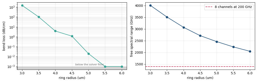
Bend loss rises steeply below 4 um and is negligible above it, so it does not constrain the design: at 5 um it is under 0.001 dB/cm, which over a 31 um round trip is far below the junction loss added later. The free spectral range falls as the radius grows, and the eight channels have to fit inside it.
The ring radius is 5 um. It sits a micron clear of the bend-loss knee, which at roughly a factor of ten per half micron is a wide margin, and its free spectral range of about 2.5 THz leaves the eight channels using well under two thirds of it.
This solve covers radiation loss only. It finds the mode of a perfectly smooth waveguide, so no other loss mechanism appears. What actually limits a passive silicon waveguide is scattering from sidewall roughness, which depends on lithography and etch rather than on the mode and has to be supplied from process data. The scattering_db_cm set at the top of the notebook carries it, and it is added to every ring.
The thermo-optic sensitivity
Every ring on this chip has a heater, so how far a resonance moves per kelvin is a number the rest of the notebook depends on. It comes from solving the same bend mode twice with the silicon and oxide indices shifted by their thermo-optic coefficients, which is a change to the technology rather than to the solve.
[6]:
# Thermo-optic coefficients at 1550 nm: silicon and silica.
dn_dt_si, dn_dt_ox = 1.86e-4, 9.5e-6
n_si = td.material_library["cSi"]["Palik_NoLoss"].nk_model(frequency=f0)[0]
n_ox = td.material_library["SiO2"]["Palik_Lossless"].nk_model(frequency=f0)[0]

n_hot_cold = []
# Calculate the bend mode effective index at two temperatures
for delta_t in (0.0, 20.0):
    # Rebuild the technology with both indices shifted by the thermo-optic effect
    hot = optical_io_soi(
        si={
            "optical": td.Medium(permittivity=(n_si + dn_dt_si * delta_t) ** 2),
            "electrical": si["electrical"],
        },
        sio2={
            "optical": td.Medium(permittivity=(n_ox + dn_dt_ox * delta_t) ** 2),
            "electrical": sio2["electrical"],
        },
    )
    # Same wide window as the bend study, so only the temperature differs
    spec = hot.ports["Rib_TE_1550_500"].copy()
    spec.width = 2 * r_target - 0.2
    spec.limits = (-2.0, 2.0)
    spec.added_solver_modes = 6
    port = pf.Port(center=(0, 0), input_direction=0, spec=spec, bend_radius=r_target)
    mode_solver = pf.port_modes(
        port, frequencies=[f0], mesh_refinement=30, technology=hot, verbose=False
    )
    info = mode_solver.data.modes_info

    # Pull the solved modes out as flat arrays
    area = np.array(info["mode area"].values).ravel()
    n_eff = np.array(info["n eff"].values).ravel()

    # Identify the guided branch by area, as in the bend study
    guided = np.where(area < 1.0)[0]
    n_hot_cold.append(float(n_eff[guided[np.argmin(area[guided])]]))

# Index shift per kelvin, from the two solves twenty degrees apart
dn_eff_dt = (n_hot_cold[1] - n_hot_cold[0]) / 20.0
# Convert that to a resonance shift per kelvin, one per waveguide type
ghz_per_k_rib = f0 * dn_eff_dt / bend[r_target]["n_group"] * 1e-9
print(f"dn_eff/dT = {dn_eff_dt:.4e} /K")
print(
    f"rib resonance shift = {ghz_per_k_rib:.2f} GHz/K "
    f"= {ghz_per_k_rib / 0.125:.1f} pm/K"
)
Progress: 100%
Progress: 100%
dn_eff/dT = 1.8672e-04 /K
rib resonance shift = 9.31 GHz/K = 74.5 pm/K
The junction
The modulator works by depleting a reverse-biased p-n junction that sits across the waveguide core. Removing free carriers raises the refractive index and lowers the absorption, so the resonance moves and the ring becomes slightly more transparent at the same time.
Both effects come from the same carriers, which is why the doping cannot be chosen from the efficiency alone, and why this section measures rather than assumes. Each recipe is run twice: a charge solve for the carrier distribution against bias, then a mode solve of the same cross-section with silicon replaced by a medium whose index and absorption follow those carriers.
The charge solve follows the workflow of the Tidy3D charge solver example, which is worth reading first for what the mesh settings and the boundary conditions mean. Two details here are specific to this device:
The waveguide runs along x. A port cross-section in PhotonForge lies in the plane normal to propagation, so putting the guide along x makes the charge plane and the optical mode plane the same plane. Drawing the junction along y instead leaves the carrier data interpolated along the wrong axis, which produces a plausible but badly wrong loss.
One drawing feeds both solves.
Component.extrude(classification="electrical")applies the same extrusion rules used for the optical stack, but picks the charge medium out of eachMultiPhysicsMedium, so the doped regions arrive asSemiconductorMediumwith their doping already attached. The optical solve needs even less: the port specification produces the mode solver straight from the same technology.The heavy implants are inside the optical window. The carrier monitor covers the whole cross-section, so the p++ and n++ regions contribute their free-carrier absorption to the mode along with the junction itself. Their setback from the core is therefore a real optical parameter, not just an electrical one.
The fine mesh is sized from the doping. A reverse-biased junction is sensitive to the mesh where the depletion edges move and almost indifferent everywhere else, so the 2 nm region spans the depletion width at the largest bias plus six Debye lengths, which is the distance over which the carriers climb back to their bulk values on either side. Both terms come from the doping, so the window follows it: 167 nm for the lightest recipe here and 52 nm for the heaviest. Fixing it instead means it is either too small for light doping or wasteful for heavy doping, and only one of those two failures shows up in the answer.
[7]:
bias = np.round(np.linspace(0, 3.0, 7), 3)  # the drive range, characterised end to end

# Cross-section geometry, measured out from the middle of the core
slab_half, x_ohmic, x_contact, guide_length = 3.0, 0.8, 1.2, 4.0

# Silicon constants at 300 K, used to size the mesh below
eps_si = 11.7 * 8.854e-14  # F/cm
q_e, v_thermal, n_intrinsic = 1.602e-19, 0.02585, 1.0e10  # C, volts, cm^-3


def junction_at(n_a, n_d):
    """Charge solve plus perturbed mode solve for one implant recipe."""
    # Build a short label for task names and cache files
    tag = f"na{n_a:.0e}_nd{n_d:.0e}".replace("+", "").replace("e0", "e")

    # Rebuild the technology with this implant pair
    t = optical_io_soi(si_p=silicon("Si p", n_a=n_a), si_n=silicon("Si n", n_d=n_d))

    # Draw the cross-section, with the guide along x and the junction along y
    cell = pf.Component(f"junction_{tag}", technology=t)
    cell.add(
        "Si Slab",
        pf.Rectangle((-guide_length / 2, -slab_half), (guide_length / 2, slab_half)),
        "Si",
        pf.Rectangle((-guide_length / 2, -w_core / 2), (guide_length / 2, w_core / 2)),
        "Si p",
        pf.Rectangle((-guide_length / 2, -slab_half), (guide_length / 2, 0)),
        "Si n",
        pf.Rectangle((-guide_length / 2, 0), (guide_length / 2, slab_half)),
        "Si p++",
        pf.Rectangle((-guide_length / 2, -slab_half), (guide_length / 2, -x_ohmic)),
        "Si n++",
        pf.Rectangle((-guide_length / 2, x_ohmic), (guide_length / 2, slab_half)),
        "Contact",
        pf.Rectangle((-guide_length / 2, -slab_half), (guide_length / 2, -x_contact)),
        pf.Rectangle((-guide_length / 2, x_contact), (guide_length / 2, slab_half)),
    )
    # Work out the built-in potential, then the depletion width at full bias
    v_built_in = v_thermal * np.log(n_a * n_d / n_intrinsic**2)
    w_depletion = 1e4 * np.sqrt(
        2 * eps_si * (v_built_in + bias[-1]) / q_e * (1 / n_a + 1 / n_d)
    )
    debye = 1e4 * np.sqrt(eps_si * v_thermal / (q_e * min(n_a, n_d)))

    # Set the finely meshed window to the depletion width plus six Debye lengths
    fine_window = w_depletion + 6 * debye
    print(
        f"{tag}: depletion {w_depletion*1e3:.0f} nm and Debye {debye*1e3:.1f} nm "
        f"at {bias[-1]:.0f} V, fine mesh over {fine_window*1e3:.0f} nm"
    )

    # Name the two contacts, since voltage conditions attach to named structures
    charge_structures = [
        (
            s.updated_copy(
                name="contact_p" if s.geometry.bounds[0][1] < 0 else "contact_n"
            )
            if s.medium.name == "W"
            else s
        )
        for s in (x.to_tidy3d() for x in cell.extrude(classification="electrical"))
    ]

    # Build the charge simulation on a plane, since nothing varies along the guide
    charge_sim = td.HeatChargeSimulation(
        center=(0, 0, 0.5),
        size=(0, 7.0, 3.0),  # charge simulation plane: zero thickness along the guide
        structures=charge_structures,
        medium=sio2["electrical"],
        monitors=[
            # Measure the capacitance per unit length
            td.SteadyCapacitanceMonitor(
                center=(0, 0, 0.11), size=(0, td.inf, td.inf), name="capacitance"
            ),
            # Measure the carriers everywhere, for the optical solve that follows
            td.SteadyFreeCarrierMonitor(
                center=(0, 0, 0.11),
                size=(0, td.inf, td.inf),
                name="carriers",
                unstructured=True,
            ),
        ],
        boundary_spec=[
            # Ground the p side and sweep the n side positive, which reverse biases it
            td.HeatChargeBoundarySpec(
                condition=td.VoltageBC(source=td.DCVoltageSource(voltage=0)),
                placement=td.StructureBoundary(structure="contact_p"),
            ),
            td.HeatChargeBoundarySpec(
                condition=td.VoltageBC(source=td.DCVoltageSource(voltage=list(bias))),
                placement=td.StructureBoundary(structure="contact_n"),
            ),
        ],
        grid_spec=td.DistanceUnstructuredGrid(
            dl_interface=0.01,  # Element size at interfaces, um
            dl_bulk=0.15,  # far from the junction nothing varies
            distance_interface=0.02,
            distance_bulk=0.6,
            relative_min_dl=0,  # Smallest element, as a fraction of the domain
            sampling=800,
            mesh_refinements=[
                # Mesh the depletion region at 2 nm
                td.GridRefinementRegion(
                    center=(0, 0, 0.11),
                    # 220 nm of core, with 20 nm of oxide above and below
                    size=(0, fine_window, 0.26),
                    dl_internal=0.002,
                    transition_thickness=0.1,
                ),
                td.GridRefinementRegion(
                    center=(0, 0, 0.11),
                    size=(0, 2.0, 0.4),
                    dl_internal=0.01,
                    transition_thickness=0.3,
                ),
            ],
        ),
        # Solve at fixed temperature with Fermi statistics, which these densities need
        analysis_spec=td.IsothermalSteadyChargeDCAnalysis(
            temperature=300, fermi_dirac=True
        ),
    )

    # Run the charge solve, which meshes from the grid above
    charge_data = web.Job(
        simulation=charge_sim,
        task_name=f"oio_charge_{tag}",
    ).run(path=f"data_charge_{tag}.hdf5")

    # Take the carrier distribution, one map per bias point
    carriers = charge_data["carriers"]

    # Refine the optical mesh across the junction, where the carriers change fastest
    junction_grid = td.MeshOverrideStructure(
        geometry=td.Box(center=(0, 0, 0.11), size=(td.inf, 0.6, 0.3)),
        dl=(0.02, 0.002, 0.005),
    )

    # Key the mode cache on everything the solve depends on
    key = hashlib.sha256(
        repr(
            (
                n_a,
                n_d,
                list(bias),
                r_target,
                lda0,
                25,  # min_steps_per_wvl
                tuple(junction_grid.dl),
                tuple(junction_grid.geometry.size),
                fine_window,
                (slab_half, x_ohmic, x_contact, guide_length),
                repr(t.ports["Rib_TE_1550_500"]),
            )
        ).encode()
    ).hexdigest()[:16]
    cached = pathlib.Path(f"modes_{tag}_{key}.npz")

    if cached.is_file():
        with np.load(cached) as stored:
            n_eff, loss_db_cm = stored["n_eff"], stored["loss_db_cm"]
    else:
        # Build one mode solver per bias point
        solvers = []
        for v in bias:
            # Hand the carrier distribution to the silicon medium
            perturbed = si_perturb.perturbed_copy(
                electron_density=carriers.electrons.sel(voltage=v),
                hole_density=carriers.holes.sel(voltage=v),
            )
            # Rebuild the technology around it, so the port spec builds the solver
            biased = optical_io_soi(
                si={"optical": perturbed, "electrical": si["electrical"]}
            )
            ms = biased.ports["Rib_TE_1550_500"].to_tidy3d(
                frequencies=[f0], technology=biased
            )
            ms = ms.updated_copy(
                # Solve in the bend, at a radius that pushes the mode onto the n side
                mode_spec=ms.mode_spec.updated_copy(bend_radius=r_target),
                simulation=ms.simulation.updated_copy(
                    grid_spec=td.GridSpec.auto(
                        wavelength=lda0,
                        min_steps_per_wvl=25,
                        override_structures=[junction_grid],
                    )
                ),
            )
            # Clip each solver to its mode plane. The perturbed medium carries a
            # carrier map over the whole cell, so this is 14 MB down to 4 MB.
            solvers.append(ms.reduced_simulation_copy)

        # A sequence solves in one batch
        modes = pf.port_modes(solvers, task_name=f"oio_modes_{tag}", verbose=False)

        # Read mode 0, the only mode this port carries
        n_eff, loss_db_cm = [], []
        for solved in modes:
            info = solved.data.modes_info
            n_eff.append(float(info["n eff"].isel(mode_index=0).item()))
            loss_db_cm.append(float(info["loss (dB/cm)"].isel(mode_index=0).item()))

        # Cache the two arrays, which is a file of a few hundred bytes
        np.savez(cached, n_eff=n_eff, loss_db_cm=loss_db_cm)

    # Average the electron and hole capacitance, per unit length
    cap = charge_data["capacitance"]

    # Collect everything this recipe produced
    result = dict(
        tag=tag,
        n_a=n_a,
        n_d=n_d,
        n_eff=np.array(n_eff),
        loss_db_cm=np.array(loss_db_cm),
        capacitance=0.5
        * (
            np.abs(np.array(cap.electron_capacitance.data))
            + np.abs(np.array(cap.hole_capacitance.data))
        ),
    )
    # Fit a quadratic, since depletion is sublinear and one slope would miss the top
    qn = np.polyfit(bias, result["n_eff"] - result["n_eff"][0], 2)
    ql = np.polyfit(bias, result["loss_db_cm"] - result["loss_db_cm"][0], 2)
    result["dn_dv"], result["dn_dv2"] = qn[1], qn[0]
    result["dloss_dv"], result["dloss_dv2"] = ql[1], ql[0]
    return result


# Take the silicon index without loss, so every dB comes from free carriers
n_si = td.material_library["cSi"]["Palik_NoLoss"].nk_model(frequency=f0)[0]

# Attach the Nedeljkovic-Soref-Mashanovich fits for index and absorption change
nsm = td.NedeljkovicSorefMashanovich(ref_freq=f0)
si_perturb = td.PerturbationMedium.from_unperturbed(
    medium=td.medium_from_nk(n=n_si, k=0, freq=f0),
    perturbation_spec=td.IndexPerturbation(
        delta_n=nsm.delta_n(), delta_k=nsm.delta_k(), freq=f0
    ),
)

# Characterise three implant recipes, an order of magnitude apart end to end
junctions = [
    junction_at(*doping) for doping in ((7e17, 5e17), (3e18, 2e18), (8e18, 5e18))
]
na7e17_nd5e17: depletion 132 nm and Debye 5.8 nm at 3 V, fine mesh over 167 nm
06:19:15 -03 Created task 'oio_charge_na7e17_nd5e17_mesh' with resource_id
             'vom-39c38f3e-c070-4048-b4f7-b702ebe5d681' and task_type
             'VOLUME_MESH'.
             Tidy3D's VolumeMesher solver is currently in the beta stage. Cost
             of VolumeMesher simulations is subject to change in the future.
06:19:18 -03 Estimated FlexCredit cost: 0.025. Use 'web.real_cost(task_id)' to
             get the billed FlexCredit cost after a simulation run.
06:19:20 -03 status = queued
             To cancel the simulation, use 'web.abort(task_id)' or
             'web.delete(task_id)' or abort/delete the task in the web UI.
             Terminating the Python script will not stop the job running on the
             cloud.
06:19:29 -03 starting up solver
running solver
06:19:39 -03 status = success
06:19:40 -03 Loading simulation from local cache. View cached task using web UI
             at
             'https://tidy3d.simulation.cloud/workbench?taskId=hec-195c2bb4-4763
             -46d4-af66-2325b0a68c96'.
na3e18_nd2e18: depletion 66 nm and Debye 2.9 nm at 3 V, fine mesh over 83 nm
             Created task 'oio_charge_na3e18_nd2e18_mesh' with resource_id
             'vom-efcc940f-6f52-45c4-8252-28c2ad9198d3' and task_type
             'VOLUME_MESH'.
             Tidy3D's VolumeMesher solver is currently in the beta stage. Cost
             of VolumeMesher simulations is subject to change in the future.
06:19:43 -03 Estimated FlexCredit cost: 0.025. Use 'web.real_cost(task_id)' to
             get the billed FlexCredit cost after a simulation run.
06:19:45 -03 status = queued
             To cancel the simulation, use 'web.abort(task_id)' or
             'web.delete(task_id)' or abort/delete the task in the web UI.
             Terminating the Python script will not stop the job running on the
             cloud.
06:19:54 -03 starting up solver
06:19:55 -03 running solver
06:20:04 -03 status = success
06:20:05 -03 Loading simulation from local cache. View cached task using web UI
             at
             'https://tidy3d.simulation.cloud/workbench?taskId=hec-b4632d6c-8bc7
             -4a2d-ae12-b484fd88458b'.
na8e18_nd5e18: depletion 41 nm and Debye 1.8 nm at 3 V, fine mesh over 52 nm
             Created task 'oio_charge_na8e18_nd5e18_mesh' with resource_id
             'vom-421f6fe5-3545-4e30-99cf-a36718f95d5c' and task_type
             'VOLUME_MESH'.
             Tidy3D's VolumeMesher solver is currently in the beta stage. Cost
             of VolumeMesher simulations is subject to change in the future.
06:20:08 -03 Estimated FlexCredit cost: 0.025. Use 'web.real_cost(task_id)' to
             get the billed FlexCredit cost after a simulation run.
06:20:10 -03 status = queued
             To cancel the simulation, use 'web.abort(task_id)' or
             'web.delete(task_id)' or abort/delete the task in the web UI.
             Terminating the Python script will not stop the job running on the
             cloud.
06:20:19 -03 starting up solver
06:20:20 -03 running solver
06:20:29 -03 status = success
06:20:30 -03 Loading simulation from local cache. View cached task using web UI
             at
             'https://tidy3d.simulation.cloud/workbench?taskId=hec-724d899a-3b17
             -4aa2-abda-334f5a3e4516'.
[8]:
# Compare the three doping recipes on the four numbers that decide the design
print(
    f"{'N_a':>9s} {'N_d':>9s} {'loss dB/cm':>11s} {'dn/dV':>11s} {'VpiL V.cm':>10s} {'C fF/um':>8s}"
)
for j in junctions:
    # Average the index slope over the drive range, which is what VpiL means
    slope = (j["n_eff"][-1] - j["n_eff"][0]) / (bias[-1] - bias[0])
    print(
        f"{j['n_a']:9.1e} {j['n_d']:9.1e} {j['loss_db_cm'][0]:11.1f} {slope:11.3e} "
        f"{lda0 * 1e-4 / (2 * slope):10.3f} {j['capacitance'][0]:8.3f}"
    )
      N_a       N_d  loss dB/cm       dn/dV  VpiL V.cm  C fF/um
  7.0e+17   5.0e+17        31.3   4.825e-05      1.606    0.405
  3.0e+18   2.0e+18        94.7   8.309e-05      0.933    0.737
  8.0e+18   5.0e+18       251.6   1.180e-04      0.657    1.108
[9]:
# Plot index, loss and capacitance against bias, one curve per recipe
fig, ax = plt.subplots(1, 3, figsize=(14, 3.6))
for j, color in zip(junctions, ("#1f4e79", "#3aa596", "#c8385a")):
    label = f"{j['n_a']:.0e} / {j['n_d']:.0e}"

    # Index shift, the quantity that tunes the resonance
    ax[0].plot(bias, (j["n_eff"] - j["n_eff"][0]) * 1e4, "o-", color=color, label=label)

    # Absorption, which the doping buys the index shift with
    ax[1].plot(bias, j["loss_db_cm"], "o-", color=color, label=label)

    # Plot the capacitance, which sets the electrical bandwidth
    ax[2].plot(bias, j["capacitance"], "o-", color=color, label=label)
ax[0].set_ylabel("index change (1e-4)")
ax[1].set_ylabel("loss (dB/cm)")
ax[2].set_ylabel("capacitance (fF/um)")
for a in ax:
    a.set_xlabel("reverse bias (V)")
    a.grid(alpha=0.3)
    a.legend(fontsize=8)
plt.tight_layout()
plt.show()
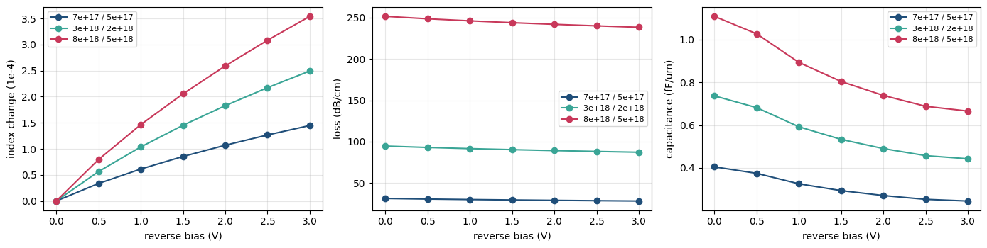
The capacitance falls with reverse bias, as it must for a widening depletion region, and the loss falls with it because the same carriers that carried the charge were absorbing the light.
Raising the doping by a factor of ten multiplies the index change by about two and a half and the loss by more than an order of magnitude: efficiency grows roughly as the square root of the doping while absorption grows almost linearly. The usual conclusion is that the lightest doping with acceptable efficiency wins, because it has the best ratio of the two. The next section shows why that is wrong for a ring.
The bus coupler
Before the doping can be chosen, the coupling has to be something that can be dialled in, which means knowing the gap that produces a given coupling. Coupling into a ring is not a directional-coupler formula here: the two waveguides are close only over a short arc and their separation changes continuously along it, so it is measured with FDTD.
Only the bus input is excited, which is one simulation per gap rather than four, and the coupled power is read at the far end of the half ring.
This coupler is very nearly lossless, so the scattered powers have to add up to one, and that sum is the check worth printing. It catches two mistakes that are easy to make and quiet when made.
With a short bus the input and through port planes sit close enough to the ring that their mode profiles overlap it, each port reads some of the other waveguide, and the total comes out near 1.07. Extending the bus fixes it and moves the coupling by 8 percent.
The second one is worth more care, because the healthy-looking column hides it. The sum has to be checked from every input port, not just the bus. The ring-side ports sit on the ends of a 5 um arc, where the guided field is the bend mode rather than the straight one, and a port left on the straight mode throws away the difference. Driven from the bus the balance reads 0.995 and looks fine; driven from the arc it reads 0.917. Setting port_bends recovers most of that.
[10]:
# Gaps to sweep, spanning the range a ring coupler is usually built in
gaps = np.array([0.12, 0.16, 0.20, 0.26])
kappa_squared = []

# Build and simulate one coupler per gap
for gap_value in gaps:
    coupler = pf.parametric.ring_coupler(
        port_spec="Rib_TE_1550_500",
        radius=r_target,
        coupling_distance=w_core + gap_value,
        bus_length=5.0,  # far enough that the ports miss the ring field
        coupling_length=0,
        euler_fraction=0.0,
        port_bends=True,  # arc-end ports need the bend mode, not the straight one
        # Mesh at grid 14, where refining to 18 moves the coupling by 1.4 percent
        model=pf.Tidy3DModel(
            grid_spec=14,
            verbose=False,
            # Reuse the mirror symmetry, so P0 stands in for P2 and P1 for P3
            port_symmetries=[("P2", "P3", "P0", "P1")],
        ),
    )
    # Drive the bus alone, which is one run per gap instead of four
    s = coupler.s_matrix([f0], model_kwargs={"inputs": ["P0"]})

    # Take the power that crosses into the ring and the power left on the bus
    kappa_squared.append(float(np.abs(s[("P0@0", "P3@0")][0]) ** 2))
    through = float(np.abs(s[("P0@0", "P2@0")][0]) ** 2)
    print(
        f"gap {gap_value*1e3:4.0f} nm   kappa^2 = {kappa_squared[-1]:.4f}   "
        f"through = {through:.4f}   sum = {kappa_squared[-1] + through:.4f}"
    )

kappa_squared = np.array(kappa_squared)

# Fit log coupling against gap, which is a line because the tail decays exponentially
gap_fit = np.polyfit(gaps, np.log10(kappa_squared), 1)

# Invert the fit, to get the gap that produces a wanted coupling
gap_for = lambda k2: (np.log10(k2) - gap_fit[1]) / gap_fit[0]
Progress: 100%
gap  120 nm   kappa^2 = 0.1523   through = 0.8447   sum = 0.9970
Progress: 100%
gap  160 nm   kappa^2 = 0.0956   through = 0.9025   sum = 0.9980
Progress: 100%
gap  200 nm   kappa^2 = 0.0599   through = 0.9387   sum = 0.9986
Progress: 100%
gap  260 nm   kappa^2 = 0.0295   through = 0.9697   sum = 0.9993
One caveat on how that was measured, because it decides what the rest of the notebook may use it for. The bus was the excited port, and the sums above say that excitation conserves power to about a part in a thousand. Driving the ring arc instead loses roughly ten times as much, and almost none of it is real: a mode solve puts the loss of this bend at zero. Terminating a curved waveguide on a port costs about a hundredth of a dB in FDTD whatever the mesh, and a resonator multiplies that by its finesse.
The coupling therefore comes from this sweep, while the ring loss comes from the mode solver and the process figure.
Choosing the doping and the coupling
A ring is deepest when its coupling matches its round-trip loss, which is critical coupling. Couple harder and the resonance widens but goes shallow. Since a ring cannot respond faster than its own photon lifetime, and that lifetime is set by the linewidth, width is what the line rate needs and depth is what the extinction needs.
The point that decides this design is that there are two ways to widen a resonance and they are not equivalent. Coupling harder widens it by letting light escape, which moves the ring away from critical coupling and makes it shallow. Adding loss widens it too, but the critical coupling moves with the loss, so a lossier ring can be wide and still sit at its own critical point. Loss also comes with better efficiency here, because the same doping that absorbs also modulates. So bandwidth should be bought with doping before it is bought with coupling.
The scan below is over both. For each doping and each multiple of that recipe’s own critical coupling it reports:
kappa^2, the power coupling, and the gap that produces it from the fit above,
FWHM, the resonance width, and cavity, the photon-lifetime bandwidth it allows, which is half the linewidth,
cold ER, the depth of the unmodulated resonance, which is infinite exactly at critical,
ER at 4 dB, the extinction between the two drive levels at the laser detuning where the bright level costs 4 dB of insertion loss. That last one is the number the link sees.
Two assumptions are fixed throughout and both matter: the junction is driven with 3 V from a 50 ohm source, and only the part of the ring that carries the junction contributes modulation.
[11]:
doped_sector_degrees = 260  # Angular extent of the junction, degrees of 360
doped_fraction = doped_sector_degrees / 360

v_drive = 3.0  # drive swing, and the range the junction was characterised over
z0_driver = 50.0  # source impedance the junction is driven from
il_operating = 4.0  # insertion loss the link can afford on the bright level


def ring_at(junction, kappa2, radius=None):
    """Ring model for one junction recipe and coupling, with ring-averaged terms."""
    # Default to the chosen radius, and take that ring's measured bend data
    radius = r_target if radius is None else radius
    length = 2 * np.pi * radius
    b = bend[radius]
    # Add up the round-trip loss: bend radiation, sidewall scattering, junction
    loss_db_um = (
        b["loss"] + scattering_db_cm + doped_fraction * junction["loss_db_cm"][0]
    ) * 1e-4
    # Round the index to put a resonance exactly on the carrier
    n_eff = round(b["n_eff"] * length / lda0) * lda0 / length
    # Scale every junction slope by the fraction of the ring it covers
    return pf.RingModel(
        kappa1=1j * np.sqrt(kappa2),
        n_eff=n_eff,
        n_group=b["n_group"],
        length=length,
        propagation_loss=loss_db_um,
        reference_frequency=f0,
        dn_dv=doped_fraction * junction["dn_dv"],
        dn_dv2=doped_fraction * junction["dn_dv2"],
        dloss_dv=doped_fraction * junction["dloss_dv"] * 1e-4,
        dloss_dv2=doped_fraction * junction["dloss_dv2"] * 1e-4,
        ports=["P0", "P1"],
    )


def extinction(model, cell, fsr, drive=v_drive, il_target=il_operating):
    """Extinction at the detuning where the bright level costs il_target."""
    # Scan either side of the carrier, finely enough to resolve the resonance
    freqs = f0 + np.linspace(-0.3, 0.3, 6001) * fsr

    # Measure the unbiased transmission, which is the dark level
    model.update(voltage=0.0)
    dark = np.abs(cell.s_matrix(freqs)[("P0@0", "P1@0")]) ** 2
    # Measure the driven transmission, which is the bright level
    model.update(voltage=drive)
    bright = np.abs(cell.s_matrix(freqs)[("P0@0", "P1@0")]) ** 2

    # Put the model back where it was found, so callers are not surprised
    model.update(voltage=0.0)

    # Work out the extinction between the levels and the loss of the bright one
    er = 10 * np.log10(np.maximum(bright, 1e-12) / np.maximum(dark, 1e-12))
    il = -10 * np.log10(np.maximum(bright, 1e-12))
    # Measure each point's distance from the insertion loss the link can afford
    d = il - il_target
    best = (np.nan, np.nan)

    # Walk every sign change and interpolate to the crossing, keeping the best
    for i in np.where(np.sign(d[:-1]) != np.sign(d[1:]))[0]:
        w = d[i] / (d[i] - d[i + 1])
        e = er[i] + w * (er[i + 1] - er[i])
        if np.isnan(best[0]) or e > best[0]:
            best = (e, freqs[i] + w * (freqs[i + 1] - freqs[i]) - f0)
    return best
[12]:
# Take the bend data and round-trip length for the chosen radius
b = bend[r_target]
length = 2 * np.pi * r_target

print(
    f"{'N_a':>8s} {'k2/crit':>8s} {'kappa^2':>8s} {'gap nm':>7s} {'FWHM':>7s} "
    f"{'cavity':>7s} {'cold ER':>8s} {'ER 4dB':>7s}"
)
# Compare every doping against several multiples of its own critical coupling
for j in junctions:

    # Add up the ring's distributed loss for this recipe
    ring_loss = b["loss"] + scattering_db_cm + doped_fraction * j["loss_db_cm"][0]
    # Convert it to round-trip power and amplitude transmission
    a2 = 10 ** (-ring_loss * 1e-4 * length / 10)
    a = np.sqrt(a2)

    # Set critical coupling, where the coupler matches the round-trip amplitude
    j["critical"] = 1 - a2

    # Step through multiples of that critical point
    for ratio in (0.8, 1.0, 1.2, 1.5, 2.0):
        kappa2 = ratio * j["critical"]
        t = np.sqrt(1 - kappa2)

        # Work out the linewidth and the unmodulated depth
        fwhm = b["fsr"] * (1 - t * a) / (np.pi * np.sqrt(t * a))
        cold = -10 * np.log10(max(((t - a) / (1 - t * a)) ** 2, 1e-12))

        # Wrap the model in a bare two-port cell so it can be swept
        model = ring_at(j, kappa2)
        cell = model.black_box_component(port_spec="Rib_TE_1550_500")

        # Measure the extinction this recipe reaches at that insertion loss
        er, _ = extinction(model, cell, b["fsr"])
        print(
            f"{j['n_a']:8.0e} {ratio:8.1f} {kappa2:8.4f} {gap_for(kappa2)*1e3:7.0f} "
            f"{fwhm*1e-9:7.1f} {fwhm/2e9:7.1f} {cold:8.1f} {er:7.2f}"
        )
     N_a  k2/crit  kappa^2  gap nm    FWHM  cavity  cold ER  ER 4dB
Progress: 100%
Progress: 100%
   7e+17      0.8   0.0141     323    12.5     6.3     19.0   14.17
Progress: 100%
Progress: 100%
   7e+17      1.0   0.0177     304    13.9     7.0    120.0   24.65
Progress: 100%
Progress: 100%
   7e+17      1.2   0.0212     289    15.4     7.7     20.7   13.76
Progress: 100%
Progress: 100%
   7e+17      1.5   0.0265     269    17.5     8.7     13.9    8.38
Progress: 100%
Progress: 100%
   7e+17      2.0   0.0353     245    21.0    10.5      9.4    4.81
Progress: 100%
Progress: 100%
   3e+18      0.8   0.0397     235    35.8    17.9     18.9    6.76
Progress: 100%
Progress: 100%
   3e+18      1.0   0.0497     216    39.9    19.9    120.0    5.93
Progress: 100%
Progress: 100%
   3e+18      1.2   0.0596     200    44.0    22.0     20.6    5.02
Progress: 100%
Progress: 100%
   3e+18      1.5   0.0745     181    50.3    25.1     13.7    3.94
Progress: 100%
Progress: 100%
   3e+18      2.0   0.0993     157    60.9    30.5      9.2    2.74
Progress: 100%
Progress: 100%
   8e+18      0.8   0.0995     156    93.2    46.6     18.6    2.61
Progress: 100%
Progress: 100%
   8e+18      1.0   0.1244     137   104.2    52.1    120.0    2.34
Progress: 100%
Progress: 100%
   8e+18      1.2   0.1493     122   115.5    57.7     20.2    2.08
Progress: 100%
Progress: 100%
   8e+18      1.5   0.1867     103   133.1    66.6     13.3    1.74
Progress: 100%
Progress: 100%
   8e+18      2.0   0.2489      78   164.4    82.2      8.7    1.31
The lightest recipe cannot be made fast at all: even at twice critical its resonance is only about ten gigahertz wide, because there is almost nothing in the ring to broaden it. Its excellent efficiency-to-loss ratio buys nothing, since the ring has no bandwidth to spend it on.
Compare the two ways of reaching a given bandwidth. The middle recipe at twice critical gets to about 25 GHz of cavity bandwidth and gives up most of its depth to do it. The heavy recipe reaches roughly twice that bandwidth while sitting at its own critical point, where the resonance is deepest, and it does so with the better efficiency of the three. Bought with coupling, bandwidth costs depth; bought with doping, it comes with depth and efficiency attached.
The modulator uses the heavy junction, coupled slightly above critical. Its linewidth lands near a hundred gigahertz, which is where published ring modulators at this line rate actually sit, and it keeps a usable extinction ratio at an affordable insertion loss.
Critical coupling looks best in the table but is not a usable operating point. Transmission at resonance goes to zero there, so the unmodulated extinction is unbounded: the reported figure is a singularity rather than a margin, and no fabricated ring lands on it. Over-coupling slightly also puts the device on the forgiving side of that point, because loss that drifts upward raises the critical coupling toward a fixed kappa and deepens the resonance, where under-coupling would wash it out.
[13]:
junction = junctions[2]  # the heavy recipe

coupling_ratio = 1.2  # Bus coupling, as a multiple of critical coupling
kappa2 = coupling_ratio * junction["critical"]
gap = gap_for(kappa2)

# Work out the arc length the junction covers
junction_length = doped_fraction * length

# Scale the measured capacitance per micron up to that arc, at mid bias
c_junction = junction["capacitance"][len(bias) // 2] * junction_length

q_e = 1.602e-19  # Electron charge, C
core_t, slab_t = 0.22e-4, 0.09e-4  # Core and slab thickness, cm

# Current path length in the core and in the slab, cm
core_path, slab_path = (w_core / 2) * 1e-4, (x_ohmic - w_core / 2) * 1e-4


def access_ohms(n, mu):
    """Sheet resistance times squares, through the core and then the slab."""
    # Cross the full-thickness core, then the thinner and more resistive slab
    r_core = 1 / (q_e * n * mu * core_t) * core_path
    r_slab = 1 / (q_e * n * mu * slab_t) * slab_path

    # Divide by the arc the junction covers, since both are per unit length
    return (r_core + r_slab) / (junction_length * 1e-4)


def caughey_thomas(m, n):
    """Low-field mobility at doping n, from the technology's own parameters."""
    return m.mu_min + (m.mu - m.mu_min) / (1 + (n / m.ref_N) ** m.exp_N)


# Take each side's majority-carrier mobility at its own doping
mu_p = caughey_thomas(si_charge.mobility_p, junction["n_a"])
mu_n = caughey_thomas(si_charge.mobility_n, junction["n_d"])

# Add the two sides' access resistance in series
r_p, r_n = access_ohms(junction["n_a"], mu_p), access_ohms(junction["n_d"], mu_n)
r_series = r_p + r_n

# Work out the RC pole, with the driver's impedance in series with the access
f_rc = 1 / (2 * np.pi * (r_series + z0_driver) * c_junction * 1e-15)

print(
    f"ring loss        {b['loss'] + scattering_db_cm + doped_fraction * junction['loss_db_cm'][0]:.1f} dB/cm"
)
print(
    f"critical kappa^2 = {junction['critical']:.4f}, chosen {kappa2:.4f} "
    f"({coupling_ratio:.1f}x critical), coupler gap {gap*1e3:.0f} nm"
)
print(
    f"mobility         holes {mu_p:.0f}, electrons {mu_n:.0f} cm^2/(V s) "
    f"at {junction['n_a']:.0e} / {junction['n_d']:.0e}"
)
print(
    f"junction         {c_junction:.1f} fF, access {r_series:.0f} ohm "
    f"({r_p:.0f} p + {r_n:.0f} n), driver {z0_driver:.0f} ohm"
)
print(
    f"  loaded RC pole {f_rc*1e-9:.0f} GHz "
    f"(the driver matters: without it this would read "
    f"{1/(2*np.pi*r_series*c_junction*1e-15)*1e-9:.0f})"
)
ring loss        183.7 dB/cm
critical kappa^2 = 0.1244, chosen 0.1493 (1.2x critical), coupler gap 122 nm
mobility         holes 75, electrons 143 cm^2/(V s) at 8e+18 / 5e+18
junction         18.2 fF, access 61 ohm (33 p + 28 n), driver 50 ohm
  loaded RC pole 79 GHz (the driver matters: without it this would read 143)
The modulator
The measurements are done, so the modulator can be built as one parametric cell that carries its own model. A few layout points are constraints rather than drawing choices:
The implants and the outer contact stop short of the coupling region. Doped silicon there would absorb without modulating, and a metal plug there would sit close enough to the bus to matter. The inner contact is free of that, since the whole ring interior is far from the bus, so it is drawn as a solid disc: the lowest access resistance the p side can be given.
The heater is one continuous conductor, not an arc with stubs added to it. It is drawn as a closed ring plus a tapered feed with a narrow slot cut through both, following the Microring Modulator example. Building it from separate shapes leaves notches where they meet, which is both a current crowding problem and a likely design-rule failure.
The heater feed leaves downward, on the same side as the bus, which leaves the whole top of the ring to the junction metal. The two nets then run in opposite directions and neither trace has to cross the other, which a single metal layer cannot do.
The anode is inside the ring, and nothing can reach it there. Any trace to it would have to cross the cathode or the heater. The cell solves that itself, routing the anode out to a second terminal clear of the device, so the chip sees four terminals it can reach and never has to know how they were brought out.
The slab is continuous all the way round, including under the coupler, so the rib mode never meets a discontinuity. It reaches well past the ring, for two reasons that have nothing to do with the mode: it has to extend beyond the outer contact plug, or the metal hangs over its edge onto oxide, and it is drawn as a single rectangle rather than a disc plus a strip, because a circle crossing a straight edge makes a corner too sharp for a spacing rule to accept. Neither costs anything optically. The rib mode moves by six parts in a million between a 6 um slab and a 22 um one, which is 0.3 GHz of resonance against the 10 GHz the channel plan already spends on grid snapping.
The model is attached inside the parametric function. A component built by a parametric function is re-evaluated whenever a parameter changes, so a model attached afterwards from outside would be silently dropped on the next update.
[14]:
@pf.parametric_component(name_prefix="MRM")
def microring_modulator(
    *,
    ring_radius=5.0,
    core_width=0.5,
    coupling_gap=0.19,
    slab_extent=3.2,  # how far the slab reaches past the ring, clear of the plug
    ohmic_setback=0.8,  # where the heavy implants start
    contact_inner=1.5,  # the inner plug stops this far inside the ring
    contact_outer=(1.5, 3.0),  # inward and outward edges of the outer plug
    doped_sector=(-40, 220),  # the n side stops short of the coupler
    heater_width=1.2,
    heater_slot=0.6,  # the cut that turns a closed ring into a conductor
    heater_reach=10.0,  # how far past the ring the feed extends
    bus_length=16.0,
    # Model parameters, every one measured in the sections above
    kappa1=0.34,
    n_eff=2.5769,
    n_group=3.880,
    propagation_loss=1.4e-2,
    temperature=293.0,  # Ring temperature; the heater raises it above reference
    dn_dv=0.0,
    dn_dv2=0.0,
    dloss_dv=0.0,
    dloss_dv2=0.0,
    f_3dB=0.0,
    dn_dT=0.0,
):
    # Leave the name empty, so the eight modulators become eight distinct cells
    c = pf.Component()
    r = ring_radius

    # Set where the slab stops, far enough out to clear the outer plug
    slab_outer = r + slab_extent

    # Bus centre sits one gap and one core width below the ring core
    y_bus = -(r + core_width + coupling_gap)

    # Radius of the inner plug, and the two radial edges of the outer one
    plug_inner = r - contact_inner
    outer = (r + contact_outer[0], r + contact_outer[1])

    # Angular limits of the doped sector
    a0, a1 = doped_sector

    # Draw one slab rectangle over the ring and the bus together
    slab_half = max(bus_length / 2, slab_outer)
    c.add(
        "Si Slab",
        pf.Rectangle((-slab_half, y_bus - w_slab_port / 2), (slab_half, slab_outer)),
    )

    # Add the full-thickness core on top of it
    c.add("Si", pf.Circle(r + core_width / 2, inner_radius=r - core_width / 2))

    # Add the implants, all of them confined to the doped sector
    c.add(
        "Si p",
        pf.Circle(r, sector=doped_sector),
        "Si n",
        pf.Circle(slab_outer, inner_radius=r, sector=doped_sector),
        "Si p++",
        pf.Circle(r - ohmic_setback, sector=doped_sector),
        "Si n++",
        pf.Circle(slab_outer, inner_radius=r + ohmic_setback, sector=doped_sector),
        # Add the two plugs, each ten degrees inside the doped sector
        "Contact",
        pf.Circle(plug_inner, sector=(a0 + 10, a1 - 10)),
        pf.Circle(outer[1], inner_radius=outer[0], sector=(a0 + 10, a1 - 10)),
    )

    # Closed heater loop following the ring
    heater_ring = pf.Circle(r + heater_width / 2, inner_radius=r - heater_width / 2)

    # Lower end of the heater feed, on the bus side, leaving the top for metal
    feed_bot = -(r + heater_reach)

    # Set the gap between the two heater terminals, which straddle the slot
    terminal_gap = 3.0
    terminal_x = (metal_width + terminal_gap) / 2

    # Widen the feed to hold both terminals, their vias and half a heater width
    feed_wide = 2 * (terminal_x + metal_width / 2) + heater_width / 2

    # Draw the feed straight at both ends, tapering only in between
    feed = (
        pf.Path((0, feed_bot), feed_wide)
        .segment((0, feed_bot + heater_width), feed_wide)
        .segment((0, -(r + heater_width)), 2.5 * heater_width)
        .segment((0, -r), 2.5 * heater_width)
    )

    # Cut a slot through both, turning the closed loop into a single conductor
    slot = pf.Path((0, feed_bot - 0.5), heater_slot).segment((0, 0))
    c.add("Heater", *pf.boolean([heater_ring, feed], [slot], "-"))

    # Add the bus core, whose slab came with the rectangle above
    c.add(
        "Si",
        pf.Rectangle(
            (-bus_length / 2, y_bus - core_width / 2),
            (bus_length / 2, y_bus + core_width / 2),
        ),
    )

    # Take the rib port spec, since the junction needs a slab to its contacts
    port_spec = pf.config.default_technology.ports["Rib_TE_1550_500"]

    # Optical ports at the two ends of the bus
    c.add_port(pf.Port((-bus_length / 2, y_bus), 0, port_spec), "P0")
    c.add_port(pf.Port((bus_length / 2, y_bus), 180, port_spec), "P1")

    # Add the drive as an electrical port, which is what a time stepper reads
    c.add_port(pf.Port((0, 0), 0, virtual_port_spec(classification="electrical")), "E0")

    # Add one terminal per plug, anode on the inner disc and cathode on the arc
    for name, radius in (("ANODE", 0), ("CATHODE", 0.5 * sum(outer))):
        c.add_terminal(
            pf.Terminal(
                "M1", pf.Rectangle(center=(0, radius), size=(metal_width, metal_width))
            ),
            name,
            add_structure=True,
        )

    # Carry the anode out to a second terminal, clear of the ring
    c.add_terminal(
        pf.Terminal(
            "M1",
            pf.Rectangle(center=(-(r + 8), -(r + 5)), size=(metal_width, metal_width)),
        ),
        "ANODE_ACCESS",
        add_structure=True,
    )
    # Draw the metal that carries it, since the trace is part of the device
    c.add(
        pf.parametric.route_manhattan(
            terminal1=c["ANODE"],
            terminal2=c["ANODE_ACCESS"],
            width=metal_width,
            direction2="x",
        )
    )
    # Add a heater terminal either side of the slot, each with its own via
    for name, sign in (("H0", -1), ("H1", 1)):
        c.add(
            "Via",
            pf.Rectangle(
                center=(
                    sign * terminal_x,
                    feed_bot + 0.6,
                ),
                size=(metal_width, metal_width),
            ),
        )
        c.add_terminal(
            pf.Terminal(
                "M1",
                pf.Rectangle(
                    center=(
                        sign * terminal_x,
                        feed_bot + 0.6,
                    ),
                    size=(metal_width, metal_width),
                ),
            ),
            name,
            add_structure=True,
        )

    # Round-trip length of the ring
    length = 2 * np.pi * r

    # Arguments shared by the frequency-domain model and the time stepper
    model_kwargs = dict(
        kappa1=1j * kappa1,
        n_eff=n_eff,
        n_group=n_group,
        length=length,
        propagation_loss=propagation_loss,
        reference_frequency=f0,
        dn_dv=dn_dv,
        dn_dv2=dn_dv2,
        dloss_dv=dloss_dv,
        dloss_dv2=dloss_dv2,
        dn_dT=dn_dT,
        temperature=temperature,
        ports=["P0", "P1"],
    )
    # Frequency-domain model of the ring
    model = pf.RingModel(**model_kwargs)

    # Same ring as a time stepper, so the cell can be driven with a waveform
    model.time_stepper = pf.RingTimeStepper(
        z0=50.0, f_3dB=f_3dB, verbose=False, **model_kwargs
    )

    # Attach the model inside the function, so a parameter change keeps it
    c.add_model(model, "ring")
    return c


# Build the modulator from every number measured above
mrm = microring_modulator(
    ring_radius=r_target,
    coupling_gap=round(gap, 3),
    kappa1=np.sqrt(kappa2),
    n_eff=round(b["n_eff"] * length / lda0) * lda0 / length,
    n_group=b["n_group"],
    propagation_loss=(
        b["loss"] + scattering_db_cm + doped_fraction * junction["loss_db_cm"][0]
    )
    * 1e-4,
    dn_dv=doped_fraction * junction["dn_dv"],
    dn_dv2=doped_fraction * junction["dn_dv2"],
    dloss_dv=doped_fraction * junction["dloss_dv"] * 1e-4,
    dloss_dv2=doped_fraction * junction["dloss_dv2"] * 1e-4,
    dn_dT=dn_eff_dt,
    f_3dB=f_rc,
)
viewer(mrm)
[14]:
;fill:%23221f20;font-weight:bold;font-size:1.084600px;}.terminal{fill:none;stroke:%23805080;stroke-width:0.135575;}.dashed{stroke-dasharray:0.677875,0.406725;}.port{fill:none;stroke:%23805080;stroke-width:0.271150;}.virtual-connection{fill:none;stroke:%23907090;stroke-width:0.203363;}.layer_10_0{stroke:%23878787;fill:%23888888;fill-opacity:0.094;}.label_10_0{fill:%23878787;}.layer_98_0{stroke:%23c8385a;fill:none;}.label_98_0{fill:%23c8385a;}.layer_99_0{stroke:%232e7d5b;fill:none;}.label_99_0{fill:%232e7d5b;}.layer_7_0{stroke:%237a5c99;fill:url(%23pat-layer_7_0);fill-opacity:0.492;}.label_7_0{fill:%237a5c99;}.layer_11_0{stroke:%23666666;fill:%23666666;fill-opacity:0.094;}.label_11_0{fill:%23666666;}.layer_12_0{stroke:%23b88b14;fill:url(%23pat-layer_12_0);fill-opacity:0.492;}.label_12_0{fill:%23b88b14;}.layer_14_0{stroke:%23838383;fill:%23b0b0b0;fill-opacity:0.094;}.label_14_0{fill:%23838383;}.layer_15_0{stroke:%23000000;fill:url(%23pat-layer_15_0);fill-opacity:0.492;}.label_15_0{fill:%23000000;}.layer_1_0{stroke:%231f4e79;fill:url(%23pat-layer_1_0);fill-opacity:0.492;}.label_1_0{fill:%231f4e79;}.layer_2_0{stroke:%234f8fc0;fill:url(%23pat-layer_2_0);fill-opacity:0.492;}.label_2_0{fill:%234f8fc0;}.layer_4_0{stroke:%233aa596;fill:url(%23pat-layer_4_0);fill-opacity:0.492;}.label_4_0{fill:%233aa596;}.layer_6_0{stroke:%231c6b61;fill:url(%23pat-layer_6_0);fill-opacity:0.492;}.label_6_0{fill:%231c6b61;}.layer_3_0{stroke:%23c8385a;fill:url(%23pat-layer_3_0);fill-opacity:0.492;}.label_3_0{fill:%23c8385a;}.layer_5_0{stroke:%238b1c38;fill:url(%23pat-layer_5_0);fill-opacity:0.492;}.label_5_0{fill:%238b1c38;}.layer_13_0{stroke:%23878787;fill:%23aaaaaa;fill-opacity:0.094;}.label_13_0{fill:%23878787;}</style><defs><path id=%22port-symbol%22 class=%22port%22 d=%22M 0,-0.542300 L 0.813450,0 0,0.542300%22 /><path id=%22ref-port-symbol%22 class=%22port%22 style=%22stroke-opacity:0.33;%22 d=%22M 0,-0.406725 C 0.542300,-0.406725 0.542300,0.406725 0,0.406725%22 /><circle id=%22port-bend-symbol%22 style=%22stroke-width:0;stroke:none;fill:%23805080;fill-opacity:1;%22 cx=%220%22 cy=%220%22 r=%220.244035%22 /><circle id=%22connection-symbol%22 style=%22stroke-width:0;stroke:none;fill:%23907090;fill-opacity:1;%22 cx=%220%22 cy=%220%22 r=%220.284708%22 /><pattern id=%22pat-layer_7_0%22 patternUnits=%22userSpaceOnUse%22 width=%220.677875%22 height=%220.677875%22 patternTransform=%22translate(0.598125,0.035678)%22><line x1=%220.338938%22 y1=%220%22 x2=%220.338938%22 y2=%220.677875%22 style=%22stroke:%237a5c99;stroke-width:0.067788%22 /><line x1=%220%22 y1=%220.338938%22 x2=%220.677875%22 y2=%220.338938%22 style=%22stroke:%237a5c99;stroke-width:0.067788%22 /></pattern><pattern id=%22pat-layer_12_0%22 patternUnits=%22userSpaceOnUse%22 width=%220.677875%22 height=%220.677875%22 patternTransform=%22translate(0.638000,0.642197)%22><line x1=%220%22 y1=%220.338938%22 x2=%220.677875%22 y2=%220.338938%22 style=%22stroke:%23b88b14;stroke-width:0.067788%22 /></pattern><pattern id=%22pat-layer_15_0%22 patternUnits=%22userSpaceOnUse%22 width=%220.406725%22 height=%220.406725%22 patternTransform=%22translate(0.071775,0.278286)%22><circle cx=%220.203363%22 cy=%220.203363%22 r=%220.067788%22 style=%22stroke:none;fill:%23000000;fill-opacity:1.0%22 /></pattern><pattern id=%22pat-layer_1_0%22 patternUnits=%22userSpaceOnUse%22 width=%220.677875%22 height=%220.677875%22 patternTransform=%22translate(0.279125,0.392454)%22><line x1=%220%22 y1=%220%22 x2=%220.677875%22 y2=%220.677875%22 style=%22stroke:%231f4e79;stroke-width:0.067788%22 /><line x1=%22-0.338938%22 y1=%220.338938%22 x2=%220.338938%22 y2=%221.016812%22 style=%22stroke:%231f4e79;stroke-width:0.067788%22 /><line x1=%220.338938%22 y1=%22-0.338938%22 x2=%221.016812%22 y2=%220.338938%22 style=%22stroke:%231f4e79;stroke-width:0.067788%22 /></pattern><pattern id=%22pat-layer_2_0%22 patternUnits=%22userSpaceOnUse%22 width=%220.677875%22 height=%220.677875%22 patternTransform=%22translate(0.558250,0.107033)%22><line x1=%220.677875%22 y1=%220%22 x2=%220%22 y2=%220.677875%22 style=%22stroke:%234f8fc0;stroke-width:0.067788%22 /><line x1=%221.016812%22 y1=%220.338938%22 x2=%220.338938%22 y2=%221.016812%22 style=%22stroke:%234f8fc0;stroke-width:0.067788%22 /><line x1=%220.338938%22 y1=%22-0.338938%22 x2=%22-0.338938%22 y2=%220.338938%22 style=%22stroke:%234f8fc0;stroke-width:0.067788%22 /></pattern><pattern id=%22pat-layer_4_0%22 patternUnits=%22userSpaceOnUse%22 width=%220.677875%22 height=%220.677875%22 patternTransform=%22translate(0.438625,0.214066)%22><circle cx=%220.338938%22 cy=%220.338938%22 r=%220.067788%22 style=%22stroke:none;fill:%233aa596;fill-opacity:1.0%22 /></pattern><pattern id=%22pat-layer_6_0%22 patternUnits=%22userSpaceOnUse%22 width=%220.677875%22 height=%220.677875%22 patternTransform=%22translate(0.319000,0.321099)%22><line x1=%220%22 y1=%220%22 x2=%220.677875%22 y2=%220.677875%22 style=%22stroke:%231c6b61;stroke-width:0.067788%22 /><line x1=%22-0.338938%22 y1=%220.338938%22 x2=%220.338938%22 y2=%221.016812%22 style=%22stroke:%231c6b61;stroke-width:0.067788%22 /><line x1=%220.338938%22 y1=%22-0.338938%22 x2=%221.016812%22 y2=%220.338938%22 style=%22stroke:%231c6b61;stroke-width:0.067788%22 /><line x1=%220.677875%22 y1=%220%22 x2=%220%22 y2=%220.677875%22 style=%22stroke:%231c6b61;stroke-width:0.067788%22 /><line x1=%221.016812%22 y1=%220.338938%22 x2=%220.338938%22 y2=%221.016812%22 style=%22stroke:%231c6b61;stroke-width:0.067788%22 /><line x1=%220.338938%22 y1=%22-0.338938%22 x2=%22-0.338938%22 y2=%220.338938%22 style=%22stroke:%231c6b61;stroke-width:0.067788%22 /></pattern><pattern id=%22pat-layer_3_0%22 patternUnits=%22userSpaceOnUse%22 width=%220.677875%22 height=%220.677875%22 patternTransform=%22translate(0.159500,0.499487)%22><circle cx=%220.338938%22 cy=%220.338938%22 r=%220.067788%22 style=%22stroke:none;fill:%23c8385a;fill-opacity:1.0%22 /></pattern><pattern id=%22pat-layer_5_0%22 patternUnits=%22userSpaceOnUse%22 width=%220.677875%22 height=%220.677875%22 patternTransform=%22translate(0.039875,0.606520)%22><line x1=%220%22 y1=%220%22 x2=%220.677875%22 y2=%220.677875%22 style=%22stroke:%238b1c38;stroke-width:0.067788%22 /><line x1=%22-0.338938%22 y1=%220.338938%22 x2=%220.338938%22 y2=%221.016812%22 style=%22stroke:%238b1c38;stroke-width:0.067788%22 /><line x1=%220.338938%22 y1=%22-0.338938%22 x2=%221.016812%22 y2=%220.338938%22 style=%22stroke:%238b1c38;stroke-width:0.067788%22 /><line x1=%220.677875%22 y1=%220%22 x2=%220%22 y2=%220.677875%22 style=%22stroke:%238b1c38;stroke-width:0.067788%22 /><line x1=%221.016812%22 y1=%220.338938%22 x2=%220.338938%22 y2=%221.016812%22 style=%22stroke:%238b1c38;stroke-width:0.067788%22 /><line x1=%220.338938%22 y1=%22-0.338938%22 x2=%22-0.338938%22 y2=%220.338938%22 style=%22stroke:%238b1c38;stroke-width:0.067788%22 /></pattern><g id=%22C1%22 data-name=%22route_manhattan__QJTOMC2DR4ZRM65PAKKL4TQVRDXORESJFEYF7A7IPP3GGO2VR4BQ%22><path class=%22layer_14_0%22 d=%22M -1.500000,1.500000 -1.500000,-8.500000 -14.500000,-8.500000 -14.500000,-11.500000 1.500000,-11.500000 1.500000,1.500000 z%22 /><rect class=%22terminal dashed%22 x=%22-1.500000%22 y=%22-1.500000%22 width=%223.000000%22 height=%223.000000%22 /><rect class=%22terminal dashed%22 x=%22-14.500000%22 y=%22-11.500000%22 width=%223.000000%22 height=%223.000000%22 /></g></defs><g transform=%22scale(1 -1)%22><g id=%22C0%22 data-name=%22MRM__L5C4RBSRVFPXK7YX7HG47ZWTJG5TYTB6HZJHWNNWC46IRZYCER6Q%22><use transform=%22translate(0.000000 0.000000)%22 href=%22%23C1%22 /><path class=%22layer_1_0%22 d=%22M 5.250000,0.000000 5.230000,0.458000 5.170000,0.912000 5.071000,1.359000 4.933000,1.796000 4.758000,2.219000 4.547000,2.625000 4.301000,3.011000 4.022000,3.375000 3.712000,3.712000 3.375000,4.022000 3.011000,4.301000 2.625000,4.547000 2.219000,4.758000 1.796000,4.933000 1.359000,5.071000 0.912000,5.170000 0.458000,5.230000 0.000000,5.250000 -0.458000,5.230000 -0.912000,5.170000 -1.359000,5.071000 -1.796000,4.933000 -2.219000,4.758000 -2.625000,4.547000 -3.011000,4.301000 -3.375000,4.022000 -3.712000,3.712000 -4.022000,3.375000 -4.301000,3.011000 -4.547000,2.625000 -4.758000,2.219000 -4.933000,1.796000 -5.071000,1.359000 -5.170000,0.912000 -5.230000,0.458000 -5.250000,0.000000 -5.230000,-0.458000 -5.170000,-0.912000 -5.071000,-1.359000 -4.933000,-1.796000 -4.758000,-2.219000 -4.547000,-2.625000 -4.301000,-3.011000 -4.022000,-3.375000 -3.712000,-3.712000 -3.375000,-4.022000 -3.011000,-4.301000 -2.625000,-4.547000 -2.219000,-4.758000 -1.796000,-4.933000 -1.359000,-5.071000 -0.912000,-5.170000 -0.458000,-5.230000 0.000000,-5.250000 0.458000,-5.230000 0.912000,-5.170000 1.359000,-5.071000 1.796000,-4.933000 2.219000,-4.758000 2.625000,-4.547000 3.011000,-4.301000 3.375000,-4.022000 3.712000,-3.712000 4.022000,-3.375000 4.301000,-3.011000 4.547000,-2.625000 4.758000,-2.219000 4.933000,-1.796000 5.071000,-1.359000 5.170000,-0.912000 5.230000,-0.458000 z M 4.750000,0.000000 4.730000,-0.438000 4.669000,-0.873000 4.569000,-1.300000 4.429000,-1.716000 4.252000,-2.117000 4.039000,-2.501000 3.791000,-2.863000 3.510000,-3.200000 3.200000,-3.510000 2.863000,-3.791000 2.501000,-4.039000 2.117000,-4.252000 1.716000,-4.429000 1.300000,-4.569000 0.873000,-4.669000 0.438000,-4.730000 0.000000,-4.750000 -0.438000,-4.730000 -0.873000,-4.669000 -1.300000,-4.569000 -1.716000,-4.429000 -2.117000,-4.252000 -2.501000,-4.039000 -2.863000,-3.791000 -3.200000,-3.510000 -3.510000,-3.200000 -3.791000,-2.863000 -4.039000,-2.501000 -4.252000,-2.117000 -4.429000,-1.716000 -4.569000,-1.300000 -4.669000,-0.873000 -4.730000,-0.438000 -4.750000,0.000000 -4.730000,0.438000 -4.669000,0.873000 -4.569000,1.300000 -4.429000,1.716000 -4.252000,2.117000 -4.039000,2.501000 -3.791000,2.863000 -3.510000,3.200000 -3.200000,3.510000 -2.863000,3.791000 -2.501000,4.039000 -2.117000,4.252000 -1.716000,4.429000 -1.300000,4.569000 -0.873000,4.669000 -0.438000,4.730000 0.000000,4.750000 0.438000,4.730000 0.873000,4.669000 1.300000,4.569000 1.716000,4.429000 2.117000,4.252000 2.501000,4.039000 2.863000,3.791000 3.200000,3.510000 3.510000,3.200000 3.791000,2.863000 4.039000,2.501000 4.252000,2.117000 4.429000,1.716000 4.569000,1.300000 4.669000,0.873000 4.730000,0.438000 z%22 /><rect class=%22layer_1_0%22 x=%22-8.000000%22 y=%22-5.872000%22 width=%2216.000000%22 height=%220.500000%22 /><rect class=%22layer_2_0%22 x=%22-8.200000%22 y=%22-8.122000%22 width=%2216.400000%22 height=%2216.322000%22 /><path class=%22layer_3_0%22 d=%22M 3.830000,-3.214000 4.106000,-2.854000 4.347000,-2.470000 4.553000,-2.066000 4.722000,-1.644000 4.851000,-1.210000 4.941000,-0.765000 4.990000,-0.314000 4.998000,0.140000 4.965000,0.592000 4.891000,1.040000 4.776000,1.479000 4.623000,1.905000 4.431000,2.316000 4.203000,2.709000 3.940000,3.078000 3.645000,3.423000 3.320000,3.739000 2.967000,4.024000 2.590000,4.277000 2.192000,4.494000 1.776000,4.674000 1.345000,4.816000 0.903000,4.918000 0.453000,4.979000 0.000000,5.000000 -0.453000,4.979000 -0.903000,4.918000 -1.345000,4.816000 -1.776000,4.674000 -2.192000,4.494000 -2.590000,4.277000 -2.967000,4.024000 -3.320000,3.739000 -3.645000,3.423000 -3.940000,3.078000 -4.203000,2.709000 -4.431000,2.316000 -4.623000,1.905000 -4.776000,1.479000 -4.891000,1.040000 -4.965000,0.592000 -4.998000,0.140000 -4.990000,-0.314000 -4.941000,-0.765000 -4.851000,-1.210000 -4.722000,-1.644000 -4.553000,-2.066000 -4.347000,-2.470000 -4.106000,-2.854000 -3.830000,-3.214000 0.000000,0.000000 z%22 /><path class=%22layer_4_0%22 d=%22M 6.282000,-5.271000 6.639000,-4.813000 6.963000,-4.330000 7.253000,-3.826000 7.506000,-3.303000 7.721000,-2.762000 7.897000,-2.209000 8.034000,-1.644000 8.130000,-1.070000 8.185000,-0.492000 8.200000,0.089000 8.173000,0.670000 8.105000,1.247000 7.996000,1.818000 7.847000,2.380000 7.659000,2.930000 7.432000,3.465000 7.168000,3.983000 6.867000,4.481000 6.533000,4.956000 6.165000,5.407000 5.767000,5.830000 5.339000,6.224000 4.885000,6.586000 4.406000,6.916000 3.905000,7.211000 3.384000,7.469000 2.847000,7.690000 2.295000,7.872000 1.731000,8.015000 1.159000,8.118000 0.581000,8.179000 0.000000,8.200000 -0.581000,8.179000 -1.159000,8.118000 -1.731000,8.015000 -2.295000,7.872000 -2.847000,7.690000 -3.384000,7.469000 -3.905000,7.211000 -4.406000,6.916000 -4.885000,6.586000 -5.339000,6.224000 -5.767000,5.830000 -6.165000,5.407000 -6.533000,4.956000 -6.867000,4.481000 -7.168000,3.983000 -7.432000,3.465000 -7.659000,2.930000 -7.847000,2.380000 -7.996000,1.818000 -8.105000,1.247000 -8.173000,0.670000 -8.200000,0.089000 -8.185000,-0.492000 -8.130000,-1.070000 -8.034000,-1.644000 -7.897000,-2.209000 -7.721000,-2.762000 -7.506000,-3.303000 -7.253000,-3.826000 -6.963000,-4.330000 -6.639000,-4.813000 -6.282000,-5.271000 -3.830000,-3.214000 -4.106000,-2.854000 -4.347000,-2.470000 -4.553000,-2.066000 -4.722000,-1.644000 -4.851000,-1.210000 -4.941000,-0.765000 -4.990000,-0.314000 -4.998000,0.140000 -4.965000,0.592000 -4.891000,1.040000 -4.776000,1.479000 -4.623000,1.905000 -4.431000,2.316000 -4.203000,2.709000 -3.940000,3.078000 -3.645000,3.423000 -3.320000,3.739000 -2.967000,4.024000 -2.590000,4.277000 -2.192000,4.494000 -1.776000,4.674000 -1.345000,4.816000 -0.903000,4.918000 -0.453000,4.979000 0.000000,5.000000 0.453000,4.979000 0.903000,4.918000 1.345000,4.816000 1.776000,4.674000 2.192000,4.494000 2.590000,4.277000 2.967000,4.024000 3.320000,3.739000 3.645000,3.423000 3.940000,3.078000 4.203000,2.709000 4.431000,2.316000 4.623000,1.905000 4.776000,1.479000 4.891000,1.040000 4.965000,0.592000 4.998000,0.140000 4.990000,-0.314000 4.941000,-0.765000 4.851000,-1.210000 4.722000,-1.644000 4.553000,-2.066000 4.347000,-2.470000 4.106000,-2.854000 3.830000,-3.214000 z%22 /><path class=%22layer_5_0%22 d=%22M 3.217000,-2.700000 3.473000,-2.362000 3.693000,-2.000000 3.876000,-1.619000 4.019000,-1.220000 4.121000,-0.809000 4.182000,-0.390000 4.200000,0.033000 4.175000,0.455000 4.108000,0.873000 3.999000,1.282000 3.850000,1.678000 3.661000,2.058000 3.436000,2.416000 3.175000,2.749000 2.882000,3.055000 2.560000,3.330000 2.212000,3.570000 1.841000,3.775000 1.452000,3.941000 1.048000,4.067000 0.633000,4.152000 0.212000,4.195000 -0.212000,4.195000 -0.633000,4.152000 -1.048000,4.067000 -1.452000,3.941000 -1.841000,3.775000 -2.212000,3.570000 -2.560000,3.330000 -2.882000,3.055000 -3.175000,2.749000 -3.436000,2.416000 -3.661000,2.058000 -3.850000,1.678000 -3.999000,1.282000 -4.108000,0.873000 -4.175000,0.455000 -4.200000,0.033000 -4.182000,-0.390000 -4.121000,-0.809000 -4.019000,-1.220000 -3.876000,-1.619000 -3.693000,-2.000000 -3.473000,-2.362000 -3.217000,-2.700000 0.000000,0.000000 z%22 /><path class=%22layer_6_0%22 d=%22M 6.282000,-5.271000 6.639000,-4.813000 6.963000,-4.330000 7.253000,-3.826000 7.506000,-3.303000 7.721000,-2.762000 7.897000,-2.209000 8.034000,-1.644000 8.130000,-1.070000 8.185000,-0.492000 8.200000,0.089000 8.173000,0.670000 8.105000,1.247000 7.996000,1.818000 7.847000,2.380000 7.659000,2.930000 7.432000,3.465000 7.168000,3.983000 6.867000,4.481000 6.533000,4.956000 6.165000,5.407000 5.767000,5.830000 5.339000,6.224000 4.885000,6.586000 4.406000,6.916000 3.905000,7.211000 3.384000,7.469000 2.847000,7.690000 2.295000,7.872000 1.731000,8.015000 1.159000,8.118000 0.581000,8.179000 0.000000,8.200000 -0.581000,8.179000 -1.159000,8.118000 -1.731000,8.015000 -2.295000,7.872000 -2.847000,7.690000 -3.384000,7.469000 -3.905000,7.211000 -4.406000,6.916000 -4.885000,6.586000 -5.339000,6.224000 -5.767000,5.830000 -6.165000,5.407000 -6.533000,4.956000 -6.867000,4.481000 -7.168000,3.983000 -7.432000,3.465000 -7.659000,2.930000 -7.847000,2.380000 -7.996000,1.818000 -8.105000,1.247000 -8.173000,0.670000 -8.200000,0.089000 -8.185000,-0.492000 -8.130000,-1.070000 -8.034000,-1.644000 -7.897000,-2.209000 -7.721000,-2.762000 -7.506000,-3.303000 -7.253000,-3.826000 -6.963000,-4.330000 -6.639000,-4.813000 -6.282000,-5.271000 -4.443000,-3.728000 -4.740000,-3.342000 -5.004000,-2.932000 -5.233000,-2.502000 -5.424000,-2.054000 -5.577000,-1.591000 -5.691000,-1.118000 -5.765000,-0.636000 -5.798000,-0.150000 -5.790000,0.337000 -5.741000,0.822000 -5.652000,1.301000 -5.523000,1.771000 -5.355000,2.228000 -5.149000,2.670000 -4.907000,3.093000 -4.630000,3.494000 -4.320000,3.870000 -3.980000,4.219000 -3.612000,4.538000 -3.218000,4.825000 -2.802000,5.078000 -2.366000,5.296000 -1.913000,5.475000 -1.447000,5.617000 -0.970000,5.718000 -0.487000,5.780000 0.000000,5.800000 0.487000,5.780000 0.970000,5.718000 1.447000,5.617000 1.913000,5.475000 2.366000,5.296000 2.802000,5.078000 3.218000,4.825000 3.612000,4.538000 3.980000,4.219000 4.320000,3.870000 4.630000,3.494000 4.907000,3.093000 5.149000,2.670000 5.355000,2.228000 5.523000,1.771000 5.652000,1.301000 5.741000,0.822000 5.790000,0.337000 5.798000,-0.150000 5.765000,-0.636000 5.691000,-1.118000 5.577000,-1.591000 5.424000,-2.054000 5.233000,-2.502000 5.004000,-2.932000 4.740000,-3.342000 4.443000,-3.728000 z%22 /><path class=%22layer_10_0%22 d=%22M 3.031000,-1.750000 3.205000,-1.406000 3.340000,-1.045000 3.435000,-0.671000 3.488000,-0.289000 3.499000,0.096000 3.467000,0.481000 3.393000,0.859000 3.278000,1.227000 3.123000,1.580000 2.930000,1.914000 2.702000,2.225000 2.441000,2.509000 2.150000,2.762000 1.833000,2.982000 1.494000,3.165000 1.136000,3.310000 0.765000,3.415000 0.385000,3.479000 0.000000,3.500000 -0.385000,3.479000 -0.765000,3.415000 -1.136000,3.310000 -1.494000,3.165000 -1.833000,2.982000 -2.150000,2.762000 -2.441000,2.509000 -2.702000,2.225000 -2.930000,1.914000 -3.123000,1.580000 -3.278000,1.227000 -3.393000,0.859000 -3.467000,0.481000 -3.499000,0.096000 -3.488000,-0.289000 -3.435000,-0.671000 -3.340000,-1.045000 -3.205000,-1.406000 -3.031000,-1.750000 0.000000,0.000000 z%22 /><path class=%22layer_10_0%22 d=%22M 6.928000,-4.000000 7.199000,-3.490000 7.432000,-2.961000 7.626000,-2.417000 7.781000,-1.861000 7.895000,-1.294000 7.967000,-0.721000 7.999000,-0.144000 7.988000,0.433000 7.936000,1.008000 7.843000,1.578000 7.708000,2.140000 7.534000,2.691000 7.320000,3.227000 7.068000,3.747000 6.779000,4.248000 6.455000,4.726000 6.097000,5.179000 5.708000,5.606000 5.288000,6.003000 4.841000,6.369000 4.369000,6.701000 3.874000,6.999000 3.359000,7.261000 2.826000,7.484000 2.279000,7.669000 1.720000,7.813000 1.152000,7.917000 0.577000,7.979000 0.000000,8.000000 -0.577000,7.979000 -1.152000,7.917000 -1.720000,7.813000 -2.279000,7.669000 -2.826000,7.484000 -3.359000,7.261000 -3.874000,6.999000 -4.369000,6.701000 -4.841000,6.369000 -5.288000,6.003000 -5.708000,5.606000 -6.097000,5.179000 -6.455000,4.726000 -6.779000,4.248000 -7.068000,3.747000 -7.320000,3.227000 -7.534000,2.691000 -7.708000,2.140000 -7.843000,1.578000 -7.936000,1.008000 -7.988000,0.433000 -7.999000,-0.144000 -7.967000,-0.721000 -7.895000,-1.294000 -7.781000,-1.861000 -7.626000,-2.417000 -7.432000,-2.961000 -7.199000,-3.490000 -6.928000,-4.000000 -5.629000,-3.250000 -5.872000,-2.786000 -6.078000,-2.305000 -6.243000,-1.808000 -6.369000,-1.300000 -6.453000,-0.783000 -6.495000,-0.262000 -6.495000,0.262000 -6.453000,0.783000 -6.369000,1.300000 -6.243000,1.808000 -6.078000,2.305000 -5.872000,2.787000 -5.629000,3.250000 -5.349000,3.692000 -5.035000,4.111000 -4.688000,4.503000 -4.310000,4.865000 -3.905000,5.196000 -3.474000,5.494000 -3.021000,5.755000 -2.548000,5.980000 -2.058000,6.165000 -1.556000,6.311000 -1.043000,6.416000 -0.523000,6.479000 0.000000,6.500000 0.523000,6.479000 1.043000,6.416000 1.556000,6.311000 2.058000,6.165000 2.548000,5.980000 3.021000,5.755000 3.474000,5.494000 3.905000,5.196000 4.310000,4.865000 4.688000,4.503000 5.035000,4.111000 5.349000,3.692000 5.629000,3.250000 5.872000,2.787000 6.078000,2.305000 6.243000,1.808000 6.369000,1.300000 6.453000,0.783000 6.495000,0.262000 6.495000,-0.262000 6.453000,-0.783000 6.369000,-1.300000 6.243000,-1.808000 6.078000,-2.305000 5.872000,-2.786000 5.629000,-3.250000 z%22 /><path class=%22layer_12_0%22 d=%22M 5.580000,0.475000 5.519000,0.946000 5.419000,1.411000 5.280000,1.866000 5.103000,2.307000 4.889000,2.731000 4.640000,3.136000 4.357000,3.518000 4.043000,3.875000 3.700000,4.204000 3.330000,4.502000 2.936000,4.769000 2.521000,5.000000 2.088000,5.196000 1.640000,5.355000 1.180000,5.474000 0.711000,5.555000 0.238000,5.595000 -0.238000,5.595000 -0.711000,5.555000 -1.180000,5.474000 -1.640000,5.355000 -2.088000,5.196000 -2.521000,5.000000 -2.936000,4.769000 -3.330000,4.502000 -3.700000,4.204000 -4.043000,3.875000 -4.357000,3.518000 -4.640000,3.136000 -4.889000,2.731000 -5.103000,2.307000 -5.280000,1.866000 -5.419000,1.411000 -5.519000,0.946000 -5.580000,0.475000 -5.600000,0.000000 -5.580000,-0.475000 -5.519000,-0.946000 -5.419000,-1.411000 -5.280000,-1.866000 -5.103000,-2.307000 -4.889000,-2.731000 -4.640000,-3.136000 -4.357000,-3.518000 -4.043000,-3.875000 -3.700000,-4.204000 -3.330000,-4.502000 -2.936000,-4.769000 -2.521000,-5.000000 -2.088000,-5.196000 -1.640000,-5.355000 -1.500000,-5.391000 -1.500000,-5.600000 -1.500000,-6.200000 -3.150000,-10.000000 -4.800000,-13.800000 -4.800000,-14.400000 -4.800000,-15.000000 -0.300000,-15.000000 -0.300000,-5.590000 -0.300000,-5.000000 -0.300000,-4.386000 -0.626000,-4.355000 -1.037000,-4.276000 -1.439000,-4.158000 -1.828000,-4.002000 -2.200000,-3.811000 -2.552000,-3.584000 -2.881000,-3.325000 -3.184000,-3.036000 -3.459000,-2.720000 -3.702000,-2.379000 -3.911000,-2.016000 -4.085000,-1.635000 -4.222000,-1.240000 -4.320000,-0.833000 -4.380000,-0.418000 -4.400000,0.000000 -4.380000,0.418000 -4.320000,0.833000 -4.222000,1.240000 -4.085000,1.635000 -3.911000,2.016000 -3.702000,2.379000 -3.459000,2.720000 -3.184000,3.036000 -2.881000,3.325000 -2.552000,3.584000 -2.200000,3.811000 -1.828000,4.002000 -1.439000,4.158000 -1.037000,4.276000 -0.626000,4.355000 -0.209000,4.395000 0.209000,4.395000 0.626000,4.355000 1.037000,4.276000 1.439000,4.158000 1.828000,4.002000 2.200000,3.811000 2.552000,3.584000 2.881000,3.325000 3.184000,3.036000 3.459000,2.720000 3.702000,2.379000 3.911000,2.016000 4.085000,1.635000 4.222000,1.240000 4.320000,0.833000 4.380000,0.418000 4.400000,0.000000 4.380000,-0.418000 4.320000,-0.833000 4.222000,-1.240000 4.085000,-1.635000 3.911000,-2.016000 3.702000,-2.379000 3.459000,-2.720000 3.184000,-3.036000 2.881000,-3.325000 2.552000,-3.584000 2.200000,-3.811000 1.828000,-4.002000 1.439000,-4.158000 1.037000,-4.276000 0.626000,-4.355000 0.300000,-4.386000 0.300000,-5.000000 0.300000,-5.590000 0.300000,-15.000000 4.800000,-15.000000 4.800000,-14.400000 4.800000,-13.800000 3.150000,-10.000000 1.500000,-6.200000 1.500000,-5.600000 1.500000,-5.391000 1.640000,-5.355000 2.088000,-5.196000 2.521000,-5.000000 2.936000,-4.769000 3.330000,-4.502000 3.700000,-4.204000 4.043000,-3.875000 4.357000,-3.518000 4.640000,-3.136000 4.889000,-2.731000 5.103000,-2.307000 5.280000,-1.866000 5.419000,-1.411000 5.519000,-0.946000 5.580000,-0.475000 5.600000,0.000000 z%22 /><rect class=%22layer_13_0%22 x=%22-4.500000%22 y=%22-15.900000%22 width=%223.000000%22 height=%223.000000%22 /><rect class=%22layer_13_0%22 x=%221.500000%22 y=%22-15.900000%22 width=%223.000000%22 height=%223.000000%22 /><rect class=%22layer_14_0%22 x=%22-1.500000%22 y=%22-1.500000%22 width=%223.000000%22 height=%223.000000%22 /><rect class=%22layer_14_0%22 x=%22-1.500000%22 y=%225.750000%22 width=%223.000000%22 height=%223.000000%22 /><rect class=%22layer_14_0%22 x=%22-14.500000%22 y=%22-11.500000%22 width=%223.000000%22 height=%223.000000%22 /><rect class=%22layer_14_0%22 x=%22-4.500000%22 y=%22-15.900000%22 width=%223.000000%22 height=%223.000000%22 /><rect class=%22layer_14_0%22 x=%221.500000%22 y=%22-15.900000%22 width=%223.000000%22 height=%223.000000%22 /><g transform=%22translate(0.000000 0.000000) rotate(0.000000)%22><path class=%22port%22 d=%22M 0,-0.500000 V 0.500000%22 /><use href=%22%23port-symbol%22 /></g><text class=%22label%22 text-anchor=%22start%22 dominant-baseline=%22text-after-edge%22 x=%220.000000%22 y=%22-0.000000%22>E0</text><g transform=%22translate(-8.000000 -5.622000) rotate(0.000000)%22><path class=%22port%22 d=%22M 0,-2.000000 V 2.000000%22 /><use href=%22%23port-symbol%22 /></g><text class=%22label%22 text-anchor=%22start%22 dominant-baseline=%22text-after-edge%22 x=%22-8.000000%22 y=%225.622000%22>P0</text><g transform=%22translate(8.000000 -5.622000) rotate(180.000000)%22><path class=%22port%22 d=%22M 0,-2.000000 V 2.000000%22 /><use href=%22%23port-symbol%22 /></g><text class=%22label%22 text-anchor=%22end%22 dominant-baseline=%22text-before-edge%22 x=%228.000000%22 y=%225.622000%22>P1</text><g transform=%22translate(0.000000 0.000000)%22><text class=%22label label_14_0%22 text-anchor=%22middle%22 dominant-baseline=%22central%22 x=%220%22 y=%220%22>ANODE</text></g><rect class=%22terminal%22 x=%22-1.500000%22 y=%22-1.500000%22 width=%223.000000%22 height=%223.000000%22 /><g transform=%22translate(-13.000000 -10.000000)%22><text class=%22label label_14_0%22 text-anchor=%22middle%22 dominant-baseline=%22central%22 x=%220%22 y=%220%22>ANODE_ACCESS</text></g><rect class=%22terminal%22 x=%22-14.500000%22 y=%22-11.500000%22 width=%223.000000%22 height=%223.000000%22 /><g transform=%22translate(0.000000 7.250000)%22><text class=%22label label_14_0%22 text-anchor=%22middle%22 dominant-baseline=%22central%22 x=%220%22 y=%220%22>CATHODE</text></g><rect class=%22terminal%22 x=%22-1.500000%22 y=%225.750000%22 width=%223.000000%22 height=%223.000000%22 /><g transform=%22translate(-3.000000 -14.400000)%22><text class=%22label label_14_0%22 text-anchor=%22middle%22 dominant-baseline=%22central%22 x=%220%22 y=%220%22>H0</text></g><rect class=%22terminal%22 x=%22-4.500000%22 y=%22-15.900000%22 width=%223.000000%22 height=%223.000000%22 /><g transform=%22translate(3.000000 -14.400000)%22><text class=%22label label_14_0%22 text-anchor=%22middle%22 dominant-baseline=%22central%22 x=%220%22 y=%220%22>H1</text></g><rect class=%22terminal%22 x=%221.500000%22 y=%22-15.900000%22 width=%223.000000%22 height=%223.000000%22 /></g></g></svg>)
%22><rect x=%22-30.00%22 y=%22-30.00%22 width=%2260.00%22 height=%2260.00%22 fill=%22%23f4f5f7%22 stroke=%22%23232530%22 stroke-width=%221%22/><use href=%22%23g-connection%22 transform=%22translate(-30.00 -30.00) scale(1.2)%22/><circle cx=%22-30.00%22 cy=%220.00%22 r=%224%22 fill=%22%23f44e6a%22 stroke=%22%23f44e6a%22 stroke-width=%221%22/><circle cx=%220.00%22 cy=%22-30.00%22 r=%224%22 fill=%22%23f44e6a%22 stroke=%22%23f44e6a%22 stroke-width=%221%22/></g><text x=%220.00%22 y=%2231.80%22 font-size=%229%22 fill=%22%23232530%22 font-weight=%22400%22 text-anchor=%22middle%22 dominant-baseline=%22hanging%22 stroke=%22%23ffffff%22 stroke-width=%223.15%22 stroke-linejoin=%22round%22 paint-order=%22stroke%22>route_manhattan</text><text x=%22-42.00%22 y=%22-2.00%22 font-size=%2210%22 fill=%22%23b8461c%22 font-weight=%22700%22 text-anchor=%22end%22 dominant-baseline=%22auto%22 stroke=%22%23ffffff%22 stroke-width=%223.50%22 stroke-linejoin=%22round%22 paint-order=%22stroke%22>ANODE_ACCESS</text><text x=%223.50%22 y=%22-42.00%22 font-size=%2210%22 fill=%22%23b8461c%22 font-weight=%22700%22 text-anchor=%22start%22 dominant-baseline=%22auto%22 stroke=%22%23ffffff%22 stroke-width=%223.50%22 stroke-linejoin=%22round%22 paint-order=%22stroke%22>ANODE</text><g fill=%22none%22 stroke-width=%222%22></g></svg>)
[15]:
# Reach into the cell for its model, so the bias can be changed between sweeps
ring_model = mrm.models["ring"]
fsr = b["fsr"]

# Scan a little over one free spectral range to find where the resonance landed
wide = f0 + np.linspace(-0.6, 0.6, 6001) * fsr
t_wide = np.abs(mrm.s_matrix(wide)[("P0@0", "P1@0")]) ** 2

# Find the resonance at the deepest point of the through-port dip
i_res = np.argmin(t_wide)

# Measure the undriven extinction from the depth of that dip
er_cold = -10 * np.log10(t_wide[i_res])

# Measure the linewidth between the two half-depth crossings
half = 0.5 * (t_wide[i_res] + t_wide.max())
below = wide[t_wide < half]
fwhm = below.max() - below.min()

print(f"resonance offset {(wide[i_res]-f0)*1e-9:+.1f} GHz")
print(
    f"FSR              {fsr*1e-9:.0f} GHz = {lda0**2/(b['n_group']*length)*1e3:.1f} nm"
)
print(f"FWHM             {fwhm*1e-9:.1f} GHz, Q = {f0/fwhm:.0f}")
print(f"cold extinction  {er_cold:.1f} dB")

fig, ax = plt.subplots(1, 2, figsize=(11, 3.6))
ax[0].plot((wide - f0) * 1e-9, 10 * np.log10(t_wide), color="#1f4e79")
ax[0].set_xlabel("detuning (GHz)")
ax[0].set_ylabel("through port (dB)")
ax[0].grid(alpha=0.3)

# Zoom on the resonance and redraw it at three drive voltages
narrow = f0 + np.linspace(-0.12, 0.12, 2001) * fsr
for v, color in zip((0.0, 1.5, 3.0), ("#1f4e79", "#3aa596", "#c8385a")):
    ring_model.update(voltage=v)
    t = np.abs(mrm.s_matrix(narrow)[("P0@0", "P1@0")]) ** 2
    ax[1].plot((narrow - f0) * 1e-9, 10 * np.log10(t), color=color, label=f"{v:.1f} V")
# Leave the model unbiased, so later cells start from a known state
ring_model.update(voltage=0.0)

ax[1].set_xlabel("detuning (GHz)")
ax[1].set_ylabel("through port (dB)")
ax[1].legend()
ax[1].grid(alpha=0.3)
plt.tight_layout()
plt.show()
Progress: 100%
resonance offset +0.0 GHz
FSR              2461 GHz = 19.7 nm
FWHM             114.2 GHz, Q = 1694
cold extinction  20.2 dB
Progress: 100%
Progress: 100%
Progress: 100%
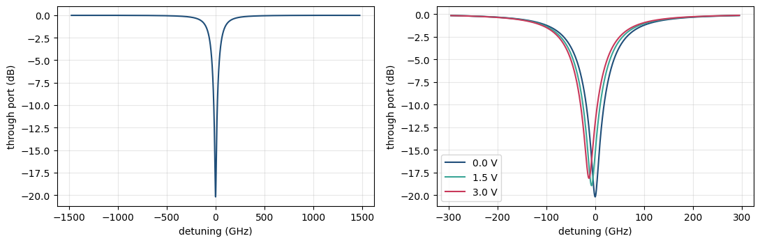
The resonance moves to lower frequency under reverse bias. Depleting the junction removes free carriers, free carriers lower the refractive index, so taking them away raises it and lengthens the optical path. The resonance also gets slightly shallower, because the absorption that was helping the ring reach critical coupling leaves with the same carriers.
The quantity that matters to the link is the extinction obtained at an acceptable insertion loss, so the operating point is read off a sweep of the laser detuning.
[16]:
# Find the best detuning and the extinction it gives, at the allowed loss
er_op, detune_op = extinction(ring_model, mrm, fsr)
print(f"operating point: laser {detune_op*1e-9:+.1f} GHz from the cold resonance")
print(f"  insertion loss {il_operating:.1f} dB, extinction {er_op:.2f} dB")

# Sweep a window around the resonance at both logic levels
freqs = f0 + np.linspace(-0.15, 0.15, 3001) * fsr

# Transmission with the junction unbiased, which is one logic level
ring_model.update(voltage=0.0)
dark = np.abs(mrm.s_matrix(freqs)[("P0@0", "P1@0")]) ** 2

# Transmission at full drive, which is the other
ring_model.update(voltage=v_drive)
bright = np.abs(mrm.s_matrix(freqs)[("P0@0", "P1@0")]) ** 2

# Return the model to zero bias before leaving the cell
ring_model.update(voltage=0.0)

fig, ax = plt.subplots(figsize=(6, 3.8))

# Plot the ratio of the two levels, which is the extinction the receiver sees
ax.plot(
    (freqs - f0) * 1e-9,
    10 * np.log10(np.maximum(bright, 1e-12) / np.maximum(dark, 1e-12)),
    color="#c8385a",
    label="extinction ratio",
)
# Plot the loss at the brighter level, which is what the link budget pays
ax.plot(
    (freqs - f0) * 1e-9,
    -10 * np.log10(np.maximum(bright, 1e-12)),
    color="#1f4e79",
    label="insertion loss",
)

# Mark the detuning the two curves together select
ax.axvline(detune_op * 1e-9, ls="--", c="0.5")
ax.set_xlabel("laser detuning from the cold resonance (GHz)")
ax.set_ylabel("dB")
ax.set_ylim(0, 12)
ax.legend()
ax.grid(alpha=0.3)
plt.tight_layout()
plt.show()
Progress: 100%
Progress: 100%
operating point: laser +32.4 GHz from the cold resonance
  insertion loss 4.0 dB, extinction 2.08 dB
Progress: 100%
Progress: 100%
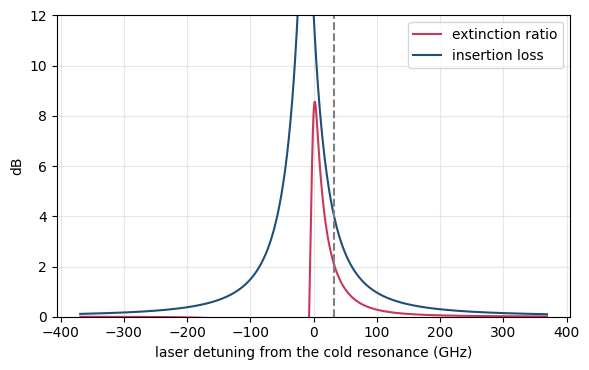
The small-signal bandwidth this ring reaches when biased on the flank is larger than the photon-lifetime figure quoted above, because the modulation sidebands beat against the cavity asymmetrically. Measuring that is a time-domain exercise, and the Optical Peaking in a Microring Modulator example shows how it is done. Link Simulation takes it up, where waveforms are already being driven through the ring.
The demultiplexer
On the receive side each channel is taken off a shared bus and sent to its own detector, which is an add-drop ring: two couplers instead of one, with the dropped light leaving on a second waveguide.
Two requirements act on the same quantity and pull in opposite directions. The filter has to pass a 100 Gb/s signal, which asks for a passband wider than the line rate. It also has to reject the neighbouring channel 200 GHz away, which asks for a passband narrower than the channel spacing. On a 200 GHz grid there is little room between the two, so the shape of the response matters as much as its width.
One ring is not enough. Its drop response is a Lorentzian, and a Lorentzian wide enough to carry 100 Gb/s is only a few dB down one channel away.
Two rings in series are not enough either, although they are the obvious next step. Cascading two add-drop rings multiplies their responses, which doubles the rejection in decibels and narrows the passband to 64 percent of one stage. The skirts still fall at a single ring’s rate, so every gigahertz of passband bought back costs the rejection it bought. The pair moves along the trade rather than escaping it.
Coupling the two rings to each other changes the order. In a series-coupled pair, light reaching the drop bus has passed through two resonances in succession rather than two independent ones, which makes the filter second order: its skirts fall twice as fast, so at equal rejection the passband is close to twice as wide. The condition for a flat passband, from Little’s coupled-mode treatment of ring channel-dropping filters, ties the two couplings together:
with \(\kappa_\text{ext}^2\) the bus-to-ring power coupling and \(\kappa_\text{int}^2\) the ring-to-ring one. The filter therefore has two couplings to measure, and the second follows from the first.
Two decisions come before both measurements.
The waveguide is strip, not rib. The modulator needs a rib because its junction has to reach its contacts, but these filters have no contacts to reach, and a slab wide enough to carry contacts also guides modes of its own for the coupler to excite.
The couplers are measured, and the round trip is assembled from those measurements. Driving the straight bus, this coupler conserves power to better than a part in a thousand, so both fractions it reports can be trusted: what crosses into the ring, and what stays on the bus. Driving the ring arc instead loses ten times as much, and that loss is an artifact of terminating a curved waveguide on a port rather than anything light does on a real ring.
Assembling the round trip
A ring model needs the round-trip field amplitude u, the factor multiplying the circulating field once per turn. Two effects reduce it.
The first factor covers both couplers of one ring. Each ring of the pair passes one bus coupler and one ring-to-ring coupler per turn, and each transmits a field \(\sqrt{T}\). For the bus coupler that is \(T_\text{ext}\), the through power the sweep measured, which is what puts its own loss into the round trip: whatever a coupler loses is already missing from what it transmits. For the ring-to-ring coupler the ideal value is used instead, for a reason given with its measurement below.
The second factor is propagation, over the round-trip length \(L\). The mode solver puts the radiation of a strip bend at this radius at zero, so what remains is sidewall scattering, which no solve predicts and which comes from process data.
pf.DualRingModel will not take u. It takes one propagation_loss per ring and applies the ideal coupler transmissions itself, so it has to be handed the loss that reproduces the same round trip:
\(\alpha_\text{eff}\) is therefore not the waveguide loss. It is an effective distributed loss carrying both the sidewall scattering and the couplers’ excess, spread over the round trip because the model accepts a single number. The cell prints both parts.
[17]:
strip_gap = 0.15  # Tightest gap the mask holds, um

line_rate = 100e9  # Line rate per channel, bit/s
target_fwhm = 1.4 * line_rate  # Filter passband target, Hz, set by the line rate

# Solve the strip bend mode, on a window wide enough to hold the radiating tail
strip_spec = tech.ports["TE_1550_500"].copy()
strip_spec.width, strip_spec.limits = 2 * r_target - 0.2, (-2.0, 2.0)

strip_spec.target_neff = 2.5  # Starting guess for the effective index
strip_modes = pf.port_modes(
    pf.Port((0, 0), 0, strip_spec, bend_radius=r_target),
    frequencies=[f0],
    group_index=True,
    technology=tech,
    verbose=False,
).data.modes_info

n_eff_strip = float(strip_modes["n eff"].isel(mode_index=0).item())
n_group_strip = float(strip_modes["group index"].isel(mode_index=0).item())
bend_loss_strip = max(float(strip_modes["loss (dB/cm)"].isel(mode_index=0).item()), 0.0)
print(
    f"strip bend at r = {r_target} um: n_eff {n_eff_strip:.4f}, "
    f"n_group {n_group_strip:.4f}, bend loss {bend_loss_strip:.5f} dB/cm"
)

# Add the bend loss and the sidewall scattering into one propagation loss
prop_loss_db_um = (bend_loss_strip + scattering_db_cm) * 1e-4
print(f"waveguide loss {(bend_loss_strip + scattering_db_cm):.1f} dB/cm\n")

# Build one bus coupler, re-evaluated below for each straight length
half_ring = pf.parametric.ring_coupler(
    port_spec="TE_1550_500",
    radius=r_target,
    coupling_distance=w_core + strip_gap,
    bus_length=5.0,
    coupling_length=0.0,
    euler_fraction=0.0,
    port_bends=True,  # arc-end ports carry the bend mode, not the straight one
    model=pf.Tidy3DModel(
        grid_spec=14,
        verbose=False,
        # Reuse the mirror symmetry, so P0 also gives P2's row
        port_symmetries=[("P2", "P3", "P0", "P1")],
    ),
)


def flat_pair(kappa_ext2, length, loss, n_eff, freqs):
    """Drop response of a maximally flat series-coupled pair."""
    # Set the ring to ring coupling from the flat-top condition above
    kappa_int2 = 0.5 * kappa_ext2**2
    model = pf.DualRingModel(
        kappa1=1j * np.sqrt(kappa_ext2),
        kappa2=1j * np.sqrt(kappa_int2),
        kappa3=1j * np.sqrt(kappa_ext2),
        n_eff1=n_eff,
        n_eff2=n_eff,
        length1=length,
        length2=length,
        propagation_loss1=loss,
        propagation_loss2=loss,
        n_group1=n_group_strip,
        n_group2=n_group_strip,
        reference_frequency=f0,
        ports=["P0", "P1", "P2", "P3"],
    )
    cell = model.black_box_component(port_spec="TE_1550_500")
    return np.abs(cell.s_matrix(freqs, show_progress=False)[("P0@0", "P2@0")]) ** 2


def shape_of(freqs, curve, spacing):
    """Band centre, the level there, the 3 dB width, and the rejection one
    channel away.

    A flat top has no meaningful peak: the highest point lands on whichever
    ripple happens to be higher, tens of gigahertz off centre. A channel sits
    at the centre of its band, so every level here is read from there.
    """
    i = int(np.argmax(curve))

    # Take everything above half the peak, close enough that no neighbour joins
    near = np.abs(freqs - freqs[i]) < 0.25 * (freqs[-1] - freqs[0])
    band = freqs[near][curve[near] >= 0.5 * curve[i]]
    centre = 0.5 * (band.min() + band.max())
    here = np.interp(centre, freqs, curve)

    # Take the worse neighbour, since a detuned band is not symmetric
    adjacent = max(np.interp(centre + s * spacing, freqs, curve) for s in (-1, 1))
    return centre, here, band.max() - band.min(), 10 * np.log10(here / adjacent)


print(
    f"{'L_c um':>7s} {'length um':>10s} {'kappa^2':>9s} {'sum':>8s} "
    f"{'FSR GHz':>9s} {'pair GHz':>9s} {'reject dB':>10s}"
)

# Sweep the straight coupling length and record what each one would give
candidates = {}
for lc in (0.0, 2.0, 4.0, 5.0, 6.0, 7.0):

    # Rebuild the same component at this straight length
    half_ring.update(coupling_length=lc)

    # Drive the straight bus alone, the one launch that conserves power here
    s = half_ring.s_matrix([f0], model_kwargs={"inputs": ["P0"]})

    # Read P0 to P3, which crosses into the ring, and P0 to P2, which does not
    kappa2 = float(np.abs(s[("P0@0", "P3@0")][0]) ** 2)
    through = float(np.abs(s[("P0@0", "P2@0")][0]) ** 2)

    # Add up the round trip: two half circles plus the two straights
    length = 2 * np.pi * r_target + 2 * lc
    # Name it for the sweep, so it does not shadow the modulator's own numbers
    fsr_lc = pf.C_0 / (n_group_strip * length)

    # Scan one free spectral range, with the index putting a resonance on the carrier
    freqs_lc = f0 + np.linspace(-0.5, 0.5, 801) * fsr_lc
    n_eff_lc = round(n_eff_strip * length / lda0) * lda0 / length

    # Work out what the coupled pair would give, which is what the link sees
    curve = flat_pair(kappa2, length, prop_loss_db_um, n_eff_lc, freqs_lc)
    _, _level, width_lc, reject_lc = shape_of(freqs_lc, curve, channel_grid)
    candidates[lc] = dict(
        kappa2=kappa2,
        through=through,
        length=length,
        fsr=fsr_lc,
        width=width_lc,
        reject=reject_lc,
        n_eff=n_eff_lc,
    )
    print(
        f"{lc:7.1f} {length:10.2f} {kappa2:9.4f} {kappa2 + through:8.4f} "
        f"{fsr_lc*1e-9:9.0f} {width_lc*1e-9:9.1f} {reject_lc:10.1f}"
    )

# Take the shortest straight whose passband still clears the target
clears = [lc for lc in candidates if candidates[lc]["width"] >= target_fwhm]
coupling_length = min(clears) if clears else max(candidates)
chosen = candidates[coupling_length]
kappa2_ext = chosen["kappa2"]
kappa2_int = 0.5 * kappa2_ext**2
drop_length, fsr_strip = chosen["length"], chosen["fsr"]
print()
print(
    f"chosen: {coupling_length:.1f} um of straight, bus coupling "
    f"{kappa2_ext:.4f}, passband {chosen['width']*1e-9:.0f} GHz against a "
    f"{target_fwhm*1e-9:.0f} GHz target"
)
print(f"the flat-top condition then asks for ring to ring {kappa2_int:.4f}")
Progress: 100%
strip bend at r = 5.0 um: n_eff 2.4452, n_group 4.1877, bend loss 0.00000 dB/cm
waveguide loss 2.0 dB/cm

 L_c um  length um   kappa^2      sum   FSR GHz  pair GHz  reject dB
Progress: 100%
    0.0      31.42    0.0182   0.9997      2279      11.4       61.0
Progress: 100%
    2.0      35.42    0.0727   0.9994      2021      45.5       39.1
Progress: 100%
    4.0      39.42    0.1596   0.9991      1816      90.8       26.9
Progress: 100%
    5.0      41.42    0.2133   0.9990      1729     116.7       22.5
Progress: 100%
    6.0      43.42    0.2721   0.9987      1649     140.2       18.7
Progress: 100%
    7.0      45.42    0.3358   0.9988      1576     169.5       15.5

chosen: 6.0 um of straight, bus coupling 0.2721, passband 140 GHz against a 140 GHz target
the flat-top condition then asks for ring to ring 0.0370
The sums in the fourth column are the reason to trust this table. A coupler that loses nothing sends everything to one of two places, so the coupled and the through fractions have to add to one. They do, to better than a part in a thousand, which says the FDTD is reporting the coupling and not its own numerical residue.
The alternative excitation is worse. Driving the same cell from the ring side, where the port sits on a curved waveguide, loses about one percent instead of one part in a thousand, and none of that loss is physical: the mode solver puts this bend’s loss at zero. Terminating a bend on a port costs about a hundredth of a dB in FDTD however the mesh is refined, and a resonator multiplies that by its finesse. A ring composed from arc-excited scattering matrices inherits the error four times per round trip and reports a drop loss several times the truth.
So the filter below takes its coupling from the measurement and its loss from the mode solver and the process, which is the combination each of those is good for.
The second coupling
The ring-to-ring coupler is the same straight section at a wider gap, between two waveguides that both curve away from it. It is weaker than the bus coupling by about a factor of eight here, so the gap that produces it is a few hundred nanometres rather than the tightest the mask can hold, which makes it the easier of the two to fabricate.
Only its coupling is taken from the measurement. Its through fraction is not, for the reason given above: both of its ports sit on curved waveguides, so it loses about half a percent to the port terminations rather than to anything physical. Half a percent per turn on a ring of this finesse would double the drop loss. The round trip therefore uses the ideal \(1 - \kappa_\text{int}^2\) here and keeps the measured through only for the bus coupler, whose straight-side excitation is trustworthy.
[18]:
def ring_ring_coupling(gap):
    """Power coupled between the two rings at one gap, from FDTD."""
    # Build the ring to ring coupler, whose two sides both curve away
    rr = pf.parametric.dual_ring_coupler(
        port_spec="TE_1550_500",
        coupling_distance=w_core + gap,
        radius=r_target,
        coupling_length=coupling_length,
        euler_fraction=0.0,
        port_bends=True,
        model=pf.Tidy3DModel(grid_spec=14, verbose=False),
    )
    s = rr.s_matrix([f0], model_kwargs={"inputs": ["P0"]})

    # Read P0 to P3, which crosses to the other ring, and P0 to P2, which stays
    return (
        float(np.abs(s[("P0@0", "P3@0")][0]) ** 2),
        float(np.abs(s[("P0@0", "P2@0")][0]) ** 2),
    )


# Try a few gaps between the rings, out where the coupling is weak
print(f"{'gap nm':>7s} {'kappa^2':>9s} {'through':>9s} {'sum':>8s}")
ring_coupling = {}
for gap in (0.25, 0.30, 0.35, 0.40):
    ring_coupling[gap] = ring_ring_coupling(gap)
    k2, th = ring_coupling[gap]
    print(f"{gap*1e3:7.0f} {k2:9.5f} {th:9.5f} {k2 + th:8.4f}")

# Fit log coupling against gap, then read off the gap the condition asks for
gaps = np.array(sorted(ring_coupling))
fit = np.polyfit(gaps, np.log([ring_coupling[g][0] for g in gaps]), 1)
ring_gap = round(float((np.log(kappa2_int) - fit[1]) / fit[0]), 3)
print()
print(
    f"the fit asks for {ring_gap*1e3:.0f} nm, "
    f"{-1e3*np.log(10)/fit[0]:.0f} nm per decade of coupling"
)

# Measure at that gap rather than trusting the fit
kappa2_int, through_int = ring_ring_coupling(ring_gap)
through_ext = chosen["through"]
print(f"which measures {kappa2_int:.4f} against {0.5*kappa2_ext**2:.4f} asked for")

# Build the round-trip amplitude from both couplers and the propagation loss
a_prop = 10 ** (-prop_loss_db_um * drop_length / 20)
u = np.sqrt(through_ext * (1 - kappa2_int)) * a_prop

# Divide the ideal coupler transmissions back out, since the model applies them
ideal = np.sqrt((1 - kappa2_ext) * (1 - kappa2_int))
ring_loss_db_um = -20 * np.log10(u / ideal) / drop_length

print()
print(
    f"effective ring loss {ring_loss_db_um * 1e4:.1f} dB/cm, of which the "
    f"waveguide is {bend_loss_strip + scattering_db_cm:.1f} and the bus "
    f"coupler the rest"
)
 gap nm   kappa^2   through      sum
Progress: 100%
    250   0.05057   0.94268   0.9933
Progress: 100%
    300   0.02194   0.97149   0.9934
Progress: 100%
    350   0.00961   0.98400   0.9936
Progress: 100%
    400   0.00420   0.98952   0.9937

the fit asks for 269 nm, 139 nm per decade of coupling
which measures 0.0367 against 0.0370 asked forProgress: 100%


effective ring loss 3.8 dB/cm, of which the waveguide is 2.0 and the bus coupler the rest
The filter as a placeable cell
The filter also has to exist as a cell the layout notebook can place: two racetracks stacked, a bus under the lower one and a bus over the upper one, and a heater on each ring, since a demultiplexer ring has to be trimmed onto its channel exactly as a modulator does.
Stacking the rings that close costs the heaters most of their width. Each loop reaches half a heater width outside its own ring, the two ring centres are only a ring gap more than two diameters apart, and the process holds 300 nm between heater features, so the widest loop that fits is 400 nm rather than the modulator’s 1200. A narrower heater over the same core is not a hardship: it concentrates the heat where the mode is and covers less of the waveguide with metal.
The two feeds leave in opposite directions, one down and one up, because a feed leaving the lower ring upwards would run straight into the upper ring. Each crosses the bus beneath it on the heater layer, which sits above the core, and is what the modulator’s feed already does.
Which end of the drop bus the light leaves from has to be worked out, not assumed, and with two rings the answer is the opposite of the one-ring case.
A directional coupler is co-directional: light crossing from one waveguide to the other keeps travelling the same way. pf.parametric.ring_coupler shows it in its own port coordinates, with the bus input at one end and the port it couples into at the far end of the ring arc. A half turn of a ring does reverse the direction. So the side the drop leaves on is decided by how many half turns the light takes on the way through: one ring is one half turn and the drop comes out on the far side,
two rings are two half turns and it comes out on the same side as the through port.
An analytic model cannot catch an error here. pf.DualRingModel is told which of its four port names is the drop and obeys that, wherever the port sits on the mask, so a filter with the label on the wrong end simulates correctly and is dark on a probe station. The cell below prints both port positions as a check.
[19]:
@pf.parametric_component(name_prefix="DROP2R")
def two_ring_filter(
    *,
    ring_radius=5.0,
    core_width=0.5,
    bus_gap=0.15,
    ring_gap=0.32,
    coupling_length=6.0,
    heater_width=0.4,  # Narrower than the modulator's, so the two clear each other
    heater_slot=0.35,
    heater_reach=3.0,
    bus_length=16.0,
    kappa_ext=0.5,
    kappa_int=0.177,
    n_eff=2.4,
    n_group=4.2,
    propagation_loss=2.0e-4,
    dn_dT=0.0,
    temperature=293.0,  # Both rings sit at the same temperature
):
    # Leave the name empty, so each channel's filter becomes its own cell
    c = pf.Component()

    # Halve the coupling length, since the straights run either side of the origin
    r, half_lc = ring_radius, coupling_length / 2

    # Set the outer and inner edges of the ring core
    outer, inner = r + core_width / 2, r - core_width / 2

    # Place the two ring centres, facing each other across the ring gap
    y_ring = (0.0, 2 * r + core_width + ring_gap)

    # Set the gap between the two heater terminals, which straddle the slot
    terminal_gap = 3.0
    terminal_x = (metal_width + terminal_gap) / 2

    # Widen the feed to hold both terminals, their vias and half a heater width
    feed_wide = 2 * (terminal_x + metal_width / 2) + heater_width / 2

    # Set the outer and inner edges of the heater, on the same racetrack
    h_out, h_in = r + heater_width / 2, r - heater_width / 2

    # Widen the taper so the slot leaves an arm of a heater width either side
    taper_wide = heater_slot + 2 * heater_width

    def racetrack(y0, sign):
        """One ring and its heater, with the feed leaving on the given side."""
        # Draw the racetrack core, two half circles joined by two straights
        c.add(
            "Si",
            pf.Circle(
                outer, center=(half_lc, y0), inner_radius=inner, sector=(-90, 90)
            ),
            pf.Circle(
                outer, center=(-half_lc, y0), inner_radius=inner, sector=(90, 270)
            ),
            pf.Rectangle((-half_lc, y0 - outer), (half_lc, y0 - inner)),
            pf.Rectangle((-half_lc, y0 + inner), (half_lc, y0 + outer)),
        )

        # Set the height the heater feed leaves at, clear of the ring
        feed_end = y0 + sign * (r + heater_reach)

        # Cut one slot through the heater loop and its feed, leaving one conductor
        c.add(
            "Heater",
            *pf.boolean(
                [
                    pf.Circle(
                        h_out, center=(half_lc, y0), inner_radius=h_in, sector=(-90, 90)
                    ),
                    pf.Circle(
                        h_out,
                        center=(-half_lc, y0),
                        inner_radius=h_in,
                        sector=(90, 270),
                    ),
                    pf.Rectangle((-half_lc, y0 - h_out), (half_lc, y0 - h_in)),
                    pf.Rectangle((-half_lc, y0 + h_in), (half_lc, y0 + h_out)),
                    # Start the flare a taper width clear of the loop
                    pf.Path((0, feed_end), feed_wide)
                    .segment((0, feed_end - sign * heater_width), feed_wide)
                    .segment((0, y0 + sign * (h_out + taper_wide)), taper_wide)
                    .segment((0, y0 + sign * r), taper_wide),
                ],
                [pf.Path((0, feed_end + sign * 0.5), heater_slot).segment((0, y0))],
                "-",
            ),
        )
        return feed_end

    # Feed the lower ring downwards and the upper ring upwards, so they never meet
    feeds = [racetrack(y_ring[0], -1), racetrack(y_ring[1], 1)]

    # Take the strip port spec, since the filters carry no junction
    port_spec = pf.config.default_technology.ports["TE_1550_500"]

    # Offset each bus from its ring centre by the radius, a core and the gap
    offset = r + core_width + bus_gap
    y_in, y_drop = y_ring[0] - offset, y_ring[1] + offset

    # Draw one bus under the lower ring and one over the upper ring
    for y in (y_in, y_drop):
        c.add(
            "Si",
            pf.Rectangle(
                (-bus_length / 2, y - core_width / 2),
                (bus_length / 2, y + core_width / 2),
            ),
        )

    # Add the four optical ports, with the drop directly above the through port
    c.add_port(pf.Port((-bus_length / 2, y_in), 0, port_spec), "in")
    c.add_port(pf.Port((bus_length / 2, y_in), 180, port_spec), "thru")
    c.add_port(pf.Port((bus_length / 2, y_drop), 180, port_spec), "drop")
    c.add_port(pf.Port((-bus_length / 2, y_drop), 0, port_spec), "add")

    # Add the heater terminals, each ring's pair leaving on its own side
    for feed_end, sign, tags in zip(feeds, (-1, 1), (("H0A", "H1A"), ("H0B", "H1B"))):
        for name, side in zip(tags, (-1, 1)):
            box = pf.Rectangle(
                center=(side * terminal_x, feed_end - sign * 0.6),
                size=(metal_width, metal_width),
            )
            c.add("Via", box)
            c.add_terminal(pf.Terminal("M1", box), name)

    # Round-trip length of each ring: the circle plus the two straights
    length = 2 * np.pi * r + 2 * coupling_length

    # Series-coupled pair: bus to ring one, ring one to ring two, ring two to bus
    model = pf.DualRingModel(
        kappa1=1j * kappa_ext,
        kappa2=1j * kappa_int,
        kappa3=1j * kappa_ext,
        n_eff1=n_eff,
        n_eff2=n_eff,
        length1=length,
        length2=length,
        propagation_loss1=propagation_loss,
        propagation_loss2=propagation_loss,
        n_group1=n_group,
        n_group2=n_group,
        reference_frequency=f0,
        dn1_dT=dn_dT,
        dn2_dT=dn_dT,
        temperature1=temperature,
        temperature2=temperature,
        reference_temperature=293.0,
        ports=["in", "thru", "drop", "add"],
    )

    # Raise the pole count, since two coupled rings put several resonances in band
    model.time_stepper = pf.SMatrixTimeStepper(min_poles=8, max_poles=20)
    c.add_model(model, "dual ring")
    return c


# Round the index to put a resonance on the carrier at the nominal length
n_eff_drop = round(n_eff_strip * drop_length / lda0) * lda0 / drop_length

second_order = two_ring_filter(
    ring_radius=r_target,
    bus_gap=strip_gap,
    ring_gap=ring_gap,
    coupling_length=coupling_length,
    kappa_ext=np.sqrt(kappa2_ext),
    kappa_int=np.sqrt(kappa2_int),
    n_eff=n_eff_drop,
    n_group=n_group_strip,
    propagation_loss=ring_loss_db_um,
    dn_dT=dn_eff_dt,
)

# Print both port positions, which is the only check on which side the drop leaves
print(
    f"through port at x {second_order.ports['thru'].center[0]:+.1f} um, "
    f"drop at x {second_order.ports['drop'].center[0]:+.1f} um"
)

# Work out the clearance between the two heater loops, which sets their width
heater_clearance = (
    2 * r_target
    + w_core
    + ring_gap
    - 2 * (r_target + second_order.parametric_kwargs["heater_width"] / 2)
)
print(f"heater loops clear each other by {heater_clearance*1e3:.0f} nm")

# Scan one free spectral range, which holds one resonance
strip_freqs = f0 + np.linspace(-0.5, 0.5, 1601) * fsr_strip
check = second_order.s_matrix(strip_freqs)
on_resonance = int(np.argmin(np.abs(strip_freqs - f0)))
for key, label in ((("in@0", "drop@0"), "drop"), (("in@0", "thru@0"), "through")):
    print(f"{label:8s} port at resonance: {np.abs(check[key][on_resonance])**2:.4f}")
viewer(second_order)
through port at x +8.0 um, drop at x +8.0 um
heater loops clear each other by 369 nm
drop     port at resonance: 0.9427
through  port at resonance: 0.0381
Progress: 100%
[19]:

The response below is what the second order buys. The passband is flat across its top rather than peaked, so a modulated signal passes without being tilted, and the skirts fall steeply enough that the neighbouring channel is still well rejected at nearly twice the width a cascade of two single rings could offer.
Both numbers are read at the centre of the band, which is where the channel sits. A flat top has no single peak worth quoting: its highest point lands on whichever ripple happens to be higher, tens of gigahertz off centre, and reading the loss and the rejection from there would flatter both.
[20]:
# Measure the pair's drop response, then one ring's for comparison
pair = np.abs(second_order.s_matrix(strip_freqs)[("in@0", "drop@0")]) ** 2

# Build one ring at the same bus coupling, the filter this design replaced
single = pf.RingModel(
    kappa1=1j * np.sqrt(kappa2_ext),
    kappa2=1j * np.sqrt(kappa2_ext),
    n_eff=n_eff_drop,
    n_group=n_group_strip,
    length=drop_length,
    propagation_loss=ring_loss_db_um,
    reference_frequency=f0,
    ports=["P0", "P1", "P2", "P3"],
).black_box_component(port_spec="TE_1550_500")
one = np.abs(single.s_matrix(strip_freqs)[("P0@0", "P2@0")]) ** 2

fig, ax = plt.subplots(figsize=(6, 3.6))
for curve, label, color in (
    (one, "one ring", "#1f4e79"),
    (pair, "two coupled rings", "#3aa596"),
):

    # Read both with the same interpolation, so the comparison is like for like
    _, level, width, reject = shape_of(strip_freqs, curve, channel_grid)
    print(
        f"{label:18s} passband {width*1e-9:6.1f} GHz, "
        f"drop loss {-10*np.log10(level):5.2f} dB, "
        f"crosstalk {-reject:6.1f} dB"
    )
    ax.plot(
        (strip_freqs - f0) * 1e-9,
        10 * np.log10(curve / curve.max()),
        color=color,
        label=label,
    )
for offset in (-channel_grid, channel_grid):
    ax.axvline(offset * 1e-9, ls="--", c="#c8385a", lw=1)

# Shade the band a 100 Gb/s signal occupies, which is what has to fit
ax.axvspan(
    -line_rate * 1e-9 / 2,
    line_rate * 1e-9 / 2,
    color="tab:orange",
    alpha=0.18,
    label=f"{line_rate*1e-9:.0f} Gb/s signal",
)
ax.set_xlabel("detuning (GHz)")
ax.set_ylabel("drop port, normalised (dB)")
ax.set_xlim(-500, 500)
ax.set_ylim(-45, 2)
ax.legend(fontsize=8)
ax.grid(alpha=0.3)
plt.tight_layout()
plt.show()
Progress: 100%
Progress: 100%
one ring           passband  169.0 GHz, drop loss  0.05 dB, crosstalk   -8.0 dB
two coupled rings  passband  142.2 GHz, drop loss  0.26 dB, crosstalk  -18.7 dB
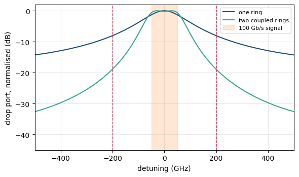
Landing each ring on its own channel
Eight channels 200 GHz apart span 1400 GHz, and every ring so far is identical. Something has to put each one on its own channel, and the heater is the obvious candidate because it is already there. It is worth checking whether it can actually do it before assuming so.
[21]:
# Use the strip group index here, since the filter is a strip waveguide
ghz_per_k_strip = f0 * dn_eff_dt / n_group_strip * 1e-9

print(f"channel span      {channel_span*1e-9:.0f} GHz across {n_channels} channels")
print(
    f"heater tuning     {ghz_per_k_strip:.2f} GHz/K on the filter, "
    f"{ghz_per_k_rib:.2f} on the modulator"
)
print(f"needed to span it {channel_span*1e-9 / ghz_per_k_strip:.0f} K on the last ring")

# Convert one channel of detuning into the round-trip length that produces it
dl_per_channel = drop_length * channel_grid / f0
print()
print(f"or {dl_per_channel*1e3:.0f} nm of extra round trip per channel")
print(f"which is {dl_per_channel/2*1e3:.0f} nm on each of the two straight sections")

# Report what the heater is left to do, which is drift rather than spacing
print()
print(f"trimming +-50 GHz needs {50/ghz_per_k_strip:.1f} K")
channel span      1400 GHz across 8 channels
heater tuning     8.62 GHz/K on the filter, 9.31 on the modulator
needed to span it 162 K on the last ring

or 45 nm of extra round trip per channel
which is 22 nm on each of the two straight sections

trimming +-50 GHz needs 5.8 K
The heater cannot do it. Spanning the grid would take well over a hundred kelvin on the last ring, which is neither reliable nor affordable in power, and it would put the outer rings far enough above ambient that they drift with everything around them.
So the channel spacing is built into the geometry instead. A resonance follows the round trip through df/f = -dL/L, so one channel of detuning is one channel’s worth of length: a few tens of nanometres, split between the two straight sections of the racetrack. That is a change the mask can hold, and it barely touches the coupling, because a few tens of nanometres on a several-micron straight is a fraction of a percent.
The racetrack earns its place twice over here. In a plain circular ring the same detuning has to come out of the radius, which is a much smaller step and moves the bend loss and the coupling gap with it. In a racetrack it is just the straight section, which changes the path length and nothing else.
The heater then does what it is good at: trimming out fabrication drift and holding the ring against temperature, tens of GHz rather than thousands, which is a few kelvin.
The rib to strip transition
Only the modulator is rib, so its bus has to meet the strip circuit at both ends. Both port specifications already carry the same 500 nm core, so the core runs straight through and the transition is nothing more than the slab going away.
pf.parametric.transition builds it by interpolating between the two specifications. The strip specification has no slab entry, so by default the slab narrows to zero width and the cell ends in a point, which the minimum-width rule in Chip Layout rejects. The min_width argument stops the slab at a width the process can hold instead.
A constant_length of one micron at each end keeps the port planes clear of the taper: the last micron is plain strip, so the mode at the port is the strip mode and nothing else. The cost of ending a slab abruptly rather than infinitely gradually is measured below, against the same FDTD model, so the trade is visible rather than assumed.
[22]:
# Take both port specs, which share a core and differ only in the slab
rib_spec, strip_spec = tech.ports["Rib_TE_1550_500"], tech.ports["TE_1550_500"]

# Taper the slab over 8 um and end it square at 400 nm, above the 300 nm the process holds.
# One micron of constant cross-section at each end makes 10 um from rib port to strip port,
# with plain strip in the last micron.
rib_to_strip = pf.parametric.transition(
    port_spec1=rib_spec,
    port_spec2=strip_spec,
    length=8.0,
    constant_length=1.0,
    min_width=0.4,
    name="rib_to_strip",
    model=pf.Tidy3DModel(grid_spec=12, verbose=False),
)
# Solve five points across 8 THz, enough to see whether the taper is dispersive
s_tr = rib_to_strip.s_matrix(f0 + np.linspace(-4e12, 4e12, 5))
print(f"insertion loss {-10*np.log10(np.abs(s_tr[('P0@0', 'P1@0')])**2).max():.3f} dB")
print(f"return loss    {10*np.log10(np.abs(s_tr[('P0@0', 'P0@0')])**2).max():.1f} dB")

# Replace the FDTD model with the two numbers it just produced
mid = len(s_tr[("P0@0", "P1@0")]) // 2  # the sample at the carrier
rib_to_strip.add_model(
    pf.TwoPortModel(
        t=complex(s_tr[("P0@0", "P1@0")][mid]),
        r0=complex(s_tr[("P0@0", "P0@0")][mid]),
        r1=complex(s_tr[("P1@0", "P1@0")][mid]),
        ports=["P0", "P1"],
    ),
    "compact",
)
print(f"active model now {rib_to_strip.active_model_name}")
viewer(rib_to_strip)
Progress: 100%
insertion loss 0.013 dB
return loss    -48.7 dB
active model now compact
[22]:

The detector and the edge coupler
The two remaining blocks are drawn here but not simulated, because their behaviour in the link is captured by a compact model and the physics behind each already has a worked example.
The germanium photodiode is a waveguide-coupled diode: light runs under a germanium block grown on the silicon and is absorbed over a few tens of microns. What the link needs from it is a responsivity, a bandwidth and a noise level, which is what the abstract photodiode block carries.
The edge coupler is an inverse taper narrowing to a tip at the chip facet. Its coupling efficiency to a lensed fiber is a facet property that depends on the tip width, the cladding and the fiber mode, and the Edge Coupler example works through simulating exactly that. Here the geometry is kept and the simulation skipped: the facet enters the link budget as a fixed insertion loss, which is what an analytic model of it amounts to.
[23]:
@pf.parametric_component(name_prefix="PD")
def germanium_photodiode(
    *,
    length=25.0,
    ge_width=2.0,
    taper_length=10.0,
    responsivity=0.9,
    bandwidth=60e9,
    dark_current=10e-9,
    gain=1e3,  # Transimpedance of the amplifier the diode drives, V/A
):
    # Leave the name empty, so the decorator builds one from the arguments
    c = pf.Component()

    # Take the strip port, since the detector is fed from the strip bus
    port_spec = pf.config.default_technology.ports["TE_1550_500"]

    # Widen the silicon under the germanium, so the mode transfers gradually
    c.add(
        "Si",
        pf.Path((-taper_length, 0), 0.5)
        .segment((0, 0), width=ge_width)
        .segment((length, 0)),
        # Add the germanium, which absorbs the light and makes the photocurrent
        "Ge",
        pf.Rectangle((0, -ge_width / 2), (length - 2, ge_width / 2)),
        # Reach the slab out to the contact strip beside the waveguide
        "Si Slab",
        pf.Rectangle((-taper_length, -3.0), (length, ge_width / 2)),
        # Add the ohmic implant and its plug, which take the anode out
        "Si p++",
        pf.Rectangle((-taper_length, -3.0), (length, -1.2)),
        "Contact",
        pf.Rectangle((-taper_length + 1, -2.8), (length - 1, -1.5)),
        # Add the cathode contact on top of the germanium
        "Ge Contact",
        pf.Rectangle((2, -0.5), (length - 4, 0.5)),
    )

    # Add the optical input at the narrow end of the silicon taper
    c.add_port(pf.Port((-taper_length, 0), 0, port_spec), "P0")
    # Take the photocurrent out on an electrical port, which a stepper can read
    c.add_port(
        pf.Port((length, 0), 0, virtual_port_spec(classification="electrical")), "E0"
    )
    for name, y, sign in (("ANODE", -2.15, -1.0), ("CATHODE", 0.0, 1.0)):
        c.add_terminal(
            pf.Terminal(
                "M1",
                pf.Rectangle(
                    center=(length / 2 + sign * metal_width, y), size=(metal_width, 1.0)
                ),
            ),
            name,
            add_structure=True,
        )
    # Graft the abstract photodiode's two models onto this drawn cell
    abstract_pd = pfa.photodiode(
        responsivity=responsivity,
        gain=gain,
        dark_current=dark_current,
        filter_frequency=bandwidth,
    )
    c.add_model(abstract_pd.models["Termination"], "pd", "optical")
    c.add_model(
        abstract_pd.models["Termination (electrical)"], "pd_electrical", "electrical"
    )
    return c


@pf.parametric_component(name_prefix="EC")
def edge_coupler(*, length=150.0, tip_width=0.18, insertion_loss=1.5):
    c = pf.Component()
    port_spec = pf.config.default_technology.ports["TE_1550_500"]
    # Narrow the silicon to an inverse taper, so the mode expands into the oxide
    c.add(
        "Si",
        pf.Path((0, 0), tip_width).segment((length, 0), width=0.5),
    )
    c.add_port(pf.Port((0, 0), 0, port_spec), "P0")
    c.add_port(pf.Port((length, 0), 180, port_spec), "P1")
    c.add_model(pfa.edge_coupler(insertion_loss=insertion_loss).active_model, "facet")
    return c


pd = germanium_photodiode()
ec = edge_coupler()
print("photodiode ports:", list(pd.ports), "terminals:", list(pd.terminals))
print("edge coupler ports:", list(ec.ports))
viewer(pd)
photodiode ports: ['E0', 'P0'] terminals: ['ANODE', 'CATHODE']
edge coupler ports: ['P0', 'P1']
[23]:

The monitor tap
Every photodiode so far is on the receive side, at the far end of a fibre. The transmitter cannot see its own output, and it has to: eight rings have to be held on eight channels, and tuning something you cannot measure is a guess rather than a control problem.
One weak coupler on the transmit bus fixes that, lifting a small fraction of the light onto a monitor diode.
One tap serves all eight channels. A tap is not wavelength selective, so its diode carries the whole comb at once. The channels are separated in the electronics rather than in the layout: each heater carries a small tone at its own frequency, and a lock-in at that frequency recovers that channel alone. What keeps the tones from mixing is that the rings are thermally independent, which Wavelength Plan and Thermal Budget measures at one part in ten thousand.
The coupling strength has wide tolerance. The tap costs the link whatever it removes, favouring a small value, while the diode needs current, favouring a large one. At one percent the link pays 0.04 dB and the monitor receives over a hundred microamps, so both limits are decades away.
The gap follows the same exponential the bus coupler did, further out on the tail: coupling falls about tenfold per 200 nm here. Only the tap arm bends, so the bus the eight modulators sit on stays straight.
It is drawn in strip, not rib. A rib waveguide carries a slab that reaches well past its core, so two ribs a few hundred nanometres apart leave slab slivers narrower than any process will hold. Strip has no slab to pinch, and the transmit bank already ends in a rib-to-strip transition, so the tap goes on the far side of it where the waveguide is strip anyway. That also matches the monitor diode, whose input was drawn in strip.
[24]:
tap_gap = 0.25  # Bus to tap gap, um, out on the evanescent tail

tap = pf.parametric.s_bend_straight_coupler(
    port_spec="TE_1550_500",
    coupling_distance=w_core + tap_gap,
    s_bend_length=12.0,
    # Offset enough to clear the bus for the route to the monitor diode
    s_bend_offset=6.0,
    coupling_length=0.0,
    euler_fraction=0.5,
    model=pf.Tidy3DModel(grid_spec=14, verbose=False),
)

# Read the four coefficients: P0 and P2 the bus, P3 the tap, P1 isolated
s_tap = tap.s_matrix([f0], model_kwargs={"inputs": ["P0"]}, show_progress=False)
coef = {k: complex(s_tap[("P0@0", f"{k}@0")][0]) for k in ("P0", "P1", "P2", "P3")}

print(f"tapped      {abs(coef['P3'])**2*100:.2f} percent")
print(f"bus loss    {-10*np.log10(abs(coef['P2'])**2):.3f} dB")
print(f"isolation   {abs(coef['P1'])**2:.1e}")
print(f"reflection  {abs(coef['P0'])**2:.1e}")

# Rotate the coupled amplitude into quadrature, where a lossless coupler puts it
c_quad = abs(coef["P3"]) * coef["P2"] / abs(coef["P2"]) * -1j
print(f"cross arm rotated by {np.angle(c_quad / coef['P3'], deg=True):+.1f} degrees")

# Replace FDTD with the four numbers it just produced
tap.add_model(
    pf.DirectionalCouplerModel(
        # Zero the isolated and reflected fractions, which sit at the noise floor
        t=coef["P2"],
        c=c_quad,
        i=0,
        r=0,
        ports=["P0", "P1", "P2", "P3"],
    ),
    "compact",
)

# Check the largest singular value of the compact model, which must not exceed one
s_c = tap.s_matrix([f0], show_progress=False)
names = ["P0", "P1", "P2", "P3"]
matrix = np.array([[s_c[(f"{a}@0", f"{b}@0")][0] for b in names] for a in names])
print(f"largest singular value {np.linalg.svd(matrix, compute_uv=False)[0]:.4f}")
print(f"active model now {tap.active_model_name}")
viewer(tap)
tapped      1.08 percent
bus loss    0.050 dB
isolation   1.6e-06
reflection  1.9e-08
cross arm rotated by +32.0 degrees
largest singular value 0.9996
active model now compact
[24]:

The rotation applied to the coupled amplitude is worth a paragraph, because leaving it out is a silent error rather than a visible one.
A directional coupler that loses nothing has to send its transmitted and coupled amplitudes out exactly 90 degrees apart. That is not a modelling convention but a consequence of power conservation, and DirectionalCouplerModel builds a four port that assumes it. The measured pair are 122 degrees apart instead, because the coupled arm leaves on an S bend and the transmitted arm runs straight, so the two paths are not the same length.
That extra length is real, but it belongs to the tap arm, and the compact model has one phase to describe both arms. Handed the measured pair, its S matrix has a largest singular value of 1.05: it creates power at one input combination and destroys it at another. A frequency-domain sweep barely notices. A time-domain circuit does, because it fits poles to that matrix, and the fit of a non-passive target settles about 0.23 dB low on the bus and 25 percent low on the tap.
Rotating the coupled amplitude into quadrature keeps every measured magnitude and the measured through phase, and discards only the tap arm’s excess path length, which nothing downstream of the monitor diode can see.
The bond pad
The last cell in the library is the one every electrical net ends on. A terminal on its own is a declaration, not a shape: it says where a net can be reached and on which layer, and it draws nothing. add_structure=True is what also lays the metal down, which is what a pad has to be.
The opening in the passivation is drawn smaller than the metal, so the probe lands on metal with an oxide rim around it rather than on the edge of it.
[25]:
# Draw 50 um of metal, which is what a probe tip or a wire bond lands on
bp = pf.Component("BondPad")

# Draw the metal as well as declaring the terminal, so there is something to land on
bp.add_terminal(pf.Terminal("M1", pf.Rectangle(size=(50, 50))), add_structure=True)

# Open the passivation 45 um across, leaving a 2.5 um rim of covered metal
bp.add("Pad Open", pf.Rectangle(size=(45, 45)))
viewer(bp)
[25]:

The library
Component |
Chosen by |
Value |
|---|---|---|
Ring radius |
clear of the bend-loss knee, with free spectral range to spare |
5 um |
Junction implants |
bandwidth, which a ring buys with loss rather than with coupling |
8e18 / 5e18 cm^-3 |
Modulator coupling |
1.2 times critical, trading a little depth for linewidth |
kappa^2 0.148 at a 123 nm gap |
Drive |
what a driver delivers into 50 ohm |
3 V peak to peak |
Demux filter |
the data rate first, then the neighbouring channel |
two coupled strip racetracks, 142 GHz wide |
Rib to strip transition |
the modulator is the only rib block |
10 um, slab ends at 400 nm |
Photodiode |
link budget |
0.9 A/W, 60 GHz |
Monitor tap |
small enough to ignore, large enough to read |
1 percent at a 250 nm gap |
Edge coupler |
facet, taken as a fixed loss |
1.5 dB |
Bond pad |
what a probe tip lands on |
50 um of metal |
Every optical number here came out of a solve on the technology from Technology and PDK Setup, and each cell carries the model that reproduces it, so they can be placed and simulated as they are.
Chip Layout does the placing. It builds the transmit bank of eight modulators on one bus, the receive bank of drop filters, and the metal that takes every heater and junction terminal out to its own bond pad, then runs design rule checks on the finished mask.