
Custom Component Library

This notebook defines a comprehensive library of parameterized photonic components used in the layout and simulation of our quantum chip. Utilizing photonforge alongside the SiEPIC technology setup, we programmatically generate the layout geometries, routing, and physical properties for each device.
Key components designed and simulated in this library include:
Basic Routing: Straight waveguides and bends.
Phase Control: Thermo-optic phase shifters for active tuning.
Interference & Splitting: 2x2 Multi-Mode Interferometers (MMIs) and adiabatic waveguide crossings.
Advanced Structures: Tunable Mach-Zehnder Interferometers (MZIs) and Asymmetric MZIs (AMZIs) for precise signal/idler routing.
I/O Interfaces: Grating couplers for fiber-to-chip light coupling.
Beyond just the physical layout, each component is coupled with an analytic or full-wave 3D electromagnetic simulation model (via Tidy3D). This allows us to compute their scattering matrices (S-matrices) across target telecommunication wavelengths (~1550 nm) and extract key performance metrics like transmission, crosstalk, and optimal thermal operating points before full-system integration.
References
Wang, Jianwei, et al. “Multidimensional quantum entanglement with large-scale integrated optics.” Science 2018 360 (6386), 285-291, doi: 10.1126/science.aar7053.
Ma et al. “Ultralow loss single layer submicron silicon waveguide crossing for SOI optical interconnect,” Opt Express, 2023 21 (24), 29374–29382, doi: 10.1364/OE.21.029374.
Guan, Hang, et al. “Compact and low loss 90° optical hybrid on a silicon-on-insulator platform.” Optics Express 2017 25 (23), 28957-28968, doi: 10.1364/OE.25.028957.
[1]:
import matplotlib.pyplot as plt
import numpy as np
import photonforge as pf
import photonforge.typing as pft
import siepic_forge as siepic
from photonforge.live_viewer import LiveViewer
from scipy.interpolate import make_interp_spline
from scipy.interpolate import interp1d

viewer = LiveViewer()
07:24:58 -03 WARNING: The material-library variant 'Palik_Lossless' is
             deprecated and maps to 'Palik_LowLoss' because it contains a tiny
             fitted loss despite its name. Use 'Palik_NoLoss' where available
             for a zero-loss Palik model.
LiveViewer started at http://localhost:45443
Technology Initialization and Port Setup
Before creating any components, we must define the physical constraints of our photonic platform. This cell initializes the SiEPIC EBeam technology stack, specifying the thicknesses of the Silicon-on-Insulator (SOI) layers: a 260 nm silicon core surrounded by 1 µm oxide layers.
We also define a standard PortSpec for a 450 nm wide strip waveguide. This ensures all generated components share a consistent optical interface, specifically optimized for the fundamental Transverse Electric (TE) mode at 1550 nm. Finally, we set global defaults in photonforge to streamline routing parameters, such as the default bend radius.
[2]:
# Initialize the SiEPIC EBeam technology with our specific SOI layer thicknesses (in microns)
tech = siepic.ebeam(
    si_thickness=0.26,
    bottom_oxide_thickness=1.0,
    top_oxide_thickness=1.0,
)

# Set this technology as the global default for all subsequent photonforge components
pf.config.default_technology = tech

# Default bend radius
bend_radius = 10.0

# Configure default arguments for routing to avoid repeating them in every component call
pf.config.default_kwargs = {
    "port_spec": "TE_1550_450",
    "radius": bend_radius,
}

# Define a custom optical port specification for a standard 450 nm wide strip waveguide
strip_spec = pf.PortSpec(
    description="Strip TE 1550 nm, w=450 nm",
    width=2,
    limits=(-0.99, 1.25),
    num_modes=1,
    added_solver_modes=0,
    polarization="",
    target_neff=3.5,
    path_profiles=[(0.45, 0, (1, 0))],
)

# Register the custom port specification to our technology setup
tech.add_port("TE_1550_450", strip_spec)
[2]:
Layers
| Name | Layer | Description | Color | Pattern |
|---|---|---|---|---|
| Si | (1, 0) | SiEPIC - Waveguide | #ff80a818 | \\ |
| PinRec | (1, 10) | SiEPIC | #ff80a818 | xx |
| PinRecM | (1, 11) | SiEPIC | #80000018 | + |
| Si Slab | (2, 0) | Dedicated Run Layers - Device…… Layer Partial Etch | #c080ff18 | / |
| Direct Metal | (5, 0) | Dedicated Run Layers | #80a8ff18 | || |
| Oxide open to BOX | (6, 0) | Dedicated Run Layers | #ff000018 | - |
| Text | (10, 0) | Text-Not Fabricated | #00000018 | hollow |
| M1_heater | (11, 0) | TiW Heater | #0000ff18 | \\ |
| M2_router | (12, 0) | TiW/Au Routing Bilayer | #ffbf0018 | // |
| M_Open | (13, 0) | Bond Pad Open | #80005718 | \\ |
| Si n | (20, 0) | Dedicated Run Layers | #afff8018 | - |
| Si p | (21, 0) | Dedicated Run Layers | #ffd9df18 | = |
| Si n+ | (22, 0) | Dedicated Run Layers | #ff800018 | x |
| Si p+ | (23, 0) | Dedicated Run Layers | #ddff0018 | xx |
| Si n++ | (24, 0) | Dedicated Run Layers | #00ffff18 | + |
| Si p++ | (25, 0) | Dedicated Run Layers | #00800018 | ++ |
| ANT Reserved | (31, 0) | SiEPIC/ANT Reserved | #9580ff18 | / |
| ANT Reserved 1 | (33, 0) | ANT Reserved | #9580ff18 | / |
| Via to silicon | (40, 0) | Dedicated Run Layers | #0000ff18 | . |
| DevRec | (68, 0) | SiEPIC | #00800018 | . |
| FbrTgt | (81, 0) | SiEPIC/Dedicated Run Layers | #80808018 | ++ |
| ANT Reserved 2 | (102, 0) | ANT Reserved | #9580ff18 | / |
| ANT Reserved 3 | (110, 0) | ANT Reserved | #9580ff18 | / |
| Custom Dicing | (189, 0) | #00000018 | hollow | |
| SEM Imaging | (200, 0) | #ff000018 | x | |
| Deep Trench | (201, 0) | #00ff0018 | . | |
| Deep Trench Handling Exclusion | (202, 0) | #00760018 | : | |
| Thermal Isolation Trenches | (203, 0) | #00800018 | \ | |
| Laser Integration Shelf | (205, 0) | Dedicated Run Layers | #69ff0518 | xx |
| Floor Plan-Not Fabricated | (290, 0) | #c080ff18 | hollow | |
Error: device layer width is…… less than design rule | (301, 0) | DRC Errors | #80005718 | = |
Error: device layer spacing is…… less than design rule | (301, 1) | DRC Errors | #80005718 | - |
Warning: polygons/paths on…… PinRec layer (1/10) will NOT be fabricated | (301, 2) | DRC Errors | #80005718 | || |
Error: direct metal width is…… less than 5 microns | (305, 0) | DRC Errors | #80808018 | ++ |
Error: direct metal spacing is…… less than 10 microns | (305, 1) | DRC Errors | #80808018 | + |
Error: TiW width is less than 3…… microns | (311, 0) | DRC Errors | #ffa08018 | // |
Error: TiW spacing is less than…… 3 microns | (311, 1) | DRC Errors | #ffa08018 | / |
Error: Al width is less than…… design rule | (312, 0) | DRC Errors | #00ffff18 | | |
Error: Al spacing is less than…… design rule | (312, 1) | DRC Errors | #00ffff18 | // |
Error: Spacing between TiW and…… Al is less than 5 microns | (312, 3) | DRC Errors | #00ffff18 | \\ |
Error: Oxide window width is…… less than 10 microns | (313, 0) | DRC Errors | #01ff6b18 | || |
Error: Oxide window spacing is…… less than 10 microns | (313, 1) | DRC Errors | #01ff6b18 | | |
Error: Oxide window is not…… placed over Al | (313, 2) | DRC Errors | #01ff6b18 | // |
| Standard Design Area | (350, 0) | DRC Errors | #ddff0018 | \ |
Error: Features outside design…… area. Verify design size and centering. | (350, 1) | DRC Errors | #ddff0018 | : |
Error: Dicing lane width is…… less than 100 microns | (389, 0) | DRC Errors | #ff00ff18 | ++ |
Error: Spacing between dicing…… lane and devices is less than 50 microns | (389, 1) | DRC Errors | #ff00ff18 | + |
Error: SEM width is less than…… 500 nm | (400, 0) | DRC Errors | #ff9d9d18 | x |
| Deep Trench Design Area | (401, 0) | DRC Errors | #80a8ff18 | xx |
Error: Metal, SEM, or handling…… region overlap with deep trenches. Verify design centering | (401, 1) | DRC Errors | #80a8ff18 | x |
Warning: Silicon features…… outside deep trench design area. Verify accuracy before submission | (401, 2) | DRC Errors | #80a8ff18 | = |
Error: Spacing between metal…… and deep trench is less than 30 microns | (401, 3) | DRC Errors | #80a8ff18 | - |
Error: Deep trench width is…… less than 260 microns | (401, 4) | DRC Errors | #80a8ff18 | || |
Error: Deep trench handling…… area missing. Please add handling area of size shown by polygons | (402, 0) | DRC Errors | #ff000018 | + |
Error: Features inside deep…… trench handling area | (402, 1) | DRC Errors | #ff000018 | xx |
Error: Thermal isolation width…… is less than design rule | (403, 0) | DRC Errors | #50008018 | ++ |
Error: Thermal isolation…… spacing is less than design rule | (403, 1) | DRC Errors | #50008018 | + |
Error: Spacing between thermal…… isolation and metal is less than design rule | (403, 2) | DRC Errors | #50008018 | xx |
Error: Thermal isolation and…… device layer overlap, or spacing is less than design rule | (403, 3) | DRC Errors | #50008018 | x |
Dream Photonics Black Box-Not…… Fabricated | (998, 0) | #00000018 | hollow | |
| Errors | (999, 0) | SiEPIC | #0000ff18 | || |
Extrusion Specs
| # | Mask | Limits (μm) | Sidewal (°) | Opt. Medium | Elec. Medium |
|---|---|---|---|---|---|
| 0 | () | -inf, 0 | 0 | cSi_Li1993_293K | Si |
| 1 | () | -1, 1.3 | 0 | SiO2_Palik_LowLoss | SiO2 |
| 2 | 'M1_heater'**0.3 | 1, 1.5 | 0 | SiO2_Palik_LowLoss | SiO2 |
| 3 | 'M2_router'**0.3 | 1, 2.1 | 0 | SiO2_Palik_LowLoss | SiO2 |
| 4 | 'M1_heater' | 1, 1.2 | 0 | W_Werner2009 | LossyMetalMedium……(frequency_range=(100000000.0, 200000000000.0), conductivity=1.6, fit_param={'max_num_poles': 16}) |
| 5 | 'M2_router' | 1.2, 1.8 | 0 | Au_Olmon2012evaporated | LossyMetalMedium……(frequency_range=(100000000.0, 200000000000.0), conductivity=17.0, fit_param={'max_num_poles': 16}) |
| 6 | 'M_Open' | 1.8, 2.1 | 0 | Medium() | Medium() |
| 7 | 'Oxide open to BOX' | 0, inf | 0 | Medium() | Medium() |
| 8 | 'Si' | 0, 0.26 | 0 | cSi_Li1993_293K | Si |
| 9 | 'Si Slab' | 0, 0.09 | 0 | cSi_Li1993_293K | Si |
| 10 | 'Deep Trench' +…… 'Thermal Isolation Trenches' | -inf, inf | 0 | Medium() | Medium() |
Ports
| Name | Classification | Description | Width (μm) | Limits (μm) | Radius (μm) | Modes | Target n_eff | Path profiles (μm) | Voltage path | Current path |
|---|---|---|---|---|---|---|---|---|---|---|
| MM_TE_1550_2000 | optical | Multimode Strip TE 1550 nm,…… w=2000 nm | 6 | -2, 2.26 | 0 | 10 | 3.5 | 'Si': 2 | ||
| MM_TE_1550_3000 | optical | Multimode Strip TE 1550 nm,…… w=3000 nm | 6 | -2, 2.26 | 0 | 15 | 3.5 | 'Si': 3 | ||
| Rib_TE_1310_350 | optical | Rib (90 nm slab) TE 1310 nm,…… w=350 nm | 2.35 | -0.6, 0.86 | 0 | 1 | 3.5 | 'Si': 0.35, 'Si…… Slab': 3 | ||
| Rib_TE_1550_500 | optical | Rib (90 nm slab) TE 1550 nm,…… w=500 nm | 2.5 | -0.6, 0.86 | 0 | 1 | 3.5 | 'Si': 0.5, 'Si…… Slab': 3 | ||
| Slot_TE_1550_500 | optical | Slot TE 1550 nm, w=500 nm,…… gap=100nm | 3 | -1, 1.26 | 0 | 1 | 3.5 | 'Si': 0.2 (-0.15),…… 'Si': 0.2 (+0.15) | ||
| TE-TM_1550_450 | optical | Strip TE-TM 1550, w=450 nm | 2.2 | -1, 1.26 | 0 | 2 | 3.5 | 'Si': 0.45 | ||
| TE_1310_350 | optical | Strip TE 1310 nm, w=350 nm | 1.5 | -0.6, 0.86 | 0 | 1 | 3.5 | 'Si': 0.35 | ||
| TE_1310_410 | optical | Strip TE 1310 nm, w=410 nm | 1.5 | -0.6, 0.86 | 0 | 1 | 3.5 | 'Si': 0.41 | ||
| TE_1550_450 | optical | Strip TE 1550 nm, w=450 nm | 2 | -0.99, 1.25 | 0 | 1 | 3.5 | 'Si': 0.45 | ||
| TE_1550_500 | optical | Strip TE 1550 nm, w=500 nm | 1.5 | -0.6, 0.86 | 0 | 1 | 3.5 | 'Si': 0.5 | ||
| TM_1310_350 | optical | Strip TM 1310 nm, w=350 nm | 1.5 | -0.6, 0.86 | 0 | 1 + 1 (TM) | 3.5 | 'Si': 0.35 | ||
| TM_1550_500 | optical | Strip TM 1550 nm, w=500 nm | 1.5 | -0.6, 0.86 | 0 | 1 + 1 (TM) | 3.5 | 'Si': 0.5 | ||
| eskid_TE_1550 | optical | eskid TE 1550 | 2 | -0.7, 0.96 | 0 | 1 | 3.5 | 'Si': 0.35,…… 'Si': 0.06 (+0.265), 'Si': 0.06 (-0.265), 'Si': 0.06 (+0.385), 'Si': 0.06 (-0.385), 'Si': 0.06 (+0.505), 'Si': 0.06 (-0.505), 'Si': 0.06 (+0.625), 'Si': 0.06 (-0.625) |
Background medium
- Optical: Medium()
- Electrical: Medium()
With the physical technology stack established, this section defines the optical simulation domain. Since we are operating in the standard telecom C-band, we set up a wavelength range from 1.53 µm to 1.57 µm.
Crucially for a quantum photonic circuit, we also define the specific continuous-wave frequencies for our signal and idler photons.
Finally, we establish a baseline propagation loss for our waveguides. Standard silicon strip waveguides typically exhibit around 3 dB/cm of loss, which we must convert to dB/µm to match the PhotonForge’s standard unit of measurement.
[3]:
# Define the simulation spectrum
wavelengths = np.linspace(1.53, 1.57, 101)

# The center wavelength
lambda0 = 1.55

# Convert the wavelength arrays to frequencies (Hz) using the speed of light (pf.C_0)
freqs = pf.C_0 / wavelengths
freq0 = pf.C_0 / lambda0

# Define specific target wavelengths (in µm) for the quantum signal and idler photon pairs
signal_wavelength = 1.53973
idler_wavelength = 1.54932

# Convert the signal and idler wavelengths to their corresponding frequencies
signal_frequency = pf.C_0 / signal_wavelength
idler_frequency = pf.C_0 / idler_wavelength

# Set the baseline waveguide propagation loss
propagation_loss = 3.0 / 10000.0
This cell utilizes the mode solver to compute fundamental optical properties for our standard 450 nm strip waveguide at the central carrier frequency (1550 nm).
[4]:
# Solve the strip waveguide mode at the carrier frequency
mode_solver = pf.port_modes(
    "TE_1550_450",
    [freq0],
    mesh_refinement=50,
    group_index=True,
    show_progress=False,
)
# Extract the scalar effective index and group index for the fundamental mode (mode_index = 0)

n_eff = mode_solver.data.n_eff.isel(mode_index=0).item()
n_group = mode_solver.data.n_group.isel(mode_index=0).item()
Uploading task 'Mode-ModeSolver…'
Starting task 'Mode-ModeSolver': https://tidy3d.simulation.cloud/workbench?taskId=mo-8df32ecf-8142-4a17-b5fe-d8df79619dd6
Downloading data from 'Mode-ModeSolver'…
Straight Waveguide
We create a reusable function that generates a straight waveguide of any specified length while automatically attaching an analytic simulation model.
Inside the function, the mode solver dynamically computes the effective and group indices for the given optical port specification. These parameters, along with the specified propagation loss, are fed into an AnalyticWaveguideModel.
[5]:
# Decorate the function to register it as a parameterized component in PhotonForge
@pf.parametric_component(name_prefix="Straight WG")
def create_wg(
    *,
    port_spec="TE_1550_450",
    length: pft.Dimension = 100.0,
    propagation_loss: float = 3.0e-4,  # Default loss is 3 dB/cm converted to dB/µm
    reference_frequency: float = freq0,
):
    # Fetch the actual PortSpec object from the technology definition if a string is provided
    if isinstance(port_spec, str):
        port_spec = pf.config.default_technology.ports[port_spec]

    # Dynamically solve the waveguide mode at the reference frequency to get accurate indices
    mode_solver = pf.port_modes(
        port_spec,
        [reference_frequency],
        mesh_refinement=50,
        group_index=True,
        show_progress=False,
    )

    # Extract effective and group indices
    n_eff = mode_solver.data.n_eff.isel(mode_index=0).item()
    n_group = mode_solver.data.n_group.isel(mode_index=0).item()

    # Create an analytic model for S-matrix calculations during circuit simulation
    wg_model = pf.AnalyticWaveguideModel(
        n_eff=n_eff,
        reference_frequency=reference_frequency,
        length=length,
        propagation_loss=propagation_loss,
        n_group=n_group,
    )

    # Generate the physical straight waveguide layout and attach the analytic model
    wg = pf.parametric.straight(
        port_spec=port_spec,
        length=length,
        name="Straight WG",
        model=wg_model
    )

    return wg

# Instantiate a default straight waveguide and display it in the LiveViewer
wg = create_wg()
viewer(wg)
[5]:

Waveguide Bend
Following the straight waveguide, we define a reusable component for waveguide bends. It accepts parameters like radius and angle (defaulting to a 90-degree turn). Inside the function, we calculate the physical arc length of the bend using standard geometry.
[6]:
@pf.parametric_component(name_prefix="Bend")
def create_bend(
    *,
    port_spec="TE_1550_450",
    radius: pft.Dimension = bend_radius,
    angle: float = 90.0,
    propagation_loss: float = 3.0e-4,
    reference_frequency: float = freq0,
):
    if isinstance(port_spec, str):
        port_spec = pf.config.default_technology.ports[port_spec]

    mode_solver = pf.port_modes(
        port_spec,
        [reference_frequency],
        mesh_refinement=50,
        group_index=True,
        show_progress=False,
    )

    n_eff = mode_solver.data.n_eff.isel(mode_index=0).item()
    n_group = mode_solver.data.n_group.isel(mode_index=0).item()

    # Calculate the physical arc length of the bend based on the radius and angle
    length = np.pi * radius * np.abs(angle) / 180

    # Create an analytic model for S-matrix calculations using the calculated arc length
    bend_model = pf.AnalyticWaveguideModel(
        n_eff=n_eff,
        reference_frequency=reference_frequency,
        length=length,
        propagation_loss=propagation_loss,
        n_group=n_group,
    )

    # Generate the physical bend layout and attach the analytic model
    bend = pf.parametric.bend(
        port_spec=port_spec,
        radius=radius,
        angle=angle,
        name="Bend",
        model=bend_model
    )

    return bend

# Instantiate a default 90-degree bend and display it in the LiveViewer
bend = create_bend()
viewer(bend)
[6]:

Thermo-Optic Phase Shifter
This section defines a parameterized thermo-optic phase shifter, a vital component for active tuning and routing in quantum circuits. By applying heat via an electrical heater, we change the local refractive index of the silicon waveguide, which dynamically shifts the optical phase.
Note: The effective thermo-optic coefficient (
dn_dT) should ideally be extracted from a dedicated multiphysics heat simulation of the specific waveguide cross-section. For simplicity here, we approximate it using the bulk thermo-optic coefficient of silicon.
The function constructs the physical layout—including the silicon core, metal heater (M1_heater), and electrical routing pads (M2_router)—and attaches an analytic thermal model. This ensures our downstream circuit simulations accurately respond to temperature sweep variables.
[7]:
@pf.parametric_component(name_prefix="Thermal Phase Shifter")
def thermo_optic_phase_shifter(
    *,
    port_spec="TE_1550_450",
    heater_length: pft.Dimension = 100.0,
    heater_width: pft.Dimension = 5.0,
    pad_width: pft.Dimension = 25.0,
    heater_overlap: pft.Dimension = 5.0,
    propagation_loss: float = 3.0e-4,
    reference_frequency: float = freq0,
    dn_dT: float = 1.8e-4,
    temperature: float = 300.0,  # Default operating temperature in Kelvin
):
    if isinstance(port_spec, str):
        port_spec = pf.config.default_technology.ports[port_spec]

    mode_solver = pf.port_modes(
        port_spec,
        [reference_frequency],
        mesh_refinement=50,
        group_index=True,
        show_progress=False,
    )

    n_eff = mode_solver.data.n_eff.isel(mode_index=0).item()
    n_group = mode_solver.data.n_group.isel(mode_index=0).item()

    # Create an analytic model that includes thermal dependence
    thermal_model = pf.AnalyticWaveguideModel(
        n_eff=n_eff,
        reference_frequency=reference_frequency,
        length=heater_length,
        propagation_loss=propagation_loss,
        n_group=n_group,
        dn_dT=dn_dT,
        temperature=temperature,
    )

    # Generate the base straight waveguide layout with the thermal model attached
    phase_shifter = pf.parametric.straight(
        port_spec=port_spec,
        length=heater_length,
        name="Thermal Phase Shifter",
        model=thermal_model,
    )

    # Define the physical geometry for the left and right electrical routing pads
    pad_left = pf.Path((-pad_width * 1.5, 0), width=pad_width).segment((-0.5 * pad_width, 0))
    pad_right = pad_left.copy()
    pad_right.x_min = heater_length + 0.5 * pad_width

    # Add electrical terminals to enable circuit-level connectivity
    phase_shifter.add_terminal([
        pf.Terminal("M2_router", pad_left.copy()),
        pf.Terminal("M2_router", pad_right.copy()),
    ])

    # Define the geometry for the heater element spanning the waveguide
    heater = (
        pf.Path((-0.5 * pad_width - heater_overlap, 0), pad_width)
        .segment((-0.5 * pad_width, 0), pad_width)
        .segment((0, 0), heater_width)
        .segment((heater_length, 0), heater_width)
        .segment((heater_length + 0.5 * pad_width, 0), pad_width)
        .segment((heater_length + 0.5 * pad_width + heater_overlap, 0), pad_width)
    )

    # Add the metal layers (pads and heater) to the component layout
    phase_shifter.add("M2_router", pad_left, pad_right)
    phase_shifter.add("M1_heater", heater)

    return phase_shifter

# Instantiate a default thermal phase shifter and view it
tps = thermo_optic_phase_shifter()
viewer(tps)
[7]:

Adiabatic Waveguide Crossing
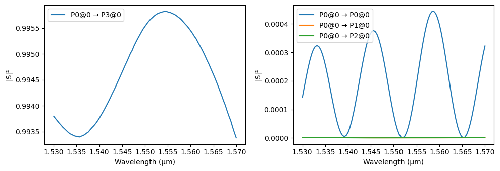
When routing complex circuits, waveguides inevitably need to cross. A standard intersection causes significant scattering loss and crosstalk. This component defines an adiabatic crossing, which gently expands the waveguide width using a cubic spline interpolation before the intersection, minimizing mode mismatch and radiation [2].
[8]:
default_widths = (
    0.5,
    0.6,
    0.95,
    1.32,
    1.44,
    1.46,
    1.466,
    1.52,
    1.58,
    1.62,
    1.76,
    2.15,
    0.5,
)


@pf.parametric_component(name_prefix="Angled Crossing")
def angled_adiabatic_crossing(
    *,
    port_spec="TE_1550_450",
    arm_length: pft.Dimension = 4.7,
    widths=(0.5, 0.6, 0.95, 1.32, 1.44, 1.46, 1.466, 1.52, 1.58, 1.62, 1.76, 2.15, 0.5),
    radius: pft.Dimension = bend_radius,
):
    """
    Create a 4-arm adiabatic crossing with smooth cubic taper profiles.

    Parameters:
        port_spec (str or PortSpec): Input/output port specification name or object.
        arm_length (float): Length of the main arm (µm).
        widths (Sequence[float]): Target waveguide widths (µm) along each arm.
        radius (float): Radius of the 45-deg arcs (µm).

    Returns:
        A crossing component.
    """
    if isinstance(port_spec, str):
        port_spec = pf.config.default_technology.ports[port_spec]

    wg_width, _ = port_spec.path_profile_for("Si")  # extract initial waveguide width

    # Number of points used to discretize the cubic spline profile.
    num_points = int(arm_length / pf.config.tolerance)

    # Calculate port locations based on input dimensions (projected to the 45° axes)
    projected_arm_length = arm_length * 2**-0.5
    arc_y = radius * 2**-0.5
    arc_x = radius - arc_y
    # Snap port coordinates to the grid to avoid gaps/overlaps
    xp = pf.snap_to_grid(projected_arm_length + arc_x)
    yp = pf.snap_to_grid(projected_arm_length + arc_y)

    # Create cubic spline interpolation for widths
    coords = np.linspace(0, projected_arm_length, len(widths))
    # Reverse widths, because we're starting from 0 at the center of the cross
    spline = make_interp_spline(coords, widths[::-1], k=3)

    # Pre-compute widths and positions from the interpolation
    coords = np.linspace(projected_arm_length, 0, num_points)
    widths = spline(coords)

    arm1 = pf.Path((xp, yp), wg_width)
    arm1.arc(
        0,
        -45,
        radius,
        width=(widths[0], "smooth"),
        endpoint=(projected_arm_length, projected_arm_length),
    )
    for x, w in zip(coords[1:], widths[1:]):
        arm1.segment((x, x), w)

    arm2 = arm1.copy().mirror()
    arm3 = arm1.copy().rotate(180)
    arm4 = arm2.copy().rotate(180)

    c = pf.Component("Angled Crossign")
    c.add("Si", *pf.boolean([arm1, arm2], [arm3, arm4], "+"))

    # Add ports
    c.add_port(c.detect_ports([port_spec]))
    assert len(c.ports) == 4, "Port detection failed: expected exactly 4 ports."

    # Add Tidy3D simulation model with symmetry conditions
    c.add_model(
        pf.Tidy3DModel(
            grid_spec=20,
            port_symmetries=[
                ("P1", "P0", "P3", "P2"),  # symmetry about x-axis
                ("P2", "P3", "P0", "P1"),  # symmetry about y-axis
                ("P3", "P2", "P1", "P0"),  # inversion symmetry
            ],
        ),
        "Tidy3DModel",
    )
    return c


angled_crossing = angled_adiabatic_crossing()
viewer(angled_crossing)
[8]:

[9]:
# Compute the scattering matrix of the crossing over the frequency range
s_matrix_angled_crossing = angled_crossing.s_matrix(freqs)

# Plot the magnitude of the S-matrix to evaluate transmission and crosstalk
_ = pf.plot_s_matrix(s_matrix_angled_crossing, input_ports=["P0"])
Uploading task 'P0@0…'
Starting task 'P0@0': https://tidy3d.simulation.cloud/workbench?taskId=fdve-86e8e7b3-b8f7-44c6-99df-00e8fd2a5367
Downloading data from 'P0@0'…
Progress: 100%
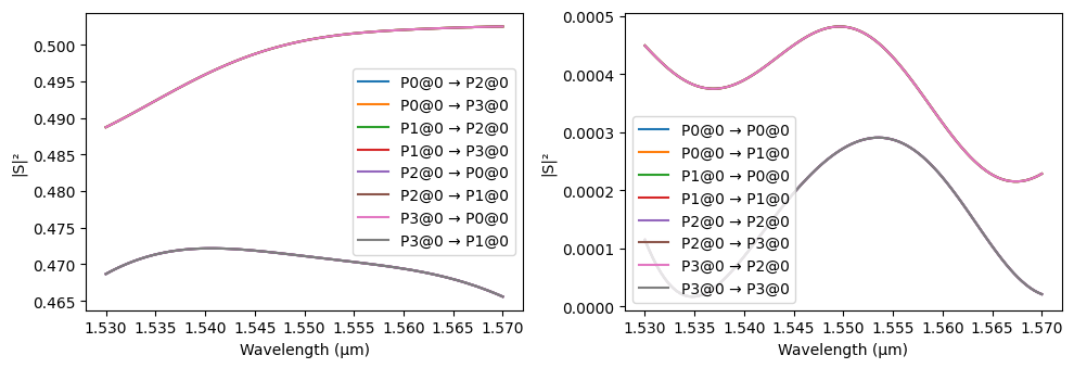
2x2 Multi-Mode Interferometer (MMI)
A 2x2 Multi-Mode Interferometer (MMI) is a robust and broadband component used to split or combine light based on the principle of self-imaging. We use the design presented in [3].
In this design, S-bends are used to smoothly transition light into the multimode region. Crucially, these bends create sufficient physical separation between the waveguides to allow for proper optical port placement. Without this separation, waveguide segments could overlap with adjacent port calculation boundaries, causing artificial errors during mode solving.
Because complex internal interference cannot be modeled analytically, a full-wave 3D FDTD model (Tidy3DModel) is attached, leveraging structural symmetries to significantly reduce simulation time.
[10]:
@pf.parametric_component(name_prefix="MMI2x2")
def mmi_2x2(
    *,
    port_spec="TE_1550_450",
    l1: pft.Dimension = 1.0,      # Length of the input taper sections
    l2: pft.Dimension = 2.4,      # Length of the main multimode interference body
    l3: pft.Dimension = 1.6,      # Length of the output taper sections
    w1: pft.Dimension = 1.48,     # Width parameters for the multimode body
    w2: pft.Dimension = 1.48,
    w4: pft.Dimension = 0.50,     # S-bend starting width
    w5: pft.Dimension = 0.70,     # Taper transition width
    w6: pft.Dimension = 0.20,     # Gap between the two input/output arms
    sbend_length: pft.Dimension = 2.0,
    sbend_offset: pft.Dimension = 0.2,
):
    if isinstance(port_spec, str):
        port_spec = pf.config.default_technology.ports[port_spec]

    mmi = pf.Component()

    # Extract the base waveguide width from the port specification
    wg_width, _ = port_spec.path_profile_for("Si")

    # Calculate the total width of the input/output interface region
    w3 = 2 * w5 + w6

    # Construct the upper input arm: an S-bend transitioning into a linear taper
    input_up = (
        pf.Path((-sbend_length, (w5 + w6) / 2 + sbend_offset), wg_width)
        .s_bend(endpoint=(0, (w5 + w6) / 2), width=w4)
        .segment((l1, 0), w5, relative=True)
    )

    # Mirror the upper input to create the lower input arm
    input_dn = input_up.copy().mirror()

    # Mirror the inputs across the center of the MMI body to create the output arms
    output_up = input_up.copy().mirror(
        axis_endpoint=(l1 + l2 + l3, 1),
        axis_origin=(l1 + l2 + l3, 0),
    )
    output_dn = output_up.copy().mirror()

    # Construct the central multimode interference body
    body = (
        pf.Path((l1, 0), w3)
        .segment((l2, 0), w1, relative=True)
        .segment((l3, 0), w2, relative=True)
        .segment((l3, 0), w2, relative=True)
        .segment((l2, 0), w3, relative=True)
    )

    # Add all physical geometries to the Silicon layer
    mmi.add("Si", input_up, input_dn, output_up, output_dn, body)

    # Detect and assign the four optical ports
    mmi.add_port(mmi.detect_ports([port_spec]))

    if len(mmi.ports) != 4:
        raise RuntimeError("MMI port detection failed: expected exactly 4 ports.")

    # Attach a full-wave 3D FDTD model for simulation
    # Symmetry definitions drastically reduce the required computational volume
    mmi.add_model(
        pf.Tidy3DModel(
            port_symmetries=[
                ("P1", "P0", "P3", "P2"), # Symmetry across the X-axis
                ("P2", "P3", "P0", "P1"), # Symmetry across the Y-axis
                ("P3", "P2", "P1", "P0"), # Inversion symmetry
            ],
        ),
        "Tidy3D",
    )

    return mmi

# Instantiate and view the 2x2 MMI
mmi = mmi_2x2()
viewer(mmi)
[10]:

[11]:
# Calculate the S-matrix over the specified wavelength range
s_matrix_mmi = mmi.s_matrix(freqs)

# Plot the calculated S-matrix
_ = pf.plot_s_matrix(s_matrix_mmi)
Uploading task 'P0@0…'
Starting task 'P0@0': https://tidy3d.simulation.cloud/workbench?taskId=fdve-5a03dd37-e703-4528-9320-b328d9301495
Downloading data from 'P0@0'…
Progress: 100%
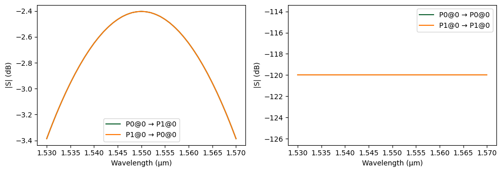
Grating Coupler
To interface our sub-micron photonic chip with macroscopic test equipment, we need to couple light in and out using standard single-mode optical fibers. This component defines a focusing grating coupler, which diffracts out-of-plane light coming from a tilted fiber directly into the fundamental mode of the planar silicon waveguide.
The physical layout utilizes a partially etched structure (Si slab) to optimize directionality and coupling efficiency. The specific geometric design of this focusing grating is based on the PhotonForge Grating Coupler example.
Rather than running a computationally expensive 3D FDTD simulation for this standard I/O structure, we attach an analytic DataModel. This model generates a scattering matrix based on a Gaussian transmission profile. The peak efficiency and bandwidth parameters used in this model are chosen to mimic the empirically measured results from the main reference of this tutorial [1].
[12]:
@pf.parametric_component(name_prefix="Grating Coupler")
def grating_coupler(
    *,
    port_spec="TE_1550_450",
    focal_length: pft.Dimension = 12.5,
    length: pft.Dimension = 15.5,
    period: pft.Dimension = 0.63,
    fill_factor: float = 0.5,
    fiber_translation: pft.Dimension = 0.0,
    fiber_angle_deg: float = 10.0,      # Standard tilt angle to avoid back-reflection
    aperture_angle_deg: float = 45.0,   # Opening angle of the focused grating
    center_wavelength: float = 1.55,
    peak_efficiency: float = 0.575,     # Empirical peak transmission
    bandwidth_fwhm: float = 0.07,       # Full Width at Half Maximum (in µm)
):
    if isinstance(port_spec, str):
        port_spec = pf.config.default_technology.ports[port_spec]

    # Free-space and fiber parameters
    n_env = 1.0
    input_length = 1.0
    waist_radius = 6.0
    gaussian_port_height = 0.5

    # Calculate the unit vector for the tilted optical fiber
    sin_angle = np.sin(np.deg2rad(fiber_angle_deg))
    cos_angle = np.cos(np.deg2rad(fiber_angle_deg))
    input_vector = (-sin_angle, 0, -cos_angle)

    grating_coupler = pf.Component("Grating_450")

    # Extract the waveguide input width to attach the grating
    si_layer = tech.layers["Si"].layer
    input_width = sum(w for w, _, layer in port_spec.path_profiles if layer == si_layer)

    # Add the short input waveguide segment
    for layer, path in port_spec.get_paths((0, 0)):
        grating_coupler.add(layer, path.segment((input_length, 0)))

    # Generate the curved stencil for the focusing grating
    grating = pf.stencil.focused_grating(
        center_wavelength,
        period,
        n_env * sin_angle,
        focal_length=focal_length,
        length=length,
        angle=aperture_angle_deg,
        fill_factor=fill_factor,
        input_width=input_width,
    )

    # Shift the generated grating to align with the input waveguide
    for shape in grating:
        shape.translate((input_length, 0))

    # Add the fully etched grating trenches to the Silicon layer
    grating_coupler.add("Si", *grating)

    # Add an envelope shape for the partial etch region (shallow grating)
    grating_coupler.add("Si Slab", pf.envelope(grating[1:], period))

    # Define the standard in-plane waveguide port (P0)
    grating_coupler.add_port(pf.Port((0, 0), 0, port_spec), "P0")

    # Define the out-of-plane Gaussian port (P1) representing the optical fiber
    gaussian_port_center = (
        np.array((focal_length + 0.5 * length + fiber_translation, 0, 0))
        + input_vector / input_vector[2] * gaussian_port_height
    )

    grating_coupler.add_port(
        pf.GaussianPort(
            gaussian_port_center,
            input_vector,
            waist_radius,
            polarization_angle=90,
            field_tolerance=1e-2,
        ),
        "P1",
    )

    # --------------------------------------------------------
    # Analytic Data Model Setup
    # --------------------------------------------------------
    # Generate S-parameters using a Gaussian curve rather than simulating
    wavelengths = np.linspace(1.5, 1.6, 101)
    freqs = pf.C_0 / wavelengths

    # Calculate transmission power based on peak efficiency and FWHM
    transmission_power = peak_efficiency * np.exp(
        -4 * np.log(2) * (wavelengths - center_wavelength) ** 2 / bandwidth_fwhm**2
    )
    s_mag = np.sqrt(transmission_power)

    # Populate the 2x2 S-matrix (S21 and S12)
    s_array = np.zeros((len(freqs), 2, 2), dtype=complex)
    s_array[:, 1, 0] = s_mag
    s_array[:, 0, 1] = s_mag

    # Attach the custom data model to the component
    grating_coupler.add_model(
        pf.DataModel(s_array=s_array, frequencies=freqs),
        "Gaussian Model",
    )

    return grating_coupler

# Instantiate and view the grating coupler
gc = grating_coupler()
viewer(gc)
[12]:

[13]:
# Calculate the S-matrix over the specified wavelength range
s_matrix_gc = gc.s_matrix(freqs)

# Plot the calculated S-matrix
_ = pf.plot_s_matrix(s_matrix_gc, y='dB')
Progress: 100%
Tunable Mach-Zehnder Interferometer (MZI)
A Tunable Mach-Zehnder Interferometer (MZI) is a fundamental building block for dynamically switching and routing light. It splits an input signal into two arms, applies a controlled phase shift to one arm using our previously defined thermo-optic phase shifter, and recombines the light. Depending on the applied heat, the resulting interference dictates which output port the light exits from.
[14]:
@pf.parametric_component(name_prefix="Tunable MZI")
def create_mzi(
    *,
    port_spec="TE_1550_450",
    heater_length: pft.Dimension = 100.0,
    propagation_loss: float = 3.0e-4,
    reference_frequency: float = freq0,
    dn_dT: float = 1.8e-4,
    heater_temp: float = 293.0,
    heater_width: pft.Dimension = 5.0,
    pad_width: pft.Dimension = 25.0,
    heater_overlap: pft.Dimension = 5.0,
):
    if isinstance(port_spec, str):
        port_spec = pf.config.default_technology.ports[port_spec]

    # Solve the strip waveguide mode at the carrier frequency for routing bends
    mode_solver = pf.port_modes(
        port_spec,
        [reference_frequency],
        mesh_refinement=50,
        group_index=True,
        show_progress=False,
    )
    n_eff = mode_solver.data.n_eff.isel(mode_index=0).item()
    n_group = mode_solver.data.n_group.isel(mode_index=0).item()

    # 1. Instantiate the sub-components for the MZI arms
    wg = create_wg(
        port_spec=port_spec,
        length=heater_length,
        propagation_loss=propagation_loss,
        reference_frequency=reference_frequency,
    )

    tps = thermo_optic_phase_shifter(
        port_spec=port_spec,
        heater_length=heater_length,
        heater_width=heater_width,
        pad_width=pad_width,
        heater_overlap=heater_overlap,
        propagation_loss=propagation_loss,
        reference_frequency=reference_frequency,
        dn_dT=dn_dT,
        temperature=heater_temp,
    )

    # 2. Define routing S-bends with analytic models to connect the MMIs to the arms
    s_bend_model = pf.AnalyticWaveguideModel(
        n_eff=n_eff,
        reference_frequency=freq0,
        propagation_loss=propagation_loss,
        n_group=n_group,
    )
    s_bend_up = pf.parametric.s_bend(
        port_spec=port_spec, length=bend_radius, offset=bend_radius, model=s_bend_model
    )
    s_bend_down = pf.parametric.s_bend(
        port_spec=port_spec, length=bend_radius, offset=-bend_radius, model=s_bend_model
    )

    # Instantiate the 2x2 MMI for splitting and recombining
    mmi = mmi_2x2(port_spec=port_spec)

    # 3. Define the netlist to logically connect the components together
    netlist_mzi = {
        "name": "Tunable MZI",
        "instances": {
            "mmi_in": mmi,          # Input splitter
            "mmi_out": mmi,         # Output combiner
            "tps": tps,             # Active tuning arm
            "wg": wg,               # Passive reference arm
            "sb0": s_bend_down,     # Routing bends
            "sb1": s_bend_up,
            "sb2": s_bend_up,
            "sb3": s_bend_down,
        },
        # Map out the port-to-port connections
        "connections": [
            (("sb0", "P0"), ("mmi_in", "P2")),
            (("wg", "P0"), ("sb0", "P1")),
            (("sb1", "P0"), ("mmi_in", "P3")),
            (("tps", "P0"), ("sb1", "P1")),
            (("sb2", "P0"), ("wg", "P1")),
            (("sb3", "P0"), ("tps", "P1")),
            (("mmi_out", "P1"), ("sb3", "P1")),
        ],
        # Expose the outer ports of the MMIs as the external ports of the MZI
        "ports": [
            ("mmi_in", "P0"),
            ("mmi_in", "P1"),
            ("mmi_out", "P2"),
            ("mmi_out", "P3"),
        ],
        # Terminals will be used for electrical routing
        "terminals": [
            ("tps", "T0"),
            ("tps", "T1"),
        ],
        # Circuit model assigned
        "models": [(pf.CircuitModel(), "Circuit")],
    }

    # Generate the physical layout from the netlist
    return pf.component_from_netlist(netlist_mzi)

# Instantiate and view the Tunable MZI
mzi = create_mzi()
viewer(mzi)
[14]:

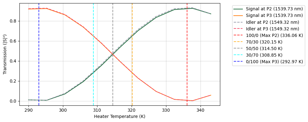
MZI Thermal Sweep and State Calibration
To effectively use the Tunable MZI as a routing component, we must map its physical heater temperature to its optical splitting behavior. This cell processes the S-matrix over a temperature sweep to find the exact operational points for various splitting ratios.
Using cubic spline interpolation, we extract the precise transmission values at our target quantum wavelengths (1539.73 nm and 1549.32 nm). We then calculate the fractional power routed to the “bar” port (P2) versus the “cross” port (P3). By fitting this ratio to a continuous curve, we can accurately extract the specific temperatures required to configure the MZI as a perfect switch (100/0 or 0/100) or a variable beam splitter (e.g., 50/50).
[15]:
# 1. Define the temperature sweep range (in Kelvin)
temperatures = np.linspace(290, 343, 11)

# Arrays to store the calculated transmission powers
T_signal_P2 = []
T_idler_P3 = []
T_signal_P3 = []
T_idler_P2 = []

print("Starting temperature sweep with wavelength interpolation...")

for T in temperatures:
    # 2. Update the MZI with the new temperature
    mzi.update(heater_temp=T)

    # 3. Compute the S-matrix over the FULL frequency array
    s_matrix = mzi.s_matrix(freqs, show_progress=False)

    # 4. Extract the full S-parameter arrays
    s20_full = s_matrix[("P0@0", "P2@0")]
    s30_full = s_matrix[("P0@0", "P3@0")]

    # 5. Interpolate directly against the sorted wavelengths array
    interp_s20 = interp1d(wavelengths, s20_full, kind="cubic")
    interp_s30 = interp1d(wavelengths, s30_full, kind="cubic")

    # 6. Evaluate the interpolated functions at the specific target wavelengths
    s20_signal = interp_s20(signal_wavelength)
    s30_signal = interp_s30(signal_wavelength)
    s20_idler = interp_s20(idler_wavelength)
    s30_idler = interp_s30(idler_wavelength)

    # Calculate linear transmission (|S|^2)
    T_signal_P2.append(np.abs(s20_signal) ** 2)
    T_signal_P3.append(np.abs(s30_signal) ** 2)
    T_idler_P2.append(np.abs(s20_idler) ** 2)
    T_idler_P3.append(np.abs(s30_idler) ** 2)

# Convert to numpy arrays
T_signal_P2 = np.array(T_signal_P2)
T_signal_P3 = np.array(T_signal_P3)
T_idler_P2 = np.array(T_idler_P2)
T_idler_P3 = np.array(T_idler_P3)

from scipy.interpolate import UnivariateSpline

# Normalize the signal to find the fractional ratio going to P2
# This automatically handles any baseline insertion loss
ratio_P2 = T_signal_P2 / (T_signal_P2 + T_signal_P3)

# Fit a spline to this ratio
ratio_spline = UnivariateSpline(temperatures, ratio_P2, s=0, k=4)
ratio_derivative = ratio_spline.derivative()

# Define a helper function to find specific split temperatures
def get_split_temp(target_ratio):
    if target_ratio == 1.0:
        # 100/0 state: Find the local maximum (where derivative is 0)
        extrema = ratio_derivative.roots()
        return max(extrema, key=lambda t: ratio_spline(t)) if len(extrema) > 0 else None
    elif target_ratio == 0.0:
        # 0/100 state: Find the local minimum (where derivative is 0)
        extrema = ratio_derivative.roots()
        return min(extrema, key=lambda t: ratio_spline(t)) if len(extrema) > 0 else None
    else:
        # Fractional states: Shift the spline by the target ratio and find the root
        shifted_spline = UnivariateSpline(temperatures, ratio_P2 - target_ratio, s=0)
        roots = shifted_spline.roots()
        return roots[0] if len(roots) > 0 else None

# Define the splits we want to map and their plot colors
splits = {
    "100/0 (Max P2)": {"ratio": 1.0, "color": "red"},
    "70/30": {"ratio": 0.7, "color": "orange"},
    "50/50": {"ratio": 0.5, "color": "gray"},
    "30/70": {"ratio": 0.3, "color": "cyan"},
    "0/100 (Max P3)": {"ratio": 0.0, "color": "blue"}
}


# Plot the sweep results
plt.figure(figsize=(10,4))
plt.plot(temperatures, T_signal_P2, label="Signal at P2 (1539.73 nm)")
plt.plot(temperatures, T_signal_P3, label="Signal at P3 (1539.73 nm)")
plt.plot(temperatures, T_idler_P2, '--', label="Idler at P2 (1549.32 nm)")
plt.plot(temperatures, T_idler_P3, '--', label="Idler at P3 (1549.32 nm)")
plt.xlabel("Heater Temperature (K)")
plt.ylabel("Transmission (|S|²)")
plt.legend()
plt.grid(True, alpha=0.5)

print("--- Operating Temperatures ---")
for label, params in splits.items():
    t_val = get_split_temp(params["ratio"])

    if t_val is not None:
        print(f"{label:<15}: {t_val:.2f} K")
        # Plot the vertical line for each state
        plt.axvline(t_val, color=params["color"], linestyle='--', linewidth=1.5, alpha=0.8,
                    label=f'{label} ({t_val:.2f} K)')
    else:
        print(f"{label:<15}: Not found in sweep range")

plt.legend(bbox_to_anchor=(1.05, 1), loc='upper left')
plt.tight_layout()
plt.show()
Starting temperature sweep with wavelength interpolation...
07:25:58 -03 Loading simulation from local cache. View cached task using web UI
             at
             'https://tidy3d.simulation.cloud/workbench?taskId=fdve-5a03dd37-e70
             3-4528-9320-b328d9301495'.
--- Operating Temperatures ---
100/0 (Max P2) : 336.06 K
70/30          : 320.15 K
50/50          : 314.50 K
30/70          : 308.85 K
0/100 (Max P3) : 292.95 K
[16]:
# Extract specific operational temperatures for routing
T_BAR = get_split_temp(splits["100/0 (Max P2)"]["ratio"])
T_CROSS = get_split_temp(splits["0/100 (Max P3)"]["ratio"])

print(f"Stored T_BAR:   {T_BAR:.2f} K")
print(f"Stored T_CROSS: {T_CROSS:.2f} K")
Stored T_BAR:   336.06 K
Stored T_CROSS: 292.95 K
Asymmetric Mach-Zehnder Interferometer (AMZI) Filter Design
To separate the signal and idler photons, an AMZI relies on a deliberate path length difference between its two routing arms. This difference creates a frequency-dependent phase shift, causing constructive interference for one frequency at the “cross” port and for another frequency at the “bar” port.
1. Defining the Target Variables
\(c\): Speed of light in a vacuum
\(n_g\): Group index of the specific waveguide geometry
\(\nu_{FSR}\): The Free Spectral Range (in frequency)
2. Calculating the Path Length Difference
The core design parameter of an AMZI is the physical path length difference (\(\Delta L\)) required to achieve the desired FSR. This is dictated by the equation:
To separate two specific frequencies (\(\nu_{signal}\) and \(\nu_{idler}\)) to two different output ports, the frequency difference must correspond exactly to a half-FSR (\(\pi\) phase shift difference). Therefore, the target FSR for the device is:
3. Calculating the Bend Radius for a U-Shape Delay
For a “trombone” or “U-shape” delay line where both arms span the same horizontal distance, the top arm uses four 90-degree bends and a straight section, while the bottom arm is purely straight.
Top Arm Length: \(L_{top} = 2\pi R + L_{heater}\)
Bottom Arm Length: \(L_{bottom} = 4R + L_{heater}\)
The heater length cleanly cancels out when taking the difference (\(\Delta L = L_{top} - L_{bottom}\)), resulting in:
Rearranging to solve for the required bend radius (\(R\)):
[17]:
@pf.parametric_component(name_prefix="Asymmetric MZI")
def create_amzi(
    *,
    port_spec="TE_1550_450",
    heater_length: pft.Dimension = 100.0,
    propagation_loss: float = 3.0e-4,
    reference_frequency: float = freq0,
    signal_frequency: float = signal_frequency,
    idler_frequency: float = idler_frequency,
    dn_dT: float = 1.8e-4,
    heater_temp: float = 305.0,
    heater_width: pft.Dimension = 5.0,
    pad_width: pft.Dimension = 25.0,
    heater_overlap: pft.Dimension = 5.0,
):
    if isinstance(port_spec, str):
        port_spec = pf.config.default_technology.ports[port_spec]

    # Solve the strip waveguide mode at the carrier frequency
    mode_solver = pf.port_modes(
        port_spec,
        [reference_frequency],
        mesh_refinement=50,
        group_index=True,
        show_progress=False,
    )
    n_eff = mode_solver.data.n_eff.isel(mode_index=0).item()
    n_group = mode_solver.data.n_group.isel(mode_index=0).item()

    # Calculate required path length difference (Delta L) in meters
    fsr = 2 * np.abs(signal_frequency - idler_frequency)
    delta_L = pf.C_0 / (n_group * fsr)

    # Calculate the required bend radius (R)
    # Based on the geometry: Delta L = 2*pi*R - 4*R = 2*R*(pi - 2)
    bend_radius = pf.snap_to_grid(delta_L / (2 * (np.pi - 2)))

    wg = create_wg(
        port_spec=port_spec,
        length=heater_length + 4 * bend_radius,
        propagation_loss=propagation_loss,
        reference_frequency=reference_frequency,
    )

    tps = thermo_optic_phase_shifter(
        port_spec=port_spec,
        heater_length=heater_length,
        heater_width=heater_width,
        pad_width=pad_width,
        heater_overlap=heater_overlap,
        propagation_loss=propagation_loss,
        reference_frequency=reference_frequency,
        dn_dT=dn_dT,
        temperature=heater_temp,
    )

    bend = create_bend(
        port_spec=port_spec,
        reference_frequency=reference_frequency,
        radius=bend_radius,
        propagation_loss=propagation_loss,
    )

    mmi = mmi_2x2(port_spec=port_spec)

    # Define netlist for creating the Asymmetric MZI
    netlist_amzi = {
        "name": "Asymmetric MZI",
        "instances": {
            "mmi_in": mmi,
            "mmi_out": mmi,
            "tps": tps,
            "wg": wg,
            "b0": bend,
            "b1": bend,
            "b2": bend,
            "b3": bend,
        },
        "connections": [
            (("wg", "P0"), ("mmi_in", "P2")),
            (("b0", "P0"), ("mmi_in", "P3")),
            (("b1", "P1"), ("b0", "P1")),
            (("tps", "P0"), ("b1", "P0")),
            (("b2", "P1"), ("tps", "P1")),
            (("b3", "P0"), ("b2", "P0")),
            (("mmi_out", "P1"), ("b3", "P1")),
        ],
        # External ports definition for further connectivity
        "ports": [
            ("mmi_in", "P0"),
            ("mmi_in", "P1"),
            ("mmi_out", "P2"),
            ("mmi_out", "P3"),
        ],
        # Terminals will be used for electrical routing
        "terminals": [
            ("tps", "T0"),
            ("tps", "T1"),
        ],
        # Circuit model assigned to the unit cell
        "models": [(pf.CircuitModel(), "Circuit")],
    }

    # Create the component from the defined netlist
    amzi = pf.component_from_netlist(netlist_amzi)

    return amzi


amzi = create_amzi()
viewer(amzi)
[17]:

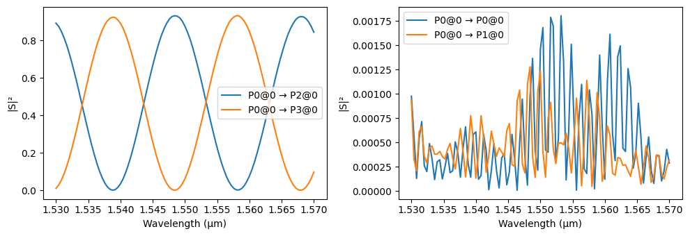
[18]:
# Calculate the S-matrix over the specified wavelength range
s_matrix_amzi = amzi.s_matrix(freqs)

# Plot the calculated S-matrix
_ = pf.plot_s_matrix(s_matrix_amzi, input_ports=["P0"])
Uploading task 'Mode-StripTE1550nmw450nm…'
Uploading task 'Mode-StripTE1550nmw450nm…'
Uploading task 'Mode-StripTE1550nmw450nm…'
Uploading task 'Mode-StripTE1550nmw450nm…'
Starting task 'Mode-StripTE1550nmw450nm': https://tidy3d.simulation.cloud/workbench?taskId=mo-2c9a6edf-58ec-488f-b1de-2913b7e34189
Starting task 'Mode-StripTE1550nmw450nm': https://tidy3d.simulation.cloud/workbench?taskId=mo-8e3bf04a-eb79-4558-9436-c038da5d8b8f
Starting task 'Mode-StripTE1550nmw450nm': https://tidy3d.simulation.cloud/workbench?taskId=mo-dbb65bdd-63af-4352-a179-4f30a0224d60
Starting task 'Mode-StripTE1550nmw450nm': https://tidy3d.simulation.cloud/workbench?taskId=mo-5c63cd6a-93cf-46a1-92f4-00053bb11b4a
Downloading data from 'Mode-StripTE1550nmw450nm'…
Downloading data from 'Mode-StripTE1550nmw450nm'…
Downloading data from 'Mode-StripTE1550nmw450nm'…
Downloading data from 'Mode-StripTE1550nmw450nm'…
Progress: 100%
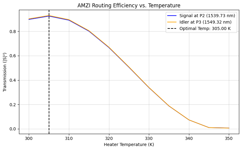
AMZI Thermal Optimization
This cell executes a temperature sweep from 300 K to 350 K to optimize the routing of signal and idler photons to ports P2 and P3, respectively. By iteratively updating the AMZI’s heater temperature and computing the S-matrix, the script employs cubic spline interpolation via scipy.interpolate.interp1d to accurately determine transmission at the exact target wavelengths (\(1.53973\) μm and \(1.54932\) μm) within the simulated grid. The optimal operating point is
identified by maximizing a “fitness” product of both transmission values (\(T_{signal} \times T_{idler}\)), ensuring high-extinction routing for both channels simultaneously as visualized in the resulting sweep plot.
[19]:
from scipy.interpolate import interp1d

# 1. Define the temperature sweep range (in Kelvin)
temperatures = np.linspace(300, 360, 15)

# Arrays to store the calculated transmission powers
T_signal_P2 = []
T_idler_P3 = []

print("Starting temperature sweep with wavelength interpolation...")

for T in temperatures:
    # 2. Update the AMZI with the new temperature
    amzi.update(heater_temp=T)

    # 3. Compute the S-matrix over the FULL frequency array
    s_matrix = amzi.s_matrix(freqs, show_progress=False)

    # 4. Extract the full S-parameter arrays
    s20_full = s_matrix[("P0@0", "P2@0")]
    s30_full = s_matrix[("P0@0", "P3@0")]

    # 5. Interpolate directly against the sorted wavelengths array
    interp_s20 = interp1d(wavelengths, s20_full, kind="cubic")
    interp_s30 = interp1d(wavelengths, s30_full, kind="cubic")

    # 6. Evaluate the interpolated functions at the specific target wavelengths
    s20_signal = interp_s20(signal_wavelength)
    s30_idler = interp_s30(idler_wavelength)

    # Calculate linear transmission (|S|^2)
    T_signal_P2.append(np.abs(s20_signal) ** 2)
    T_idler_P3.append(np.abs(s30_idler) ** 2)

# Convert to numpy arrays
T_signal_P2 = np.array(T_signal_P2)
T_idler_P3 = np.array(T_idler_P3)

# 7. Find the optimal temperature
fitness = T_signal_P2 * T_idler_P3
optimal_idx = np.argmax(fitness)
optimal_temp = temperatures[optimal_idx]

print("-" * 30)
print(f"Optimal Heater Temperature: {optimal_temp:.2f} K")
print(f"Signal Transmission (P0 -> P2): {T_signal_P2[optimal_idx]:.4f}")
print(f"Idler Transmission  (P0 -> P3): {T_idler_P3[optimal_idx]:.4f}")
print("-" * 30)

# 8. Plot the sweep results
plt.figure(figsize=(8, 5))
plt.plot(temperatures, T_signal_P2, label="Signal at P2 (1539.73 nm)", color="blue")
plt.plot(temperatures, T_idler_P3, label="Idler at P3 (1549.32 nm)", color="orange")
plt.axvline(
    optimal_temp,
    color="black",
    linestyle="--",
    label=f"Optimal Temp: {optimal_temp:.2f} K",
)

plt.xlabel("Heater Temperature (K)")
plt.ylabel("Transmission (|S|²)")
plt.title("AMZI Routing Efficiency vs. Temperature")
plt.legend()
plt.grid(True, alpha=0.5)
plt.tight_layout()
plt.show()
Starting temperature sweep with wavelength interpolation...
------------------------------
Optimal Heater Temperature: 351.43 K
Signal Transmission (P0 -> P2): 0.9232
Idler Transmission  (P0 -> P3): 0.9293
------------------------------
Photon-Pair Source (SFWM Spiral)
This component serves as the heart of the quantum circuit: the photon-pair generation source. We utilize a long spiral waveguide to generate correlated signal and idler photons via Spontaneous Four-Wave Mixing (SFWM).
Because SFWM is a relatively weak non-linear optical process in silicon, a long interaction length is required to achieve a sufficient generation rate. Here, we generate a tightly coiled circular spiral with a total optical path length of 15,000 µm (15 mm) to maximize this non-linear interaction while maintaining a compact physical footprint on the chip [1].
[20]:
spiral = pf.parametric.circular_spiral(full_length=15_000)
viewer(spiral)
[20]:

Bond Pads
Bond pads are the primary electrical interface between the photonic chip and the external environment. These large metal areas (typically 100 × 100 µm) are designed for wire bonding or flip-chip packaging, providing reliable electrical connections for DC biasing of heaters and high-speed RF signaling for modulators. The design ensures low contact resistance and sufficient surface area to accommodate standard packaging tolerances.
[21]:
bp = pf.Component("BondPad")
bp.add_terminal(pf.Terminal("M2_router", pf.Rectangle(size=(100, 100))), add_structure=True)
bp.add("M_Open", pf.Rectangle(size=(95, 95)))
viewer(bp)
[21]:
