Getting Started
If you don’t have PhotonForge already installed, please follow the installation instructions first.
If you prefer video tutorials for both web GUI and Python, you’ll find the in our learning center.
In this section you’ll learn more about the key concepts in PhotonForge and how to get started with your first design. We start by quickly presenting those concepts:
Component

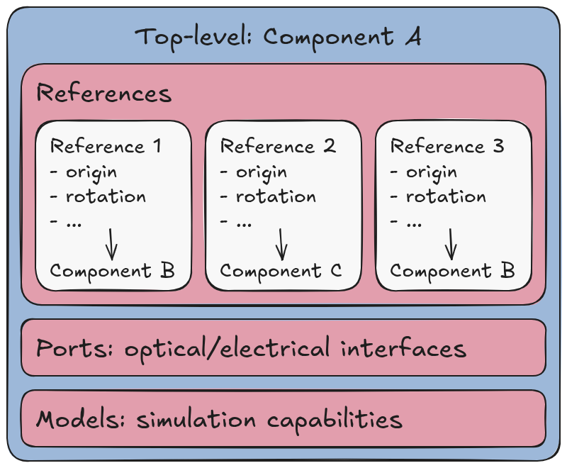
All devices within PhotoForge are represented by a Component.
Components contain all the geometrical and logical structures that are used to model and simulate the physical device.
Most fabrication processes require devices to be described by a 2D layout, usually stored as a GDSII or OASIS file.
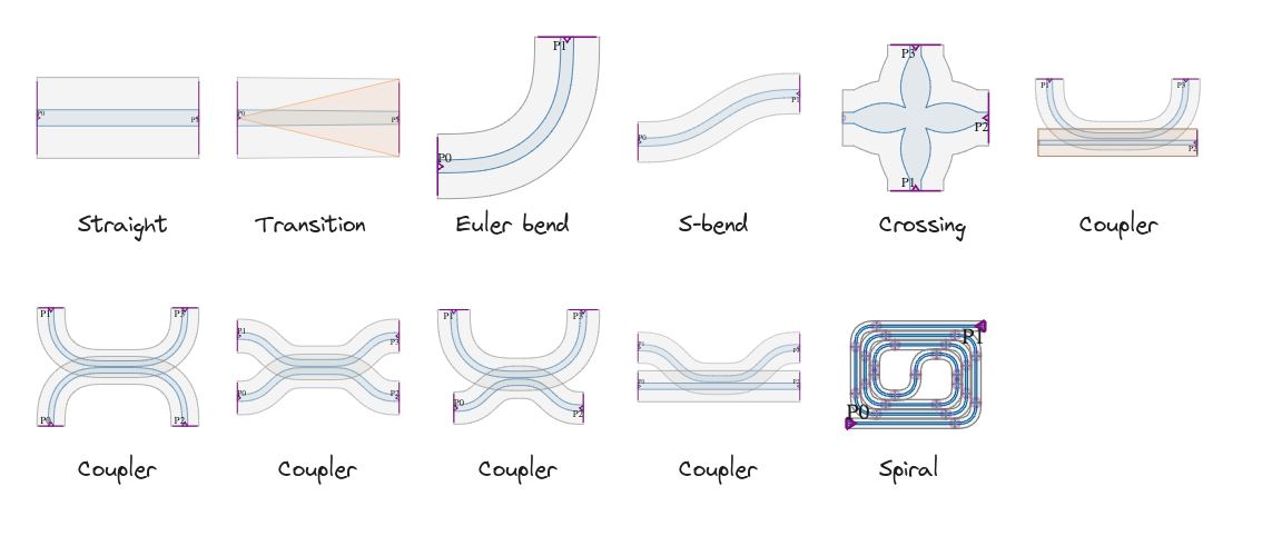
PhotonForge components can also be described by 2D geometries to transparently integrate with layout files.
Components can also be hierarchically nested through Reference instances, which allows the re-use of sub-components to build larger and more complex systems.

Technology

Full electromagnetic simulation of those components requires a 3D representation of the device.
Traditionally, the missing information required to render and accurately simulate the device in 3D from a 2D layout is derived from the intended fabrication process, through a PDK (process design kit).
In PhotonForge, the PDK information is stored in a Technology object, which can be created and customized by the user, or directly provided by the foundry that will execute the fabrication.
Ports

A component must somehow connect to other components or the external world.
That connection is created by adding Port objects to a component, which simply represents the terminating cross-section of a waveguide.
The set of ports of a component defines the shape of its scattering parameters (S parameters) response, which is used throughout PhotonForge to characterize the device.
Models

Finally, to bridge the layout description of the device to its S parameters, models are added to the component to perform that computation according to the component’s internal structures and ports. Models can be as simple as an ideal analytical model, or as complete as a Tidy3D FDTD simulation of the 3D component geometry, or anything in between, including circuit-type simulations that chain together the models from a component’s sub-components.
First Run
 1import numpy as np
 2import photonforge as pf
 3
 4# Set the default project technology
 5tech = pf.basic_technology()
 6pf.config.default_technology = tech
 7
 8# Create an S bend from the parametric component library using the "Strip" waveguide profile defined
 9# in the Basic Technology
10s_bend = pf.parametric.s_bend(port_spec="Strip", length=4, offset=1.5, model=pf.Tidy3DModel())
11
12# Get the S parameters (uses the default Tidy3D Model)
13wavelengths = np.linspace(1.5, 1.6, 11)
14freqs = pf.C_0 / wavelengths
15s_matrix = s_bend.s_matrix(freqs)
16
17# We can easily plot the S parameters with the following utility
18fig, ax = pf.plot_s_matrix(s_matrix)
The parametric.s_bend() function creates a parametric component with 2 ports and a default Tidy3DModel model.
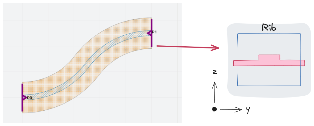
If we look at the created s_bend component in a Jupyter notebook, we can see an SVG representation of the geometry and ports, as below.
Parametric S bend for a “Strip” waveguide.
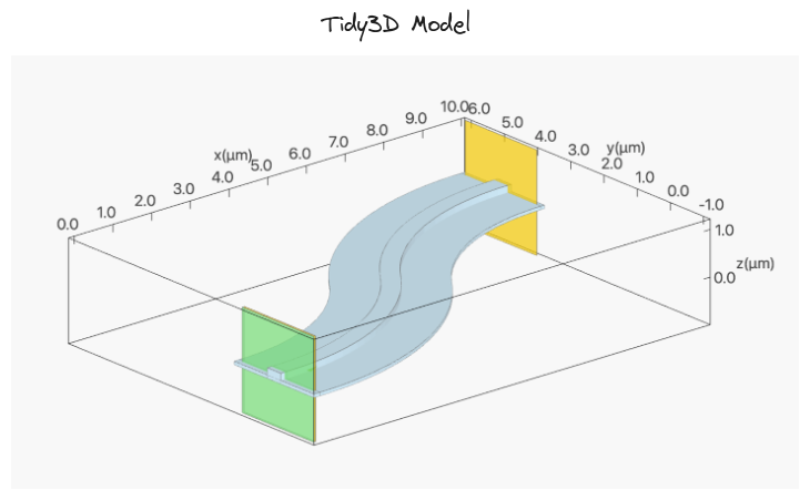
When we calculate the S parameters in line 15, the model generates a Tidy3D simulation that is automatically run and provides the required scattering coefficients.
Line 18 uses the plot_s_matrix() utility function to quickly plot the S parameters:
S parameters for the parametric S bend.
Note
The S parameters are cached by Tidy3DModel, so the FDTD simulation can be skipped in future runs as long as there are no changes to it.
From here, we can look into full Examples to see the full capabilities of PhotonForge, dive deeper into specific topics in the Short Guides section, or explore the Python API Reference for the full module documentation.