
Foundry-Compatible PIC Design Flow

In this demo, we’ll learn how to:
Load PDK components and custom components from GDSII files;
Run component-level simulations (MODE, FDTD);
Create a netlist-driven layout of components; and
Simulate the complete photonics circuit.
We begin by loading PhotonForge, Tidy3D, the SiEPIC OpenEBL PDK, and other common Python modules we will be using.
[1]:
import matplotlib.pyplot as plt
import numpy as np
import photonforge as pf
import siepic_forge as siepic
import tidy3d as td

# Start the live viewer for interactive visualization
from photonforge.live_viewer import LiveViewer

viewer = LiveViewer()
07:28:29 -03 WARNING: The material-library variant 'Palik_Lossless' is
             deprecated and maps to 'Palik_LowLoss' because it contains a tiny
             fitted loss despite its name. Use 'Palik_NoLoss' where available
             for a zero-loss Palik model.
LiveViewer started at http://localhost:39139
We use the default SiEPIC PDK as our default technology and set some configurations.
[2]:
tech = siepic.ebeam()
pf.config.default_technology = tech

# We lower the default mesh refinement to decrease the sizes of the simulations.
# For more accurate results, higher values should be used.
pf.config.default_mesh_refinement = 12

pf.config.svg_labels = False
td.config.logging.level = "ERROR"

# Set frequency range
wavelengths = np.linspace(1.5, 1.6, 101)
Review the available layers in the PDK:
[3]:
tech.layers
[3]:
| Name | Layer | Description | Color | Pattern |
|---|---|---|---|---|
| Si | (1, 0) | SiEPIC - Waveguide | #ff80a818 | \\ |
| PinRec | (1, 10) | SiEPIC | #ff80a818 | xx |
| PinRecM | (1, 11) | SiEPIC | #80000018 | + |
| Si Slab | (2, 0) | Dedicated Run Layers - Device…… Layer Partial Etch | #c080ff18 | / |
| Direct Metal | (5, 0) | Dedicated Run Layers | #80a8ff18 | || |
| Oxide open to BOX | (6, 0) | Dedicated Run Layers | #ff000018 | - |
| Text | (10, 0) | Text-Not Fabricated | #00000018 | hollow |
| M1_heater | (11, 0) | TiW Heater | #0000ff18 | \\ |
| M2_router | (12, 0) | TiW/Au Routing Bilayer | #ffbf0018 | // |
| M_Open | (13, 0) | Bond Pad Open | #80005718 | \\ |
| Si n | (20, 0) | Dedicated Run Layers | #afff8018 | - |
| Si p | (21, 0) | Dedicated Run Layers | #ffd9df18 | = |
| Si n+ | (22, 0) | Dedicated Run Layers | #ff800018 | x |
| Si p+ | (23, 0) | Dedicated Run Layers | #ddff0018 | xx |
| Si n++ | (24, 0) | Dedicated Run Layers | #00ffff18 | + |
| Si p++ | (25, 0) | Dedicated Run Layers | #00800018 | ++ |
| ANT Reserved | (31, 0) | SiEPIC/ANT Reserved | #9580ff18 | / |
| ANT Reserved 1 | (33, 0) | ANT Reserved | #9580ff18 | / |
| Via to silicon | (40, 0) | Dedicated Run Layers | #0000ff18 | . |
| DevRec | (68, 0) | SiEPIC | #00800018 | . |
| FbrTgt | (81, 0) | SiEPIC/Dedicated Run Layers | #80808018 | ++ |
| ANT Reserved 2 | (102, 0) | ANT Reserved | #9580ff18 | / |
| ANT Reserved 3 | (110, 0) | ANT Reserved | #9580ff18 | / |
| Custom Dicing | (189, 0) | #00000018 | hollow | |
| SEM Imaging | (200, 0) | #ff000018 | x | |
| Deep Trench | (201, 0) | #00ff0018 | . | |
| Deep Trench Handling Exclusion | (202, 0) | #00760018 | : | |
| Thermal Isolation Trenches | (203, 0) | #00800018 | \ | |
| Laser Integration Shelf | (205, 0) | Dedicated Run Layers | #69ff0518 | xx |
| Floor Plan-Not Fabricated | (290, 0) | #c080ff18 | hollow | |
Error: device layer width is…… less than design rule | (301, 0) | DRC Errors | #80005718 | = |
Error: device layer spacing is…… less than design rule | (301, 1) | DRC Errors | #80005718 | - |
Warning: polygons/paths on…… PinRec layer (1/10) will NOT be fabricated | (301, 2) | DRC Errors | #80005718 | || |
Error: direct metal width is…… less than 5 microns | (305, 0) | DRC Errors | #80808018 | ++ |
Error: direct metal spacing is…… less than 10 microns | (305, 1) | DRC Errors | #80808018 | + |
Error: TiW width is less than 3…… microns | (311, 0) | DRC Errors | #ffa08018 | // |
Error: TiW spacing is less than…… 3 microns | (311, 1) | DRC Errors | #ffa08018 | / |
Error: Al width is less than…… design rule | (312, 0) | DRC Errors | #00ffff18 | | |
Error: Al spacing is less than…… design rule | (312, 1) | DRC Errors | #00ffff18 | // |
Error: Spacing between TiW and…… Al is less than 5 microns | (312, 3) | DRC Errors | #00ffff18 | \\ |
Error: Oxide window width is…… less than 10 microns | (313, 0) | DRC Errors | #01ff6b18 | || |
Error: Oxide window spacing is…… less than 10 microns | (313, 1) | DRC Errors | #01ff6b18 | | |
Error: Oxide window is not…… placed over Al | (313, 2) | DRC Errors | #01ff6b18 | // |
| Standard Design Area | (350, 0) | DRC Errors | #ddff0018 | \ |
Error: Features outside design…… area. Verify design size and centering. | (350, 1) | DRC Errors | #ddff0018 | : |
Error: Dicing lane width is…… less than 100 microns | (389, 0) | DRC Errors | #ff00ff18 | ++ |
Error: Spacing between dicing…… lane and devices is less than 50 microns | (389, 1) | DRC Errors | #ff00ff18 | + |
Error: SEM width is less than…… 500 nm | (400, 0) | DRC Errors | #ff9d9d18 | x |
| Deep Trench Design Area | (401, 0) | DRC Errors | #80a8ff18 | xx |
Error: Metal, SEM, or handling…… region overlap with deep trenches. Verify design centering | (401, 1) | DRC Errors | #80a8ff18 | x |
Warning: Silicon features…… outside deep trench design area. Verify accuracy before submission | (401, 2) | DRC Errors | #80a8ff18 | = |
Error: Spacing between metal…… and deep trench is less than 30 microns | (401, 3) | DRC Errors | #80a8ff18 | - |
Error: Deep trench width is…… less than 260 microns | (401, 4) | DRC Errors | #80a8ff18 | || |
Error: Deep trench handling…… area missing. Please add handling area of size shown by polygons | (402, 0) | DRC Errors | #ff000018 | + |
Error: Features inside deep…… trench handling area | (402, 1) | DRC Errors | #ff000018 | xx |
Error: Thermal isolation width…… is less than design rule | (403, 0) | DRC Errors | #50008018 | ++ |
Error: Thermal isolation…… spacing is less than design rule | (403, 1) | DRC Errors | #50008018 | + |
Error: Spacing between thermal…… isolation and metal is less than design rule | (403, 2) | DRC Errors | #50008018 | xx |
Error: Thermal isolation and…… device layer overlap, or spacing is less than design rule | (403, 3) | DRC Errors | #50008018 | x |
Dream Photonics Black Box-Not…… Fabricated | (998, 0) | #00000018 | hollow | |
| Errors | (999, 0) | SiEPIC | #0000ff18 | || |
Inspect available PDK components:
[4]:
siepic.component_names
[4]:
{'GC_TE_1310_8degOxide_BB',
 'GC_TE_1550_8degOxide_BB',
 'GC_TM_1310_8degOxide_BB',
 'GC_TM_1550_8degOxide_BB',
 'ebeam_adiabatic_te1550',
 'ebeam_adiabatic_tm1550',
 'ebeam_bdc_te1550',
 'ebeam_crossing4',
 'ebeam_gc_te1550',
 'ebeam_gc_tm1550',
 'ebeam_routing_taper_te1550_w=500nm_to_w=3000nm_L=20um',
 'ebeam_routing_taper_te1550_w=500nm_to_w=3000nm_L=40um',
 'ebeam_splitter_swg_assist_te1310',
 'ebeam_splitter_swg_assist_te1550',
 'ebeam_terminator_te1310',
 'ebeam_terminator_te1550',
 'ebeam_terminator_tm1550',
 'ebeam_y_1310',
 'ebeam_y_1550',
 'ebeam_y_adiabatic',
 'ebeam_y_adiabatic_500pin',
 'taper_si_simm_1310',
 'taper_si_simm_1550'}
Loading a PDK component
We will use a couple of components readily available in the PDK.
[5]:
gc = siepic.component("ebeam_gc_te1550")
viewer(gc)
[5]:

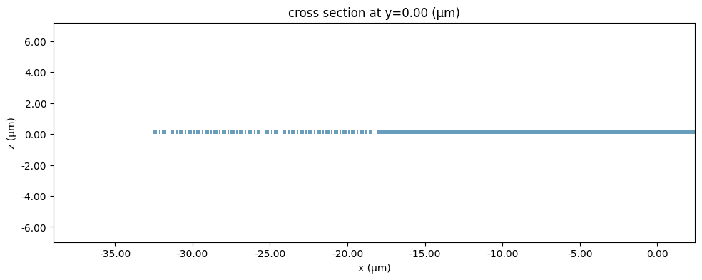
We can plot the geometry cross-section with the tidy3d_plot function.
[6]:
_, ax = plt.subplots(1, 1, figsize=(12, 4))
_ = pf.tidy3d_plot(gc, plot_type="structures", y=0, ax=ax)
Most PDK components will have appropriate ports or terminals for connections, and some will include pre-defined models for S parameter computation.
[7]:
y_splitter = siepic.component("ebeam_y_1550")
viewer(y_splitter)
[7]:

[8]:
y_splitter.ports
[8]:
{'P0': Port(center=(-7.4, 0), input_direction=0, spec=PortSpec(description="Strip TE 1550 nm, w=500 nm", width=1.5, limits=(-0.6, 0.82), num_modes=1, added_solver_modes=0, polarization="", target_neff=3.5, default_radius=0, path_profiles=[(0.5, 0, (1, 0))]), extended=True, inverted=False, bend_radius=0),
 'P1': Port(center=(7.4, -2.75), input_direction=180, spec=PortSpec(description="Strip TE 1550 nm, w=500 nm", width=1.5, limits=(-0.6, 0.82), num_modes=1, added_solver_modes=0, polarization="", target_neff=3.5, default_radius=0, path_profiles=[(0.5, 0, (1, 0))]), extended=True, inverted=False, bend_radius=0),
 'P2': Port(center=(7.4, 2.75), input_direction=180, spec=PortSpec(description="Strip TE 1550 nm, w=500 nm", width=1.5, limits=(-0.6, 0.82), num_modes=1, added_solver_modes=0, polarization="", target_neff=3.5, default_radius=0, path_profiles=[(0.5, 0, (1, 0))]), extended=True, inverted=False, bend_radius=0)}
[9]:
y_splitter.models
[9]:
{'Tidy3D': Tidy3DModel(run_time=None, medium=None, symmetry=(0, 0, 0), boundary_spec=None, monitors=(), structures=(), grid_spec=None, shutoff=None, subpixel=None, courant=None, port_symmetries=[('P1', 'P2', {'P0': 'P0', 'P2': 'P1'})], bounds=((None, None, None), (None, None, None)), source_gap=None, simulation_updates=None, autograd_config=None, verbose=True)}
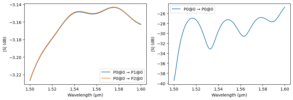
Running FDTD simulations
The Y splitter already has a Tidy3D model and waveguide ports, so a simple call to the s_matrix method is all that is needed to compute its S parameters.
[10]:
s_matrix_tidy3d = y_splitter.s_matrix(frequencies=td.C_0 / wavelengths)
Uploading task 'P0@0…'
Uploading task 'P1@0…'
Starting task 'P0@0': https://tidy3d.simulation.cloud/workbench?taskId=fdve-91edcb60-1cd4-4b0d-96cf-2b0a61e53e96
Starting task 'P1@0': https://tidy3d.simulation.cloud/workbench?taskId=fdve-8b9d3ed2-f5ba-4a02-a705-94d00f480563
Downloading data from 'P0@0'…
Downloading data from 'P1@0'…
Progress: 100%
[11]:
# Plot the S-parameters
_ = pf.plot_s_matrix(s_matrix_tidy3d, input_ports=["P0"], y="dB")
Running MODE simulations
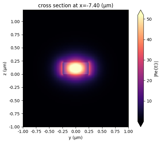
It is really easy to inspect port modes as well. The port_modes function will compute the modes and return a Tidy3D ModeSolver object with the mode data.
[12]:
mode_solver = pf.port_modes(
    y_splitter.ports["P0"],
    frequencies=[pf.C_0 / 1.5, pf.C_0 / 1.55, pf.C_0 / 1.6],
    mesh_refinement=40,
    group_index=True,
)
Uploading task 'Mode-ModeSolver…'Progress: 0% -
Starting task 'Mode-ModeSolver': https://tidy3d.simulation.cloud/workbench?taskId=mo-3b1c5464-d35b-4542-834d-ae09720a2aba
Downloading data from 'Mode-ModeSolver'…
Progress: 100%
[13]:
mode_solver.data.to_dataframe()
[13]:
| wavelength | n eff | k eff | loss (dB/cm) | TE (Ey) fraction | wg TE fraction | wg TM fraction | mode area | group index | dispersion (ps/(nm km)) | ||
|---|---|---|---|---|---|---|---|---|---|---|---|
| f | mode_index | ||||||||||
| 1.998616e+14 | 0 | 1.50 | 2.498887 | 0.0 | 0.0 | 0.985956 | 0.776479 | 0.820888 | 0.176755 | 4.178812 | 530.239525 |
| 1.934145e+14 | 0 | 1.55 | 2.442763 | 0.0 | 0.0 | 0.983523 | 0.763881 | 0.817728 | 0.190894 | 4.186544 | 509.816574 |
| 1.873703e+14 | 0 | 1.60 | 2.386398 | 0.0 | 0.0 | 0.980815 | 0.751972 | 0.814850 | 0.206530 | 4.193567 | 431.259422 |
[14]:
_ = mode_solver.plot_field("E", mode_index=0, f=pf.C_0 / 1.55)
Loading a GDSII file
Custom components can be loaded from GDSII files. We will load a phase shifter designed previously and available in the file thermo-optic_phase_shifter.gds.
To make sure the file is always available, the next cell creates the file automatically from its binary contents, so you do not need to download a separate file to run this notebook.
[15]:
import bz2
import pathlib

_ = pathlib.Path("thermo-optic_phase_shifter.gds").write_bytes(
    bz2.decompress(
        b"BZh91AY&SY\x91\x99q2\x00\x00/\xff\xff\xff\xff\xeeD$\x06\x80\xf16H@P\xaa\x06\xc4@\x00`\x00H@\x80\x00@\t\x02\x80\x04\x00D\x05\x10\xb0\x00\xf6"
        b"5\r\x12\x99\x06\x9a\x00\xd0\xd0\x00\x00\x07\xa8\x00\xd3\xc4\xd2\x06\x88\xa6\x9aa=@\xd3L\x80\x00\xd3CLF\x9a\x00\x00$RiM\xa9\x93FG\xea\x9a"
        b"\x06\x98\x04\x00\x00\x1a`hD\xbd\xe2\t\x93A`K\x99\x820\x10a\xab \x97\x0c\xa9D(\x94\x08\x91$\x11s\x1a\xd5\x14s\x19\xef\x8e\xc7\xd9UYd\x98\x1e"
        b"\xefp7`\x82\\\x87(\xe64\x83\xbc\x13UX\x81\x90\x8a\xa6A\xe9\xcd\x14t\x83\x04be\xecm\x17\xc52\x9e\xc5\xfa\xf8L,\xc6\xcc\x14\x01Q\xa3z\xdd\x04"
        b'\xca\xd3B\x87<*H\x89\x04j"\x86\x10\x82JpR\xeb\xae\xc2p\x9d\x004\x18\x97!\x04\x10\x0b\x89\xa5#\x80@\x9e\xc9{\x01\x04\xb4\xbc\x98\x81\x8bT^'
        b"\xd5\xbd\xc53W\x07\x18\x8c\xa6\x8d\x01N\x9d\x94\xd1l5\xedP\x15\xc0\xd8\x1bb#\xcd\xa2q\x82YN\x1bDl@\x8c :\xb5\x9c\xcf\x8f\x19\x8f\xe2\xeeH"
        b"\xa7\n\x12\x123.&@"
    )
)
With the file created, we can load in with the load_layout function. The loaded layout is a dictionary with all GDSII cells as components:
[16]:
components = pf.load_layout("thermo-optic_phase_shifter.gds")
components.keys()
[16]:
dict_keys(['top_cell'])
[17]:
phase_shifter = components["top_cell"]
viewer(phase_shifter)
[17]:

The GDSII format has no standard support for terminals, ports or models, so we have to add them after loading the geometry data:
[18]:
phase_shifter.terminals
[18]:
{}
[19]:
phase_shifter.ports
[19]:
{}
[20]:
phase_shifter.models
[20]:
{}
In most cases, we can automatically detect and add ports. If we know which port specification the geometry uses, we can use it to reduce the number of false positive results. In this case, we look for ports matching the “TE_1550_500” specification from the default technology.
[21]:
ports = phase_shifter.detect_ports(["TE_1550_500"])
ports
[21]:
[Port(center=(0, 0), input_direction=0, spec=PortSpec(description="Strip TE 1550 nm, w=500 nm", width=1.5, limits=(-0.6, 0.82), num_modes=1, added_solver_modes=0, polarization="", target_neff=3.5, default_radius=0, path_profiles=[(0.5, 0, (1, 0))]), extended=True, inverted=False, bend_radius=0),
 Port(center=(50, 0), input_direction=180, spec=PortSpec(description="Strip TE 1550 nm, w=500 nm", width=1.5, limits=(-0.6, 0.82), num_modes=1, added_solver_modes=0, polarization="", target_neff=3.5, default_radius=0, path_profiles=[(0.5, 0, (1, 0))]), extended=True, inverted=False, bend_radius=0)]
Both results are correct, so we can go ahead and add them:
[22]:
phase_shifter.add_port(ports)

viewer(phase_shifter)
[22]:

Being a straight waveguide, a semi-analytical waveguide model makes sense for this component.
[23]:
phase_shifter.add_model(pf.WaveguideModel(), "Waveguide")
[23]:
'Waveguide'
Terminals for electrical connection are represented by the 2 rectangles in layer (12, 0), “M2_router”. We can easily find them and add the appropriate terminals for routing later.
[24]:
for structure in phase_shifter.structures[12, 0]:
    phase_shifter.add_terminal(pf.Terminal("M2_router", structure))

viewer(phase_shifter)
[24]:

We can store the phase-shifter with the terminal, port and model information if we use a PhotonForge PHF file with the write_phf function:
[25]:
pf.write_phf("thermo-optic_phase_shifter.phf", phase_shifter)
Netlist-driven layout
We can now combine these PDK and custom components to form a cirucit for both layout and simulations. This can be done in an imperative way, by creating and connecting component references using the PhotonForge API, or in a declarative way, using a netlist to fully specify the circuit in a single object. The former approach can be seen in the Quantum Chip and LIDAR examples. Here we show the latter.
We set the defaults that will be used for routing and get the bounds information from the components we will use:
[26]:
pf.config.default_kwargs = {
    "radius": 10,
    "euler_fraction": 0.5,
}
[27]:
y_splitter.bounds()
[27]:
(array([-7.5, -3.5]), array([7.45, 3.5 ]))
[28]:
phase_shifter.bounds()
[28]:
(array([-13., -5.]), array([63., 15.]))
[29]:
def create_mzi(length=150, ps_y=25):
    netlist = {
        "name": "MZI",
        # Individual component instances
        "instances": {
            "yin": y_splitter,
            "yout": {"component": y_splitter, "origin": (length, 0), "rotation": 180},
            "ps": {"component": phase_shifter, "origin": (length / 2 - 25, ps_y)},
        },
        # Auto-routing
        "routes": [
            (("yin", "P2"), ("ps", "P0"), pf.parametric.route_s_bend),
            (("ps", "P1"), ("yout", "P1"), pf.parametric.route_s_bend),
            (("yin", "P1"), ("yout", "P2")),
        ],
        # External ports and terminals
        "ports": [("yin", "P0"), ("yout", "P0")],
        "terminals": [("ps", "T0"), ("ps", "T1")],
        # Model for the full circuit
        "models": [pf.CircuitModel()],
    }

    component = pf.component_from_netlist(netlist)
    return component


mzi = create_mzi()
viewer(mzi)
[29]:

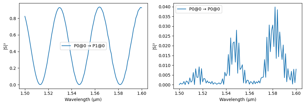
Circuit simulations
With the circuit model we added to the MZI, we can run circuit simulations by simply calling the s_matrix function again. PhotonForge will automatically run appropriate simulations for the sub-components to calculate the scattering matrix for the whole circuit.
[30]:
s_matrix_mzi = mzi.s_matrix(pf.C_0 / wavelengths)
Uploading task 'Mode-StripTE1550nmw500nm…'
Uploading task 'Mode-StripTE1550nmw500nm…'
Uploading task 'Mode-StripTE1550nmw500nm…'
Starting task 'Mode-StripTE1550nmw500nm': https://tidy3d.simulation.cloud/workbench?taskId=mo-27f321ae-7d8a-4688-b44d-1fc4226b2355
Downloading data from 'Mode-StripTE1550nmw500nm'…
Starting task 'Mode-StripTE1550nmw500nm': https://tidy3d.simulation.cloud/workbench?taskId=mo-25ae685f-0a59-49a8-8e61-1fc565f53ab1
Downloading data from 'Mode-StripTE1550nmw500nm'…
Starting task 'Mode-StripTE1550nmw500nm': https://tidy3d.simulation.cloud/workbench?taskId=mo-1aa8bec2-ebe4-4aa1-9cde-f8bd2d178b30
Downloading data from 'Mode-StripTE1550nmw500nm'…
Progress: 100%
[31]:
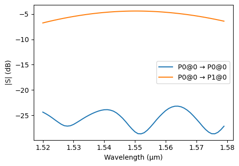
_ = pf.plot_s_matrix(s_matrix_mzi, input_ports=["P0"])
Adding GCs for layout
Just as before, we use a netlist to describe the circuit with the grating couplers from the PDK. This function will use the MZI as argument so that we can vary its parameters later when creating the full chip.
[32]:
def mzi_with_gratings(mzi, fiber_spacing=127, spacing_y=50):
    netlist = {
        "name": "MZI_with_GC",
        "instances": {
            "mzi": {"component": mzi, "origin": (0, spacing_y), "rotation": 90},
            "gc1": {"component": gc, "origin": (0, 0), "rotation": 90},
            "gc2": {"component": gc, "origin": (fiber_spacing, 0), "rotation": 90},
        },
        "routes": [
            (("gc1", "P0"), ("mzi", "P0")),
            (("mzi", "P1"), ("gc2", "P0"), {"radius": fiber_spacing / 2.0}),
        ],
        "ports": [("gc1", "P1"), ("gc2", "P1")],
        "terminals": [("mzi", "T0"), ("mzi", "T1")],
        "models": [pf.CircuitModel()],
    }

    component = pf.component_from_netlist(netlist)
    return component


mzi_gratings = mzi_with_gratings(mzi)

viewer(mzi_gratings)
[32]:

Instead of simulating the grating coupler in Tidy3D, we will show how to use pre-computed or measured data to avoid the large simulations.
The Touchstone file ebeam_gc_te1550.sp2 contains example data we can load and assign to the grating coupler with a data model, which could have come from previous measurements, for example.
As with the GDSII file we used previously, we will re-create the Touchstone file from its contents so you don’t have to download it separately.
[33]:
_ = pathlib.Path("ebeam_gc_te1550.s2p").write_text("""[Version] 2.0
# Hz S RI
[Number of Ports] 2
[Two-Port Data Order] 12_21
[Number of Frequencies] 31
[Network Data]
1.897421e+14 -0.0352072 0.0326903 -0.226435 -0.447915 0.210738 0.421143 0.00676895 0.0264931
1.899825e+14 -0.0396145 0.00837585 -0.0362153 -0.512323 0.0336372 0.484589 0.00360995 0.0245064
1.902236e+14 -0.0354181 -0.010244 0.169495 -0.496585 -0.161001 0.47345 0.00310874 0.0214094
1.904653e+14 -0.026563 -0.0276462 0.357034 -0.398698 -0.341562 0.383859 0.00534486 0.0196147
1.907077e+14 -0.00635631 -0.0433821 0.493656 -0.230711 -0.47628 0.225361 0.00848205 0.0208979
1.909506e+14 0.0271043 -0.0439097 0.553475 -0.0179504 -0.538816 0.0205268 0.00983997 0.0250636
1.911942e+14 0.0573636 -0.016617 0.523126 0.20503 -0.513759 -0.198027 0.00772578 0.0298957
1.914384e+14 0.0591343 0.0296758 0.404572 0.400752 -0.400509 -0.392852 0.00269386 0.0325817
1.916832e+14 0.0241182 0.0647929 0.214641 0.535193 -0.214451 -0.52857 -0.00274075 0.0316472
1.919286e+14 -0.0260546 0.0625573 -0.0171573 0.582968 0.0150289 -0.578581 -0.0057533 0.0280115
1.921747e+14 -0.0569269 0.0256378 -0.252092 0.532182 0.249155 -0.53042 -0.00514607 0.0244794
1.924213e+14 -0.0517625 -0.0175119 -0.448512 0.38844 0.44637 -0.388954 -0.00231797 0.0238635
1.926687e+14 -0.0230183 -0.04036 -0.570368 0.175072 0.570088 -0.17651 -0.000417023 0.0269198
1.929166e+14 0.00586192 -0.0394758 -0.594637 -0.0712344 0.596004 0.0705136 -0.00209928 0.031656
1.931652e+14 0.0243362 -0.0276428 -0.515563 -0.307241 0.517319 0.308136 -0.00752106 0.034704
1.934145e+14 0.0364941 -0.0125098 -0.345937 -0.490763 0.34663 0.492995 -0.0141874 0.0337846
1.936644e+14 0.0435652 0.00978416 -0.115382 -0.588478 0.114132 0.59075 -0.0187811 0.0293522
1.939149e+14 0.0348038 0.0393164 0.135057 -0.582551 -0.137855 0.583101 -0.0195603 0.0241891
1.941661e+14 0.0019319 0.0592741 0.360515 -0.473915 -0.363013 0.471707 -0.0175394 0.0213398
1.944179e+14 -0.041254 0.0478519 0.520442 -0.282017 -0.520386 0.27783 -0.01565 0.0219132
1.946704e+14 -0.0635397 0.00473916 0.585755 -0.0419279 -0.582075 0.0380054 -0.0165477 0.0243395
1.949236e+14 -0.0456419 -0.0414984 0.545159 0.201759 -0.538441 -0.203066 -0.0206354 0.0255948
1.951774e+14 -0.000953603 -0.0582347 0.407918 0.404146 -0.399799 -0.401147 -0.0258056 0.0235307
1.954319e+14 0.0376615 -0.0388482 0.201359 0.529297 -0.194252 -0.521024 -0.0291419 0.0184768
1.956870e+14 0.0494522 -0.00407037 -0.0353287 0.556626 0.0382115 -0.54334 -0.0291566 0.0128121
1.959428e+14 0.0390625 0.0235674 -0.25862 0.483795 0.254042 -0.467837 -0.0267002 0.00903373
1.961993e+14 0.020525 0.0388267 -0.428387 0.326759 0.414603 -0.312517 -0.0240809 0.00801482
1.964564e+14 -0.00202446 0.0458016 -0.515291 0.116663 0.493245 -0.10946 -0.0232984 0.00859377
1.967142e+14 -0.0303964 0.0403233 -0.506173 -0.106335 0.479893 0.101871 -0.0246625 0.00861082
1.969727e+14 -0.0543518 0.0125664 -0.406116 -0.300777 0.382185 0.282568 -0.0267262 0.0065854
1.972319e+14 -0.0515758 -0.031471 -0.237294 -0.431789 0.223014 0.401693 -0.0275304 0.00276416
[End]""")
With the file created, we can load it as an S matrix object and use it to create the data model.
[34]:
s_matrix_data = pf.SMatrix.load_snp("ebeam_gc_te1550.s2p")
data_model = pf.DataModel(s_matrix_data, interpolation_method="akima")

_ = gc.add_model(data_model, "Data")
[35]:
_ = pf.plot_s_matrix(gc.s_matrix(pf.C_0 / wavelengths), y="dB", input_ports=["P0"])
Progress: 100%
[36]:
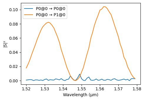
s_matrix_mzi_gratings = mzi_gratings.s_matrix(pf.C_0 / wavelengths)
_ = pf.plot_s_matrix(s_matrix_mzi_gratings, input_ports=["P0"])
Uploading task 'Mode-StripTE1550nmw500nm…'
Uploading task 'Mode-StripTE1550nmw500nm…'
Uploading task 'Mode-StripTE1550nmw500nm…'
Starting task 'Mode-StripTE1550nmw500nm': https://tidy3d.simulation.cloud/workbench?taskId=mo-b9e3ab0e-3364-4046-9cea-1fef0b7b61fa
Starting task 'Mode-StripTE1550nmw500nm': https://tidy3d.simulation.cloud/workbench?taskId=mo-036d88dc-5ed8-4e84-aa79-1a48530ad3e6
Downloading data from 'Mode-StripTE1550nmw500nm'…
Downloading data from 'Mode-StripTE1550nmw500nm'…
Starting task 'Mode-StripTE1550nmw500nm': https://tidy3d.simulation.cloud/workbench?taskId=mo-41275651-06de-441b-902b-423fd657ba59
Downloading data from 'Mode-StripTE1550nmw500nm'…
Progress: 100%
Electrical connections
For the electrical connections we add bond pads to the final layout.
[37]:
tech.layers
[37]:
| Name | Layer | Description | Color | Pattern |
|---|---|---|---|---|
| Si | (1, 0) | SiEPIC - Waveguide | #ff80a818 | \\ |
| PinRec | (1, 10) | SiEPIC | #ff80a818 | xx |
| PinRecM | (1, 11) | SiEPIC | #80000018 | + |
| Si Slab | (2, 0) | Dedicated Run Layers - Device…… Layer Partial Etch | #c080ff18 | / |
| Direct Metal | (5, 0) | Dedicated Run Layers | #80a8ff18 | || |
| Oxide open to BOX | (6, 0) | Dedicated Run Layers | #ff000018 | - |
| Text | (10, 0) | Text-Not Fabricated | #00000018 | hollow |
| M1_heater | (11, 0) | TiW Heater | #0000ff18 | \\ |
| M2_router | (12, 0) | TiW/Au Routing Bilayer | #ffbf0018 | // |
| M_Open | (13, 0) | Bond Pad Open | #80005718 | \\ |
| Si n | (20, 0) | Dedicated Run Layers | #afff8018 | - |
| Si p | (21, 0) | Dedicated Run Layers | #ffd9df18 | = |
| Si n+ | (22, 0) | Dedicated Run Layers | #ff800018 | x |
| Si p+ | (23, 0) | Dedicated Run Layers | #ddff0018 | xx |
| Si n++ | (24, 0) | Dedicated Run Layers | #00ffff18 | + |
| Si p++ | (25, 0) | Dedicated Run Layers | #00800018 | ++ |
| ANT Reserved | (31, 0) | SiEPIC/ANT Reserved | #9580ff18 | / |
| ANT Reserved 1 | (33, 0) | ANT Reserved | #9580ff18 | / |
| Via to silicon | (40, 0) | Dedicated Run Layers | #0000ff18 | . |
| DevRec | (68, 0) | SiEPIC | #00800018 | . |
| FbrTgt | (81, 0) | SiEPIC/Dedicated Run Layers | #80808018 | ++ |
| ANT Reserved 2 | (102, 0) | ANT Reserved | #9580ff18 | / |
| ANT Reserved 3 | (110, 0) | ANT Reserved | #9580ff18 | / |
| Custom Dicing | (189, 0) | #00000018 | hollow | |
| SEM Imaging | (200, 0) | #ff000018 | x | |
| Deep Trench | (201, 0) | #00ff0018 | . | |
| Deep Trench Handling Exclusion | (202, 0) | #00760018 | : | |
| Thermal Isolation Trenches | (203, 0) | #00800018 | \ | |
| Laser Integration Shelf | (205, 0) | Dedicated Run Layers | #69ff0518 | xx |
| Floor Plan-Not Fabricated | (290, 0) | #c080ff18 | hollow | |
Error: device layer width is…… less than design rule | (301, 0) | DRC Errors | #80005718 | = |
Error: device layer spacing is…… less than design rule | (301, 1) | DRC Errors | #80005718 | - |
Warning: polygons/paths on…… PinRec layer (1/10) will NOT be fabricated | (301, 2) | DRC Errors | #80005718 | || |
Error: direct metal width is…… less than 5 microns | (305, 0) | DRC Errors | #80808018 | ++ |
Error: direct metal spacing is…… less than 10 microns | (305, 1) | DRC Errors | #80808018 | + |
Error: TiW width is less than 3…… microns | (311, 0) | DRC Errors | #ffa08018 | // |
Error: TiW spacing is less than…… 3 microns | (311, 1) | DRC Errors | #ffa08018 | / |
Error: Al width is less than…… design rule | (312, 0) | DRC Errors | #00ffff18 | | |
Error: Al spacing is less than…… design rule | (312, 1) | DRC Errors | #00ffff18 | // |
Error: Spacing between TiW and…… Al is less than 5 microns | (312, 3) | DRC Errors | #00ffff18 | \\ |
Error: Oxide window width is…… less than 10 microns | (313, 0) | DRC Errors | #01ff6b18 | || |
Error: Oxide window spacing is…… less than 10 microns | (313, 1) | DRC Errors | #01ff6b18 | | |
Error: Oxide window is not…… placed over Al | (313, 2) | DRC Errors | #01ff6b18 | // |
| Standard Design Area | (350, 0) | DRC Errors | #ddff0018 | \ |
Error: Features outside design…… area. Verify design size and centering. | (350, 1) | DRC Errors | #ddff0018 | : |
Error: Dicing lane width is…… less than 100 microns | (389, 0) | DRC Errors | #ff00ff18 | ++ |
Error: Spacing between dicing…… lane and devices is less than 50 microns | (389, 1) | DRC Errors | #ff00ff18 | + |
Error: SEM width is less than…… 500 nm | (400, 0) | DRC Errors | #ff9d9d18 | x |
| Deep Trench Design Area | (401, 0) | DRC Errors | #80a8ff18 | xx |
Error: Metal, SEM, or handling…… region overlap with deep trenches. Verify design centering | (401, 1) | DRC Errors | #80a8ff18 | x |
Warning: Silicon features…… outside deep trench design area. Verify accuracy before submission | (401, 2) | DRC Errors | #80a8ff18 | = |
Error: Spacing between metal…… and deep trench is less than 30 microns | (401, 3) | DRC Errors | #80a8ff18 | - |
Error: Deep trench width is…… less than 260 microns | (401, 4) | DRC Errors | #80a8ff18 | || |
Error: Deep trench handling…… area missing. Please add handling area of size shown by polygons | (402, 0) | DRC Errors | #ff000018 | + |
Error: Features inside deep…… trench handling area | (402, 1) | DRC Errors | #ff000018 | xx |
Error: Thermal isolation width…… is less than design rule | (403, 0) | DRC Errors | #50008018 | ++ |
Error: Thermal isolation…… spacing is less than design rule | (403, 1) | DRC Errors | #50008018 | + |
Error: Spacing between thermal…… isolation and metal is less than design rule | (403, 2) | DRC Errors | #50008018 | xx |
Error: Thermal isolation and…… device layer overlap, or spacing is less than design rule | (403, 3) | DRC Errors | #50008018 | x |
Dream Photonics Black Box-Not…… Fabricated | (998, 0) | #00000018 | hollow | |
| Errors | (999, 0) | SiEPIC | #0000ff18 | || |
[38]:
bp = pf.Component("BondPad")
bp.add_terminal(pf.Terminal("M2_router", pf.Rectangle(size=(100, 100))), add_structure=True)
bp.add("M_Open", pf.Rectangle(size=(95, 95)))
viewer(bp)
[38]:

[39]:
def mzi_with_bond_pads(mzi, bp_x=-250, bp_y=500, bp_spacing=150):
    netlist = {
        "name": "Circuit",
        "instances": {
            "mzi": mzi_with_gratings(mzi),
            "bp1": {"component": bp, "origin": (bp_x, bp_y)},
            "bp2": {"component": bp, "origin": (bp_x + bp_spacing, bp_y)},
        },
        "terminal routes": [
            (("mzi", "T0"), ("bp1", "T0"), {"width": 30, "overlap_fraction": 0.5}),
            (("mzi", "T1"), ("bp2", "T0"), {"width": 30, "overlap_fraction": 0.5}),
        ],
        "ports": [("mzi", "P0"), ("mzi", "P1")],
        "terminals": [("bp1", "T0"), ("bp2", "T0")],
        "models": [pf.CircuitModel()],
    }

    component = pf.component_from_netlist(netlist)
    return component


mzi_bp = mzi_with_bond_pads(mzi)
viewer(mzi_bp)
[39]:

Final chip layout
We can now easily repeat this design (or variations of it) to build the final layout.
We will vary the MZI parameters to create a few variations:
[40]:
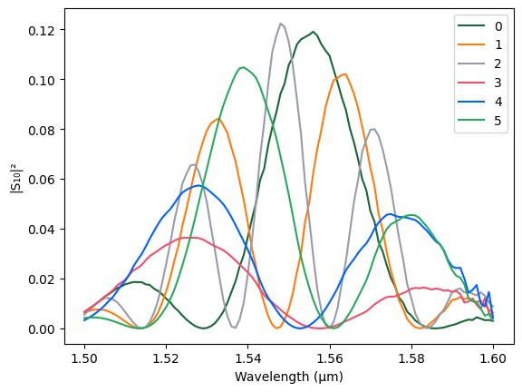
variations = []

for length in [150, 250]:
    for ps_y in [20, 25, 30]:
        # Create the variation
        base_mzi = create_mzi(length=length, ps_y=ps_y)
        variation = mzi_with_bond_pads(base_mzi)

        # Add a label to identify the device (this could be done in the create_mzi
        # or any other component creation function directly too)
        variation_id = f"L: {length}\nY: {ps_y}"
        variation.add("Text", *pf.text(variation_id, size=50, origin=(-200, 20)))
        variations.append(variation)

viewer(variations[0])
[40]:

[41]:
_, ax = plt.subplots(1, 1)
for i, variation in enumerate(variations):
    s = variation.s_matrix(pf.C_0 / wavelengths, show_progress=False)
    ax.plot(s.wavelengths, np.abs(s["P0@0", "P1@0"]) ** 2, label=str(i))

ax.set(xlabel="Wavelength (μm)", ylabel="|S₁₀|²")
_ = ax.legend()
[42]:
main = pf.Component("MZM_PIC")

for i, variation in enumerate(variations):
    var_ref = pf.Reference(variation, origin=(600 * i, 0))
    main.add(var_ref)

# Add device region
chip_bounds = pf.envelope(main, 200, use_box=True)
main.add("DevRec", chip_bounds)

# Export the final geometry to a GDSII file
main.write_gds("MZM_PIC.gds")

viewer(main)
/tmp/ipykernel_987362/2326998191.py:12: RuntimeWarning: The following components have been renamed in the layout because all names must be non-empty and unique: 'Circuit_1', 'MZI_1', 'MZI_2', 'MZI_with_GC_1', 'Circuit_2', 'MZI_3', 'MZI_with_GC_2', 'MZI_4', 'MZI_with_GC_3', 'Circuit_3', 'Circuit_4', 'Circuit_5', 'MZI_with_GC_4', 'MZI_with_GC_5', 'MZI_5'.
  main.write_gds("MZM_PIC.gds")
[42]:
