Frequently Asked Questions
The first sections answer questions about PhotonForge as a product. The last section, Python API, answers questions about the Python API.
What PhotonForge Is
What is PhotonForge?
PhotonForge 2.0 is an end-to-end design automation platform for photonic integrated circuits. It covers the full design flow: the PDK, components, device simulation, the schematic, layout and routing, circuit simulation, verification, and version control of the design and its data. It is a Python package with a local GUI, and it uses Tidy3D for device simulation. The front page follows one chip through every step.
How do I start?
Install PhotonForge with one command:
pip install photonforge.Read Key Concepts for the main ideas: components, technologies, ports and models.
Follow Quick Start I. It builds a circuit in the local GUI and simulates it, at no cost.
Follow Quick Start II. It builds and simulates a passive circuit on an open PDK in Python.
Follow Quick Start III. It makes the circuit active and simulates a transmitter link.
You need a free Tidy3D account only when you run Tidy3D simulations.
PDKs
What does PDK support mean in PhotonForge?
A PDK for PhotonForge is a Python package with two parts:
A technology: the layers, the layer stack (the thickness and material of each layer) and the waveguide cross sections.
A library of parametric cells. Each cell has a layout and a model for circuit simulation.
When a PDK is installed, its cells show in the library of the local GUI. You can simulate any cell in Tidy3D directly from its layout, because the technology gives the 3D structure. DRC uses the rule deck from the foundry.
Which foundries are available?
Open PDKs: SiEPIC (EBeam silicon and silicon nitride), Luxtelligence (LNOI400 and LTOI300) and Cornerstone. Foundry PDKs: GlobalFoundries, Tower Semiconductor, AIM Photonics, imec, AMF, Ligentec, Fraunhofer HHI and SMART Photonics. The PDKs table on the front page shows how to install the open PDKs.
How do I get access to the PDKs?
Open PDKs install with pip.
Foundry PDKs come with PhotonForge Enterprise, and you also need your own NDA with the foundry.
Contact us to get access to a foundry PDK.
How does PhotonForge work with existing EDA tools?
Layouts import and export as GDS and OASIS files (Importing a GDSII/OASIS Layout, Exporting a GDSII/OASIS Layout).
The Cadence connector reads PDK cells, parametric cells and schematics from Virtuoso, and writes the finished layout back for Check Against Source.
DRC and LVS connectors run the foundry rule decks.
Compact models export to Verilog-A for SPICE simulators.
Contact us to set up the EDA connectors.
Are compact models available?
Yes. Each cell in a PhotonForge PDK comes with a model. PhotonForge also has a library of analytic and time-domain models: waveguides, couplers, rings, MZIs, modulators, lasers, amplifiers and photodiodes. For system design before you have a layout, the Abstract Components blocks give the same models without a layout. See Compact Models and Time Domain Models.
How is verification done?
DRC checks the layout against the foundry rule deck. LVS extracts the optical and electrical connections from the layout and compares them with the schematic. See Verification.
How do I build my custom PDK?
Define a technology in Python: the layers, the layer stack and the waveguide cross sections (Custom Technology).
Write the cells as parametric components and attach their models (Custom Parametric Components).
Share the PDK as a Python package, or as a library in Photonic Canvas (Photonic Design Automation).
The Technology and PDK Setup and Custom Component Library examples build a complete PDK for a datacom chip.
AI Agents
What makes PhotonForge agentic?
Three things make PhotonForge work well with AI agents:
Every step is a Python call: build cells, place and route, simulate, and run DRC. An AI coding agent can do all of them.
Skill files teach the agent how to do each task with PhotonForge, and a documentation server gives it the current API. The PhotonForge plugin installs both in the AI tool you use.
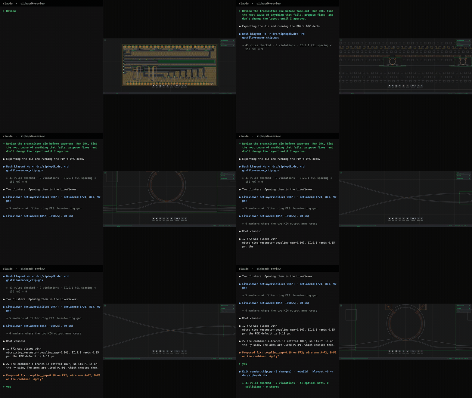
The local GUI is built for agents as well as people. An agent can open a design in the GUI, look at it and edit it, and you see each change on your screen. When you edit the design in the GUI, the agent reads your changes and continues from them.
How do I use AI to design my photonic chip?
Install the PhotonForge plugin in your AI coding tool (see AI Agents).
Tell the agent what you want, in plain words. For example: “Place five ring modulators on one bus at the channel radii and route each heater to a pad.”
Look at the result in the local GUI. Edit it there if you want, then ask for the next step.
The agent writes a Python script, so you can read, change and run the design again.
What are skill files?
A skill file is a set of instructions that teaches an AI agent one task. The PhotonForge plugin installs skills for these tasks: parametric cells, layout and connectivity checks, circuit and time-domain simulation, the local GUI, project versioning, file formats, and yield analysis. The agent loads a skill when the task needs it.
What is an MCP server?
MCP (Model Context Protocol) is a standard way for an AI agent to use tools. The PhotonForge plugin installs an MCP server that searches and reads the PhotonForge and Tidy3D documentation, so the agent works from the current API.
Which tool should I use: VS Code, Cursor, Claude Code or Codex?
Use the tool your team already uses. The plugin installs in Claude Code, Codex, Cursor, VS Code and Copilot.
What is autonomous PIC design?
In autonomous design, an agent runs the design loop by itself: it changes the design, simulates it, checks the rules, keeps what improves the result, and repeats. We use agent loops to optimize components and to build complete chip layouts. Our paper Autonomous agentic design for photonics describes the method and its results. The design-loop template is open source: autophotonicdesign. Contact us if you want to try it on your design.
Components
How do I create a component? Can I do it in Python?
Yes. A component holds shapes on the PDK layers, ports and models. Build it from shapes and paths, from other components, or from a GDS file. See Components, Ports and Importing a GDSII/OASIS Layout.
How do I make it parametric?
Write a function that builds the component from its arguments, and add the parametric_component() decorator:
import photonforge as pf

pf.config.default_technology = pf.basic_technology()

@pf.parametric_component
def heater(*, length: float = 100, width: float = 2):
    """A metal heater strip."""
    component = pf.Component()
    component.add("METAL", pf.Rectangle(center=(0, 0), size=(length, width)))
    return component

short_heater = heater(length=50)
The component remembers its parameters, so you can change them later and rebuild it. See Custom Parametric Components.
How do I connect components to make a circuit?
In the local GUI:
Drag the cells from the Component Library onto the schematic.
Draw a wire from one port to another.
Press Place to put the cells on the chip, then Route to draw the waveguides.
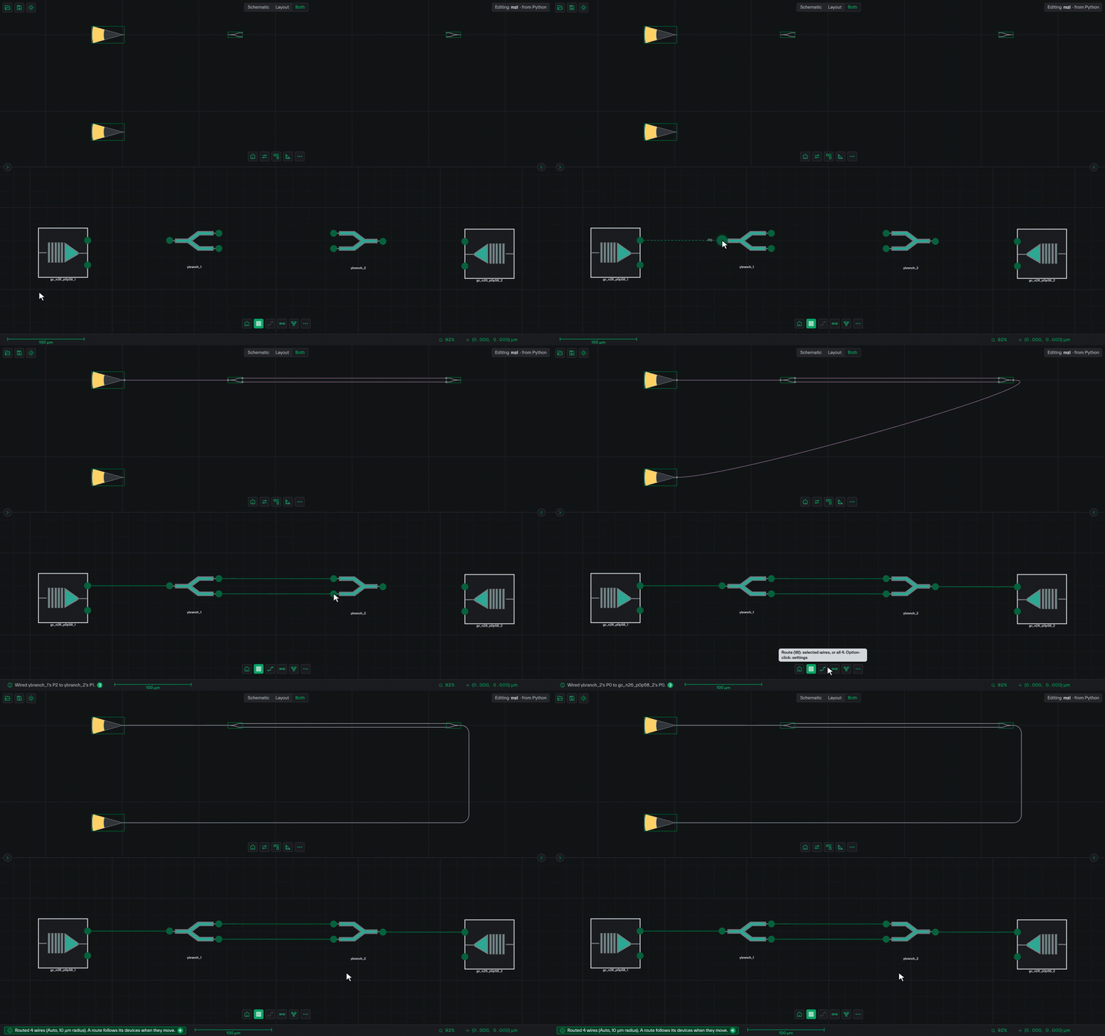
In Python, connect two ports directly, route a waveguide between them, or write the circuit as a netlist with component_from_netlist().
The front page has a netlist example.
See Routing and Connections and Circuit Model.
How do I define custom models for my component?
Start with a built-in model and set its values, or use data from a simulation or a measurement (Data Model). For a new device, write your own model class for the frequency domain or the time domain (Custom Model, Custom Expressions).
How do I run component-level simulations?
Attach a Tidy3DModel (FDTD) or an EMEModel to the component and ask for its S parameters.
PhotonForge builds the simulation from the layout and the PDK layer stack.
Check the cost before the run: see How to estimate the cost of an S matrix computation?.
The Getting Started page and Tidy3D Model show the steps.
Circuits and Chips
How do I define netlists?
A netlist is a Python dictionary.
It lists the instances, the connections between ports, the virtual connections (links that a route makes later), the routes, and the top-level ports.
component_from_netlist() turns it into a component.
A schematic drawn in the local GUI makes the same netlist.
Netlists from other tools convert to this format: the Cadence connector reads Virtuoso schematics, and a short script, which an AI agent can write for you, converts other formats such as a gdsfactory netlist.
See Foundry-Compatible PIC Design Flow and Layout vs. Schematic (LVS).
Can I import netlists from other EDA tools, or export them?
The Cadence connector reads Virtuoso schematics. Models and circuits export to Verilog-A for SPICE simulators. Layouts move as GDS and OASIS files, and PhotonForge reads S parameters from Touchstone files.
How do I run circuit simulations?
Add a CircuitModel to the circuit and ask for its S parameters.
PhotonForge combines the model of every component into the response of the circuit.
Circuit simulations run on your computer.
See Circuit Model and Cascaded Rings Filter.
Can I run time-domain and frequency-domain simulations?
Yes. In the frequency domain you get the S parameters over wavelength. In the time domain you drive the circuit with signals, such as a bit pattern on a modulator, and get waveforms and eye diagrams. See Time Domain Models and Time-Domain Simulation of a Mach–Zehnder Interferometer.
How do I run system-level electronic-photonic simulations?
Electrical parts (signal sources, drivers, transmission lines, amplifiers and filters) go into the same circuit as the optical parts. To simulate with your own electronic circuits, export the photonic models to Verilog-A and run them in SPICE. See Signal Integrity Analysis of a 100 Gbps Transmitter and Series Push-Pull Mach-Zehnder Modulator with Slow-Wave T-Rail Electrodes.
Can I do schematic-driven layout?
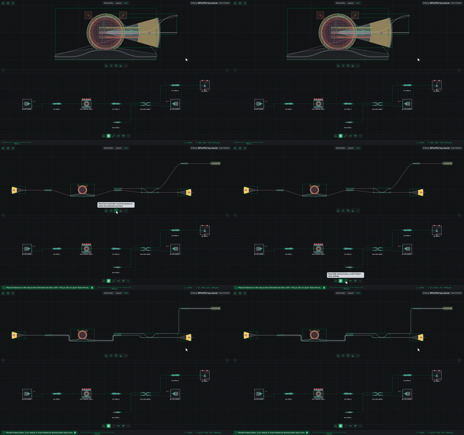
Yes. Draw the schematic in the local GUI, or load it from Python. Place the cells on the chip from the schematic, then route the wires. The layout keeps the connections of the schematic, so LVS can compare the two.
Layout and Routing
Can PhotonForge handle realistic layouts?
Yes. The examples include full chips with hundreds of cells and thousands of routes, and the local GUI opens very large layout files. This hexagonal programmable processor, after a published design, fills a 32 mm by 10 mm die with hundreds of optical and electrical routes:
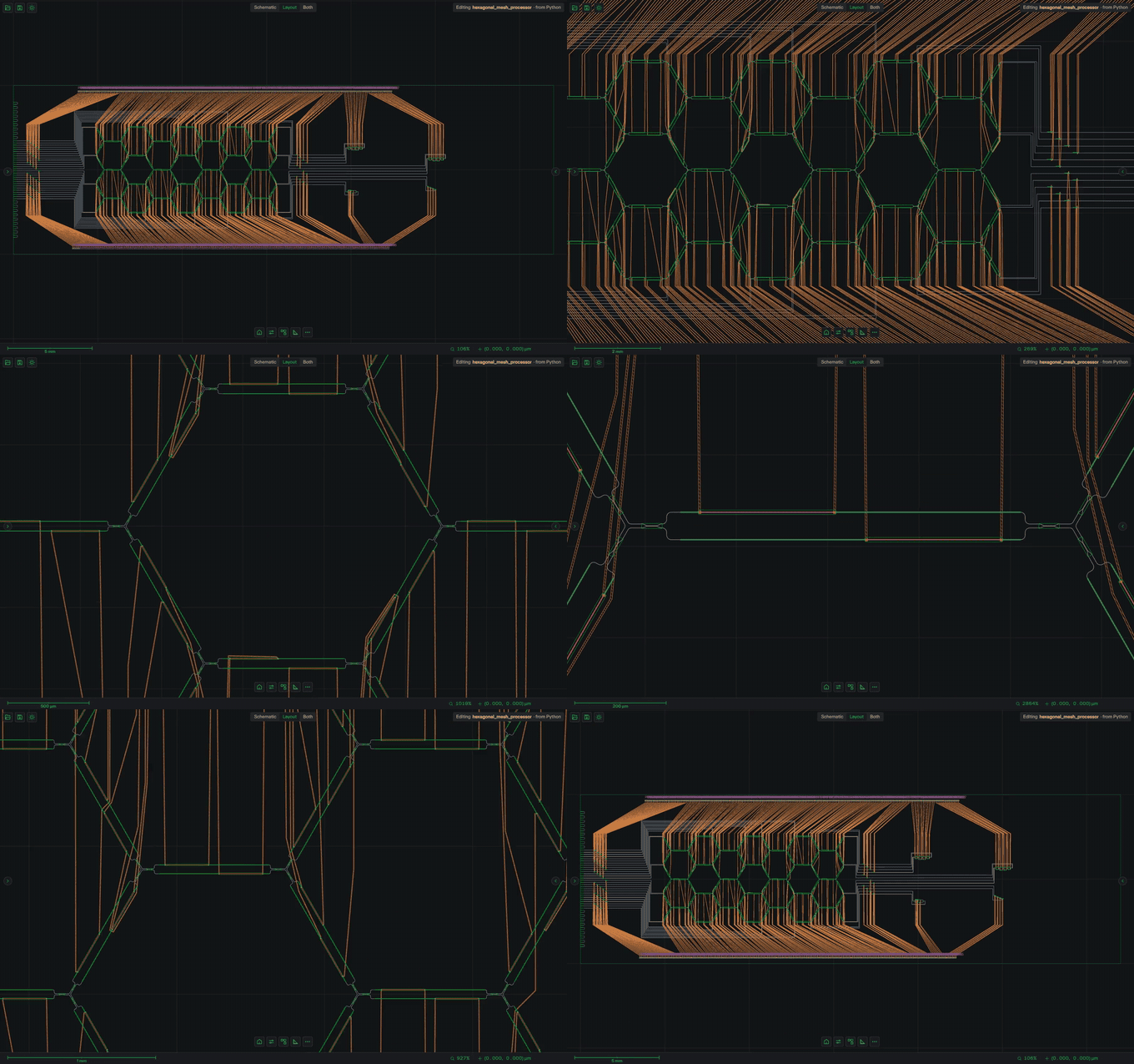
See Full chip layout, Chip Layout and Quantum Chip Layout.
Is there autorouting in PhotonForge?
Yes.
parametric.route_auto() routes many nets in one call.
It uses the bend radius you give and avoids the cells on the chip.
See Auto Routing.
Can it do path-length matching?
Yes.
Add matching=[pf.PathLengthMatching()] to the router, and it adds meanders until the routes have equal lengths.
A single route can also have a target length.
The front page has an example.
Can it avoid obstacles?
Yes. The cells on the chip are obstacles, and you can add keep-out shapes.
Can I route a bundle of nets?
Yes. Give the router a list of start ports and a list of end ports. It routes the bundle together and keeps the order of the nets.
Can optical routes add crossings automatically?
Yes. When two nets must cross, the router places a waveguide crossing cell. You choose the crossing cell and the maximum number of crossings.
Can I use my own bends and straight sections in autorouting?
Yes. Give the router the bend and straight cells from your PDK, and it uses them for every route.
Can I route electrical traces with vias?
Yes. The electrical router connects terminals and pads on the metal layers of the PDK. It adds a via where a trace changes metal layer.
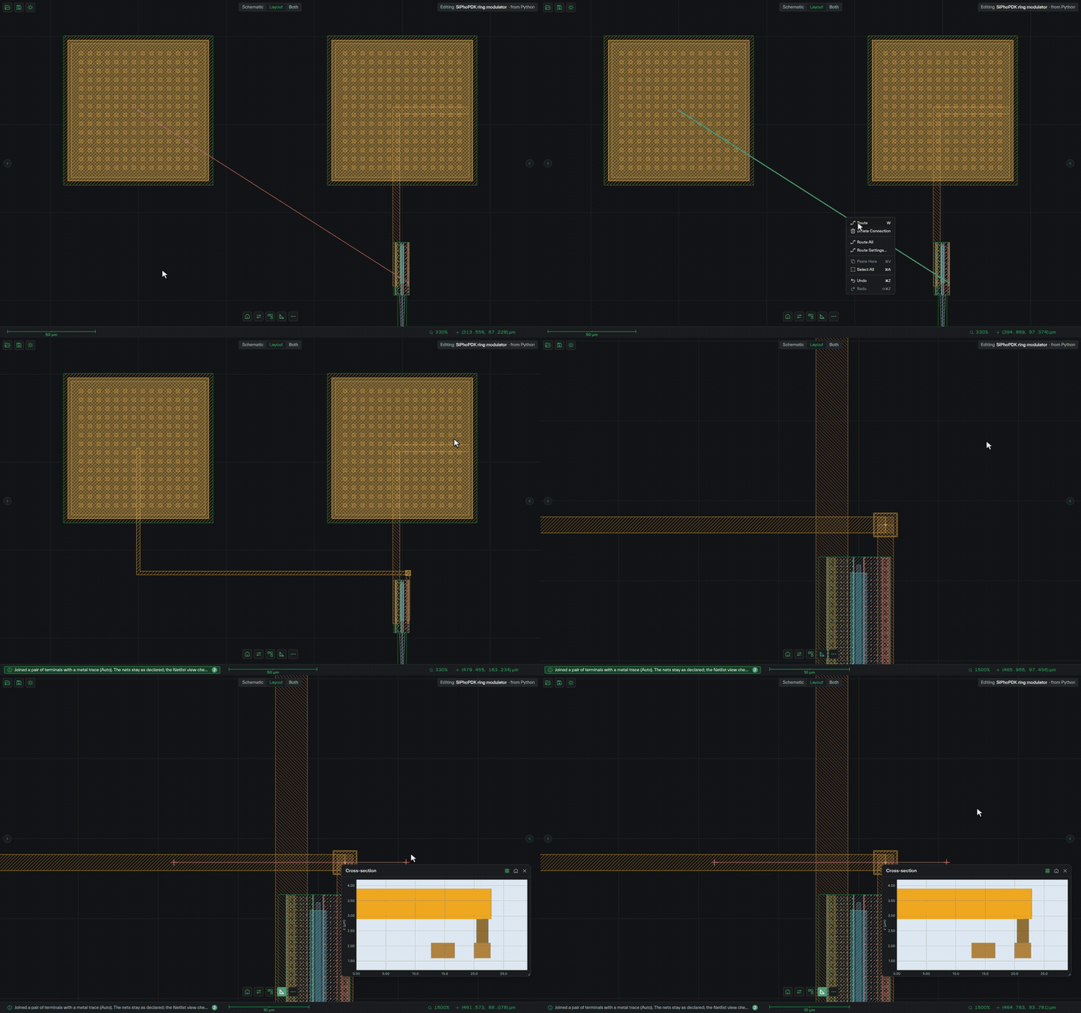
Can I do optical and electrical connectivity checks?
Yes. PhotonForge extracts the optical and electrical connections from the layout geometry. It finds open nets, shorts between nets, and routes that collide. See Layout vs. Schematic (LVS).
More on Simulation
How does circuit simulation use device simulation results?
The model of a component can come from its Tidy3D simulation. The circuit then uses those S parameters, so the circuit response follows the real geometry. See Building Circuit Models from Layout Files and Cascaded Rings Filter.
How do I optimize individual components?
Use inverse design: PhotonForge gets the gradient of the S parameters with respect to the parameters of a cell from Tidy3D, and an optimizer changes the cell. See Inverse Design with Autograd, Inverse Designed Grating Coupler and Inverse Design of a Fabrication-Robust Bent Directional Coupler.
Can I run circuit-level optimization?
Yes, with any Python optimizer: change the circuit parameters, such as a ring radius or a bias, and run the circuit simulation again. Circuit simulations run on your computer, so each step is fast. Gradients through the circuit simulation are not available yet.
Can I simulate nonlinear active and passive devices?
Yes, in the time domain. The models include optical amplifiers with gain saturation, electro-absorption modulators, and waveguides and rings with the Kerr effect, two-photon absorption, free carriers and heating. See Time Domain Models and Self Pulsing in Silicon Microring Resonator.
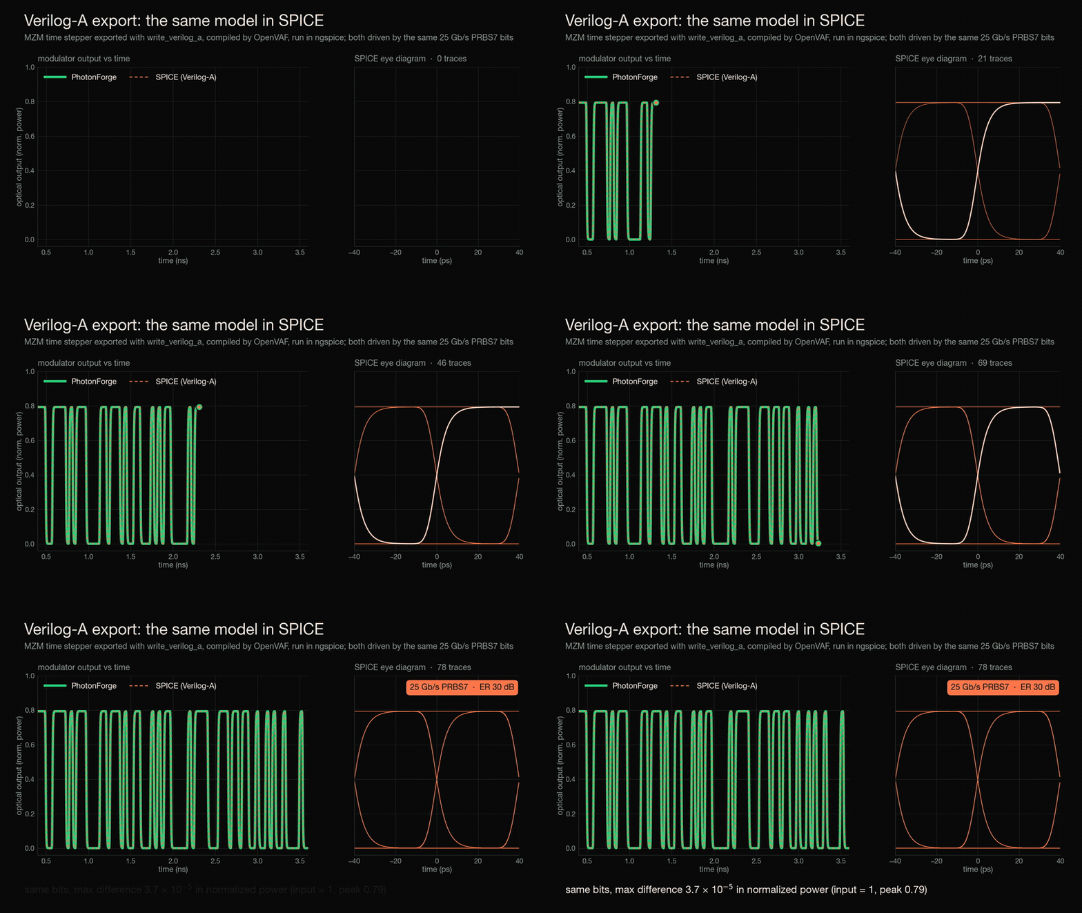
Can PhotonForge generate Verilog-A compact models automatically?
Yes. A time-domain model, or a whole circuit, exports to a Verilog-A model that runs in SPICE simulators. The output of the exported model agrees with the PhotonForge simulation.
How do I include fabrication variation in my simulation?
Set the process parameters, such as waveguide width and film thickness, as random variables and run a Monte Carlo simulation (Monte Carlo). The results show the spread of the circuit response and the yield. See Fabrication-Aware Simulation: Two Coupled Ring Resonator Filter and Waveguide Crossing Yield Analysis.
Can I simulate a nonlinear microring?
Yes. The nonlinear ring model includes heating, free carriers and the Kerr effect, so it shows thermal bistability and self-pulsing. See Self Pulsing in Silicon Microring Resonator.
How do I build multiphysics models for my component?
PhotonForge builds the 3D structures of a component from its layout, including the doping. Run the Tidy3D charge solver for the carriers in a junction and the heat solver for the temperature of a heater. Use the change in refractive index in the optical simulation and in the compact model. See 3D doping extrusion from a 2D carrier profile and Two-Segment Silicon Microring Modulator.
Verification
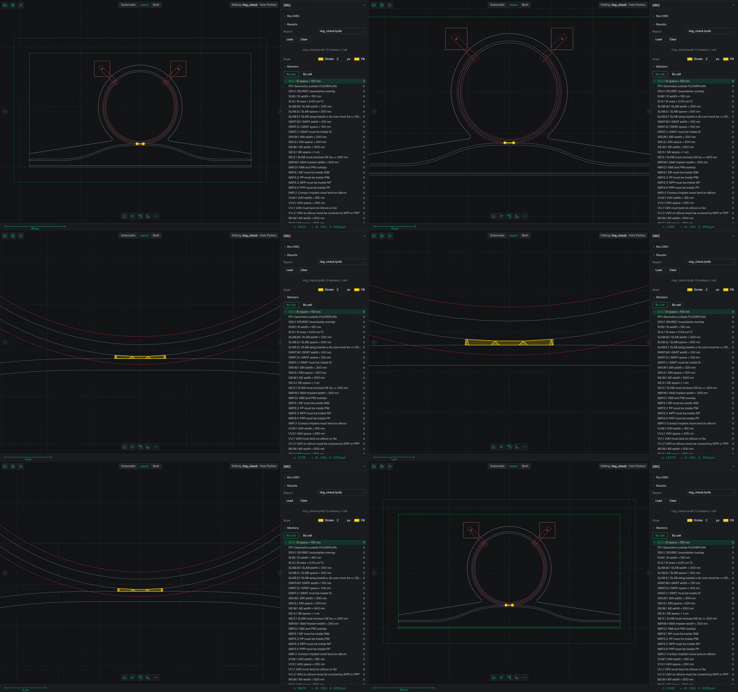
How do I run DRC checks?
Run the foundry rule deck on one cell or on the full chip. The violations show as markers on the layout and as a list in the local GUI. The checks run in KLayout 0.29.12 or newer, which you install separately, or in Calibre with a Photonic Canvas license. See Design Rule Check, Design Rule Check and Layout Verification.
How do I run LVS checks?
LVS extracts the netlist from the layout and compares it with the schematic. Optical connections come from the ports and the routes. Electrical connections come from the metal shapes and the vias. The report lists open nets, shorts and missing connections. LVS runs in KLayout 0.29.12 or newer, which you install separately. See Layout vs. Schematic (LVS) and Layout Verification.
How do I run Check Against Source?
Check Against Source runs in Cadence Virtuoso. The Cadence connector writes the PhotonForge layout and its schematic back to Virtuoso, where you run the check. Contact us to set up the Cadence connector.
Free and Paid
What is free, and what do I need to buy?
PhotonForge Community is free, with unlimited seats for engineers and AI agents. PhotonForge Enterprise, licensed as Photonic Canvas, adds foundry PDKs, EDA connectors, and version control and traceability in Photonic Canvas projects. The Community and Enterprise list on the front page shows what each edition includes. Tidy3D simulations use FlexCredits in both editions.
Is the layout tool free?
Yes. Layout, schematic, routing, DRC, LVS and the local GUI are in PhotonForge Community.
Can I modify parts of PhotonForge?
Yes, for your own use. You can change the Python parts of PhotonForge on your computer, and add your own PDKs, components, models and routes. You may not reverse engineer the compiled parts, include PhotonForge in other software that you distribute, open source or not, or sell software that is built on PhotonForge. See the Software License Agreement.
Local and Cloud
What parts of PhotonForge run in the cloud, and what parts run on my computer?
On your computer: the PhotonForge package, the local GUI, layout, schematic, routing, circuit simulation, DRC, LVS and Verilog-A export. In the Flexcompute cloud: Tidy3D simulations, and Photonic Canvas projects if you use them. PhotonForge also sends usage data to Flexcompute when it is imported and when a license check fails. Privacy and Usage Data lists what is sent and how to turn it off.
How do I use the GUI on-premises?
The local GUI runs on your computer and needs no server: open it from Python (see Getting Started). To keep Photonic Canvas projects on your own servers, use its on-premises deployment. Contact us for details.
How do I open the local GUI on a remote machine?
The local GUI listens only on the computer it runs on (127.0.0.1).
When Python runs on a remote machine, reach the GUI through a tunnel or a proxy:
SSH: run
ssh -L 8765:127.0.0.1:8765 user@remoteon your computer, then openhttp://localhost:8765. Use the port the GUI prints when it starts, or choose it withLiveViewer(port=8765).VS Code in the browser (code-server): open the address the GUI prints, under the proxy path such as
/proxy/8765/. No settings are needed.Other proxies, such as jupyter-server-proxy, a VS Code tunnel or a Codespace: give the GUI the host name the page is opened by, for example
LiveViewer(allowed_hosts=["jupyter.example.com"]).
To make the GUI reachable over the network instead, pass host="0.0.0.0".
Anything that can reach the port can then edit the design, so prefer a tunnel.
See live_viewer.LiveViewer for all options.
Where is my layout data stored?
In your own files: Python scripts, notebooks, GDS and OASIS files. If you use Photonic Canvas, the design is also stored in the Flexcompute cloud. Photonic Canvas also has an on-premises deployment, which stores the design on your own servers.
Where is my simulation data stored?
Tidy3D simulations run in the Flexcompute cloud, and their results stay in your Tidy3D account. PhotonForge also keeps a copy of the results on your computer, so it does not run the same simulation twice. Circuit simulations run on your computer.
Simulation and Measurement
Does PhotonForge include compact models based on measured data?
You can make a model from your measured data. Load measured S parameters from Touchstone files into a data model (Data Model), or fit a time-domain model to a measured response (Time-Domain Simulation of a Low-Pass Filter). In Photonic Canvas, attach the measurements to the design version that was fabricated, to compare them with the simulation.
Version Control, Traceability and Collaboration
How do I version control a project?
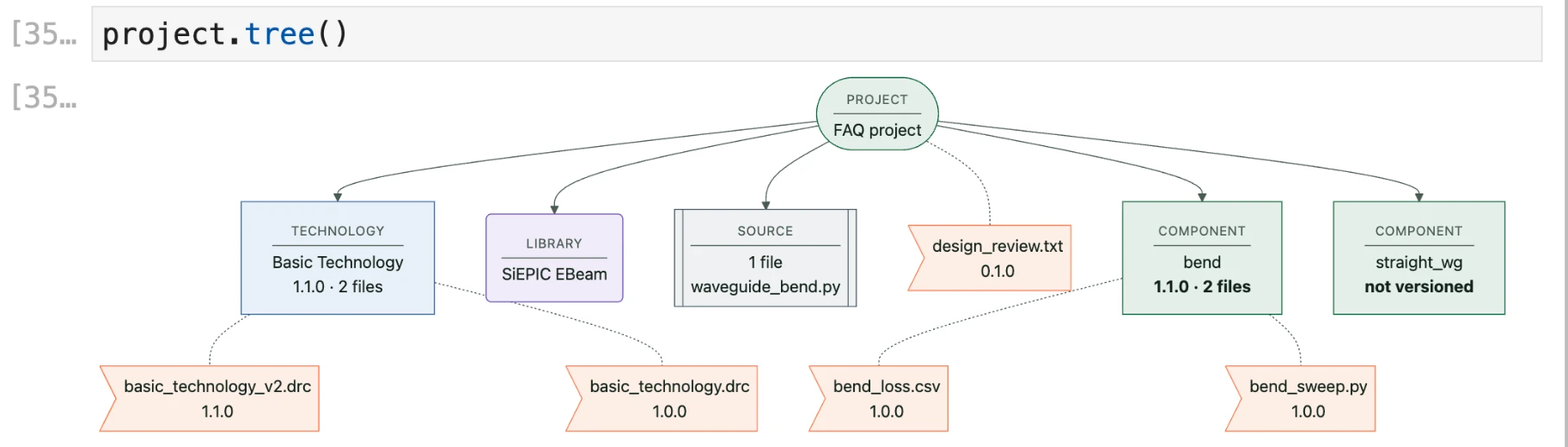
Use Photonic Canvas. A Photonic Canvas project stores the components, the PDK libraries and the code of a design. It keeps every edit. A version marks a release, for example the design that goes to tape-out. The Frequently Asked Questions: Photonic Canvas notebook answers 20 questions on projects, versions, sharing and traceability, with code.
Can I keep PDKs, simulation data and measurement data in one place?
Yes. Attach files to a component and a version: simulation scripts and results, DRC reports, masks and measurements. From any file, you can find the design and the PDK version it belongs to.
Python API
How to estimate the cost of an S matrix computation?
When using a Tidy3DModel, the cost can be estimated with the Tidy3DModel.estimate_cost function.
An example can be found in the Tidy3D Model guide.
How to change the layers of a component?
The function Component.remap_layers() can be used to efficiently remap the existing layers into new ones.
Can I use paths to create corrugated waveguides?
Yes, by parametrizing the width (and optionally the offset) of the path.
The parametrization uses an Expression to define the value and the derivative of the value for the with (or offset) along the path.
Here’s an example:
w0 = 0.5
dw = 0.1
scale = 50 * np.pi
width = pf.Expression(
    "u",
    [
        ("w", f"{w0} + {dw} * sin({scale} * u)"),
        ("dw_du", f"{dw * scale} * cos({scale} * u)"),
    ],
)

# Ring with both sides corrugated from the width expression
both_sides = pf.Path((0, 0), width(0)[0])
both_sides.arc(-90, 270, radius=5, width=width)

offset = pf.Expression(
    "u",
    [
        ("q", f"{-0.5 * dw} * sin({scale} * u)"),
        ("dq_du", f"{-0.5 * dw * scale} * cos({scale} * u)"),
    ],
)

# Single side corrugation by adjusting the central offset to compensate
# half of the width corrugation
one_side = pf.Path((15, 0), width(0)[0], offset(0)[0])
one_side.arc(-90, 270, radius=5, width=width, offset=offset)

How do I specify the number of vertices when a circle or a path is converted to a polygon?
You can set min_evals for Circle and Path objects to define the minimum number of points used when converting arcs in these shapes to polygonal lines. The actual number of points will be increased if necessary to ensure that config.tolerance is maintained.
How do I apply changes to a simulation object in a mode solver simulation?
You can use the updated_copy method to apply changes. This function creates a new object with the specified properties updated, without modifying the original object.
For example, the following line applies y-symmetry to a mode solver simulation:
mode_solver.simulation.updated_copy(symmetry=(0, -1, 0))
This same approach can be used to update other simulation object properties—such as grid spacing, boundary conditions, or source definitions—by calling updated_copy on the relevant part of the simulation and passing the desired new values as arguments.
How can I extract simulation data, such as field data, from Tidy3D?
You can extract simulation data from Tidy3D by accessing the Tidy3DModel.batch_data() method on your active model. This allows you to retrieve data associated with a specific simulation object. Once you have the simulation data, you can then plot a specific field component, such as "Ey", using the plot_field method, as demonstrated in the example below:
sim_data = c.active_model.batch_data(c, frequencies)
_ = sim_data["P0@0"].plot_field("field", "Ey", robust=False)
In the above example, c is the component and "field" is the name of a field monitor defined in the component’s model.
How can I simulate the S-matrix exclusively for a specific port?
To simulate the S-matrix exclusively for a specific port, you can pass the model_kwargs argument to the Component.s_matrix() call.
For example, to simulate the S-matrix using only port "P0" as the input:
s_matrix = c.s_matrix(freqs, model_kwargs={"inputs": ["P0"]})
How do I update a specific reference within a hierarchical component, such as its model?
You can update specific references within a hierarchical component by using a nested dictionary. The outer dictionary’s keys define the reference path starting from the top-level component, using a tuple of the form (reference name, reference index, ...).
The corresponding value is another dictionary that can include keys like "model_updates" (or other valid update types), which then maps variable names to their new values.
Here’s an illustrative example from the Switch Array notebook:
updates = {
    ("Unit Cell", 14, "Tunable MZI", 0, "Phase Shifter", 0): {
        "model_updates": {"n_complex": index(v_bar)}
    }
}

s_matrix = switch_array.s_matrix(
    pf.C_0 / wavelengths, model_kwargs={"updates": updates}
)
This mechanism allows fine-grained control over deeply nested components without modifying the original design.
How do I define port symmetries?
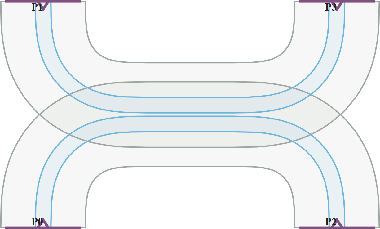
To define port symmetries, you should specify different port orderings that leave the S-matrix of the device unchanged. This is common for symmetric components like directional couplers.
Port symmetries are defined by listing alternative sequences of the output ports that correspond to equivalent physical configurations. Each tuple represents a reordering of the ports, where the ith element in the tuple is the port that replaces port Pi in the new configuration.
For example, consider a directional coupler with four ports labeled P0, P1, P2, and P3 in a rectangular layout:
Swapping
P0withP1andP2withP3corresponds to a reflection across the x-axis.Swapping
P0withP2andP1withP3corresponds to a reflection across the y-axis.Swapping
P0withP3andP1withP2corresponds to a 180° rotation (inversion symmetry).
These symmetries can be encoded as:
port_symmetries = [
    ("P1", "P0", "P3", "P2"),  # x-axis reflection
    ("P2", "P3", "P0", "P1"),  # y-axis reflection
    ("P3", "P2", "P1", "P0"),  # inversion symmetry
]
After defining symmetries, it is strongly recommended to validate them using the Tidy3DModel.test_port_symmetries() function. For faster validation, use a coarse grid and a single frequency point:
assert dc.active_model.test_port_symmetries(
    dc, frequencies=[pf.C_0 / 1.55], grid_spec=8
)
Is the order of ExtrusionSpec objects in a list important?
Yes, the order of ExtrusionSpec objects within a list is crucial, as it determines the sequence in which the extrusion operations are applied. This is particularly important for hierarchical extrusions or when one extrusion depends on the geometry created by a previous one.
In most cases, the order should follow the physical sequence of fabrication steps, ensuring that layers are built up in the correct order.
How can I modify a technology?
If the technology is parametric, you can update its parameters—such as layer thicknesses or medium definitions—either when first instantiating it or later by using the Technology.update() method.
You can also modify the structure of the technology by:
Adding or removing layers using
Technology.add_layer()andTechnology.remove_layer()Adding or removing ports using
Technology.add_port()andTechnology.remove_port()Defining or deleting connections between layers using
Technology.add_connection()andTechnology.remove_connection()Managing extrusion specifications using
Technology.insert_extrusion_spec()andTechnology.pop_extrusion_spec()
These capabilities give you full control over the technology stack to match your fabrication requirements.