
Y Splitter

This example demonstrates the use of PhotonForge to design and simulate a simple Y splitter based on [1]. We use the optimized geometry to create the splitter as a component with an FDTD model for performance verification. After creating the geometry and setting up the component ports and model, we’ll also demonstrate how to export it to the native PhotonForge format and to a GDSII file.
References
Yi Zhang, Shuyu Yang, Andy Eu-Jin Lim, Guo-Qiang Lo, Christophe Galland, Tom Baehr-Jones, and Michael Hochberg, “A compact and low loss Y-junction for submicron silicon waveguide,” Opt. Express 21, 1310-1316 (2013), doi: 10.1364/OE.21.001310
This example has an equivalent in the Tidy3D documentation: Waveguide Y junction.
[1]:
import numpy as np
import photonforge as pf
from matplotlib import pyplot as plt
Technology
The first step is to set up the default technology for this project. The original device is designed for a silicon-on-oxide (SOI) stack with a 220 nm thick device layer and a 500 nm wide waveguide. The basic_technology function defaults to those values, both for the stack and the "Strip" port specification.
[2]:
tech = pf.basic_technology()
pf.config.default_technology = tech
Here we can inspect the layer, port, and extrusion specifications defined in our default technology:
[3]:
tech.layers
[3]:
| Name | Layer | Description | Color | Pattern |
|---|---|---|---|---|
| WG_CLAD | (1, 0) | Waveguide clad | #9da6a218 | . |
| WG_CORE | (2, 0) | Waveguide core | #6db5dd18 | / |
| SLAB | (3, 0) | Slab region | #8851ad18 | : |
| TRENCH | (4, 0) | Deep-etched trench for chip…… facets | #535e5918 | + |
| METAL | (5, 0) | Metal layer | #b8a18b18 | \ |
[4]:
print("Port specifications:")
for name, spec in tech.ports.items():
    print(f"- {name}: {spec!r}")
Port specifications:
- CPW: PortSpec(description="CPW transmission line", width=18.7398, limits=(-6.46388, 10.4039), num_modes=1, added_solver_modes=0, polarization="", target_neff=4, default_radius=0, path_profiles={"gnd0": (6.8199, -6.20995, (5, 0)), "gnd1": (6.8199, 6.20995, (5, 0)), "signal": (3.6, 0, (5, 0))}, voltage_path=[(2.8, 1.97), (1.8, 1.97)], current_path=[(2.3, 2.72), (-2.3, 2.72), (-2.3, 1.22), (2.3, 1.22)], impedance=None)
- Rib: PortSpec(description="Rib waveguide", width=2.16, limits=(-1, 1.22), num_modes=1, added_solver_modes=0, polarization="", target_neff=4, default_radius=0, path_profiles=[(0.4, 0, (2, 0)), (2.4, 0, (3, 0)), (2.4, 0, (1, 0))])
- Strip: PortSpec(description="Strip waveguide", width=2.25, limits=(-1, 1.22), num_modes=1, added_solver_modes=0, polarization="", target_neff=4, default_radius=0, path_profiles=[(0.5, 0, (2, 0)), (2.5, 0, (1, 0))])
[5]:
print("Extrusion specifications:")
for i, spec in enumerate(tech.extrusion_specs):
    print(f"{i + 1}. {spec!r}")
Extrusion specifications:
1. ExtrusionSpec(mask_spec=MaskSpec(operand1=[], operand2=[], operation='+'), medium={"optical": cSi_Li1993_293K, "electrical": Medium(permittivity=12.3)}, limits=(-2e+07, 0), sidewall_angle=0, reference="top")
2. ExtrusionSpec(mask_spec=MaskSpec(operand1=[], operand2=[], operation='+'), medium={"optical": SiO2_Palik_LowLoss, "electrical": Medium(permittivity=4.2)}, limits=(-2, 1.72), sidewall_angle=0, reference=0)
3. ExtrusionSpec(mask_spec=MaskSpec((2, 0)), medium={"optical": cSi_Li1993_293K, "electrical": Medium(permittivity=12.3)}, limits=(0, 0.22), sidewall_angle=0, reference="top")
4. ExtrusionSpec(mask_spec=MaskSpec((3, 0)), medium={"optical": cSi_Li1993_293K, "electrical": Medium(permittivity=12.3)}, limits=(0, 0.07), sidewall_angle=0, reference="top")
5. ExtrusionSpec(mask_spec=MaskSpec((5, 0)), medium={"optical": Cu_JohnsonChristy1972, "electrical": PEC}, limits=(1.72, 2.22), sidewall_angle=0, reference="top")
6. ExtrusionSpec(mask_spec=MaskSpec((4, 0)), medium={"optical": Medium(), "electrical": Medium()}, limits=(-2e+07, 2e+07), sidewall_angle=0, reference="top")
Geometry
After the technology setup, we create the geometry, starting with the main polygon, as described in the reference work.
[6]:
# Values from the optimized Y splitter
w = np.array((0.5, 0.5, 0.6, 0.7, 0.9, 1.26, 1.4, 1.4, 1.4, 1.4, 1.31, 1.2, 1.2))
length = 2.0
y_out = 0.35

vertices = np.vstack((np.linspace(0, length, len(w)), -0.5 * w)).T
y_polygon = pf.Polygon(np.vstack((vertices, vertices[::-1] * np.array((1, -1)))))

y_polygon
[6]:

The output ports for this junction are very close to each other, which couples the modes from the 2 output waveguides. S-parameter calculations assume that ports are independent, so there can be no coupling between modes from different ports, which means that we have 2 options:
Create a new port specification that includes both output waveguides and supports both modes, or
Physically separate the outputs so that we can use 2 independent strip waveguide ports.
The first solution means that components connecting to our splitter output would also have to use our new bimodal port, which is less convenient than the second solution.
Just for completeness, this is what the bimodal port specification would look like:
[7]:
port_spec = pf.config.default_technology.ports["Strip"]

bimodal_clad_margin = 2 * (w[-1] + 2)
bimodal_port = pf.PortSpec(
    "Output test",
    width=0.9 * bimodal_clad_margin,
    limits=port_spec.limits,
    num_modes=2 * port_spec.num_modes,
    target_neff=port_spec.target_neff,
    path_profiles={
        (bimodal_clad_margin, 0, "WG_CLAD"),
        (0.5, y_out, "WG_CORE"),
        (0.5, -y_out, "WG_CORE"),
    },
)
We can inspect the port modes and verify that they are, indeed, coupled: the 2 single waveguide modes are split in a pair with different effective indices. If the modes were uncoupled, they would have the same effective index as the isolated waveguide.
[8]:
mode_solver = pf.port_modes(bimodal_port, [pf.C_0 / 1.55])

_, ax = plt.subplots(1, 2, figsize=(10, 2), tight_layout=True)
mode_solver.plot_field("Ey", mode_index=0, robust=False, ax=ax[0])
mode_solver.plot_field("Ey", mode_index=1, robust=False, ax=ax[1])

mode_solver.data.to_dataframe()
Uploading task 'Mode-ModeSolver…'
Starting task 'Mode-ModeSolver': https://tidy3d.simulation.cloud/workbench?taskId=mo-abb11560-581b-4682-855d-234a183c8b96
Downloading data from 'Mode-ModeSolver'…
Progress: 100%
[8]:
| wavelength | n eff | k eff | loss (dB/cm) | TE (Ey) fraction | wg TE fraction | wg TM fraction | mode area | ||
|---|---|---|---|---|---|---|---|---|---|
| f | mode_index | ||||||||
| 1.934145e+14 | 0 | 1.55 | 2.450737 | 0.0 | 0.0 | 0.983193 | 0.798166 | 0.814268 | 0.391730 |
| 1 | 1.55 | 2.429558 | 0.0 | 0.0 | 0.984097 | 0.735946 | 0.819695 | 0.369463 |
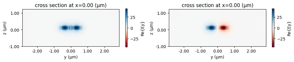
We will go ahead with the second solution by splitting the outputs with conventional S bends. We can use the Path.s_bend function to build the core waveguide geometry. The S bend offset is based on the port width to ensure the outputs have no overlap, and its length is chosen as a somewhat safe value to limit bend losses, but it can be fine-tuned reduce the component size if desired.
[9]:
clad_width, _ = port_spec.path_profile_for("WG_CLAD")
core_width, _ = port_spec.path_profile_for("WG_CORE")
clad_margin = (clad_width - core_width) / 2

s_offset = clad_width / 2 - clad_margin / 2 - y_out
s_length = 5 * s_offset
s_bend1 = pf.Path((length, y_out), core_width).s_bend((s_length, s_offset), relative=True)
s_bend2 = pf.Path((length, -y_out), core_width).s_bend((s_length, -s_offset), relative=True)

y_splitter = pf.Component("Y_SPLITTER")
y_splitter.add("WG_CORE", y_polygon, s_bend1, s_bend2)
[9]:

The basic technology includes a clad region by default in all port specifications. We can add a clad region to the main polygon manually, by specifying it ourselves based on the polygons coordinates, or using the envolope or offset functions. The envelope is similar to the offset, but it is based on the convex hull of the structures, resulting in a convex polygon.
We use the envelope function making sure to limit the envelope in the x direction to have our ports at the boundaries of the component. This is not strictly required, but can be helpful when connecting other components later or when using port auto-detection.
If we want to preserve the size of the original clad, we can get the widths for the strip waveguide core and cladding sections from its path profiles. We’re ignoring the offsets in the profiles here because we know, from our earlier inspection, that they are 0.
[10]:
clad = pf.envelope(
    y_splitter.get_structures("WG_CORE"), clad_margin, trim_x_min=True, trim_x_max=True
)
y_splitter.add("WG_CLAD", clad)
[10]:

Ports
We can use auto-detection to add the device ports. That only works because we’ve added the cladding edges required by the Strip specification.
[11]:
candidates = y_splitter.detect_ports(["Strip"])
candidates
[11]:
[Port(center=(0, 0), input_direction=0, spec=PortSpec(description="Strip waveguide", width=2.25, limits=(-1, 1.22), num_modes=1, added_solver_modes=0, polarization="", target_neff=4, default_radius=0, path_profiles=[(0.5, 0, (2, 0)), (2.5, 0, (1, 0))]), extended=True, inverted=False, bend_radius=0),
 Port(center=(4, -0.75), input_direction=180, spec=PortSpec(description="Strip waveguide", width=2.25, limits=(-1, 1.22), num_modes=1, added_solver_modes=0, polarization="", target_neff=4, default_radius=0, path_profiles=[(0.5, 0, (2, 0)), (2.5, 0, (1, 0))]), extended=True, inverted=False, bend_radius=0),
 Port(center=(4, 0.75), input_direction=180, spec=PortSpec(description="Strip waveguide", width=2.25, limits=(-1, 1.22), num_modes=1, added_solver_modes=0, polarization="", target_neff=4, default_radius=0, path_profiles=[(0.5, 0, (2, 0)), (2.5, 0, (1, 0))]), extended=True, inverted=False, bend_radius=0)]
Once we confirm the ports are correctly detected, we add them:
[12]:
y_splitter.add_port(candidates)
y_splitter
[12]:

Model
We add a Tidy3DModel to the component to simulate it using FDTD. Because of the device symmetry, we don’t need to excite both ports P1 and P2: the parameters extracted from the excitation of P2 can be computed from the excitation of P1, because is \(S_{22} = S_{11}\) and \(S_{20} = S_{10}\) (and reciprocals). We indicate that the S matrix remains the same if we exchange P1 and P2 by adding the tuple ("P0", "P2", "P1") to the list of
port_symmetries, in which we perform the exchange with respect to the sorted port list P0, P1, P2.
If necessary, we can test the symmetry using the test_port_symmetries method, as demonstrated in the Tidy3D model guide.
[13]:
tidy3d_model = pf.Tidy3DModel(port_symmetries=[("P0", "P2", "P1")])
y_splitter.add_model(tidy3d_model, "Tidy3D")

y_splitter.active_model
[13]:
Tidy3DModel(run_time=None, medium=None, symmetry=(0, 0, 0), boundary_spec=None, monitors=(), structures=(), grid_spec=None, shutoff=None, subpixel=None, courant=None, port_symmetries=[('P0', 'P2', 'P1')], bounds=((None, None, None), (None, None, None)), source_gap=None, simulation_updates=None, autograd_config=None, verbose=True)
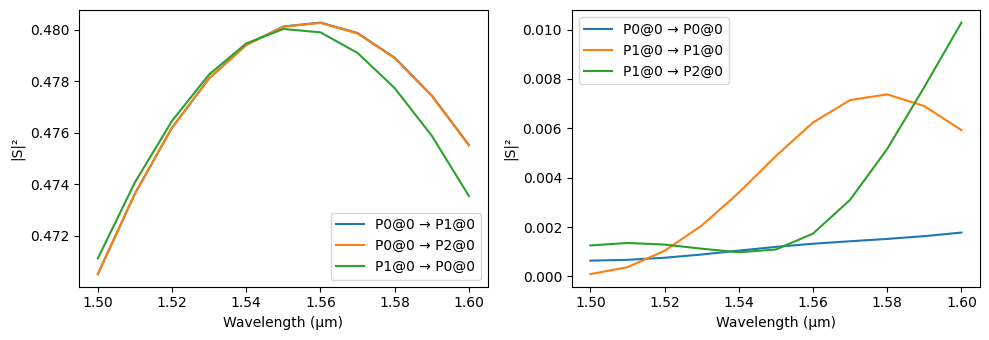
S parameters
With the model and ports set up, calculating the S parameters is a simple call to the s_matrix function with the desired frequencies:
[14]:
lda = np.linspace(1.5, 1.6, 11)
freqs = pf.C_0 / lda

s_matrix = y_splitter.s_matrix(freqs)
Uploading task 'P0@0…'
Uploading task 'P1@0…'
Starting task 'P1@0': https://tidy3d.simulation.cloud/workbench?taskId=fdve-b92798f0-d183-4406-9c52-c1297dce3c7d
Starting task 'P0@0': https://tidy3d.simulation.cloud/workbench?taskId=fdve-dd8353a9-0b00-4cd7-b820-3769b37e788b
Downloading data from 'P1@0'…
Downloading data from 'P0@0'…
Progress: 100%
The S matrix can be sparse, so it stores the elements as a dictionary indexed by tuples of origin and destination ports. Because each port can support multiple modes, the mode index is appended to the port name in the S dictionary keys after the @ character:
[15]:
print(s_matrix.elements.keys())
dict_keys([('P0@0', 'P0@0'), ('P0@0', 'P1@0'), ('P0@0', 'P2@0'), ('P1@0', 'P0@0'), ('P1@0', 'P1@0'), ('P1@0', 'P2@0'), ('P2@0', 'P0@0'), ('P2@0', 'P1@0'), ('P2@0', 'P2@0')])
For example, the element \(S_{10}\), representing the transmission coefficient from P0 to P1 can be retrieved as:
[16]:
s_matrix[("P0@0", "P1@0")]
[16]:
array([ 0.52513759+0.43961869j,  0.66775268+0.16283107j,
        0.67379311-0.14556554j,  0.54628725-0.42294031j,
        0.3145028 -0.61630962j,  0.02605632-0.69197166j,
       -0.26372263-0.64033209j, -0.50276007-0.47561737j,
       -0.6513834 -0.23121003j, -0.68823687+0.04803074j,
       -0.61219012+0.31455727j])
The utility function plot_s_matrix can be used to quickly plot the S parameters. We use only ports P0 and P1 as input ports for plotting, because the input from P2 is the same as from P1 (according to our symmetry settings).
[17]:
fig, ax = pf.plot_s_matrix(s_matrix, input_ports=["P0", "P1"])
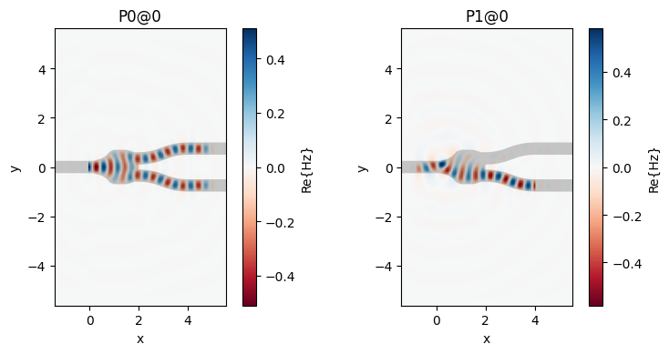
Inspecting the Fields
It is possible to obtain the field distributions in the device by adding a field monitor to the Tidy3D model. We have to re-run the simulation to use the new model and then get the simulation data for plotting.
[18]:
import tidy3d as td

tidy3d_model_with_monitor = pf.Tidy3DModel(
    port_symmetries=[("P1", "P2", {"P0": "P0", "P2": "P1"})],
    monitors=[
        td.FieldMonitor(
            name="field",
            center=(0, 0, 0.11),
            size=(td.inf, td.inf, 0),
            freqs=[freqs[freqs.size // 2]],
        )
    ],
)
y_splitter.add_model(tidy3d_model_with_monitor, "Tidy3DModel with monitor")

s_matrix = y_splitter.s_matrix(freqs)
Uploading task 'P0@0…'
Uploading task 'P1@0…'
Starting task 'P1@0': https://tidy3d.simulation.cloud/workbench?taskId=fdve-402e34fa-6a1d-48e2-9d53-cfa0655cd15e
Starting task 'P0@0': https://tidy3d.simulation.cloud/workbench?taskId=fdve-f25ebd4f-2ade-4452-b86b-7a613e707509
Downloading data from 'P1@0'…
Downloading data from 'P0@0'…
Progress: 100%
The simulation data is stored by the model, so we need to call batch_data on the model, passing the splitter as an argument. The returned value is a BatchData object, so we can inspect the simulations it stored from its task_ids dictionary:
[19]:
sim_data = tidy3d_model_with_monitor.batch_data(y_splitter, freqs)
sim_data.task_ids
Progress: 100%
07:26:27 -03 Loading simulation from local cache. View cached task using web UI
             at
             'https://tidy3d.simulation.cloud/workbench?taskId=fdve-f25ebd4f-2ad
             e-4452-b86b-7a613e707509'.
             Loading simulation from local cache. View cached task using web UI
             at
             'https://tidy3d.simulation.cloud/workbench?taskId=fdve-402e34fa-6a1
             d-48e2-9d53-cfa0655cd15e'.
[19]:
{'P0@0': 'fdve-f25ebd4f-2ade-4452-b86b-7a613e707509',
 'P1@0': 'fdve-402e34fa-6a1d-48e2-9d53-cfa0655cd15e'}
[20]:
_, ax = plt.subplots(1, 2, figsize=(8, 4), tight_layout=True)

for i, name in enumerate(sorted(sim_data.task_ids)):
    sim_data[name].plot_field("field", "Hz", robust=False, ax=ax[i])
    ax[i].set_title(name)
Saving and Exporting
The final component can be saved to a native PhotonForge project file (.phf), which stores all information associated with the component (including parametric arguments, for example). This file is also compatible with our web UI, if we want to continue using the splitter via GUI.
Note that the function write_phf can store several components (or technologies) in a single file, and it includes all dependencies automatically. For example, when we store the y_splitter component, the s_bend will also be included, as well as the basic technology they use.
[21]:
pf.write_phf("Y_Splitter.phf", y_splitter)
Just for demonstration, we can load the created file to check its contents:
[22]:
contents = pf.load_phf("Y_Splitter.phf")

print("Loaded components:", len(contents["components"]))
for c in contents["components"]:
    print(
        f"- {c} (structures: {len(c.structures)}; references: {len(c.references)}; ports: {len(c.ports)}; models: {len(c.models)})"
    )

print("Loaded technologies:", len(contents["technologies"]))
for t in contents["technologies"]:
    print(f"- {t}")
Loaded components: 1
- Component "Y_SPLITTER" (structures: 2; references: 0; ports: 3; models: 2)
Loaded technologies: 0
Although we don’t see the S bend or the basic technology in the contents, they are stored within the loaded splitter. By default, load_phf will only list the explicitly saved items the returned dictionary. We can change that by setting only_explicit to False:
[23]:
contents = pf.load_phf("Y_Splitter.phf", only_explicit=False)

print("Loaded components:", len(contents["components"]))
for c in contents["components"]:
    print(
        f"- {c} (structures: {len(c.structures)}; references: {len(c.references)}; ports: {len(c.ports)}; models: {len(c.models)})"
    )

print("Loaded technologies:", len(contents["technologies"]))
for t in contents["technologies"]:
    print(f"- {t}")
Loaded components: 1
- Component "Y_SPLITTER" (structures: 2; references: 0; ports: 3; models: 2)
Loaded technologies: 1
- Basic Technology 1.5.0
Finally, we can also export the device to a GDSII or an OASIS file (methods write_gds and write_oas can be used to quickly export a single component, and function write_layout for multiple components in a single file). Those interchange formats do not store all information available in the component, such as technology specifications or modes, so loading back from them will not result in the original component.
[24]:
y_splitter.write_gds("Y_Splitter.gds")

contents = pf.load_layout("Y_Splitter.gds")

print("Loaded components:", len(contents))
for _, c in contents.items():
    print(
        f"- {c} (structures: {len(c.structures)}; references: {len(c.references)}; ports: {len(c.ports)}; models: {len(c.models)})"
    )
Loaded components: 1
- Component "Y_SPLITTER" (structures: 2; references: 0; ports: 0; models: 0)