PhotonForge 2.0
PhotonForge 2.0 is an end-to-end design automation platform for photonic integrated circuits. It takes a chip from the PDK to tape-out and test: schematic, layout and routing, device and circuit simulation, design-rule checks, and version control of the design and its data. Engineers and AI agents design the chip together, with the same Python API and the same local GUI.
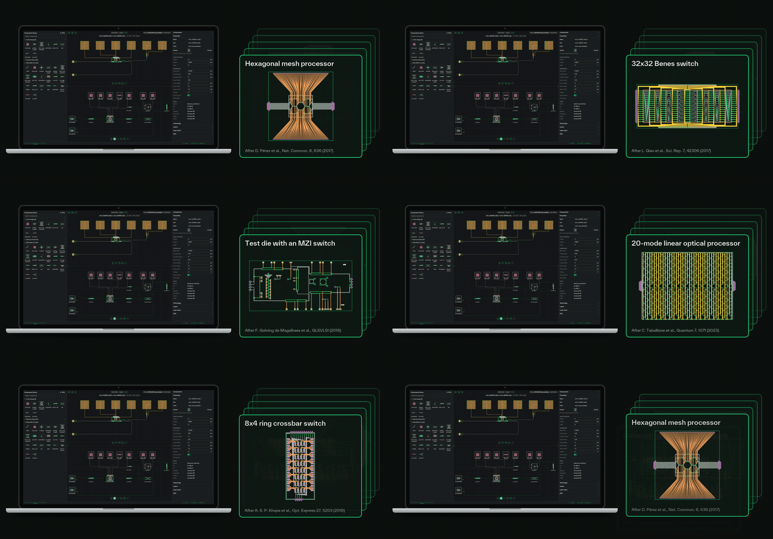
Free to start, in one command
PhotonForge 2.0 Community is free for research and commercial use, with unlimited seats for engineers and AI agents.
pip install photonforge
Layout, schematic, routing, DRC and circuit simulation run on your computer. A free Tidy3D account adds device simulation in the cloud. Next, build your first circuit in the local GUI with the Quick Start.
PhotonForge Enterprise, licensed as Photonic Canvas, adds foundry PDKs, EDA connectors, and version control and traceability for teams that take designs to production (see Community and Enterprise).
From Schematic to Tape-Out on One Chip
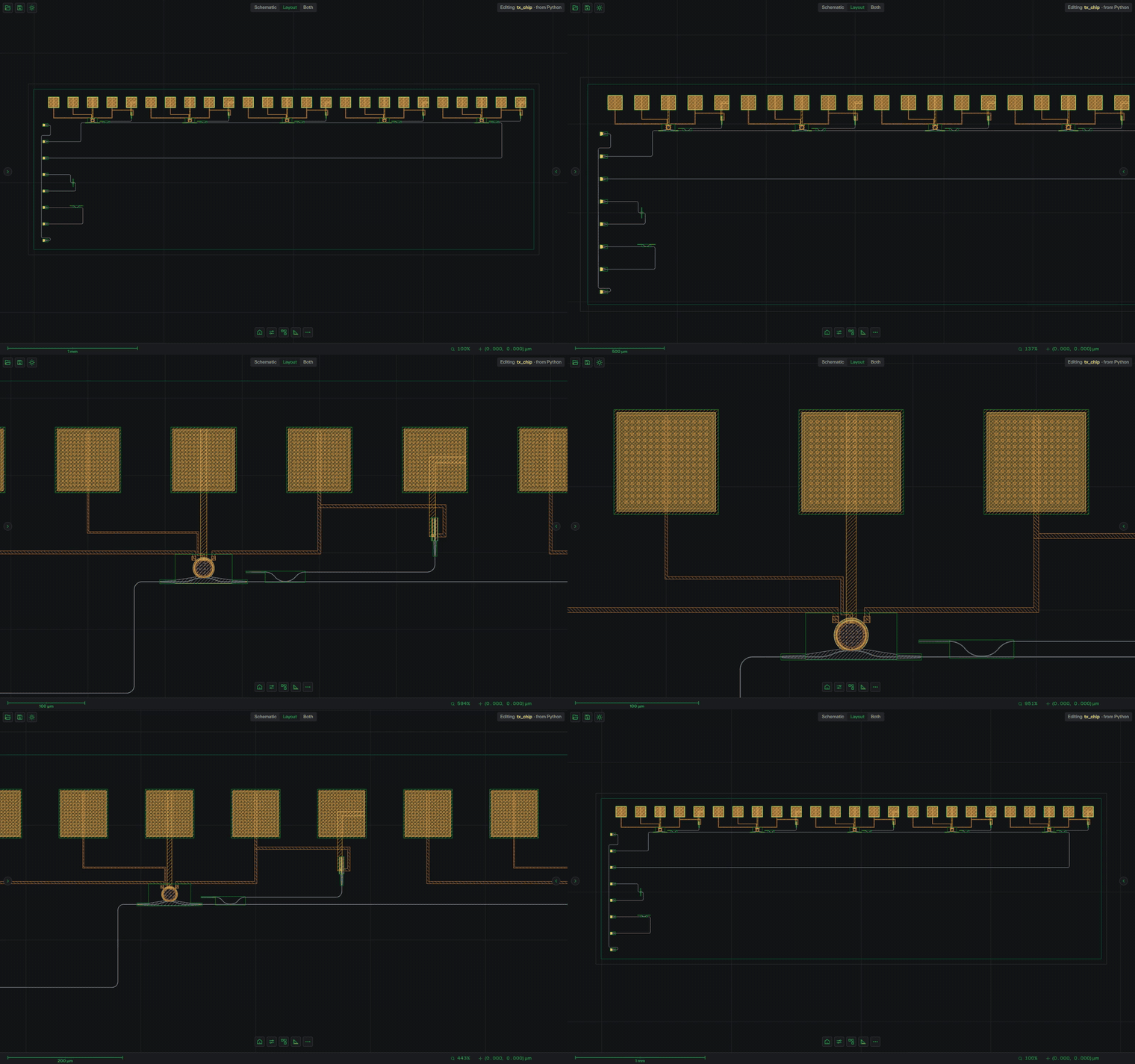
The steps below follow one chip through the design flow: a five-channel ring-modulator transmitter for a datacom link. The chip uses SiPhoPDK, a demo silicon photonics PDK. Each step shows what PhotonForge does and links to the guides and examples.
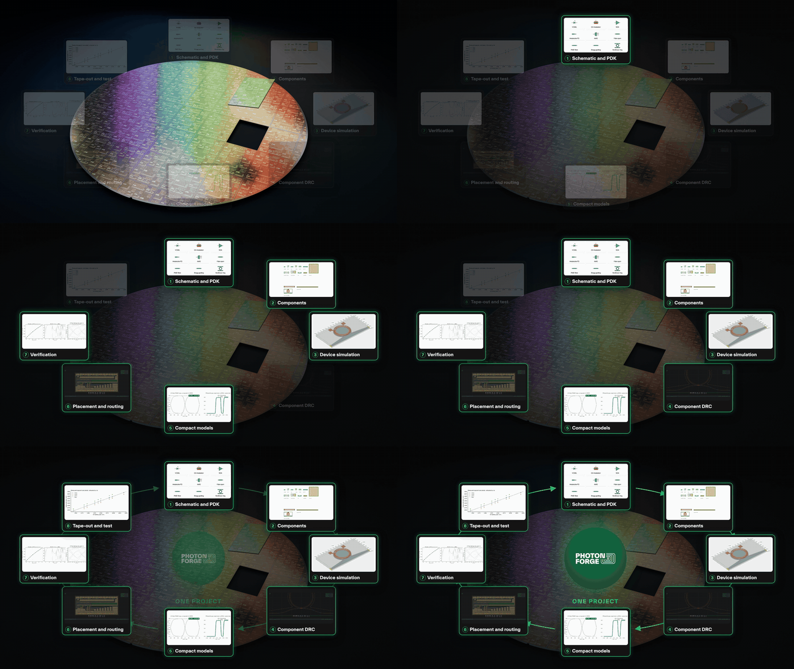
1. Schematic and PDK
A PDK in PhotonForge holds the layer stack, the waveguide cross sections, the cells and their models.
Install an open PDK with pip, or load your foundry PDK.
Then draw the circuit as a schematic in the local GUI, with the PDK cells in the library panel, or write it as a netlist in Python.
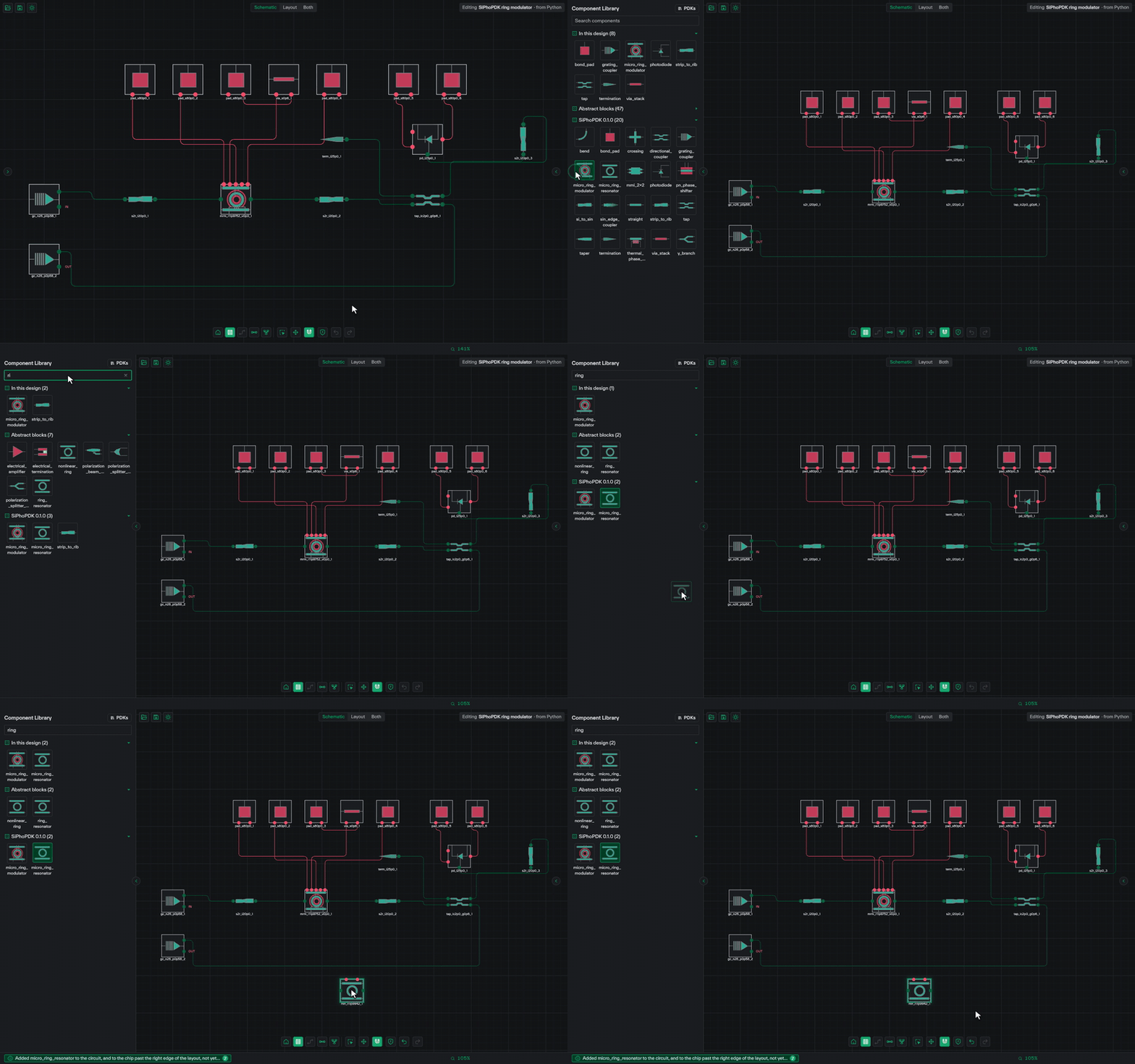
Learn more: Technology, PDK Components, Technology and PDK Setup
2. Components
Each cell is a parametric component: a Python function that draws the layout from its parameters and attaches a simulation model. Change a parameter, and the layout and the model change with it. The same component shows as a symbol in the schematic and as geometry in the layout. You can also draw a cell in the layout tool you already use and import it as a GDS or OASIS file, or load it from Cadence Virtuoso through its OpenAccess database.
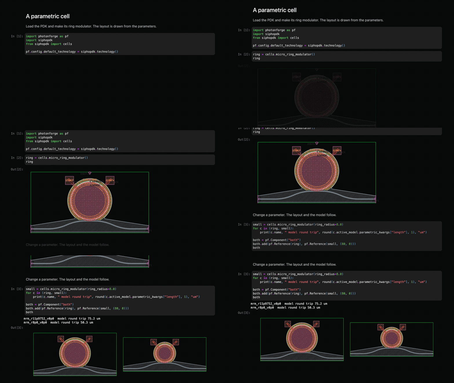
Learn more: Custom Parametric Components, Parametric Component Library, Microring Modulator: PCell with Attached Model
3. Device Simulation
Send a component to Tidy3D directly from its layout. PhotonForge builds the 3D structures from the PDK layer stack and places the ports. FDTD, EME or the mode solver then calculates the S parameters. The same structures go to the Tidy3D charge, heat and RF solvers.
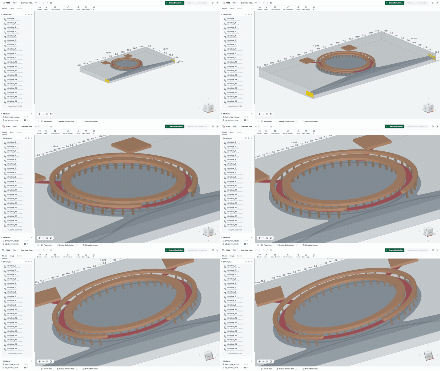

Learn more: Tidy3D Model, MMI 3 dB Coupler with EME, 3D doping extrusion from a 2D carrier profile
4. Component DRC
Check each cell against the foundry design rules before you place it on the chip. Run DRC from the local GUI or from Python. Each violation shows in a list and as a marker on the layout.
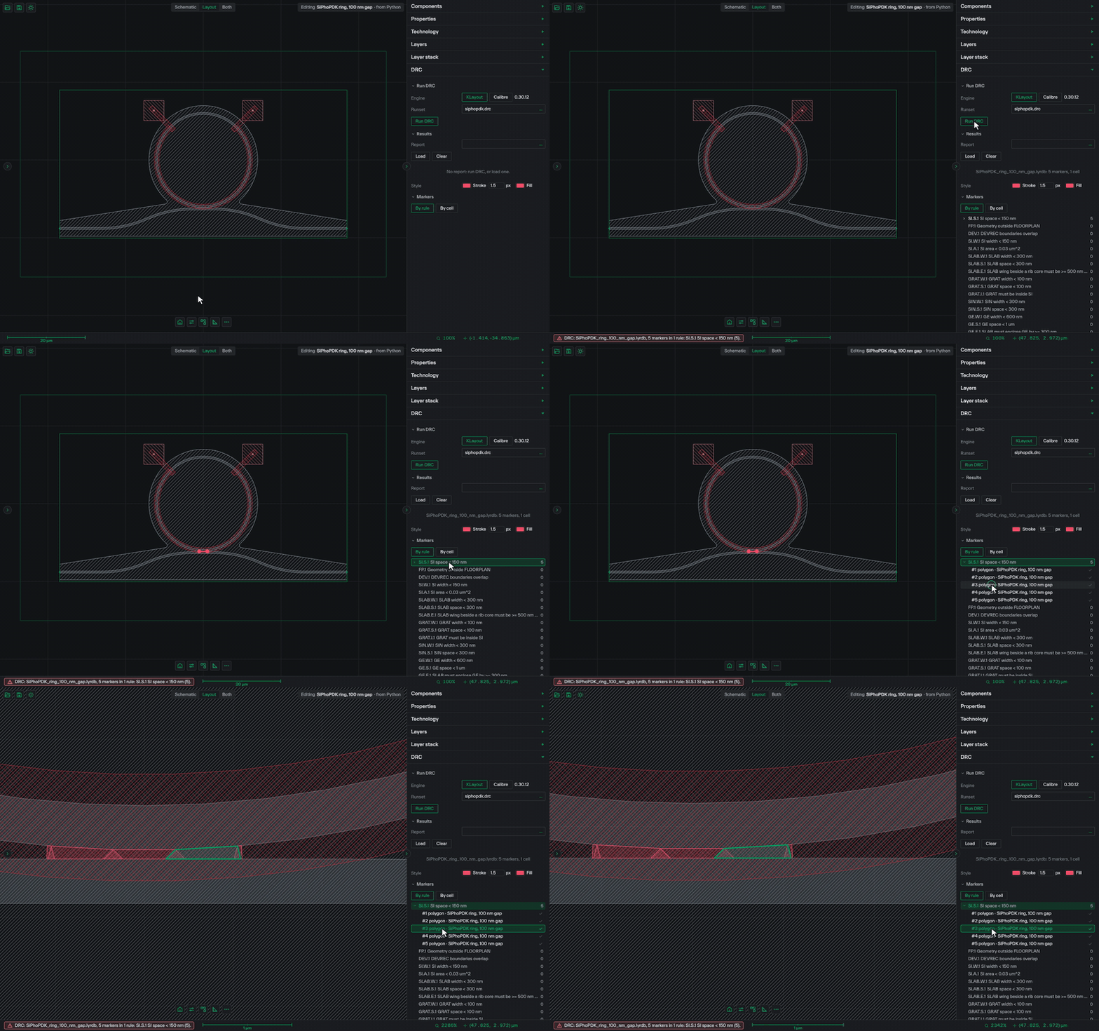
Learn more: Design Rule Check, Design Rule Check
5. Compact Models
For circuit simulation, each component carries a compact model. A model comes from an analytic formula, from Tidy3D results, or from measured data. Time-domain models include lasers, modulators, rings with nonlinear effects, optical amplifiers and photodiodes. Export a model to Verilog-A to run it in a SPICE simulator next to the electronics.
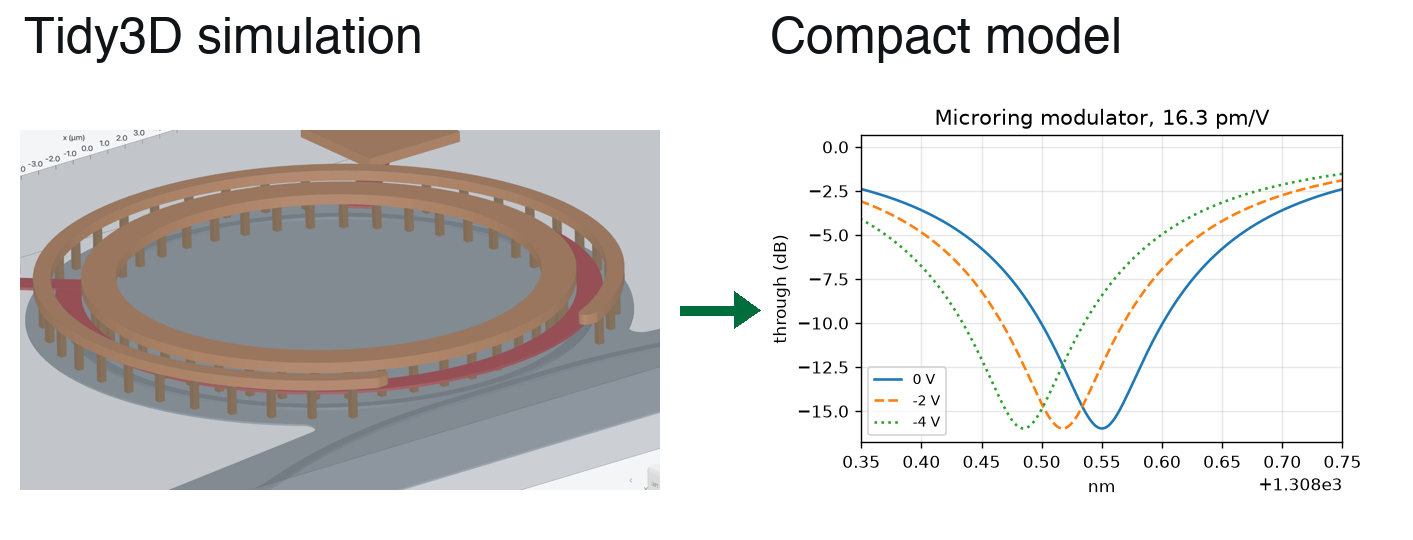
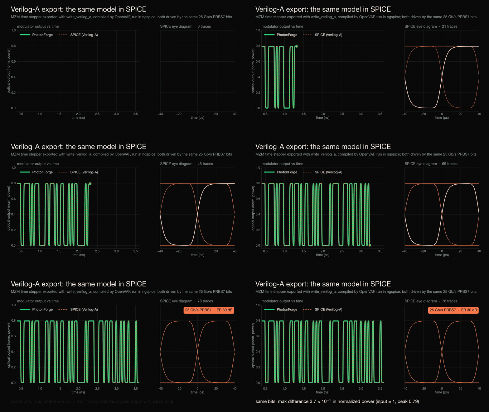
Learn more: Compact Models, Time Domain Models, Data Model, Custom Model
6. Placement and Routing
In the local GUI, Place puts the cells on the chip where the schematic has them, and Route draws the waveguides.
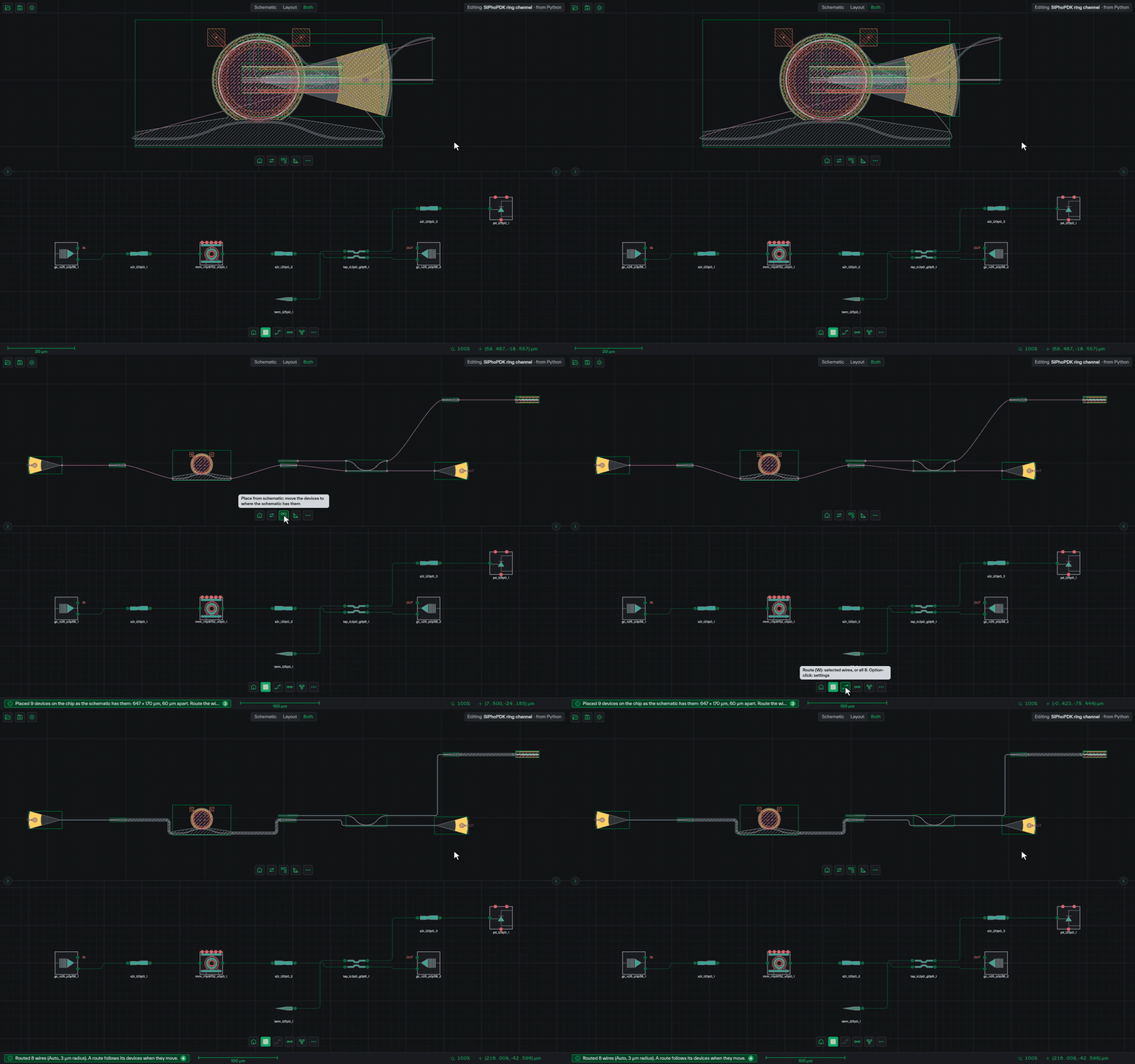
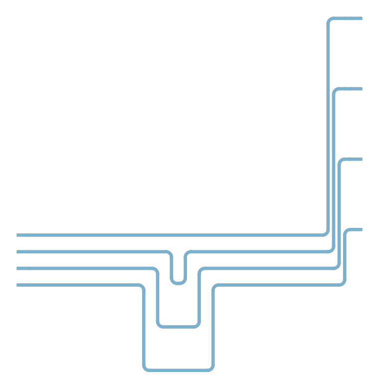
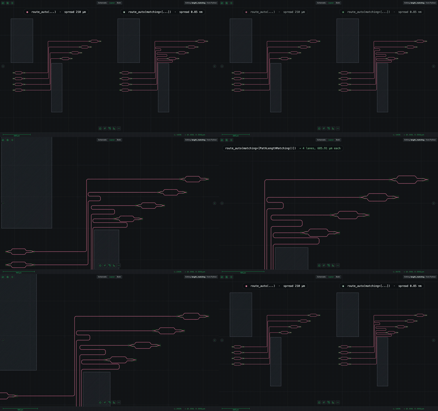
The autorouter routes all optical nets in one call. It avoids obstacles, adds waveguide crossings where it needs them, and can make the path lengths equal.
This script routes four waveguides to a fiber array with equal path lengths:
import photonforge as pf

pf.config.default_technology = pf.basic_technology()

chip = pf.Component("FANOUT")
wg = pf.parametric.straight(port_spec="Strip", length=20)

# Four waveguides 30 µm apart, and four fiber-array inputs 127 µm apart
devices = [chip.add_reference(wg).translate((0, 30 * i)) for i in range(4)]
fibers = [chip.add_reference(wg).translate((600, 100 + 127 * i)) for i in range(4)]

# Route the four nets in one call, with equal path lengths
routes = pf.parametric.route_auto(
    port1=[(d, "P1") for d in devices],
    port2=[(f, "P0") for f in fibers],
    radius=10,
    matching=[pf.PathLengthMatching()],
)
chip.add_reference(routes)
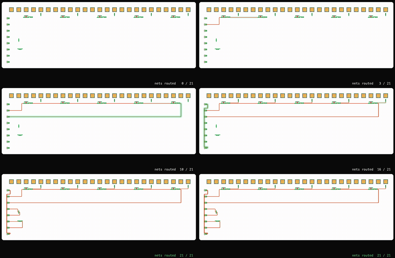
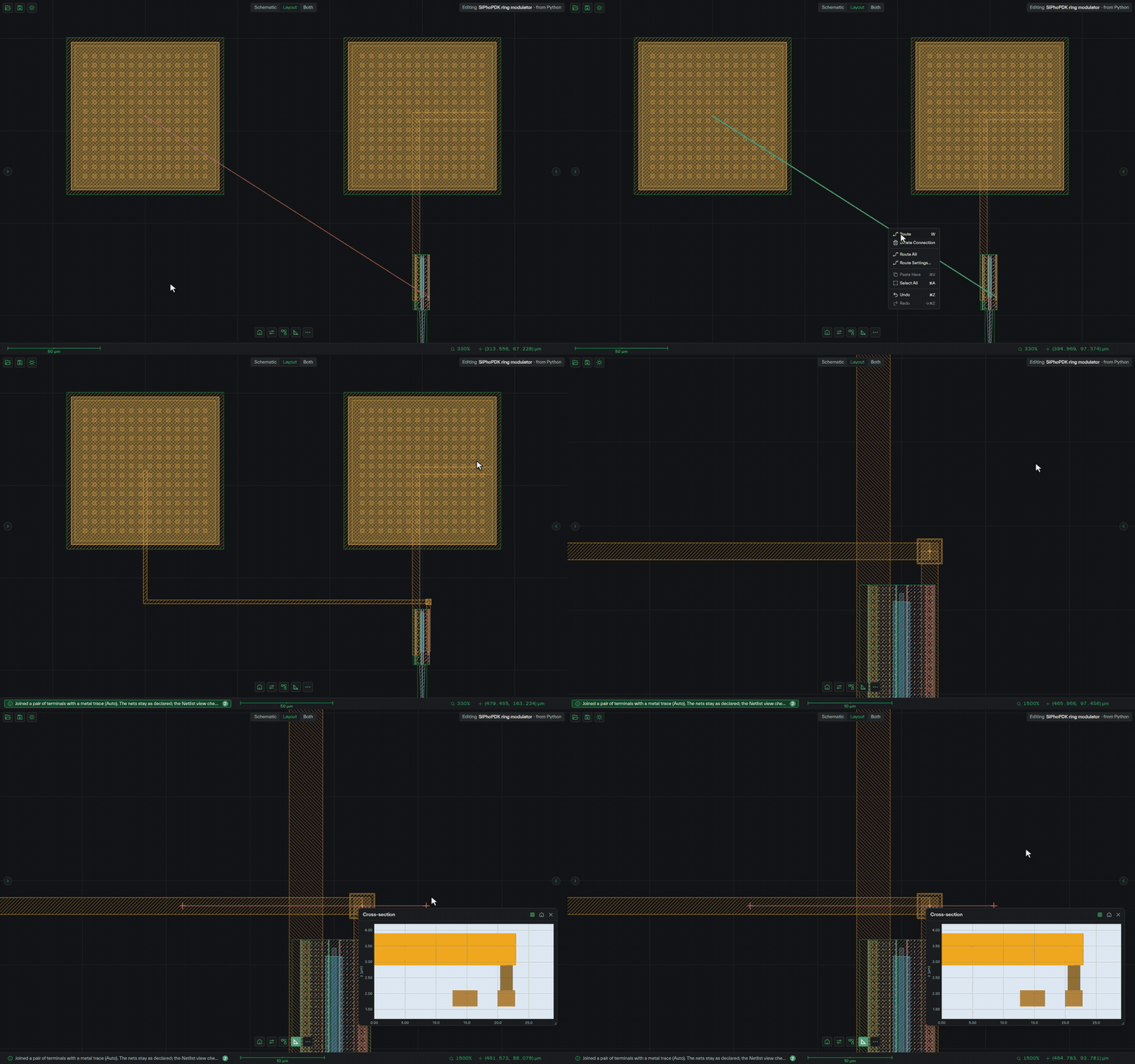
Electrical traces go to the pads on the metal layers of the PDK, with a via where a trace changes layer.
Learn more: Auto Routing, Routing and Connections, Chip Layout
7. Verification
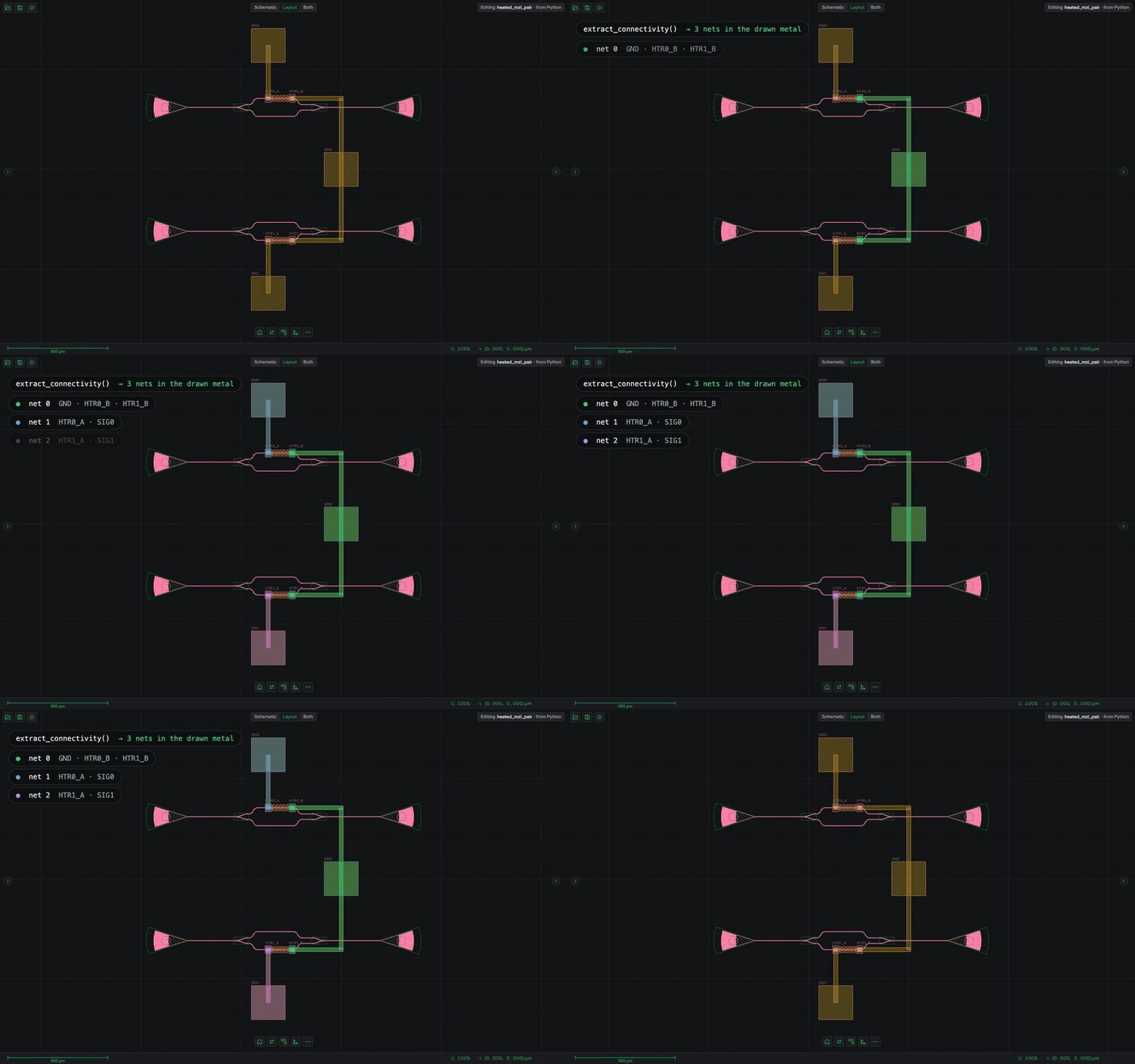
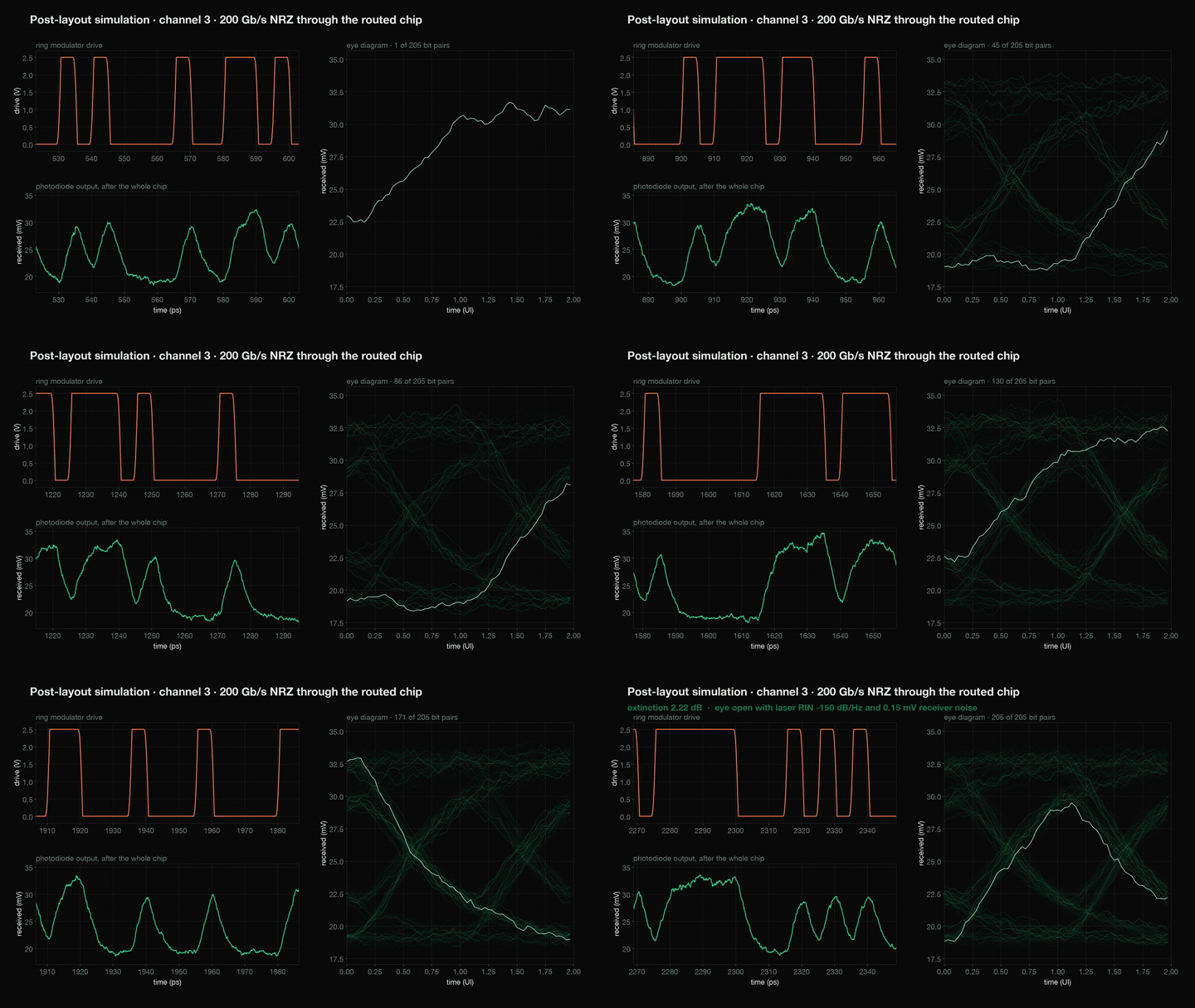
Run DRC on the full chip with the foundry rule deck. LVS extracts the optical and electrical netlist from the layout and compares it with the schematic. Post-layout simulation then runs the circuit as it is drawn, with every route, for example to get the eye diagram of one modulator channel.
Cadence Virtuoso users load the PDK cells into PhotonForge, run Tidy3D multiphysics simulations on them, and write the finished chip back to Virtuoso, where Check Against Source compares it with the schematic. The design stays in their existing EDA flow. Contact us to set up the Cadence connector.
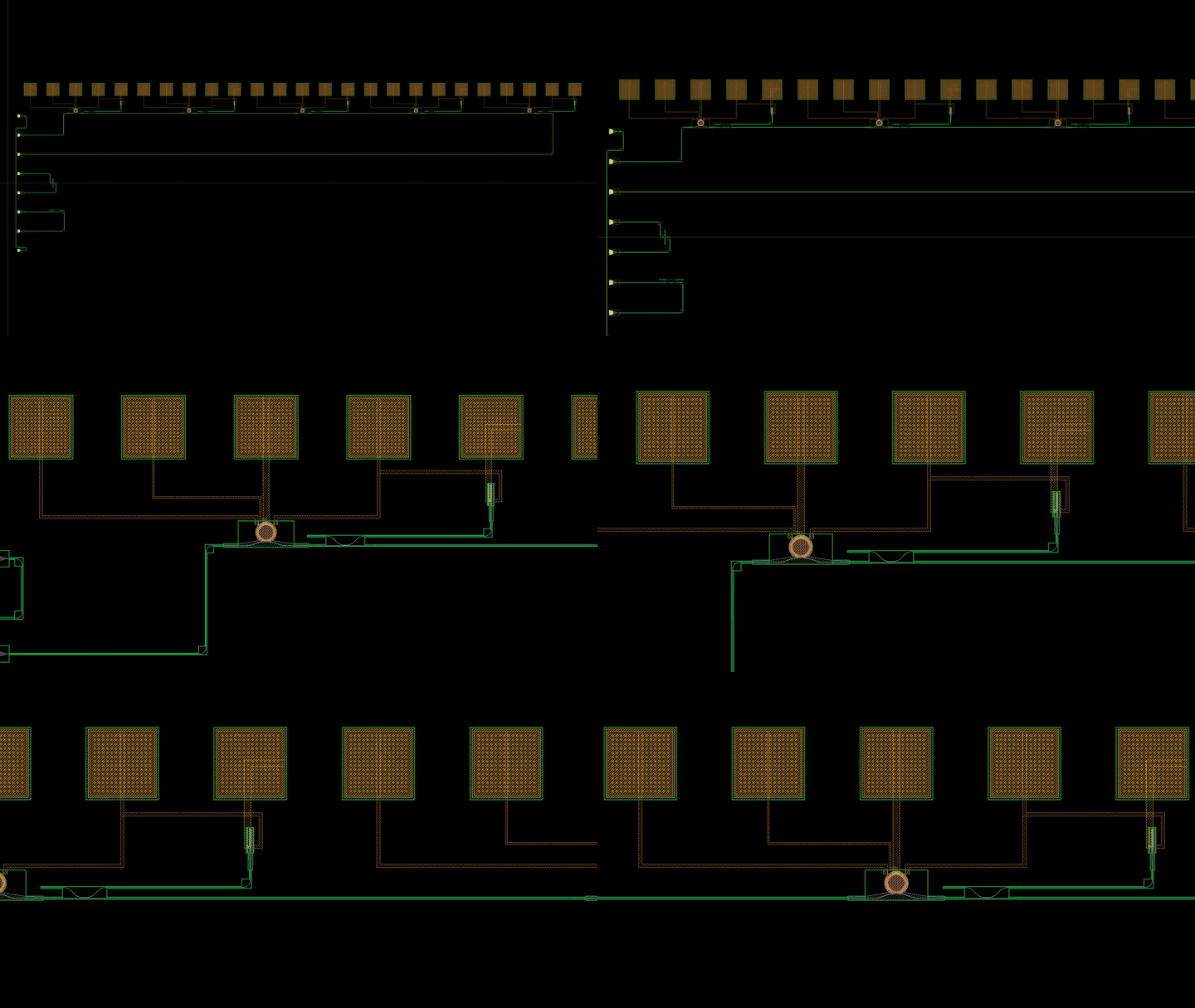
Learn more: Design Rule Check, Layout vs. Schematic (LVS), Chip Simulation
8. Tape-Out and Test with Photonic Canvas
A Photonic Canvas project keeps the design, the PDK version, the simulation results and the measured data together. Release a version for tape-out and attach the mask, the DRC report and, later, the measurements to it. A measured die then traces back to the exact design that made it.
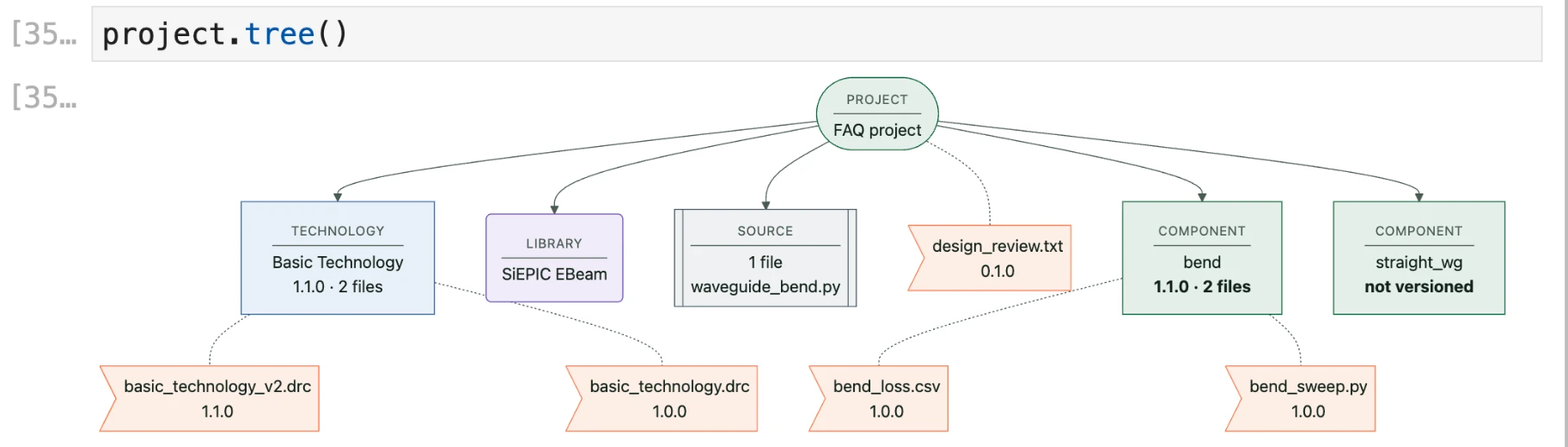
Learn more: Frequently Asked Questions: Photonic Canvas, Photonic Design Automation
Ways to Work
Python
Every step is a Python call, so a notebook or a script can run the whole flow. This script builds an MZI from three building blocks and simulates its spectrum:
import numpy as np
import photonforge as pf

# Three building blocks with analytic models
splitter = pf.abstract.y_splitter()
short_arm = pf.abstract.straight(length=100)
long_arm = pf.abstract.straight(length=150)

# Connect them as a netlist
mzi = pf.component_from_netlist({
    "instances": {"split": splitter, "join": splitter, "short": short_arm, "long": long_arm},
    "virtual connections": [
        (("split", "P1"), ("short", "P0")),
        (("split", "P2"), ("long", "P0")),
        (("short", "P1"), ("join", "P1")),
        (("long", "P1"), ("join", "P2")),
    ],
    "ports": [("split", "P0"), ("join", "P0")],
    "models": [pf.CircuitModel()],
})

# Simulate the circuit over the C band
wavelengths = np.linspace(1.53, 1.57, 801)
s = mzi.s_matrix(pf.C_0 / wavelengths)
transmission = np.abs(s[("P0@0", "P1@0")]) ** 2
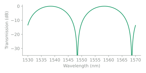
Learn more: Quick Start II: Passive, Key Concepts, Circuit Model
Local GUI
The local GUI runs on your computer and opens from Python. It shows the layout and the schematic side by side, with the PDK library, routing tools and design-rule checks. Edits in the GUI and edits in Python apply to the same design.
To open it, run:
from photonforge.live_viewer import LiveViewer

viewer = LiveViewer()
The command prints the address to open in your browser.
To show a component from Python, call viewer(component).
The PDKs you install with pip are listed in the Component Library.
To add one, click PDKs above the library, then Add to library.
A public PDK that is not installed yet is listed under Not installed, with its pip command and an Install button.
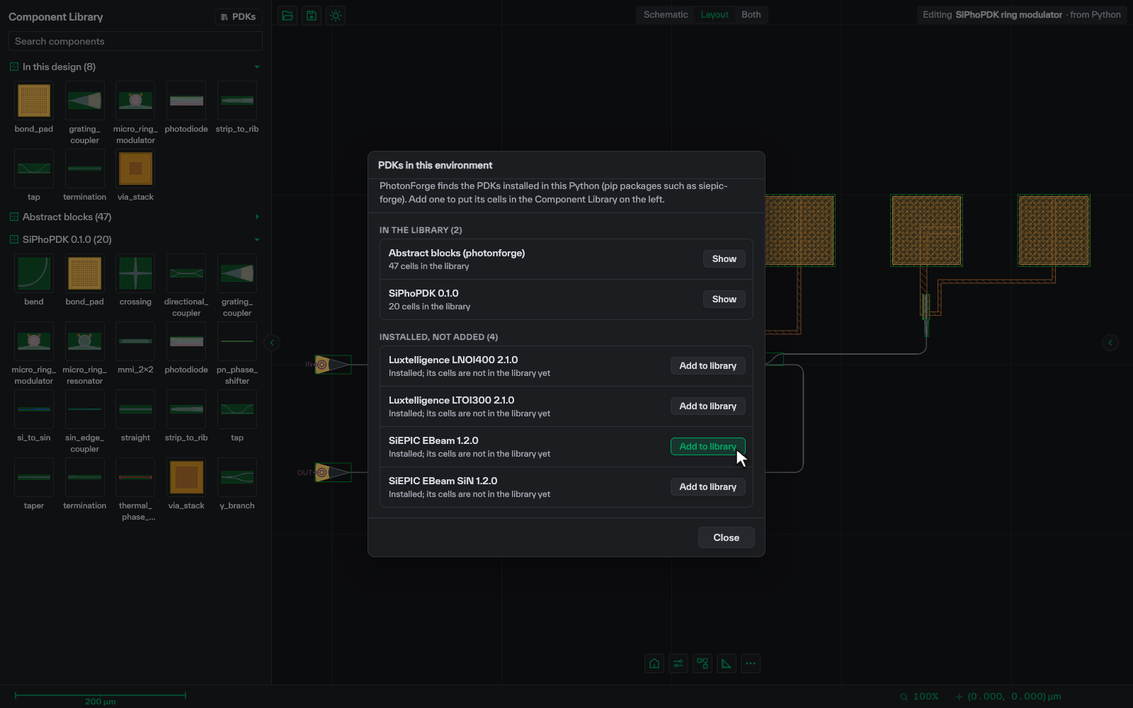
Learn more: Getting Started
AI Agents
Use PhotonForge from the AI coding tool you already use: Claude Code, Codex, Cursor, VS Code or Copilot. The PhotonForge plugin gives the agent skill files (step-by-step instructions for common tasks) and a documentation server. The agent writes PhotonForge code, runs it, and checks the result in the local GUI.
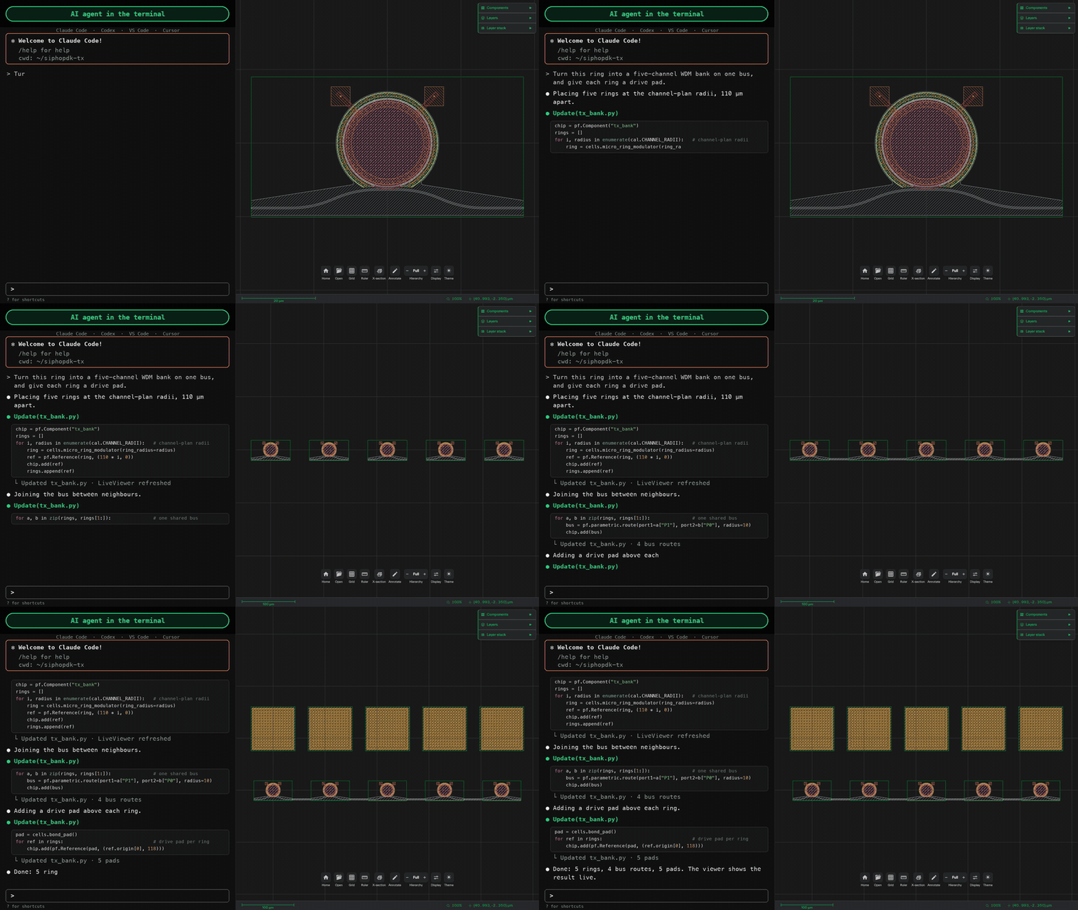
To install the plugin on macOS or Linux, run this command and select PhotonForge:
curl -LsSf https://raw.githubusercontent.com/flexcompute/plugin-marketplace/main/install.sh | bash
Windows instructions and the list of skills are in the plugin repository.
Learn more: AI Agents
EDA Tools
PhotonForge reads and writes GDS and OASIS layouts. The Cadence connector loads PDK cells and parametric cells from Cadence Virtuoso and writes finished layouts back. Virtuoso users can then run Tidy3D multiphysics simulations on their own cells and keep their existing EDA flow for layout and verification. DRC and LVS connectors run the foundry rule decks. Contact us for the EDA connectors.
Learn more: Importing a GDSII/OASIS Layout, Exporting a GDSII/OASIS Layout
PDKs
PDK |
Platform |
Install |
|---|---|---|
SiEPIC EBeam |
Silicon, 220 nm |
|
SiEPIC SiN |
Silicon nitride |
|
Luxtelligence LNOI400 |
Thin-film lithium niobate |
|
Luxtelligence LTOI300 |
Thin-film lithium tantalate |
|
Cornerstone |
Silicon, 220 nm, passive |
Foundry PDKs come with PhotonForge Enterprise. They include PDKs from GlobalFoundries, Tower Semiconductor, AIM Photonics, imec, AMF, Ligentec, Fraunhofer HHI and SMART Photonics. Each foundry PDK also needs your own NDA with the foundry.
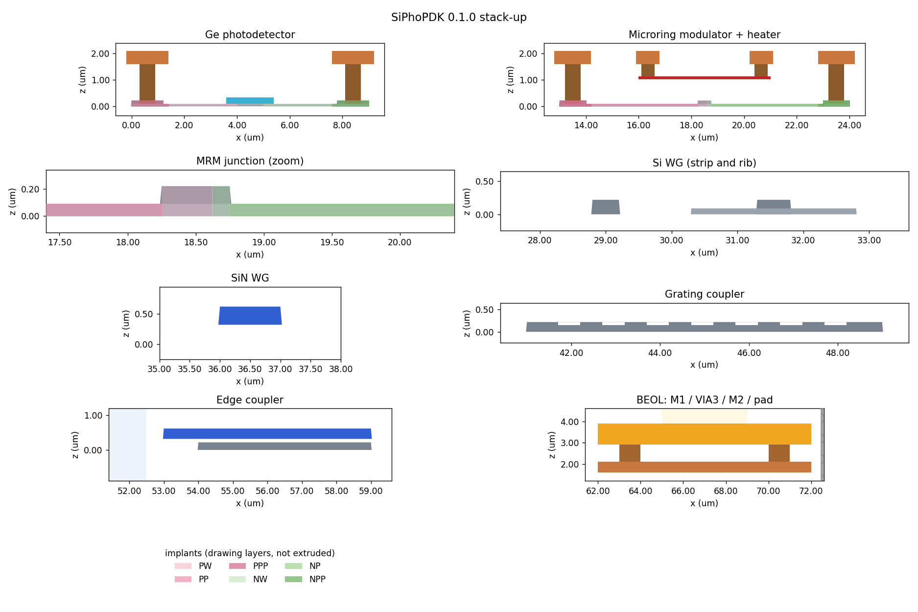
You can also build your own PDK in Python: a technology (layers, layer stack and waveguide cross sections) and a library of parametric cells with models.
Learn more: Custom Technology, Custom Component Library, PDKs
Community and Enterprise
Community: free, unlimited seats
Local GUI with schematic-driven layout
Optical and electrical autorouting
DRC and LVS
Circuit simulation in the time and frequency domain
Integration with Tidy3D (simulations use FlexCredits)
AI agents through the PhotonForge plugin
Open PDKs
Enterprise: Photonic Canvas license
Everything in Community, and:
Foundry PDKs, with support and updates
Version control and traceability in Photonic Canvas projects, from design to measured data
EDA connectors for layout and verification
Automated compact model generation (Verilog-A)
On-premises deployment
Contact us about Enterprise.
What Runs Where
On your computer
The PhotonForge Python package and the local GUI
Layout, schematic and routing
Circuit simulation, in the time and frequency domain
DRC, LVS and Verilog-A export
Your files: scripts, notebooks, GDS and OASIS
In the Flexcompute cloud
Tidy3D simulations: FDTD, EME, mode solver, charge, heat and RF, paid in FlexCredits
Photonic Canvas projects for version control and sharing, if you use them
Photonic Canvas also has an on-premises deployment, which keeps projects on your own servers. See Local and Cloud for details.
Questions and Answers
What PhotonForge is and how to start.
Foundries, access, EDA tools, verification and custom PDKs.
Skill files, the documentation server and autonomous design.
Parametric cells, custom models and device simulation.
Netlists, circuit simulation and schematic-driven layout.
Autorouting, length matching, crossings and vias.
Optimization, nonlinear models, Verilog-A and variation.
DRC, LVS and Check Against Source.
What is free and what is in Enterprise.
What runs on your computer and where your data is.
Compact models from measured data.
Version Control, Traceability and Collaboration
Versions, traceability and sharing.