
Signal Integrity Analysis of a 100 Gbps Transmitter
High-speed optical modulators, operating at data rates of >100 Gbps per wavelength channel, requires careful attention to their time-domain response, since bandwidth limitations, dispersion, and non-ideal modulator transfer characteristics can degrade signal integrity and increase bit-error rates.

To evaluate quality of modulated signal in these systems, eye-diagram measurements are usually performed to visualize how the modulated signal evolves over time and reveal timing jitter, distortion, and noise margins.
Using PhotonForge, you can use scattering parameters to build a compact time-domain model of your component to analyze signal integrity, anticipate performance bottlenecks, and optimize design parameters before committing to costly fabrication.
[1]:
import matplotlib.pyplot as plt
import numpy as np
import photonforge as pf
from scipy.signal import bessel, filtfilt
High-speed modulator transfer function
To begin, we create an electro-optic (EO) transfer function. In principle, one can also load experimentally measured EO S21 data as the transfer function.
For a traveling-wave EO modulator in thin-film lithium niobate, the frequency response (EO S21) follows the analytical expression [1]:
Here, \(\omega = 2\pi f\) is the angular microwave frequency,
is the transmission-line input impedance, and
account for forward/backward traveling waves. The propagation constant is \(\gamma_m = \alpha_m - j\, (\omega/c)\, n_m\), where \(n_m\) is the microwave effective index, \(\alpha_m\) the (amplitude) loss rate in Np/m, \(n_{g,\mathrm{opt}}\) the optical group index, \(L\) the modulator length, \(c\) the speed of light in vacuum, \(Z_L\) the load impedance, and \(Z_0\) the characteristic impedance.
Note: The source impedance is assumed equal to the load impedance.
References
Zhu, Di, et al. “Integrated photonics on thin-film lithium niobate.” Advances in Optics and Photonics 13.2 (2021): 242–352, doi: 10.1364/AOP.411024.
[2]:
def Mw(alpha_dB_per_cm_per_sqrtGHz, freq_GHz, n_m, n_g_opt, L_cm, Z_L, Z_0):
    """
    EO S21 of a traveling-wave modulator.

    Parameters
    ----------
    alpha_dB_per_cm_per_sqrtGHz : float
        RF loss coefficient at 1 GHz scaling, in power dB/cm/√GHz.
    freq_GHz : array_like
        Microwave frequency in GHz.
    n_m : float
        Microwave effective index.
    n_g_opt : float
        Optical group index.
    L_cm : float
        Modulator length in cm.
    Z_L, Z_0 : float
        Load and characteristic impedances (ohms).

    Returns
    -------
    m_w : ndarray
        EO S21.
    """
    L = L_cm * 1e-2
    c = 299792458.0
    omega = 2 * np.pi * (freq_GHz * 1e9)

    # dB/cm/√GHz -> Np/m at frequency f (GHz)
    alpha_m = (
        alpha_dB_per_cm_per_sqrtGHz * np.sqrt(freq_GHz) * (np.log(10) / 20.0) * 100.0
    )

    gamma_m = alpha_m - 1j * (omega / c) * n_m

    F_plus = (1 - np.exp(gamma_m * L + 1j * (omega / c) * n_g_opt * L)) / (
        gamma_m * L + 1j * (omega / c) * n_g_opt * L
    )
    F_minus = (1 - np.exp(-gamma_m * L + 1j * (omega / c) * n_g_opt * L)) / (
        -gamma_m * L + 1j * (omega / c) * n_g_opt * L
    )

    Z_in = Z_0 * (Z_L + Z_0 * np.tanh(gamma_m * L)) / (Z_0 + Z_L * np.tanh(gamma_m * L))

    m_w = (
        (2 * Z_in / (Z_in + Z_L))
        * ((Z_L + Z_0) * F_plus + (Z_L - Z_0) * F_minus)
        / ((Z_L + Z_0) * np.exp(gamma_m * L) + (Z_L - Z_0) * np.exp(-gamma_m * L))
    )

    return m_w
We can use our RF and optical solver to estimate these parameters like optical and RF indices, impedances, and also loss. Please refer to our notebook on designing electro-optic Mach-Zehnder Modulator.
[3]:
# Initialize parameters with some nominal values
freq = np.logspace(-1, 2.5, 1001)  # GHz

alpha = 0.75  # dB/cm/sqrt(GHz) Transmission line loss in dB/cm/sqrt(GHz)
n_m = 2.25  # microwave index
n_g_opt = 2.32  # optical group index
L_cm = 1  # modulator length
Z_L = 50  # Assume 50 ohm termination load
Z_0 = 40  # Characteristic impedance of the tranmission line

# Electro-optic S21 calculated analytically
# In reality this will be some measured data but this is good enough for now
EOS21 = Mw(alpha, freq, n_m, n_g_opt, L_cm, Z_L, Z_0)
[4]:
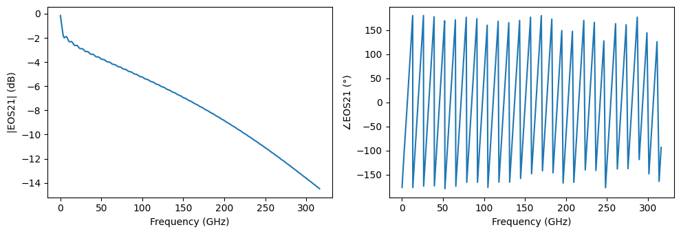
fig, ax = plt.subplots(1, 2, figsize=(10, 3.5), tight_layout=True)

ax[0].plot(freq, 10 * np.log10(np.abs(EOS21) ** 2))
ax[0].set(xlabel="Frequency (GHz)", ylabel="|EOS21| (dB)")

ax[1].plot(freq, np.angle(EOS21, deg=True))
_ = ax[1].set(xlabel="Frequency (GHz)", ylabel="∠EOS21 (°)")
Building a time-domain model
Let’s first create a S-matrix representation in PhotonForge using the pole_residue_fit function.
[5]:
baseband_freqs = freq * 1e9
elements = {("1", "2"): EOS21}
s_matrix = pf.SMatrix(frequencies=baseband_freqs, elements=elements)

# User vector fitting to fit the transfer function before building the time-domain model
pole_res, err = pf.pole_residue_fit(
    s_matrix,
    real=True,
    min_poles=30,
    max_poles=60,
)
s_fit = pole_res(baseband_freqs)

fig, ax = plt.subplots(1, 2, figsize=(10, 3.5), tight_layout=True)

ax[0].plot(freq, np.abs(EOS21))
ax[0].plot(freq, np.abs(s_fit["1", "2"]), "--")
ax[0].set(xlabel="Frequency (GHz)", ylabel="|EOS21|")

ax[1].plot(freq, np.angle(EOS21))
ax[1].plot(freq, np.angle(s_fit["1", "2"]), "--")
_ = ax[1].set(xlabel="Frequency (GHz)", ylabel="∠EOS21 (°)")
/tmp/ipykernel_979312/25767870.py:6: RuntimeWarning: Desired RMS error tolerance not reached: 0.006491881571875424.
  pole_res, err = pf.pole_residue_fit(
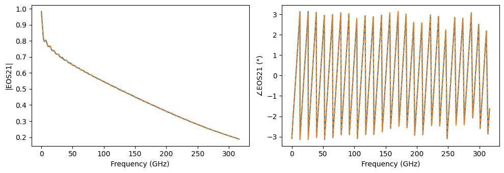
We see a warning about the RMS error tolerance for the fit. That is because the default tolerance is 1.0×10⁻⁴ (a very conservative value) and the fit reached 6×10⁻³. Nonetheless, we can see in the plot that all major features of the transfer function are captured, so we can move forward with this result.
PRBS Signal Generation
Next, we will generate the input electrical signal at 100 Gbps that would be applied to the modulator.
[6]:
# Define parameters
bit_rate = 100e9  # Bit rate (bps)
T = 1 / bit_rate  # Bit period (s)
num_bits = 1000  # Number of bits in PRBS sequence
V = 1  # peak driving voltage

# Desired samples per bit for smoother eye diagram
samples_per_bit = 100
Fs = samples_per_bit * bit_rate  # Sampling frequency
time_step = 1 / Fs  # Time step for simulation

# Time vector
t = np.arange(0, num_bits * T, time_step)

# Generate PRBS sequence
np.random.seed(0)  # For reproducibility
prbs_bits = np.random.randint(0, 2, num_bits)

# Generate NRZ signal
ideal_prbs_signal = np.repeat(prbs_bits, samples_per_bit)
ideal_prbs_signal = V * ideal_prbs_signal[: len(t)]
[7]:
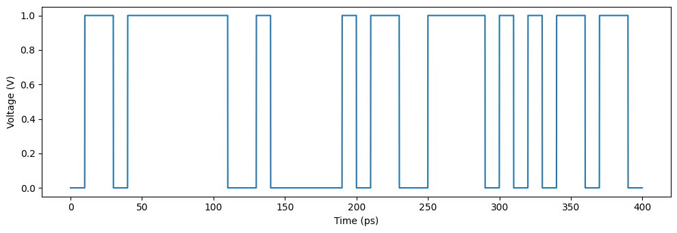
fig, ax = plt.subplots(1, 1, figsize=(10, 3.5), tight_layout=True)
ax.plot(t[:4000] * 1e12, ideal_prbs_signal[:4000])
_ = ax.set(xlabel="Time (ps)", ylabel="Voltage (V)")
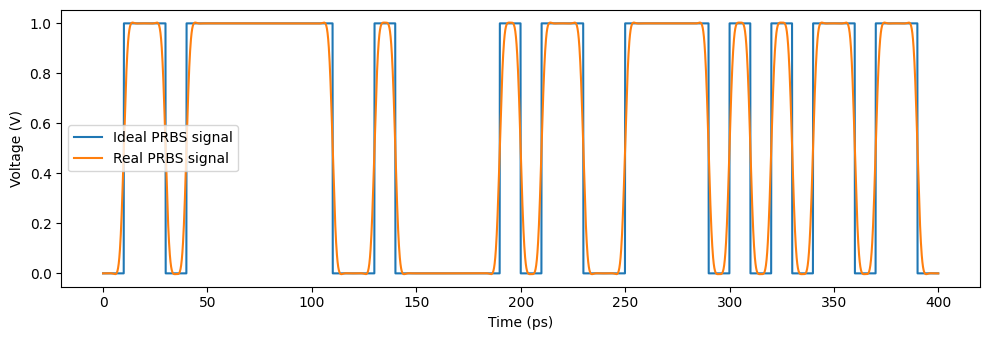
Real electrical systems have some high-frequency cutoff so the signals will not have sharp transitions like we generate above. In simulation, we must also guarantee that the major frequency components of the input signal fall within the valid region in our model, which was fitted up to 300 GHz.
Therefore, we’ll pipe the ideal signal through a 200 GHz low-pass-filter to generate the real electrical input.
[8]:
cutoff_freq = 200e9  # 200 GHz
filter_order = 4

# Normalize the frequency
nyquist_freq = 0.5 * Fs
normalized_cutoff = cutoff_freq / nyquist_freq

# Design Bessel filter
b, a = bessel(N=filter_order, Wn=normalized_cutoff, btype="low", analog=False)

# Apply the filter
real_prbs_signal = filtfilt(b, a, ideal_prbs_signal)
[9]:
fig, ax = plt.subplots(1, 1, figsize=(10, 3.5), tight_layout=True)
ax.plot(t[:4000] * 1e12, ideal_prbs_signal[:4000], label="Ideal PRBS signal")
ax.plot(t[:4000] * 1e12, real_prbs_signal[:4000], label="Real PRBS signal")
ax.set(xlabel="Time (ps)", ylabel="Voltage (V)")
_ = plt.legend()
Build a time domain model
First use the frequency response to build a time-domain model.
[10]:
time_domain_model = pf.TimeDomainModel(pole_res, time_step)
Now, time-step to generate output optical signal as a function of time
[11]:
inputs = pf.TimeSeries(values={"1": real_prbs_signal}, time_step=time_step)
optical_signal = np.abs(time_domain_model.step(inputs=inputs)["2"])
Progress: 100000/100000
[12]:
fig, ax = plt.subplots(1, 1, figsize=(10, 3.5), tight_layout=True)
ax.plot(t[:4000] * 1e12, real_prbs_signal[:4000], label="Input")
ax.plot(t[:4000] * 1e12, optical_signal[:4000], label="Output")
ax.set(xlabel="Time (ps)", ylabel="Amplitude")
_ = plt.legend()
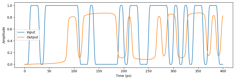
We can use the full sample extent to build an eye diagram.
[13]:
def plot_eye_diagram(optical_output_signal, bit_rate, time_step):
    Fs = 1 / time_step  # sampling frequency
    samples_per_bit = int(0.5 + Fs / bit_rate)

    # Calculate window parameters
    samples_per_window = 2 * samples_per_bit  # 2T window
    start_index = samples_per_window  # Skip initial transients

    # Calculate number of windows
    num_windows = (
        len(optical_output_signal)
        - start_index
        - (samples_per_window - samples_per_bit)
    ) // samples_per_bit
    if num_windows <= 0:
        raise ValueError("Output signal is too short to generate eye diagram.")

    # Extract signal segments for the eye diagram
    parts = []
    for k in range(num_windows):
        idx_start = start_index + k * samples_per_bit
        idx_end = idx_start + samples_per_window
        part = optical_output_signal[idx_start:idx_end]
        parts.append(part)

    parts = np.array(parts).T  # Transpose for time on x-axis

    # Time vector for plotting (centered around 0, in nanoseconds)
    t = (np.arange(samples_per_window) - samples_per_bit) * time_step * 1e12

    # Plotting
    fig, ax = plt.subplots(1, 1, figsize=(7, 4.5), tight_layout=True)
    ax.plot(t, parts, color="yellow", alpha=0.1)
    ax.set(xlabel="Time (ps)", ylabel="Amplitude", facecolor="k", xlim=(t[0], t[-1]))
    ax.grid(ls=":")


plot_eye_diagram(optical_signal, bit_rate, time_step)
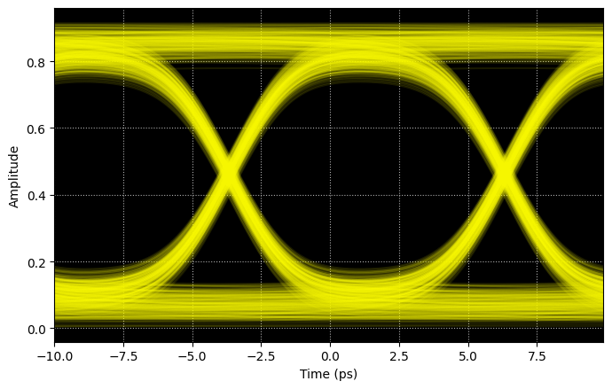
Since this modulator has relatively high bandwidth, it can support high speed modulation and you an see clear eye-opening for this 100 Gbps non-return-to-zero (NRZ) signal.