
Building Circuit Models from Layout Files

In this notebook, we will see how to load GDSII layouts and run both component- and circuit-level simulations. This allows designers to import GDSII files generated from other software tools and evaluate their optical responses.
With a simulation model, we can see how fabrication variations (such as sidewall angles, layer thicknesses, refractive indices, etc.) impact circuit-level performance.
In this demo, we’ll learn how to:
Import hierarchical designs from GDSII files;
Detect ports and assign component models;
Create circuit models; and
Update the fabrication parameters to see impact on the circuit level S matrix.
We begin by first loading libraries for PhotonForge, Tidy3D and the open-source SiEPIC OpenEBL PDK, as well as and others we will require. To install the SiEPIC PDK please follow these steps.
[1]:
import matplotlib.pyplot as plt
import numpy as np
import photonforge as pf
import photonforge.live_viewer as live_viewer
import siepic_forge as siepic_pdk
import tidy3d as td
07:26:31 -03 WARNING: The material-library variant 'Palik_Lossless' is
             deprecated and maps to 'Palik_LowLoss' because it contains a tiny
             fitted loss despite its name. Use 'Palik_NoLoss' where available
             for a zero-loss Palik model.
Assign open-source Siepic PDK as our default technolgy and set some configurations.
[2]:
tech = siepic_pdk.ebeam()
pf.config.default_technology = tech

pf.config.default_mesh_refinement = 12  # Decreased accuracy only to run the example

pf.config.svg_labels = False
Let’s begin by loading the GDSII file external_mzi.gds using the load_layout function. This file was created using an open-source PDK software package for fabrication in SiEPIC foundry, meaning the layer-stacks and PDK components adhere to the specifications provided by the foundry.
We can inspect the data, which is loaded as a dictionary of components (GDSII cells) indexed by name.
[3]:
gds_data = pf.load_layout("external_mzi.gds")

for component_name in gds_data.keys():
    print(component_name)
$$$CONTEXT_INFO$$$
straight_L100_N2_CSstrip
delayline_DL0
delayline_DL200
straight_L17p043_N2_CSx_3c6d3aa8
mzi_with_gratings_DL200
bend_euler_CSstrip_A180
bend_euler_CSstrip
straight_L20p358_N2_CSx_23d87c0c
mzi_DL200
straight_L58p878_N2_CSx_33fc2739
ebeam_y_1550
gc_te1550_broadband
We are interested in creating a simulation model for the unbalanced MZI with grating couplers.
If we ignore the "$$$CONTEXT_INFO$$$" cell, which includes all others, we can look for the top-level component with the find_top_level helper function:
[4]:
top_level = pf.find_top_level(v for k, v in gds_data.items() if k[0] != "$")

for component in top_level:
    print(component.name)
mzi_with_gratings_DL200
[5]:
mzi_circuit = top_level[0]
mzi_circuit
[5]:

[6]:
type(mzi_circuit)
[6]:
photonforge.Component
If we want to inspect the device geometry carefully, we can use the browser-based layout viewer.
[7]:
from photonforge.live_viewer import LiveViewer

viewer = LiveViewer()
LiveViewer started at http://localhost:39351
[8]:
viewer.display(mzi_circuit)
[8]:

We can also visualize all hierarchical nature of how this GDSII file was created.
Feel free to set interactive = True to visualize the components in this heirarchy. We see several independent components such as ebeam_y_1550, gc_te1550_broadband, and bend_euler_CSstrip that make up the circuit.
[9]:
mzi_circuit.tree_view(interactive=False)
[9]:
├─ mzi_DL200
│ ├─ ebeam_y_1550
│ ├─ delayline_DL200
│ │ ├─ bend_euler_CSstrip
│ │ ├─ straight_L100_N2_CSstrip
│ │ └─ bend_euler_CSstrip_A180
│ └─ delayline_DL0
│ ├─ bend_euler_CSstrip
│ └─ bend_euler_CSstrip_A180
├─ gc_te1550_broadband
├─ bend_euler_CSstrip
├─ straight_L17p043_N2_CSx_3c6d3aa8
├─ straight_L58p878_N2_CSx_33fc2739
└─ straight_L20p358_N2_CSx_23d87c0c
GDSII files contains only layout information. In order to build a circuit model, we will identify all components with no dependencies (leaves in the dependency tree) and specify their ports and models to calculate their individual S parameters. PhotonForge will then use the physical connections between them to build the circuit model.
Let us start by looking at all the dependencies of the mzi_circuit component. To identify independent components we need to find the ones that have no further references (references in PhotonForge are like instances of components).
[10]:
# Gather all components with no dependencies (no references to other components)
independent_components = [
    c for c in mzi_circuit.dependencies() if len(c.references) == 0
]

# Sort the list by name
independent_components.sort(key=lambda c: c.name)

print("Independent components:")
for i, component in enumerate(independent_components):
    print(f"- [{i}] {component.name}")
Independent components:
- [0] bend_euler_CSstrip
- [1] bend_euler_CSstrip_A180
- [2] ebeam_y_1550
- [3] gc_te1550_broadband
- [4] straight_L100_N2_CSstrip
- [5] straight_L17p043_N2_CSx_3c6d3aa8
- [6] straight_L20p358_N2_CSx_23d87c0c
- [7] straight_L58p878_N2_CSx_33fc2739
Sub-component setup
Now depending on the type of the component we are looking at we might have to add different ports and models. For example, for gc_te1550_broadband, we want to add a data model and an additional Gaussian port. For ebeam_y_1550 we might want to run FDTD simulations. For straight waveguides (or bends with insignificant loss) we might want a semi-analytical waveguide
model.
We will add ports and models to the independent components one by one to show a few details in the process. Later, this process can be completely automated, if needed, based on the expected GDSII contents.
Component 0
[11]:
component = independent_components[0]
viewer.display(component)
[11]:

By inspecting the component in the live viewer, we see that the routes correspond to a 500 nm wide silicon strip waveguide. The PDK provides the default port specification “TE_1550_500” that matches this profile, so we will be using that to find ports. Note that we can easily inspect the ports of any technology.
[12]:
port_spec = tech.ports["TE_1550_500"]
wg_width, _ = port_spec.path_profile_for((1, 0))
wg_width
[12]:
0.5
[13]:
# Automatically detect ports
edge_ports = component.detect_ports([port_spec], on_boundary="xy")
for port in edge_ports:
    print(port)
Port at (0, 0) at 0 deg with spec "Strip TE 1550 nm, w=500 nm"
Port at (10, 10) at 270 deg with spec "Strip TE 1550 nm, w=500 nm"
[14]:
# Add ports
component.add_port(edge_ports)
viewer.display(component)
[14]:

For 2-port routes where we don’t need to include bend losses, the waveguide model can be used to efficiently compute the S parameters from a single mode-solving calculation and the route length. Otherwise, full FDTD models can always be used to completely characterize the geometry.
[15]:
# Use the area of the waveguide polygon in the layer (1,0) and waveguide width to estimate the route length
area = sum(s.area() for s in component.structures[1, 0])
length = area / wg_width
component.add_model(pf.WaveguideModel(length=length), "Waveguide")
print(f"The length of this path is {length:.3f} μm")
The length of this path is 16.637 μm
Component 1
The second component is very similar to the first we processed.
[16]:
component = independent_components[1]
viewer.display(component)
[16]:

[17]:
# We can limit the search for port to a single boundary
edge_ports = component.detect_ports([port_spec], on_boundary="-x")
for port in edge_ports:
    print(port)
Port at (0, 0) at 0 deg with spec "Strip TE 1550 nm, w=500 nm"
Port at (0, 20) at 0 deg with spec "Strip TE 1550 nm, w=500 nm"
[18]:
# Add ports
component.add_port(edge_ports)

# Add model
length = sum(s.area() for s in component.structures[1, 0]) / wg_width
component.add_model(pf.WaveguideModel(length=length), "Waveguide")
print(f"The length of this route is {length:.3f} μm")

viewer.display(component)
The length of this route is 42.817 μm
[18]:

Component 2
[19]:
component = independent_components[2]
viewer.display(component)
[19]:

Because the port on the -x side has a rectangular box around the actual port edge, looking for ports at the exact boundaries will not work, so we add a 200 nm margin to the search:
[20]:
edge_ports = component.detect_ports([port_spec], on_boundary="x", boundary_margin=0.2)
for port in edge_ports:
    print(port)
Port at (-7.4, 0) at 0 deg with spec "Strip TE 1550 nm, w=500 nm"
Port at (7.4, -2.75) at 180 deg with spec "Strip TE 1550 nm, w=500 nm"
Port at (7.4, 2.75) at 180 deg with spec "Strip TE 1550 nm, w=500 nm"
[21]:
# Add ports
component.add_port(edge_ports)

# Add Tidy3D model
component.add_model(pf.Tidy3DModel(port_symmetries=[("P0", "P2", "P1")]), "Tidy3D")

viewer.display(component)
[21]:

Component 3
[22]:
component = independent_components[3]
viewer.display(component)
[22]:

[23]:
edge_ports = component.detect_ports([port_spec], on_boundary="x", boundary_margin=0.2)
component.add_port(edge_ports)
viewer.display(component)
[23]:

The free-space port for the grating coupler is best modeled by a Gaussian port, which can be used to accurately compute the S matrix based on an Tidy3D model. Alternatively, if we have the data available, a data model can be used as in the foundry PIC design example.
If we are not really interested in adding the effects of the grating coupler, a simpler alternative is to add another waveguide port (even if the geometry does not match it) and an analytical 2-port model, as we do below.
[24]:
# Dummy waveguide port
component.add_port(
    pf.Port(component["P0"].center + (30, 0), input_direction=180, spec=port_spec)
)

component.add_model(pf.TwoPortModel(), "Analytical")

viewer.display(component)
[24]:

Components 4 – 7
For the rest of the components which are simply straight waveguides, we add semi-analytical models again. For straight waveguides, PhotonForge automatically calculates the length so we do not need to explicitly specific length argument when specifying WaveguideModel.
[25]:
for component in independent_components[4:]:
    edge_ports = component.detect_ports([port_spec], on_boundary="x")
    component.add_port(edge_ports)
    component.add_model(pf.WaveguideModel(), "WaveguideModel")
[26]:
viewer.display(independent_components[7])
[26]:

Now let’s look at the overall circuit. We can enable reference port drawing to see that all connections are accounted for.
[27]:
pf.config.svg_reference_ports = True

viewer.display(mzi_circuit)
[27]:

We can see that, once ports are defined for individual components, PhotonForge detects the connections, which we can see by inspecting the netlist. The warnings tell us that there are still dangling ports, but that’s expected, because we are not done yet: we did not add ports to the intermediate-level components.
[28]:
mzi_circuit.get_netlist()["connections"]
/tmp/ipykernel_983321/3086015821.py:1: RuntimeWarning: These ports are not connected and will be ignored: 'P1' at (-34.443, -98.878) from reference to 'gc_te1550_broadband', 'P1' at (-7.4, 0) from reference to 'straight_L17p043_N2_CSx_3c6d3aa8', 'P1' at (92.558, -98.878) from reference to 'gc_te1550_broadband', 'P1' at (62.2, 0) from reference to 'straight_L20p358_N2_CSx_23d87c0c'.
  mzi_circuit.get_netlist()["connections"]
[28]:
[((6, 'P0', 1), (8, 'P0', 1)),
 ((6, 'P1', 1), (7, 'P0', 1)),
 ((3, 'P0', 1), (5, 'P0', 1)),
 ((3, 'P1', 1), (4, 'P0', 1)),
 ((2, 'P0', 1), (8, 'P1', 1)),
 ((1, 'P0', 1), (5, 'P1', 1))]
Circuit ports and models
In our case we want the ports for the grating coupler references to be the final ports. Because the component has a hierarchical structure, we also need to add reference ports and models to each sub-component like mzi_DL200, delayline_DL200 and so on. The add_reference_ports function allows us to recursively add ports and circuit models to these hierarchical
sub-components.
[29]:
mzi_circuit.add_reference_ports(include_dependencies=True, add_model=pf.CircuitModel())

pf.config.svg_reference_ports = False

viewer.display(mzi_circuit)
[29]:

S-matrix computation
Now that ports and models are defined, all we need to do is to call s_matrix on the top-level component.
[30]:
wavelengths = np.linspace(1.545, 1.55, 101)

s_matrix_initial = mzi_circuit.s_matrix(pf.C_0 / wavelengths)
Uploading task 'P0@0…'
Uploading task 'P1@0…'
Uploading task 'Mode-StripTE1550nmw500nm…'
Uploading task 'Mode-StripTE1550nmw500nm…'
Uploading task 'Mode-StripTE1550nmw500nm…'
Uploading task 'Mode-StripTE1550nmw500nm…'
Uploading task 'Mode-StripTE1550nmw500nm…'
Uploading task 'Mode-StripTE1550nmw500nm…'
Uploading task 'Mode-StripTE1550nmw500nm…'
Uploading task 'Mode-StripTE1550nmw500nm…'
Uploading task 'P0@0…'
Uploading task 'P1@0…'
Starting task 'P0@0': https://tidy3d.simulation.cloud/workbench?taskId=fdve-d3638ba7-7781-4b8f-a902-3d4ee7403c79
Starting task 'Mode-StripTE1550nmw500nm': https://tidy3d.simulation.cloud/workbench?taskId=mo-6478b89a-0d2d-4dd7-b904-615c5af988d1
Starting task 'Mode-StripTE1550nmw500nm': https://tidy3d.simulation.cloud/workbench?taskId=mo-4027d34b-1d2e-459e-b441-34b147cb10b9
Starting task 'Mode-StripTE1550nmw500nm': https://tidy3d.simulation.cloud/workbench?taskId=mo-7e6bc3d6-7b08-4cfe-bfb6-44e26e5aebbe
Downloading data from 'P0@0'…
Downloading data from 'Mode-StripTE1550nmw500nm'…
Downloading data from 'Mode-StripTE1550nmw500nm'…
Starting task 'P1@0': https://tidy3d.simulation.cloud/workbench?taskId=fdve-4b96ddb6-92c4-480e-99c8-1e31ab9cf93d
Downloading data from 'Mode-StripTE1550nmw500nm'…
Starting task 'Mode-StripTE1550nmw500nm': https://tidy3d.simulation.cloud/workbench?taskId=mo-4842ce79-f28a-4874-ae1c-afd126244f9e
Starting task 'Mode-StripTE1550nmw500nm': https://tidy3d.simulation.cloud/workbench?taskId=mo-c85439aa-47b7-4b76-be28-a871564fa08a
Starting task 'Mode-StripTE1550nmw500nm': https://tidy3d.simulation.cloud/workbench?taskId=mo-3a971c88-8309-4dc5-b264-31efd74b393d
Downloading data from 'P1@0'…
Starting task 'P0@0': https://tidy3d.simulation.cloud/workbench?taskId=fdve-e11cbd0c-cc5c-41fe-8a99-02cfd13c1bc8
Starting task 'P1@0': https://tidy3d.simulation.cloud/workbench?taskId=fdve-0c4b5962-9f70-4480-855b-eb4e749663dc
Downloading data from 'Mode-StripTE1550nmw500nm'…
Downloading data from 'Mode-StripTE1550nmw500nm'…
Downloading data from 'Mode-StripTE1550nmw500nm'…
Starting task 'Mode-StripTE1550nmw500nm': https://tidy3d.simulation.cloud/workbench?taskId=mo-4aeb32ef-2e50-4953-b037-2a2155447f0d
Starting task 'Mode-StripTE1550nmw500nm': https://tidy3d.simulation.cloud/workbench?taskId=mo-abdfa774-2f5b-44ef-927b-5907870fb885
Downloading data from 'P0@0'…
Downloading data from 'P1@0'…
Downloading data from 'Mode-StripTE1550nmw500nm'…
Downloading data from 'Mode-StripTE1550nmw500nm'…
Progress: 100%
[31]:
_ = pf.plot_s_matrix(s_matrix_initial, input_ports=["P0"])
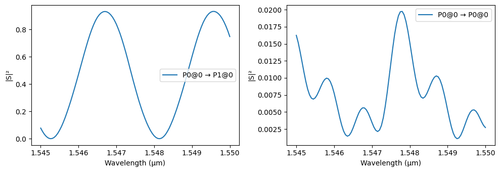
Let us calculate the FSR for the MZI based on the group index of the routing waveguide and compare to the value we can extract from the S parameters.
[32]:
lda = 1.55

mode_solver = pf.port_modes(
    port_spec, frequencies=[pf.C_0 / lda], mesh_refinement=40, group_index=True
)
mode_solver.data.to_dataframe()
Starting…
07:27:02 -03 Loading simulation from local cache. View cached task using web UI
             at
             'https://tidy3d.simulation.cloud/workbench?taskId=mo-26ab46e3-18f4-
             4bbd-86e6-6ef7c213d21c'.
Progress: 100%
[32]:
| wavelength | n eff | k eff | loss (dB/cm) | TE (Ey) fraction | wg TE fraction | wg TM fraction | mode area | group index | dispersion (ps/(nm km)) | ||
|---|---|---|---|---|---|---|---|---|---|---|---|
| f | mode_index | ||||||||||
| 1.934145e+14 | 0 | 1.55 | 2.442662 | 0.0 | 0.0 | 0.983483 | 0.763836 | 0.817709 | 0.190931 | 4.186253 | 508.873435 |
[33]:
dl = 200
ng = mode_solver.data.n_group.isel(mode_index=0, f=0).item()
fsr = lda**2 / (ng * dl)

print(
    f"Estimated FSR from group index calculation using mode solver is {fsr * 1e3:.2f} nm"
)
Estimated FSR from group index calculation using mode solver is 2.87 nm
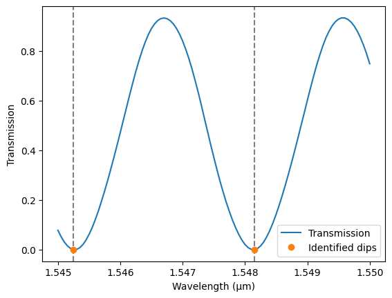
We can get the FSR from the S parameters using scipy to find the transmission dips:
[34]:
from scipy.signal import find_peaks

# We can calculate FSR from the data
transmission = np.abs(s_matrix_initial["P0@0", "P1@0"]) ** 2

# Find dips by inverting the signal: adjust prominence and distance as needed
dips, properties = find_peaks(-transmission, prominence=0.01, distance=5)

# Plot original data
_, ax = plt.subplots(1, 1)
ax.plot(wavelengths, transmission, label="Transmission")

# Plot identified dips
for dip in dips:
    ax.axvline(wavelengths[dip], ls="--", color="tab:gray")

ax.plot(wavelengths[dips], transmission[dips], "o", label="Identified dips")

ax.set(xlabel="Wavelength (µm)", ylabel="Transmission")
ax.legend()

fsr_s = wavelengths[dips[1]] - wavelengths[dips[0]]
print(f"FSR from S-matrix is: {fsr_s * 1e3:.2f} nm")
FSR from S-matrix is: 2.85 nm
Technology variations
During fabrication a number of parameters like the thickness of silicon, sidewall angle, and even material parameters may vary across the wafer. In order to study the impact of these parameters on the performance of the circuit, we can simply update the technology and re-run S-matrix computation.
[35]:
# Since the technology itself is parametric we can inspect what parameters we can update
for k, v in tech.parametric_kwargs.items():
    s = str(v)
    if len(s) > 16:
        s = f"{v.__class__.__name__}(…)"
    print(f"- {k} = {s}")
- si_thickness = 0.22
- si_slab_thickness = 0.09
- si_mask_dilation = 0.0
- si_slab_mask_dilation = 0.0
- sidewall_angle = 0.0
- heater_thickness = 0.2
- router_thickness = 0.6
- bottom_oxide_thickness = 2.0
- top_oxide_thickness = 2.2
- passivation_oxide_thickness = 0.3
- sio2 = dict(…)
- si = dict(…)
- router_metal = dict(…)
- heater_metal = dict(…)
- opening = Medium(…)
Now, let’s update the silicon thickness and see the impact of that on our s-matrix.
[36]:
_ = tech.update(si_thickness=0.215)

s_matrix_thin = mzi_circuit.s_matrix(pf.C_0 / wavelengths)

# It's a good idea to reset the value to the original, in case we forget later
_ = tech.update(si_thickness=0.2)
Uploading task 'P0@0…'
Uploading task 'P1@0…'
Uploading task 'Mode-StripTE1550nmw500nm…'
Uploading task 'Mode-StripTE1550nmw500nm…'
Uploading task 'Mode-StripTE1550nmw500nm…'
Uploading task 'Mode-StripTE1550nmw500nm…'
Uploading task 'Mode-StripTE1550nmw500nm…'
Uploading task 'Mode-StripTE1550nmw500nm…'
Uploading task 'Mode-StripTE1550nmw500nm…'
Uploading task 'Mode-StripTE1550nmw500nm…'
Uploading task 'P0@0…'
Uploading task 'P1@0…'
Starting task 'Mode-StripTE1550nmw500nm': https://tidy3d.simulation.cloud/workbench?taskId=mo-4846bf29-8fba-407c-bc15-69c31bd4ab8b
Starting task 'P1@0': https://tidy3d.simulation.cloud/workbench?taskId=fdve-f797f228-f5e3-4df1-a77e-ab5e8bec2c35
Downloading data from 'Mode-StripTE1550nmw500nm'…
Downloading data from 'P1@0'…
Starting task 'Mode-StripTE1550nmw500nm': https://tidy3d.simulation.cloud/workbench?taskId=mo-0d4af63e-2525-4cc5-8715-0276542e4424
Starting task 'Mode-StripTE1550nmw500nm': https://tidy3d.simulation.cloud/workbench?taskId=mo-c5d16da1-32cd-4139-99c0-a19df106d7e7
Starting task 'P0@0': https://tidy3d.simulation.cloud/workbench?taskId=fdve-461b80c2-bee8-4261-9434-8d0529c406d6
Starting task 'Mode-StripTE1550nmw500nm': https://tidy3d.simulation.cloud/workbench?taskId=mo-651849ae-9181-42eb-bcfa-9a0fa6b3d336
Downloading data from 'Mode-StripTE1550nmw500nm'…
Downloading data from 'Mode-StripTE1550nmw500nm'…
Downloading data from 'P0@0'…
Starting task 'Mode-StripTE1550nmw500nm': https://tidy3d.simulation.cloud/workbench?taskId=mo-3b20d1df-e68c-49b5-b576-fbd1e7ccc66f
Starting task 'Mode-StripTE1550nmw500nm': https://tidy3d.simulation.cloud/workbench?taskId=mo-c1fe319e-0dc8-4cdf-8b96-323697f2c819
Starting task 'Mode-StripTE1550nmw500nm': https://tidy3d.simulation.cloud/workbench?taskId=mo-3c67b6d6-b4a3-4a6a-b03e-aa55648479fa
Downloading data from 'Mode-StripTE1550nmw500nm'…
Downloading data from 'Mode-StripTE1550nmw500nm'…
Downloading data from 'Mode-StripTE1550nmw500nm'…
Downloading data from 'Mode-StripTE1550nmw500nm'…
Starting task 'Mode-StripTE1550nmw500nm': https://tidy3d.simulation.cloud/workbench?taskId=mo-416ee367-5eee-45d5-9cde-8774751c9341
Starting task 'P0@0': https://tidy3d.simulation.cloud/workbench?taskId=fdve-8375c111-b0ff-4de7-baf6-7904c422667c
Downloading data from 'Mode-StripTE1550nmw500nm'…
Downloading data from 'P0@0'…
Starting task 'P1@0': https://tidy3d.simulation.cloud/workbench?taskId=fdve-a64a1fe6-b83a-439b-bfb2-856930616722
Downloading data from 'P1@0'…
Progress: 100%
[37]:
transmission2 = np.abs(s_matrix_thin["P0@0", "P1@0"]) ** 2

_, ax = plt.subplots(1, 1)
ax.plot(wavelengths, transmission, label="Si thickness: 220 nm")
ax.plot(wavelengths, transmission2, label="Si thickness: 200 nm")

ax.set(xlabel="Wavelength (µm)", ylabel="Transmission")
_ = ax.legend()
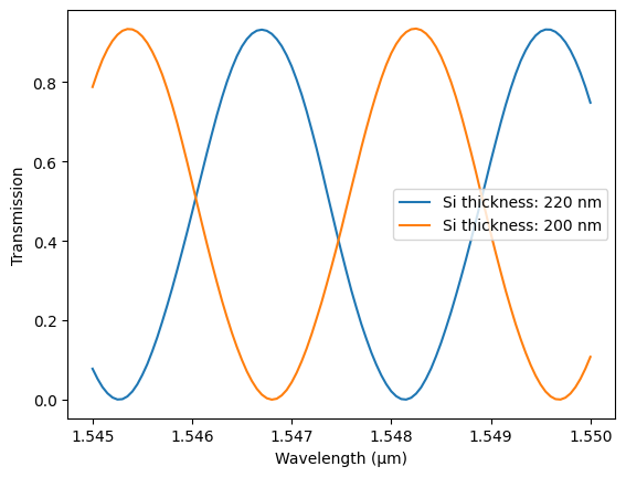
As expected, changing silicon waveguide thinkness across the wafer even by 5 nm will dramatically impact the unbalanced MZM response. One can also perform Monte-Carlo simulations to look at how fabrication variations impact overall circuit performance.
Removing a delay arm
Now, let’s see what happens to the circuit performance if we delete one of the delay arms. We can use the tree view to get the reference numbers within each component:
[38]:
mzi_circuit.tree_view(by_reference=True)
[38]:
├─[0] mzi_DL200
│ ├─[0] ebeam_y_1550
│ ├─[1] delayline_DL200
│ │ ├─[0] bend_euler_CSstrip
│ │ ├─[1] straight_L100_N2_CSstrip
│ │ ├─[2] bend_euler_CSstrip_A180
│ │ ├─[3] straight_L100_N2_CSstrip
│ │ └─[4] bend_euler_CSstrip
│ ├─[2] delayline_DL0
│ │ ├─[0] bend_euler_CSstrip
│ │ ├─[1] bend_euler_CSstrip_A180
│ │ └─[2] bend_euler_CSstrip
│ └─[3] ebeam_y_1550
├─[1] gc_te1550_broadband
├─[2] gc_te1550_broadband
├─[3] bend_euler_CSstrip
├─[4] straight_L17p043_N2_CSx_3c6d3aa8
├─[5] straight_L58p878_N2_CSx_33fc2739
├─[6] bend_euler_CSstrip
├─[7] straight_L20p358_N2_CSx_23d87c0c
└─[8] straight_L58p878_N2_CSx_33fc2739
[39]:
# from the tree view, remove delayline_DL0 from mzi_DL200
mzi_circuit.references[0].component.remove(
    mzi_circuit.references[0].component.references[2]
)
[39]:

[40]:
viewer.display(mzi_circuit)
[40]:

[41]:
s_matrix_new = mzi_circuit.s_matrix(pf.C_0 / wavelengths)
Starting…
Flexcompute/dev/photonforge-docs/.venv/lib/python3.10/site-packages/photonforge/circuit_base.py:545: RuntimeWarning: These ports are not connected and will be ignored: 'P1' at (7.4, -2.75) from reference to 'ebeam_y_1550', 'P1' at (47.4, -2.75) from reference to 'ebeam_y_1550'.
  netlist = component.get_netlist()
Uploading task 'P0@0…'
Uploading task 'P1@0…'
Uploading task 'Mode-StripTE1550nmw500nm…'
Uploading task 'Mode-StripTE1550nmw500nm…'
Uploading task 'Mode-StripTE1550nmw500nm…'
Uploading task 'Mode-StripTE1550nmw500nm…'
Uploading task 'Mode-StripTE1550nmw500nm…'
Uploading task 'Mode-StripTE1550nmw500nm…'
Uploading task 'Mode-StripTE1550nmw500nm…'
Uploading task 'P0@0…'
Uploading task 'P1@0…'
Starting task 'P0@0': https://tidy3d.simulation.cloud/workbench?taskId=fdve-505a71e3-fd2f-401c-8957-b2e2a1867f9b
Starting task 'Mode-StripTE1550nmw500nm': https://tidy3d.simulation.cloud/workbench?taskId=mo-73d9d569-8a77-49c6-a0db-66235d800b39
Starting task 'P1@0': https://tidy3d.simulation.cloud/workbench?taskId=fdve-61fe078d-c4cb-416f-b583-4725333eedd8
Downloading data from 'P0@0'…
Downloading data from 'Mode-StripTE1550nmw500nm'…
Downloading data from 'P1@0'…
Starting task 'Mode-StripTE1550nmw500nm': https://tidy3d.simulation.cloud/workbench?taskId=mo-4c1d5be7-a4ad-4f2a-bb61-9a2826b1d018
Starting task 'Mode-StripTE1550nmw500nm': https://tidy3d.simulation.cloud/workbench?taskId=mo-83988cfd-4a29-400a-9a4b-89839b22d8b6
Downloading data from 'Mode-StripTE1550nmw500nm'…
Downloading data from 'Mode-StripTE1550nmw500nm'…
Starting task 'Mode-StripTE1550nmw500nm': https://tidy3d.simulation.cloud/workbench?taskId=mo-47b1d463-4cef-4ad8-95f2-7ce5416b8f6d
Starting task 'Mode-StripTE1550nmw500nm': https://tidy3d.simulation.cloud/workbench?taskId=mo-a9d50f2e-ec4e-4df0-bae2-d98bd9a9e44e
Starting task 'Mode-StripTE1550nmw500nm': https://tidy3d.simulation.cloud/workbench?taskId=mo-90aee441-dc3c-4744-a6e2-7c068cbad47b
Starting task 'P0@0': https://tidy3d.simulation.cloud/workbench?taskId=fdve-b6b23deb-f780-4be8-a1d3-05460471ec5d
Starting task 'Mode-StripTE1550nmw500nm': https://tidy3d.simulation.cloud/workbench?taskId=mo-9e6569a9-40cc-4f40-a937-1620ddf95f32
Downloading data from 'Mode-StripTE1550nmw500nm'…
Downloading data from 'Mode-StripTE1550nmw500nm'…
Downloading data from 'Mode-StripTE1550nmw500nm'…
Downloading data from 'P0@0'…
Downloading data from 'Mode-StripTE1550nmw500nm'…
Starting task 'P1@0': https://tidy3d.simulation.cloud/workbench?taskId=fdve-e43adae5-33b9-46af-81df-5241421c46fc
Downloading data from 'P1@0'…
Progress: 100%
[42]:
transmission3 = np.abs(s_matrix_new["P0@0", "P1@0"]) ** 2

_, ax = plt.subplots(1, 1)
ax.plot(wavelengths, 10 * np.log10(transmission), label="Original")
ax.plot(wavelengths, 10 * np.log10(transmission3), label="Disconnected")

ax.set(xlabel="Wavelength (µm)", ylabel="Transmission (dB)")
_ = ax.legend()
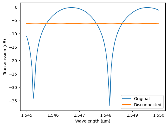
As expected, we see about 6 dB loss from the disconnected splitter.