
Edge Coupler

In this example, we’ll explore the simulation of edge couplers using PhotonForge. Edge couplers are essential components for efficiently coupling light into and out of photonic chips. Typically, optimized edge coupler designs minimize both the insertion loss and the return loss. The geometry of the edge coupler and the medium between the fiber and chip facet significantly impact these performance metrics.
This notebook demonstrates how to use 3D Gaussian Ports in to simulate light emission from a fiber, providing an intuitive approach to simulating scattering matrices for edge couplers. To see how they can also be used with vertical coupling, please refer to the grating coupler example.
We first begin by showing how to set up a Gaussian port to compute the scattering matrix for a simple inverse taper edge coupler. After that, we also look at designing an improved version with an angled edge coupler.
[1]:
import matplotlib.pyplot as plt
import numpy as np
import photonforge as pf
import tidy3d as td
import tidy3d.web as web
We will use the basic technology for Silicon photonics that comes with PhotonForge. One parameter that we will require for positioning our Gaussian port is the thickness of the core layer of our device, so we set it here as well.
[2]:
core_thickness = 0.22

tech = pf.basic_technology(core_thickness=0.22)
pf.config.default_technology = tech
pf.config.default_kwargs["radius"] = 5
Simple Inverse Taper
Let’s build a parametric component to specify our edge coupler, including its ports and model.
We will use the default strip waveguide as base for the inverse taper, so we get a few dimensions from it, knowing that in the basic technology, waveguides are always surrounded by a cladding region.
[3]:
tech
[3]:
Layers
| Name | Layer | Description | Color | Pattern |
|---|---|---|---|---|
| WG_CLAD | (1, 0) | Waveguide clad | #9da6a218 | . |
| WG_CORE | (2, 0) | Waveguide core | #6db5dd18 | / |
| SLAB | (3, 0) | Slab region | #8851ad18 | : |
| TRENCH | (4, 0) | Deep-etched trench for chip…… facets | #535e5918 | + |
| METAL | (5, 0) | Metal layer | #b8a18b18 | \ |
Extrusion Specs
| # | Mask | Limits (μm) | Sidewal (°) | Opt. Medium | Elec. Medium |
|---|---|---|---|---|---|
| 0 | () | -inf, 0 | 0 | cSi_Li1993_293K | Medium(permittivity=12.3) |
| 1 | () | -2, 1.72 | 0 | SiO2_Palik_LowLoss | Medium(permittivity=4.2) |
| 2 | 'WG_CORE' | 0, 0.22 | 0 | cSi_Li1993_293K | Medium(permittivity=12.3) |
| 3 | 'SLAB' | 0, 0.07 | 0 | cSi_Li1993_293K | Medium(permittivity=12.3) |
| 4 | 'METAL' | 1.72, 2.22 | 0 | Cu_JohnsonChristy1972 | PEC |
| 5 | 'TRENCH' | -inf, inf | 0 | Medium() | Medium() |
Ports
| Name | Classification | Description | Width (μm) | Limits (μm) | Radius (μm) | Modes | Target n_eff | Path profiles (μm) | Voltage path | Current path |
|---|---|---|---|---|---|---|---|---|---|---|
| CPW | electrical | CPW transmission line | 18.7398 | -6.46388, 10.4039 | 0 | 1 | 4 | 'gnd0'@……'METAL': 6.8199 (-6.20995), 'gnd1'@'METAL': 6.8199 (+6.20995), 'signal'@'METAL': 3.6 | (2.8, 1.97) (1.8, 1.97) | (2.3, 2.72) (-2.3, 2.72) (-2.3,…… 1.22) (2.3, 1.22) |
| Rib | optical | Rib waveguide | 2.16 | -1, 1.22 | 0 | 1 | 4 | 'WG_CORE': 0.4,…… 'SLAB': 2.4, 'WG_CLAD': 2.4 | ||
| Strip | optical | Strip waveguide | 2.25 | -1, 1.22 | 0 | 1 | 4 | 'WG_CORE': 0.5,…… 'WG_CLAD': 2.5 |
Background medium
- Optical: Medium()
- Electrical: Medium()
[4]:
port_spec = tech.ports["Strip"]
core_width, _ = port_spec.path_profile_for("WG_CORE")
clad_width, _ = port_spec.path_profile_for("WG_CLAD")
[5]:
@pf.parametric_component
def create_edge_coupler(
    *,
    width_tip=0.1,
    length_taper=10,
    waist_radius=2.0,
    fiber_distance=3.0,
    trench_layer="TRENCH"
):
    component = pf.Component()
    component.add(
        "WG_CORE",
        pf.stencil.linear_taper(length_taper, (width_tip, core_width)),
        "WG_CLAD",
        pf.stencil.linear_taper(length_taper, (4 * waist_radius, clad_width)),
    )

    # The Gaussian port must be placed over homogeneous medium, so we add a trench where the
    # port will be placed
    component.add(
        trench_layer,
        pf.Rectangle(
            (-2 * fiber_distance, -3 * waist_radius),
            (0, 3 * waist_radius),
        ),
    )

    port_fiber = pf.GaussianPort(
        center=(-fiber_distance, 0, core_thickness / 2),
        input_vector=(1, 0, 0),
        waist_radius=waist_radius,
        polarization_angle=0,  # for TE mode, in this case
    )
    port_waveguide = pf.Port((length_taper, 0), 180, port_spec)

    component.add_port([port_fiber, port_waveguide])

    model = pf.Tidy3DModel(symmetry=(0, -1, 0))
    component.add_model(model, "Tidy3D")
    return component


create_edge_coupler()
[5]:

Note that we have defined Gaussian port as a source to inject light directly into the waveguide, which is not realistic. We will improve on that later.
For now, let’s create an inverse taper edge coupler with a 150 nm tip and a taper length of 25 μm. We will assume that we are using a lensed fiber of 2.5 μm spot size to couple light into the chip.
[6]:
edge_coupler = create_edge_coupler(
    width_tip=0.15,
    length_taper=25,
    waist_radius=2.5 / 2,
)
edge_coupler
[6]:

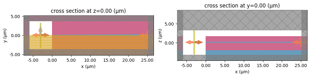
Let’s plot the simulation domain to make sure the Gaussian port is setup properly.
[7]:
wavelengths = np.linspace(1.5, 1.6, 21)

_, ax = plt.subplots(1, 2, figsize=(10, 3), tight_layout=True)

sims = edge_coupler.models["Tidy3D"].get_simulations(edge_coupler, pf.C_0 / wavelengths)
_ = sims["P0@0"].plot(z=0, ax=ax[0])
_ = sims["P0@0"].plot(y=0, ax=ax[1])
07:28:48 -03 WARNING: Structure at 'structures[3]' has bounds that extend
             exactly to simulation edges. This can cause unexpected behavior. If
             intending to extend the structure to infinity along one dimension,
             use td.inf as a size variable instead to make this explicit.
WARNING: Suppressed 2 WARNING messages.
             WARNING: Structure at 'structures[3]' has bounds that extend
             exactly to simulation edges. This can cause unexpected behavior. If
             intending to extend the structure to infinity along one dimension,
             use td.inf as a size variable instead to make this explicit.
WARNING: Suppressed 2 WARNING messages.
Next, we compute and plot the S matrix (limited to a single input, to limit the number of simulations run).
[8]:
s_matrix = edge_coupler.s_matrix(pf.C_0 / wavelengths, model_kwargs={"inputs": ["P0"]})
_ = pf.plot_s_matrix(s_matrix, y="dB", threshold=0.2, input_ports=["P0"])
Starting…
             WARNING: Structure at 'structures[3]' has bounds that extend
             exactly to simulation edges. This can cause unexpected behavior. If
             intending to extend the structure to infinity along one dimension,
             use td.inf as a size variable instead to make this explicit.
WARNING: Suppressed 2 WARNING messages.
07:28:49 -03 WARNING: Structure at 'structures[3]' has bounds that extend
             exactly to simulation edges. This can cause unexpected behavior. If
             intending to extend the structure to infinity along one dimension,
             use td.inf as a size variable instead to make this explicit.
WARNING: Suppressed 2 WARNING messages.
             WARNING: Structure at 'structures[3]' has bounds that extend
             exactly to simulation edges. This can cause unexpected behavior. If
             intending to extend the structure to infinity along one dimension,
             use td.inf as a size variable instead to make this explicit.
WARNING: Suppressed 2 WARNING messages.
Uploading task 'P0@0…'
             WARNING: Structure at 'structures[3]' has bounds that extend
             exactly to simulation edges. This can cause unexpected behavior. If
             intending to extend the structure to infinity along one dimension,
             use td.inf as a size variable instead to make this explicit.
WARNING: Suppressed 2 WARNING messages.
             WARNING: Structure at 'structures[3]' has bounds that extend
             exactly to simulation edges. This can cause unexpected behavior. If
             intending to extend the structure to infinity along one dimension,
             use td.inf as a size variable instead to make this explicit.
WARNING: Suppressed 2 WARNING messages.
Uploading task 'P1…'Progress: 0% \
Starting task 'P0@0': https://tidy3d.simulation.cloud/workbench?taskId=fdve-6520a089-5c40-46a3-85d6-7d5e2c11f14f
Downloading data from 'P0@0'…
Starting task 'P1': https://tidy3d.simulation.cloud/workbench?taskId=mo-5dd0dd87-1cba-4f9e-96bc-c86ebb363234
Downloading data from 'P1'…
Progress: 98% |
07:29:13 -03 WARNING: Structure at 'structures[3]' has bounds that extend
             exactly to simulation edges. This can cause unexpected behavior. If
             intending to extend the structure to infinity along one dimension,
             use td.inf as a size variable instead to make this explicit.
WARNING: Suppressed 2 WARNING messages.
             WARNING: Warning messages were found in the solver log. For more
             information, check 'SimulationData.log' or use
             'web.download_log(task_id)'.
Progress: 100%
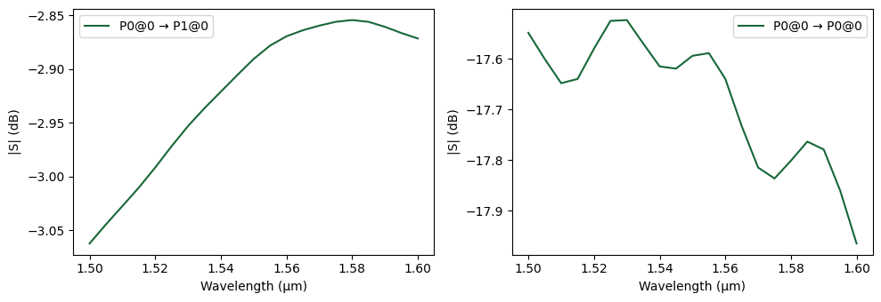
We see an insertion loss above 2.7 dB in the whole wavelength range, which includes both modal mismatch and reflections from the chip facet.
Index-Matched Gap
Index matching fluid or packaging epoxy can be used to not only improve the coupling efficiency but also to provide structural support post packaging. In order to see how adding an index matching layer affects the coupling losses while keeping the fiber at a fixed distance away from the chip we will define a new layer and an extrusion specification.
We could, in this case, set the basic technology parameter trench_medium to the index matching fluid to the same effect, but this is a good example of technology customization that might be useful in cases where the technology function does not provide enough flexibility.
First, we define and add the new layer:
[9]:
matching_layer = pf.LayerSpec(
    (5, 0), "Index matching region", color=(30, 30, 155, 100), pattern="x"
)
tech.add_layer("INDEX_MATCHING", matching_layer)
tech.layers
[9]:
| Name | Layer | Description | Color | Pattern |
|---|---|---|---|---|
| WG_CLAD | (1, 0) | Waveguide clad | #9da6a218 | . |
| WG_CORE | (2, 0) | Waveguide core | #6db5dd18 | / |
| SLAB | (3, 0) | Slab region | #8851ad18 | : |
| TRENCH | (4, 0) | Deep-etched trench for chip…… facets | #535e5918 | + |
| INDEX_MATCHING | (5, 0) | Index matching region | #1e1e9b64 | x |
| METAL | (5, 0) | Metal layer | #b8a18b18 | \ |
Then, we create a new extrusion specification to extrude the structures in our new layer with the appropriate dimensions and medium. Typically, the index of the index matching layer is close to but lower than the index of the SiO₂ cladding, so we will use refractive index of 1.4 for this simulation.
Note that this extrusion will be inserted after the core and slab extrusion rules, because we might want to override the structures from those steps with the index matching region.
[10]:
medium_index_matching = td.Medium(permittivity=1.4**2, name="INDEX_MATCHING")
matching_extrusion = pf.ExtrusionSpec(
    pf.MaskSpec("INDEX_MATCHING"), medium_index_matching, (-pf.Z_INF, pf.Z_INF)
)
tech.insert_extrusion_spec(len(tech.extrusion_specs), matching_extrusion)
tech.extrusion_specs
[10]:
| # | Mask | Limits (μm) | Sidewal (°) | Opt. Medium | Elec. Medium |
|---|---|---|---|---|---|
| 0 | () | -inf, 0 | 0 | cSi_Li1993_293K | Medium(permittivity=12.3) |
| 1 | () | -2, 1.72 | 0 | SiO2_Palik_LowLoss | Medium(permittivity=4.2) |
| 2 | 'WG_CORE' | 0, 0.22 | 0 | cSi_Li1993_293K | Medium(permittivity=12.3) |
| 3 | 'SLAB' | 0, 0.07 | 0 | cSi_Li1993_293K | Medium(permittivity=12.3) |
| 4 | 'INDEX_MATCHING' | 1.72, 2.22 | 0 | Cu_JohnsonChristy1972 | PEC |
| 5 | 'TRENCH' | -inf, inf | 0 | Medium() | Medium() |
| 6 | 'INDEX_MATCHING' | -inf, inf | 0 | INDEX_MATCHING | INDEX_MATCHING |
[11]:
edge_coupler = create_edge_coupler(
    width_tip=0.15,
    length_taper=25,
    waist_radius=2.5 / 2,
    fiber_distance=3,
    trench_layer="INDEX_MATCHING",
)
edge_coupler
[11]:

[12]:
_, ax = plt.subplots(1, 2, figsize=(10, 3), tight_layout=True)

sims = edge_coupler.models["Tidy3D"].get_simulations(edge_coupler, pf.C_0 / wavelengths)
_ = sims["P0@0"].plot(z=0, ax=ax[0])
_ = sims["P0@0"].plot(y=0, ax=ax[1])
07:29:17 -03 WARNING: Structure at 'structures[3]' has bounds that extend
             exactly to simulation edges. This can cause unexpected behavior. If
             intending to extend the structure to infinity along one dimension,
             use td.inf as a size variable instead to make this explicit.
WARNING: Suppressed 5 WARNING messages.
             WARNING: Structure at 'structures[3]' has bounds that extend
             exactly to simulation edges. This can cause unexpected behavior. If
             intending to extend the structure to infinity along one dimension,
             use td.inf as a size variable instead to make this explicit.
WARNING: Suppressed 5 WARNING messages.
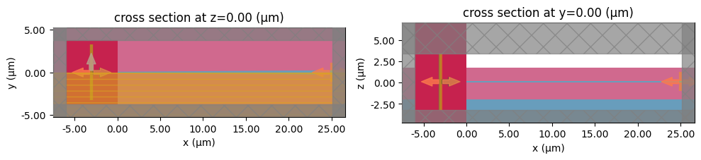
Next, we calculate the S parameters and plot it.
[13]:
s_matrix_matched = edge_coupler.s_matrix(
    pf.C_0 / wavelengths, model_kwargs={"inputs": ["P0"]}
)
_ = pf.plot_s_matrix(s_matrix_matched, y="dB", input_ports=["P0"])
Starting…
07:29:18 -03 WARNING: Structure at 'structures[3]' has bounds that extend
             exactly to simulation edges. This can cause unexpected behavior. If
             intending to extend the structure to infinity along one dimension,
             use td.inf as a size variable instead to make this explicit.
WARNING: Suppressed 5 WARNING messages.
             WARNING: Structure at 'structures[3]' has bounds that extend
             exactly to simulation edges. This can cause unexpected behavior. If
             intending to extend the structure to infinity along one dimension,
             use td.inf as a size variable instead to make this explicit.
WARNING: Suppressed 5 WARNING messages.
Uploading task 'P0@0…'
             WARNING: Structure at 'structures[3]' has bounds that extend
             exactly to simulation edges. This can cause unexpected behavior. If
             intending to extend the structure to infinity along one dimension,
             use td.inf as a size variable instead to make this explicit.
WARNING: Suppressed 5 WARNING messages.
             WARNING: Structure at 'structures[3]' has bounds that extend
             exactly to simulation edges. This can cause unexpected behavior. If
             intending to extend the structure to infinity along one dimension,
             use td.inf as a size variable instead to make this explicit.
WARNING: Suppressed 4 WARNING messages.
             WARNING: Structure at 'structures[3]' has bounds that extend
             exactly to simulation edges. This can cause unexpected behavior. If
             intending to extend the structure to infinity along one dimension,
             use td.inf as a size variable instead to make this explicit.
WARNING: Suppressed 3 WARNING messages.
             WARNING: Structure at 'structures[3]' has bounds that extend
             exactly to simulation edges. This can cause unexpected behavior. If
             intending to extend the structure to infinity along one dimension,
             use td.inf as a size variable instead to make this explicit.
Uploading task 'P1…'
Progress: 0% \
             WARNING: Structure at 'structures[3]' has bounds that extend
             exactly to simulation edges. This can cause unexpected behavior. If
             intending to extend the structure to infinity along one dimension,
             use td.inf as a size variable instead to make this explicit.
             WARNING: Structure at 'structures[4]' has bounds that extend
             exactly to simulation edges. This can cause unexpected behavior. If
             intending to extend the structure to infinity along one dimension,
             use td.inf as a size variable instead to make this explicit.
Starting task 'P0@0': https://tidy3d.simulation.cloud/workbench?taskId=fdve-fd73b7f2-aa4b-4d31-801f-f83885de3868
Starting task 'P1': https://tidy3d.simulation.cloud/workbench?taskId=mo-09c45bbf-9818-4a25-9fac-aaa97488858c
Downloading data from 'P0@0'…
Downloading data from 'P1'…
Progress: 98% \
07:29:42 -03 WARNING: Structure at 'structures[3]' has bounds that extend
             exactly to simulation edges. This can cause unexpected behavior. If
             intending to extend the structure to infinity along one dimension,
             use td.inf as a size variable instead to make this explicit.
WARNING: Suppressed 5 WARNING messages.
             WARNING: Warning messages were found in the solver log. For more
             information, check 'SimulationData.log' or use
             'web.download_log(task_id)'.
Progress: 100%
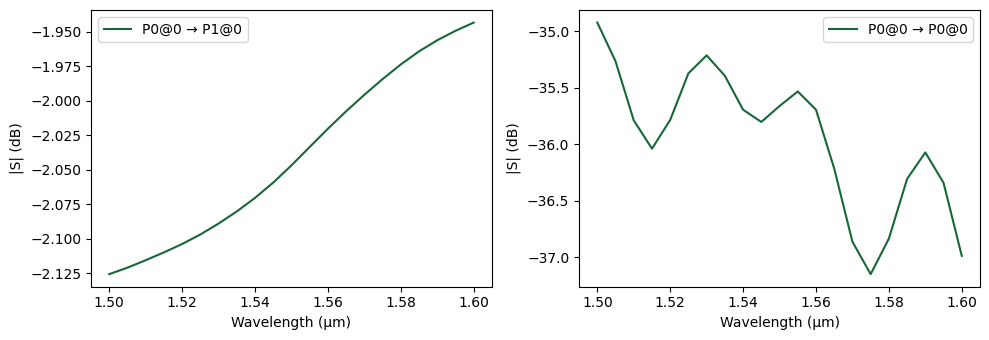
By introducing the index matching region, we are able to increase the coupling efficiency by almost 1 dB, as well as reduce the reflections to less than -35 dB. From this point, we could further characterize how the position and angular alignment of the fiber affects the insertion and return losses.
Another interesting possibility is to use an angled taper to minimize return losses, which is critical in some applications and offers us the opportunity to demonstrate angled waveguide and Gaussian ports.
Angled Inverse Taper
We will begin by creating a parametric function that allows us to create an angled edge coupler. At the output of the edge coupler, we will create an angled waveguide. A small bend is also added to guarantee a grid_aligned port.
[14]:
@pf.parametric_component
def create_angled_edge_coupler(
    *,
    width_tip=0.1,
    length_taper=10,
    angle_taper=7,
    waist_radius=2.0,
    fiber_distance=3.0,
    angle_fiber=10.2,
    trench_size_factor=3.0,
    trench_layer="TRENCH"
):

    v_taper = np.array(
        (np.cos(angle_taper / 180 * np.pi), np.sin(angle_taper / 180 * np.pi))
    )
    v_fiber = np.array(
        (np.cos(angle_fiber / 180 * np.pi), np.sin(angle_fiber / 180 * np.pi))
    )

    # Build the silicon inverse taper
    endpoint = pf.snap_to_grid(length_taper * v_taper)
    taper_core = (
        pf.Path(-waist_radius * v_taper, width_tip)
        .segment((0, 0))
        .segment(endpoint, core_width)
    )
    taper_clad = (
        pf.Path(-waist_radius * v_taper, 4 * waist_radius)
        .segment((0, 0))
        .segment(length_taper * v_taper, clad_width)
    )

    # Taper endpoint after a small bend to guarantee that the waveguide port
    # grid-aligned
    if angle_taper > 0:
        radius = pf.config.default_kwargs["radius"]
        endpoint = pf.snap_to_grid(
            endpoint + radius * np.array((abs(v_taper[1]), 1 - v_taper[0]))
        )
        base = 90 if angle_taper > 0 else -90
        taper_core.arc(90 + angle_taper, 90, radius, endpoint=endpoint)
        taper_clad.arc(90 + angle_taper, 90, radius, endpoint=endpoint)

    component = pf.Component()
    component.add(
        "WG_CORE",
        taper_core,
        "WG_CLAD",
        taper_clad,
        trench_layer,
        pf.Rectangle(
            (-2 * fiber_distance, -trench_size_factor * waist_radius),
            (0, trench_size_factor * waist_radius),
        ),
    )

    fiber_center = -fiber_distance * v_fiber
    port_fiber = pf.GaussianPort(
        center=(fiber_center[0], fiber_center[1], core_thickness / 2),
        input_vector=(v_fiber[0], v_fiber[1], 0),
        waist_radius=waist_radius,
        polarization_angle=0,  # for TE mode, in this case
    )
    port_waveguide = pf.Port(endpoint, 180, port_spec)

    component.add_port([port_fiber, port_waveguide])

    model = pf.Tidy3DModel()
    component.add_model(model, "Tidy3D")
    return component


create_angled_edge_coupler()
[14]:

[15]:
angle_fiber = 15  # in degrees
# Fresnel diffraction
angle_taper = np.arcsin(np.sin(angle_fiber / 180 * np.pi) / 1.45) / np.pi * 180
print(f"Taper angle: {angle_taper:.1f}°")

edge_coupler = create_angled_edge_coupler(
    width_tip=0.15,
    length_taper=25,
    angle_taper=angle_taper,
    waist_radius=2.5 / 2,
    fiber_distance=3,
    angle_fiber=angle_fiber,
    trench_size_factor=4,
    trench_layer="TRENCH",
)
edge_coupler
Taper angle: 10.3°
[15]:

[16]:
_, ax = plt.subplots(1, 2, figsize=(10, 3), tight_layout=True)
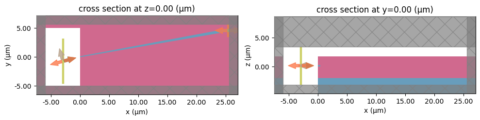
sims = edge_coupler.models["Tidy3D"].get_simulations(edge_coupler, pf.C_0 / wavelengths)
_ = sims["P0@0"].plot(z=0, ax=ax[0])
_ = sims["P0@0"].plot(y=0, ax=ax[1])
07:29:56 -03 WARNING: Structure at 'structures[3]' has bounds that extend
             exactly to simulation edges. This can cause unexpected behavior. If
             intending to extend the structure to infinity along one dimension,
             use td.inf as a size variable instead to make this explicit.
WARNING: Suppressed 1 WARNING message.
             WARNING: Structure at 'structures[3]' has bounds that extend
             exactly to simulation edges. This can cause unexpected behavior. If
             intending to extend the structure to infinity along one dimension,
             use td.inf as a size variable instead to make this explicit.
WARNING: Suppressed 1 WARNING message.
[17]:
s_matrix_tilted = edge_coupler.s_matrix(
    pf.C_0 / wavelengths, model_kwargs={"inputs": ["P0"]}
)
_ = pf.plot_s_matrix(s_matrix_tilted, y="dB", input_ports=["P0"])
Starting…
             WARNING: Structure at 'structures[3]' has bounds that extend
             exactly to simulation edges. This can cause unexpected behavior. If
             intending to extend the structure to infinity along one dimension,
             use td.inf as a size variable instead to make this explicit.
WARNING: Suppressed 1 WARNING message.
Uploading task 'P0@0…'Progress: 0% \
             WARNING: Structure at 'structures[3]' has bounds that extend
             exactly to simulation edges. This can cause unexpected behavior. If
             intending to extend the structure to infinity along one dimension,
             use td.inf as a size variable instead to make this explicit.
WARNING: Suppressed 1 WARNING message.
07:29:57 -03 WARNING: Structure at 'structures[3]' has bounds that extend
             exactly to simulation edges. This can cause unexpected behavior. If
             intending to extend the structure to infinity along one dimension,
             use td.inf as a size variable instead to make this explicit.
WARNING: Suppressed 1 WARNING message.
Starting task 'P0@0': https://tidy3d.simulation.cloud/workbench?taskId=fdve-75181fee-e3ea-4cf8-b82c-c849c2e1ed4a
Downloading data from 'P0@0'…
Progress: 98% \
07:30:25 -03 WARNING: Structure at 'structures[3]' has bounds that extend
             exactly to simulation edges. This can cause unexpected behavior. If
             intending to extend the structure to infinity along one dimension,
             use td.inf as a size variable instead to make this explicit.
WARNING: Suppressed 1 WARNING message.
             WARNING: Warning messages were found in the solver log. For more
             information, check 'SimulationData.log' or use
             'web.download_log(task_id)'.
Progress: 100%
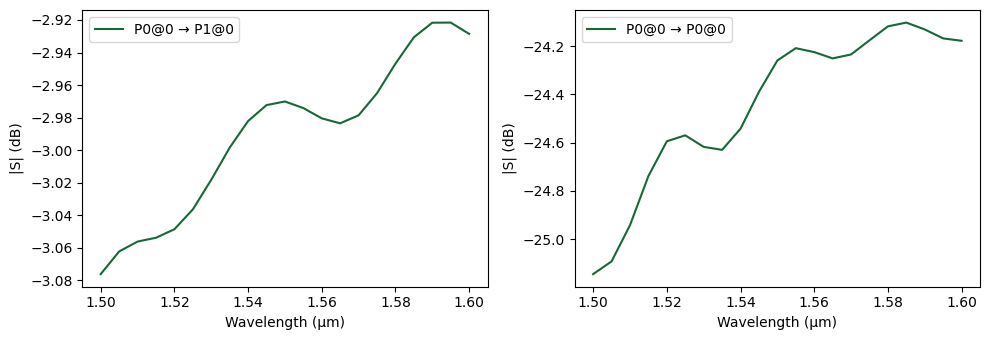
We see that the insertion loss has essentially remained the same when compared to the straight edge coupler with air gap, but the reflection is more than 6 dB lower.