
Ports
Ports are terminals through which electromagnetic waves can enter or exit a system. In PhotonForge, they are 2D surfaces used to connect a component to the external world. The S parameters of a device describes how the electromagnetic fields entering through its ports are transmitted within the component and exit through those same ports.
A technology in PhotonForge comes with a number of predefined port specifications, which describe the waveguide cross-section represented by that port.

Inspecting Ports
We will use the basic technology as an example of technology from a PDK. The ports defined in the technology can be easily inspected:
[1]:
import photonforge as pf

tech = pf.basic_technology()
pf.config.default_technology = tech

tech.ports
[1]:
| Name | Classification | Description | Width (μm) | Limits (μm) | Radius (μm) | Modes | Target n_eff | Path profiles (μm) | Voltage path | Current path |
|---|---|---|---|---|---|---|---|---|---|---|
| CPW | electrical | CPW transmission line | 18.7398 | -6.46388, 10.4039 | 0 | 1 | 4 | 'gnd0'@……'METAL': 6.8199 (-6.20995), 'gnd1'@'METAL': 6.8199 (+6.20995), 'signal'@'METAL': 3.6 | (2.8, 1.97) (1.8, 1.97) | (2.3, 2.72) (-2.3, 2.72) (-2.3,…… 1.22) (2.3, 1.22) |
| Rib | optical | Rib waveguide | 2.16 | -1, 1.22 | 0 | 1 | 4 | 'WG_CORE': 0.4,…… 'SLAB': 2.4, 'WG_CLAD': 2.4 | ||
| Strip | optical | Strip waveguide | 2.25 | -1, 1.22 | 0 | 1 | 4 | 'WG_CORE': 0.5,…… 'WG_CLAD': 2.5 |
As we can see, the basic technology comes with 3 predefined port specifications: “Strip”, “Rib”, and “CPW”, corresponding to waveguides of different cross sections.
The specification width defines the lateral dimension of the waveguide cross-section, including the margins required for evanescent fields in dielectric waveguides. Similarly, the limits contain the lower and upper boundary coordinates for the cross-section in the out-of-plane (z) direction. The actual shapes and materials of the waveguide are
defined by its path profiles, which contain (width, offset, layer) tuples. These tuples are used to generate straight path sections when generating the actual waveguide.

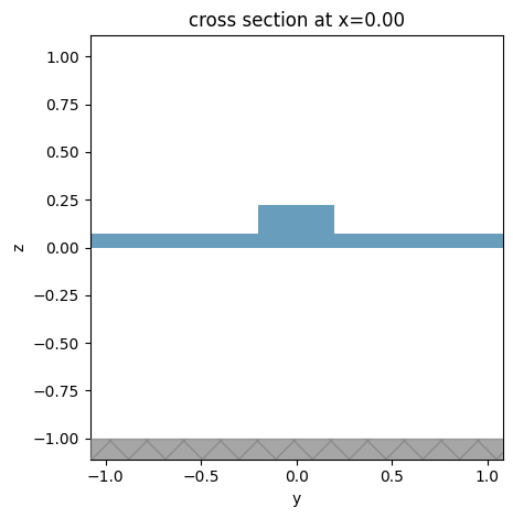
The extrusion profile for the waveguides can be quickly inspected through the tidy3d_plot function:
[2]:
_ = pf.tidy3d_plot(tech.ports["Rib"])
Other attributes of the port specification define its supported modes. In particular, num_modes defines the number of modes used in this specification. For the strip waveguide, num_modes == 1, which means it will support only the fundamental quasi-TE mode. If we wanted to support the first quasi-TM mode too, we could set num_modes = 2. However, if we wanted to support only the quasi-TM mode, we would keep
num_modes == 1 and set added_solver_modes = 1. What added_solver_modes does is include extra modes in the mode solver run, but skip them later, so, in this case, we would solve for 2 modes (TE and TM) and skip the first (TE), keeping only the quasi-TM mode we want.
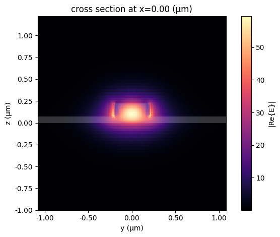
Computing the port specification modes can be easily done though Tidy3D’s mode solver by exporting the specification to tidy3d or directly by using the port_modes function (which uses the cached results).
[3]:
# Increase the mesh refinement for better resolution in field plots
pf.config.default_mesh_refinement = 30

freqs = [pf.C_0 / 1.55]

mode_solver = pf.port_modes("Rib", freqs)
mode_solver.plot_field("E", mode_index=0, f=freqs[0], robust=False)
mode_solver.data.to_dataframe()
Uploading task 'Mode-ModeSolver…'
Starting task 'Mode-ModeSolver': https://tidy3d.simulation.cloud/workbench?taskId=mo-7061f3be-9bc4-4da2-9c58-274989542ed5
Downloading data from 'Mode-ModeSolver'…
Progress: 100%
[3]:
| wavelength | n eff | k eff | loss (dB/cm) | TE (Ey) fraction | wg TE fraction | wg TM fraction | mode area | ||
|---|---|---|---|---|---|---|---|---|---|
| f | mode_index | ||||||||
| 1.934145e+14 | 0 | 1.55 | 2.401763 | 0.0 | 0.0 | 0.976937 | 0.81569 | 0.804108 | 0.208956 |
Finally, additional parameters are available exclusively for electrical port specifications. Because we are focusing at optical frequencies, we will not dive further into those parameters in this guide.
Custom Port Specification
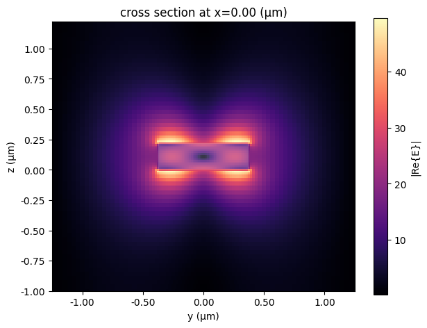
If we need to use a custom waveguide profile, it’s easy to create a new port specification. For example, let’s add a multimode strip profile with an 800 nm core width, and a vertical slot waveguide. Note that we follow the technology defaults of including the cladding region surrounding the waveguide core in the “WG_CLAD” layer (1, 0), expanding beyond the port width.

[4]:
strip_mm = pf.PortSpec(
    "Multimode strip waveguide",
    width=2.5,
    limits=tech.ports["Strip"].limits,
    num_modes=4,
    target_neff=4,
    path_profiles={(2.6, 0, (1, 0)), (0.75, 0, (2, 0))},
)

mode_solver = pf.port_modes(strip_mm, freqs)
mode_solver.plot_field("E", mode_index=3, f=freqs[0], robust=False)
mode_solver.data.to_dataframe()
Uploading task 'Mode-ModeSolver…'
Starting task 'Mode-ModeSolver': https://tidy3d.simulation.cloud/workbench?taskId=mo-d44afdb3-aef4-4903-9930-ff0f59ed6b74
Downloading data from 'Mode-ModeSolver'…
Progress: 100%
[4]:
| wavelength | n eff | k eff | loss (dB/cm) | TE (Ey) fraction | wg TE fraction | wg TM fraction | mode area | ||
|---|---|---|---|---|---|---|---|---|---|
| f | mode_index | ||||||||
| 1.934145e+14 | 0 | 1.55 | 2.663228 | 0.0 | 0.0 | 0.995849 | 0.879197 | 0.809532 | 0.199621 |
| 1 | 1.55 | 2.069579 | 0.0 | 0.0 | 0.955427 | 0.618617 | 0.861616 | 0.346605 | |
| 2 | 1.55 | 1.896065 | 0.0 | 0.0 | 0.035364 | 0.649199 | 0.919316 | 0.399997 | |
| 3 | 1.55 | 1.491854 | 0.0 | 0.0 | 0.153538 | 0.847691 | 0.664743 | 0.766359 |
[5]:
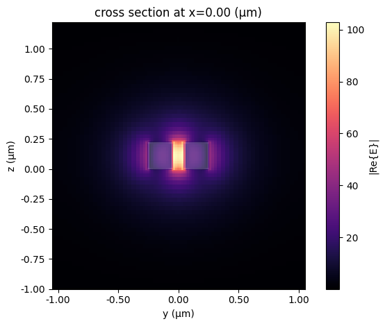
slot = pf.PortSpec(
"Slot waveguide",
width=2.1,
limits=tech.ports["Strip"].limits,
num_modes=1,
target_neff=4,
path_profiles={(2.2, 0, (1, 0)), (0.2, -0.15, (2, 0)), (0.2, 0.15, (2, 0))},
)
mode_solver = pf.port_modes(slot, freqs)
mode_solver.plot_field("E", mode_index=0, f=freqs[0], robust=False)
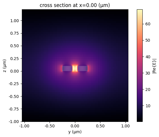
mode_solver.data.to_dataframe()
Uploading task 'Mode-ModeSolver…'
Starting task 'Mode-ModeSolver': https://tidy3d.simulation.cloud/workbench?taskId=mo-8f68b2a9-5802-43bd-82f2-20fc33f39ba5
Downloading data from 'Mode-ModeSolver'…
Progress: 100%
[5]:
| wavelength | n eff | k eff | loss (dB/cm) | TE (Ey) fraction | wg TE fraction | wg TM fraction | mode area | ||
|---|---|---|---|---|---|---|---|---|---|
| f | mode_index | ||||||||
| 1.934145e+14 | 0 | 1.55 | 1.666034 | 0.0 | 0.0 | 0.965879 | 0.869926 | 0.853944 | 0.180372 |
We can even add our new specifications to the technology, if we want to:
[6]:
tech.add_port("Strip MM", strip_mm)
tech.add_port("Slot", slot)

tech.ports
[6]:
| Name | Classification | Description | Width (μm) | Limits (μm) | Radius (μm) | Modes | Target n_eff | Path profiles (μm) | Voltage path | Current path |
|---|---|---|---|---|---|---|---|---|---|---|
| CPW | electrical | CPW transmission line | 18.7398 | -6.46388, 10.4039 | 0 | 1 | 4 | 'gnd0'@……'METAL': 6.8199 (-6.20995), 'gnd1'@'METAL': 6.8199 (+6.20995), 'signal'@'METAL': 3.6 | (2.8, 1.97) (1.8, 1.97) | (2.3, 2.72) (-2.3, 2.72) (-2.3,…… 1.22) (2.3, 1.22) |
| Rib | optical | Rib waveguide | 2.16 | -1, 1.22 | 0 | 1 | 4 | 'WG_CORE': 0.4,…… 'SLAB': 2.4, 'WG_CLAD': 2.4 | ||
| Slot | optical | Slot waveguide | 2.1 | -1, 1.22 | 0 | 1 | 4 | 'WG_CORE': 0.2…… (+0.15), 'WG_CORE': 0.2 (-0.15), 'WG_CLAD': 2.2 | ||
| Strip | optical | Strip waveguide | 2.25 | -1, 1.22 | 0 | 1 | 4 | 'WG_CORE': 0.5,…… 'WG_CLAD': 2.5 | ||
| Strip MM | optical | Multimode strip waveguide | 2.5 | -1, 1.22 | 0 | 4 | 4 | 'WG_CLAD': 2.6,…… 'WG_CORE': 0.75 |
Modifying Parametric Technologies
If a parametric technology is updated (in a Monte Carlo analysis, for example), the added port specifications will be lost. The proper way of adding a port specification to a pre-existing parametric technology is to wrap it:
[7]:
@pf.parametric_technology
def custom_basic_technology(*args, **kwargs):
    technology = pf.basic_technology(*args, **kwargs)
    slot = pf.PortSpec(
        "Slot waveguide",
        width=2.1,
        limits=tech.ports["Strip"].limits,
        num_modes=1,
        target_neff=4,
        path_profiles={(2.2, 0, (1, 0)), (0.2, -0.15, (2, 0)), (0.2, 0.15, (2, 0))},
    )
    technology.add_port("Slot", slot)
    return technology


custom_tech = custom_basic_technology()
pf.config.default_technology = custom_tech

custom_tech.ports
[7]:
| Name | Classification | Description | Width (μm) | Limits (μm) | Radius (μm) | Modes | Target n_eff | Path profiles (μm) | Voltage path | Current path |
|---|---|---|---|---|---|---|---|---|---|---|
| CPW | electrical | CPW transmission line | 18.7398 | -6.46388, 10.4039 | 0 | 1 | 4 | 'gnd0'@……'METAL': 6.8199 (-6.20995), 'gnd1'@'METAL': 6.8199 (+6.20995), 'signal'@'METAL': 3.6 | (2.8, 1.97) (1.8, 1.97) | (2.3, 2.72) (-2.3, 2.72) (-2.3,…… 1.22) (2.3, 1.22) |
| Rib | optical | Rib waveguide | 2.16 | -1, 1.22 | 0 | 1 | 4 | 'WG_CORE': 0.4,…… 'SLAB': 2.4, 'WG_CLAD': 2.4 | ||
| Slot | optical | Slot waveguide | 2.1 | -1, 1.22 | 0 | 1 | 4 | 'WG_CORE': 0.2…… (+0.15), 'WG_CORE': 0.2 (-0.15), 'WG_CLAD': 2.2 | ||
| Strip | optical | Strip waveguide | 2.25 | -1, 1.22 | 0 | 1 | 4 | 'WG_CORE': 0.5,…… 'WG_CLAD': 2.5 |
[8]:
custom_tech.update(core_thickness=0.1)

mode_solver = pf.port_modes("Slot", freqs)
mode_solver.plot_field("E", mode_index=0, f=freqs[0], robust=False)
mode_solver.data.to_dataframe()
Uploading task 'Mode-ModeSolver…'Progress: 0% -
Starting task 'Mode-ModeSolver': https://tidy3d.simulation.cloud/workbench?taskId=mo-6f28b526-09fb-4301-adf9-be19cb682266
Downloading data from 'Mode-ModeSolver'…
Progress: 100%
[8]:
| wavelength | n eff | k eff | loss (dB/cm) | TE (Ey) fraction | wg TE fraction | wg TM fraction | mode area | ||
|---|---|---|---|---|---|---|---|---|---|
| f | mode_index | ||||||||
| 1.934145e+14 | 0 | 1.55 | 1.476075 | 0.0 | 0.0 | 0.981396 | 0.952221 | 0.902956 | 0.782096 |
Waveguides
We can easily create a waveguide corresponding to a port specification using the get_paths function:
[9]:
strip = tech.ports["Slot"]

# Use a component for setting layers and visualization
connection = pf.Component("CONNECTION")

for layer, path in strip.get_paths((0, 0)):
    path.segment((5, 0)).turn(90, 4).segment((9, 6))
    connection.add(layer, path)

connection
[9]:

Adding Ports to a Component
To add a port to a component, we first need to create it by setting its position, orientation (input direction) and specification.
[10]:
port0 = pf.Port((0, 0), 0, "Slot")

# Set the port name to "P0"
connection.add_port(port0, "P0")

connection
[10]:

Another option is to use port auto-detection to look for possible ports in the component.
Auto-detection works by matching the required path profiled in the port specifications to the edges in the component geometry, which means:
There can be false positives if a port profile is very simple and it matches several edges in the component geometry.

Ports will not be found if, for example, a clad layer is required to surround the waveguide core, but only the core edge is found

[11]:
detected_ports = connection.detect_ports(["Slot"])
detected_ports
[11]:
[Port(center=(9, 6), input_direction=270, spec=PortSpec(description="Slot waveguide", width=2.1, limits=(-1, 1.22), num_modes=1, added_solver_modes=0, polarization="", target_neff=4, default_radius=0, path_profiles=[(0.2, 0.15, (2, 0)), (0.2, -0.15, (2, 0)), (2.2, 0, (1, 0))]), extended=True, inverted=False, bend_radius=0)]
Note that the auto-detection skipped the port at (0, 0) because it was already present in the component (it does not create duplicates).
[12]:
connection.add_port(detected_ports[0], "P1")
connection
[12]:
