
Inverse Designed Grating Coupler

In this notebook, we demonstrate fabrication-aware inverse design using PhotonForge together with Tidy3D’s inverse design framework.
PhotonForge is an end-to-end photonic design automation platform that accelerates photonic integrated circuit development by seamlessly integrating simulation tools, layout editing, circuit-level system modeling, and foundry PDKs into one unified workflow. Tidy3D’s inverse design framework computes the derivative of a figure of merit (such as transmission) with respect to any number of design parameters using the adjoint method, at the cost of a single additional simulation.
Since version 1.4.4, PhotonForge integrates this capability natively: we describe the device as a parametric component, and PhotonForge automatically generates the Tidy3D simulation from the technology stack and differentiates its S matrix through the adjoint solver. No manual simulation management is required (see the Inverse Design with Autograd guide). Because the geometry gradients are computed for the structures inside the simulation, the ports and the simulation domain are kept independent of the optimized parameters.
In this example, we optimize a grating coupler. The initial structure is based on this PhotonForge example, which follows the design presented in [1]. The simulations are run in two dimensions to keep the optimization fast.
For additional examples of inverse-designed grating couplers, see this and this Tidy3D notebook. For a broader overview of inverse design in Tidy3D, refer to the Inverse Design Quickstart.
References
Frederik Van Laere, Tom Claes, Jonathan Schrauwen, Stijn Scheerlinck, Wim Bogaerts, Dirk Taillaert, Liam O’Faolain, Dries Van Thourhout, Roel Baets, “Compact Focusing Grating Couplers for Silicon-on-Insulator Integrated Circuits,” IEEE Photonics Technology Letters, 2007 19 (23), 1919–1921, doi: 10.1109/LPT.2007.908762
The general workflow for this notebook is summarized below. Unlike a manual adjoint setup, PhotonForge builds the differentiable Tidy3D simulation directly from the parametric component, so there is no separate base-simulation export or structure-injection step.

[1]:
import autograd as ag
import autograd.numpy as np  # Important to import autograd's numpy module for tracing derivatives
import optax
import photonforge as pf
import tidy3d as td
from matplotlib import pyplot as plt

# We raise the Tidy3D logging level to reduce output noise during the
# optimization loop. Warnings can flag real problems, so only suppress them
# once you have confirmed they are not relevant to your case.
td.config.logging.level = "ERROR"
# Set the default PhotonForge -> Tidy3D mesh refinement
# We are running 2D simulations, so this can be set rather high
pf.config.default_mesh_refinement = 30.0
Technology Setup
In the first part of this notebook, we set up the technology stack.
The technology used in the reference work [1] is similar to PhotonForge’s basic technology, with two key differences: the slab thickness and the absence of the top cladding.
To emulate the 70 nm etch depth from the reference design, we set the slab_thickness to 150 nm:
[2]:
tech = pf.basic_technology(slab_thickness=0.15)
pf.config.default_technology = tech
We can view the layers and extrusions provided by the technology
[3]:
tech.layers
[3]:
| Name | Layer | Description | Color | Pattern |
|---|---|---|---|---|
| WG_CLAD | (1, 0) | Waveguide clad | #9da6a218 | . |
| WG_CORE | (2, 0) | Waveguide core | #6db5dd18 | / |
| SLAB | (3, 0) | Slab region | #8851ad18 | : |
| TRENCH | (4, 0) | Deep-etched trench for chip…… facets | #535e5918 | + |
| METAL | (5, 0) | Metal layer | #b8a18b18 | \ |
[4]:
tech.extrusion_specs
[4]:
| # | Mask | Limits (μm) | Sidewal (°) | Opt. Medium | Elec. Medium |
|---|---|---|---|---|---|
| 0 | () | -inf, 0 | 0 | cSi_Li1993_293K | Medium(permittivity=12.3) |
| 1 | () | -2, 1.72 | 0 | SiO2_Palik_LowLoss | Medium(permittivity=4.2) |
| 2 | 'WG_CORE' | 0, 0.22 | 0 | cSi_Li1993_293K | Medium(permittivity=12.3) |
| 3 | 'SLAB' | 0, 0.15 | 0 | cSi_Li1993_293K | Medium(permittivity=12.3) |
| 4 | 'METAL' | 1.72, 2.22 | 0 | Cu_JohnsonChristy1972 | PEC |
| 5 | 'TRENCH' | -inf, inf | 0 | Medium() | Medium() |
Unfortunately, there is no direct argument to remove the top cladding in the basic technology, because both the top and bottom media are defined by the background medium. Additionally, setting the top cladding thickness to zero is not an option, since it is used internally to define the port dimensions.
A better approach is to add a new extrusion specification to the technology. This specification will create an extra air volume above the substrate with infinite vertical extent. We can achieve this using the insert_extrusion_spec method:
[5]:
# An empty mask covers the whole device bounds
air_extrusion = pf.ExtrusionSpec(
    pf.MaskSpec(), td.Medium(permittivity=1.0, name="air"), limits=(0, pf.Z_INF)
)

# Insert air volume first, so that all core extrusions override the air clad
tech.insert_extrusion_spec(0, air_extrusion)

# Print the updated extrusion specs
tech.extrusion_specs
[5]:
| # | Mask | Limits (μm) | Sidewal (°) | Opt. Medium | Elec. Medium |
|---|---|---|---|---|---|
| 0 | () | 0, inf | 0 | air | air |
| 1 | () | -inf, 0 | 0 | cSi_Li1993_293K | Medium(permittivity=12.3) |
| 2 | () | -2, 1.72 | 0 | SiO2_Palik_LowLoss | Medium(permittivity=4.2) |
| 3 | 'WG_CORE' | 0, 0.22 | 0 | cSi_Li1993_293K | Medium(permittivity=12.3) |
| 4 | 'SLAB' | 0, 0.15 | 0 | cSi_Li1993_293K | Medium(permittivity=12.3) |
| 5 | 'METAL' | 1.72, 2.22 | 0 | Cu_JohnsonChristy1972 | PEC |
| 6 | 'TRENCH' | -inf, inf | 0 | Medium() | Medium() |
Parametric Grating Coupler
We define the entire grating coupler as a single parametric component. PhotonForge automatically generates the Tidy3D simulation from the technology stack: the partial etch is realized simply by drawing the etched sections on the slab layer, with the extrusion specifications taking care of all vertical bounds. The component also carries its two ports — the Gaussian port is converted to a Gaussian source and the waveguide port to a mode monitor when the simulation is generated — and a Tidy3D model.
Because the function is a parametric component, it is automatically differentiable: when called with parameters traced by Autograd (here, the arrays of grating gaps and tooth widths), it returns a differentiable version of the component whose s_matrix supports gradient computation. Gradients are computed for the structures inside the simulation, so the ports and the simulation domain must not depend on the traced parameters: the fiber position is a separate (non-traced) argument, and the
simulation bounds are pinned through the model — which also makes the simulation two dimensional by collapsing the y axis.
Below are the setup parameters for the component.
Note: Since we are working in 2D, the waveguide width is arbitrary.
[6]:
# Setup parameters
wg_width = 6  # This is arbitrary because the simulation is 2D
wg_length = 30
fiber_angle = 10
fiber_translation = 3
waist_radius = 6.0
gaussian_port_height = 0.5

# Define the gaussian port input vector based on the fiber angle
sin_angle = np.sin(fiber_angle / 180 * np.pi)
cos_angle = np.cos(fiber_angle / 180 * np.pi)
input_vector = (-sin_angle, 0, -cos_angle)
[7]:
period = 0.63        # Grating period in microns
gc_len = 15.5        # Total grating length in microns
ncells = int(round(gc_len / period))  # Number of grating periods
fill_factor = 0.5    # Filling factor at each period

# Initial grating structure: uniform fill factor
gc_widths = np.ones(shape=ncells) * period * fill_factor
gc_gaps = period - gc_widths
gc_startx = 5.0  # x-coordinate where the grating starts
[8]:
input_wg_portspec = pf.PortSpec(
    "input wg",
    width=wg_width,
    limits=tech.ports["Strip"].limits,
    num_modes=1,
    target_neff=3.5,
    path_profiles={(wg_width, 0, tech.layers["WG_CORE"].layer)},
)
[9]:
@pf.parametric_component
def grating_coupler(*, gc_gaps, gc_widths, fiber_position=wg_length / 2 + fiber_translation):
    c = pf.Component("GC")

    # Grating teeth (unetched core islands) generated by the apodized-grating helper
    teeth = pf.stencil.apodized_grating(
        teeth_gaps=gc_gaps,
        teeth_widths=gc_widths,
        width=wg_width,
        taper_length=0,
        taper_width=wg_width,
    )
    for tooth in teeth:
        tooth.translate((gc_startx, 0))
    c.add("WG_CORE", *teeth)

    # Input waveguide and the partially-etched slab spanning the grating region.
    # The teeth sit on the 220 nm core; the surrounding slab is etched down to
    # 150 nm, and the region after the last tooth is fully etched.
    c.add("WG_CORE", pf.Rectangle((0, -wg_width / 2), (gc_startx, wg_width / 2)))
    grating_length = float(np.sum(gc_gaps) + np.sum(gc_widths))
    c.add("SLAB", pf.Rectangle((gc_startx, -wg_width / 2), (gc_startx + grating_length, wg_width / 2)))

    # Waveguide port (mode monitor) and Gaussian port (source)
    c.add_port(pf.Port((0, 0), 0, input_wg_portspec))
    c.add_port(
        pf.GaussianPort(
            (fiber_position, 0, gaussian_port_height),
            input_vector,
            waist_radius,
            polarization_angle=90,
            field_tolerance=1e-2,
        )
    )

    # The y bounds collapse the simulation to 2D and the fixed x bound keeps the
    # simulation domain independent of the traced grating geometry
    c.add_model(
        pf.Tidy3DModel(
            verbose=False,
            bounds=((None, 0, None), (wg_length, 0, None)),
            boundary_spec=td.BoundarySpec(
                x=td.Boundary.absorber(),
                y=td.Boundary.periodic(),
                z=td.Boundary.absorber(),
            ),
        ),
        "Tidy3D",
    )
    return c
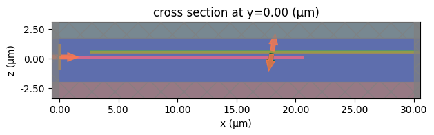
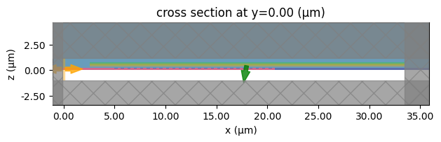
PhotonForge generates one simulation for each source port. We select the simulation labeled "P1@0", which corresponds to port P1 (the Gaussian port) being used as the excitation source, and visualize it to check the setup: the background structures from the technology stack, the grating teeth, the Gaussian beam source (green), and the waveguide mode monitor (orange) are all generated automatically.
[10]:
wavelengths = np.linspace(1.5, 1.6, 21)

gc = grating_coupler(gc_gaps=gc_gaps, gc_widths=gc_widths)
sims = gc.models["Tidy3D"].get_simulations(gc, pf.C_0 / wavelengths)
sims["P1@0"].plot(y=0)
plt.show()
The source position is likely not optimal for high coupling efficiency, but we can compute the S matrix to ensure there are no setup errors. Note that we restrict the computation to the Gaussian port excitation through the inputs argument, since the transmission towards the fiber follows from reciprocity.
[11]:
s_matrix = gc.s_matrix(pf.C_0 / wavelengths, model_kwargs={"inputs": ["P1"]})
transmission = np.abs(s_matrix["P1@0", "P0@0"]) ** 2

f, ax = plt.subplots()
ax.plot(wavelengths, transmission)
ax.set_xlabel("wavelength (µm)")
ax.set_ylabel("transmission")
ax.grid()
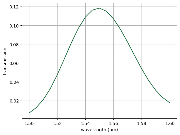
The initial simulation looks correct.
Now let’s sweep the fiber position and find the position for the best coupling. Each position is a regular (non-traced) component evaluation at the center wavelength.
[12]:
# Sweep the fiber position for best coupling at the center wavelength
centerwl = 1.55
fiber_pos = np.linspace(5, 15, 11)

T_centerwl = []
for fpos in fiber_pos:
    gc_swept = grating_coupler(gc_gaps=gc_gaps, gc_widths=gc_widths, fiber_position=fpos)
    s = gc_swept.s_matrix(
        [pf.C_0 / centerwl], show_progress=False, model_kwargs={"inputs": ["P1"]}
    )
    T_centerwl.append(np.abs(s["P1@0", "P0@0"][0]) ** 2)
[13]:
f, ax = plt.subplots()
ax.plot(fiber_pos, T_centerwl, "-o")
ax.set_xlabel("fiber source position (um)")
ax.set_ylabel(f"transmission at {centerwl} wavelength")
ax.grid()
plt.show()
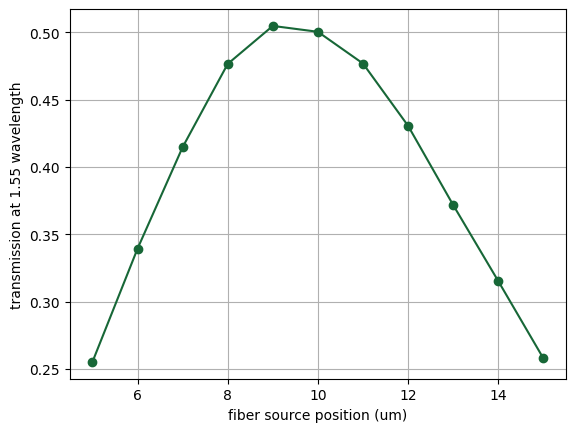
It looks like a good source position is around 9 µm. We keep this position fixed for the adjoint optimization.
[14]:
best_fiber_pos = fiber_pos[np.argmax(T_centerwl)]
print(f"Best fiber position: {best_fiber_pos} µm")
Best fiber position: 9.0 µm
Adjoint Optimization
We start by defining an objective function to optimize: the transmission at the center wavelength. The grating response is smooth, single-frequency gradients require a single adjoint simulation, and the result files stay small because only one frequency of volumetric field data is involved — the full band is verified after the optimization. (The original version of this example optimized the worst case across a 10 nm band; that requires a differentiable minimum across the per-frequency values and twice the adjoint cost.)
The objective function receives the optimization parameters as a single flat array — the grating gaps followed by the tooth widths — and slices it directly into the two traced array arguments of the parametric component. No conversion helpers or manual simulation management are needed: the s_matrix call on the traced component runs the forward simulation and registers the adjoint computation automatically — one forward and one adjoint simulation per gradient evaluation, independently of the
number of parameters.
[15]:
# The center frequency to optimize for
centerfreq = pf.C_0 / centerwl


def objective(params_array):
    gaps = params_array[:ncells]
    widths = params_array[ncells:]

    gc = grating_coupler(gc_gaps=gaps, gc_widths=widths, fiber_position=best_fiber_pos)
    s = gc.s_matrix([centerfreq], show_progress=False, model_kwargs={"inputs": ["P1"]})

    return np.abs(s["P1@0", "P0@0"][0]) ** 2
In a real photonic integrated circuit (PIC) platform, there are minimum feature size constraints. These include:
Minimum line width: the smallest allowable feature width (e.g., for etched or deposited material).
Minimum space (gap): the smallest allowable spacing between features.
We define these constraints and enforce them inside the optimization loop using parameter clipping. Clipping ensures that no design parameter violates the minimum line or gap rules.
[16]:
min_line = 0.15
min_space = 0.2

# Minimum values for each entry of the flat parameter array (gaps, then widths)
minfeatarr = np.concatenate((min_space * np.ones(ncells), min_line * np.ones(ncells)))
Now we assemble the various components into the main optimization loop.
In addition to the starting design and objective function, we also define hyperparameters such as the number of optimization steps, learning rate, and the optimizer. We use the Adam algorithm from the Optax package, which is well-suited for gradient-based optimization.
PhotonForge’s native autograd support evaluates the gradients through Tidy3D’s adjoint solver via the chain rule through general Python code. The optimizer then updates the parameters at each step using these gradients.
[17]:
# Optimization parameters
learning_rate = 1e-2
num_steps = 40

# The starting design as a single flat parameter array
params_array = np.concatenate((gc_gaps, gc_widths))

# Initialize the optimizer with starting parameters
optimizer = optax.adam(learning_rate=learning_rate)
opt_state = optimizer.init(params_array)

# Arrays that store the optimization history
objective_history = []
param_history = [params_array]
gradient_history = []

# To use Autograd to calculate the gradient of our objective function, we wrap it within
# Autograd's value_and_grad() function.
grad_fn = ag.value_and_grad(objective)
We now run the optimization for 40 iterations with a learning rate of 1e-2, targeting the center wavelength of 1550 nm. Feel free to experiment with the learning rate, step count, or target wavelength based on your application.
[18]:
for ii in range(num_steps):
    print(f"step = {ii + 1}")

    # Evaluate the current value and gradient of our objective function with the current parameters.
    value, gradient = grad_fn(params_array)

    # Print the outputs
    print(f"\tJ = {value:.4e}")
    print(f"\tgrad_norm = {np.linalg.norm(gradient):.4e}")

    # Compute and apply updates to the parameters based on the computed gradient.
    # The Optax Adam optimizer is used to compute and apply the updates.
    # Note that the gradient is negated for maximizing the objective (the default behavior is to minimize).
    updates, opt_state = optimizer.update(-gradient, opt_state, params_array)
    params_array = optax.apply_updates(params_array, updates)
    params_array = np.array(params_array)

    # Enforce DRC constraints by clipping the parameters.
    np.clip(params_array, minfeatarr, None, out=params_array)

    # Save the results of this iteration step to the history.
    objective_history.append(value)
    param_history.append(params_array)
    gradient_history.append(gradient)
step = 1
        J = 5.0498e-01
        grad_norm = 4.0320e+00
step = 2
        J = 3.5794e-01
        grad_norm = 6.5418e+00
step = 3
        J = 4.6010e-01
        grad_norm = 4.7320e+00
step = 4
        J = 5.4008e-01
        grad_norm = 1.3257e+00
step = 5
        J = 4.8658e-01
        grad_norm = 4.5695e+00
step = 6
        J = 4.8574e-01
        grad_norm = 4.4505e+00
step = 7
        J = 5.2144e-01
        grad_norm = 2.3670e+00
step = 8
        J = 5.1468e-01
        grad_norm = 1.2352e+00
step = 9
        J = 4.7572e-01
        grad_norm = 3.1450e+00
step = 10
        J = 4.6826e-01
        grad_norm = 3.4605e+00
step = 11
        J = 4.9586e-01
        grad_norm = 2.3169e+00
step = 12
        J = 5.2376e-01
        grad_norm = 4.4102e-01
step = 13
        J = 5.2097e-01
        grad_norm = 2.1826e+00
step = 14
        J = 5.0953e-01
        grad_norm = 3.1348e+00
step = 15
        J = 5.1832e-01
        grad_norm = 2.6297e+00
step = 16
        J = 5.3024e-01
        grad_norm = 8.7412e-01
step = 17
        J = 5.2314e-01
        grad_norm = 1.0783e+00
step = 18
        J = 5.0935e-01
        grad_norm = 2.1889e+00
step = 19
        J = 5.0794e-01
        grad_norm = 2.3473e+00
step = 20
        J = 5.2059e-01
        grad_norm = 1.5403e+00
step = 21
        J = 5.3179e-01
        grad_norm = 2.3669e-01
step = 22
        J = 5.2948e-01
        grad_norm = 1.5115e+00
step = 23
        J = 5.2604e-01
        grad_norm = 1.9669e+00
step = 24
        J = 5.3001e-01
        grad_norm = 1.4851e+00
step = 25
        J = 5.3196e-01
        grad_norm = 2.2857e-01
step = 26
        J = 5.2465e-01
        grad_norm = 1.0777e+00
step = 27
        J = 5.1901e-01
        grad_norm = 1.5764e+00
step = 28
        J = 5.2293e-01
        grad_norm = 1.2308e+00
step = 29
        J = 5.2931e-01
        grad_norm = 2.1586e-01
step = 30
        J = 5.2972e-01
        grad_norm = 7.5756e-01
step = 31
        J = 5.2836e-01
        grad_norm = 1.0957e+00
step = 32
        J = 5.2853e-01
        grad_norm = 9.5172e-01
step = 33
        J = 5.2892e-01
        grad_norm = 4.3183e-01
step = 34
        J = 5.2707e-01
        grad_norm = 3.2144e-01
step = 35
        J = 5.2370e-01
        grad_norm = 8.5927e-01
step = 36
        J = 5.2266e-01
        grad_norm = 9.7338e-01
step = 37
        J = 5.2533e-01
        grad_norm = 5.1825e-01
step = 38
        J = 5.2749e-01
        grad_norm = 2.4974e-01
step = 39
        J = 5.2703e-01
        grad_norm = 7.5494e-01
step = 40
        J = 5.2593e-01
        grad_norm = 8.3397e-01
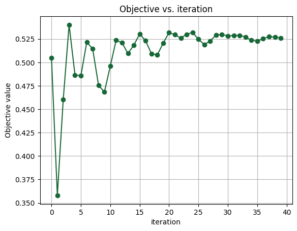
Once the optimization is complete we can view the results:
[19]:
# Plot the objective value versus iteration.
f, ax = plt.subplots()
ax.plot(objective_history, "-o")
ax.set_xlabel("iteration")
ax.set_ylabel("Objective value")
ax.grid()
ax.set_title("Objective vs. iteration")
# Select the best design parameters.
best_params = param_history[np.argmax(objective_history)]
best_gaps = best_params[:ncells]
best_widths = best_params[ncells:]
# Compare the starting and final params.
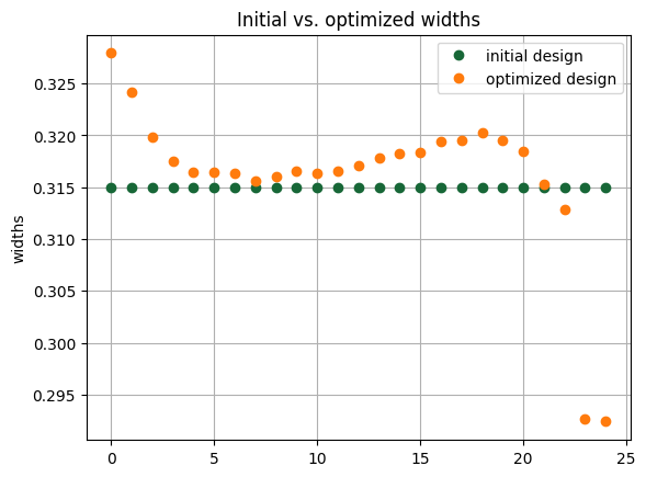
f, ax = plt.subplots()
ax.plot(gc_widths, "o", label="initial design")
ax.plot(best_widths, "o", label="optimized design")
ax.set_ylabel("widths")
ax.grid()
ax.legend()
ax.set_title("Initial vs. optimized widths")
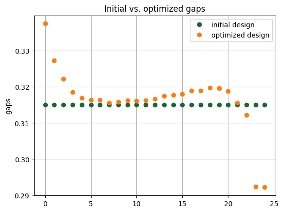
f, ax = plt.subplots()
ax.plot(gc_gaps, "o", label="initial design")
ax.plot(best_gaps, "o", label="optimized design")
ax.set_ylabel("gaps")
ax.grid()
ax.legend()
ax.set_title("Initial vs. optimized gaps")
plt.show()
Finally, we can simulate the optimized design, and compare it with the initial design.
[20]:
gc_start = grating_coupler(
    gc_gaps=gc_gaps, gc_widths=gc_widths, fiber_position=best_fiber_pos
)
gc_best = grating_coupler(
    gc_gaps=best_gaps, gc_widths=best_widths, fiber_position=best_fiber_pos
)

s_start = gc_start.s_matrix(pf.C_0 / wavelengths, model_kwargs={"inputs": ["P1"]})
s_best = gc_best.s_matrix(pf.C_0 / wavelengths, model_kwargs={"inputs": ["P1"]})
[21]:
# Plot final transmission, compare to the initial design
T_startdesign = np.abs(s_start["P1@0", "P0@0"]) ** 2
T_bestdesign = np.abs(s_best["P1@0", "P0@0"]) ** 2

f, ax = plt.subplots()
ax.plot(wavelengths, T_startdesign, label="initial design")
ax.plot(wavelengths, T_bestdesign, label="optimized design")
ax.set_xlabel("wavelength (um)")
ax.set_ylabel("transmission")
ax.grid()
ax.legend()

plt.show()
We can see that the final design has centered the transmission spectrum on our design wavelength, and slightly improved the coupling efficiency. More improvement could be possible by experimenting with the optimization hyperparameters, such as the starting design or the coupling bandwidth. Feel free to experiment if you would like and see if you can improve the design even more.