
Analytic Ring Resonator Model

The RingModel provides a compact, physically meaningful description of ring resonators and microring modulators in frequency domain. It captures the full resonator physics - coupling, round-trip phase and loss, dispersion, temperature tuning, and electro-optic modulation - in a single component model.
Feature |
Parameters |
|---|---|
Bus coupling |
\(\kappa_1\), \(\kappa_2\) (field coupling coefficients) |
Round-trip phase |
\(n_\text{eff}\), \(L\) (ring circumference) |
Dispersion |
\(n_\text{group}\), \(D\) (chromatic dispersion), \(S\) (dispersion slope) |
Loss |
\(L_p\) (propagation loss per unit length) |
Thermal tuning |
\(\mathrm{d}n/\mathrm{d}T\), \(\mathrm{d}L_p/\mathrm{d}T\) |
EO modulation |
\(\mathrm{d}n/\mathrm{d}V\), \(\mathrm{d}^2n/\mathrm{d}V^2\), \(\mathrm{d}L_p/\mathrm{d}V\), \(\mathrm{d}^2L_p/\mathrm{d}V^2\) |
All-pass ring (single bus)
When only kappa1 is provided (kappa2=None), the model describes an all-pass ring with one input port and one through port. The through-port field transmission is:
where \(\tau_1 = \sqrt{1 - |\kappa_1|^2}\) is the self-coupling (transmission) coefficient, \(a = 10^{-L_p L / 20}\) is the round-trip field transmission amplitude, and \(\phi = 2\pi n_\text{eff} L f / c_0\) is the round-trip phase.
Add-drop ring (double bus)
When kappa2 is also set, the model adds a second bus to form an add-drop ring with four ports (in, through, drop, add). The drop-port transmission is:
This notebook walks through each parameter, building physical intuition with black_box_component before showing a practical ring modulator example.
Setup
[1]:
import matplotlib.pyplot as plt
import numpy as np
import photonforge as pf
[2]:
tech = pf.basic_technology()
pf.config.default_technology = tech

# n_eff chosen so that m = n_eff * L / lambda0 is an integer at lambda0 = 1.55 µm
# With L = 50 µm and m = 78:  n_eff = 78 * 1.55 / 50 = 2.418  → resonance at exactly 1550 nm
n_eff_ring = 78 * 1.55 / 50   # 2.418
n_group_ring = 4.2
L_ring = 50.0  # µm round-trip circumference

# FSR ≈ lambda² / (n_group * L) ≈ 11.4 nm  →  show ~2 FSRs in the broad window
wavelengths = np.linspace(1.535, 1.565, 30001)
freqs = pf.C_0 / wavelengths
f0 = pf.C_0 / 1.55  # reference frequency at 1550 nm

# Zoomed window: one resonance at 1550 nm
wavelengths_zoom = np.linspace(1.547, 1.553, 2001)
freqs_zoom = pf.C_0 / wavelengths_zoom
Basic All-Pass Ring
The minimum required parameters are kappa1, n_eff, and length. We also add a small propagation_loss from the start: a lossless all-pass ring has unit magnitude transmission at every wavelength (energy conservation), so the resonances only appear in the phase spectrum, not the power spectrum.
Round-trip resonance condition: The ring resonates when the round-trip phase is a multiple of \(2\pi\):
To place a resonance at exactly \(\lambda_0 = 1550\) nm with \(L = 50\,\mu\)m we need \(n_\text{eff} = m\,\lambda_0 / L\) to be an integer multiple of \(\lambda_0/L = 0.031\). Using \(m = 78\) gives \(n_\text{eff} = 2.418\).
Free spectral range: The spacing between adjacent resonances is controlled by the group index:
Coupling coefficient \(\kappa_1\): The fraction of power entering the ring per pass is \(|\kappa_1|^2\). The model computes the self-coupling coefficient as \(\tau_1 = -i\,e^{i\,\angle\kappa_1}\sqrt{1-|\kappa_1|^2}\). Use \(\kappa_1 = +i\,|\kappa_1|\) to get a positive-real \(\tau_1\), which is the convention that places the resonance at \(\phi = 2\pi m\) (i.e., at the design wavelength). Using \(-i\,|\kappa_1|\) shifts the resonance by half an FSR.
[3]:
ring_basic = pf.RingModel(
    kappa1=1j * 0.2,          # |kappa1|^2 = 0.04; +1j gives positive-real tau1 -> resonance at design wavelength
    n_eff=n_eff_ring,          # 2.418: resonance at exactly 1550 nm
    n_group=n_group_ring,      # 4.2:  sets FSR ~ 11.4 nm
    length=L_ring,             # 50 um round-trip
    propagation_loss=2e-3,    # dB/um, needed to make resonance dips visible
    reference_frequency=f0,
)

bb_basic = ring_basic.black_box_component(port_spec="Strip")
bb_basic
[3]:

[4]:
s_basic = bb_basic.s_matrix(freqs, show_progress=False)
thru_key = ("P0@0", "P1@0")

fig, axes = plt.subplots(1, 2, figsize=(12, 4))

axes[0].plot(wavelengths, np.abs(s_basic[thru_key]) ** 2)
axes[0].set_xlabel("Wavelength (µm)")
axes[0].set_ylabel("Through-port power $|t_1|^2$")
axes[0].set_title("All-pass ring - through port spectrum")

axes[1].plot(wavelengths, np.unwrap(np.angle(s_basic[thru_key])))
axes[1].set_xlabel("Wavelength (µm)")
axes[1].set_ylabel("Phase (rad)")
axes[1].set_title("Through-port phase")

fig.tight_layout()
plt.show()
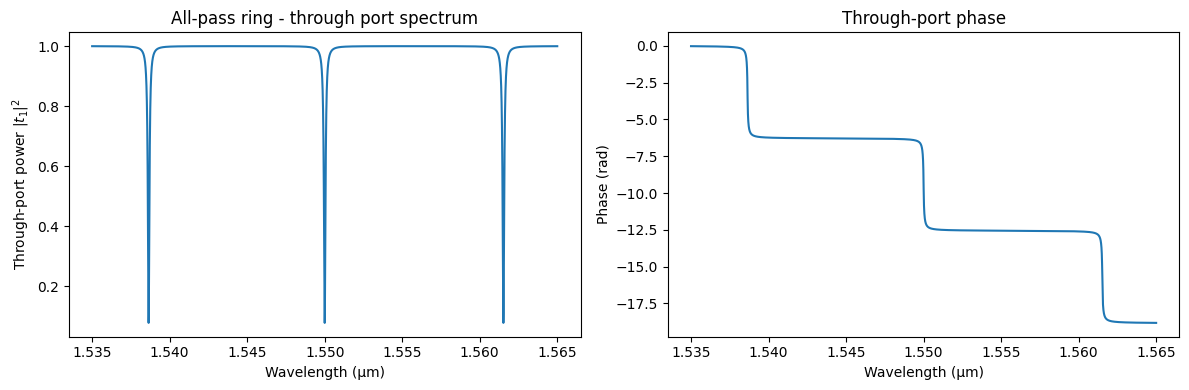
At resonance the circulating field builds up inside the ring and leaks back to the bus in antiphase with the direct transmission, creating the characteristic notch. The resonance at 1550 nm and its neighbour at 1550 − FSR ≈ 1538.6 nm are both visible in the broad wavelength window.
Coupling Coefficient and Lineshape
The coupling coefficient kappa1 has both a magnitude and a phase:
\(|\kappa_1|^2\) is the power fraction coupled from the bus into the ring per pass.
The phase of \(\kappa_1\) sets the coupler convention. Use \(\kappa_1 = +i\,|\kappa_1|\) (positive imaginary) to obtain a positive-real self-coupling \(\tau_1\), which places the resonance at the design wavelength.
The lineshape depends on the ratio of coupling to round-trip loss:
Regime |
Condition |
Observation |
|---|---|---|
Under-coupled |
\(|\kappa_1|^2 < 1 - a^2\) |
Shallow notch, narrow linewidth |
Critically coupled |
\(|\kappa_1|^2 = 1 - a^2\) |
Perfect null at resonance |
Over-coupled |
\(|\kappa_1|^2 > 1 - a^2\) |
Deep but broad notch |
where \(a = 10^{-L_p L/20}\) is the round-trip field transmission.
Below we fix the round-trip loss and sweep the coupling strength to see these three regimes.
[5]:
L_p = 2e-3   # dB/um
a = 10 ** (-(L_p * L_ring) / 20)
kappa_crit = np.sqrt(1 - a**2)

print(f"Round-trip power loss: {L_p * L_ring:.2f} dB  ->  field amplitude a = {a:.4f}")
print(f"Critical coupling: |kappa_crit|^2 = {kappa_crit**2:.4f}  ->  |kappa_crit| = {kappa_crit:.4f}")

fig, axes = plt.subplots(1, 2, figsize=(12, 4))

cases = [
    (kappa_crit * 0.4,  "Under-coupled ($|\\kappa|^2 = 0.4\\,|\\kappa_c|^2$)"),
    (kappa_crit,        "Critically coupled ($|\\kappa|^2 = |\\kappa_c|^2$)"),
    (kappa_crit * 2.0,  "Over-coupled ($|\\kappa|^2 = 4\\,|\\kappa_c|^2$)"),
]

for kappa_mag, label in cases:
    kappa_mag = min(kappa_mag, 0.9999)
    m = pf.RingModel(
        kappa1=1j * kappa_mag,
        n_eff=n_eff_ring,
        n_group=n_group_ring,
        length=L_ring,
        propagation_loss=L_p,
        reference_frequency=f0,
    )
    bb = m.black_box_component(port_spec="Strip")
    s = bb.s_matrix(freqs_zoom, show_progress=False)
    T = np.abs(s[thru_key]) ** 2
    axes[0].plot(wavelengths_zoom * 1e3, T, label=label)
    axes[1].plot(wavelengths_zoom * 1e3, 10 * np.log10(T + 1e-30), label=label)

axes[0].set_xlabel("Wavelength (nm)")
axes[0].set_ylabel("Through-port power")
axes[0].set_title("Coupling regime: linear scale")
axes[0].legend(fontsize=8)

axes[1].set_xlabel("Wavelength (nm)")
axes[1].set_ylabel("Through-port power (dB)")
axes[1].set_title("Coupling regime: log scale")
axes[1].set_ylim(-50, 1)
axes[1].legend(fontsize=8)

fig.tight_layout()
plt.show()
Round-trip power loss: 0.10 dB  ->  field amplitude a = 0.9886
Critical coupling: |kappa_crit|^2 = 0.0228  ->  |kappa_crit| = 0.1509
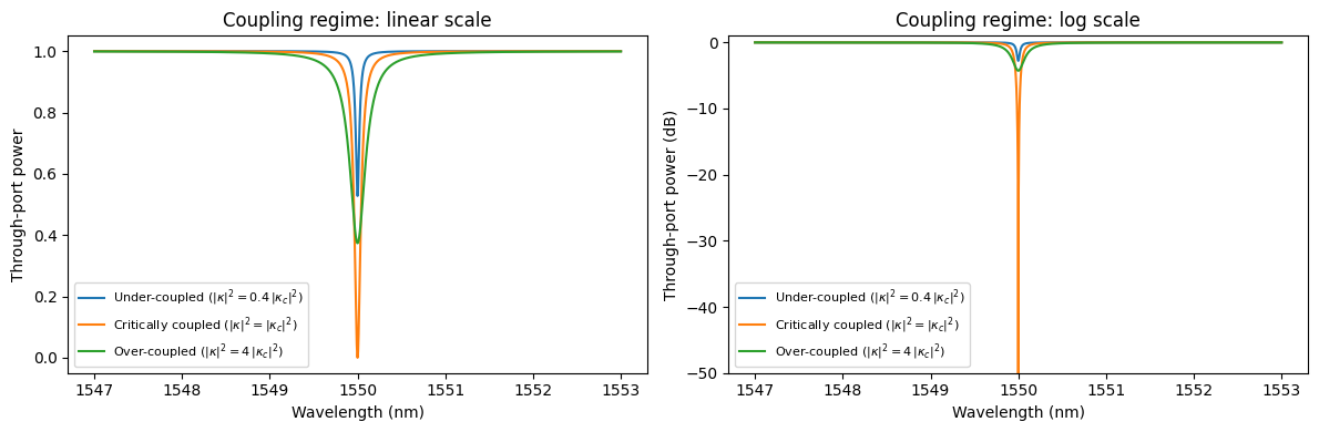
Critical coupling is the sweet spot where the coupling loss exactly cancels the round-trip loss, creating a perfect null. Over-coupling broadens the resonance and increases the 3-dB bandwidth - useful for modulators where a large electro-optic bandwidth is desired at the cost of reduced extinction.
Round-trip Loss and Quality Factor
The propagation_loss parameter sets the waveguide loss in dB/µm. The key derived quantities are:
Loaded Q factor: \(Q = \pi n_g L f_0 / (c_0 \cdot \delta f_{FWHM})\) - the ratio of resonance frequency to linewidth.
Photon lifetime: \(\tau_\text{ph} = Q / (2\pi f_0)\)
Finesse: \(\mathcal{F} = \text{FSR} / \delta f_{FWHM}\)
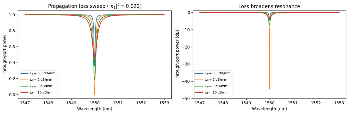
Higher propagation loss broadens the resonance (lower Q). Below we sweep the loss at fixed coupling and observe how it degrades the extinction ratio and broadens the linewidth.
[6]:
fig, axes = plt.subplots(1, 2, figsize=(12, 4))

kappa_fixed = 0.15
losses = [0.5e-3, 2e-3, 5e-3, 10e-3]
labels = ["$L_p = 0.5$ dB/mm", "$L_p = 2$ dB/mm", "$L_p = 5$ dB/mm", "$L_p = 10$ dB/mm"]

for L_p_val, label in zip(losses, labels):
    m = pf.RingModel(
        kappa1=1j * kappa_fixed,
        n_eff=n_eff_ring,
        n_group=n_group_ring,
        length=L_ring,
        propagation_loss=L_p_val,
        reference_frequency=f0,
    )
    bb = m.black_box_component(port_spec="Strip")
    s = bb.s_matrix(freqs_zoom, show_progress=False)
    T = np.abs(s[thru_key]) ** 2
    axes[0].plot(wavelengths_zoom * 1e3, T, label=label)
    axes[1].plot(wavelengths_zoom * 1e3, 10 * np.log10(T + 1e-30), label=label)

axes[0].set_xlabel("Wavelength (nm)")
axes[0].set_ylabel("Through-port power")
axes[0].set_title(f"Propagation loss sweep ($|\\kappa_1|^2 = {kappa_fixed**2:.3f}$)")
axes[0].legend(fontsize=8)

axes[1].set_xlabel("Wavelength (nm)")
axes[1].set_ylabel("Through-port power (dB)")
axes[1].set_ylim(-50, 1)
axes[1].set_title("Loss broadens resonance")
axes[1].legend(fontsize=8)

fig.tight_layout()
plt.show()
Ring Length and Free Spectral Range
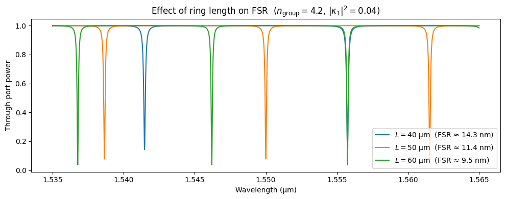
The length parameter is the full round-trip circumference. Doubling the length halves the FSR: resonances pack twice as closely. The FSR also depends on the group index, not the effective index.
[7]:
fig, ax = plt.subplots(figsize=(10, 4))

for length in [40, 50, 60]:
    fsr_nm = (1.55e-6) ** 2 / (n_group_ring * length * 1e-6) * 1e9
    m = pf.RingModel(
        kappa1=1j * 0.2,
        n_eff=n_eff_ring,
        n_group=n_group_ring,
        length=length,
        propagation_loss=2e-3,
        reference_frequency=f0,
    )
    bb = m.black_box_component(port_spec="Strip")
    s = bb.s_matrix(freqs, show_progress=False)
    ax.plot(wavelengths, np.abs(s[thru_key]) ** 2,
            label=f"$L = {length}$ µm  (FSR ≈ {fsr_nm:.1f} nm)")

ax.set_xlabel("Wavelength (µm)")
ax.set_ylabel("Through-port power")
ax.set_title("Effect of ring length on FSR  ($n_\\mathrm{group} = 4.2$, $|\\kappa_1|^2 = 0.04$)")
ax.legend()
fig.tight_layout()
plt.show()
Effective Index vs. Group Index
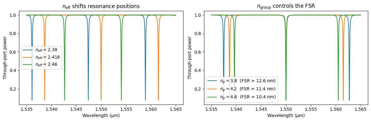
n_effsets the resonance wavelength positions via \(\lambda_m = n_\text{eff} L / m\).n_groupsets the FSR (spacing between resonances) via FSR ≈ \(\lambda^2 / (n_g L)\).
In silicon photonics \(n_\text{eff} \approx 2.4\) and \(n_\text{group} \approx 4.2\) for a 500 nm strip waveguide at 1550 nm. Changing n_eff shifts where the resonances land in wavelength; changing n_group stretches or compresses their spacing.
[8]:
fig, axes = plt.subplots(1, 2, figsize=(12, 4))

for n_eff_val in [2.38, 2.418, 2.46]:
    m = pf.RingModel(
        kappa1=1j * 0.2,
        n_eff=n_eff_val,
        n_group=n_group_ring,
        length=L_ring,
        propagation_loss=2e-3,
        reference_frequency=f0,
    )
    bb = m.black_box_component(port_spec="Strip")
    s = bb.s_matrix(freqs, show_progress=False)
    pn = sorted(s.ports)
    key = (f"{pn[0]}@0", f"{pn[1]}@0")
    axes[0].plot(wavelengths, np.abs(s[key]) ** 2, label=f"$n_\\mathrm{{eff}} = {n_eff_val}$")

axes[0].set_xlabel("Wavelength (µm)")
axes[0].set_ylabel("Through-port power")
axes[0].set_title("$n_\\mathrm{eff}$ shifts resonance positions")
axes[0].legend()

for n_g_val in [3.8, 4.2, 4.6]:
    m = pf.RingModel(
        kappa1=1j * 0.2,
        n_eff=n_eff_ring,
        n_group=n_g_val,
        length=L_ring,
        propagation_loss=2e-3,
        reference_frequency=f0,
    )
    bb = m.black_box_component(port_spec="Strip")
    s = bb.s_matrix(freqs, show_progress=False)
    fsr_nm = (1.55e-6) ** 2 / (n_g_val * L_ring * 1e-6) * 1e9
    axes[1].plot(wavelengths, np.abs(s[thru_key]) ** 2,
                 label=f"$n_g = {n_g_val}$  (FSR ≈ {fsr_nm:.1f} nm)")

axes[1].set_xlabel("Wavelength (µm)")
axes[1].set_ylabel("Through-port power")
axes[1].set_title("$n_\\mathrm{group}$ controls the FSR")
axes[1].legend()

fig.tight_layout()
plt.show()
Higher loss pushes the ring toward under-coupling (since the round-trip field loss grows toward \(1 - \tau_1^2\)), which reduces the extinction ratio. Simultaneously the resonances broaden as the photon lifetime decreases.
Chromatic Dispersion
The dispersion parameter \(D\) (in s/µm²) captures the wavelength dependence of the group index. It makes the FSR non-uniform: resonances at shorter wavelengths are more closely spaced than at longer wavelengths (for normal dispersion \(D > 0\)).
This is important for broad-bandwidth applications like optical frequency comb generation or WDM filter design where FSR uniformity matters.
[9]:
fig, ax = plt.subplots(figsize=(10, 4))

for D, label in [
    (0,     "$D = 0$ (no dispersion)"),
    (2e-14, "$D = 2\\times10^{-14}$ s/µm²"),
    (4e-14, "$D = 4\\times10^{-14}$ s/µm²"),
]:
    m = pf.RingModel(
        kappa1=1j * 0.2,
        n_eff=n_eff_ring,
        n_group=n_group_ring,
        length=L_ring,
        dispersion=D,
        propagation_loss=2e-3,
        reference_frequency=f0,
    )
    bb = m.black_box_component(port_spec="Strip")
    s = bb.s_matrix(freqs, show_progress=False)
    ax.plot(wavelengths, np.abs(s[thru_key]) ** 2, label=label)

ax.set_xlabel("Wavelength (µm)")
ax.set_ylabel("Through-port power")
ax.set_title("Effect of dispersion on resonance spacing")
ax.legend()
fig.tight_layout()
plt.show()
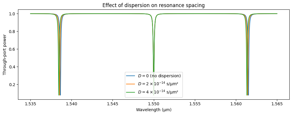
Dispersion breaks the strict periodicity of the resonance comb - the FSR varies gradually across the band.
Temperature Tuning
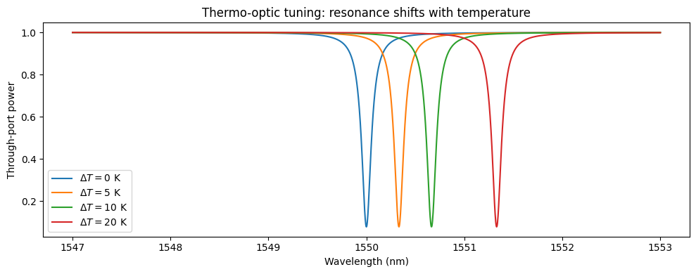
The dn_dT parameter captures the thermo-optic effect: how the effective index shifts with temperature. For silicon, \(\mathrm{d}n/\mathrm{d}T \approx 1.8 \times 10^{-4}\;\text{K}^{-1}\). A temperature change shifts all resonances by the same amount in frequency:
This is the operating principle of thermo-optic ring tuners used in WDM transceivers.
Tip:
temperatureandreference_temperaturecan be passed viamodel_kwargstos_matrixfor fast parameter sweeps without rebuilding the model.
[10]:
ring_thermo = pf.RingModel(
    kappa1=1j * 0.2,
    n_eff=n_eff_ring,
    n_group=n_group_ring,
    length=L_ring,
    propagation_loss=2e-3,
    dn_dT=1.8e-4,
    temperature=293.0,
    reference_temperature=293.0,
    reference_frequency=f0,
)
bb_thermo = ring_thermo.black_box_component(port_spec="Strip")

fig, ax = plt.subplots(figsize=(10, 4))

for dT in [0, 5, 10, 20]:
    s = bb_thermo.s_matrix(freqs_zoom, model_kwargs={"temperature": 293.0 + dT}, show_progress=False)
    ax.plot(wavelengths_zoom * 1e3, np.abs(s[thru_key]) ** 2, label=f"$\\Delta T = {dT}$ K")

ax.set_xlabel("Wavelength (nm)")
ax.set_ylabel("Through-port power")
ax.set_title("Thermo-optic tuning: resonance shifts with temperature")
ax.legend()
fig.tight_layout()
plt.show()
[11]:
# Verify the theoretical tuning rate
dn_dT_val = 1.8e-4      # K^-1
n_g = 4.2
lambda0 = 1.55e-6       # m

tuning_rate_nm_per_K = lambda0 / n_g * dn_dT_val * 1e9  # nm/K
print(f"Expected tuning rate: {tuning_rate_nm_per_K:.4f} nm/K")
Expected tuning rate: 0.0664 nm/K
Electro-Optic Ring Modulator
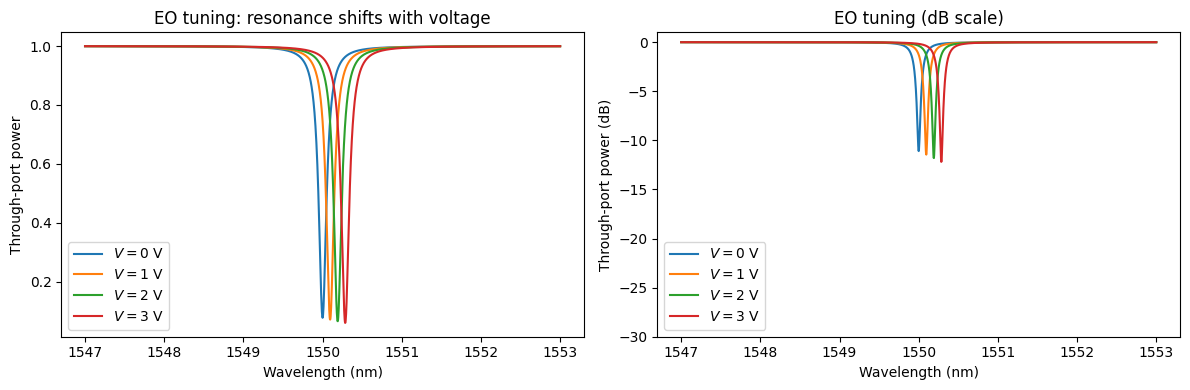
Silicon ring modulators work by electrically shifting the resonance via the plasma dispersion effect. The key parameters are:
dn_dv: Linear change in effective index per volt (1/V). A typical value for a silicon carrier-depletion microring is \(\mathrm{d}n/\mathrm{d}V \approx 2.6 \times 10^{-4}\) V\(^{-1}\), corresponding to \(V_\pi L \approx 3000\) V\(\cdot\mu\)m.dn_dv2: Quadratic correction. In practice \(V_\pi L\) varies with bias (see the section below), so ignoringdn_dv2overestimates the modulation efficiency on one side of the bias point and underestimates it on the other.dloss_dv: Linear voltage-dependent propagation loss (carrier absorption).
The voltage-length product convention used for MZMs (\(V_\pi L\)) maps to the ring as:
For \(V_\pi L = 3000\;\text{V}\cdot\mu\text{m}\) at 1550 nm: \(\mathrm{d}n/\mathrm{d}V \approx 1.55 / (2 \times 3000) \approx 2.58 \times 10^{-4}\) V\(^{-1}\), giving a resonance tuning rate of \(\approx 0.095\) nm/V.
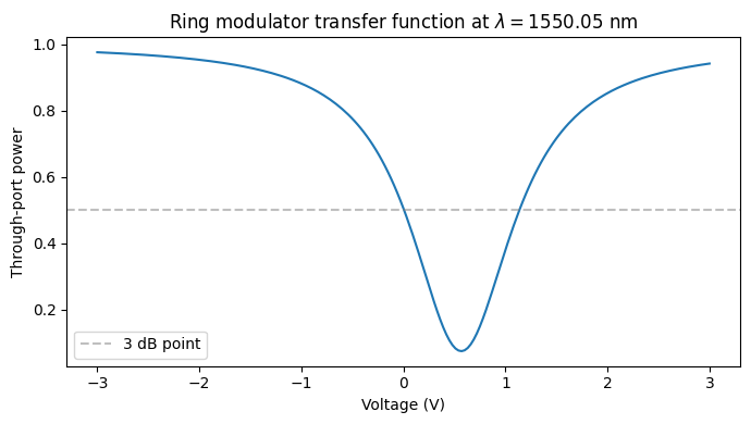
The ring modulator operates on the flank of the resonance: the laser is biased at the point of maximum slope (half-power point), so small voltage changes produce large intensity modulation.
[12]:
v_piL = 3000.0  # V*um  (typical high-performance Si carrier-depletion ring)
dn_dv_val = 1.55 / (2 * v_piL)   # 1/V, positive convention: +V red-shifts resonance

ring_mod = pf.RingModel(
    kappa1=1j * 0.2,
    n_eff=n_eff_ring,
    n_group=n_group_ring,
    length=L_ring,
    propagation_loss=2e-3,
    dn_dv=dn_dv_val,
    dloss_dv=5e-5,
    voltage=0.0,
    reference_frequency=f0,
)
bb_mod = ring_mod.black_box_component(port_spec="Strip")

print(f"dn/dV = {dn_dv_val:.4e} 1/V  (V_piL = {v_piL} V*um = {v_piL/1e4:.2f} V*cm)")
print(f"Resonance tuning rate = {1.55 * dn_dv_val / n_group_ring * 1e3:.4f} nm/V")

fig, axes = plt.subplots(1, 2, figsize=(12, 4))

for V in [0, 1, 2, 3]:
    s = bb_mod.s_matrix(freqs_zoom, model_kwargs={"voltage": V}, show_progress=False)
    T = np.abs(s[thru_key]) ** 2
    axes[0].plot(wavelengths_zoom * 1e3, T, label=f"$V = {V}$ V")
    axes[1].plot(wavelengths_zoom * 1e3, 10 * np.log10(T + 1e-30), label=f"$V = {V}$ V")

axes[0].set_xlabel("Wavelength (nm)")
axes[0].set_ylabel("Through-port power")
axes[0].set_title("EO tuning: resonance shifts with voltage")
axes[0].legend()

axes[1].set_xlabel("Wavelength (nm)")
axes[1].set_ylabel("Through-port power (dB)")
axes[1].set_ylim(-30, 1)
axes[1].set_title("EO tuning (dB scale)")
axes[1].legend()

fig.tight_layout()
plt.show()
dn/dV = 2.5833e-04 1/V  (V_piL = 3000.0 V*um = 0.30 V*cm)
Resonance tuning rate = 0.0953 nm/V
[13]:
# Transfer function at a fixed wavelength (biased at the resonance flank)
# First, find the wavelength of maximum slope near 1550 nm
s_v0 = bb_mod.s_matrix(freqs_zoom, model_kwargs={"voltage": 0}, show_progress=False)
T_v0 = np.abs(s_v0[thru_key]) ** 2

# Find half-power wavelength on the long-wavelength flank (blue side of resonance)
idx_res = np.argmin(T_v0)
idx_half = idx_res + np.argmin(np.abs(T_v0[idx_res:] - 0.5))
lambda_bias = wavelengths_zoom[idx_half]
f_bias = freqs_zoom[idx_half]
print(f"Bias wavelength (flank): {lambda_bias * 1e3:.3f} nm")

# Voltage sweep at the bias wavelength
voltages = np.linspace(-3, 3, 201)
T_vs_V = []
for V in voltages:
    s = bb_mod.s_matrix([f_bias], model_kwargs={"voltage": V}, show_progress=False)
    T_vs_V.append(np.abs(s[thru_key][0]) ** 2)
T_vs_V = np.array(T_vs_V)

fig, ax = plt.subplots(figsize=(7, 4))
ax.plot(voltages, T_vs_V)
ax.axhline(0.5, color="gray", linestyle="--", alpha=0.5, label="3 dB point")
ax.set_xlabel("Voltage (V)")
ax.set_ylabel("Through-port power")
ax.set_title(f"Ring modulator transfer function at $\\lambda = {lambda_bias*1e3:.2f}$ nm")
ax.legend()
fig.tight_layout()
plt.show()
Bias wavelength (flank): 1550.054 nm
Voltage-Dependent EO Modulation
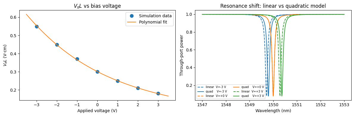
In practice the phase efficiency \(\mathrm{d}n/\mathrm{d}V\) is not constant with bias. For a silicon carrier-depletion junction, the depletion width widens under larger reverse bias, reducing the mode overlap with the junction capacitance and therefore increasing \(V_\pi L\). The dn_dv2 parameter captures this through a second-order Taylor expansion of the index change:
Starting from a simulated or measured \(V_\pi L(V)\) table, fit \(1/V_\pi L(V)\) to a first-order (linear) polynomial,
and read off the RingModel parameters directly:
dn_dv\(= \lambda_0\,c_0/2\)dn_dv2\(= \lambda_0\,c_1/4\)
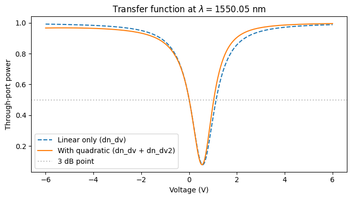
The quadratic term makes the transfer curve asymmetric: modulation efficiency is higher on the forward-bias side and lower on the deep reverse-bias side.
[14]:
# Representative VpiL(V) data for a silicon lateral p-n ring modulator.
# Negative voltage = reverse bias; VpiL increases with reverse bias as the
# depletion region grows and its overlap with the optical mode decreases.
voltages_data = np.array([-3.0, -2.0, -1.0, 0.0, 1.0, 2.0, 3.0])
vpiL_um_data  = np.array([5500., 4500., 3700., 3000., 2500., 2100., 1800.])  # V*um

# Fit 1/VpiL(V) to a first-order (linear) polynomial.
# np.polyfit returns [c1, c0] (highest degree first): p(V) = c1*V + c0
# A quadratic fit would produce a c2 term with no corresponding RingModel parameter.
inv_vpiL = 1.0 / vpiL_um_data
c1, c0 = np.polyfit(voltages_data, inv_vpiL, 1)

# RingModel parameters from polynomial coefficients (lam0 in um)
lam0 = 1.55
dn_dv_fit  = lam0 * c0 / 2   # 1/V
dn_dv2_fit = lam0 * c1 / 4   # 1/V^2

print(f"dn_dv  = {dn_dv_fit:.4e} 1/V   -> VpiL(0) = {lam0/(2*dn_dv_fit)/1e4:.2f} V*cm")
print(f"dn_dv2 = {dn_dv2_fit:.4e} 1/V^2")

# --- VpiL fit quality ---
voltages_plot = np.linspace(-3.5, 3.5, 200)
vpiL_fit = 1.0 / np.polyval([c1, c0], voltages_plot)

fig, axes = plt.subplots(1, 2, figsize=(12, 4))

axes[0].plot(voltages_data, vpiL_um_data / 1e4, "o", ms=8, label="Simulation data")
axes[0].plot(voltages_plot, vpiL_fit / 1e4, "-", label="Linear fit")
axes[0].set_xlabel("Applied voltage (V)")
axes[0].set_ylabel("$V_\\pi L$ (V$\\cdot$cm)")
axes[0].set_title("$V_\\pi L$ vs bias voltage")
axes[0].legend()

# --- Build models: linear-only vs full quadratic ---
ring_lin = pf.RingModel(
    kappa1=1j * 0.2,
    n_eff=n_eff_ring,
    n_group=n_group_ring,
    length=L_ring,
    propagation_loss=2e-3,
    dn_dv=dn_dv_fit,
    voltage=0.0,
    reference_frequency=f0,
)
ring_quad = pf.RingModel(
    kappa1=1j * 0.2,
    n_eff=n_eff_ring,
    n_group=n_group_ring,
    length=L_ring,
    propagation_loss=2e-3,
    dn_dv=dn_dv_fit,
    dn_dv2=dn_dv2_fit,
    voltage=0.0,
    reference_frequency=f0,
)
bb_lin  = ring_lin.black_box_component(port_spec="Strip")
bb_quad = ring_quad.black_box_component(port_spec="Strip")

for V, color in [(-3, "C0"), (0, "C1"), (3, "C2")]:
    s_l = bb_lin.s_matrix(freqs_zoom,  model_kwargs={"voltage": V}, show_progress=False)
    s_q = bb_quad.s_matrix(freqs_zoom, model_kwargs={"voltage": V}, show_progress=False)
    T_l = np.abs(s_l[thru_key])**2
    T_q = np.abs(s_q[thru_key])**2
    axes[1].plot(wavelengths_zoom * 1e3, T_l, ls="--", color=color, label=f"linear  V={V:+d} V")
    axes[1].plot(wavelengths_zoom * 1e3, T_q, ls="-",  color=color, label=f"quad    V={V:+d} V")

axes[1].set_xlabel("Wavelength (nm)")
axes[1].set_ylabel("Through-port power")
axes[1].set_title("Resonance shift: linear vs quadratic model")
axes[1].legend(fontsize=7, ncol=2)

fig.tight_layout()
plt.show()

# --- Transfer function at the resonance flank ---
s_v0 = bb_quad.s_matrix(freqs_zoom, model_kwargs={"voltage": 0}, show_progress=False)
T_v0 = np.abs(s_v0[thru_key])**2
idx_res  = np.argmin(T_v0)
idx_half = idx_res + np.argmin(np.abs(T_v0[idx_res:] - 0.5))
lambda_bias = wavelengths_zoom[idx_half]
f_bias = freqs_zoom[idx_half]
print(f"Bias wavelength (half-power flank): {lambda_bias * 1e3:.3f} nm")

voltages_sweep = np.linspace(-6, 6, 401)
T_lin_sweep  = [np.abs(bb_lin.s_matrix([f_bias],   model_kwargs={"voltage": V}, show_progress=False)[thru_key][0])**2
                for V in voltages_sweep]
T_quad_sweep = [np.abs(bb_quad.s_matrix([f_bias], model_kwargs={"voltage": V}, show_progress=False)[thru_key][0])**2
                for V in voltages_sweep]

fig, ax = plt.subplots(figsize=(7, 4))
ax.plot(voltages_sweep, T_lin_sweep,  "--", label="Linear only (dn_dv)")
ax.plot(voltages_sweep, T_quad_sweep, "-",  label="With quadratic (dn_dv + dn_dv2)")
ax.axhline(0.5, color="gray", ls=":", alpha=0.5, label="3 dB point")
ax.set_xlabel("Voltage (V)")
ax.set_ylabel("Through-port power")
ax.set_title(f"Transfer function at $\\lambda = {lambda_bias*1e3:.2f}$ nm")
ax.legend()
fig.tight_layout()
plt.show()
dn_dv  = 2.7008e-04 1/V   -> VpiL(0) = 0.29 V*cm
dn_dv2 = 2.4342e-05 1/V^2
Bias wavelength (half-power flank): 1550.054 nm
Add-Drop Ring (Double Bus)
Setting kappa2 adds a second bus waveguide to create a four-port add-drop filter. This is the standard topology for WDM wavelength routing:
Light at resonance couples from the input to the drop port.
Off-resonance light passes through to the through port.
The add port injects signals at the resonance into the through bus.
The second coupling coefficient kappa2 provides an independent control over the drop-port bandwidth. For a symmetric filter, set \(|\kappa_2| = |\kappa_1|\).
[15]:
ring_adddrop = pf.RingModel(
    kappa1=1j * 0.25,
    kappa2=1j * 0.25,   # second bus: symmetric add-drop
    n_eff=n_eff_ring,
    n_group=n_group_ring,
    length=L_ring,
    propagation_loss=2e-3,
    reference_frequency=f0,
)
bb_adddrop = ring_adddrop.black_box_component(port_spec="Strip")
bb_adddrop
[15]:

[16]:
pn_ad = sorted(bb_adddrop.s_matrix(freqs, show_progress=False).ports)
print("Ports:", pn_ad)

fig, axes = plt.subplots(1, 2, figsize=(12, 4))

for kappa_mag, ls, label in [
    (0.15, "-",  "Asymmetric ($|\\kappa_2| < |\\kappa_1|$)"),
    (0.25, "--", "Symmetric ($|\\kappa_2| = |\\kappa_1|$)"),
    (0.40, ":",  "Asymmetric ($|\\kappa_2| > |\\kappa_1|$)"),
]:
    m = pf.RingModel(
        kappa1=1j * 0.25,
        kappa2=1j * kappa_mag,
        n_eff=n_eff_ring,
        n_group=n_group_ring,
        length=L_ring,
        propagation_loss=2e-3,
        reference_frequency=f0,
    )
    bb = m.black_box_component(port_spec="Strip")
    s = bb.s_matrix(freqs_zoom, show_progress=False)
    tk = ("P0@0", "P1@0")
    dk = ("P0@0", "P2@0")
    wl_nm = wavelengths_zoom * 1e3
    axes[0].plot(wl_nm, 10 * np.log10(np.abs(s[tk]) ** 2 + 1e-30), ls=ls, label=label)
    axes[1].plot(wl_nm, 10 * np.log10(np.abs(s[dk]) ** 2 + 1e-30), ls=ls, label=label)

for ax, title in zip(axes, ["Through port", "Drop port"]):
    ax.set_xlabel("Wavelength (nm)")
    ax.set_ylabel("Power (dB)")
    ax.set_title(f"Add-drop ring: {title}")
    ax.set_ylim(-25, 1)
    ax.legend(fontsize=8)

fig.tight_layout()
plt.show()
Ports: ['P0', 'P1', 'P2', 'P3']
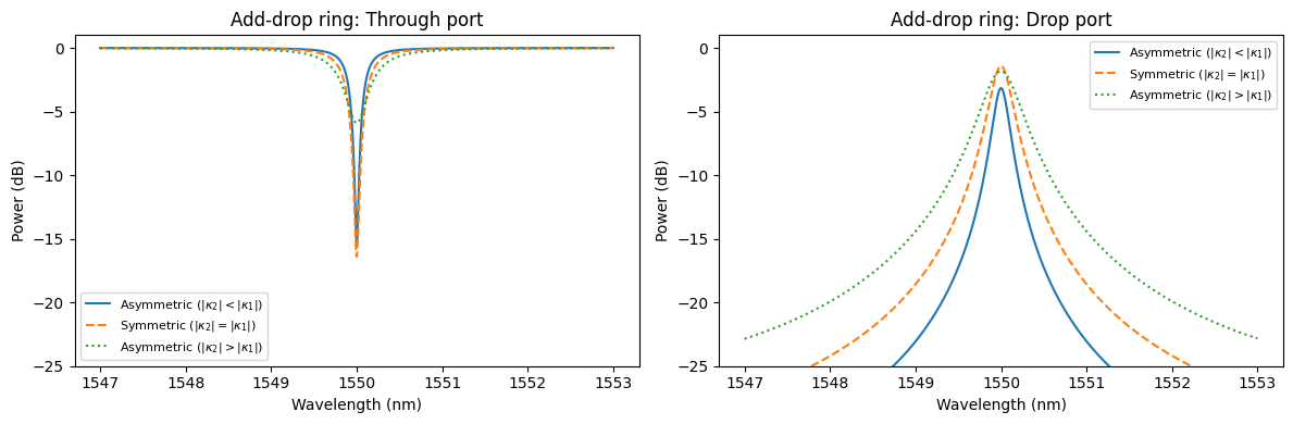
For the symmetric add-drop ring (\(|\kappa_1| = |\kappa_2|\)), the through port is not a perfect null at resonance - instead, exactly half the power (3 dB) arrives at the drop port when both coupling rates are equal. A larger \(|\kappa_2|\) broadens the drop-port bandwidth and shifts the coupling regime.
Parameter Reference
The table below summarizes all RingModel parameters and their physical meaning:
Parameter |
Units |
Physical meaning |
|---|---|---|
|
Field coupling coefficient, first bus. \(|\kappa_1|^2\) = power coupled in/out per round-trip. Phase sets the coupler convention. |
|
|
Field coupling coefficient, second bus ( |
|
|
Effective refractive index. Sets the resonance wavelength positions. |
|
|
Group index. Sets the FSR ≈ \(\lambda^2/(n_g L)\). Defaults to |
|
|
µm |
Ring round-trip circumference. Longer ring → smaller FSR. |
|
dB/µm |
Round-trip waveguide loss. Controls the intrinsic Q and the critical coupling condition. |
|
s/µm² |
Chromatic dispersion \(D\). Makes FSR wavelength-dependent. |
|
s/µm³ |
Higher-order dispersion. |
|
Hz |
Center frequency for the Taylor expansion of \(\beta(f)\). |
|
1/K |
Thermo-optic coefficient. Shifts resonances with temperature. |
|
dB/µm/K |
Temperature-dependent loss coefficient. |
|
K |
Operating temperature. |
|
K |
Temperature at which |
|
V |
Applied voltage for EO modulation. |
|
1/V |
Linear EO index change. Equivalent to \(\lambda/(2 V_\pi L)\). |
|
1/V² |
Quadratic EO index change. |
|
dB/µm/V |
Linear voltage-dependent loss (carrier absorption). |
|
dB/µm/V² |
Quadratic voltage-dependent loss. |