
Technology and PDK Setup
This notebook builds a custom SiEPIC EBeam technology stack (PDK “technology”) intended for high-speed RF photonics work (modulators, transceivers), then validates/visualizes it by:
printing a technology summary (layers / extrusion specs / ports),
plotting a representative cross-section,
listing the available PDK components,
instantiating one example component.
Conventions
Geometry dimensions are in µm.
Frequencies are in Hz.
The PDK/technology in this project is implemented so that PIC designers can:
Understand the process stack quickly (layer thicknesses, materials, and key assumptions).
Modify the stack (e.g., oxide thickness, metal thickness/conductivity) without rewriting the whole PDK.
Translate the technology definition to other toolchains and formats.
In this notebook, the customization points are intentionally kept in a small set of named parameters (waveguide geometry, oxide stack, and metal stack), so you can reuse the same pattern for other foundry stacks.

Figure: The technology wrapper exposes a small set of parameters (materials + layer thicknesses) that define the process stack used in layout, visualization, and simulation.
Technology Stack Configuration
In the next cells we define the process stack parameters (waveguide geometry, oxide thicknesses, and metal stack) and the material models used by PhotonForge/Tidy3D.
The goal is to keep all tunable knobs centralized and clearly named so the stack can be reused across projects (or mapped to a foundry PDK).
This section sets up the SiEPIC EBeam technology with a few customizations aimed at high-speed RF photonics applications (modulators, transceivers).
Parameter |
Default PDK |
This Config |
|---|---|---|
top_oxide_thickness |
0.3 µm |
1.5 µm |
bottom_oxide_thickness |
3.017 µm |
2.0 µm |
metal_si_separation |
2.2 µm |
1.28 µm |
router_thickness |
0.6 µm |
2.0 µm |
router_metal |
Au (σ=17) |
Al (σ=38) |
heater_metal |
W (σ=1.6) |
Doped Si (σ=0.2) |
include_top_opening |
False |
True |
include_substrate |
False |
True |
Key customizations vs SiEPIC EBeam defaults
Thicker metal (2 µm Al) for better RF performance and lower loss.
Oxide thicknesses chosen to match a realistic process stack.
Higher conductivity Al for transmission-line electrodes.
Cross-section visualization includes air and substrate so the full stack is visible. This is aligned with the real chip stack where air and substrate are present.
[1]:
# Imports used throughout this notebook:
import tidy3d as td
import photonforge as pf
import numpy as np
import siepic_forge as siepic
from matplotlib import pyplot as plt
07:24:48 -03 WARNING: The material-library variant 'Palik_Lossless' is
             deprecated and maps to 'Palik_LowLoss' because it contains a tiny
             fitted loss despite its name. Use 'Palik_NoLoss' where available
             for a zero-loss Palik model.
[2]:
# Process / geometry parameters (units: µm)

# Waveguide geometry (kept consistent with the default EBeam PDK)
H_CORE = 0.22       # Silicon device/core thickness (µm)
H_SLAB = 0.09       # Silicon slab thickness for rib waveguides (µm)
W_CORE = 0.5        # Nominal waveguide width (µm)

# Oxide thicknesses
TOX_THICKNESS = 1.5  # Top oxide cladding thickness (µm)
BOX_THICKNESS = 2.0  # Buried oxide (BOX) thickness (µm)

# Metal stack (RF routing / heaters)
TL_THICKNESS = 2.0   # Router/heater metal thickness (µm)
[3]:
# Define aluminum for both optical and electrical simulations.
# We use Tidy3D's optical material model plus a (frequency-dependent) electrical medium.
al_metal = {
    "optical": td.material_library["Al"]["Rakic1995"],
    "electrical": td.LossyMetalMedium(
        conductivity=38,  # Conductivity in S/µm (≈ 38e6 S/m)
        frequency_range=[0.1e9, 200e9],  # Hz
        fit_param=td.SurfaceImpedanceFitterParam(max_num_poles=16),
    ),
}

# Doped silicon heater layer:
# Optical properties are approximated using pure Si, assuming negligible optical interaction.
doped_si = {
    "optical": td.material_library["cSi"]["Li1993_293K"],
    "electrical": td.LossyMetalMedium(
        conductivity=0.2,  # Conductivity in S/µm (≈ 2e5 S/m)
        frequency_range=[0.1e9, 200e9],  # Hz
        fit_param=td.SurfaceImpedanceFitterParam(max_num_poles=16),
    ),
}
Create Custom Technology
Here we instantiate a Technology object by calling siepic.ebeam(...) and overriding the key stack parameters defined above.
The returned
techobject is used by PhotonForge for layout and for Tidy3D-based visualization/simulation.We also set
pf.config.default_technologyso subsequent components use this stack by default.
[4]:
# Build the Technology object with our custom stack parameters.
# This object controls layer definitions, vertical extrusions (cross-sections), and port definitions.
tech = siepic.ebeam(
    # Si layer
    si_thickness=H_CORE,
    si_slab_thickness=H_SLAB,

    # Oxide stack
    top_oxide_thickness=TOX_THICKNESS,
    bottom_oxide_thickness=BOX_THICKNESS,

    # Metal stack
    router_thickness=TL_THICKNESS,
    router_metal=al_metal,
    heater_metal=doped_si,
)

# Revise the "TE_1550_500" port in accordance with W_CORE
tech.ports["TE_1550_500"].path_profiles = [(W_CORE, 0.0, (1, 0))]

# Set this technology as the default for the project
pf.config.default_technology = tech
[5]:
# Display a summary table of layers/ports/extrusions (sanity check)
tech
[5]:
Layers
| Name | Layer | Description | Color | Pattern |
|---|---|---|---|---|
| Si | (1, 0) | SiEPIC - Waveguide | #ff80a818 | \\ |
| PinRec | (1, 10) | SiEPIC | #ff80a818 | xx |
| PinRecM | (1, 11) | SiEPIC | #80000018 | + |
| Si Slab | (2, 0) | Dedicated Run Layers - Device…… Layer Partial Etch | #c080ff18 | / |
| Direct Metal | (5, 0) | Dedicated Run Layers | #80a8ff18 | || |
| Oxide open to BOX | (6, 0) | Dedicated Run Layers | #ff000018 | - |
| Text | (10, 0) | Text-Not Fabricated | #00000018 | hollow |
| M1_heater | (11, 0) | TiW Heater | #0000ff18 | \\ |
| M2_router | (12, 0) | TiW/Au Routing Bilayer | #ffbf0018 | // |
| M_Open | (13, 0) | Bond Pad Open | #80005718 | \\ |
| Si n | (20, 0) | Dedicated Run Layers | #afff8018 | - |
| Si p | (21, 0) | Dedicated Run Layers | #ffd9df18 | = |
| Si n+ | (22, 0) | Dedicated Run Layers | #ff800018 | x |
| Si p+ | (23, 0) | Dedicated Run Layers | #ddff0018 | xx |
| Si n++ | (24, 0) | Dedicated Run Layers | #00ffff18 | + |
| Si p++ | (25, 0) | Dedicated Run Layers | #00800018 | ++ |
| ANT Reserved | (31, 0) | SiEPIC/ANT Reserved | #9580ff18 | / |
| ANT Reserved 1 | (33, 0) | ANT Reserved | #9580ff18 | / |
| Via to silicon | (40, 0) | Dedicated Run Layers | #0000ff18 | . |
| DevRec | (68, 0) | SiEPIC | #00800018 | . |
| FbrTgt | (81, 0) | SiEPIC/Dedicated Run Layers | #80808018 | ++ |
| ANT Reserved 2 | (102, 0) | ANT Reserved | #9580ff18 | / |
| ANT Reserved 3 | (110, 0) | ANT Reserved | #9580ff18 | / |
| Custom Dicing | (189, 0) | #00000018 | hollow | |
| SEM Imaging | (200, 0) | #ff000018 | x | |
| Deep Trench | (201, 0) | #00ff0018 | . | |
| Deep Trench Handling Exclusion | (202, 0) | #00760018 | : | |
| Thermal Isolation Trenches | (203, 0) | #00800018 | \ | |
| Laser Integration Shelf | (205, 0) | Dedicated Run Layers | #69ff0518 | xx |
| Floor Plan-Not Fabricated | (290, 0) | #c080ff18 | hollow | |
Error: device layer width is…… less than design rule | (301, 0) | DRC Errors | #80005718 | = |
Error: device layer spacing is…… less than design rule | (301, 1) | DRC Errors | #80005718 | - |
Warning: polygons/paths on…… PinRec layer (1/10) will NOT be fabricated | (301, 2) | DRC Errors | #80005718 | || |
Error: direct metal width is…… less than 5 microns | (305, 0) | DRC Errors | #80808018 | ++ |
Error: direct metal spacing is…… less than 10 microns | (305, 1) | DRC Errors | #80808018 | + |
Error: TiW width is less than 3…… microns | (311, 0) | DRC Errors | #ffa08018 | // |
Error: TiW spacing is less than…… 3 microns | (311, 1) | DRC Errors | #ffa08018 | / |
Error: Al width is less than…… design rule | (312, 0) | DRC Errors | #00ffff18 | | |
Error: Al spacing is less than…… design rule | (312, 1) | DRC Errors | #00ffff18 | // |
Error: Spacing between TiW and…… Al is less than 5 microns | (312, 3) | DRC Errors | #00ffff18 | \\ |
Error: Oxide window width is…… less than 10 microns | (313, 0) | DRC Errors | #01ff6b18 | || |
Error: Oxide window spacing is…… less than 10 microns | (313, 1) | DRC Errors | #01ff6b18 | | |
Error: Oxide window is not…… placed over Al | (313, 2) | DRC Errors | #01ff6b18 | // |
| Standard Design Area | (350, 0) | DRC Errors | #ddff0018 | \ |
Error: Features outside design…… area. Verify design size and centering. | (350, 1) | DRC Errors | #ddff0018 | : |
Error: Dicing lane width is…… less than 100 microns | (389, 0) | DRC Errors | #ff00ff18 | ++ |
Error: Spacing between dicing…… lane and devices is less than 50 microns | (389, 1) | DRC Errors | #ff00ff18 | + |
Error: SEM width is less than…… 500 nm | (400, 0) | DRC Errors | #ff9d9d18 | x |
| Deep Trench Design Area | (401, 0) | DRC Errors | #80a8ff18 | xx |
Error: Metal, SEM, or handling…… region overlap with deep trenches. Verify design centering | (401, 1) | DRC Errors | #80a8ff18 | x |
Warning: Silicon features…… outside deep trench design area. Verify accuracy before submission | (401, 2) | DRC Errors | #80a8ff18 | = |
Error: Spacing between metal…… and deep trench is less than 30 microns | (401, 3) | DRC Errors | #80a8ff18 | - |
Error: Deep trench width is…… less than 260 microns | (401, 4) | DRC Errors | #80a8ff18 | || |
Error: Deep trench handling…… area missing. Please add handling area of size shown by polygons | (402, 0) | DRC Errors | #ff000018 | + |
Error: Features inside deep…… trench handling area | (402, 1) | DRC Errors | #ff000018 | xx |
Error: Thermal isolation width…… is less than design rule | (403, 0) | DRC Errors | #50008018 | ++ |
Error: Thermal isolation…… spacing is less than design rule | (403, 1) | DRC Errors | #50008018 | + |
Error: Spacing between thermal…… isolation and metal is less than design rule | (403, 2) | DRC Errors | #50008018 | xx |
Error: Thermal isolation and…… device layer overlap, or spacing is less than design rule | (403, 3) | DRC Errors | #50008018 | x |
Dream Photonics Black Box-Not…… Fabricated | (998, 0) | #00000018 | hollow | |
| Errors | (999, 0) | SiEPIC | #0000ff18 | || |
Extrusion Specs
| # | Mask | Limits (μm) | Sidewal (°) | Opt. Medium | Elec. Medium |
|---|---|---|---|---|---|
| 0 | () | -inf, 0 | 0 | cSi_Li1993_293K | Si |
| 1 | () | -2, 1.8 | 0 | SiO2_Palik_LowLoss | SiO2 |
| 2 | 'M1_heater'**0.3 | 1.5, 2 | 0 | SiO2_Palik_LowLoss | SiO2 |
| 3 | 'M2_router'**0.3 | 1.5, 4 | 0 | SiO2_Palik_LowLoss | SiO2 |
| 4 | 'M1_heater' | 1.5, 1.7 | 0 | cSi_Li1993_293K | LossyMetalMedium……(frequency_range=(100000000.0, 200000000000.0), conductivity=0.2, fit_param={'max_num_poles': 16}) |
| 5 | 'M2_router' | 1.7, 3.7 | 0 | Al_Rakic1995 | LossyMetalMedium……(frequency_range=(100000000.0, 200000000000.0), conductivity=38.0, fit_param={'max_num_poles': 16}) |
| 6 | 'M_Open' | 3.7, 4 | 0 | Medium() | Medium() |
| 7 | 'Oxide open to BOX' | 0, inf | 0 | Medium() | Medium() |
| 8 | 'Si' | 0, 0.22 | 0 | cSi_Li1993_293K | Si |
| 9 | 'Si Slab' | 0, 0.09 | 0 | cSi_Li1993_293K | Si |
| 10 | 'Deep Trench' +…… 'Thermal Isolation Trenches' | -inf, inf | 0 | Medium() | Medium() |
Ports
| Name | Classification | Description | Width (μm) | Limits (μm) | Radius (μm) | Modes | Target n_eff | Path profiles (μm) | Voltage path | Current path |
|---|---|---|---|---|---|---|---|---|---|---|
| MM_TE_1550_2000 | optical | Multimode Strip TE 1550 nm,…… w=2000 nm | 6 | -2, 2.22 | 0 | 10 | 3.5 | 'Si': 2 | ||
| MM_TE_1550_3000 | optical | Multimode Strip TE 1550 nm,…… w=3000 nm | 6 | -2, 2.22 | 0 | 15 | 3.5 | 'Si': 3 | ||
| Rib_TE_1310_350 | optical | Rib (90 nm slab) TE 1310 nm,…… w=350 nm | 2.35 | -0.6, 0.82 | 0 | 1 | 3.5 | 'Si': 0.35, 'Si…… Slab': 3 | ||
| Rib_TE_1550_500 | optical | Rib (90 nm slab) TE 1550 nm,…… w=500 nm | 2.5 | -0.6, 0.82 | 0 | 1 | 3.5 | 'Si': 0.5, 'Si…… Slab': 3 | ||
| Slot_TE_1550_500 | optical | Slot TE 1550 nm, w=500 nm,…… gap=100nm | 3 | -1, 1.22 | 0 | 1 | 3.5 | 'Si': 0.2 (-0.15),…… 'Si': 0.2 (+0.15) | ||
| TE-TM_1550_450 | optical | Strip TE-TM 1550, w=450 nm | 2.2 | -1, 1.22 | 0 | 2 | 3.5 | 'Si': 0.45 | ||
| TE_1310_350 | optical | Strip TE 1310 nm, w=350 nm | 1.5 | -0.6, 0.82 | 0 | 1 | 3.5 | 'Si': 0.35 | ||
| TE_1310_410 | optical | Strip TE 1310 nm, w=410 nm | 1.5 | -0.6, 0.82 | 0 | 1 | 3.5 | 'Si': 0.41 | ||
| TE_1550_500 | optical | Strip TE 1550 nm, w=500 nm | 1.5 | -0.6, 0.82 | 0 | 1 | 3.5 | 'Si': 0.5 | ||
| TM_1310_350 | optical | Strip TM 1310 nm, w=350 nm | 1.5 | -0.6, 0.82 | 0 | 1 + 1 (TM) | 3.5 | 'Si': 0.35 | ||
| TM_1550_500 | optical | Strip TM 1550 nm, w=500 nm | 1.5 | -0.6, 0.82 | 0 | 1 + 1 (TM) | 3.5 | 'Si': 0.5 | ||
| eskid_TE_1550 | optical | eskid TE 1550 | 2 | -0.7, 0.92 | 0 | 1 | 3.5 | 'Si': 0.35,…… 'Si': 0.06 (+0.265), 'Si': 0.06 (-0.265), 'Si': 0.06 (+0.385), 'Si': 0.06 (-0.385), 'Si': 0.06 (+0.505), 'Si': 0.06 (-0.505), 'Si': 0.06 (+0.625), 'Si': 0.06 (-0.625) |
Background medium
- Optical: Medium()
- Electrical: Medium()
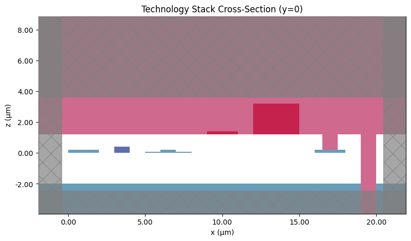
Plot technology cross-section
Before using the PDK in a larger design, it’s good practice to sanity-check the stack visually.
The helper function below:
builds a small “test” component containing shapes on representative layers (Si, SiN, metals, oxide opening, trench),
plots a cross-section at y = 0 using
pf.tidy3d_plot.
In the plot, x is the lateral position and z is the vertical stack height (both in µm).
[6]:
def plot_technology_cross_section(tech):
    """
    Create a test component and plot its cross-section to visualize
    the technology stack.

    Args:
        tech: PhotonForge Technology object
    """
    # Create test component with various layer types
    c = pf.Component("Technology_Cross_Section", technology=tech)

    # Add test structures on different layers
    c.add(
        # Silicon waveguide (full etch)
        "Si", pf.Rectangle((0, -0.5), (2, 0.5)),

        # Rib waveguide (slab + core)
        "Si Slab", pf.Rectangle((5, -1.5), (8, 1.5)),
        "Si", pf.Rectangle((6, -0.25), (7, 0.25)),

        # Heater metal
        "M1_heater", pf.Rectangle((9, -0.5), (11, 0.5)),

        # Router metal with via opening
        "M2_router", pf.Rectangle((12, -1), (15, 1)),
        "M_Open", pf.Rectangle((13, -0.5), (14, 0.5)),

        # Oxide opening (to BOX)
        "Si", pf.Rectangle((16, -0.5), (18, 0.5)),
        "Oxide open to BOX", pf.Rectangle((16.5, -0.3), (17.5, 0.3)),

        # Deep trench
        "Deep Trench", pf.Rectangle((19, -0.5), (20, 0.5)),
    )

    # Plot cross-section at y=0
    fig, ax = plt.subplots(figsize=(14, 5))
    pf.tidy3d_plot(c, y=0, ax=ax)
    ax.set_title("Technology Stack Cross-Section (y=0)")
    ax.set_xlabel("x (μm)")
    ax.set_ylabel("z (μm)")

    return c
[7]:
# Generate and display a simple cross-section sanity-check plot
plot_technology_cross_section(tech)
[7]:

List of available components in the PDK
siepic_forge exposes the set of available components via siepic.component_names.
Use this list to discover valid names to instantiate with siepic.component(name).
[8]:
# All component names exposed by this PDK wrapper
siepic.component_names
[8]:
{'GC_TE_1310_8degOxide_BB',
 'GC_TE_1550_8degOxide_BB',
 'GC_TM_1310_8degOxide_BB',
 'GC_TM_1550_8degOxide_BB',
 'ebeam_adiabatic_te1550',
 'ebeam_adiabatic_tm1550',
 'ebeam_bdc_te1550',
 'ebeam_crossing4',
 'ebeam_gc_te1550',
 'ebeam_gc_tm1550',
 'ebeam_routing_taper_te1550_w=500nm_to_w=3000nm_L=20um',
 'ebeam_routing_taper_te1550_w=500nm_to_w=3000nm_L=40um',
 'ebeam_splitter_swg_assist_te1310',
 'ebeam_splitter_swg_assist_te1550',
 'ebeam_terminator_te1310',
 'ebeam_terminator_te1550',
 'ebeam_terminator_tm1550',
 'ebeam_y_1310',
 'ebeam_y_1550',
 'ebeam_y_adiabatic',
 'ebeam_y_adiabatic_500pin',
 'taper_si_simm_1310',
 'taper_si_simm_1550'}
Load an example PDK component
Below we instantiate one component from the library and render it.
This is a quick check that the PDK is installed correctly and that the component’s layers/ports are available.
Tip: replace the component name with any entry from siepic.component_names.
[9]:
# Instantiate one component by name (change this string to explore the library)
siepic.component("ebeam_y_adiabatic_500pin")
[9]:
