
3D doping extrusion from a 2D carrier profile
Importing realistic doping profiles for charge transport and electro-optic simulations is typically a non-trivial task, as the doping geometries defined in physical layouts can be highly complex. In this notebook, we demonstrate how PhotonForge simplifies the process of loading and mapping 2D doping profiles directly onto these complex 3D layout geometries.

This notebook demonstrates an end-to-end workflow to:
Define optical + electrical materials for Si / SiO2 / metal contacts
Extend a foundry technology with custom mask layers for doped regions and contacts
Build a simple waveguide component
Create a 2D carrier density profile
Extrude that 2D profile along a curved waveguide to form a full 3D donor/acceptor distribution
Attach the resulting 3D doping to Tidy3D structures for downstream charge and/or FDTD simulations
PhotonForge’s technology maps 2D layout masks → 3D extruded structures. We use that same mapping for geometry (where doped regions exist), and then attach physics data (spatially varying donor/acceptor densities) to the resulting semiconductor medium.
Data flow (what gets built):
Layout masks: waveguide + slab + doping masks + contact masks.
Extrusion specs: define which masks become which 3D materials (and their z-spans).
2D carrier profile: arrays
n_a(x,z)andn_d(x,z)(in cm⁻³).3D voxelization: build
n_a(x,y,z)andn_d(x,y,z)on a global grid.Medium update: wrap the 3D arrays in SpatialDataArray and inject them into a MultiPhysicsMedium.
Structure update: replace the placeholder “Doped Si” medium in the generated structure list.
Notes
The numeric values and profile functions are illustrative; replace them with your process data as needed.
This notebook focuses on how to wire the data into the technology + simulation objects.
Technology setup
We import PhotonForge, a reference technology, and Tidy3D. We also lower Tidy3D logging verbosity so the notebook output stays focused on the workflow.
[1]:
import matplotlib.pyplot as plt
import numpy as np
import photonforge as pf
import siepic_forge as siepic
import tidy3d as td
td.config.logging.level = "ERROR"
07:27:51 -03 WARNING: The material-library variant 'Palik_Lossless' is
             deprecated and maps to 'Palik_LowLoss' because it contains a tiny
             fitted loss despite its name. Use 'Palik_NoLoss' where available
             for a zero-loss Palik model.
Define multiphysics materials (Si / SiO2 / contact)
We define:
silicon as a multiphysics semiconductor (optical permittivity + charge transport),
oxide as an insulator,
and a metal/contact medium for electrical terminals.
These material definitions will be referenced by the technology extrusion specs.
[2]:
charge_spec = td.SemiconductorMedium(
    permittivity=11.7,
    N_c=2.86e19,
    N_v=3.1e19,
    E_g=1.11,
    mobility_n=td.CaugheyThomasMobility(
        mu_min=52.2,
        mu=1471.0,
        ref_N=9.68e16,
        exp_N=0.68,
        exp_1=-0.57,
        exp_2=-2.33,
        exp_3=2.4,
        exp_4=-0.146,
    ),
    mobility_p=td.CaugheyThomasMobility(
        mu_min=44.9,
        mu=470.5,
        ref_N=2.23e17,
        exp_N=0.719,
        exp_1=-0.57,
        exp_2=-2.33,
        exp_3=2.4,
        exp_4=-0.146,
    ),
)

# Package optical and electrical definitions together for convenience.
si = {
    "optical": td.material_library["cSi"]["Li1993_293K"],
    "electrical": td.MultiPhysicsMedium(
        optical=td.Medium(permittivity=11.7),
        charge=charge_spec,
        name="Si",
    ),
}

# Metal contact: optical metal (Au) + an electrical conductor model.
contact_medium = {
    "optical": td.material_library["Au"]["JohnsonChristy1972"],
    "electrical": td.MultiPhysicsMedium(
        optical=td.PECMedium(
            viz_spec=td.VisualizationSpec(facecolor="#c2c4c3", alpha=1)
        ),
        charge=td.ChargeConductorMedium(conductivity=1),
        name="Contact",
    ),
}

# Oxide: electrical insulator + optical dielectric.
sio2 = {
    "optical": td.material_library["SiO2"]["Palik_Lossless"],
    "electrical": td.MultiPhysicsMedium(
        optical=td.Medium(permittivity=3.9),
        charge=td.ChargeInsulatorMedium(permittivity=3.9),
        name="SiO2",
    ),
}
Create a working technology instance
We start from a reference foundry technology (SiEPIC EBeam) and override its base media with the optical/electrical definitions from above. Then we set it as the default technology for subsequent PhotonForge components.
[3]:
tech = siepic.ebeam(si=si, sio2=sio2)

pf.config.default_technology = tech
pf.config.svg_labels = False
Then we add custom GDS mask layers for P / P++ and Contact. These layers are later used to decide where the 3D “Doped Si” and contact extrusions should exist.
[4]:
p_layer = pf.LayerSpec(
    layer=(21, 0), description="P Doping", color="#03fcd718", pattern="\\"
)

pp_layer = pf.LayerSpec(
    layer=(25, 0), description="P++ Doping", color="#0c7d5d18", pattern="\\"
)

contact_layer = pf.LayerSpec(
    layer=(14, 0), description="Metal_contact", color="#c2c4c318", pattern="solid"
)

tech.add_layer("Si P", p_layer)
tech.add_layer("Si P++", pp_layer)
tech.add_layer("Contact", contact_layer)
[4]:
Layers
| Name | Layer | Description | Color | Pattern |
|---|---|---|---|---|
| Si | (1, 0) | SiEPIC - Waveguide | #ff80a818 | \\ |
| PinRec | (1, 10) | SiEPIC | #ff80a818 | xx |
| PinRecM | (1, 11) | SiEPIC | #80000018 | + |
| Si Slab | (2, 0) | Dedicated Run Layers - Device…… Layer Partial Etch | #c080ff18 | / |
| Direct Metal | (5, 0) | Dedicated Run Layers | #80a8ff18 | || |
| Oxide open to BOX | (6, 0) | Dedicated Run Layers | #ff000018 | - |
| Text | (10, 0) | Text-Not Fabricated | #00000018 | hollow |
| M1_heater | (11, 0) | TiW Heater | #0000ff18 | \\ |
| M2_router | (12, 0) | TiW/Au Routing Bilayer | #ffbf0018 | // |
| M_Open | (13, 0) | Bond Pad Open | #80005718 | \\ |
| Contact | (14, 0) | Metal_contact | #c2c4c318 | solid |
| Si n | (20, 0) | Dedicated Run Layers | #afff8018 | - |
| Si P | (21, 0) | P Doping | #03fcd718 | \ |
| Si p | (21, 0) | Dedicated Run Layers | #ffd9df18 | = |
| Si n+ | (22, 0) | Dedicated Run Layers | #ff800018 | x |
| Si p+ | (23, 0) | Dedicated Run Layers | #ddff0018 | xx |
| Si n++ | (24, 0) | Dedicated Run Layers | #00ffff18 | + |
| Si P++ | (25, 0) | P++ Doping | #0c7d5d18 | \ |
| Si p++ | (25, 0) | Dedicated Run Layers | #00800018 | ++ |
| ANT Reserved | (31, 0) | SiEPIC/ANT Reserved | #9580ff18 | / |
| ANT Reserved 1 | (33, 0) | ANT Reserved | #9580ff18 | / |
| Via to silicon | (40, 0) | Dedicated Run Layers | #0000ff18 | . |
| DevRec | (68, 0) | SiEPIC | #00800018 | . |
| FbrTgt | (81, 0) | SiEPIC/Dedicated Run Layers | #80808018 | ++ |
| ANT Reserved 2 | (102, 0) | ANT Reserved | #9580ff18 | / |
| ANT Reserved 3 | (110, 0) | ANT Reserved | #9580ff18 | / |
| Custom Dicing | (189, 0) | #00000018 | hollow | |
| SEM Imaging | (200, 0) | #ff000018 | x | |
| Deep Trench | (201, 0) | #00ff0018 | . | |
| Deep Trench Handling Exclusion | (202, 0) | #00760018 | : | |
| Thermal Isolation Trenches | (203, 0) | #00800018 | \ | |
| Laser Integration Shelf | (205, 0) | Dedicated Run Layers | #69ff0518 | xx |
| Floor Plan-Not Fabricated | (290, 0) | #c080ff18 | hollow | |
Error: device layer width is…… less than design rule | (301, 0) | DRC Errors | #80005718 | = |
Error: device layer spacing is…… less than design rule | (301, 1) | DRC Errors | #80005718 | - |
Warning: polygons/paths on…… PinRec layer (1/10) will NOT be fabricated | (301, 2) | DRC Errors | #80005718 | || |
Error: direct metal width is…… less than 5 microns | (305, 0) | DRC Errors | #80808018 | ++ |
Error: direct metal spacing is…… less than 10 microns | (305, 1) | DRC Errors | #80808018 | + |
Error: TiW width is less than 3…… microns | (311, 0) | DRC Errors | #ffa08018 | // |
Error: TiW spacing is less than…… 3 microns | (311, 1) | DRC Errors | #ffa08018 | / |
Error: Al width is less than…… design rule | (312, 0) | DRC Errors | #00ffff18 | | |
Error: Al spacing is less than…… design rule | (312, 1) | DRC Errors | #00ffff18 | // |
Error: Spacing between TiW and…… Al is less than 5 microns | (312, 3) | DRC Errors | #00ffff18 | \\ |
Error: Oxide window width is…… less than 10 microns | (313, 0) | DRC Errors | #01ff6b18 | || |
Error: Oxide window spacing is…… less than 10 microns | (313, 1) | DRC Errors | #01ff6b18 | | |
Error: Oxide window is not…… placed over Al | (313, 2) | DRC Errors | #01ff6b18 | // |
| Standard Design Area | (350, 0) | DRC Errors | #ddff0018 | \ |
Error: Features outside design…… area. Verify design size and centering. | (350, 1) | DRC Errors | #ddff0018 | : |
Error: Dicing lane width is…… less than 100 microns | (389, 0) | DRC Errors | #ff00ff18 | ++ |
Error: Spacing between dicing…… lane and devices is less than 50 microns | (389, 1) | DRC Errors | #ff00ff18 | + |
Error: SEM width is less than…… 500 nm | (400, 0) | DRC Errors | #ff9d9d18 | x |
| Deep Trench Design Area | (401, 0) | DRC Errors | #80a8ff18 | xx |
Error: Metal, SEM, or handling…… region overlap with deep trenches. Verify design centering | (401, 1) | DRC Errors | #80a8ff18 | x |
Warning: Silicon features…… outside deep trench design area. Verify accuracy before submission | (401, 2) | DRC Errors | #80a8ff18 | = |
Error: Spacing between metal…… and deep trench is less than 30 microns | (401, 3) | DRC Errors | #80a8ff18 | - |
Error: Deep trench width is…… less than 260 microns | (401, 4) | DRC Errors | #80a8ff18 | || |
Error: Deep trench handling…… area missing. Please add handling area of size shown by polygons | (402, 0) | DRC Errors | #ff000018 | + |
Error: Features inside deep…… trench handling area | (402, 1) | DRC Errors | #ff000018 | xx |
Error: Thermal isolation width…… is less than design rule | (403, 0) | DRC Errors | #50008018 | ++ |
Error: Thermal isolation…… spacing is less than design rule | (403, 1) | DRC Errors | #50008018 | + |
Error: Spacing between thermal…… isolation and metal is less than design rule | (403, 2) | DRC Errors | #50008018 | xx |
Error: Thermal isolation and…… device layer overlap, or spacing is less than design rule | (403, 3) | DRC Errors | #50008018 | x |
Dream Photonics Black Box-Not…… Fabricated | (998, 0) | #00000018 | hollow | |
| Errors | (999, 0) | SiEPIC | #0000ff18 | || |
Extrusion Specs
| # | Mask | Limits (μm) | Sidewal (°) | Opt. Medium | Elec. Medium |
|---|---|---|---|---|---|
| 0 | () | -inf, 0 | 0 | cSi_Li1993_293K | MultiPhysicsMedium(name=……'Si', optical={'permittivity': 11.7}, charge={'permittivity': 11.7, 'N_c': {'N': 2.86e+19}, 'N_v': {'N': 3.1e+19}, 'E_g': {'eg': 1.11}, 'mobility_n': {'mu_min': 52.2, 'mu': 1471.0, 'exp_2': -2.33, 'exp_N': 0.68, 'ref_N': 9.68e+16, 'exp_1': -0.57, 'exp_3': 2.4, 'exp_4': -0.146}, 'mobility_p': {'mu_min': 44.9, 'mu': 470.5, 'exp_2': -2.33, 'exp_N': 0.719, 'ref_N': 2.23e+17, 'exp_1': -0.57, 'exp_3': 2.4, 'exp_4': -0.146}}) |
| 1 | () | -2, 2.5 | 0 | SiO2_Palik_LowLoss | MultiPhysicsMedium(name=……'SiO2', optical={'permittivity': 3.9}, charge={'permittivity': 3.9}) |
| 2 | 'M1_heater'**0.3 | 2.2, 2.7 | 0 | SiO2_Palik_LowLoss | MultiPhysicsMedium(name=……'SiO2', optical={'permittivity': 3.9}, charge={'permittivity': 3.9}) |
| 3 | 'M2_router'**0.3 | 2.2, 3.3 | 0 | SiO2_Palik_LowLoss | MultiPhysicsMedium(name=……'SiO2', optical={'permittivity': 3.9}, charge={'permittivity': 3.9}) |
| 4 | 'M1_heater' | 2.2, 2.4 | 0 | W_Werner2009 | LossyMetalMedium……(frequency_range=(100000000.0, 200000000000.0), conductivity=1.6, fit_param={'max_num_poles': 16}) |
| 5 | 'M2_router' | 2.4, 3 | 0 | Au_Olmon2012evaporated | LossyMetalMedium……(frequency_range=(100000000.0, 200000000000.0), conductivity=17.0, fit_param={'max_num_poles': 16}) |
| 6 | 'M_Open' | 3, 3.3 | 0 | Medium() | Medium() |
| 7 | 'Oxide open to BOX' | 0, inf | 0 | Medium() | Medium() |
| 8 | 'Si' | 0, 0.22 | 0 | cSi_Li1993_293K | MultiPhysicsMedium(name=……'Si', optical={'permittivity': 11.7}, charge={'permittivity': 11.7, 'N_c': {'N': 2.86e+19}, 'N_v': {'N': 3.1e+19}, 'E_g': {'eg': 1.11}, 'mobility_n': {'mu_min': 52.2, 'mu': 1471.0, 'exp_2': -2.33, 'exp_N': 0.68, 'ref_N': 9.68e+16, 'exp_1': -0.57, 'exp_3': 2.4, 'exp_4': -0.146}, 'mobility_p': {'mu_min': 44.9, 'mu': 470.5, 'exp_2': -2.33, 'exp_N': 0.719, 'ref_N': 2.23e+17, 'exp_1': -0.57, 'exp_3': 2.4, 'exp_4': -0.146}}) |
| 9 | 'Si Slab' | 0, 0.09 | 0 | cSi_Li1993_293K | MultiPhysicsMedium(name=……'Si', optical={'permittivity': 11.7}, charge={'permittivity': 11.7, 'N_c': {'N': 2.86e+19}, 'N_v': {'N': 3.1e+19}, 'E_g': {'eg': 1.11}, 'mobility_n': {'mu_min': 52.2, 'mu': 1471.0, 'exp_2': -2.33, 'exp_N': 0.68, 'ref_N': 9.68e+16, 'exp_1': -0.57, 'exp_3': 2.4, 'exp_4': -0.146}, 'mobility_p': {'mu_min': 44.9, 'mu': 470.5, 'exp_2': -2.33, 'exp_N': 0.719, 'ref_N': 2.23e+17, 'exp_1': -0.57, 'exp_3': 2.4, 'exp_4': -0.146}}) |
| 10 | 'Deep Trench' +…… 'Thermal Isolation Trenches' | -inf, inf | 0 | Medium() | Medium() |
Ports
| Name | Classification | Description | Width (μm) | Limits (μm) | Radius (μm) | Modes | Target n_eff | Path profiles (μm) | Voltage path | Current path |
|---|---|---|---|---|---|---|---|---|---|---|
| MM_TE_1550_2000 | optical | Multimode Strip TE 1550 nm,…… w=2000 nm | 6 | -2, 2.22 | 0 | 10 | 3.5 | 'Si': 2 | ||
| MM_TE_1550_3000 | optical | Multimode Strip TE 1550 nm,…… w=3000 nm | 6 | -2, 2.22 | 0 | 15 | 3.5 | 'Si': 3 | ||
| Rib_TE_1310_350 | optical | Rib (90 nm slab) TE 1310 nm,…… w=350 nm | 2.35 | -0.6, 0.82 | 0 | 1 | 3.5 | 'Si': 0.35, 'Si…… Slab': 3 | ||
| Rib_TE_1550_500 | optical | Rib (90 nm slab) TE 1550 nm,…… w=500 nm | 2.5 | -0.6, 0.82 | 0 | 1 | 3.5 | 'Si': 0.5, 'Si…… Slab': 3 | ||
| Slot_TE_1550_500 | optical | Slot TE 1550 nm, w=500 nm,…… gap=100nm | 3 | -1, 1.22 | 0 | 1 | 3.5 | 'Si': 0.2 (-0.15),…… 'Si': 0.2 (+0.15) | ||
| TE-TM_1550_450 | optical | Strip TE-TM 1550, w=450 nm | 2.2 | -1, 1.22 | 0 | 2 | 3.5 | 'Si': 0.45 | ||
| TE_1310_350 | optical | Strip TE 1310 nm, w=350 nm | 1.5 | -0.6, 0.82 | 0 | 1 | 3.5 | 'Si': 0.35 | ||
| TE_1310_410 | optical | Strip TE 1310 nm, w=410 nm | 1.5 | -0.6, 0.82 | 0 | 1 | 3.5 | 'Si': 0.41 | ||
| TE_1550_500 | optical | Strip TE 1550 nm, w=500 nm | 1.5 | -0.6, 0.82 | 0 | 1 | 3.5 | 'Si': 0.5 | ||
| TM_1310_350 | optical | Strip TM 1310 nm, w=350 nm | 1.5 | -0.6, 0.82 | 0 | 1 + 1 (TM) | 3.5 | 'Si': 0.35 | ||
| TM_1550_500 | optical | Strip TM 1550 nm, w=500 nm | 1.5 | -0.6, 0.82 | 0 | 1 + 1 (TM) | 3.5 | 'Si': 0.5 | ||
| eskid_TE_1550 | optical | eskid TE 1550 | 2 | -0.7, 0.92 | 0 | 1 | 3.5 | 'Si': 0.35,…… 'Si': 0.06 (+0.265), 'Si': 0.06 (-0.265), 'Si': 0.06 (+0.385), 'Si': 0.06 (-0.385), 'Si': 0.06 (+0.505), 'Si': 0.06 (-0.505), 'Si': 0.06 (+0.625), 'Si': 0.06 (-0.625) |
Background medium
- Optical: Medium()
- Electrical: Medium()
Next, we grab the silicon thickness, slab thickness, and metal thickness from the technology. These numbers define the z-extents used by the extrusion specs.
[5]:
si_thickness = tech.parametric_kwargs["si_thickness"]
slab_thickness = tech.parametric_kwargs["si_slab_thickness"]
metal_thickness = tech.parametric_kwargs["heater_thickness"]
Register doped-silicon + contact extrusions
Here we define a placeholder “Doped Si” medium (we’ll inject the spatial carrier densities later) and register extrusion specs so that:
doping mask layers map to “Doped Si” in the strip and slab regions (with appropriate z-spans),
the contact mask maps to a metal/contact medium above the slab.
[6]:
doped_si = {
    "optical": td.material_library["cSi"]["Li1993_293K"],
    "electrical": td.MultiPhysicsMedium(
        optical=td.Medium(permittivity=11.7),
        charge=charge_spec,
        name="Doped Si",
    ),
}

any_doping = pf.MaskSpec([(20, 0), (21, 0), (24, 0), (25, 0)])

doped_si_slab_mask = any_doping * (2, 0)
doped_si_strip_mask = any_doping * (1, 0)

contact_mask = pf.MaskSpec((14, 0))

for ee in [
    pf.ExtrusionSpec(doped_si_strip_mask, doped_si, (0, si_thickness)),
    pf.ExtrusionSpec(doped_si_slab_mask, doped_si, (0, slab_thickness)),
    pf.ExtrusionSpec(
        contact_mask,
        contact_medium,
        (
            slab_thickness,
            slab_thickness + metal_thickness,
        ),
    ),
]:
    tech.insert_extrusion_spec(len(tech.extrusion_specs), ee)
Inspect the technology object
Printing the tech object is a quick inspection step: you should see the new layers and extrusion specs appended to the base technology.
[7]:
tech
[7]:
Layers
| Name | Layer | Description | Color | Pattern |
|---|---|---|---|---|
| Si | (1, 0) | SiEPIC - Waveguide | #ff80a818 | \\ |
| PinRec | (1, 10) | SiEPIC | #ff80a818 | xx |
| PinRecM | (1, 11) | SiEPIC | #80000018 | + |
| Si Slab | (2, 0) | Dedicated Run Layers - Device…… Layer Partial Etch | #c080ff18 | / |
| Direct Metal | (5, 0) | Dedicated Run Layers | #80a8ff18 | || |
| Oxide open to BOX | (6, 0) | Dedicated Run Layers | #ff000018 | - |
| Text | (10, 0) | Text-Not Fabricated | #00000018 | hollow |
| M1_heater | (11, 0) | TiW Heater | #0000ff18 | \\ |
| M2_router | (12, 0) | TiW/Au Routing Bilayer | #ffbf0018 | // |
| M_Open | (13, 0) | Bond Pad Open | #80005718 | \\ |
| Contact | (14, 0) | Metal_contact | #c2c4c318 | solid |
| Si n | (20, 0) | Dedicated Run Layers | #afff8018 | - |
| Si P | (21, 0) | P Doping | #03fcd718 | \ |
| Si p | (21, 0) | Dedicated Run Layers | #ffd9df18 | = |
| Si n+ | (22, 0) | Dedicated Run Layers | #ff800018 | x |
| Si p+ | (23, 0) | Dedicated Run Layers | #ddff0018 | xx |
| Si n++ | (24, 0) | Dedicated Run Layers | #00ffff18 | + |
| Si P++ | (25, 0) | P++ Doping | #0c7d5d18 | \ |
| Si p++ | (25, 0) | Dedicated Run Layers | #00800018 | ++ |
| ANT Reserved | (31, 0) | SiEPIC/ANT Reserved | #9580ff18 | / |
| ANT Reserved 1 | (33, 0) | ANT Reserved | #9580ff18 | / |
| Via to silicon | (40, 0) | Dedicated Run Layers | #0000ff18 | . |
| DevRec | (68, 0) | SiEPIC | #00800018 | . |
| FbrTgt | (81, 0) | SiEPIC/Dedicated Run Layers | #80808018 | ++ |
| ANT Reserved 2 | (102, 0) | ANT Reserved | #9580ff18 | / |
| ANT Reserved 3 | (110, 0) | ANT Reserved | #9580ff18 | / |
| Custom Dicing | (189, 0) | #00000018 | hollow | |
| SEM Imaging | (200, 0) | #ff000018 | x | |
| Deep Trench | (201, 0) | #00ff0018 | . | |
| Deep Trench Handling Exclusion | (202, 0) | #00760018 | : | |
| Thermal Isolation Trenches | (203, 0) | #00800018 | \ | |
| Laser Integration Shelf | (205, 0) | Dedicated Run Layers | #69ff0518 | xx |
| Floor Plan-Not Fabricated | (290, 0) | #c080ff18 | hollow | |
Error: device layer width is…… less than design rule | (301, 0) | DRC Errors | #80005718 | = |
Error: device layer spacing is…… less than design rule | (301, 1) | DRC Errors | #80005718 | - |
Warning: polygons/paths on…… PinRec layer (1/10) will NOT be fabricated | (301, 2) | DRC Errors | #80005718 | || |
Error: direct metal width is…… less than 5 microns | (305, 0) | DRC Errors | #80808018 | ++ |
Error: direct metal spacing is…… less than 10 microns | (305, 1) | DRC Errors | #80808018 | + |
Error: TiW width is less than 3…… microns | (311, 0) | DRC Errors | #ffa08018 | // |
Error: TiW spacing is less than…… 3 microns | (311, 1) | DRC Errors | #ffa08018 | / |
Error: Al width is less than…… design rule | (312, 0) | DRC Errors | #00ffff18 | | |
Error: Al spacing is less than…… design rule | (312, 1) | DRC Errors | #00ffff18 | // |
Error: Spacing between TiW and…… Al is less than 5 microns | (312, 3) | DRC Errors | #00ffff18 | \\ |
Error: Oxide window width is…… less than 10 microns | (313, 0) | DRC Errors | #01ff6b18 | || |
Error: Oxide window spacing is…… less than 10 microns | (313, 1) | DRC Errors | #01ff6b18 | | |
Error: Oxide window is not…… placed over Al | (313, 2) | DRC Errors | #01ff6b18 | // |
| Standard Design Area | (350, 0) | DRC Errors | #ddff0018 | \ |
Error: Features outside design…… area. Verify design size and centering. | (350, 1) | DRC Errors | #ddff0018 | : |
Error: Dicing lane width is…… less than 100 microns | (389, 0) | DRC Errors | #ff00ff18 | ++ |
Error: Spacing between dicing…… lane and devices is less than 50 microns | (389, 1) | DRC Errors | #ff00ff18 | + |
Error: SEM width is less than…… 500 nm | (400, 0) | DRC Errors | #ff9d9d18 | x |
| Deep Trench Design Area | (401, 0) | DRC Errors | #80a8ff18 | xx |
Error: Metal, SEM, or handling…… region overlap with deep trenches. Verify design centering | (401, 1) | DRC Errors | #80a8ff18 | x |
Warning: Silicon features…… outside deep trench design area. Verify accuracy before submission | (401, 2) | DRC Errors | #80a8ff18 | = |
Error: Spacing between metal…… and deep trench is less than 30 microns | (401, 3) | DRC Errors | #80a8ff18 | - |
Error: Deep trench width is…… less than 260 microns | (401, 4) | DRC Errors | #80a8ff18 | || |
Error: Deep trench handling…… area missing. Please add handling area of size shown by polygons | (402, 0) | DRC Errors | #ff000018 | + |
Error: Features inside deep…… trench handling area | (402, 1) | DRC Errors | #ff000018 | xx |
Error: Thermal isolation width…… is less than design rule | (403, 0) | DRC Errors | #50008018 | ++ |
Error: Thermal isolation…… spacing is less than design rule | (403, 1) | DRC Errors | #50008018 | + |
Error: Spacing between thermal…… isolation and metal is less than design rule | (403, 2) | DRC Errors | #50008018 | xx |
Error: Thermal isolation and…… device layer overlap, or spacing is less than design rule | (403, 3) | DRC Errors | #50008018 | x |
Dream Photonics Black Box-Not…… Fabricated | (998, 0) | #00000018 | hollow | |
| Errors | (999, 0) | SiEPIC | #0000ff18 | || |
Extrusion Specs
| # | Mask | Limits (μm) | Sidewal (°) | Opt. Medium | Elec. Medium |
|---|---|---|---|---|---|
| 0 | () | -inf, 0 | 0 | cSi_Li1993_293K | MultiPhysicsMedium(name=……'Si', optical={'permittivity': 11.7}, charge={'permittivity': 11.7, 'N_c': {'N': 2.86e+19}, 'N_v': {'N': 3.1e+19}, 'E_g': {'eg': 1.11}, 'mobility_n': {'mu_min': 52.2, 'mu': 1471.0, 'exp_2': -2.33, 'exp_N': 0.68, 'ref_N': 9.68e+16, 'exp_1': -0.57, 'exp_3': 2.4, 'exp_4': -0.146}, 'mobility_p': {'mu_min': 44.9, 'mu': 470.5, 'exp_2': -2.33, 'exp_N': 0.719, 'ref_N': 2.23e+17, 'exp_1': -0.57, 'exp_3': 2.4, 'exp_4': -0.146}}) |
| 1 | () | -2, 2.5 | 0 | SiO2_Palik_LowLoss | MultiPhysicsMedium(name=……'SiO2', optical={'permittivity': 3.9}, charge={'permittivity': 3.9}) |
| 2 | 'M1_heater'**0.3 | 2.2, 2.7 | 0 | SiO2_Palik_LowLoss | MultiPhysicsMedium(name=……'SiO2', optical={'permittivity': 3.9}, charge={'permittivity': 3.9}) |
| 3 | 'M2_router'**0.3 | 2.2, 3.3 | 0 | SiO2_Palik_LowLoss | MultiPhysicsMedium(name=……'SiO2', optical={'permittivity': 3.9}, charge={'permittivity': 3.9}) |
| 4 | 'M1_heater' | 2.2, 2.4 | 0 | W_Werner2009 | LossyMetalMedium……(frequency_range=(100000000.0, 200000000000.0), conductivity=1.6, fit_param={'max_num_poles': 16}) |
| 5 | 'M2_router' | 2.4, 3 | 0 | Au_Olmon2012evaporated | LossyMetalMedium……(frequency_range=(100000000.0, 200000000000.0), conductivity=17.0, fit_param={'max_num_poles': 16}) |
| 6 | 'M_Open' | 3, 3.3 | 0 | Medium() | Medium() |
| 7 | 'Oxide open to BOX' | 0, inf | 0 | Medium() | Medium() |
| 8 | 'Si' | 0, 0.22 | 0 | cSi_Li1993_293K | MultiPhysicsMedium(name=……'Si', optical={'permittivity': 11.7}, charge={'permittivity': 11.7, 'N_c': {'N': 2.86e+19}, 'N_v': {'N': 3.1e+19}, 'E_g': {'eg': 1.11}, 'mobility_n': {'mu_min': 52.2, 'mu': 1471.0, 'exp_2': -2.33, 'exp_N': 0.68, 'ref_N': 9.68e+16, 'exp_1': -0.57, 'exp_3': 2.4, 'exp_4': -0.146}, 'mobility_p': {'mu_min': 44.9, 'mu': 470.5, 'exp_2': -2.33, 'exp_N': 0.719, 'ref_N': 2.23e+17, 'exp_1': -0.57, 'exp_3': 2.4, 'exp_4': -0.146}}) |
| 9 | 'Si Slab' | 0, 0.09 | 0 | cSi_Li1993_293K | MultiPhysicsMedium(name=……'Si', optical={'permittivity': 11.7}, charge={'permittivity': 11.7, 'N_c': {'N': 2.86e+19}, 'N_v': {'N': 3.1e+19}, 'E_g': {'eg': 1.11}, 'mobility_n': {'mu_min': 52.2, 'mu': 1471.0, 'exp_2': -2.33, 'exp_N': 0.68, 'ref_N': 9.68e+16, 'exp_1': -0.57, 'exp_3': 2.4, 'exp_4': -0.146}, 'mobility_p': {'mu_min': 44.9, 'mu': 470.5, 'exp_2': -2.33, 'exp_N': 0.719, 'ref_N': 2.23e+17, 'exp_1': -0.57, 'exp_3': 2.4, 'exp_4': -0.146}}) |
| 10 | 'Deep Trench' +…… 'Thermal Isolation Trenches' | -inf, inf | 0 | Medium() | Medium() |
| 11 | ('Si n' + 'Si…… P' + 'Si n++' + 'Si P++') * 'Si' | 0, 0.22 | 0 | cSi_Li1993_293K | MultiPhysicsMedium(name=……'Doped Si', optical={'permittivity': 11.7}, charge={'permittivity': 11.7, 'N_c': {'N': 2.86e+19}, 'N_v': {'N': 3.1e+19}, 'E_g': {'eg': 1.11}, 'mobility_n': {'mu_min': 52.2, 'mu': 1471.0, 'exp_2': -2.33, 'exp_N': 0.68, 'ref_N': 9.68e+16, 'exp_1': -0.57, 'exp_3': 2.4, 'exp_4': -0.146}, 'mobility_p': {'mu_min': 44.9, 'mu': 470.5, 'exp_2': -2.33, 'exp_N': 0.719, 'ref_N': 2.23e+17, 'exp_1': -0.57, 'exp_3': 2.4, 'exp_4': -0.146}}) |
| 12 | ('Si n' + 'Si…… P' + 'Si n++' + 'Si P++') * 'Si Slab' | 0, 0.09 | 0 | cSi_Li1993_293K | MultiPhysicsMedium(name=……'Doped Si', optical={'permittivity': 11.7}, charge={'permittivity': 11.7, 'N_c': {'N': 2.86e+19}, 'N_v': {'N': 3.1e+19}, 'E_g': {'eg': 1.11}, 'mobility_n': {'mu_min': 52.2, 'mu': 1471.0, 'exp_2': -2.33, 'exp_N': 0.68, 'ref_N': 9.68e+16, 'exp_1': -0.57, 'exp_3': 2.4, 'exp_4': -0.146}, 'mobility_p': {'mu_min': 44.9, 'mu': 470.5, 'exp_2': -2.33, 'exp_N': 0.719, 'ref_N': 2.23e+17, 'exp_1': -0.57, 'exp_3': 2.4, 'exp_4': -0.146}}) |
| 13 | 'Contact' | 0.09, 0.29 | 0 | Au_JohnsonChristy1972 | MultiPhysicsMedium(name=……'Contact', optical={'viz_spec': {'facecolor': '#c2c4c3', 'edgecolor': '#c2c4c3'}}, charge={'conductivity': 1.0}) |
Ports
| Name | Classification | Description | Width (μm) | Limits (μm) | Radius (μm) | Modes | Target n_eff | Path profiles (μm) | Voltage path | Current path |
|---|---|---|---|---|---|---|---|---|---|---|
| MM_TE_1550_2000 | optical | Multimode Strip TE 1550 nm,…… w=2000 nm | 6 | -2, 2.22 | 0 | 10 | 3.5 | 'Si': 2 | ||
| MM_TE_1550_3000 | optical | Multimode Strip TE 1550 nm,…… w=3000 nm | 6 | -2, 2.22 | 0 | 15 | 3.5 | 'Si': 3 | ||
| Rib_TE_1310_350 | optical | Rib (90 nm slab) TE 1310 nm,…… w=350 nm | 2.35 | -0.6, 0.82 | 0 | 1 | 3.5 | 'Si': 0.35, 'Si…… Slab': 3 | ||
| Rib_TE_1550_500 | optical | Rib (90 nm slab) TE 1550 nm,…… w=500 nm | 2.5 | -0.6, 0.82 | 0 | 1 | 3.5 | 'Si': 0.5, 'Si…… Slab': 3 | ||
| Slot_TE_1550_500 | optical | Slot TE 1550 nm, w=500 nm,…… gap=100nm | 3 | -1, 1.22 | 0 | 1 | 3.5 | 'Si': 0.2 (-0.15),…… 'Si': 0.2 (+0.15) | ||
| TE-TM_1550_450 | optical | Strip TE-TM 1550, w=450 nm | 2.2 | -1, 1.22 | 0 | 2 | 3.5 | 'Si': 0.45 | ||
| TE_1310_350 | optical | Strip TE 1310 nm, w=350 nm | 1.5 | -0.6, 0.82 | 0 | 1 | 3.5 | 'Si': 0.35 | ||
| TE_1310_410 | optical | Strip TE 1310 nm, w=410 nm | 1.5 | -0.6, 0.82 | 0 | 1 | 3.5 | 'Si': 0.41 | ||
| TE_1550_500 | optical | Strip TE 1550 nm, w=500 nm | 1.5 | -0.6, 0.82 | 0 | 1 | 3.5 | 'Si': 0.5 | ||
| TM_1310_350 | optical | Strip TM 1310 nm, w=350 nm | 1.5 | -0.6, 0.82 | 0 | 1 + 1 (TM) | 3.5 | 'Si': 0.35 | ||
| TM_1550_500 | optical | Strip TM 1550 nm, w=500 nm | 1.5 | -0.6, 0.82 | 0 | 1 + 1 (TM) | 3.5 | 'Si': 0.5 | ||
| eskid_TE_1550 | optical | eskid TE 1550 | 2 | -0.7, 0.92 | 0 | 1 | 3.5 | 'Si': 0.35,…… 'Si': 0.06 (+0.265), 'Si': 0.06 (-0.265), 'Si': 0.06 (+0.385), 'Si': 0.06 (-0.385), 'Si': 0.06 (+0.505), 'Si': 0.06 (-0.505), 'Si': 0.06 (+0.625), 'Si': 0.06 (-0.625) |
Background medium
- Optical: Medium()
- Electrical: Medium()
Verify the technology-to-3D mapping
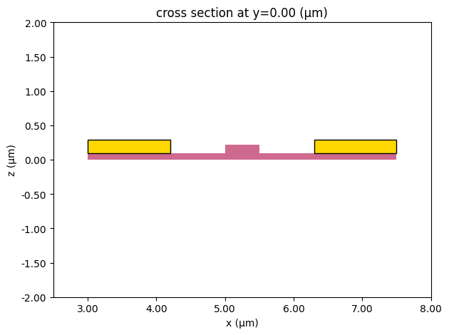
Before extruding any carrier profile, we build a small 2D test layout that includes Si, doped masks, and contacts. Plotting the resulting structures is a quick way to confirm that the mask layers and extrusion specs are wired correctly.
[8]:
c = pf.Component("Extrusion test", technology=tech)
c.add(
    "Si Slab",
    pf.Rectangle((3, -1), (7.5, 1)),
    "Si",
    pf.Rectangle((5, -1), (5.5, 1)),
    "Si n",
    pf.Rectangle((4.2, -1), (5.25, 1)),
    "Si p",
    pf.Rectangle((5.25, -1), (6.3, 1)),
    "Si n++",
    pf.Rectangle((3, -1), (4.2, 1)),
    "Si p++",
    pf.Rectangle((6.3, -1), (7.5, 1)),
    "Contact",
    pf.Rectangle((3, -1), (4.2, 1)),
    pf.Rectangle((6.3, -1), (7.5, 1)),
)

c.add_model(pf.Tidy3DModel(medium=sio2["electrical"].optical))

# Visual sanity check: 2D cross-section plot of the generated 3D structures.
pf.tidy3d_plot(c, y=0, plot_type="structures", frequency=10e9)
plt.xlim(2.5, 8)
plt.ylim(-2, 2)
plt.show()
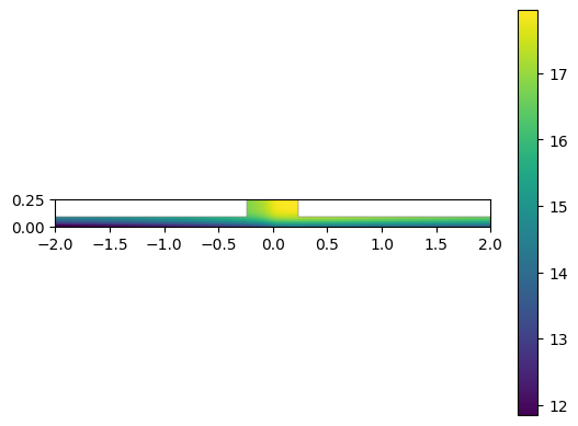
Carrier density profile (2D)
In many workflows you already have a donor/acceptor distribution from:
TCAD / process simulation
Measured sheet resistance / implant models
A library of standard implant steps
For this example we generate a synthetic 2D profile so the rest of the pipeline is self-contained.
Conventions used below
xis the lateral coordinate across the waveguide.zis the vertical coordinate (depth).n_a(x, z)is the acceptor density (p-type).n_d(x, z)is the donor density (n-type).
The profile is then extruded along a pf.Path in a later section.
[9]:
def f(x):
    """A smooth lateral profile used to separate p/n regions.

    This is a synthetic function for demonstration; replace with your imported data/model.
    """

    return 0.5 * (1 + 2 * np.arctan(x * 20) / np.pi) / (x**2 + 1)


def g(z):
    """A vertical (depth) profile envelope used for the implant distribution."""

    return np.exp(-(((z - 0.25) / 0.15) ** 4))


# Create a 2D grid for (x, z) and build donor/acceptor densities.
x, z = np.mgrid[-2:2:161j, 0:0.25:11j]

# Simple waveguide region mask (again: illustrative).
wg_mask = (abs(x) < 0.25) + (z < 0.09)

# Acceptors on +x, donors on -x (symmetry chosen for a junction-like profile).
n_a = 1e18 * f(x) * g(z) * wg_mask
n_d = 1e18 * f(-x) * g(z) * wg_mask


# Plot the acceptor profile on a log scale.
with np.errstate(divide="ignore"):
    plt.imshow(
        np.log10(n_a.T),
        origin="lower",
        extent=(x[0, 0], x[-1, -1], z[0, 0], z[-1, -1]),
    )
plt.colorbar()
plt.show()
Simple component (a pf.Path waveguide)
To demonstrate extrusion along a curved structure, we construct a simple waveguide bend using Path class.
Why pf.Path?
It provides a continuous centerline parameterization.
It can be interpolated densely, giving the local tangent/normal direction needed to map the 2D profile onto global coordinates.
The same idea generalizes to other parameterized geometries (rings/disks, etc.) where you can write down the coordinate transform.
[10]:
component = pf.Component("Doped bend")

# Define the waveguide centerline as a path.
# (This could be any geometry expressible as a `pf.Path`.)
path = pf.Path((0, 0), 0.5)
path.segment((1, 0))
path.turn(angle=90, radius=12, euler_fraction=0.5)
path.segment((0, 1), relative=True)

# Add core + slab.
component.add("Si", path)
component.add("Si Slab", path.updated_copy(width=5))

# Add doping mask layers as offset/width variants of the same path.
# These will be turned into 3D extrusions by the technology mapping configured earlier.
component.add("Si n", path.updated_copy(width=0.5, offset=0.25))
component.add("Si n++", path.updated_copy(width=1.5, offset=1.25))
component.add("Si p", path.updated_copy(width=0.5, offset=-0.25))
component.add("Si p++", path.updated_copy(width=1.5, offset=-1.25))

# Add an optical port so we can run a mode solve on the cross-section.
component.add_port(component.detect_ports(["Rib_TE_1550_500"]))

component
[10]:

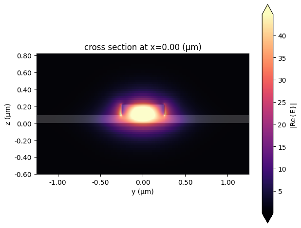
Optional: optical mode sanity check
This step is not required for doping extrusion, but it’s a useful validation that the cross-section + port definition are consistent with the technology stack (you should see a reasonable guided mode).
[11]:
mode_solver = pf.port_modes(
    component.ports["P0"],
    frequencies=[pf.C_0 / 1.55],
    mesh_refinement=40,
    group_index=True,
)

mode_solver.plot_field("E", mode_index=0, f=pf.C_0 / 1.55)

mode_solver.data.to_dataframe()
Uploading task 'Mode-ModeSolver…'Progress: 0% -
Starting task 'Mode-ModeSolver': https://tidy3d.simulation.cloud/workbench?taskId=mo-a577975e-f0dc-419e-a9a8-9603d797a782
Downloading data from 'Mode-ModeSolver'…
Progress: 100%
[11]:
| wavelength | n eff | k eff | loss (dB/cm) | TE (Ey) fraction | wg TE fraction | wg TM fraction | mode area | group index | dispersion (ps/(nm km)) | ||
|---|---|---|---|---|---|---|---|---|---|---|---|
| f | mode_index | ||||||||||
| 1.934145e+14 | 0 | 1.55 | 2.565038 | 0.0 | 0.0 | 0.986713 | 0.868478 | 0.802896 | 0.203597 | 3.888073 | -1534.852659 |
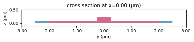
Generate a reference Tidy3D structure list
PhotonForge can produce a Tidy3D simulation object from the component + technology. Here we generate a reference simulation mainly to access sim.structures, which we will later update to include spatially varying doping.
[12]:
sim = pf.Tidy3DModel(medium=sio2["electrical"].optical).get_simulations(
    component, frequencies=[10e9]
)

ax = sim.plot_structures(x=0.001)
ax.set_xlim(-3, 3)
ax.set_ylim(-0.1, 0.5)
plt.show()
Generate the 3D doping distribution
Now we take the 2D cross-section profiles n_a(x, z) and n_d(x, z) and extrude them along the waveguide path.
Coordinate frames (what “extrusion” means here)
The 2D data lives in a local cross-section frame:
x: lateral coordinate across the waveguide (left/right)z: vertical coordinate (depth)
The waveguide is described by a centerline
pf.Pathin the chip plane (globalx,y).
At each point along the path we compute an in-plane moving frame:
tangent
t = (t_x, t_y)(from the path gradient)normal
n = (-t_y, t_x)(perpendicular to the tangent)
Then a local point (x_local, z_local) maps to global coordinates as:
(x_global, y_global) = pos_xy + x_local * nz_global = z_local
Voxelization strategy
Because the final data must be attached to a simulator as a 3D grid, we:
define a global voxel grid
(xs, ys, zs)over the component bounds,sample many
pos_xylocations along the path,“splat” the full
n_a(x,z)/n_d(x,z)cross-section into the nearest voxel columns,and average when multiple splats hit the same voxel.
This same strategy works for other spatial fields (temperature, stress, index perturbations) as long as you can define a local→global coordinate transform.
Voxelize the 2D cross-section into a 3D field along the path
This cell implements the extrusion algorithm: it samples points along the pf.Path, maps the local cross-section coordinate x into global (x,y) using the local normal direction, and accumulates n_a / n_d onto a global (xs,ys,zs) voxel grid.
[13]:
(xmin, ymin), (xmax, ymax) = component.bounds()
num_pts = 500
xs = np.linspace(xmin, xmax, num_pts)
ys = np.linspace(ymin, ymax, num_pts)
zs = z[0]
n_as = np.zeros((xs.size, ys.size, zs.size))
n_ds = np.zeros((xs.size, ys.size, zs.size))
counts = np.zeros((xs.size, ys.size, zs.size))
dx = xs[1] - xs[0]
dy = ys[1] - ys[0]
for pos, _, _, gradient in zip(
*path.interpolate(np.linspace(0, path.length(), 10 * num_pts))
):
# `gradient` is the local tangent direction t = (t_x, t_y).
# The in-plane normal is n = (-t_y, t_x).
#
# Map each lateral cross-section coordinate x_local into global coordinates:
# (x_global, y_global) = pos_xy + x_local * n
x_local = x[:, 0]
xt = pos[0] - gradient[1] * x_local - xmin
yt = pos[1] + gradient[0] * x_local - ymin
# Convert global coordinates into voxel indices.
i = np.clip((xt / dx).round().astype(int), 0, xs.size - 1).tolist()
j = np.clip((yt / dy).round().astype(int), 0, ys.size - 1).tolist()
# Advanced indexing note:
# `n_as[i, j, :]` has shape (len(x_local), len(zs)) and matches `n_a`'s (x,z) grid.
n_as[i, j, :] += n_a
n_ds[i, j, :] += n_d
counts[i, j, :] += 1
# Avoid division by zero when averaging.
counts = np.clip(counts, 1, None)
n_as /= counts
n_ds /= counts
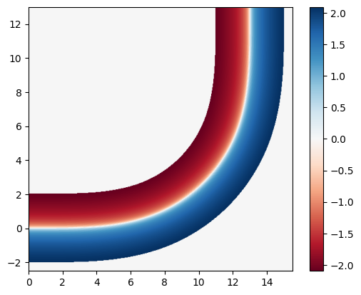
# Quick visualization: net doping sign on the z=0 slice (log-scaled donors minus acceptors).
plt.imshow(
np.log10(n_ds[:, :, 0].T + 1e-10) - np.log10(n_as[:, :, 0].T + 1e-10),
origin="lower",
extent=(xmin, xmax, ymin, ymax),
cmap="RdBu",
)
plt.colorbar()
plt.show()
Generalizing the extrusion idea
Extruding a 2D field over a 3D structure is mainly about:
Defining the coordinate transform from a local cross-section frame to global coordinates
Sampling densely enough to avoid holes/aliasing in the final voxel grid
Any waveguide described as a pf.Path can use the algorithm above.
For rings/disks (or other analytical shapes), you can derive the transform directly from geometry and skip path interpolation entirely.
Attach the 3D doping to the semiconductor medium
We wrap the voxelized arrays n_d(x,y,z) and n_a(x,y,z) into td.SpatialDataArray objects and inject them into the semiconductor charge model. This produces a new MultiPhysicsMedium named “Doped Si” with spatially varying donor/acceptor densities.
[14]:
donors_array = td.SpatialDataArray(data=n_ds, coords={"x": xs, "y": ys, "z": zs})

acceptors_array = td.SpatialDataArray(data=n_as, coords={"x": xs, "y": ys, "z": zs})

doped_si = td.MultiPhysicsMedium(
    optical=td.Medium(permittivity=11.7),
    charge=charge_spec.updated_copy(N_d=donors_array, N_a=acceptors_array),
    name="Doped Si",
)
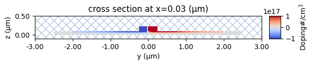
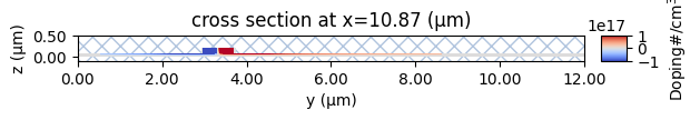
Here we swap the placeholder “Doped Si” medium inside the generated sim.structures with the updated one (containing spatially varying N_d(x,y,z) / N_a(x,y,z)), then plot a couple of cross-sections of the resulting doping field.
[15]:
structures = []
for s in sim.structures:
    if s.medium.name == "Doped Si":
        s = s.updated_copy(medium=doped_si)
    structures.append(s)

scene = td.Scene(structures=structures, medium=sio2["electrical"])

doping_range = [-1e17, 1e17]

scene.plot_structures_property(
    x=xs[1], property="doping", limits=doping_range, hlim=(-3, 3), vlim=(-0.1, 0.5)
)

scene.plot_structures_property(
    x=xs[350], property="doping", limits=doping_range, hlim=(0, 12), vlim=(-0.1, 0.5)
)

plt.show()
Next steps
At this point the 3D donor/acceptor distributions are embedded in the Tidy3D structures.
Typical follow-ups:
Run a charge simulation to compute carrier distributions under bias
Use the resulting perturbation in an FDTD simulation (e.g., resonance shift / phase shift)
Sweep process parameters (junction offset, peak concentration, anneal spread, etc.) by regenerating the 2D profile and repeating the extrusion
If you already have TCAD output, replace the synthetic n_a / n_d arrays with your imported data (making sure the coordinate convention matches) and keep the rest of the pipeline the same.