
Custom Component Library

PhotonForge components are PCells (parameterized cells). They can be real or virtual, and they can be hierarchical.
Models: simulation, analytical equations, or measured experimental data
Ports: optical, electrical, or virtual
Layout import: Cadence OpenAccess database or GDS/OASIS files
Getting Started
Load the technology.
[1]:
%%capture
# Load the technology stack and helper imports
%run Loading_Technology.ipynb
# Reduce Tidy3D logging noise in the notebook
td.config.logging.level = "ERROR"
We import a few utilities, start the interactive viewer, and set technology-specific defaults (optical port spec, default bend radius, and Tidy3D mesh refinement).
[2]:
import warnings
from photonforge.live_viewer import LiveViewer
from photonforge.stencil import as_component
# Suppress warnings about unmatched terminals and ports
warnings.filterwarnings(
"ignore", message="Terminal.*does not match any reference terminals"
)
warnings.filterwarnings(
"ignore", message=".*not connected and will be ignored.*"
)
viewer = LiveViewer()
port_spec = tech.ports["TE_1550_500"] # optical port definition
pf.config.default_kwargs["port_spec"] = port_spec
pf.config.default_kwargs["radius"] = 5 # default bend radius (µm)
pf.config.default_kwargs["euler_fraction"] = 0.5
pf.config.default_mesh_refinement = 12 # default mesh refinement for Tidy3D simulations
rib = tech.ports["Rib_TE_1550_500"]
LiveViewer started at http://localhost:41777
We set up the wavelength/frequency grid for frequency sweeps and define a carrier point (\(\lambda_0\), \(f_0\)) used for single-frequency mode solves.
We also define a nominal propagation loss model (used later in analytical / compact models) so that device responses include realistic insertion loss.
[3]:
wavelengths = np.linspace(1.543, 1.558, 201)
lambda0 = 1.55
freqs = pf.C_0 / wavelengths
freq0 = pf.C_0 / lambda0
# Waveguide properties
propagation_loss = 3.0 / 10000.0 # propagation loss: 3 dB/cm (converted to dB/µm)
We solve for the waveguide eigenmodes at the carrier wavelength to extract effective index and group index values used later for analytical models.
The next cell runs the mode solver for the default strip waveguide, and the following cell repeats the same workflow for the rib waveguide.
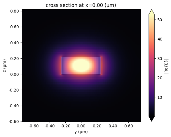
[4]:
# Solve the strip waveguide mode at the carrier frequency
mode_solver = pf.port_modes(port_spec, [freq0], mesh_refinement=50, group_index=True)
# Plot the mode electric-field profile
mode_solver.plot_field("E", mode_index=0, f=freq0)
# Extract the fundamental-mode effective and group indices
n_eff = mode_solver.data.n_eff.isel(mode_index=0).item()
n_group = mode_solver.data.n_group.isel(mode_index=0).item()
mode_solver.data.to_dataframe()
Uploading task 'Mode-ModeSolver…'
Starting task 'Mode-ModeSolver': https://tidy3d.simulation.cloud/workbench?taskId=mo-42069232-f4e2-44f5-b260-e447eece9038
Downloading data from 'Mode-ModeSolver'…
Progress: 100%
[4]:
| wavelength | n eff | k eff | loss (dB/cm) | TE (Ey) fraction | wg TE fraction | wg TM fraction | mode area | group index | dispersion (ps/(nm km)) | ||
|---|---|---|---|---|---|---|---|---|---|---|---|
| f | mode_index | ||||||||||
| 1.934145e+14 | 0 | 1.55 | 2.443192 | 0.0 | 0.0 | 0.983501 | 0.764069 | 0.81791 | 0.190715 | 4.187462 | 515.572825 |
[5]:
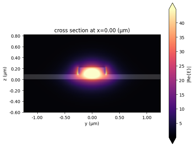
# Solve the rib waveguide mode at the carrier frequency
mode_solver_rib = pf.port_modes(rib, [freq0], mesh_refinement=50, group_index=True)
# Plot the mode electric-field profile
mode_solver_rib.plot_field("E")
# Extract the fundamental-mode group index
n_group_rib = mode_solver_rib.data.n_group.isel(mode_index=0).item()
# Extract the fundamental-mode effective index
n_eff_rib = mode_solver_rib.data.n_eff.isel(mode_index=0).item()
Uploading task 'Mode-ModeSolver…'Progress: 0% -
Starting task 'Mode-ModeSolver': https://tidy3d.simulation.cloud/workbench?taskId=mo-c79e3586-6770-4cc7-88e8-337b5ab8ec50
Downloading data from 'Mode-ModeSolver'…
Progress: 100%
Edge Coupler
Edge couplers provide efficient fiber-to-chip coupling by expanding the guided mode near the facet to better match the fiber mode. In this notebook we use an angled inverse-taper edge coupler geometry that is parameterized for reuse and quick sweeps.
Design Tip: High coupling efficiency requires matching the mode profiles of the chip and the fiber. We use a lensed fiber (2.5 µm spot diameter) to focus the light, while simultaneously using a narrow inverse taper tip (150 nm) to expand the waveguide mode. A long adiabatic taper is used to transition seamlessly between the standard 500 nm waveguide and the narrow tip without scattering losses.
To minimize back-reflections (return loss), the waveguide tip is angled (typically 7°–15°). A straight facet would reflect light directly back into the laser, causing instability. The angle ensures that any reflected light is steered away from the guided mode and radiated into the cladding. Return loss can be further reduced by filling the gap with an index-matching material (such as epoxy or fluid), which minimizes Fresnel reflections at the facet.
See the PhotonForge edge coupler example for more details.
[6]:
@pf.parametric_component(name_prefix="Angled Fiber")
def angled_edge_coupler(
*,
width_tip=0.1, # Width of the taper tip (µm)
length_taper=10, # Length of the adiabatic taper (µm)
angle_taper=7, # Angle of the waveguide facet (degrees)
waist_radius=2.0, # Mode field radius of the fiber (µm)
fiber_distance=3.0, # Distance from facet to fiber (µm)
angle_fiber=10.2, # Angle of fiber incidence (degrees)
trench_layer="Deep Trench", # Layer for the etch opening
):
"""
Creates an angled inverse taper edge coupler for low-reflection fiber coupling.
Parameters:
width_tip (float): Width of the waveguide tip (µm).
length_taper (float): Length of the adiabatic taper (µm).
angle_taper (float): Angle of the waveguide facet (degrees).
waist_radius (float): Mode field radius of the coupling fiber (µm).
fiber_distance (float): Distance between the fiber and the facet (µm).
angle_fiber (float): Angle of the fiber incidence (degrees).
trench_layer (str): Layer name for the deep trench opening.
Returns:
Component: The edge coupler component with optical ports.
"""
# Get waveguide width and silicon thickness from the technology
port_spec = tech.ports["TE_1550_500"]
core_width, _ = port_spec.path_profile_for("Si")
core_thickness = tech.parametric_kwargs["si_thickness"]
# Unit vectors for the taper direction and fiber axis (degrees -> radians)
v_taper = np.array(
(np.cos(angle_taper / 180 * np.pi), np.sin(angle_taper / 180 * np.pi))
)
v_fiber = np.array(
(np.cos(angle_fiber / 180 * np.pi), np.sin(angle_fiber / 180 * np.pi))
)
# Build the silicon inverse taper
endpoint = pf.snap_to_grid(length_taper * v_taper)
taper = (
pf.Path(-waist_radius * v_taper, width_tip)
.segment((0, 0))
.segment(endpoint, core_width)
)
# Taper endpoint after a small bend to guarantee that the waveguide port
# grid-aligned
if angle_taper > 0:
radius = 5
endpoint = pf.snap_to_grid(
endpoint + radius * np.array((abs(v_taper[1]), 1 - v_taper[0]))
)
base = 90 if angle_taper > 0 else -90
taper.arc(90 + angle_taper, 90, radius, endpoint=endpoint)
component = pf.Component(technology=siepic.ebeam())
# Define the fiber port position from distance and fiber angle
fiber_center = -fiber_distance * v_fiber
port_fiber = pf.GaussianPort(
center=(fiber_center[0], fiber_center[1], core_thickness / 2),
input_vector=(v_fiber[0], v_fiber[1], 0),
waist_radius=waist_radius,
polarization_angle=0, # TE polarization
)
# Define the on-chip port at the end of the taper
port_waveguide = pf.Port(endpoint, 180, port_spec)
component.add_port([port_fiber, port_waveguide])
# Add taper and trench opening near the facet
# The size of Trench defines the boundary of the simulation so it is important to be sufficiently large
component.add(
"Si",
taper,
trench_layer,
pf.Rectangle(
(-fiber_distance - waist_radius, -5 * waist_radius),
(
0,
max(
5 * waist_radius,
port_waveguide.center[1] + port_spec.width / (2 * v_taper[0]),
),
),
),
)
model = pf.Tidy3DModel()
component.add_model(model, "Tidy3D")
return component
[7]:
angle_fiber = 15 # degrees
# Estimate taper angle using Snell's law (n ≈ 1.45)
angle_taper = np.arcsin(np.sin(angle_fiber / 180 * np.pi) / 1.45) / np.pi * 180
print(f"Taper angle: {angle_taper}°")
edge_coupler = angled_edge_coupler(
width_tip=0.15,
length_taper=25,
angle_taper=angle_taper,
waist_radius=2.5 / 2,
fiber_distance=3,
angle_fiber=angle_fiber,
)
# Visualize the geometry
viewer(edge_coupler)
Taper angle: 10.282162084410936°
[7]:

[8]:
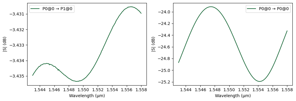
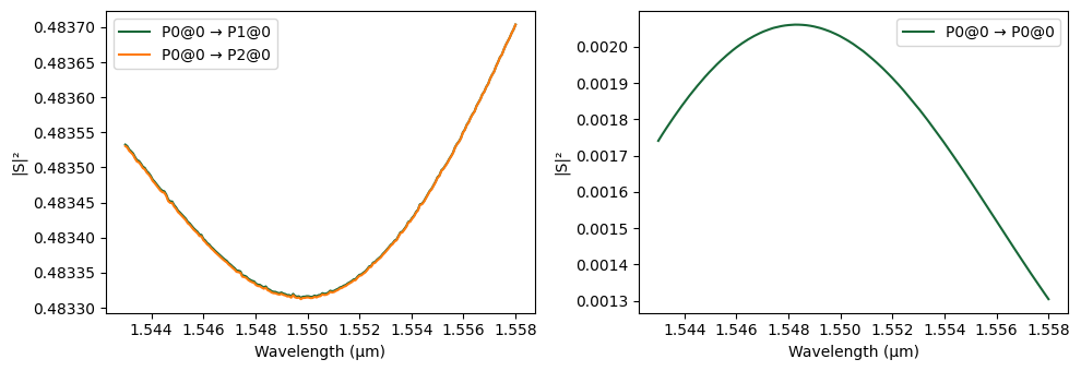
# Simulate and plot the edge-coupler S-matrix
s_matrix_ec = edge_coupler.s_matrix(freqs)
_ = pf.plot_s_matrix(s_matrix_ec, y="dB", input_ports=["P0"])
Uploading task 'P0@0…'
Uploading task 'P1@0…'
Starting task 'P0@0': https://tidy3d.simulation.cloud/workbench?taskId=fdve-85119ede-f9e6-4450-b3e8-6178786a9b2f
Downloading data from 'P0@0'…
Starting task 'P1@0': https://tidy3d.simulation.cloud/workbench?taskId=fdve-4106b825-50d7-4f3d-8ca9-f8e59131ba03
Downloading data from 'P1@0'…
Progress: 100%
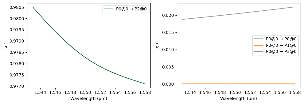
Monitor Tap
This section defines a weak directional coupler used as a monitor tap (99:1) to sample a small fraction of the optical power for calibration and control.
Design Tip: To achieve a weak coupling ratio (1%), we must limit the power transfer between waveguides. This is typically done by increasing the gap or decreasing the coupling length.
Because the coupling coefficient is sensitive to geometry, the precise parameters are best found via a parameter sweep. A common approach is to fix the gap (e.g., a fabrication-safe value like 300 nm) and sweep the coupling length to dial in the exact 1% split.
[9]:
@pf.parametric_component(name_prefix="Monitor Tap")
def monitor_tap(
*,
coupling_gap=0.3, # gap between waveguides (µm)
coupling_length=2.4, # coupling region length (µm)
coupling_offset=5, # S-bend offset for coupler (µm)
s_bend_length=20, # drop-arm S-bend length (µm)
s_bend_offset=10, # drop-arm offset (µm)
):
"""
99:1 S-bend directional coupler.
99% transmission on the through port (P0 -> P1).
1% coupling to the tap port (P0 -> P2, routed via S-bend).
"""
wg_width, _ = port_spec.path_profile_for("Si")
# Create the directional coupler
tidy3d_model = pf.Tidy3DModel(
verbose=True,
port_symmetries=[
("P1", "P0", "P3", "P2"),
("P2", "P3", "P0", "P1"),
("P3", "P2", "P1", "P0"),
],
)
coupler = pf.parametric.s_bend_coupler(
coupling_distance=wg_width + coupling_gap,
coupling_length=coupling_length,
s_bend_offset=coupling_offset,
model=tidy3d_model,
)
# Create an S-bend to route the monitor port
s_bend = pf.parametric.s_bend(
length=s_bend_length,
offset=s_bend_offset,
model=pf.WaveguideModel(),
)
# Assemble the component via a netlist
netlist = {
"instances": {"COUPLER": coupler, "S_BEND": s_bend},
"connections": [
(("S_BEND", "P0"), ("COUPLER", "P3")),
],
"ports": [
("COUPLER", "P0"), # Input
("COUPLER", "P2"), # Through (99%)
("S_BEND", "P1"), # Monitor tap (1%)
("COUPLER", "P1"), # Drop (unused)
],
"models": [pf.CircuitModel()],
}
return pf.component_from_netlist(netlist)
pm = monitor_tap()
viewer(pm)
[9]:

[10]:
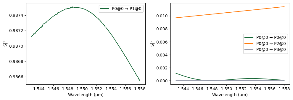
# Simulate and plot the power monitor S-matrix
s_matrix_pm = pm.s_matrix(freqs)
_ = pf.plot_s_matrix(s_matrix_pm, input_ports=["P0"])
Uploading task 'P0@0…'
Uploading task 'Mode-StripTE1550nmw500nm…'
Starting task 'P0@0': https://tidy3d.simulation.cloud/workbench?taskId=fdve-1b4d8156-85f3-4129-8832-b61c8ee0c0a5
Starting task 'Mode-StripTE1550nmw500nm': https://tidy3d.simulation.cloud/workbench?taskId=mo-79cc3145-e1c1-4ade-8020-15fca2056566
Downloading data from 'P0@0'…
Downloading data from 'Mode-StripTE1550nmw500nm'…
Progress: 100%
Monitor Photodiode
The monitor photodiode is an integrated detector used to convert a fraction of the optical signal into an electrical current for power tracking. This component is modeled after the Keysight N1030A specifications, providing a high-bandwidth (65 GHz) response for real-time monitoring of signal integrity and link performance.
[11]:
@pf.parametric_component(name_prefix="Monitor PD")
def monitor_photodiode(
*,
width=100, # detector box size (µm)
pad_width=25, # metal pad size (µm)
):
"""
Monitor photodiode with a realistic 65 GHz detector model.
Based on Keysight N1030A specifications (65 GHz unamplified module).
Includes an optical input port and electrical terminals for readout.
"""
c = pf.Component()
# Photodetector active area (black box)
rect = pf.Rectangle(center=(0, 0), size=(width, width))
c.add("Dream Photonics Black Box-Not Fabricated", rect)
# Add a text label
text_comp = as_component(
layer="Text",
stencil="text",
text_string="Monitor PD",
size=10.0,
)
text_ref = pf.Reference(text_comp, origin=(-width / 4, 0))
c.add_reference(text_ref)
# Optical input port
port_in = pf.Port(
center=(-width / 2.0, 0),
spec=port_spec,
input_direction=0,
)
# Electrical output port
port_out = pf.Port(
center=(width / 2.0, 0),
spec=pf.virtual_port_spec(classification="electrical"),
input_direction=0,
)
c.add_port([port_in, port_out])
# Metal pads for electrical readout (GSG configuration)
rect_signal = pf.Rectangle(center=(0, 0), size=(pad_width, pad_width))
rect_signal.y_min = pad_width / 2.0
rect_signal.x_max = width / 2.0
rect_ground = rect_signal.copy()
rect_ground.y_max = -pad_width / 2.0
c.add("M2_router", rect_signal, rect_ground)
# Electrical terminals
signal_pad = pf.Terminal("M2_router", rect_signal.copy())
ground_pad = pf.Terminal("M2_router", rect_ground.copy())
c.add_terminal([signal_pad, ground_pad])
# Use one-port termination model to enable frequency domain simulations
detector_model = pf.TerminationModel()
# Photodiode time-domain model (Keysight N1030A, 65 GHz)
detector_model.time_stepper = pf.PhotodiodeTimeStepper(
responsivity=0.85, # A/W (InGaAs at 1550 nm)
gain=50.0, # V/A (50 Ω load)
saturation_current=6.8e-3, # A (8 mW max input)
dark_current=10e-9, # A (10 nA typical)
thermal_noise=3.3e-22, # A^2/Hz (Johnson noise)
filter_frequency=65e9, # Hz (65 GHz bandwidth)
roll_off=2,
)
c.add_model(detector_model, "Photodiode")
return c
pd = monitor_photodiode()
viewer(pd)
[11]:

Y-Splitter
This section defines a splitter/combiner for distributing optical power between one input and two outputs. We use a PDK component.
Design Tip: One of the most robust approaches for low-loss splitting is an adiabatic Y-junction. By gradually expanding the input waveguide, the fundamental mode evolves smoothly into the two output arms with minimal scattering or reflection.
Fabrication Note: Because perfectly sharp tips are impossible to manufacture, a “healed” geometry (blunted tip) is used to ensure the gap size respects the foundry’s minimum feature size (e.g., 60 nm) while maintaining adiabatic behavior.
[12]:
# Load and visualize an adiabatic Y-junction splitter PCell
splitter = siepic.component("ebeam_y_1550")
viewer(splitter)
[12]:

[13]:
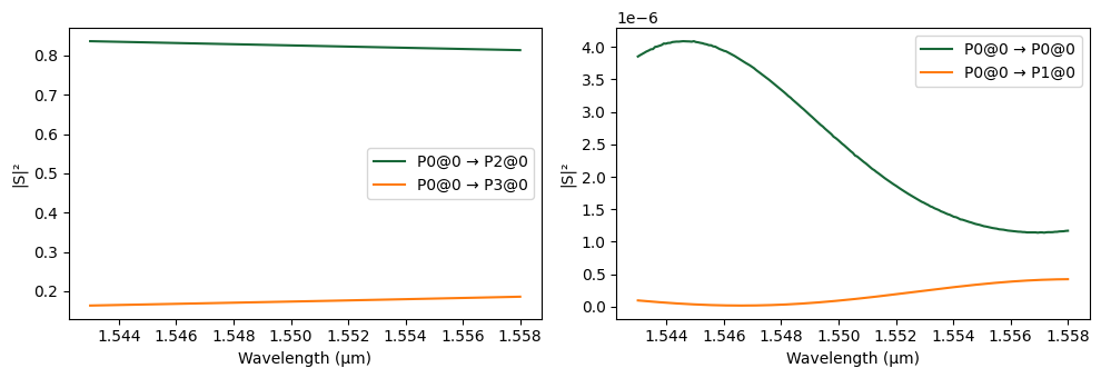
# Simulate and plot the splitter S-matrix
s_matrix_splitter = splitter.s_matrix(freqs)
_ = pf.plot_s_matrix(s_matrix_splitter, input_ports=["P0"])
# Add the simulation results as a DataModel to avoid future FDTD simulations for different frequencies
# splitter.add_model(pf.DataModel(s_matrix_splitter))
Uploading task 'P0@0…'
Uploading task 'P1@0…'
Starting task 'P0@0': https://tidy3d.simulation.cloud/workbench?taskId=fdve-88e8de5b-5590-4517-8ac1-241367f621b0
Starting task 'P1@0': https://tidy3d.simulation.cloud/workbench?taskId=fdve-bc647359-65d2-4ada-a708-847109dbf4b8
Downloading data from 'P0@0'…
Downloading data from 'P1@0'…
Progress: 100%
Directional Couplers for the MUX
We will build a 4-channel MUX using a dual-ring resonator.
Reference:
De Heyn, P., et al., “Fabrication-Tolerant Four-Channel Wavelength-Division-Multiplexing Filter Based on Collectively Tuned Si Microrings,” Journal of Lightwave Technology, 2013 31 (16), 2785–2792, doi: 10.1109/JLT.2013.2273391.
First, we define a directional coupler component. A grid_spec of 25 is used to ensure the high mesh accuracy necessary for simulating resonant structures.
[14]:
@pf.parametric_component(name_prefix="Directional Coupler")
def directional_coupler(
*,
coupling_gap=0.340, # gap between waveguides (µm)
radius=5, # bend radius (µm)
coupling_length=9, # coupling region length (µm)
heater_width=4.0, # heater width (µm)
):
"""
Tunable directional coupler with thermal heaters.
Used for:
- Ring-to-ring coupling in add-drop filters
- Bus-to-ring coupling in resonators
"""
wg_width, _ = port_spec.path_profile_for("Si")
coupling_distance = wg_width + coupling_gap
component = pf.parametric.dual_ring_coupler(
coupling_distance=coupling_distance,
radius=radius,
coupling_length=coupling_length,
model=pf.Tidy3DModel(
grid_spec=25,
port_symmetries=[
("P1", "P0", "P3", "P2"),
("P2", "P3", "P0", "P1"),
("P3", "P2", "P1", "P0"),
],
),
)
left_corner = component.ports["P1"].center - (
0,
heater_width / 2 + radius + coupling_distance / 2,
)
right_corner = component.ports["P3"].center + (
0,
heater_width / 2 - radius - coupling_distance / 2,
)
component.add("M1_heater", pf.Rectangle(left_corner, right_corner))
return component
Two-Ring Resonator Filter
This section builds a two-ring add–drop resonator filter (2RR) as a reusable WDM building block, including heaters for thermal tuning.
Design Tip: To achieve a flat-top (maximally flat) passband in a two-ring add–drop filter (with identical rings), choose the coupling gaps such that the bus-to-ring and ring-to-ring coupling coefficients satisfy the following synthesis relation:
where:
\(\kappa_{\text{ext}}\) — bus-to-ring (external) power coupling coefficient (\(\kappa_{\text{ext}} \approx 0.2\) in our design)
\(\kappa_{\text{int}}\) — ring-to-ring (internal) power coupling coefficient (\(\kappa_{\text{int}} \approx 0.02\) in our design)
This condition ensures a maximally flat spectral response by properly balancing external and internal coupling strengths.
[15]:
dc_rr = directional_coupler(coupling_gap=0.348)
viewer(dc_rr)
[15]:

[16]:
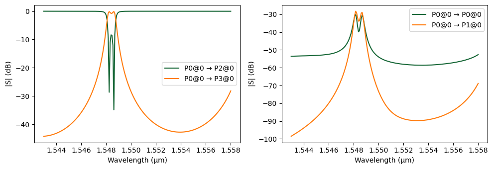
# Run a finer wavelength sweep to visualize the 2RR filter response
s_matrix_rr = dc_rr.s_matrix(freqs, model_kwargs={"inputs": ["P0"]})
_ = pf.plot_s_matrix(s_matrix_rr, input_ports=["P0"])
p3 = np.abs(s_matrix_rr[("P0@0", "P3@0")]) ** 2
p2 = np.abs(s_matrix_rr[("P0@0", "P2@0")]) ** 2
print(
f"The internal coupling ratio at the center wavelength is: {p3[len(freqs)//2]/p2[len(freqs)//2]:.4f}"
)
Uploading task 'P0@0…'
Starting task 'P0@0': https://tidy3d.simulation.cloud/workbench?taskId=fdve-f4a63f36-6b75-4f20-b962-7fec5d3cf187
Downloading data from 'P0@0'…
Progress: 100%
The internal coupling ratio at the center wavelength is: 0.0210
[17]:
dc_br = directional_coupler(coupling_gap=0.22)
viewer(dc_br)
[17]:

[18]:
s_matrix_br = dc_br.s_matrix(freqs, model_kwargs={"inputs": ["P0"]})
_ = pf.plot_s_matrix(s_matrix_br, input_ports=["P0"])
p3 = np.abs(s_matrix_br[("P0@0", "P3@0")]) ** 2
p2 = np.abs(s_matrix_br[("P0@0", "P2@0")]) ** 2
print(
f"The external coupling ratio at the center wavelength is: {p3[len(freqs)//2]/p2[len(freqs)//2]:.3f}"
)
Uploading task 'P0@0…'
Starting task 'P0@0': https://tidy3d.simulation.cloud/workbench?taskId=fdve-c2b22064-432e-4cd0-ade8-902c6e3303dc
Downloading data from 'P0@0'…
Progress: 100%
The external coupling ratio at the center wavelength is: 0.211
[19]:
@pf.parametric_component(name_prefix="2RR Filter")
def filter_2rr(
*,
coupling_length=9.0, # coupling length (µm)
radius=5.0, # ring radius (µm)
rr_gap=0.348, # ring-to-ring gap (µm)
br_gap=0.220, # bus-to-ring gap (µm)
pad_width=10, # bond pad width (µm)
):
"""
Two-ring resonator (2RR) add-drop filter.
Architecture:
- Two rings coupled via a ring-to-ring coupler.
- Each ring coupled to the bus waveguide.
- Thermal tuning via heaters.
"""
# Create coupler components
dc_2rr = directional_coupler(
coupling_gap=rr_gap,
radius=radius,
coupling_length=coupling_length,
)
dc_2br = directional_coupler(
coupling_gap=br_gap,
radius=radius,
coupling_length=coupling_length,
)
# Create helper components
bend = pf.parametric.bend() # 90 deg bend (default)
wg = pf.parametric.straight(length=60)
# Assemble the 2RR filter via a netlist
netlist_2rr = {
"instances": {
"bus_coupler0": dc_2br,
"bus_coupler1": dc_2br,
"ring_coupler0": dc_2rr,
"bend0": bend,
"bend1": bend,
"wg0": wg,
"wg1": wg,
"wg2": wg,
},
"connections": [
(("ring_coupler0", "P0"), ("bus_coupler0", "P1")),
(("bus_coupler1", "P3"), ("ring_coupler0", "P1")),
(("bend0", "P0"), ("bus_coupler1", "P2")),
(("bend1", "P1"), ("bus_coupler1", "P0")),
(("wg0", "P1"), ("bus_coupler0", "P0")),
(("wg1", "P1"), ("bend0", "P1")),
(("wg2", "P1"), ("bus_coupler0", "P2")),
],
"ports": [
("wg0", "P0"),
("wg1", "P0"),
("wg2", "P0"),
("bend1", "P0"),
],
"models": [pf.CircuitModel()],
}
two_rr = pf.component_from_netlist(netlist_2rr)
# Add bond pads for heater control (heater terminals)
p0_center = np.array(dc_2br.ports["P0"].center)
p3_center = np.array(dc_2br.ports["P3"].center)
bp1 = pf.Rectangle(center=p0_center, size=(pad_width, 2 * pad_width))
bp1.x_max = p0_center[0] + pad_width / 2.0 - 1.0
bp1.y_max = p0_center[1] - pad_width / 2.0
rect1 = pf.Rectangle(center=p0_center, size=(pad_width / 2.0, pad_width * 4))
rect1.x_max = bp1.x_max
rect1.y_min = bp1.y_max
bp2 = bp1.copy()
bp2.x_min = p3_center[0] - pad_width / 2.0 + 1.0
bp2.y_min = p3_center[1] + pad_width / 2.0 + 4 * radius
rect2 = rect1.copy()
rect2.x_min = bp2.x_min
rect2.y_max = bp2.y_min
two_rr.add("M2_router", bp1, rect1, bp2, rect2)
signal_pad = pf.Terminal("M2_router", bp1.copy())
ground_pad = pf.Terminal("M2_router", bp2.copy())
two_rr.add_terminal([signal_pad, ground_pad])
return two_rr
two_rr = filter_2rr()
viewer(two_rr)
[19]:

[20]:
s_matrix_2rr = two_rr.s_matrix(freqs, model_kwargs={"inputs": ["P0"]})
_ = pf.plot_s_matrix(s_matrix_2rr, y="dB", input_ports=["P0"])
Starting…
07:28:19 -03 Loading simulation from local cache. View cached task using web UI at 'https://tidy3d.simulation.cloud/workbench?taskId=fdve-c2b22064-432 e-4cd0-ade8-902c6e3303dc'.
Uploading task 'Mode-StripTE1550nmw500nm…'
Uploading task 'Mode-StripTE1550nmw500nm…'
07:28:20 -03 Loading simulation from local cache. View cached task using web UI at 'https://tidy3d.simulation.cloud/workbench?taskId=fdve-4577b3fb-868 7-4303-a941-9d907d5f945f'.
Uploading task 'Mode-StripTE1550nmw500nm…'
Uploading task 'Mode-StripTE1550nmw500nm…'
Uploading task 'Mode-StripTE1550nmw500nm…'
Starting task 'Mode-StripTE1550nmw500nm': https://tidy3d.simulation.cloud/workbench?taskId=mo-12d3db3d-9146-4834-ae13-d17070d0011b
Starting task 'Mode-StripTE1550nmw500nm': https://tidy3d.simulation.cloud/workbench?taskId=mo-7ec22c9b-4ba0-474f-bdf3-66cac44f9c55
Downloading data from 'Mode-StripTE1550nmw500nm'…
Starting task 'Mode-StripTE1550nmw500nm': https://tidy3d.simulation.cloud/workbench?taskId=mo-a9bea4b1-27c9-45a3-ba75-1f055995ea00
Downloading data from 'Mode-StripTE1550nmw500nm'…
Starting task 'Mode-StripTE1550nmw500nm': https://tidy3d.simulation.cloud/workbench?taskId=mo-40e12a40-d173-4327-a0c2-b81e39f923b7
Starting task 'Mode-StripTE1550nmw500nm': https://tidy3d.simulation.cloud/workbench?taskId=mo-da066e10-da93-4b50-aba2-14760d9f678a
Downloading data from 'Mode-StripTE1550nmw500nm'…
Downloading data from 'Mode-StripTE1550nmw500nm'…
Downloading data from 'Mode-StripTE1550nmw500nm'…
Progress: 100%
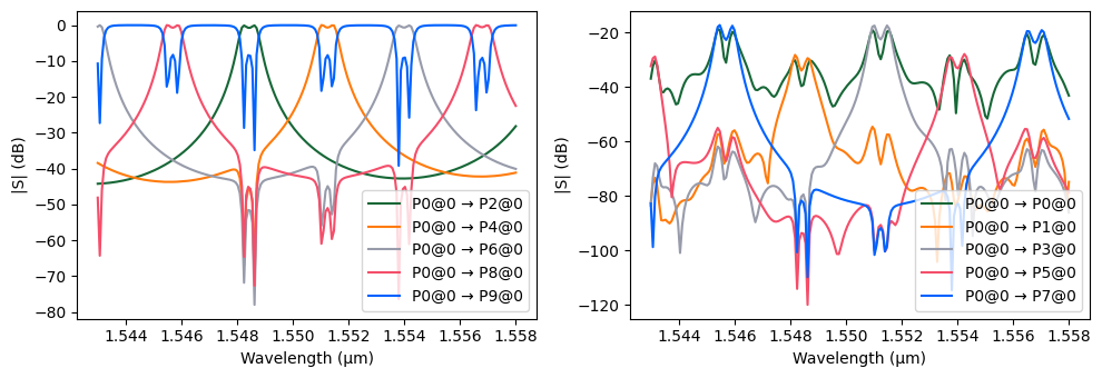
Four-Channel WDM
When cascading multiple resonator filters into a WDM, the ring free spectral range (FSR) and the desired channel spacing must be co-designed to avoid channel collisions and routing ambiguity.
Design Tip: WDM Channel Spacing & FSR
To create a 4-channel WDM, we stagger the resonance of each filter by 1/4 of the Free Spectral Range (FSR).
Theory:
Free Spectral Range (FSR): The frequency spacing between consecutive resonances is determined by the group index (\(n_g\)) and total ring perimeter (\(L\)):
\[FSR = \frac{\lambda^2}{n_g L}\]Channel Shift: We need to shift the resonance by \(1/4 \text{ FSR}\), which corresponds to a phase shift of \(\pi/2\). The required change in ring perimeter (\(\Delta L\)) is:
\[\Delta L_{perimeter} = \frac{\lambda}{4 n_{eff}}\]Since our parameterized
coupling_lengthadds to the ring twice (once per side), the requiredadded_lengthparameter is:\[\text{added\_length} = \frac{\lambda}{8 n_{eff}}\]
[21]:
L_ring = 2 * np.pi * 5 + 2 * 9 # approximate perimeter (µm)
# Compute the FSR and required resonance shift
fsr_nm = (lambda0**2) / (n_group * L_ring) * 1000
added_length = pf.snap_to_grid(lambda0 / (8 * n_eff))
print(f"Est. FSR: {fsr_nm:.1f} nm")
print(f"Required added_length: {added_length*1000:.1f} nm")
Est. FSR: 11.6 nm
Required added_length: 79.0 nm
[22]:
@pf.parametric_component(name_prefix="WDM 4ch")
def wdm_4channel(
*,
coupling_length=9.0, # base coupling length (µm)
added_length=added_length, # incremental length per channel (µm)
radius=5, # ring radius (µm)
):
"""
4-channel C-band WDM using cascaded 2RR filters.
Each 2RR uses a slightly different coupling length to tune the resonance
to a different wavelength.
"""
# Create four filters with incremental coupling lengths
two_rr_0 = filter_2rr(coupling_length=coupling_length, radius=radius)
two_rr_1 = filter_2rr(coupling_length=coupling_length + added_length, radius=radius)
two_rr_2 = filter_2rr(
coupling_length=coupling_length + 2 * added_length, radius=radius
)
two_rr_3 = filter_2rr(
coupling_length=coupling_length + 3 * added_length, radius=radius
)
# Output waveguide
wg = pf.parametric.straight(length=60)
# Netlist for 4-channel MUX
netlist = {
"instances": {
"2rr0": two_rr_0,
"2rr1": two_rr_1,
"2rr2": two_rr_2,
"2rr3": two_rr_3,
"wg": wg,
},
"connections": [
(("2rr1", "P1"), ("2rr0", "P3")),
(("2rr2", "P1"), ("2rr1", "P3")),
(("2rr3", "P1"), ("2rr2", "P3")),
(("wg", "P0"), ("2rr3", "P3")),
],
"ports": [
("2rr0", "P1"), # Input (P0)
("2rr0", "P0"), # Ch1 add (P1)
("2rr0", "P2"), # Ch1 drop (P2)
("2rr1", "P0"), # Ch2 add (P3)
("2rr1", "P2"), # Ch2 drop (P4)
("2rr2", "P0"), # Ch3 add (P5)
("2rr2", "P2"), # Ch3 drop (P6)
("2rr3", "P0"), # Ch4 add (P7)
("2rr3", "P2"), # Ch4 drop (P8)
("wg", "P1"), # Through output (P9)
],
# Terminals will be used for electrical routing
"terminals": [
("2rr0", "T0"),
("2rr0", "T1"),
("2rr1", "T0"),
("2rr1", "T1"),
("2rr2", "T0"),
("2rr2", "T1"),
("2rr3", "T0"),
("2rr3", "T1"),
],
"models": [pf.CircuitModel()],
}
return pf.component_from_netlist(netlist)
wdm = wdm_4channel()
viewer(wdm)
[22]:

[23]:
s_matrix_wdm = wdm.s_matrix(freqs, model_kwargs={"inputs": ["P0"]})
_ = pf.plot_s_matrix(s_matrix_wdm, y="dB", input_ports=["P0"])
Starting…
07:28:47 -03 Loading simulation from local cache. View cached task using web UI at 'https://tidy3d.simulation.cloud/workbench?taskId=fdve-48af8655-8f6 5-4edd-b76e-b2313a0b8040'.
Loading simulation from local cache. View cached task using web UI at 'https://tidy3d.simulation.cloud/workbench?taskId=fdve-4577b3fb-868 7-4303-a941-9d907d5f945f'.
Uploading task 'P0@0…'
Uploading task 'P0@0…'
Uploading task 'P0@0…'
Uploading task 'P0@0…'
Uploading task 'P0@0…'
Uploading task 'P0@0…'
Starting task 'P0@0': https://tidy3d.simulation.cloud/workbench?taskId=fdve-de9789ee-cd08-4ed7-b43a-330123e46fa5
Starting task 'P0@0': https://tidy3d.simulation.cloud/workbench?taskId=fdve-fd03b934-9731-4528-a482-b220f50aaaf1
Starting task 'P0@0': https://tidy3d.simulation.cloud/workbench?taskId=fdve-68397fb3-df61-45e9-850d-08fcfdfbcb7f
Starting task 'P0@0': https://tidy3d.simulation.cloud/workbench?taskId=fdve-1106fe3c-8b1f-4754-8465-1a3771adc5a7
Downloading data from 'P0@0'…
Downloading data from 'P0@0'…
Downloading data from 'P0@0'…
Downloading data from 'P0@0'…
Starting task 'P0@0': https://tidy3d.simulation.cloud/workbench?taskId=fdve-31eed5b1-fb1c-454d-b07b-43742190292f
Starting task 'P0@0': https://tidy3d.simulation.cloud/workbench?taskId=fdve-16796e1c-d20d-4725-b418-339e2c758abf
Downloading data from 'P0@0'…
Downloading data from 'P0@0'…
Progress: 100%
Thermo-Optic Phase Shifter
[24]:
@pf.parametric_component(name_prefix="Thermo-Optic Phase Shifter")
def thermo_optic_phase_shifter(
*,
heater_length=100, # heater length (µm)
heater_width=5, # heater width (µm)
pad_width=25, # bond pad width (µm)
heater_overlap=5, # heater overlap into pad (µm)
dn_dT=1.8e-4, # Temperature sensitivity for effective index (K⁻¹)
temperature=293.0, # Waveguide temperature (K)
):
"""
Thermo-optic phase shifter using a resistive heater.
Architecture:
- Straight waveguide
- Resistive heater (M1_heater) above waveguide
- Bond pads (M2_router) for electrical connections
Phase shift achieved through the thermo-optic effect:
Δφ ≈ (2π/λ) × dn/dT × ΔT × L
For Si at 1550 nm: dn/dT ≈ 1.8×10⁻⁴ K⁻¹ (as an approximation, same value can be used for effective index)
Typical efficiency: ~10-20 mW for π phase shift
"""
# Create a straight waveguide
swg = pf.parametric.straight(length=heater_length)
thermal_model = pf.AnalyticWaveguideModel(
n_eff=n_eff,
reference_frequency=freq0,
length=heater_length,
propagation_loss=propagation_loss,
n_group=n_group,
dn_dT=dn_dT,
temperature=temperature,
)
swg.add_model(thermal_model)
# Create bond pads
pad1 = pf.Path((-pad_width * 1.5, 0), width=pad_width).segment(
(-0.5 * pad_width, 0)
)
pad2 = pad1.copy()
pad2.x_min = heater_length + 0.5 * pad_width
# Add terminals
signal_pad = pf.Terminal("M2_router", pad1.copy())
ground_pad = pf.Terminal("M2_router", pad2.copy())
swg.add_terminal([signal_pad, ground_pad])
# Create heater path
# Path: pad1 → taper → narrow heater → taper → pad2
heater = (
pf.Path((-0.5 * pad_width - heater_overlap, 0), pad_width)
.segment((-0.5 * pad_width, 0), pad_width)
.segment((0, 0), heater_width)
.segment((heater_length, 0), heater_width)
.segment((heater_length + 0.5 * pad_width, 0), pad_width)
.segment((heater_length + 0.5 * pad_width + heater_overlap, 0), pad_width)
)
# Add pads and heater to component
swg.add("M2_router", pad1, pad2)
swg.add("M1_heater", heater)
return swg
heater = thermo_optic_phase_shifter()
viewer(heater)
[24]:

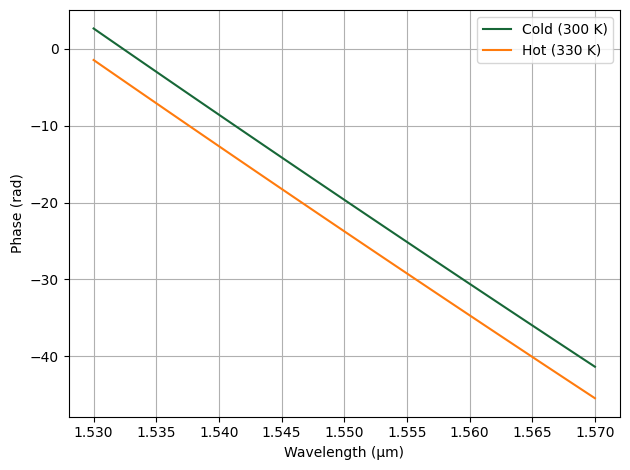
Thermo-Optic Tuning Verification This simulation compares the phase response of the heater at two different temperatures (300 K and 330 K) to verify the tuning efficiency. By extracting the phase of the \(S_{21}\) parameter, we can estimate the phase shift \(\Delta\phi\) per degree Kelvin, ensuring the shifter provides sufficient range for thermal compensation or signal modulation.
[25]:
# Compare phase response at two temperatures to estimate thermo-optic tuning
heater.update(temperature=330)
s_heater_hot = heater.s_matrix(freqs)
heater.update(temperature=293)
s_heater_cold = heater.s_matrix(freqs)
plt.plot(
wavelengths,
np.unwrap(np.angle(s_heater_cold[("P0@0", "P1@0")])),
label="Cold (293 K)",
)
plt.plot(
wavelengths,
np.unwrap(np.angle(s_heater_hot[("P0@0", "P1@0")])),
label="Hot (330 K)",
)
plt.xlabel("Wavelength (µm)")
plt.ylabel("Phase (rad)")
plt.legend()
plt.grid(True)
plt.tight_layout()
Progress: 100%
Progress: 100%
PN Phase Shifter
An MZM converts phase modulation into intensity modulation using two interferometer arms with phase shifters.
Design Tip: MZM Length vs. Extinction Ratio
Trade-off: Determining the optimal phase shifter length is a balance between signal quality and performance.
Too Short: You won’t achieve the required phase shift for your available voltage swing (\(V_{pp}\)), resulting in a poor Extinction Ratio (ER) (the “eye” won’t open fully).
Too Long: You get excellent ER, but you suffer from higher optical loss (absorption from dopants) and a larger footprint.
The Math: To find the “sweet spot” (minimum length for a target ER), we work backward from the desired contrast:
Target Phase Shift (:math:`phi`): For a push-pull MZM biased at quadrature, the ER is determined by the peak phase excursion \(\phi_{peak}\):
\[\sin(\phi_{peak}) = \frac{ER_{linear} - 1}{ER_{linear} + 1}\]Required :math:`V_{pi}`: We calculate how efficient the modulator needs to be to achieve that \(\phi_{peak}\) given your drive voltage \(V_{peak}\) (where \(V_{peak} = V_{pp}/2\)):
\[V_{\pi, required} = \frac{\pi \cdot V_{peak}}{\phi_{peak}}\]Required Length (:math:`L`): Finally, we use the modulator’s efficiency metric, \(V_{\pi}L_{push-pull}\) to find the physical length:
\[L = \frac{V_{\pi}L_{push-pull}}{V_{\pi, required}}\]
[26]:
def calculate_mzm_length(target_er_db, vpi_l, v_applied):
"""
Calculates the required length of an MZM for a given Extinction Ratio.
The Bias point is assumed to be 'quadrature' (max slope) for this calculation.
Parameters:
- target_er_db: Desired Extinction Ratio in dB
- vpi_l: Push-Pull Drive Modulation efficiency product (V*cm)
- v_applied: Peak-to-peak drive voltage (Volts)
Returns:
- length: Required length in um
"""
# Convert ER from dB to linear power ratio (Pmax / Pmin)
er_linear = 10 ** (target_er_db / 10.0)
# Determine the required modulation index (sin(phi))
sin_phi = (er_linear - 1) / (er_linear + 1)
# Calculate the phase shift (phi) in radians
phi_rad = np.asin(sin_phi)
# Determine V_peak (half of v_applied)
v_peak = v_applied / 2.0
# Calculate the required Half-Wave Voltage (V_pi)
if phi_rad == 0:
return 0.0, 0.0 # Avoid division by zero
v_pi_req = (np.pi * v_peak) / phi_rad
# Calculate required Length
length = vpi_l / v_pi_req * 1e4
return length
# --- Configuration ---
target_er = 3.0 # dB
vpi_L_v_cm = 1.0 # Push-pull drive (V.cm)
voltage_pp = 2.0 # Volts
# --- Calculation ---
ps_length = calculate_mzm_length(target_er, vpi_L_v_cm, voltage_pp)
Important Note: The \(V_{\pi}L\) value used above is for the push-pull system (combined efficiency). When defining the physics for a single phase-shifter arm (as we do in the component definition below), use twice this value (i.e., \(V_{\pi}L_{arm} = 2 \times V_{\pi}L_{push\text{-}pull}\)).
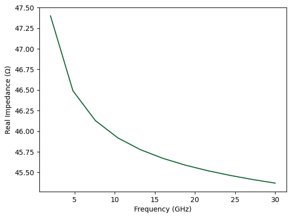
RF Design & Impedance Matching
High-speed traveling-wave modulators require careful RF engineering to ensure the electrical signal efficiently drives the optical phase shifter without debilitating reflections. We define an RF CPW port spec so electro-optic components can expose consistent electrical terminals.
Design Tip: A complete physical model of a PN modulator must account for the distributed RC loading of the active PN junction, which lowers the transmission line’s impedance and slows the RF phase velocity. Because modeling this active loading is highly complex, we will start by designing a baseline, unloaded 50 Ω Coplanar Waveguide (CPW).
The primary physical knobs for tuning the characteristic impedance of a CPW are the signal trace width and the gap spacing. Two quick rules of thumb:
Increasing the gap increases the impedance (less capacitive coupling to ground).
Increasing the signal width decreases the impedance (more surface area, higher capacitance).
[27]:
# Calculate RF mode, impedance, and group index for the active phase shifter CPW
freqs_rf = np.linspace(2, 30, 11) * 1e9
# Create a CPW port spec for RF electrodes
cpw_spec = pf.cpw_spec("M2_router", signal_width=35.0, gap=10.0, ground_width=75)
tech.add_port("CPW", cpw_spec)
mode_solver_rf, z0_rf = pf.port_modes(
cpw_spec, freqs_rf, mesh_refinement=30, impedance=True, group_index=True
)
plt.plot(freqs_rf / 1e9, z0_rf.isel(mode_index=0).real)
plt.xlabel("Frequency (GHz)")
plt.ylabel("Real Impedance (Ω)")
plt.show()
Uploading task 'Mode-ModeSolver…'Progress: 0% -
Starting task 'Mode-ModeSolver': https://tidy3d.simulation.cloud/workbench?taskId=mo-bf455d85-8d56-4151-b510-a658a8804d43
Downloading data from 'Mode-ModeSolver'…
Progress: 100%
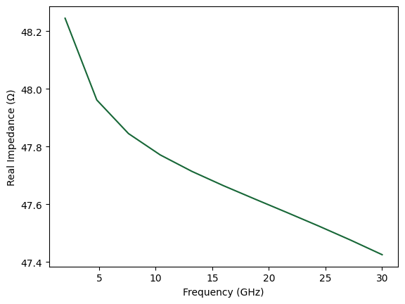
Design Tip: The RF probe pads themselves act as transmission lines. To ensure a clean signal transition from external RF probes (which are typically 50 Ω) onto the chip, we define a separate, wider CPW geometry for the Ground-Signal-Ground (GSG) pads and verify their impedance.
[28]:
# Define a CPW port spec for the GSG pads
pad_size = 100.0
pad_gap = 50.0 # (µm) gap distance from signal to ground
cpw_spec_pad = pf.cpw_spec(
"M2_router", signal_width=pad_size, gap=pad_gap, ground_width=pad_size
)
tech.add_port("CPW_Pad", cpw_spec_pad)
# Calculate impedance for the pad CPW geometry
mode_solver_pad, z0_pad = pf.port_modes(
cpw_spec_pad, freqs_rf, mesh_refinement=30, impedance=True, group_index=True
)
plt.plot(freqs_rf / 1e9, z0_pad.isel(mode_index=0).real)
plt.xlabel("Frequency (GHz)")
plt.ylabel("Real Impedance (Ω)")
plt.show()
Uploading task 'Mode-ModeSolver…'Progress: 0% -
Starting task 'Mode-ModeSolver': https://tidy3d.simulation.cloud/workbench?taskId=mo-66ede030-13c1-49fb-81ec-07ae2595df8f
Downloading data from 'Mode-ModeSolver'…
Progress: 100%
On-Chip Termination Material & Geometry
To prevent electrical back-reflections at the end of the traveling-wave electrode, the line must be terminated with an on-chip load matching the characteristic impedance (50 Ω). In a GSG (Ground-Signal-Ground) layout, this is efficiently achieved using two parallel 100 Ω resistors bridging the center signal trace to each ground trace.
Why use the Heater layer? Standard routing metals (like thick Aluminum or Copper) have high conductivity. If we tried to make a 100 Ω resistor out of standard routing metal, the trace would have to be microscopically narrow or incredibly long! Instead, we use the heater_metal layer (often TiN, TaN, or doped polysilicon). Because this layer is both physically thin (\(t\)) and has a lower conductivity (\(\sigma\)), it provides a high sheet resistance
(\(R_s = \frac{1}{\sigma t}\)), allowing us to hit 100 Ω with a compact, DRC-safe footprint.
[29]:
# Calculate the required physical width for the 100 ohm termination resistors
# We solve the resistance equation R = L / (sigma * W * t) for W.
# Here, L is the distance the current travels (pad_gap).
heater_thickness = tech.parametric_kwargs["heater_thickness"]
heater_conductivity = tech.parametric_kwargs["heater_metal"]["electrical"].conductivity
target_resistance = 100.0 # (Ohms) Two 100 Ohm resistors in parallel yield 50 Ohms
# Calculate required width (W = L / (R * sigma * t))
termination_width = pad_gap / (
target_resistance * heater_conductivity * heater_thickness
)
print(f"Required termination width for 100 Ohms: {termination_width:.2f} µm")
Required termination width for 100 Ohms: 12.50 µm
[30]:
@pf.parametric_component(name_prefix="PN Phase Shifter")
def pn_phase_shifter(
*,
length=3000, # phase shifter length (µm)
n_eff=n_eff_rib, # phase shifter effective index
n_group=n_group_rib, # phase shifter group index
ref_freq=freq0, # reference frequency for the effective and group indices
propagation_loss=5e-4, # phase shifter propagation loss (dB/µm)
v_piL=vpi_L_v_cm * 2 * 1e4, # Vpi.L (V.µm)
f3db=50e9, # 3 dB bandwidth
taper_length=10, # taper length (µm)
i_width=0.15, # intrinsic region width (µm)
p_width=0.5, # p-doping/n-doping width (µm)
pp_width=1.0, # p++ doping/n++ doping width (µm)
pad_size=pad_size, # RF pad size (µm)
pad_distance=300, # pad distance from shifter (µm)
pad_separation=pad_gap + pad_size, # pad separation (signal-ground) (µm)
termination_width=termination_width, # Termination width
):
"""
PN junction depletion-mode phase shifter for high-speed modulation.
Architecture:
- Rib waveguide (wider than strip for lower loss)
- PN junction laterally placed across waveguide
- Doping regions: p-contact, N, N++
- Traveling-wave electrode (CPW) for high bandwidth
- Dual-arm configuration for push-pull MZM
Physics:
- Free-carrier plasma dispersion effect
- Reverse-biased PN junction depletes carriers
- Phase shift: Δφ ∝ ΔV × L
Specs:
- Vπ·L: ~1-2 V·cm
- Loss: < 5 dB/cm
- Bandwidth: > 50 GHz
"""
rib_width = tech.ports["Rib_TE_1550_500"].width
# Create strip-to-rib tapers
taper = pf.parametric.transition(
port_spec1=port_spec, port_spec2=rib, length=taper_length
)
# Create straight rib section
straight = pf.parametric.straight(port_spec=rib, length=length, name="PS Arm")
# Add virtual electrical port for time domain simulation
elec_vir = pf.virtual_port_spec(classification="electrical")
straight.add_port(pf.Port((length / 2, 0), -90, spec=elec_vir))
# Create top arm phase modulator
mod_model = pf.AnalyticWaveguideModel(
n_eff=n_eff,
reference_frequency=ref_freq,
length=length,
propagation_loss=propagation_loss,
n_group=n_group,
v_piL=v_piL,
)
mod_model.time_stepper = pf.PhaseModTimeStepper(
length=length,
n_eff=n_eff,
n_group=n_group,
v_piL=v_piL,
propagation_loss=propagation_loss,
f_3dB=f3db,
)
straight.add_model(mod_model)
# Build component
c = pf.Component()
# Add first arm (top)
taper_in = c.add_reference(taper)
ps = c.add_reference(straight).connect("P0", taper_in["P1"])
taper_out = c.add_reference(taper).connect("P1", ps["P1"])
c.add_port([taper_in["P0"], taper_out["P0"]])
# Add doping regions to straight section
doping_regions = [
# (center, width, layer)
((i_width + p_width) / 2, p_width, "Si n"), # N-doping
((i_width + pp_width) / 2 + p_width, pp_width, "Si n++"), # N++ doping
(-(i_width + p_width) / 2, p_width, "Si p"), # P-doping
(-(i_width + pp_width) / 2 - p_width, pp_width, "Si p++"), # P++ doping
]
for y, width, layer in doping_regions:
straight.add(
layer,
pf.Rectangle(center=(length / 2, y), size=(length, width)),
# pf.Rectangle(corner2=(length, -y), size=(length, width)),
)
# Add CPW transmission line
w1, off1, _ = cpw_spec.path_profiles["gnd1"]
w0, off0, _ = cpw_spec.path_profiles["signal"]
offset = (w0 / 2 + off1 - w1 / 2) / 2
cpw = pf.parametric.straight(port_spec=cpw_spec, length=length + 2 * taper_length)
cpw_ref = pf.Reference(cpw, (0, -offset))
c.add(cpw_ref)
# Add second arm (bottom, for push-pull operation)
taper_in_2 = c.add_reference(pf.Reference(taper, origin=(0, -2 * offset)))
ps_2 = c.add_reference(pf.Reference(straight, origin=(0, -2 * offset))).connect(
"P0", taper_in_2["P1"]
)
taper_out_2 = c.add_reference(pf.Reference(taper, origin=(0, -2 * offset))).connect(
"P1", ps_2["P1"]
)
c.add_port([taper_in_2["P0"], taper_out_2["P0"], ps["E0"], ps_2["E0"]])
# Add RF terminals (pads)
c.add_terminal(
{
f"{name}:{side}": pf.Terminal(
"M2_router",
pf.Rectangle(center=(x, y - offset), size=(pad_size, pad_size)),
)
for x, side in [
(-pad_distance - pad_size / 2, "in"),
(length + 2 * taper_length + pad_distance + pad_size / 2, "out"),
]
for y, name in [
(-pad_separation, "gnd0"),
(0, "signal"),
(pad_separation, "gnd1"),
]
}
)
# Route from pads to CPW
for p, side in [("E0", "in"), ("E1", "out")]:
for name in ("gnd0", "signal", "gnd1"):
c.add(
pf.parametric.route_taper(
terminal1=c[f"{name}:{side}"], terminal2=cpw_ref[p].terminals(name)
)
)
# Add integrated termination at input
c.add(
"M1_heater",
pf.Path(c["gnd0:in"].center(), termination_width).segment(
c["gnd1:in"].center()
),
)
# Add circuit model
c.add_model(pf.CircuitModel(), "Circuit")
# Removing cpw models and ports to avoid warnings and errors because this component is not involved in circuit simulation
cpw.remove_model(list(cpw.models.keys())[0])
for port in list(cpw.ports.keys()):
cpw.remove_port(port)
return c
ps = pn_phase_shifter(length=ps_length)
viewer(ps)
[30]:

Mach-Zehnder Modulator (MZM) Test Assembly
To validate the calculated phase shifter length and the resulting extinction ratio, we assemble a test MZM using a virtual netlist. This configuration pairs the Y-junction splitters with the dual-arm PN phase shifter to simulate the full interference-based intensity modulation. This “virtual” assembly allows for rapid DC verification of the modulation depth before proceeding to the physical routing of the high-speed electrodes.
[31]:
# Define the Netlist for the Mach-Zehnder Modulator
netlist_mzm = {
"name": "MZM_PushPull_Virtual",
"instances": {
"SPLITTER": {"component": splitter, "origin": (-100, -15)},
"ARM": ps,
"COMBINER": {
"component": splitter,
"origin": (ps_length + 100, -15),
"rotation": 180,
},
},
# using "virtual_connections" allows logical linking without physical routing
"virtual_connections": [
# Splitter Output 2 -> Top Arm Input
(("SPLITTER", "P2"), ("ARM", "P0")),
# Splitter Output 1 -> Bottom Arm Input
(("SPLITTER", "P1"), ("ARM", "P2")),
# Top Arm Output -> Combiner Input 1
(("ARM", "P1"), ("COMBINER", "P1")),
# Bottom Arm Output -> Combiner Input 2
(("ARM", "P3"), ("COMBINER", "P2")),
],
"ports": [
("SPLITTER", "P0"), # Optical Input
("COMBINER", "P0"), # Optical Output
],
"models": [pf.CircuitModel()],
}
# Create component from netlist
mzm_device = pf.component_from_netlist(netlist_mzm)
viewer(mzm_device)
[31]:

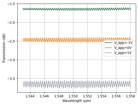
DC Verification: Extinction Ratio
Here we verify the design by simulating the static transmission at different voltage states.
We drive the MZM with the design voltage swing of 2 V:math:`_{pp}` (toggling between \(-1\) V and \(+1\) V relative to the bias).
Observation:
The plot below confirms that this voltage swing results in an Extinction Ratio (ER) of ~3 dB, successfully validating the length calculation performed in the previous step.
[32]:
v_bias = 7
voltages = [-1, 0, 1]
plt.figure()
for v_app in voltages:
# Update dictionary based on your previous cell structure
updates = {
(ps.name, 0, "PS Arm", 0): {"model_updates": {"voltage": v_bias + v_app}},
(ps.name, 0, "PS Arm", 1): {"model_updates": {"voltage": -v_app}},
}
# Compute S-matrix and extract Transmission (P0 -> P1)
S = mzm_device.s_matrix(freqs, model_kwargs={"updates": updates})
T_dB = 20 * np.log10(np.abs(S["P0@0", "P1@0"]))
plt.plot(wavelengths, T_dB, label=f"V_app={v_app}V")
plt.xlabel("Wavelength (µm)")
plt.ylabel("Transmission (dB)")
plt.legend()
plt.grid(True)
Uploading task 'P0@0…'
Uploading task 'P1@0…'
Uploading task 'Mode-Rib(90nmslab)TE1550nmw500nm…'
Uploading task 'Mode-Rib(90nmslab)TE1550nmw500nm…'
Starting task 'P0@0': https://tidy3d.simulation.cloud/workbench?taskId=fdve-d357772e-fb8c-41df-b655-710e5c46a92b
Downloading data from 'P0@0'…
Starting task 'P1@0': https://tidy3d.simulation.cloud/workbench?taskId=fdve-0aa753d5-eecf-4585-9ea7-f7310e35ecb5
Starting task 'Mode-Rib(90nmslab)TE1550nmw500nm': https://tidy3d.simulation.cloud/workbench?taskId=mo-bef9682c-4b28-41f2-96c7-f62036005a30
Starting task 'Mode-Rib(90nmslab)TE1550nmw500nm': https://tidy3d.simulation.cloud/workbench?taskId=mo-a9c7d360-d9fa-4a9e-96ab-42b384a4b1d0
Downloading data from 'P1@0'…
Downloading data from 'Mode-Rib(90nmslab)TE1550nmw500nm'…
Downloading data from 'Mode-Rib(90nmslab)TE1550nmw500nm'…
Progress: 100%
Progress: 100%
Progress: 100%
Waveguide Crossing
Waveguide crossings are essential for complex routing in high-density PICs, allowing signal paths to intersect with minimal interference.
Reference:
Ma et al., “Ultralow loss single layer submicron silicon waveguide crossing for SOI optical interconnect,” Opt Express, 2023 21 (24), 29374–29382, doi: 10.1364/OE.21.029374
Design Tip:
The Challenge: A direct waveguide intersection causes high loss and crosstalk because light diffracts (spreads out) as it crosses the unguided gap.
The Solution: We widen the waveguide before the crossing. A larger optical mode has a narrower divergence angle (\(\theta \propto \lambda/w\)), allowing it to “jump” the gap with minimal scattering.
Optimization: A linear taper is often too long. To minimize the footprint, we use an optimization algorithm (e.g., particle swarm optimization) to find a cubic-spline width profile. This algorithm determines the fastest possible rate of expansion that remains adiabatic—meaning the mode evolves smoothly without scattering energy into higher-order modes.
[33]:
from scipy.interpolate import make_interp_spline
default_widths = (
0.5,
0.6,
0.95,
1.32,
1.44,
1.46,
1.466,
1.52,
1.58,
1.62,
1.76,
2.15,
0.5,
)
@pf.parametric_component(name_prefix="Crossing")
def adiabatic_crossing(
*,
arm_length=4.5, # Length of crossing arms (µm)
widths=default_widths,
):
"""
Create a 4-arm adiabatic crossing with smooth cubic taper profiles.
Parameters:
arm_length (float): Length of the main arm (µm).
widths (Sequence[float]): Target waveguide widths (µm) along each arm.
Returns:
A crossing component.
"""
# Number of points used to discretize the cubic spline profile.
num_points = int(arm_length / pf.config.tolerance)
wg_width, _ = port_spec.path_profile_for("Si") # extract initial waveguide width
# Create cubic spline interpolation for widths
coords = np.linspace(0, arm_length, len(widths))
spline = make_interp_spline(coords, widths[::-1], k=3)
# Pre-compute widths and positions from the interpolation
coords = np.linspace(0, arm_length, num_points)
widths = spline(coords)
arm1 = pf.Path((0, 0), wg_width)
for x, w in zip(coords[1:], widths[1:]):
arm1.segment((x, 0), w)
arm2 = arm1.copy().rotate(90)
arm3 = arm1.copy().rotate(180)
arm4 = arm1.copy().rotate(270)
c = pf.Component()
c.add("Si", *pf.boolean([arm1, arm2], [arm3, arm4], "+"))
# Add ports
c.add_port(c.detect_ports([port_spec]))
assert len(c.ports) == 4, "Port detection failed: expected exactly 4 ports."
# Add Tidy3D simulation model with symmetry conditions
c.add_model(
pf.Tidy3DModel(
port_symmetries=[
("P1", "P0", "P3", "P2"), # symmetry about x-axis
("P2", "P3", "P0", "P1"), # symmetry about y-axis
("P3", "P2", "P1", "P0"), # inversion symmetry
],
),
"Tidy3D",
)
return c
crossing = adiabatic_crossing()
viewer(crossing)
[33]:

[34]:
# Compute the scattering matrix of the crossing over the frequency range
s_matrix_crossing = crossing.s_matrix(freqs)
# Plot the magnitude of the S-matrix to evaluate transmission and crosstalk
_ = pf.plot_s_matrix(s_matrix_crossing, input_ports=["P0"])
# Add the simulation results as a DataModel to avoid future FDTD simulations for different frequencies
# crossing.add_model(pf.DataModel(s_matrix_crossing))
Uploading task 'P0@0…'
Starting task 'P0@0': https://tidy3d.simulation.cloud/workbench?taskId=fdve-9263de75-621e-4709-aac8-de90f39843d9
Downloading data from 'P0@0'…
Progress: 100%
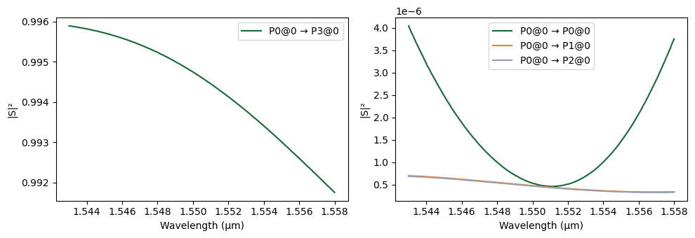
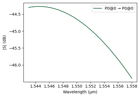
Optical Termination
This section defines a low-reflection waveguide termination used to suppress back-reflections at open waveguide ends.
Design Tip: To prevent destabilizing back-reflections (return loss), avoid abrupt waveguide cuts. Instead, use an adiabatic tapered termination.
By gradually narrowing the waveguide to a sharp tip (e.g., < 100 nm), the optical mode is forced to expand and radiate smoothly into the cladding (“mode deconfinement”). This “squeezes” the light out without creating a reflective facet, typically achieving reflections lower than -30 dB.
[35]:
# Load and visualize a low-reflection waveguide terminator PCell
termination = siepic.component("ebeam_terminator_te1550")
viewer(termination)
[35]:

Simulation shows very low return loss (< -45 dB).
[36]:
# Simulate and plot the terminator S-matrix
s_matrix_termination = termination.s_matrix(freqs)
_ = pf.plot_s_matrix(s_matrix_termination, y="dB", input_ports=["P0"])
# Add the simulation results as a DataModel to avoid future FDTD simulations for different frequencies
# termination.add_model(pf.DataModel(s_matrix_termination))
Uploading task 'P0@0…'
Starting task 'P0@0': https://tidy3d.simulation.cloud/workbench?taskId=fdve-795c0fb7-7823-4848-af71-789630be475f
Downloading data from 'P0@0'…
Progress: 100%
Bond Pads
Bond pads are the primary electrical interface between the photonic chip and the external environment. These large metal areas (typically 100 × 100 µm) are designed for wire bonding or flip-chip packaging, providing reliable electrical connections for DC biasing of heaters and high-speed RF signaling for modulators. The design ensures low contact resistance and sufficient surface area to accommodate standard packaging tolerances.
[37]:
bp = pf.Component("BondPad")
bp.add_terminal(pf.Terminal("M2_router", pf.Rectangle(size=(100, 100))), add_structure=True)
bp.add("M_Open", pf.Rectangle(size=(95, 95)))
viewer(bp)
[37]:
