
Waveguide Crossing Yield Analysis

Dense photonic circuits route hundreds of waveguide crossings, so a crossing must not only perform well at its nominal design, it must keep performing across the spread of silicon thickness and linewidth that a real fabrication process delivers. This example predicts the fabrication yield of an adiabatic waveguide crossing on the SiEPIC OpenEBL platform using the response-surface methodology of experimental design [1]:
Simulate the crossing with full 3D FDTD at a small set of process corners and samples.
Fit smooth polynomial response surfaces to the results, and check them against held-out simulations the fit has never seen.
Sample hundreds of virtual chips from a hierarchical wafer and lot variation model [2], evaluating each chip through the fitted surfaces in microseconds.
The full-wave cost is fixed by step 1 (fifteen simulations here), independent of how many chips step 3 samples. This is what makes statistical tolerance analysis affordable: the simulator explores the process space once, and the statistics are then free.
Reference
Box, George E. P., and Kenneth B. Wilson. “On the experimental attainment of optimum conditions.” Journal of the Royal Statistical Society: Series B 1951 13 (1), 1-45, doi: 10.1111/j.2517-6161.1951.tb00067.x.
Lu, Zeqin, et al. “Performance prediction for silicon photonics integrated circuits with layout-dependent correlated manufacturing variability.” Optics Express 2017 25 (9), 9712-9733, doi: 10.1364/OE.25.009712.
Ma, Yangjin, et al. “Ultralow loss single layer submicron silicon waveguide crossing for SOI optical interconnect.” Optics Express 2013 21 (24), 29374-29382, doi: 10.1364/OE.21.029374.
Technology and variation axes
The two dominant process variations on a silicon photonics platform are the device-layer thickness (a wafer-scale property of the SOI stock) and the waveguide linewidth, or critical dimension (CD), set by lithography and etch. Both are exposed as parameters of the SiEPIC OpenEBL technology: si_thickness sets the extruded silicon thickness, and si_mask_dilation moves every silicon mask edge outward by the given amount, so a dilation of \(d\) changes every width by \(2d\), exactly
like a litho or etch bias.
One setup detail matters here: the crossing uses 430 nm access waveguides, so a port specification for that width is created (by copying and adjusting the stock 500 nm TE port) and passed directly to the component.
[1]:
import numpy as np
import photonforge as pf
import siepic_forge as siepic
from scipy.interpolate import make_interp_spline
from matplotlib import pyplot as plt
from photonforge.live_viewer import LiveViewer

viewer = LiveViewer()

# SiEPIC OpenEBL technology at its nominal stack (220 nm silicon, no bias)
tech = siepic.ebeam()

# Port specification for the 430 nm access waveguides, made by copying and
# adjusting the stock 500 nm TE port. It is passed directly to the component,
# so it does not need to be registered in the technology.
wg_width = 0.43
port_spec = tech.ports["TE_1550_500"].copy()
port_spec.path_profiles = [(wg_width, 0.0, (1, 0))]
port_spec.description = "Strip TE 1550 nm, w=430 nm"

pf.config.default_technology = tech

# Analysis band: 11 wavelengths across the C band
wavelengths = np.linspace(1.53, 1.57, 11)
freqs = pf.C_0 / wavelengths
LiveViewer started at http://localhost:61644
Adiabatic crossing component
The crossing consists of four identical arms joined at the center. Each arm expands the 430 nm access waveguide through a cubic-spline width profile up to a wide multimode section at the junction, where the mode is strongly confined and expands slowly enough to cross the perpendicular arms with little scattering, the approach that established ultralow crossing loss on submicron SOI [3]. The spline knots (default_widths) were chosen so the expansion stays adiabatic over the C band.
The Tidy3DModel is attached inside the parametric function. The declared port_symmetries (both mirror planes and inversion) tell the model that a single FDTD excitation determines the response of symmetry-related inputs, which cuts the number of simulations per geometry.
[2]:
# Spline knot widths from the arm tip (port side) to the junction. The wide
# 2.15 um section sits next to the center; the final 0.5 um value is the
# width at the exact center, where the perpendicular arms overlap.
default_widths = (
    0.5, 0.6, 0.95, 1.32, 1.44, 1.46, 1.466,
    1.52, 1.58, 1.62, 1.76, 2.15, 0.5,
)


@pf.parametric_component(name_prefix="PLUS_CROSSING")
def adiabatic_plus_crossing(
    *,
    port_spec,
    arm_length=4.5,
    widths=default_widths,
    lead_length=1.0,
):
    if isinstance(port_spec, str):
        port_spec = pf.config.default_technology.ports[port_spec]

    wg_width, _ = port_spec.path_profile_for("Si")

    # Number of points used to discretize the cubic spline profile.
    num_points = int(arm_length / pf.config.tolerance)

    # Snap the port coordinate to the grid to avoid gaps/overlaps.
    xp = pf.snap_to_grid(arm_length + lead_length)

    # Cubic spline through the width knots (reversed so that 0 = center).
    coords = np.linspace(0, arm_length, len(widths))
    spline = make_interp_spline(coords, widths[::-1], k=3)

    # Pre-compute widths and positions from the interpolation.
    coords = np.linspace(arm_length, 0, num_points)
    w = spline(coords)

    # East arm: lead-in taper from the port, then the spline profile.
    arm_e = pf.Path((xp, 0), wg_width)
    arm_e.segment((coords[0], 0), width=(w[0], "smooth"))
    for x, wi in zip(coords[1:], w[1:]):
        arm_e.segment((x, 0), wi)

    # The other three arms are rotated copies of the east arm.
    arm_w = arm_e.copy().rotate(180)
    arm_n = arm_e.copy().rotate(90)
    arm_s = arm_e.copy().rotate(270)

    # Merge the four arms into a single silicon region.
    c = pf.Component()
    c.add("Si", *pf.boolean([arm_e, arm_w], [arm_n, arm_s], "+"))

    c.add_port(c.detect_ports([port_spec]))
    assert len(c.ports) == 4, "Port detection failed: expected exactly 4 ports."

    # Detected port order: P0 = West, P1 = South, P2 = North, P3 = East.
    c.add_model(
        pf.Tidy3DModel(
            grid_spec=12,
            port_symmetries=[
                ("P0", "P2", "P1", "P3"),  # symmetry about x-axis
                ("P3", "P1", "P2", "P0"),  # symmetry about y-axis
                ("P3", "P2", "P1", "P0"),  # inversion symmetry
            ],
        ),
        "Tidy3DModel",
    )
    return c


crossing = adiabatic_plus_crossing(port_spec=port_spec)
viewer(crossing)
[2]:

Nominal performance
A crossing is judged on three quantities: the through transmission (P0 to P3), the crosstalk scattered into the perpendicular arms (P0 to P1 and P2), and the back-reflection. We compute the full scattering matrix over the band and adopt the following acceptance criteria, evaluated at the worst wavelength: transmission above 98% and crosstalk below -30 dB.
[3]:
# Full S-matrix of the nominal crossing (one FDTD task after symmetries)
s_nominal = crossing.s_matrix(freqs)


def crossing_metrics(s):
    """Through power, worst crosstalk (dB) and reflection (dB) vs wavelength."""
    # Through path: west input to east output
    thru = np.abs(s[("P0@0", "P3@0")]) ** 2
    # Crosstalk: worst of the two perpendicular outputs
    xt = np.maximum(
        np.abs(s[("P0@0", "P1@0")]) ** 2,
        np.abs(s[("P0@0", "P2@0")]) ** 2,
    )
    # Back-reflection into the input port
    refl = np.abs(s[("P0@0", "P0@0")]) ** 2
    return thru, 10 * np.log10(xt), 10 * np.log10(refl)


t_nom, xt_nom, r_nom = crossing_metrics(s_nominal)

fig, (ax1, ax2) = plt.subplots(1, 2, figsize=(10, 3.6), tight_layout=True)
ax1.plot(wavelengths, 100 * t_nom, "o-")
ax1.axhline(98, color="tab:red", ls="--", label="98% criterion")
ax1.set_xlabel("wavelength (um)")
ax1.set_ylabel("transmission (%)")
ax1.legend()
ax1.grid(alpha=0.3)
ax2.plot(wavelengths, xt_nom, "o-", label="crosstalk")
ax2.plot(wavelengths, r_nom, "s--", label="reflection")
ax2.axhline(-30, color="tab:red", ls="--", label="-30 dB criterion")
ax2.set_xlabel("wavelength (um)")
ax2.set_ylabel("power (dB)")
ax2.legend()
ax2.grid(alpha=0.3)
plt.show()

print(f"worst-band transmission: {100 * t_nom.min():.2f}%")
print(f"worst-band crosstalk: {xt_nom.max():.1f} dB")
09:33:23 Eastern Daylight Time Loading simulation from local cache. View cached
                               task using web UI at
                               'https://tidy3d.simulation.cloud/workbench?taskId
                               =fdve-6f832e50-ee04-4241-8cf8-c55df1da8b04'.
09:33:24 Eastern Daylight Time Loading simulation from local cache. View cached
                               task using web UI at
                               'https://tidy3d.simulation.cloud/workbench?taskId
                               =fdve-51060b2d-005a-4857-b4dd-92d84ffc861a'.
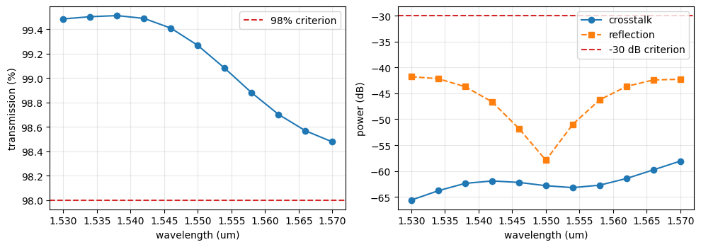
worst-band transmission: 98.48%
worst-band crosstalk: -58.0 dB
The nominal crossing transmits above 98.4% everywhere in the band, with the minimum at the red edge where the adiabatic expansion is slowly running out of margin. Crosstalk and reflection sit below -55 dB and -40 dB, far from their criterion. The 0.47 point transmission margin at the band edge is the quantity the process variation will eat into, so the yield question is a real one.
Process corner simulations
We now map how the metrics move across the process space. The monte_carlo.s_matrix function automates the whole batch: the two process deviations are declared as random variables of the technology with deliberately generous spreads (\(\sigma_t = 5\) nm for thickness and \(\sigma_w = 10\) nm for linewidth). Training the surface over a region wider than the production statistics used later keeps every sampled chip well inside the fitted box, so the analysis does not depend on the luck of a particular random draw. A single call evaluates
the four corner cases of the process box, whose edges are placed at 2.5 standard deviations by
corner_coverage, andten random samples inside the box (
random_samples).
Technology updates, component regeneration, parallel upload, and collection are all handled by the function. The four box corners alone cannot separate the two curvature terms of a quadratic surface, so the first eight random samples complete the training set, and the last two are set aside as hold-outs that never enter the fit. One FDTD input suffices per case because the four-fold symmetry of the crossing makes all inputs equivalent (the nominal run, which computed two independent inputs, confirms this equivalence to numerical precision).
[4]:
thickness_var = pf.monte_carlo.RandomVariable(
    "si_thickness", tech, value=0.220, stdev=0.005
)
# The mask dilation moves each silicon edge by half the linewidth change,
# so a 10 nm linewidth sigma is a 5 nm dilation sigma (values in um).
dilation_var = pf.monte_carlo.RandomVariable(
    "si_mask_dilation", tech, value=0.0, stdev=0.005
)

mc_variables, mc_results = pf.monte_carlo.s_matrix(
    crossing,
    freqs,
    thickness_var,
    dilation_var,
    corner_samples=-1,  # all 4 corners of the process box
    random_samples=10,  # random samples inside the box
    corner_coverage=0.9876,  # box edges at 2.5 standard deviations
    random_seed=0,
    model_kwargs={"inputs": ["P0"]},
)

# Each result is (*variable_values, s_matrix). The values follow the
# ordering of the returned variable list, which is not necessarily the
# order the variables were passed in, so look them up by variable name.
names = [v.name for v in mc_variables]
t_index = names.index("si_thickness")
w_index = names.index("si_mask_dilation")

doe, trans, cross = [], [], []
for *values, s in mc_results:
    dt = 1e3 * values[t_index] - 220.0
    dw = 2e3 * values[w_index]
    thru, xt, _ = crossing_metrics(s)
    doe.append((dt, dw))
    trans.append(thru)
    cross.append(xt)

# The 4 corners and the first 8 samples train the fit; the last 2 samples
# are reserved as hold-outs.
doe, trans, cross = np.array(doe), np.array(trans), np.array(cross)
doe_train, trans_train = doe[:-2], trans[:-2]
doe_holdout, trans_holdout = doe[-2:], trans[-2:]

print(" dt (nm)   dw (nm)   worst T (%)   worst XT (dB)")
for i, (dt, dw) in enumerate(doe):
    if i == len(doe_train):
        print(" ------------- hold-outs -------------")
    print(f"  {dt:+5.1f}    {dw:+5.1f}      {100 * trans[i].min():6.2f}        "
          f"{cross[i].max():6.1f}")
09:33:25 Eastern Daylight Time Loading simulation from local cache. View cached
                               task using web UI at
                               'https://tidy3d.simulation.cloud/workbench?taskId
                               =fdve-9533e102-c3ea-4326-9bc1-7ec1398eed4e'.
                               Loading simulation from local cache. View cached
                               task using web UI at
                               'https://tidy3d.simulation.cloud/workbench?taskId
                               =fdve-ffa85baa-0332-468d-90f6-5d9941df7614'.
09:33:27 Eastern Daylight Time Loading simulation from local cache. View cached
                               task using web UI at
                               'https://tidy3d.simulation.cloud/workbench?taskId
                               =fdve-e1ec1fe4-b211-4524-a229-50bdc346fc1f'.
09:33:28 Eastern Daylight Time Loading simulation from local cache. View cached
                               task using web UI at
                               'https://tidy3d.simulation.cloud/workbench?taskId
                               =fdve-337e6586-e6b6-417b-a95b-be67ca29cebe'.
09:33:29 Eastern Daylight Time Loading simulation from local cache. View cached
                               task using web UI at
                               'https://tidy3d.simulation.cloud/workbench?taskId
                               =fdve-c6aadd72-aac3-44ad-9486-e1d9553bb1ce'.
09:33:30 Eastern Daylight Time Loading simulation from local cache. View cached
                               task using web UI at
                               'https://tidy3d.simulation.cloud/workbench?taskId
                               =fdve-09918864-5b3d-41e9-abc6-f5f158eebb9b'.
                               Loading simulation from local cache. View cached
                               task using web UI at
                               'https://tidy3d.simulation.cloud/workbench?taskId
                               =fdve-88e63c39-aa0c-487d-a6f0-833626f92f1f'.
09:33:31 Eastern Daylight Time Loading simulation from local cache. View cached
                               task using web UI at
                               'https://tidy3d.simulation.cloud/workbench?taskId
                               =fdve-e93ced91-d184-42ce-9da9-e1b13ba6e6bf'.
09:33:32 Eastern Daylight Time Loading simulation from local cache. View cached
                               task using web UI at
                               'https://tidy3d.simulation.cloud/workbench?taskId
                               =fdve-924edafd-9283-4b84-8229-e15631ecd902'.
09:33:33 Eastern Daylight Time Loading simulation from local cache. View cached
                               task using web UI at
                               'https://tidy3d.simulation.cloud/workbench?taskId
                               =fdve-133889de-5384-4a2b-a237-030880c4817d'.
09:33:34 Eastern Daylight Time Loading simulation from local cache. View cached
                               task using web UI at
                               'https://tidy3d.simulation.cloud/workbench?taskId
                               =fdve-7cc3e42e-d853-4826-a45a-8a11517acaef'.
                               Loading simulation from local cache. View cached
                               task using web UI at
                               'https://tidy3d.simulation.cloud/workbench?taskId
                               =fdve-bd36a727-2842-4720-bbe7-0f1a2a23271c'.
09:33:35 Eastern Daylight Time Loading simulation from local cache. View cached
                               task using web UI at
                               'https://tidy3d.simulation.cloud/workbench?taskId
                               =fdve-9fb221ac-07d8-4365-9db9-7e2e9530bed9'.
09:33:36 Eastern Daylight Time Loading simulation from local cache. View cached
                               task using web UI at
                               'https://tidy3d.simulation.cloud/workbench?taskId
                               =fdve-471c4657-d8f1-4610-8023-af864d45951d'.
 dt (nm)   dw (nm)   worst T (%)   worst XT (dB)
  -12.5    -25.0       95.72         -48.6
  +12.5    -25.0       96.79         -50.5
  -12.5    +25.0       99.02         -56.4
  +12.5    +25.0       98.37         -47.2
   +0.9    +12.0       99.18         -52.8
   -0.7     +1.0       98.54         -58.2
   -1.4    -19.2       96.98         -49.5
   -2.9    +16.3       99.07         -52.6
   +4.1     +3.4       98.93         -57.7
  -14.4     -8.6       96.96         -53.5
  +11.1     -3.9       98.75         -60.5
   +1.9     -0.8       98.54         -59.2
 ------------- hold-outs -------------
   +5.5     -6.6       98.25         -58.8
   -4.7     +5.6       98.80         -58.5
The worst-band transmission is lowest at the thin and narrow corner and highest at the thick and wide one: more silicon always helps this crossing, and the 98% criterion boundary lies inside the process box. Crosstalk stays below -47 dB at every sampled point. Since that is more than 17 dB inside the -30 dB criterion, crosstalk cannot drive yield and we treat it as bounded by its worst sampled value instead of fitting a surface to it (at these levels the FDTD result is dominated by its numerical noise floor, so a fitted surface would model noise, not physics).
Transmission response surface
The transmission at each wavelength is fitted as a quadratic in the two deviations, anchored exactly at the nominal:
The twelve training cases determine the five coefficients per wavelength by least squares. The purpose of the plot below is to test the accuracy of the fitted surface: the two hold-out samples were never used in the fit, so comparing their FDTD spectra (markers) with the surface’s predictions at the same deviations (lines) measures the model’s true prediction error.
[5]:
def q_basis(dt, dw):
    """Quadratic basis terms (dt, dw, dt^2, dw^2, dt*dw) for the fit."""
    dt, dw = np.asarray(dt, float), np.asarray(dw, float)
    return np.stack([dt, dw, dt**2, dw**2, dt * dw], axis=-1)


# Fit the deviation from the nominal spectrum: 12 training cases determine
# the 5 coefficients per wavelength by least squares.
a_train = q_basis(doe_train[:, 0], doe_train[:, 1])
y_train = trans_train - t_nom
t_coef = np.linalg.lstsq(a_train, y_train, rcond=None)[0]


def t_model(dt, dw):
    """Predicted transmission spectrum at deviation (dt, dw) in nm."""
    return t_nom + q_basis(dt, dw) @ t_coef


# The two hold-outs measure the model's true prediction error.
holdout_err = max(
    np.max(np.abs(t_model(dt, dw) - t))
    for (dt, dw), t in zip(doe_holdout, trans_holdout)
)

fig, ax = plt.subplots(figsize=(7.5, 4.2), tight_layout=True)
for (dt, dw), t, color in zip(doe_holdout, trans_holdout, ("tab:blue", "tab:orange")):
    # Response-surface prediction at the held-out deviation
    ax.plot(wavelengths, 100 * t_model(dt, dw), color=color, lw=2.5,
            label=f"fit at ({dt:+.1f}, {dw:+.1f}) nm")
    # FDTD simulation at the same deviation, never used in the fit
    ax.plot(wavelengths, 100 * t, "o", color=color,
            ms=7, ls="none")
ax.plot([], [], "ko", ms=7, label="FDTD (not used in the fit)")
ax.set_xlabel("wavelength (um)")
ax.set_ylabel("transmission (%)")
ax.legend()
ax.grid(alpha=0.3)
plt.show()

print(f"largest hold-out error: {100 * holdout_err:.2f} transmission points")
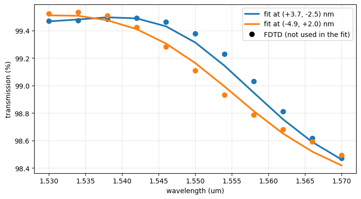
largest hold-out error: 0.16 transmission points
The held-out simulations land on the predicted curves to a fraction of a transmission point, an order of magnitude tighter than the margins that decide pass or fail, so the surface can stand in for the simulator across the whole box.
Wafer and lot variation analysis
Real variation is hierarchical: silicon thickness and CD differ from lot to lot, from wafer to wafer within a lot, and across each wafer [2]. We use a compact model of that hierarchy with production budgets of \(\sigma_t \approx 4\) nm and \(\sigma_w \approx 3.3\) nm, split between a lot offset, a wafer offset, a systematic across-wafer profile (radial bow for thickness, a linear tilt for CD), and a per-chip random term. The level contributions are independent, so they add in quadrature: for thickness, \(\sqrt{3.49^2 + 1.75^2 + 0.6^2 + 0.87^2} \approx 4\) nm. Both budgets sit well inside the wider box the response surface was trained on. Every chip is then a \((\Delta t, \Delta w)\) pair evaluated through the fitted surface, and its worst-band transmission decides pass or fail.
[6]:
rng = np.random.default_rng(1)
n_lots, n_wafers, n_chips = 4, 20, 50
wafer_radius = 100.0  # mm

# Fixed chip sample plan (same die positions measured on every wafer),
# drawn uniformly inside 90% of the wafer radius. The set is sorted so
# the plan does not depend on the interpreter's set ordering.
samples = set()
while len(samples) < n_chips:
    x, y = np.round(rng.uniform(-0.9, 0.9, 2), decimals=2)
    if x**2 + y**2 < 0.81:
        samples.add((float(x) * wafer_radius, float(y) * wafer_radius))
site_x, site_y = np.array(sorted(samples)).T
r2 = (site_x**2 + site_y**2) / wafer_radius**2  # normalized radius squared

records = []
for lot in range(n_lots):
    # Lot offsets: every wafer in the lot shares them
    lot_t = rng.normal(0, 3.49)
    lot_w = rng.normal(0, 0.72)
    for wafer in range(n_wafers):
        # Wafer offsets on top of the lot offsets
        wafer_t = lot_t + rng.normal(0, 1.75)
        wafer_w = lot_w + rng.normal(0, 1.44)
        # Chip values: systematic across-wafer profile + per-chip random term
        chip_t = wafer_t - 3.0 * (r2 - 0.5) + rng.normal(0, 0.87, n_chips)
        chip_w = wafer_w + 1.3 * site_x / wafer_radius + rng.normal(0, 2.88, n_chips)
        if lot == 0 and wafer == 0:
            # Keep the first wafer for the wafer-map figure below
            example_wafer = (wafer_t, wafer_w, chip_t.copy(), chip_w.copy())
        for dt, dw in zip(chip_t, chip_w):
            # Evaluate inside the trained box (rare outliers are clamped)
            dtc, dwc = np.clip(dt, -12.5, 12.5), np.clip(dw, -25.0, 25.0)
            records.append((lot, wafer, dt, dw, t_model(dtc, dwc).min()))

lot_idx = np.array([r[0] for r in records])
wafer_idx = np.array([r[1] for r in records])
chip_dt = np.array([r[2] for r in records])
chip_dw = np.array([r[3] for r in records])
t_worst = np.array([r[4] for r in records])

n = len(records)
passed = t_worst > 0.98
yield_est = passed.mean()

# Wilson 95% confidence interval on the yield estimate
z = 1.96
center = (yield_est + z**2 / (2 * n)) / (1 + z**2 / n)
half = z * np.sqrt(yield_est * (1 - yield_est) / n + z**2 / (4 * n**2)) / (1 + z**2 / n)

print(f"chips: {n}")
print(f"yield (worst-band T > 98%): {100 * yield_est:.1f}%  "
      f"(95% CI {100 * (center - half):.1f}-{100 * (center + half):.1f}%)")
chips: 4000
yield (worst-band T > 98%): 90.5%  (95% CI 89.5-91.3%)
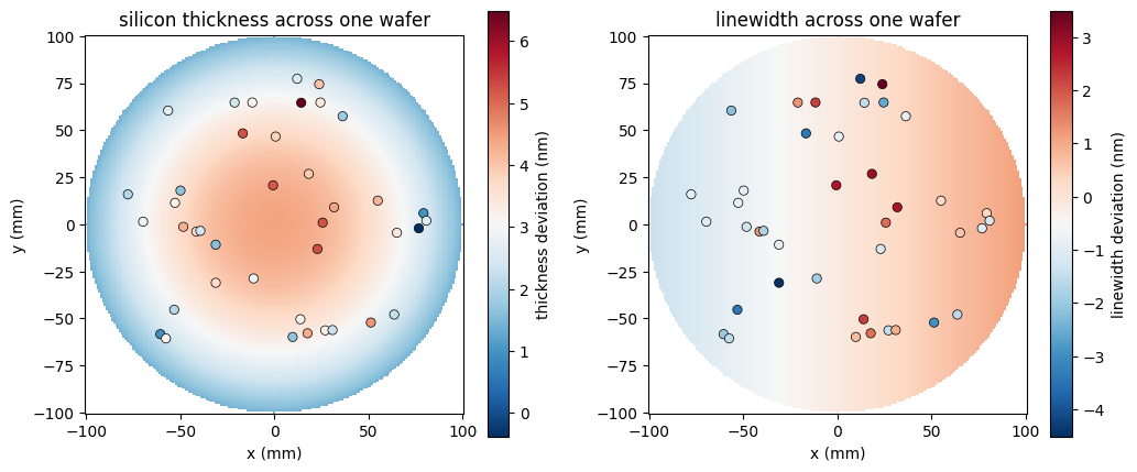
The hierarchy is easiest to see on a single wafer. The maps below show the thickness and linewidth deviations across the first sampled wafer: the smooth background combines the lot and wafer offsets with the systematic across-wafer profiles (a radial bow for thickness and a linear tilt for linewidth), and the dots are the sampled chip sites, which add the per-chip random term on top of the smooth map.
[7]:
wafer_t0, wafer_w0, chips_t0, chips_w0 = example_wafer

# Systematic wafer-scale profiles evaluated on a grid covering the wafer
axis_mm = np.linspace(-wafer_radius, wafer_radius, 201)
gx, gy = np.meshgrid(axis_mm, axis_mm)
inside = gx**2 + gy**2 <= wafer_radius**2
rr2 = (gx**2 + gy**2) / wafer_radius**2
map_t = np.where(inside, wafer_t0 - 3.0 * (rr2 - 0.5), np.nan)
map_w = np.where(inside, wafer_w0 + 1.3 * gx / wafer_radius, np.nan)

fig, axes = plt.subplots(1, 2, figsize=(10.5, 4.4), tight_layout=True)
for ax, field, chips, label in (
    (axes[0], map_t, chips_t0, "thickness deviation (nm)"),
    (axes[1], map_w, chips_w0, "linewidth deviation (nm)"),
):
    # Shared color scale between the smooth map and the chip sites
    vmin = min(np.nanmin(field), chips.min())
    vmax = max(np.nanmax(field), chips.max())
    mesh = ax.pcolormesh(gx, gy, field, cmap="RdBu_r", vmin=vmin, vmax=vmax,
                         shading="auto")
    ax.scatter(site_x, site_y, c=chips, cmap="RdBu_r", vmin=vmin, vmax=vmax,
               s=36, edgecolors="black", linewidths=0.5)
    plt.colorbar(mesh, ax=ax, label=label)
    ax.set_aspect("equal")
    ax.set_xlabel("x (mm)")
    ax.set_ylabel("y (mm)")
axes[0].set_title("silicon thickness across one wafer")
axes[1].set_title("linewidth across one wafer")
plt.show()
[8]:
fig, (ax1, ax2) = plt.subplots(2, 1, figsize=(10.5, 7), tight_layout=True)

# One box per wafer, colored by lot: exposes which hierarchy level moves
data, positions, box_colors = [], [], []
cmap = plt.get_cmap("tab10")
for lot in range(n_lots):
    for wafer in range(n_wafers):
        sel = (lot_idx == lot) & (wafer_idx == wafer)
        data.append(100 * t_worst[sel])
        positions.append(lot * (n_wafers + 2) + wafer)
        box_colors.append(cmap(lot))
boxes = ax1.boxplot(data, positions=positions, widths=0.7, patch_artist=True)
for patch, color in zip(boxes["boxes"], box_colors):
    patch.set_facecolor(color)
ax1.axhline(98, color="tab:red", ls="--")
ax1.set_xticks([lot * (n_wafers + 2) + n_wafers / 2 for lot in range(n_lots)])
ax1.set_xticklabels([f"lot {lot + 1}" for lot in range(n_lots)])
ax1.set_ylabel("worst-band transmission (%)")
ax1.set_title("per-wafer distributions, grouped by lot")

# Population histogram against the acceptance criterion
ax2.hist(100 * t_worst, bins=40)
ax2.axvline(98, color="tab:red", ls="--", label="98% criterion")
ax2.set_xlabel("worst-band transmission (%)")
ax2.set_ylabel("chips")
ax2.set_title(f"{n} chips, yield {100 * yield_est:.1f}%")
ax2.legend()
plt.show()
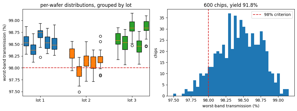
The box plots separate the hierarchy levels: the lot offsets move whole groups together (the lot that draws the thinnest silicon sits lowest and straddles the criterion), while the per-chip linewidth term sets the width of every box, so failures come from the low tail of each wafer, concentrated in the unluckiest lot. For a fab this is actionable: screening incoming wafers on device-layer thickness removes the worst lots, and tightening local CD control narrows every box.
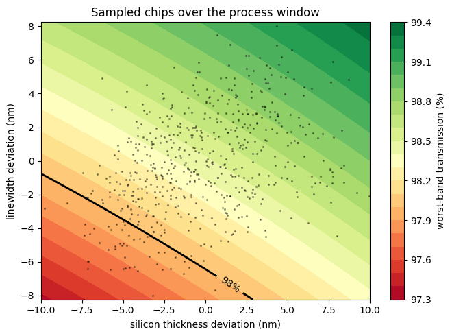
The same data can be viewed directly in the process plane. The map below shows the worst-band transmission predicted by the response surface over the whole deviation box, the 98% criterion boundary, and every sampled chip.
[9]:
# Evaluate the response surface on a grid covering the process box
dt_grid = np.linspace(-12.5, 12.5, 121)
dw_grid = np.linspace(-12.5, 12.5, 121)
dt_mesh, dw_mesh = np.meshgrid(dt_grid, dw_grid, indexing="ij")
# Worst-band value at every grid point: minimum of the spectrum
t_map = t_model(dt_mesh.ravel()[:, None], dw_mesh.ravel()[:, None])
t_map = t_map.reshape(dt_mesh.shape + (-1,)).min(axis=-1)

fig, ax = plt.subplots(figsize=(6.8, 5), tight_layout=True)
contours = ax.contourf(dt_mesh, dw_mesh, 100 * t_map, 21, cmap="RdYlGn")
plt.colorbar(contours, ax=ax, label="worst-band transmission (%)")
# The acceptance boundary in the process plane
boundary = ax.contour(dt_mesh, dw_mesh, 100 * t_map, levels=[98.0],
                      colors="k", linewidths=2)
ax.clabel(boundary, fmt="98%%")
# Every sampled chip at its process deviation
ax.plot(chip_dt, chip_dw, "k.", ms=2.5, alpha=0.35)
ax.set_xlim(-12.5, 12.5)
ax.set_ylim(-12.5, 12.5)
ax.set_xlabel("silicon thickness deviation (nm)")
ax.set_ylabel("linewidth deviation (nm)")
ax.set_title("Sampled chips over the process window")
plt.show()
Reading the surface as a design tool
The fitted coefficients also quantify how to buy margin. At the worst wavelength the surface slopes are about +0.05 transmission points per nm of silicon thickness and +0.07 points per nm of linewidth: this crossing always improves with more silicon. Thickness is not a designer’s knob, but linewidth is, since the drawn layout can be biased. Widening the drawn profile by 5 to 10 nm would roughly double the worst-band margin at zero cost, moving the criterion boundary mostly out of the process box. Re-centering the transmission peak (currently near 1.538 um) onto the band center by retuning the spline profile would have a similar effect. Both changes can be evaluated through the same corner-plus-surface workflow before committing a new layout.
The method shown here generalizes to any component whose response varies smoothly across the process box: simulate a designed set of corners once, prove the surface on held-out corners, then sample the process for free. Resonant devices need one adaptation, fitting physical parameters such as coupling and effective index instead of raw spectra, but the corner budget and the statistical machinery stay the same.