Inverse Design of a Fabrication-Robust Bent Directional Coupler
A directional coupler splits light through evanescent coupling between two adjacent waveguides. By curving both arms through the coupling region - creating a bent coupler - the splitting ratio becomes significantly less sensitive to wavelength variations [1].

While the original paper demonstrates this concept, it does not provide the exact geometric details of the bent coupler profile. Therefore, we initialize our device with a qualitatively similar shape. As a result, the performance of this starting design is far from optimized.
To fix this, we employ gradient-based inverse design on a standard 220 nm silicon-on-insulator (SOI) strip platform (targeted for the O-band, utilizing 380 nm wide waveguides and a 100 nm coupling gap). Our goal is to take this baseline and achieve a precise 50:50 splitting ratio that remains highly robust against fabrication dilation (a uniform over- or under-etching effect that alters waveguide widths and coupling gaps).
Geometry The layout of the two arms is defined compactly to ensure smooth, low-loss routing:
Bottom Arm: Features a fixed, smooth trajectory whose tightest bend radius is capped at
R_minto prevent excessive bending loss.Top Arm: Positioned at a center-to-center distance of
s(x)above the bottom arm, defined astop_y(x) = bottom_y(x) + s(x). By symmetry, the separation profiles(x)is an even function and is only parametrized on the left half of the device.
Design Variables The separation profile s(x) is a smooth, analytic curve governed by three shape “knobs”:
x_flat: The half-width of the 100 nm tight-coupling region.x_rise: The distance over which the gap opens.gamma: The skew of the opening curve.
These are optimized alongside two bottom-arm parameters:
R_bent: The radius of the coupling arc.theta: The angle of the coupling arc.
This yields a total of five scalar design variables. The absolute positions of the four ports are held strictly fixed, which is a requirement for the FDTD adjoint method.
Workflow
Initialize: Build the starting device using an
s(x)profile chosen to mimic the original paper.Baseline Simulation: Simulate the initial unoptimized device.
Adjoint Optimization: Iteratively improve the design using the adjoint gradient.
Verification: Simulate the finalized device and evaluate its robustness to fabrication dilation corners.
💡 Note on Computational Cost > Each optimization iteration requires 4 FDTD simulations. Since each simulation costs approximately 2.3 FlexCredits (FC), the total computational cost is ~10 FC per optimization iteration.
Reference
El-Saeed, Ahmed H., et al. “Low-loss silicon directional coupler with arbitrary coupling ratios for broadband wavelength operation based on bent waveguides.” Journal of Lightwave Technology 2024 42 (13), 6011-6018, doi: 10.1109/JLT.2024.3407339.
[1]:
import numpy as np
import matplotlib.pyplot as plt
from scipy.optimize import least_squares          # solves the bottom-arm lengths (keeps ports fixed)
import autograd.numpy as anp                        # autograd-traced numpy for the objective
from autograd import value_and_grad                 # cost and its adjoint gradient together
import photonforge as pf
import tidy3d as td
from photonforge.models.tidy3d import Tidy3DAutogradConfig
from IPython.display import clear_output

pf.config.default_technology = pf.basic_technology()
Parameters
The paper does not give an accurate description of the device, so we use a smooth separation profile s(x) with a few shape knobs, with initial values chosen so the simulated response mimics the bent directional coupler in the paper. Everything the notebook needs is defined here; it does not depend on any external layout or other notebook.
The device length (x_half), the bottom-arm climb (climb) and the port separation (s_port) are held fixed so the four ports never move as the design variables change.
[2]:
# --- fixed platform / geometry constants ---
width = 0.38          # waveguide width (um)
gap = 0.10            # coupling gap at the center (um) -> s(center) = width + gap, held at 100 nm
r_min = 5.0           # minimum bend radius of the bottom arm (curvature cap, low loss)
kcap = 1.0 / r_min    # corresponding maximum curvature

# --- fixed frame so the four ports stay put (required by the adjoint gradient) ---
x_half = 13.83        # device half-length: ports sit at x = +-x_half
climb = 2.60          # depth of the bottom port below the central apex
s_port = 4.31         # center-to-center separation at the ports (top port held here)

# --- initial design (chosen so the response mimics the paper) ---
r_bent0 = 25.0        # initial coupling-arc radius (um)
theta0 = 8.5          # initial coupling-arc angle (deg)
# s(x) shape knobs: a flat 100 nm coupling region of half-width x_flat that opens to s_port over x_rise,
# with opening skew gamma. (x_flat + x_rise <= x_half keeps the profile saturated at the port.)
x_flat0 = 4.35        # half-width of the flat coupling region (um)
x_rise0 = 8.64        # opening length (um)
gamma0 = 1.53         # opening skew

pf.config.default_technology = pf.basic_technology(strip_width=width)
Geometry builders
The bottom arm is built from its signed-curvature profile: starting horizontal at the port it dips to the curvature cap 1/R_min, rises monotonically to the coupling curvature 1/R_bent, and holds it over the central arc (so the access bends are never tighter than R_min and the coupling region is a real arc). Three segment lengths are solved so that, for any R_bent/theta, the apex is horizontal, the half-length equals x_half, and the climb is fixed – this is what keeps the
ports stationary.
The top arm is then placed directly above the bottom at the separation s(x). s(x) is a smooth, even profile: it sits flat at width + gap (the 100 nm coupling gap) over a central region of half-width x_flat, then opens to the port separation s_port over a length x_rise, with the opening shaped by gamma. Because s(x) is flat (zero first and second derivative) at both the center and the ports, the top arm inherits the bottom’s curvature exactly over the coupling arc
and stays horizontal at the ports, so all the geometry constraints are met for any value of the knobs.
[3]:
def smoothstep(t):
    """C1 ramp from 0 to 1 used to join curvature segments smoothly."""
    t = np.clip(t, 0.0, 1.0)
    return t**2 * (3 - 2 * t)


def smootherstep(t):
    """C2 ramp from 0 to 1 (zero first and second derivative at both ends) for the separation profile."""
    t = np.clip(t, 0.0, 1.0)
    return t**3 * (10 + t * (6 * t - 15))


def _integrate_curvature(s, k):
    """Integrate a signed-curvature profile k(s) into a centerline (heading, then x/y)."""
    ds = np.gradient(s)
    heading = np.cumsum(-k * ds)                     # +1/R_bent gives a concave-down crest
    x = np.cumsum(np.cos(heading) * ds)
    y = np.cumsum(np.sin(heading) * ds)
    return heading, np.column_stack([x, y])


def _curvature_profile(knots, n=240):
    """Concatenate segments, each ramping (via smoothstep) from one curvature to the next."""
    s_all, k_all, s_offset = [], [], 0.0
    for i, (length, k_start, k_end) in enumerate(knots):
        length = max(length, 1e-3)
        ss = np.linspace(0, length, n)
        kk = k_start + (k_end - k_start) * smoothstep(ss / length)
        s_all.append(ss if i == 0 else s_offset + ss[1:])
        k_all.append(kk if i == 0 else kk[1:])
        s_offset += length
    return np.concatenate(s_all), np.concatenate(k_all)


def bottom_arm(r_bent, theta_deg):
    """Build the full (mirrored) bottom centerline, apex at the origin, ports fixed at x = +-x_half."""
    kc = 1.0 / r_bent
    s_arc = r_bent * np.deg2rad(theta_deg) / 2       # arclength of the half coupling arc

    def half(lengths):
        # port -> dip (-1/R_min) -> rise to +1/R_bent -> hold over the coupling arc
        l1, l2, l3 = lengths
        s, k = _curvature_profile([(l1, 0.0, -kcap),       # dip up away from the port
                                   (l2, -kcap, 0.6 * kc),  # quick rise back through zero
                                   (l3, 0.6 * kc, kc),     # slow rise to the coupling curvature
                                   (s_arc, kc, kc)])        # constant-curvature coupling arc
        return _integrate_curvature(s, k)

    # solve the three lengths so the apex is horizontal, the half-span is x_half, and the climb is fixed
    sol = least_squares(
        lambda u: [half(u)[0][-1],                 # apex heading = 0
                   half(u)[1][-1, 0] - x_half,      # apex x = x_half (port at -x_half after centering)
                   half(u)[1][-1, 1] - climb],      # apex is 'climb' above the port
        x0=[3.6, 1.5, 10.0], bounds=([0.3, 0.3, 0.3], [40, 40, 40]), xtol=1e-11, ftol=1e-11)

    _, pts = half(sol.x)
    pts = pts - pts[-1]                              # shift so the apex is at the origin
    left = pts                                       # this half runs apex -> right port; mirror for the left
    right = np.column_stack([-pts[::-1, 0], pts[::-1, 1]])[1:]
    return np.vstack([left, right])


def separation(x, x_flat, x_rise, gamma):
    """Smooth, even separation profile s(x): flat at width+gap (100 nm gap) for |x| < x_flat, opening to
    s_port over x_rise with skew gamma. smootherstep is flat at both ends for any gamma, so s'(0)=s''(0)=0
    (apex stays horizontal, top arc matches the bottom) and s'=s''=0 at the port (top port horizontal)."""
    t = np.clip((np.abs(x) - x_flat) / x_rise, 0.0, 1.0)
    # raise only strictly-positive t to the gamma power (floor the base so 0**gamma never evaluates
    # log(0)); the flat region is restored to exactly 0, so s(center) = width + gap is unchanged
    warp = np.where(t > 0.0, np.clip(t, 1e-12, 1.0) ** gamma, 0.0)
    return (width + gap) + (s_port - (width + gap)) * smootherstep(warp)


def place_top(bc, x_flat, x_rise, gamma):
    """Top centerline = bottom + s(x), with s(x) the smooth few-knob separation profile."""
    bc = bc[np.argsort(bc[:, 0])]
    s_x = separation(bc[:, 0], x_flat, x_rise, gamma)
    return bc, np.column_stack([bc[:, 0], bc[:, 1] + s_x])
Parametric component (traced for autograd)
bent_dc assembles the two waveguides, the cladding and the four ports, and attaches a Tidy3D model. R_bent, theta_deg, x_flat, x_rise and gamma are the traced design variables: PhotonForge runs the factory body on plain values and obtains the gradient from the resulting geometry via the FDTD adjoint. Because the five knobs each reshape the whole device smoothly, the geometry finite-difference step is well behaved; autograd_config sets a modest relative step per
knob. dilation biases every edge to emulate fabrication over/under-etch (a sweep parameter, not traced).
[4]:
@pf.parametric_component
def bent_dc(*, r_bent=r_bent0, theta_deg=theta0, x_flat=x_flat0, x_rise=x_rise0, gamma=gamma0,
            technology=None):
    tech = technology or pf.config.default_technology
    strip = tech.ports["Strip"]
    clad_margin = (strip.path_profile_for("WG_CLAD")[0] - width) / 2

    # build both centerlines
    bc = bottom_arm(r_bent, theta_deg)
    bc, tc = place_top(bc, x_flat, x_rise, gamma)

    comp = pf.Component("bent_dc", technology=tech)
    for curve in (bc, tc):
        curve = curve[np.argsort(curve[:, 0])]
        path = pf.Path((float(curve[0, 0]), float(curve[0, 1])), width)
        path.segment(curve[1:].tolist())
        comp.add("WG_CORE", path)

    # cladding envelope around the cores
    comp.add("WG_CLAD", pf.envelope(comp.get_structures("WG_CORE"), clad_margin,
                                    trim_x_min=True, trim_x_max=True))

    # detect the ports at the waveguide terminals
    comp.add_port(comp.detect_ports([strip]))

    # 2% FD step for shape knobs; 1% for arc params (larger geometry lever -> smaller step better conditioned).
    # A step is accepted only if the perturbed-mode field-overlap with the nominal >= consistency_similarity_threshold
    # and the magnitude does not shift by more than consistency_magnitude_tolerance; otherwise retried up to max_diff_attempts.
    autograd_config = Tidy3DAutogradConfig(
        relative_diff_step={"x_flat": 0.02, "x_rise": 0.02, "gamma": 0.005,
                            "r_bent": 0.01, "theta_deg": 0.01},
        absolute_diff_step=1e-3,              # 1 nm floor so the step never collapses near zero
        consistency_similarity_threshold=0.8, # mode overlap with nominal must be >= 0.8
        consistency_magnitude_tolerance=0.3,  # field magnitude must not shift > 30%
        max_diff_attempts=8)                  # retry budget per parameter before giving up
    comp.add_model(pf.Tidy3DModel(autograd_config=autograd_config))
    return comp


# build the initial device and show its layout
dev0 = bent_dc(r_bent=r_bent0, theta_deg=theta0, x_flat=x_flat0, x_rise=x_rise0, gamma=gamma0)
print("ports:", {n: (round(p.center[0], 2), round(p.center[1], 2)) for n, p in dev0.ports.items()})
dev0
ports: {'P0': (np.float64(-13.82), np.float64(-2.6)), 'P1': (np.float64(-13.82), np.float64(1.71)), 'P2': (np.float64(13.82), np.float64(-2.6)), 'P3': (np.float64(13.82), np.float64(1.71))}
[4]:

Response of the initial device
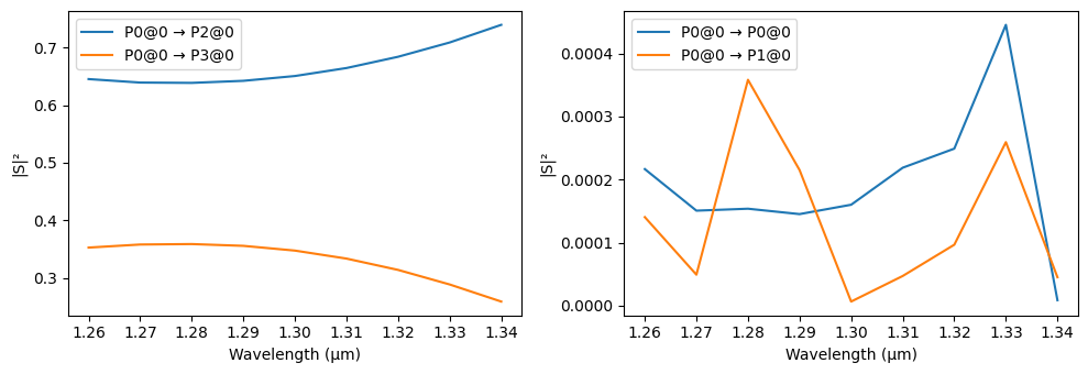
Sweep the O-band and look at the full scattering matrix of the starting design. With the input at P0, the through port is P2 (same arm) and the cross port is P3 (the other arm).
[5]:
lams = np.linspace(1.26, 1.34, 9)                 # O-band sweep (um)
s_0 = dev0.s_matrix(pf.C_0 / lams, model_kwargs={"inputs": ["P0"]}, show_progress=True)
_ = pf.plot_s_matrix(s_0)
Uploading task 'P0@0…'
Starting task 'P0@0': https://tidy3d.simulation.cloud/workbench?taskId=fdve-4465aa4a-ac9d-4880-9cab-145da70cbd0c
Downloading data from 'P0@0'…
Progress: 100%
Objective
We want a 50:50 split that is insensitive to dilation, so we minimize the squared deviation of the cross fraction from 0.5 at the center wavelength, summed over three dilation corners:
value_and_grad returns J and its gradient with respect to the packed design vector x = [R_bent, theta, x_flat, x_rise, gamma] via the FDTD adjoint (one forward + one adjoint FDTD per dilation corner): this is PhotonForge’s autograd inverse design.
[6]:
lam0 = 1.31                               # center wavelength (um)
freqs0 = pf.C_0 / np.array([lam0])
deltas = [-0.01, 0.01]                    # dilation corners (um): -10, +10 nm (4 FDTD/iteration)


def _val(a):
    """Plain float out of an autograd box (so we can read S-params during the traced forward, no sims)."""
    while hasattr(a, "_value"):
        a = a._value
    return float(a)


last_metrics = {}    # per-corner (total transmission, coupling ratio), captured during the cost forward


def cost(x):
    """Sum over dilation corners of (cross - 0.5)^2 at the center wavelength. Also records, per corner,
    the total transmission (through + cross) and coupling ratio for the optimization printout -- read from
    the same inputs=['P0'] forward (which already gives P0->P1 and P0->P3), so it costs no extra FDTD."""
    total = 0.0
    rows = []
    for dil in deltas:
        pf.config.default_technology.update(mask_dilation=dil)
        comp = bent_dc(r_bent=x[0], theta_deg=x[1], x_flat=x[2], x_rise=x[3], gamma=x[4])
        s = comp.s_matrix(freqs0, model_kwargs={"inputs": ["P0"]}, show_progress=False)
        thru = anp.abs(s[("P0@0", "P2@0")][0]) ** 2           # |S_P2,P0|^2 = through fraction
        cross = anp.abs(s[("P0@0", "P3@0")][0]) ** 2          # |S_P3,P0|^2 = cross fraction
        total = total + (cross - 0.5) ** 2
        t_tot = _val(thru) + _val(cross)
        rows.append((int(round(dil * 1000)), t_tot, _val(cross) / t_tot if t_tot > 0 else 0.0))
    pf.config.default_technology.update(mask_dilation=0)
    last_metrics["rows"] = rows
    return total


cost_and_grad = value_and_grad(cost)                          # cost J and its adjoint gradient
x0 = np.array([r_bent0, theta0, x_flat0, x_rise0, gamma0])            # initial design vector (length 4)
print("design vector length:", len(x0), "= [r_bent, theta, x_flat, x_rise, gamma]")
design vector length: 5 = [r_bent, theta, x_flat, x_rise, gamma]
Initial Gradient Evaluation
Before diving into the optimization loop, let’s calculate and inspect the initial gradient. By calling cost_and_grad(x0), we trigger the forward and adjoint FDTD simulations for our starting design. This reveals the sensitivity of our objective function (the Figure of Merit) to each of our design parameters, showing exactly which “direction” the optimizer will want to step first.
[7]:
# Evaluate the cost and its adjoint gradient at the initial design vector x0
j_initial, grad_initial = cost_and_grad(x0)
# Clears all output produced by the cell up to this point
clear_output()

print(f"Initial Cost J = {float(j_initial):.5f}\n")
print("Initial Gradients (dJ / dParameter):")
print(f"  dJ / d(r_bent) = {float(grad_initial[0]):.5f}")
print(f"  dJ / d(theta)  = {float(grad_initial[1]):.5f}")
print(f"  dJ / d(x_flat) = {float(grad_initial[2]):.5f}")
print(f"  dJ / d(x_rise) = {float(grad_initial[3]):.5f}")
print(f"  dJ / d(gamma)  = {float(grad_initial[4]):.5f}")
Initial Cost J = 0.07187

Initial Gradients (dJ / dParameter):
  dJ / d(r_bent) = -0.05325
  dJ / d(theta)  = 0.00309
  dJ / d(x_flat) = 8.95035
  dJ / d(x_rise) = 8.41410
  dJ / d(gamma)  = 0.24039
Optimization (Adam on the adjoint gradient)
Adam gradient descent using the FDTD-adjoint gradient from value_and_grad. The loop keeps the best design found and returns it, so the result is never worse than the starting design even if a step overshoots. Bounds are projected each step (R_bent >= R_min, theta in [2, 30] deg, and the profile knobs kept in range with x_flat + x_rise <= x_half so the port stays put), and the best design is checkpointed every iteration. Each iteration is one forward and one adjoint FDTD per
dilation corner.
[8]:
n_iter, lr = 10, 0.05                     # iterations and Adam learning rate
b1, b2, eps = 0.9, 0.999, 1e-8            # Adam momentum / RMS / epsilon

x = x0.copy()
m = np.zeros_like(x); v = np.zeros_like(x)     # Adam moment estimates
x_best, j_best = x0.copy(), np.inf             # best design found so far
history = []
for it in range(n_iter):
    j, g = cost_and_grad(x)                     # cost J and adjoint gradient at the current design
    metrics = last_metrics["rows"]              # transmission + coupling ratio per corner (no extra FDTD)
    if j < j_best:                              # keep the best design (never returns worse than start)
        j_best, x_best = float(j), x.copy()
    print("iter %2d  cost=%.5f  best=%.5f  r_bent=%.2f um  theta=%.2f deg  x_flat=%.2f  x_rise=%.2f  gamma=%.2f"
          % (it, j, j_best, x[0], x[1], x[2], x[3], x[4]), flush=True)
    for nm, total, ratio in metrics:            # both dilation corners
        print("            dilation %+3d nm:  total transmission = %.3f   coupling ratio = %.3f"
              % (nm, total, ratio), flush=True)
    m = b1 * m + (1 - b1) * g                   # Adam update
    v = b2 * v + (1 - b2) * g ** 2
    x = x - lr * (m / (1 - b1 ** (it + 1))) / (np.sqrt(v / (1 - b2 ** (it + 1))) + eps)
    x[0] = np.clip(x[0], r_min, 60.0)           # R_bent >= R_min, <= 60 um
    x[1] = np.clip(x[1], 2.0, 30.0)             # theta in [2, 30] deg
    x[2] = np.clip(x[2], 0.5, x_half - 2.5)     # x_flat bounded
    x[3] = np.clip(x[3], 2.0, x_half - x[2] - 0.2)   # x_flat + x_rise <= x_half
    history.append(float(j))
    np.save("opt_result.npy", {"x": x_best, "j_best": j_best, "history": history}, allow_pickle=True)

clear_output()

x = x_best                                 # return the best design found (<= initial cost)
print("best cost J = %.5f" % j_best)
plt.plot(history, "o-")
plt.gca().set(xlabel="iteration", ylabel="cost J", title="optimization history")
plt.show()
07:36:20 -03 Found all simulations in cache.
07:37:19 -03 Found all simulations in cache.
07:37:21 -03 Found all simulations in cache.
07:38:42 -03 Found all simulations in cache.
iter  0  cost=0.07187  best=0.07187  r_bent=25.00 um  theta=8.50 deg  x_flat=4.35  x_rise=8.64  gamma=1.53
            dilation -10 nm:  total transmission = 0.997   coupling ratio = 0.357
            dilation +10 nm:  total transmission = 0.998   coupling ratio = 0.275
Flexcompute/dev/photonforge-docs/.venv/lib/python3.10/site-packages/photonforge/_autograd/tidy3d/runner.py:282: RuntimeWarning: Auto gradient routing falling back to permittivity for one parameter row (parameter='gamma' (param_idx=0), kind=inconsistent_signal, detail=parameter='gamma' (param_idx=0): finite-difference step search found no consistent step after nonzero Jacobian responses were observed).
  jacobians = _compute_auto_mode_jacobians(
07:40:51 -03 Started working on Batch containing 1 tasks.
07:41:00 -03 Maximum FlexCredit cost: 4.030 for the whole batch.
             Use 'Batch.real_cost()' to get the billed FlexCredit cost after
             completion.
07:41:01 -03 Batch complete.
Flexcompute/dev/photonforge-docs/.venv/lib/python3.10/site-packages/photonforge/_autograd/tidy3d/runner.py:282: RuntimeWarning: Auto gradient routing falling back to permittivity for one parameter row (parameter='gamma' (param_idx=0), kind=inconsistent_signal, detail=parameter='gamma' (param_idx=0): finite-difference step search found no consistent step after nonzero Jacobian responses were observed).
  jacobians = _compute_auto_mode_jacobians(
07:42:29 -03 Started working on Batch containing 1 tasks.
07:42:38 -03 Maximum FlexCredit cost: 4.033 for the whole batch.
             Use 'Batch.real_cost()' to get the billed FlexCredit cost after
             completion.
07:42:39 -03 Batch complete.
07:43:04 -03 Started working on Batch containing 1 tasks.
07:43:13 -03 Maximum FlexCredit cost: 4.021 for the whole batch.
             Use 'Batch.real_cost()' to get the billed FlexCredit cost after
             completion.
07:43:14 -03 Batch complete.
07:44:55 -03 Started working on Batch containing 1 tasks.
07:45:05 -03 Maximum FlexCredit cost: 4.018 for the whole batch.
             Use 'Batch.real_cost()' to get the billed FlexCredit cost after
             completion.
07:45:06 -03 Batch complete.
iter  1  cost=0.03858  best=0.03858  r_bent=25.05 um  theta=8.45 deg  x_flat=4.30  x_rise=8.59  gamma=1.48
            dilation -10 nm:  total transmission = 0.998   coupling ratio = 0.406
            dilation +10 nm:  total transmission = 0.999   coupling ratio = 0.328
Flexcompute/dev/photonforge-docs/.venv/lib/python3.10/site-packages/photonforge/_autograd/tidy3d/runner.py:282: RuntimeWarning: Auto gradient routing falling back to permittivity for one parameter row (parameter='gamma' (param_idx=0), kind=inconsistent_signal, detail=parameter='gamma' (param_idx=0): finite-difference step search found no consistent step after nonzero Jacobian responses were observed).
  jacobians = _compute_auto_mode_jacobians(
07:47:18 -03 Started working on Batch containing 1 tasks.
07:47:29 -03 Maximum FlexCredit cost: 4.040 for the whole batch.
             Use 'Batch.real_cost()' to get the billed FlexCredit cost after
             completion.
07:47:30 -03 Batch complete.
Flexcompute/dev/photonforge-docs/.venv/lib/python3.10/site-packages/photonforge/_autograd/tidy3d/runner.py:282: RuntimeWarning: Auto gradient routing falling back to permittivity for one parameter row (parameter='gamma' (param_idx=0), kind=inconsistent_signal, detail=parameter='gamma' (param_idx=0): finite-difference step search found no consistent step after nonzero Jacobian responses were observed).
  jacobians = _compute_auto_mode_jacobians(
07:48:54 -03 Started working on Batch containing 1 tasks.
07:49:05 -03 Maximum FlexCredit cost: 4.044 for the whole batch.
             Use 'Batch.real_cost()' to get the billed FlexCredit cost after
             completion.
07:49:07 -03 Batch complete.
07:49:39 -03 Started working on Batch containing 1 tasks.
07:49:48 -03 Maximum FlexCredit cost: 4.032 for the whole batch.
             Use 'Batch.real_cost()' to get the billed FlexCredit cost after
             completion.
07:49:49 -03 Batch complete.
07:51:28 -03 Started working on Batch containing 1 tasks.
07:51:37 -03 Maximum FlexCredit cost: 4.028 for the whole batch.
             Use 'Batch.real_cost()' to get the billed FlexCredit cost after
             completion.
07:51:39 -03 Batch complete.
iter  2  cost=0.02316  best=0.02316  r_bent=25.10 um  theta=8.46 deg  x_flat=4.25  x_rise=8.54  gamma=1.43
            dilation -10 nm:  total transmission = 0.997   coupling ratio = 0.435
            dilation +10 nm:  total transmission = 0.998   coupling ratio = 0.364
Flexcompute/dev/photonforge-docs/.venv/lib/python3.10/site-packages/photonforge/_autograd/tidy3d/runner.py:282: RuntimeWarning: Auto gradient routing falling back to permittivity for one parameter row (parameter='gamma' (param_idx=0), kind=inconsistent_signal, detail=parameter='gamma' (param_idx=0): finite-difference step search found no consistent step after nonzero Jacobian responses were observed).
  jacobians = _compute_auto_mode_jacobians(
07:53:38 -03 Started working on Batch containing 1 tasks.
07:53:49 -03 Maximum FlexCredit cost: 4.035 for the whole batch.
             Use 'Batch.real_cost()' to get the billed FlexCredit cost after
             completion.
07:53:50 -03 Batch complete.
Flexcompute/dev/photonforge-docs/.venv/lib/python3.10/site-packages/photonforge/_autograd/tidy3d/runner.py:282: RuntimeWarning: Auto gradient routing falling back to permittivity for one parameter row (parameter='gamma' (param_idx=0), kind=inconsistent_signal, detail=parameter='gamma' (param_idx=0): finite-difference step search found no consistent step after nonzero Jacobian responses were observed).
  jacobians = _compute_auto_mode_jacobians(
07:55:03 -03 Started working on Batch containing 1 tasks.
07:55:13 -03 Maximum FlexCredit cost: 4.038 for the whole batch.
             Use 'Batch.real_cost()' to get the billed FlexCredit cost after
             completion.
07:55:14 -03 Batch complete.
07:55:39 -03 Started working on Batch containing 1 tasks.
07:55:51 -03 Maximum FlexCredit cost: 4.026 for the whole batch.
             Use 'Batch.real_cost()' to get the billed FlexCredit cost after
             completion.
07:55:52 -03 Batch complete.
07:57:27 -03 Started working on Batch containing 1 tasks.
07:57:31 -03 Maximum FlexCredit cost: 4.023 for the whole batch.
             Use 'Batch.real_cost()' to get the billed FlexCredit cost after
             completion.
07:57:32 -03 Batch complete.
iter  3  cost=0.00669  best=0.00669  r_bent=25.15 um  theta=8.46 deg  x_flat=4.20  x_rise=8.49  gamma=1.38
            dilation -10 nm:  total transmission = 0.997   coupling ratio = 0.484
            dilation +10 nm:  total transmission = 0.998   coupling ratio = 0.421
Flexcompute/dev/photonforge-docs/.venv/lib/python3.10/site-packages/photonforge/_autograd/tidy3d/runner.py:282: RuntimeWarning: Auto gradient routing falling back to permittivity for one parameter row (parameter='gamma' (param_idx=0), kind=inconsistent_signal, detail=parameter='gamma' (param_idx=0): finite-difference step search found no consistent step after nonzero Jacobian responses were observed).
  jacobians = _compute_auto_mode_jacobians(
07:59:34 -03 Started working on Batch containing 1 tasks.
07:59:43 -03 Maximum FlexCredit cost: 4.036 for the whole batch.
             Use 'Batch.real_cost()' to get the billed FlexCredit cost after
             completion.
07:59:45 -03 Batch complete.
Flexcompute/dev/photonforge-docs/.venv/lib/python3.10/site-packages/photonforge/_autograd/tidy3d/runner.py:282: RuntimeWarning: Auto gradient routing falling back to permittivity for one parameter row (parameter='gamma' (param_idx=0), kind=inconsistent_signal, detail=parameter='gamma' (param_idx=0): finite-difference step search found no consistent step after nonzero Jacobian responses were observed).
  jacobians = _compute_auto_mode_jacobians(
08:00:59 -03 Started working on Batch containing 1 tasks.
08:01:04 -03 Maximum FlexCredit cost: 4.039 for the whole batch.
             Use 'Batch.real_cost()' to get the billed FlexCredit cost after
             completion.
08:01:05 -03 Batch complete.
08:01:31 -03 Started working on Batch containing 1 tasks.
08:01:41 -03 Maximum FlexCredit cost: 4.027 for the whole batch.
             Use 'Batch.real_cost()' to get the billed FlexCredit cost after
             completion.
08:01:42 -03 Batch complete.
08:03:24 -03 Started working on Batch containing 1 tasks.
08:03:36 -03 Maximum FlexCredit cost: 4.024 for the whole batch.
             Use 'Batch.real_cost()' to get the billed FlexCredit cost after
             completion.
08:03:37 -03 Batch complete.
iter  4  cost=0.00200  best=0.00200  r_bent=25.19 um  theta=8.45 deg  x_flat=4.16  x_rise=8.45  gamma=1.33
            dilation -10 nm:  total transmission = 0.996   coupling ratio = 0.515
            dilation +10 nm:  total transmission = 0.998   coupling ratio = 0.458
Flexcompute/dev/photonforge-docs/.venv/lib/python3.10/site-packages/photonforge/_autograd/tidy3d/runner.py:282: RuntimeWarning: Auto gradient routing falling back to permittivity for one parameter row (parameter='gamma' (param_idx=0), kind=inconsistent_signal, detail=parameter='gamma' (param_idx=0): finite-difference step search found no consistent step after nonzero Jacobian responses were observed).
  jacobians = _compute_auto_mode_jacobians(
08:05:37 -03 Started working on Batch containing 1 tasks.
08:05:49 -03 Maximum FlexCredit cost: 4.042 for the whole batch.
             Use 'Batch.real_cost()' to get the billed FlexCredit cost after
             completion.
08:05:50 -03 Batch complete.
Flexcompute/dev/photonforge-docs/.venv/lib/python3.10/site-packages/photonforge/_autograd/tidy3d/runner.py:282: RuntimeWarning: Auto gradient routing falling back to permittivity for one parameter row (parameter='gamma' (param_idx=0), kind=inconsistent_signal, detail=parameter='gamma' (param_idx=0): finite-difference step search found no consistent step after nonzero Jacobian responses were observed).
  jacobians = _compute_auto_mode_jacobians(
08:07:06 -03 Started working on Batch containing 1 tasks.
08:07:16 -03 Maximum FlexCredit cost: 4.054 for the whole batch.
             Use 'Batch.real_cost()' to get the billed FlexCredit cost after
             completion.
Optimized design and its response
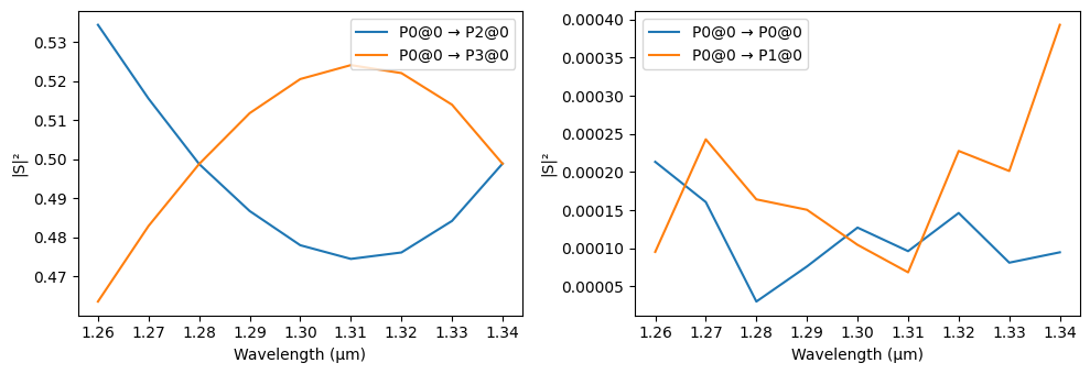
Rebuild the device from the optimized design vector and sweep the O-band again. Compare with the initial response above.
[9]:
dev_opt = bent_dc(r_bent=x[0], theta_deg=x[1], x_flat=x[2], x_rise=x[3], gamma=x[4])   # optimized device
print("optimized: r_bent=%.2f um, theta=%.2f deg, x_flat=%.2f um, x_rise=%.2f um, gamma=%.2f"
      % (x[0], x[1], x[2], x[3], x[4]))
s_opt = dev_opt.s_matrix(pf.C_0 / lams, model_kwargs={"inputs": ["P0"]})
pf.plot_s_matrix(s_opt)
dev_opt
optimized: r_bent=25.23 um, theta=8.45 deg, x_flat=4.12 um, x_rise=8.41 um, gamma=1.30
Uploading task 'P0@0…'
Starting task 'P0@0': https://tidy3d.simulation.cloud/workbench?taskId=fdve-77091d98-ef8e-4c73-a20c-3bbb1a027847
Downloading data from 'P0@0'…
Progress: 100%
[9]:

Fabrication robustness
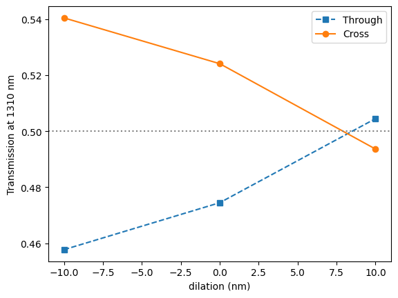
The real test is how the split holds up under dilation. We sweep the O-band at the three dilation corners for the optimized device, and compare the cross fraction at the center wavelength versus dilation for the optimized design.
[10]:
deltas = [-0.01, 0.0, 0.01]
corner_nm = [int(round(d * 1000)) for d in deltas]   # nm labels, consistent with deltas

# coupling spectra of the optimized device at each dilation corner
s02 = []
s03 = []
for dil in deltas:
    pf.config.default_technology.update(mask_dilation=dil)
    comp = bent_dc(r_bent=x[0], theta_deg=x[1], x_flat=x[2], x_rise=x[3], gamma=x[4])
    s = comp.s_matrix(pf.C_0 / lams, model_kwargs={"inputs": ["P0"]})
    s02.append(np.abs(s[("P0@0", "P2@0")][len(lams)//2 + 1]) ** 2)
    s03.append(np.abs(s[("P0@0", "P3@0")][len(lams)//2 + 1]) ** 2)

pf.config.default_technology.update(mask_dilation=0)

fig, ax = plt.subplots(1, 1)
ax.plot(corner_nm, s02, "s--", label="Through")
ax.plot(corner_nm, s03, "o-", label="Cross")
ax.axhline(0.5, color="grey", ls=":"); ax.legend()
ax.set_xlabel("dilation (nm)"); ax.set_ylabel("Transmission at %.0f nm" % (lam0 * 1000))
plt.show()
Uploading task 'P0@0…'
Starting task 'P0@0': https://tidy3d.simulation.cloud/workbench?taskId=fdve-80c50224-0a56-4028-ae0c-831b702f7a6b
Downloading data from 'P0@0'…
Progress: 100%
Progress: 100%
Uploading task 'P0@0…'Progress: 0% \
Starting task 'P0@0': https://tidy3d.simulation.cloud/workbench?taskId=fdve-7640144a-edd3-45de-8b6a-a90f22bbd1d8
Downloading data from 'P0@0'…
Progress: 100%