

Charge solver: a silicon electro-optic phase modulator#
In this notebook, we simulate a silicon electro-optic phase modulator. The numerical results are compared with the experimental data provided in [1]. The modulator consists of a pn-junction with a high doping contact to allow for a less resistive electrical interface.
The sketch below illustrates the main dimensions of the modulator:

Outline#
We start by setting up a
Chargesimulation intidy3d. For this example, the isothermal Drift-Diffusion (DD) equations are solved. A basic summary of the equations solved and nomenclature used can be found our td.SemiconductorMedium documentation.We show how the numerical results from this simulation can be used to determine the optical phase change.
References#
[1] Chrostowski L, Hochberg M. Silicon Photonics Design: From Devices to Systems. Cambridge University Press; 2015.
[2] Schroeder, D., T. Ostermann, and O. Kalz. “Comparison of transport models far the simulation of degenerate semiconductors.” Semiconductor science and technology 9.4 (1994): 364.
1. Construct our Charge Simulation#
GXRFWHRTb2Z0d2FyZQB3d3cuaW5rc2NhcGUub3Jnm+48GgAAHN1JREFUeJzt3XmYXFW19/Fv9ZxO AhkwIUCQgIxhSF6ZRLlcFBBQYPEKARJAZsIQAZkuMhgRBFRQgjJJUHhBEVEWqEgALyJIGAViDAQk ARISEjIP3Z0eqt4/9i49qVQ6XUXS1V39+zxPnqR27Vpn9elK96p99t4nZWaUO3c/E9jGzC7pYP/x wE7A6Wa2dEPmJh3n7gcAZ8SH95rZH0qZj4iIiBSnotQJdJJ3gSkd7Wxm44E5QN2GSkgKZ2ZPmdko 4AfA9qXOR0RERIpTVeoEOoOZPVXqHEREREQk6JQC1N2/A+wIPGdmE/K0/83Mbi4w5gHAWKA5/nkF mGpmf0n0GQlcFh8+bmZ3ryXWrsClQGVsmpCnTwVwOvBfQApIAz8ys1cLybscuPttwEDgYTP71bra OxhzOHARUEMYmX8NWGJmdxaR376E9wYx1mNm9v9y+nwmHq8/0Br/XGFmsxJ9+gE/BapjvM3iazYC bjGzp2O/jYArgGExTorw3ngxEWsUcBRwIXBN/DozwFVm9q+c3DYBrgIGxKYFwD+BB7NTQty9Gvgm sGs83irgOjN7u9Dztb64+8XAHsAbZnZtov0iYE9gipldU2DMQYRz0S82zQfeAn5pZisS/Y4HvhIf NgM3mNm0xPP9Cd/LKuBMYHP+872ckPNz43jgEMJ5TQG3mtmzheQtIiLt66xL8DcAHyeLTwAz+3b8 u9Disz/wLeAEMxttZicRConhOfFfi5dszwFGrCXWroTi4WwzOxY4kVAo7JXT9YfACjMbY2ajgXHA le7+pUJyLxM/Al7PLTLN7CwgVUTxuTNwOXB+PL/HEaZMXNb+K/PGOhwYBZxmZmOA44Fh7p5b+KwA rjSzY2K//wG+n/P1LInPfQCcCpwFnA0cSyhKs9qA283s6Jj7ScAV7l6ViPUgoUi8CDgr9rsQWO29 7+59gYnAzWZ2vJkdD9wRz0//RNeJhO9B9v14OXB7fD+Xyo2E/yPXJhvN7IdACznnd13cfWPgZ8CN iXMxEbgS2DjRL/t4dDyv5wNXuftuiRwWx/M0CziN8IHibOA4woeBbKyrCEXpCbH/6cBYdz+qkNxF RKR9nTICamYN7t4bwN23I4xWDiH8Qm4tImRL/Hsnd/+7mWUIv/z6FhHrYhKLjcys2d0vAf6R7eDu WwEVZnZ/ts3MFrv7KcD9wJ+LOG539g6wLYC7HwTcGh8PJsydLdTFwFgzW5ZtMLPH42KwQp0CHBnf E5hZG3C1u//F3evNrCG2fxTz7x8fz3X39uLWmtk5icdPJHJdCcxw93pgIzP7yN3fAQax5vm4PJHD XHdf4u7VZpZ9T59LGMl8NxH/TXe/AFgUc/488A8zm5ToM8fdzyEU0l/vyIla38wsHa8UZEcu3wOG mdk8oMrMmgsMeR5wtZnNTBzjn/FcLInHGQxsZWbfTfRZ7O6nEwr30Xni1pjZuYnHT8RY/QiLFa9O xFrh7qcBk4CHCsxfRETWojPngC6NIxqjCKMahwPTSBR6HRV/KXwdOAE43d17ATMIo5SFqsxd6W5m re4+OdE0HNjb3R/M8/p0Ecfs1sws4+64e4owWvx7YG9CwfVCESGrk8Vn4jj3FBIkXpbeBfh1nmIy DWwBvB37fo0wEvYe0OTudYRL6Gvz83aO+1lgPLAQWBA/bO1F/vdjU87j7CX7rJ3IM1JoZg8nHu4I HOrue3Qgfmeb6e7DgC8TPpgc7eGbMav9l+W1PWG6wmrMLFkI7gI8n6fP8vj+zGdt38ttgV3W9v/c 3SvMrMf9fxcR2RA6swB9kVCk7AkcA9xJGLEsuGCJo1ZzzOx7ibYDCXM3Ty0wXIW7p7IjZgmbJ/79 IfCMmV1aaK5l7B1CYb4JcDXh0nID4cNFoSrX3WXdzKzF3d+I0y7Wyt23Bo4EvpIsKNy9oKkD8TUV wPeAo8xseaL9xkJjRYsJ82jnt9PnXeB3ZnZLkcfYkCYD+wAHAmOAe4C5FPfBZBlh7ueidvrMAfZd y3OF/nx7F3jVzE4v8HUiIlKgztyGaTLh8uibZtZIKFYOBF4uItY4YP+ctjdYfY5cR03iPwtWgH8v cBqZfWxmrwOD40KZZL+KeDm0J5pMmIv3pJnNBjYlXL6c2f7L8nrO3U/KbXT3M9z90wXGesLd1/gQ 4u4js9NACCOhL+UUn58jjD4Wqh6Ym1N8bkl4bxfjl4T5i6uN3rn7f8f3JcCzwH+7++Y5fardPXfu cmd7ETgCWGhmTYT5s6MI75dC3U9YgLQadz/A3bP//98Cdo6jrsk+Y4GnCzmYmS0ijIZ/LidWyt2/ UFDmIiLSrpR14kb07j4H+KqZ/T3OHbzBzEau63V54lwMbEdYSPIuofjZnbCI5a3YpxK4G+gF1BKK i9diiPvN7JHYL0X4Jbc9YW7qtoRRqN6ES7JXmNmUOH3g+vj6twhFzHDCyuRfFPo1dHexmFsAfNrM 5rv7GcAhZnZkEbEqCJdatwJeIiwC2ZWwev3u2GcgcAthVGsAYeQ1u+L7x2b2fOyXIqwO3x14lTDK PhyYDVwUp1dUEy7DzgQ+BnaLsQ6Ij881s0XxPXpa4vnGeLzrzCz7XsLdvxtzfofwvkwTCtMhhIVO r8d5xWcTLhefZWZL3f1owp6mk8zszES8E4CjY982wgK6GcB3s/Mo3X0I4VL9wvh1DCO8h281s98X +C1Yr9z9H8A3zezJOD3hYTPbsshYJwNGOBdpwgfDt4Frs/Nm3X1T4MeEkdbZhJX4/wSuyV7ZaOd7 +b34ATN7vHrCe3FjwkK4IcDOhO9RVxxxFhHpljq1AF3f3H0A4Rf+YuDtPJfRC4m1MbAD8H52gcpa +vUn/KJfaGbvFHs8WZOH7Yx2IBRV78UFRMXGqiMUni3AW/kWwLj7DoRR8zeyC4M+wfGGAkOBd8zs 408SK8bLfmhqiTFXraXfIGAbwpSU9z/pcbuixLloJpyLvIuZ3H0zwlZZb1lii6Yij7kRYa7tUmD6 J/nZIiIia+oyBaj/5/aX7ZlrZud1QjryCbn7T4FPraNbwftCSvfm7hey5hZnuZabWaFzuUVEpBvp MgWoiIiIiPQM/16E1MMX1HQ57v6FfNvIaEGEdAZ3/3x2T888z61t1XmP4O77xDnmIiJSpOym0RWE RRnfbmfvPOkk8Zfb94Fbkt+P+O/bgGvXVhyIfFLxfTYeuCv3febuNwE3xYVcPU48N1cC96gIFREp XopQhN4NbA0c+kkn78v6ERdBTCJs1J9dIf0TwireQ5Lb/oisb3E1+KOEDeRPjXc5uo6wwfwBccui HikuivotsBIYY2bF3M1NRKRHSwG/AA4h3E5SP0i7lmrCfpL3xX+PAp5E3yfpHFXAl4A/EranOo3w /iv0lprlqJJwbv5sZmNKnYyISHdTRdjU+jDCRu5zS5uO5NiS8OHgb4QCdDRhRPTDUiYlPcYQwojn s4S7EZ1JuH3ueyXMqasYDBwM/LXUiYiIdEdVZjbR3dsItxM8wMymlTopAXfflTAP9Gwz+01sayFs uP1lM5tayvykvLn7dsBThA3l74ltownTdQ4zs2LuYFYW3P0zhLssXWFmd5Q6HxGR7ujf2zC5+ymE O7XsoU2XSysubvgHMN7MHsx57jjgMmBE8laSIutLXGjzCjAhW3wmnjPCB6Ph2TsR9STx3LwA3GVm Pyt1PiIi3dVq+4C6e18tbuka2vte6PskG5ref2vX079+EZH1QRvRi4iIiEin0l6SIiIiItKpVICK iIiISKdSASoiIiIinUoFqIiIiIh0qhRwNGGzc+naHjaz35c6Cel53P1gwl24uoLNgRpgZqkTiZ4w swdKnYT0PO7+X8BJpc5D1ul5M7trXZ3cPdXTtsCsAvbsU1u78W8uvLCy1MlIfudMnFg/Y968EYAK UCmFXYEh940b9/HAvn03KmUi33v44WF/n7uo7vBxdy7I93zTyqUNzz10/SsffzDtK8BGwMS9Dxu3 9YAh2w6s7dOvV21dn7pUZeV6ufLz8A9PyDQ1LtsLUAEqpbA9sM2oy34zp7KqpqrUyciannvo+sys NyfvB7RbgLr7JcB+7n6kmfWYWx1XAWzav/+Ug0eMGF/iXGQtRg4bNnHGvHmlTkN6tn+M2XffQ4Hh pUzipX/9a+q7LTOat9/z8KPW0uWtJyZeNJ9QNLdRUbHPwWdMGAH8n/WdS99NNr+yadayges7rkgB 3t5pn6NGET5sSRezeN7MCbPenDygvT7ufh5wIdACPOjuo3pKEao5oCJSLlbcd9WXn165dP5BwO3A 70inh91xwe4zgBUlzk1EZDWx+LwAuB74K5AGHnb32pIm1klUgIpIWWhuWvnMonkzd/nquNtPBFYC rVf8tuGlAZtuPbSpYdnrpc5PRCTL3fsARwD7AR8Tis9jgOXAZ0uYWqfRvBERKQs1db2/8o073gb4 7R9uGXsbQFVNrzOPvvTBfqXNTERkdWa2AvgigLvvG9tagGNLmVdnUgEqIuVmm779h9Q2N6+sAlR8 ioh0QboELyJlZ+DQHfr07TekptR5iIhIfipARaTs1Nb1rqqu662t5UREuigVoCJSdqpqelVW1dSp ABUR6aJUgIpI2amqra+qrqnL/fm2JJ1unVKShEREZDUqQEWk7FRX11VWVa8+AvrWC4/cdfUR1dNX LP7o3VLlJSIigQpQESk71bW9qiqqalf7+bbD3kd846BTfvj3ZYs+/KBUeYmISKBtmESk7FRV11VW 1a4xB7Rm2G5f/Oy7f5/0+qZb7VbfsOzjakgt6dN/0x2BIcUey937ASMIG0m/DjTG/fySfSqAnYDN galm9mHO8ylgKOFn8gdm1uruQ4FNgVfMLJMn1lBgupnNKDZ3EZFSUQEqImUnVVmZqqyoSuW2V9f0 6vvUPZc1P3XPZW8C/wts2e9TWzacf/f7ewCDizjUcOAnhNvoAZwLbOXuZmZzAGIheTOhOJ0FHOnu y4H/MbO2+LqNgLMIG1Mf6+6nAXWEOzodCXwrEesmYArwPvDlWACPM7PlReQvIlISKkBFpDylUmsU oFXVtfWVlVU7Xv7QytcqqmoOA6Zde1TvP86e/sLKLbbf+5hCwrc2N20J9Dezg7Jt7v4z4BGgMj6u IBSf55jZ3Njt5+7+NcI9oH8IYGZLgcvc/fvAXcB4M3s2ESM7SvpjQrE5J8a6190PIRSlpxeSf3vc vRdQpaJWRDYUFaAiUn4yrFF8AmTS6ZYvnvi9mRVVNd/Oth127p3XTH/xkQ+22H7vgg7R2rJqF+CV ZJuZZdz9VGBhbNoBeD1RfGb7/dbdH1hL6EvM7NVE33T851ZAG7CTu++U6N8C7F5Q8ut2GrAdMG49 xxURAbQISUTKVCpPDdrUuGzR4E/vvEWybeBm2w577al7ZhAKuQ7LZDK9gFW57Wb2caJoHATMLyRu O/3rgV7A1nn+3ObuGlAQkW5DP7BEpOykKvJ/tm5YvnBRW1vraveHT7e1tqxYPLeZFO+QYae8L8yj oqJiAWGR0BrcvZeZNRLmap4B3J7z/AAgk++17Zge/56YmDsqItItaQRURMpPKpWiYo05oJk3n//d v6b8773TgebY1jLlmfunAvWkMx9SgOq6Pi8Ae7v7rtk2dx/m7vcAewGY2SLgRXcf7+7Vsc/mwC+A axKvq3b3/oSFRxu7e//4598r+c2slVDI3hoXHmVf+zl3v6WQ3EVESk0joCJSlipSq3++bmtdtXCL bfc8Jp1uTa9qXDa7ttdGWzc3rvhX/023OfKQMyZUtKVbh1dWVnc8fkVFE/An4ER334xQ1C4AvpPc GsnMbnb3Q4G742XypcB5ZjYzEe7zwHHx38l5l7cRVs9nY/3R3d8HfuDuvQmX5V8Fru1w4iIiHeDu tUClmTVsiPgqQEWk7FTkubhTWVW7yYgDTtok2VbTq8+O+9g3sw/bVjUse2rF0vlzWletXNq6qrGx ublxZSaTztTU1tdX19b3rqyu69Ord/8tevcbtG98TZOZXbSufMzsMeCxdp7/C/CXjnxtZjaV9bji XUS6Jnc/Bjgc+ImZTS5BCmOAXQg7dqyTu19MuPoz1swWrKu/ClARKUsZ8q+Eb0fL0oWzmfPOywOa Vy7vvapxaVPD0oVNmVQm06vvwF51vTaqranvUzNgyLa9evcb1LRBkhYRiczs13EazqdKlMJ0YEVH O5vZD9z9B4SpROukAlREyk4mRSr3EnwH1A0autMBg4Z2eB2SiEjZMrO/bcj4KkBFREREuq56d58A bAL0BR4ws/uLCRRvgnESsIywr/AM4GUz+2Oiz27A2YSF6lPN7Oa1xPoCcH6MUwXck6dPNXAR4VJ+ hjA6+jMze1yr4EWk7KQqKlNUFHoFXkSkSzofuNHMRhPmhB7g7tsUGiTutHEWcKSZjTGzE4GPgNVi mdkbZnYmcDHhZhr5Yu1J2GLuBDM7BjgK2Bk4MKfrzcAbZjbazMYQ5pWOdvejVICKSNlJZTKF7rEp ItJV3WBm70O42xrwJDC8iDgNhLnxB8Xb7QJMBO4tItZ5wFlxv+NsXtcBrdkO7r4V0BgXYRL7NRGK 4LG6BC8iZSedSUNaNaiIlIXcG0+kKWIfdzNb5e7/lzBaeX3cT3g5ML6InCrMbGVO/Iy7J29PvA2w r7s/mOf1S1SAioiIiJQ5dx8CLDSziYm2XYBb+M8+xB2VcvfKPHdlS17On06YX3pOvgC6BC8iZSeV IZPOpNfdUUSk5ziFMIc0aQlQU0SsB4Arkw3ubiTmjJrZbCDj7v+V06/W3Q/XCKiIiIhIF+PuBwFj gTZ3X2Rmz7n7/oQ5lOnY9tcCQi4A9ol3ZvsQGAQMJixyyh6zgjAvtDdhZftnEpfQHzCz3wGYmbv7 YHd/FJgGbAFMBX4O/NTdx5vZa4QV8Fe5+1hgJrAZMBD4uQpQESk7adKkwpYfUgB3rzWzVetqE5EN z8yeAJ7IaXsaeLrIeHcAxFsCDwWWmdnCnD5p4OSOxnP3u4AtgXn5btkZFx19Kx5zS2CxmS0G7QMq IuUok9El+AK5+ybAS+5+RKJtM+DP7n6smb1RuuxEJB93v5Kwx2Z75pnZuOwDM2sljEZ+YnEO6Dpj xWPOSLapABUREcxsgbtfAkwibChdT9ju5X4VnyJdk5l9t9Q5FEuLkESk7GTSaUhrL9BCmdlDwAXE zaqB+8zsmtJmJSLlSCOg3cch7j6g1ElIj7Q7MLnUSXRR+7n7j0qdxAbwN2BjYFCZfn3lYGfgvVIn IVIsFaDdwKEjR74xbdas90qdh/RYkzbv3/814LBSJ9JhKTKZDbwGabs9DpuSbm0p14mmH5c6AVmn p+v7DpgGHFPqRESKoQK0Gzhl//0nnLL//qVOQ6R72cC34zzw5BseOfDkGzbkIUREypbmgIpI2cm0 tWXa0q2aAyoi0kWpABWRstPS3Njauqop9xZxIiLSRagAFZGy07qqsbW1ubFc52eKiHR7KkBFpOy0 tjS1pduaNQIqItJFqQAVkbLT3NTQ2qIRUBGRLksFqIiUnZbmhrbWpkaNgIqIdFEqQEWk7DQ3LG9t blqpAlREpIvSPqAiUm4y89+fsqy1tbkeyACpUickIiKr0wioiJSLNqAFmNK4cmlry6rGNLAAaAU0 H1REuhR3r+5IW7lSASoiZaG5acUfrj6i6v1bv7HLidm2JfPe+9Ft5+76XtPKJc+VMjcRkSR37wNM dffdE239gOfcfb/SZdZ5VICKSFmoqetz6Ofsgt/Mnzn1cWAwUP/j04Yd/6kthz9V17vfPqXOT0Qk y8xWAOcDfwC2AaqBx4HnzeyZUubWWVSAiki5qD7w5B+cOHjYbtcBpwOjhmw98tGjLv3VwWi+u4h0 MWb2J+AM4JvAAcBkM7ugtFl1niqA2QsX7v/9Rx99rNTJiIi056EXX9x5yaIVdZMfuWlSsj3d2tq2 qnFZS1PD0uZlC2ZtBUwG6jfdesSWk/2m6cD0UuQrIj3X60/+YmdgTnt9zOxRdz8R+IKZXdw5mXUN KWB/YK9SJyIi0gFDCZeqZpQ6kTK3DzCQcHkwU+JcRLqzqWb2h1In0RVVmdnTwNOlTkRERErP3c8B Pk/YPWAwcIGZqQgVkfVKc0BFRAQAdz8duBi4BXDgc8BN7q69VEVkvVIBKiIiuPsmwDmEaVkLgWbg y4QpWruWMDURKUMqQEVEBDNbAIw0s5mJtiXA583sjdJlJiLlSAWoiIgAkG+up+Z/isiGoAJURERE RDqVClARERER6VS6O4iIiHSIu18IfAq4wsxaO/G4hxG2hgK4z8ymdtaxRWTD0AioiIh01H3AZ4DK Tj7uM8CdwGxgu04+tohsACpARUSkQ8xsHrC8BMddZmYzgPmdfWwR2TB0CV5ERArVx92vAbYA5gLX mtnCYgK5+zDgfMKl/QbCKGsvM/tTEbFGAmcCfYGlwE/MbFpOn08DXyeMpKaAqcCNZtac6LMVMBZo M7PL3f0zMcca4Dtm9mHstzFwMrAbUEu47/cNZvZxItYYwi1kfw58B9gYeDv2a8jJbSPgm8C2hDtR /RlYYGaPJfpUAKcA+yXyv9nMGgs9XyKlpBFQEREp1ATgFjM7DrgXuL2YIO7+WeBaQjE2GrgAOBD4 VhGxjgLOAL5lZmNi3Gvd/Ss5XTcBHgVOjv1eA67O6TMLuAPYxd2PJNwdajxwHbBHot8A4FXgnJj/ RMJdpJIeAw4CLiXMnT0OeB64MSf//oTi+5GY16nxqQcSfVKE870U+LqZHR/z/1MsXkW6DRWgIiJS qIvM7AMAM3sdaHT3miLiXAqcZmZzYqzlwBXA44UEiaOCXwfONrNFMdaHwPHAZcm+Zvaqmb1uZi3x 8ePAp3P6tMUN+VsId4Eaa2YLzGymmXmi30wzezY7kmlmbwKZnFiLgRWEwnhBbJsEDMz5Mi4HLjGz 12KfVjO7F7ghGQ54xsx+Y2bpRKw7CSO/It2GLsGLiEihFuU8biH8PmnO0zcvd68CmnIvQ8eN768t MJ9hwDbAr90997lB7l6fPY67H0K4vN5IuOTfAPRbS9xmM/tOO1/DroTCMQOsirF2ztN1pZk15bS1 5TzezMzeyn2hmSXPxe7ACHc/MKdbHZofK92MClARESmFNtbf76CPgBfN7OT2OsVL/kcDo8xsVaL9 V4Ue0N37At8HxiTnvxYTK0p1oM9s4Ekz+0uRxxDpMnQJXkREOl0c6Wxw951yn3P3o929dwGxVgJN cUQyN9ZmiYcjgAdyis+RQP+Ckg+GAc/mFJ+bAsOLiAXwnLuPzm10973cfcf48GHgLHevzOmTcvch RR5XpCRSZlbqHEREpAtx93HAdmY2Lqf9JMIq7ccIC4cWu/vxhEU6k4Drs3MwO3icTQjzF18G3gAG ExYhvWBmE2KfYYTFRSlgByBNWEWeAe6MczWzK8h/TFhA9HKMtS9hWsCZZpaJxejPgHsIl8z3A5YB hxLmnY43s7S7fxX4AnA4YcES8bg/yc5Xdfdq4NfAn4APgc8CmwNbA68QFmnNjZv3nwo8SFhBn3H3 Y4GrYrxbY7wKwgKmZsK+p9XAF2Oel2aLZnffFzgv5vsRYTX/wcBtZvZwR8+9SKnpEryIiHTUH4G/ EoqxpbHtccKq7jSwpJBgZrbA3b9GWFm+HfABcHoc0cyaTSga85mViLUMOMXddyYsHJpPWCy1INFn Tiz+DgTqCdsvfejudwOZ7MIe4DlgGqE4TpqXiNXi7qOALxGK3d+a2TR3Hwz05j9zMn9JGLlsiaO+ AE8CLwErE/HSwDnuvj0wklAYf9vMVpvbaWbPuvurwJ6E7Z1eBiZ05p2pRNYHjYCKiMhq1jYC2oHX pQijguvypJmtragUkR7g/wM8y5XHIL019gAAAABJRU5ErkJggg==
- alt:
charge_modulator
[1]:
import numpy as np
import tidy3d as td
from matplotlib import pyplot as plt
from tidy3d import web
Specify our Modulator Dimensions#
Based on the figure above, we can define the dimensions of our electro-optic phase modulator. These are defaulted to micro-meters.
Since 2D problems are not yet supported, we will extrude our geometry in the z dimension. This is perpendicular to the plane of the problem in z_size \(\mu m\).
[2]:
# all units in um
w_core = 0.5
h_core = 0.22

w_clearance = 2.25
h_clearance = 0.09
w_side = 2.5
h_side = 0.22

w_contact = 1.2
h_contact = 0.5

z_size = h_clearance / 5
Create Multi-Physical Mediums#
In this example, we want to simulate the optical and electronic behaviour of this device. This means we need to specify material models that can represent the behaviour in these two physical domains.
The td.MultiPhysicsMedium was introduced in order to compose existing tidy3d medium models together into a unified multi-domain representation. td.MultiPhysics medium will be fully interoperable with any tidy3d simulation definition or class that uses existing medium definitions, and
should enable full flexibility in terms of creating unified material models progressively. In this example, we will focus on its usage for Charge simulations which it fully supports.
We still need to define a <Domain>Medium model for our Charge and Optical FDTD simulations. Let’s explore the different ways of doing this below.
Our silica (\(SiO_2\)) cladding behaves like an electronic insulator which can be defined with a td.ChargeInsulatorMedium. For the optical simulation, assuming we have an td.Medium frequency range valid to 0 Hz (electronic DC), we can reuse a the
td.material_library optical medium models and create a td.MultiPhysicsMedium accordingly:
[3]:
SiO2_optic = td.material_library["SiO2"]["Palik_LowLoss"]
SiO2 = td.MultiPhysicsMedium(
    optical=SiO2_optic,
    charge=td.ChargeInsulatorMedium(permittivity=np.real(SiO2_optic.eps_model(frequency=0))),
    name="SiO2",
)
11:26:14 UTC WARNING: frequency passed to 'Medium.eps_model()'is outside of
             'Medium.frequency_range' = (59958491600000.0, 1998616386666666.8)
However, in this example, we will create our own silica multi-physics model. The above td.material_library['SiO2']['Palik_LowLoss'] is not well defined for frequency=0. Hence, it is outside of the simulation validity region.
[4]:
SiO2 = td.MultiPhysicsMedium(
    optical=SiO2_optic,
    charge=td.ChargeInsulatorMedium(permittivity=3.9),  # redefining permittivity
    name="SiO2",
)
And now we define the remaining auxiliary mediums used to define our boundary conditions:
[5]:
aux = td.MultiPhysicsMedium(charge=td.ChargeConductorMedium(conductivity=1), name="aux")

air = td.MultiPhysicsMedium(heat=td.FluidSpec(), name="air")
A Drift-Diffusion Model defined in a td.SemiconductorMedium#
We will begin defining the electronic properties of the intrinsic semiconductor: i.e., the td.SemiconductorMedium without any doping.
Within a SemiconductorMedium, the Drift-Diffusion (DD) equations will be solved. In this example, we will explore an isothermal (constant temperature) case. This simulation performed at $ T=300 $ K. The DD equations, their assumptions, and limitations for this type of problem are discussed below:
The electrostatic potential \(\psi\), the electron \(n\) and hole \(p\) concentrations are computed from the following coupled system of PDEs.
The above system requires the definition of the generation-recombination rate \(R\) represented by our generation-recombination models and the flux functions (free carrier current density), \(\mathbf{J}_n\) and \(\mathbf{J}_p\). Their usual form is:
These depend on the carrier mobility for electrons \(\mu_n\) and holes \(\mu_p\) represented by our mobility models.
Where the effective field, defined in [2], is simplified to:
This approximation does not consider the effects of bandgap narrowing and degeneracy on the effective electric field \(\mathbf{F}_{n,p}\), which is acceptable for non-degenerate semiconductors. Bandgap narrowing models which are important for doped semiconductor effects can also be defined.
Material properties are defined as class parameters or other classes:
Symbol |
Parameter Name |
Description |
|---|---|---|
\[N_a\]
|
|
Ionized acceptors density |
\[N_d\]
|
|
Ionized donors density |
\[N_c\]
|
|
Effective density of states in the conduction band |
\[N_v\]
|
|
Effective density of states in valence band |
\[R\]
|
|
Generation-Recombination term |
\[E_g\]
|
|
Bandgap Energy |
\[\Delta E_g\]
|
|
Bandgap Narrowing |
\[\sigma\]
|
|
Electrical conductivity |
\[\varepsilon_r\]
|
|
Relative permittivity |
\[\varepsilon_0\]
|
|
Free Space permittivity |
\[q\]
|
|
Fundamental electron charge |
Our material library already has a silicon td.MultiPhysicsMedium model valid for a 300K isothermal case which incorporates a td.SemiconductorMedium. Note that its Shockley-Read-Hall recombination uses the doping- and temperature-dependent td.PalankovskiQuayApproxCarrierLifetime, which is supported by the accelerated charge solver only — reusing this medium with use_accelerated_solver=False raises a ValidationError. To run on the CPU charge solver, replace the SRH lifetimes
with constants or td.FossumCarrierLifetime.
[6]:
intrinsic_si = td.material_library["cSi"].variants["Si_MultiPhysics"].medium.charge
In case we want to build our own td.SemiconductorMedium, we can do so in the following manner (note that is identical to the one above):
[7]:
# Create a semiconductor medium with mobility, generation-recombination, and bandgap narrowing models.
intrinsic_si = td.SemiconductorMedium(
    permittivity=11.7,
    N_c=td.ConstantEffectiveDOS(N=2.86e19),
    N_v=td.ConstantEffectiveDOS(N=3.1e19),
    E_g=td.ConstantEnergyBandGap(eg=1.11),
    mobility_n=td.CaugheyThomasMobility(
        mu_min=52.2,
        mu=1471.0,
        ref_N=9.68e16,
        exp_N=0.68,
        exp_1=-0.57,
        exp_2=-2.33,
        exp_3=2.4,
        exp_4=-0.146,
    ),
    mobility_p=td.CaugheyThomasMobility(
        mu_min=44.9,
        mu=470.5,
        ref_N=2.23e17,
        exp_N=0.719,
        exp_1=-0.57,
        exp_2=-2.33,
        exp_3=2.4,
        exp_4=-0.146,
    ),
    R=[
        td.ShockleyReedHallRecombination(
            tau_n=td.PalankovskiQuayApproxCarrierLifetime(tau_max=1e-5, N_ref=1e16),
            tau_p=td.PalankovskiQuayApproxCarrierLifetime(tau_max=3e-6, N_ref=1e16),
        ),
        td.RadiativeRecombination(r_const=1.6e-14),
        td.AugerRecombination(c_n=2.8e-31, c_p=9.9e-32),
    ],
    delta_E_g=td.SlotboomBandGapNarrowing(
        v1=6.92 * 1e-3,
        n2=1.3e17,
        c2=0.5,
        min_N=1e15,
    ),
)
Create our doping regions#
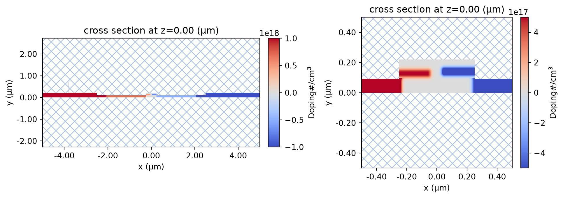
In our intrinsic silicon model above, we set the ionized acceptors \(N_a\) and ionized donor \(N_d\) density to zero. Since we will be doping our semiconductors with acceptors and donors, we need to create these doping distributions.
In this examples, we’ll use Gaussian doping boxes using the td.GaussianDoping model. The Gaussian doping concentration \(N\) is defined in the following manner:
\(N = N_{\text{max}}\) at locations more than
width\(\mu m\) away from the sides of the box.\(N = N_{\text{ref}}\) at locations on the box sides.
A Gaussian variation between \(N_{\text{max}}\) and \(N_{\text{ref}}\) at locations less than
widthµm away from the sides.
By definition, all sides of the box will have a concentration \(N_{\text{ref}}\) (except the side specified as the source), and the center of the box (width away from the box sides) will have a concentration \(N_{\text{max}}\).
[8]:
# doping with boxes
acceptor_boxes = []
donor_boxes = []

acceptor_boxes.append(
    td.ConstantDoping.from_bounds(rmin=[-5, 0, -np.inf], rmax=[5, 0.22, np.inf], concentration=1e15)
)

# p implant
acceptor_boxes.append(
    td.GaussianDoping.from_bounds(
        rmin=[-6, -0.3, -np.inf],
        rmax=[-0.15, 0.098, np.inf],
        concentration=7e17,
        ref_con=1e6,
        width=0.1,
        source="ymax",
    )
)

# n implant
donor_boxes.append(
    td.GaussianDoping.from_bounds(
        rmin=[0.15, -0.3, -np.inf],
        rmax=[6, 0.098, np.inf],
        concentration=5e17,
        ref_con=1e6,
        width=0.1,
        source="ymax",
    )
)

# p++
acceptor_boxes.append(
    td.GaussianDoping.from_bounds(
        rmin=[-6, -0.3, -np.inf],
        rmax=[-2, 0.22, np.inf],
        concentration=1e19,
        ref_con=1e6,
        width=0.1,
        source="ymax",
    )
)

# # n++
donor_boxes.append(
    td.GaussianDoping.from_bounds(
        rmin=[2, -0.3, -np.inf],
        rmax=[6, 0.22, np.inf],
        concentration=1e19,
        ref_con=1e6,
        width=0.1,
        source="ymax",
    )
)


# p wg implant
acceptor_boxes.append(
    td.GaussianDoping.from_bounds(
        rmin=[-0.3, 0, -np.inf],
        rmax=[0.06, 0.255, np.inf],
        concentration=5e17,
        ref_con=1e6,
        width=0.12,
        source="xmin",
    )
)

# n wg implant
donor_boxes.append(
    td.GaussianDoping.from_bounds(
        rmin=[-0.06, 0.02, -np.inf],
        rmax=[0.25, 0.26, np.inf],
        concentration=7e17,
        ref_con=1e6,
        width=0.11,
        source="xmax",
    )
)
Once we have our doping distributions, we can add it to our td.SemiconductorMedium and create our MultiPhysicsMedium to create our device structure with it. To include the doping to our semiconductor properties, we can implement this by creating a copy of it through the function updated_copy().
[9]:
Si_2D_doping = td.MultiPhysicsMedium(
    charge=intrinsic_si.updated_copy(
        N_d=donor_boxes,
        N_a=acceptor_boxes,
    ),
    name="Si_doping",
)
Compose our device structures#
We can now combine our medium definitions and geometry models to create our device structures.
[10]:
# create objects

oxide = td.Structure(
    geometry=td.Box(center=(0, h_core, 0), size=(10, 5, td.inf)), medium=SiO2, name="oxide"
)

core_p = td.Structure(
    geometry=td.Box(center=(-w_core / 4, h_core / 2, 0), size=(w_core / 2, h_core, td.inf)),
    medium=Si_2D_doping,
    name="core_p",
)

core_n = td.Structure(
    geometry=td.Box(center=(w_core / 4, h_core / 2, 0), size=(w_core / 2, h_core, td.inf)),
    medium=Si_2D_doping,
    name="core_n",
)

clearance_p = td.Structure(
    geometry=td.Box(
        center=(-w_core / 2 - w_clearance / 2, h_clearance / 2, 0),
        size=(w_clearance, h_clearance, td.inf),
    ),
    medium=Si_2D_doping,
    name="clearance_p",
)

clearance_n = td.Structure(
    geometry=td.Box(
        center=(w_core / 2 + w_clearance / 2, h_clearance / 2, 0),
        size=(w_clearance, h_clearance, td.inf),
    ),
    medium=Si_2D_doping,
    name="clearance_n",
)

side_p = td.Structure(
    geometry=td.Box(
        center=(-w_core / 2 - w_clearance - w_side / 2, h_side / 2, 0),
        size=(w_side, h_side, td.inf),
    ),
    medium=Si_2D_doping,
    name="side_p",
)

side_n = td.Structure(
    geometry=td.Box(
        center=(w_core / 2 + w_clearance + w_side / 2, h_side / 2, 0), size=(w_side, h_side, td.inf)
    ),
    medium=Si_2D_doping,
    name="side_n",
)

# create a couple structs to define the contacts
contact_p = td.Structure(
    geometry=td.Box(
        center=(-w_core / 2 - w_clearance - w_side + w_contact / 2, h_side + h_contact / 2, 0),
        size=(w_contact, h_contact, td.inf),
    ),
    medium=aux,
    name="contact_p",
)

contact_n = td.Structure(
    geometry=td.Box(
        center=(w_core / 2 + w_clearance + w_side - w_contact / 2, h_side + h_contact / 2, 0),
        size=(w_contact, h_contact, td.inf),
    ),
    medium=aux,
    name="contact_n",
)
A td.Scene helps us visualise that the structures are correctly positioned in this simulation.
[11]:
# create a scene with the previous structures
all_structures = [
    oxide,
    core_p,
    core_n,
    clearance_n,
    clearance_p,
    side_p,
    side_n,
    contact_p,
    contact_n,
]

scene = td.Scene(
    medium=air,
    structures=all_structures,
)


_, ax = plt.subplots(2, 1, figsize=(6, 6))

scene.plot(z=0, ax=ax[0])
scene.plot(y=h_core / 2, ax=ax[1])
plt.tight_layout()
plt.show()
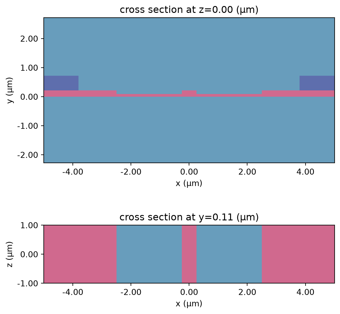
And to make sure our doping concentration regions are correct, we can visualize them with the convenience function plot_structures_property.
In the plots below, we have used property="doping", but we can also use property="acceptors" or property="donors" to check individual doping concentration regions.
[12]:
# plot doping from scene
_, ax = plt.subplots(1, 2, figsize=(12, 3.5))
scene.plot_structures_property(z=0, property="doping", ax=ax[0], limits=[-1e18, 1e18])
scene.plot_structures_property(
    z=0, property="doping", ax=ax[1], hlim=[-0.5, 0.5], vlim=[-0.5, 0.5], limits=[-5e17, 5e17]
);
Charge Boundary Conditions#
In this example, we will apply a DC voltage bias across the modulator junction at different voltages. We can do this by using the VoltageBC defined at both the p and n regions of the simulation region. This boundary condition accepts a td.DCVoltageSource model. This DCVoltageSource accepts a single float or an array of floats. In the latter case, a computation
result for each of the voltages defined in the array will be calculated.
The modulator will operate in reverse bias. This means a zero voltage is applied to the p side and a scalar positive voltage is applied to the n side.
[13]:
# create BCs
voltages = list(np.linspace(-0.5, 4, 19, endpoint=True))

bc_v1 = td.HeatChargeBoundarySpec(
    condition=td.VoltageBC(source=td.DCVoltageSource(voltage=0)),
    placement=td.StructureBoundary(structure=contact_p.name),
)

bc_v2 = td.HeatChargeBoundarySpec(
    condition=td.VoltageBC(source=td.DCVoltageSource(voltage=voltages)),
    placement=td.StructureBoundary(structure=contact_n.name),
)

boundary_conditions = [bc_v1, bc_v2]
Create our Monitors#
Monitors are used to determine exactly what data is to be extracted from the computation. In the case of a Charge simulation, we can extract electronic properties such as the potential \(\psi\), free carriers distribution \(\mathbf{J}\), and capacitance \(C\).
A td.SteadyCapacitanceMonitor is used to monitor small signal capacitance within the area/volume defined by the monitor.
The small signal-capacitance of electrons \(C_n\) and holes \(C_p\) is computed from the charge due to electrons \(Q_n\) and holes \(Q_p\) at an applied voltage \(V\) at a voltage difference \(\Delta V\) between two simulations.
Note that if only one solution is calculated (one single voltage data point is computed) the output for this monitor will be empty.
In order to extract the electrostatic potential \(\psi\) from our simulation, a td.SteadyPotentialMonitor results in a td.SteadyPotentialData.
A td.SteadyFreeCarrierMonitor let us record the steady-state of the free carrier concentration (\(\mathbf{J_n}\) electrons and \(\mathbf{J_p}\) holes) so that we can visualize results.
[14]:
# capacitance monitors
capacitance_global_mnt = td.SteadyCapacitanceMonitor(
    center=(0, 0.14, 0),
    size=(td.inf, td.inf, 0),
    name="capacitance_global_mnt",
)

# charge monitor around the waveguide
charge_3D_mnt = td.SteadyFreeCarrierMonitor(
    center=(0, 0.14, 0), size=(0.6, 0.3, td.inf), name="charge_3D_mnt", unstructured=True
)

# voltage monitor around waveguide
voltage_monitor_z0 = td.SteadyPotentialMonitor(
    center=(0, 0.14, 0),
    size=(0.6, 0.3, 0),
    name="voltage_z0",
    unstructured=True,
)

# Will be used later for the mode simulations
charge_monitor_z0 = td.SteadyFreeCarrierMonitor(
    center=(0, 0.14, 0),
    size=(td.inf, td.inf, 0),
    name="charge_z0_big",
    unstructured=True,
)
Mesh and Convergence criteria#
Before we can actually create the simulation object, we need to define some mesh parameters and convergence/tolerance criteria.
The Charge solver relies on a Finite Volume (FV) space discretization which is formally second order accurate in space. This convergence order is achieved if the mesh is “slowly varying”. In practice, this requirement translates in the fact that the mesh needs to be sufficiently fine in regions of spatially varying quantities of interest. In our case, carriers change rapidly in areas of rapidly varying doping which will need to be refined. Additionally, because carrier boundary layers are
created at insulator-semiconductor interfaces, these need to be refined. This is done naturally with the parameter dl_interface of the DistanceUnstructuredGrid class.
In the following, we define the mesh spacing as multiples of dl_boundaries which is, in turn, defined as 3% of h_clearance, or about one 33rd of that distance. This should give a sufficiently small element size to capture boundary layers at the interfaces as well as the depletion region in the waveguide core.
[15]:
dl_boundaries = h_clearance * 0.03
dist_boundaries = dl_boundaries * 2
dl_bulk = dl_boundaries * 40
dist_bulk = dist_boundaries * 40

ref_region_core = td.GridRefinementRegion(
    center=(0.0, h_core / 2, 0),
    size=(w_core, h_core, 0),
    dl_internal=dl_boundaries,
    transition_thickness=dist_bulk,
)

# mesh
mesh = td.DistanceUnstructuredGrid(
    dl_interface=dl_boundaries,
    dl_bulk=dl_bulk,
    distance_interface=dist_boundaries,
    distance_bulk=dist_bulk,
    relative_min_dl=0,
    sampling=500,
    non_refined_structures=[oxide.name],
    mesh_refinements=[ref_region_core],
)
Convergence settings are defined next though the ChargeToleranceSpec class which is an input to the IsothermalSteadyChargeDCAnalysis. In most cases, the default settings are sufficient. However, in cases with a large doping step as in the junction here, slightly more accurate results could be reached if the relative convergence tolerance is decreased. Here, we will set it to 1e-11.
One important thing to note here is that to run a Charge simulation we need to specify it in the HeatChargeSimulation class. We do this by specifying the parameter analysis_spec to an IsothermalSteadyChargeDCAnalysis since that is the type of analysis that we’re interested in running. Note that this class takes the argument convergence_dv. To understand how this parameter affects convergence, let’s imagine a case where we want to solve for 0 V and 20 V bias. In this case the
solver will first try to solve the 0V bias case and based off of this solution will go ahead and try to solve the 20V bias case. Since these are two very different biases, the solver may find it difficult to solve the second. By setting e.g.,convergence_dv=10 we’ll force the solver to go from 0V to 20V in 10V steps which eases convergence.
[16]:
convergence_settings = td.ChargeToleranceSpec(rel_tol=1e-11)

# Note: temperature in Kelvin
analysis_type = td.IsothermalSteadyChargeDCAnalysis(
    temperature=300, convergence_dv=10, tolerance_settings=convergence_settings
)
Create our HeatChargeSimulation#
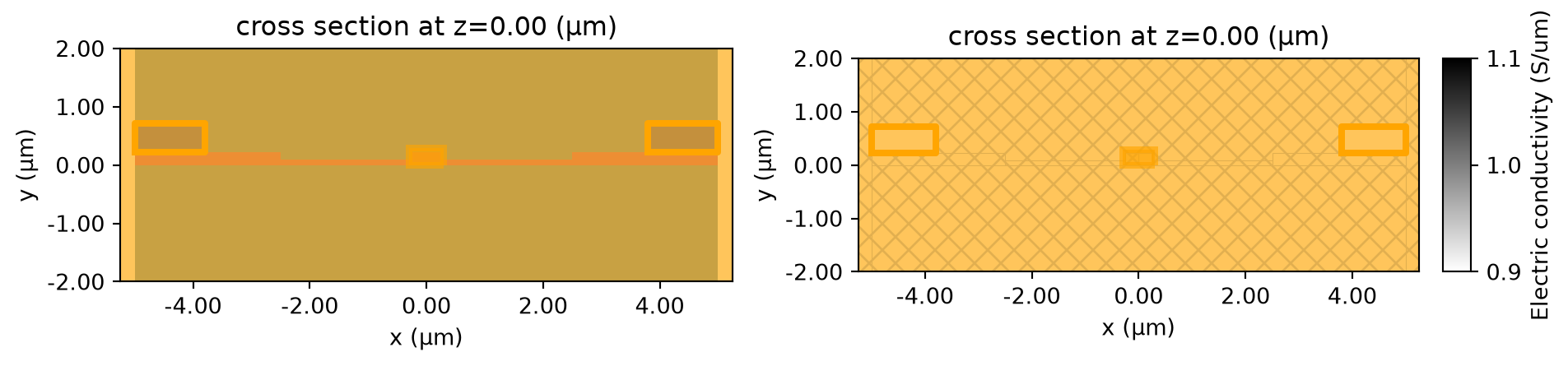
We’re now ready to create the actual simulation object.
[17]:
# build heat simulation object
charge_sim = td.HeatChargeSimulation(
    sources=[],
    monitors=[
        capacitance_global_mnt,
        charge_3D_mnt,
        voltage_monitor_z0,
        charge_monitor_z0,
    ],
    analysis_spec=analysis_type,
    center=(0, 0, 0),
    size=(10.5, 4, 0),
    structures=all_structures,
    medium=air,
    boundary_spec=boundary_conditions,
    grid_spec=mesh,
    symmetry=(0, 0, 0),
)

# plot simulation
fig, ax = plt.subplots(1, 2, figsize=(10, 15))
charge_sim.plot(z=0, ax=ax[0])
charge_sim.plot_property(z=0, property="electric_conductivity", ax=ax[1])
plt.tight_layout()
plt.show()
Run and visualize mesh#
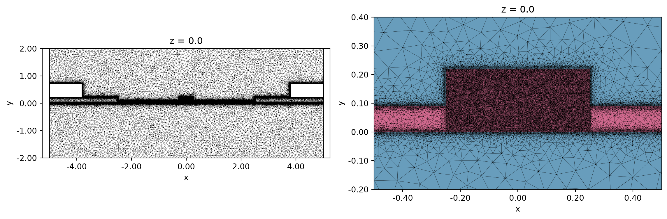
Before we submit the charge simulation for solving, we can inspect the mesh. This is particularly important here since the results for reverse-biased pn-junctions are usually very sensitive to the mesh especially in the depletion region, and since we have added many mesh refinement regions.
To visualize the mesh, we will build a VolumeMesher object using the simulation that we have defined, and a VolumeMeshMonitor covering the entire simulation plane.
[18]:
mesh_monitor = td.VolumeMeshMonitor(size=(td.inf, td.inf, 0), name="mesh")
mesher = td.VolumeMesher(
    simulation=charge_sim,
    monitors=[mesh_monitor],
)
[19]:
mesher_job = web.Job(simulation=mesher, task_name="charge_mesh")
mesher_data = mesher_job.run()
11:26:16 UTC Created task 'charge_mesh' with resource_id
             'vom-a782e087-ce48-4f80-9a41-ed1617380a83' and task_type
             'VOLUME_MESH'.
             Tidy3D's VolumeMesher solver is currently in the beta stage. Cost
             of VolumeMesher simulations is subject to change in the future.
11:26:17 UTC Estimated FlexCredit cost: 0.025. Use 'web.real_cost(task_id)' to
             get the billed FlexCredit cost after a simulation run.
11:26:18 UTC status = queued
             To cancel the simulation, use 'web.abort(task_id)' or
             'web.delete(task_id)' or abort/delete the task in the web UI.
             Terminating the Python script will not stop the job running on the
             cloud.
11:27:52 UTC starting up solver
running solver
11:28:03 UTC status = success
11:28:05 UTC Loading results from simulation_data.hdf5
[20]:
fig, ax = plt.subplots(1, 2, figsize=(12, 5))

# Mesh overlay over structures outlines only
mesher_data.plot_mesh("mesh", z=0, ax=ax[0], structures_fill=False)

# # Mesh overlay over structures plotted in false color
mesher_data.plot_mesh("mesh", z=0, ax=ax[1], structures_fill=True)
ax[1].set_xlim([-0.5, 0.5])
ax[1].set_ylim([-0.2, 0.4])

plt.tight_layout()
plt.show()
Run Simulation#
If we have already done the meshing for a solver, we can avoid redoing it by passing the task_id of the meshing task. If we don’t do that, a meshing task will be kicked off automatically before the solver task. Here, we will provide the meshing task_id. We can also estimate the cost of the simulation before running it.
[21]:
job = web.Job(
    simulation=charge_sim,
    task_name="charge_junction",
    parent_tasks=[mesher_job.task_id],
)
estimate_cost = job.estimate_cost()
11:28:08 UTC Created task 'charge_junction_solve' with resource_id
             'hec-8974785c-f999-42c6-b580-6d695a80b02d' and task_type
             'HEAT_CHARGE'.
             Tidy3D's HeatCharge solver is currently in the beta stage. Cost of
             HeatCharge simulations is subject to change in the future.
11:28:10 UTC Estimated typical FlexCredit cost: 0.101. For charge simulations,
             the billed cost depends on the number of solver iterations required
             for convergence.
             Maximum FlexCredit cost: 15.201. This assumes the charge solver
             reaches its configured iteration limits for all applied biases. Use
             'web.real_cost(task_id)' to get the billed FlexCredit cost after a
             simulation run.
             The FlexCredit estimate shown above is for the next workflow step
             'solve' only.
Note that a typical cost as well as a maximum cost is provided. These can differ quite a lot as the number of iterations needed for convergence can differ across simulations. However, it is very unlikely for the maximum cost to be reached, and the typical cost should serve as a better estimate.
Since HeatChargeSimulation is a multi-step workflow (meshing + solver), but we have already run the meshing, we can now run the solver step using either Job.step or Job.run. Here we use Job.step() to show the explicit solve step after a known mesher parent. If you rerun this cell after the solve has already completed, Job.step() has no incomplete workflow step to advance and may raise a DataError. In that case, use job.run(path=...) to continue or load the workflow
result, or load a completed job with Job.load() when returning to a saved task.
[22]:
charge_data = job.step(path="charge_junction.hdf5")
11:28:18 UTC status = queued
             To cancel the simulation, use 'web.abort(task_id)' or
             'web.delete(task_id)' or abort/delete the task in the web UI.
             Terminating the Python script will not stop the job running on the
             cloud.
11:28:35 UTC status = preprocess
11:28:53 UTC starting up solver
running solver
11:31:38 UTC status = success
11:31:45 UTC Loading results from charge_junction.hdf5
We can now examine the actual cost. It is higher than the typical estimate above, because strongly doped junctions operating in reverse bias can take more iterations to converge than typical. However, the cost is still well below the maximum cost.
[23]:
real_cost = web.real_cost(job.task_ids["solve"])
11:31:46 UTC Billed flex credit cost: 1.626.
Post-process Charge simulation#
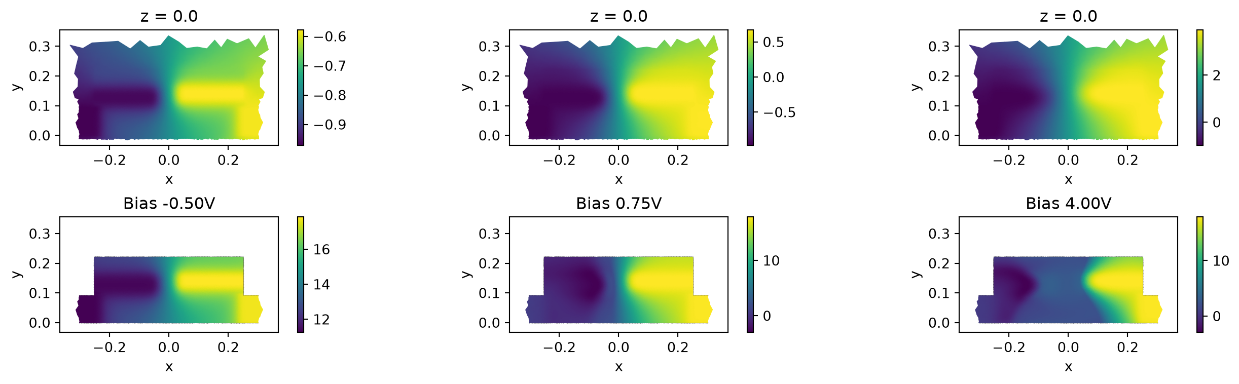
Let’s begin by visualizing the potential and electron fields at three different biases to make sure the solution looks reasonable. As it can be seen in the figure, as the (reverse) bias increases, the depletion region widens, as it is expected. The electric potential field also adapts to the applied biases and the amount of charge present in the waveguide area, which is also to be expected.
[24]:
voltages = charge_data[charge_3D_mnt.name].holes.values.voltage.data

fig, ax = plt.subplots(2, 3, figsize=(14, 4))
for n, index in enumerate([0, 5, 18]):
    # let's read voltage first
    charge_data[voltage_monitor_z0.name].potential.sel(voltage=voltages[index]).plot(
        ax=ax[0][n], grid=False
    )

    # now let's plot some electrons
    np.log10(charge_data[charge_3D_mnt.name].electrons.sel(z=0, voltage=voltages[index])).plot(
        ax=ax[1][n], grid=False
    )
    ax[1][n].set_title(f"Bias {voltages[index]:0.2f}V")

plt.tight_layout()
2. Experimental Data Validation#
In the second section of this example, we will validate the simulation numerical results with the experimental results from [1].
Small Signal Capacitance#
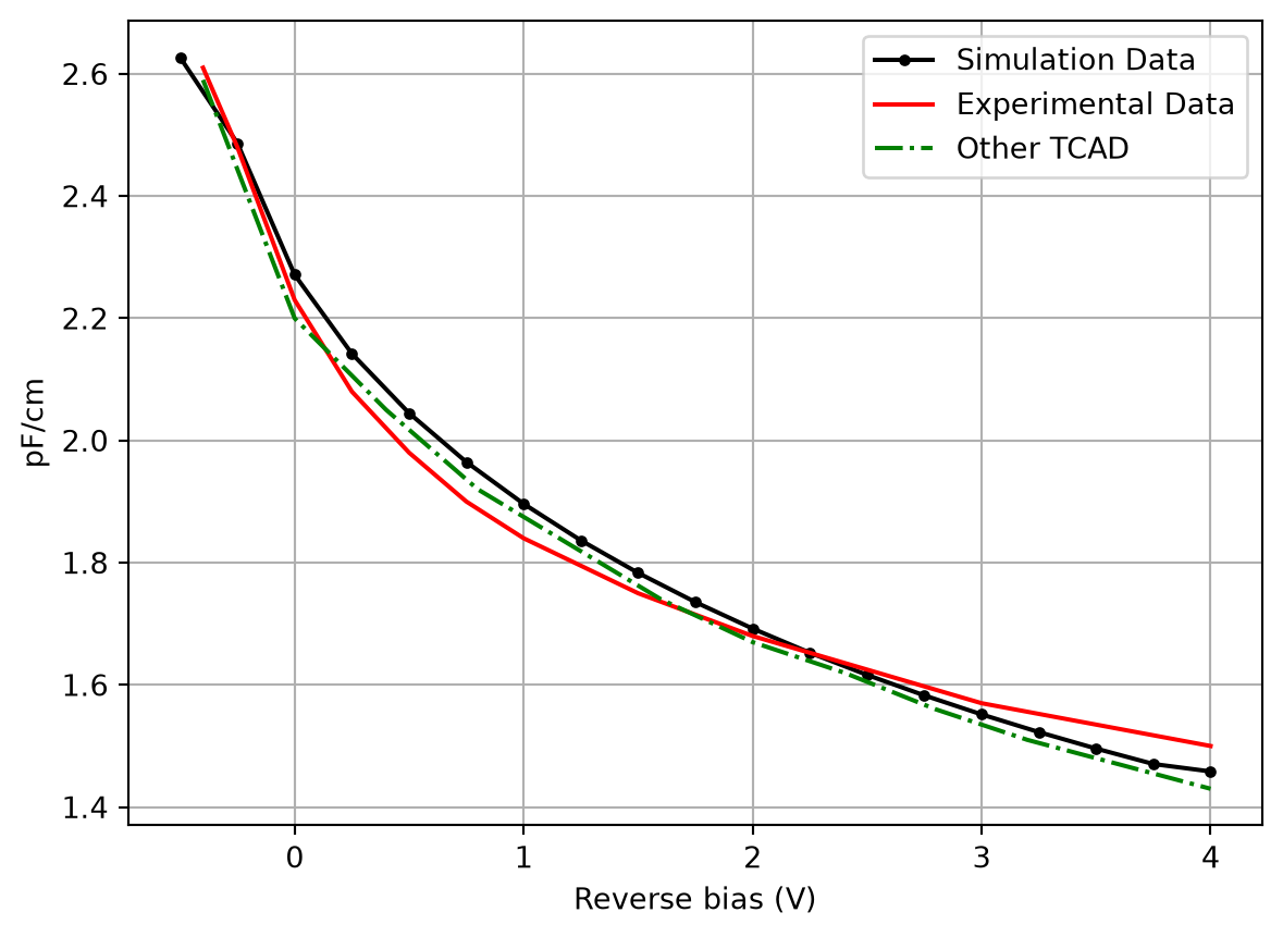
The td.HeatChargeSimulationData contains the extracted td.SteadyCapacitanceData specified by the monitor. The small signal capacitance is computed both with electrons and holes, and is averaged. As seen below, there is reasonable agreement between experimental data and simulation data (within the convergence tolerance).
[25]:
# capacitance from monitor - waveguide area
CV_baehrjones = [
    [-0.4, -0.25, 0, 0.25, 0.5, 0.75, 1, 1.5, 2, 3, 4],
    [0.261, 0.248, 0.223, 0.208, 0.198, 0.190, 0.184, 0.175, 0.168, 0.157, 0.150],
]

other_tcad = [
    [-0.4, 0.0, 0.4, 0.8, 1.2, 1.6, 2.0, 2.4, 2.8, 3.2, 3.6, 4],
    [0.259, 0.22, 0.205, 0.192, 0.183, 0.174, 0.167, 0.162, 0.156, 0.151, 0.147, 0.143],
]

mnt_v = np.array(charge_data[capacitance_global_mnt.name].electron_capacitance.coords["v"].data)
mnt_ce = np.array(charge_data[capacitance_global_mnt.name].electron_capacitance.data)
mnt_ch = np.array(charge_data[capacitance_global_mnt.name].hole_capacitance.data)

plt.plot(mnt_v, -0.5 * (mnt_ce + mnt_ch) * 10, "k.-", label="Simulation Data")
plt.plot(CV_baehrjones[0], np.array(CV_baehrjones[1]) * 10, "r-", label="Experimental Data")
plt.plot(other_tcad[0], np.array(other_tcad[1]) * 10, "g-.", label="Other TCAD")

plt.xlabel("Reverse bias (V)")
plt.ylabel("pF/cm")
plt.legend()
plt.grid()
Charge-to-Optical Coupling#
In this section, we will explore how we can couple the Charge simulation data into an optical FDTD simulation. This can be implemented by defining a medium perturbation. This means that optical medium properties such as the refractive index change e.g. \(\Delta n \propto \varepsilon(N_e, N_h)\) and optical loss \(\alpha \propto \sigma(N_e, N_h)\) are proportional to changes to the permittivity \(\varepsilon\) and conductivity \(\sigma\) by the free electrons \(N_e\) and free holes \(N_h\) density.
We start by defining the optical frequency range of interest:
[26]:
wvl_um = 1.55
freq0 = td.C_0 / wvl_um

fwidth = freq0 / 5
freqs = np.linspace(freq0 - fwidth / 10, freq0 + fwidth / 10, 201)
wvls = td.C_0 / freqs
We extract the real (\(n\)) and imaginary (\(k\)) parts of the refractive index from our silicon optical medium from our material library.
[27]:
si = td.material_library["cSi"]["Palik_LowLoss"]
n_si, k_si = si.nk_model(frequency=td.C_0 / wvl_um)
si_non_perturb = td.Medium.from_nk(n=n_si, k=k_si, freq=freq0)
Perturbation medium specifications#
To compute the perturbation, we will use empirical relationships presented in M. Nedeljkovic, R. Soref and G. Z. Mashanovich, “Free-Carrier Electrorefraction and Electroabsorption Modulation Predictions for Silicon Over the 1–14- μm Infrared Wavelength Range,” IEEE Photonics Journal, vol. 3, no. 6, pp. 1171-1180, Dec. 2011, which state that changes in \(n\) and \(k\) of Si can be described by formulas
where \(\Delta N_e\) and \(\Delta N_h\) are electron and hole densities.
For convenience this model has been implemented as NedeljkovicSorefMashanovich
We need to create an optical simulation. This means we need to slightly modify our existing Scene used in our HeatChargeSimulation. In order to do this, we will define the charge to optical coupling through a PerturbationMedium. This medium will enable us to input the numerical results from our HeatChargeSimulationData and change the optical medium properties.
Note that until we apply the carrier densities to the simulation the perturbation medium isn’t aware by how much permittivity/conductivity is going to change. This results in warnings every time the perturbation medium is added to a structure. Later in this notebook, when we apply the actual carrier concentrations, we can check by how much the permittivity is changing.
[28]:
perturbation_model = td.NedeljkovicSorefMashanovich(ref_freq=freq0)

si_perturb = td.PerturbationMedium.from_unperturbed(
    medium=si_non_perturb,
    perturbation_spec=td.IndexPerturbation(
        delta_n=perturbation_model.delta_n(),
        delta_k=perturbation_model.delta_k(),
        freq=freq0,
    ),
)

new_structs = []
for struct in charge_sim.structures:
    # NOTE: applying perturbation material to Si
    if struct.medium.name == Si_2D_doping.name:
        new_structs.append(struct.updated_copy(medium=si_perturb))

scene = td.Scene(
    medium=SiO2.optical,  # currently td.Simulation cannot accept a MultiphysicsMedium
    structures=new_structs,
)
Creating an Optical Mode Simulation#
Let’s create an optical mode simulation with our updated scene.
[29]:
span = 2 * wvl_um

port_center = (0, h_core, -span / 2)
port_size = (3, 3, 0)

buffer = 1 * wvl_um
sim_size = (13 + buffer, 10 + buffer, span)

bc_spec = td.BoundarySpec(
    x=td.Boundary.pml(num_layers=20),
    y=td.Boundary.pml(num_layers=30),
    z=td.Boundary.periodic(),
)

sim = td.Simulation(
    center=(0, 0, 0),
    size=sim_size,
    medium=scene.medium,
    structures=scene.structures,
    run_time=6e-12,
    boundary_spec=bc_spec,
    grid_spec=td.GridSpec.auto(min_steps_per_wvl=60, wavelength=wvl_um),
)

_, ax = plt.subplots(1, 2, figsize=(12, 6))
sim.plot(y=sim.center[1], ax=ax[0])
sim.plot(z=sim.center[2], ax=ax[1])

plt.tight_layout()
plt.show()

Coupling our SteadyFreeCarrierData into our PerturbationMedium:#
We already have configured our reference optical mode simulation with the default free carrier distribution. However, our td.HeatChargeSimulationData with our td.SteadyFreeCarrierData can be used to perturb our silicon optical medium. Let’s see how we can do this below. Note that we will be using a subset of the applied voltages to reduce the computational resources
We can create a list of perturbed optical simulation by using the function perturbed_mediums_copy():
[30]:
def apply_charge(charge_data, voltages):
    perturbed_sims = []
    for n, v in enumerate(voltages):
        e_data = charge_data[charge_monitor_z0.name].electrons.sel(voltage=v)
        h_data = charge_data[charge_monitor_z0.name].holes.sel(voltage=v)
        perturbed_sims.append(
            sim.perturbed_mediums_copy(
                electron_density=e_data,
                hole_density=h_data,
            )
        )
    return perturbed_sims


voltage_subset = [-0.5, 0, 1, 2, 3, 4]
perturbed_sims = apply_charge(charge_data, voltages=voltage_subset)
sim_zero_voltage = perturbed_sims[1]
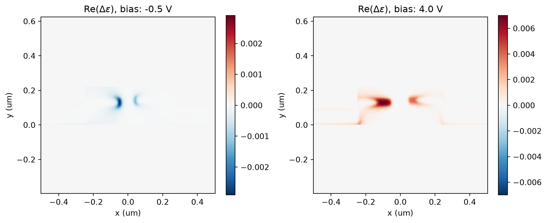
Let’s check what the difference in permittivity looks like at different applied voltages, compared to zero voltage.
[31]:
sampling_region = td.Box(center=(0, h_core / 2, 0), size=(1, 1, 1))
eps_zero_voltage = sim_zero_voltage.epsilon(box=sampling_region).sel(z=0, method="nearest")

_, ax = plt.subplots(1, 2, figsize=(10, 4))
for ax_ind, ind in enumerate([0, len(voltage_subset) - 1]):
    eps_doped = perturbed_sims[ind].epsilon(box=sampling_region).sel(z=0, method="nearest")
    eps_doped = eps_doped.interp(x=eps_zero_voltage.x, y=eps_zero_voltage.y)
    eps_diff = np.real(np.real(eps_doped - eps_zero_voltage))
    eps_diff.plot(x="x", ax=ax[ax_ind])

    ax[ax_ind].set_aspect("equal")
    ax[ax_ind].set_title(f"Re($\\Delta \\epsilon$), bias: {voltage_subset[ind]:1.1f} V")
    ax[ax_ind].set_xlabel("x (um)")
    ax[ax_ind].set_ylabel("y (um)")

plt.tight_layout()
plt.show()
Running Waveguide Mode Simulations#
Instead of running a full FDTD simulation, we will compute the modes of the waveguide. This is a smaller computation that will also highlight the influence of free carriers fields over the refraction coefficient.
We will compute the waveguide modes on a plane centered around the core section of the device:
[32]:
from tidy3d.plugins.mode import ModeSolver
[33]:
mode_plane = td.Box(size=port_size)

# visualize
ax = sim.plot(z=0)
mode_plane.plot(z=0, ax=ax, alpha=0.5)
plt.show()

[34]:
mode_solvers = dict()
for i, psim in enumerate(perturbed_sims):
    ms = ModeSolver(
        simulation=psim,
        plane=mode_plane,
        freqs=np.linspace(freqs[0], freqs[-1], 11),
        mode_spec=td.ModeSpec(num_modes=1, precision="single"),
        fields=[],
    )
    mode_solvers[str(i)] = ms
[35]:
# server mode computation
ms_batch_data = web.Batch(simulations=mode_solvers, reduce_simulation=True).run()
11:32:48 UTC Started working on Batch containing 6 tasks.
11:32:55 UTC Maximum FlexCredit cost: 0.087 for the whole batch.
             Use 'Batch.real_cost()' to get the billed FlexCredit cost after
             completion.
11:33:21 UTC Batch complete.
Relative Phase Change \(\Delta \phi\)#
Based on the computed effective refractive index \(n_{eff}\), we can now determine both phase shift \(\Delta \phi\) and \(\alpha\) optical loss per cm as a function of the applied bias voltage \(V_n\) using the following equations from [1]:
We compare this to simulation data from another popular simulation software.
[36]:
n_eff_freq0 = [md.n_complex.sel(f=freq0, mode_index=0).values for md in ms_batch_data.values()]

ind_V0 = 1
delta_neff = np.real(n_eff_freq0 - n_eff_freq0[ind_V0])
rel_phase_change = 2 * np.pi * delta_neff / wvl_um * 1e4
alpha_dB_cm = 10 * 4 * np.pi * np.imag(n_eff_freq0) / wvl_um * 1e4 * np.log10(np.exp(1))

# other results
v_other = [-0.5, 0, 0.4, 0.7, 1.5, 2.4, 3.8]
pc_other = [-0.91, 0, 0.6, 1, 1.8, 2.7, 3.6]
loss_other = [4.9, 4.55, 4.34, 4.15, 3.77, 3.41, 2.95]

_, ax = plt.subplots(1, 2, figsize=(12, 4))
ax[0].plot(voltage_subset, rel_phase_change, "k.-", label="Simulation Data")
ax[0].plot(v_other, pc_other, "r-", label="Other Software")
ax[0].set_xlabel("Reverse bias (V)")
ax[0].set_ylabel("Relative phase (rad/cm)")
ax[0].grid()
ax[0].legend()

ax[1].plot(voltage_subset, alpha_dB_cm, "k.-", label="Simulation Data")
ax[1].plot(v_other, loss_other, "r-", label="Other Software")
ax[1].set_xlabel("Reverse bias (V)")
ax[1].set_ylabel("Loss (dB/cm)")
ax[1].grid()
ax[1].legend()
plt.tight_layout()
plt.show()
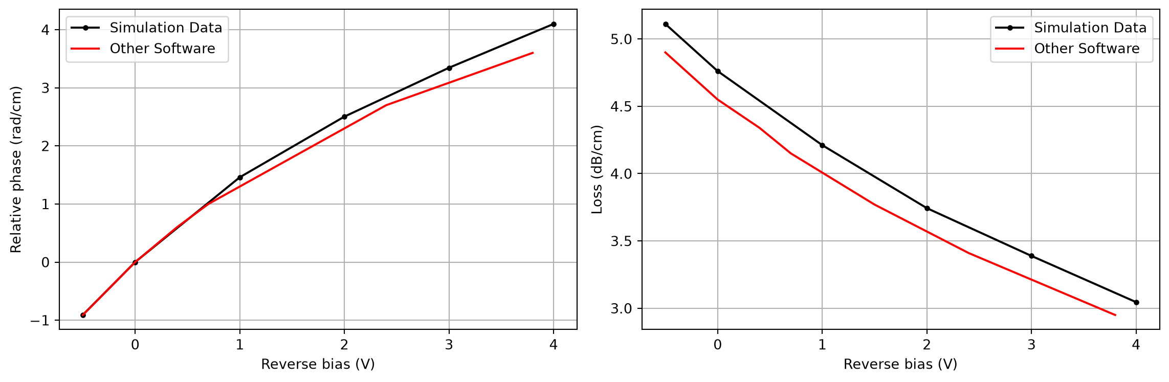
As it can be seen, we’d need to apply a bias of ~3V in order to get a phase shift of \(\pi\).
It is worth noting here that the refractive index and optical loss perturbations from the model in M. Nedeljkovic, R. Soref and G. Z. Mashanovich, “Free-Carrier Electrorefraction and Electroabsorption Modulation Predictions for Silicon Over the 1–14- μm Infrared Wavelength Range,” IEEE Photonics Journal, vol. 3, no. 6, pp. 1171-1180, Dec. 2011 change significantly at the specified wavelength of 1.55 \(\mu m\) and results will also change accordingly.