Importing GDS files#
In Tidy3D, complex structures can be defined or imported from GDSII files using Photonforge, Flexcompute’s photonic design automation tool. In this tutorial, we will illustrate how to use Photonforge to read a previously saved GDS file and import the structures into a simulation. For a tutorial on how to generate the GDS file used in this example, please refer to this notebook.
Note that this tutorial requires Photonforge, so grab it with pip install photonforge before running the tutorial or uncomment the cell line below.
We also provide a comprehensive list of other tutorials such as how to define boundary conditions, how to compute the S-matrix of a device, how to interact with tidy3d’s web API, and how to define self-intersecting polygons.
If you are new to the finite-difference time-domain (FDTD) method, we highly recommend going through our FDTD101 tutorials.
[1]:
# install photonforge
# !pip install photonforge

import matplotlib.pyplot as plt
import numpy as np
import photonforge as pf
import tidy3d as td
Loading a GDS file with Photonforge#
To load the geometry from a GDSII file, we use pf.load_layout, which reads the file and returns a dictionary of Component objects. We then use pf.find_top_level to automatically identify the top-level cell — the one that is not referenced as a sub-cell by any other cell in the file:
[2]:
gds_path = "misc/coupler.gds"

# Load all components from the GDS file
components = pf.load_layout(gds_path)

# Identify the top-level component (not referenced by any other cell)
top_level = pf.find_top_level(*components.values())[0]

print("Top-level component:", top_level.name)
print("Available cells:", list(components.keys()))
Top-level component: COUPLER
Available cells: ['COUPLER', 'COUPLER_ARM']
Inspecting Available Layers#
get_structures() extracts all 2D structures from the component (including flattened sub-cell references), grouped by (layer, datatype) pairs. This tells us which layers are present and how many structures each contains:
[3]:
structures_dict = top_level.get_structures()

for (layer, dtype), polys in structures_dict.items():
    print(f"Layer ({layer}, {dtype}): {len(polys)} polygon(s)")
Layer (0, 0): 1 polygon(s)
Layer (1, 0): 2 polygon(s)
We need to map each (layer, datatype) pair to a Tidy3D medium and vertical extent (slab_bounds). In this coupler layout, layer (0, 0) is the \(\text{SiO}_2\) substrate extending from z = -4 µm to z = 0, and layer (1, 0) contains the Si waveguide arms from z = 0 to z = wg_height.
We can also define fabrication-related parameters. We consider the waveguide sidewalls to be slanted by sidewall_angle — positive values model the typical fabrication scenario where the base of the waveguide is wider than the top. A small dilation accounts for proximity effects.
[4]:
# Define waveguide height and fabrication parameters
wg_height = 0.22
dilation = 0.02
sidewall_angle = np.deg2rad(10)

# Define materials
wg_n = 3.48  # Si refractive index
sub_n = 1.45  # SiO2 refractive index
medium_wg = td.Medium(permittivity=wg_n**2)
medium_sub = td.Medium(permittivity=sub_n**2)

# Map (layer, datatype) -> medium and extrusion parameters
layer_map = {
    (0, 0): dict(medium=medium_sub, slab_bounds=(-4.0, 0.0), sidewall_angle=0.0, dilation=0.0),
    (1, 0): dict(
        medium=medium_wg,
        slab_bounds=(0.0, wg_height),
        sidewall_angle=sidewall_angle,
        dilation=dilation,
    ),
}
Set up Geometries#
Each polygon from get_structures() exposes a to_polygon().vertices array that maps directly to td.PolySlab. We iterate over the layer map, skip any layers not in our map, and build a list of td.Structure objects. We also collect the arm geometries separately so we can compute the simulation bounding box from them later.
A positive sidewall_angle on the waveguide arms models a tapered cross-section — the base (z = 0) is wider than the top (z = wg_height) by dilation on each side, which is typical of real fabrication.
[5]:
arm_geos = []
structures = []

for (layer, dtype), polys in structures_dict.items():
    if (layer, dtype) not in layer_map:
        continue
    params = layer_map[(layer, dtype)]
    for poly in polys:
        geo = td.PolySlab(
            vertices=poly.to_polygon().vertices,
            axis=2,
            slab_bounds=params["slab_bounds"],
            sidewall_angle=params["sidewall_angle"],
            dilation=params["dilation"],
        )
        structures.append(td.Structure(geometry=geo, medium=params["medium"]))
        if (layer, dtype) == (1, 0):  # collect arm geometries for bounding box
            arm_geos.append(geo)

# Group arm geometries to compute simulation bounding box
arms_geo = td.GeometryGroup(geometries=arm_geos)
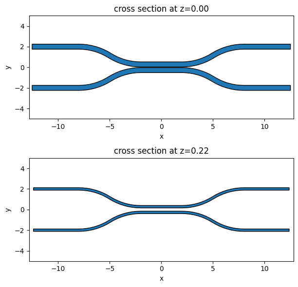
Let’s plot the base and the top of the coupler waveguide arms to make sure it looks ok. The base of the device should be larger than the top due to a positive sidewall_angle.
[6]:
f, ax = plt.subplots(2, 1, figsize=(15, 6), tight_layout=True)
arms_geo.plot(z=0.0, ax=ax[0])
arms_geo.plot(z=wg_height, ax=ax[1])

ax[0].set_ylim(-5, 5)
_ = ax[1].set_ylim(-5, 5)
Set up Simulation#
Now let’s set up the rest of the Simulation.
[7]:
# Spacing between waveguides and PML
pml_spacing = 1.0

# Simulation size
sim_size = list(arms_geo.bounding_box.size)
sim_size[0] -= 4 * pml_spacing
sim_size[1] += 2 * pml_spacing
sim_size[2] = wg_height + 2 * pml_spacing

sim_center = list(arms_geo.bounding_box.center)
sim_center[2] = 0

# grid size in each direction
dl = 0.020

### Initialize and visualize simulation ###
sim = td.Simulation(
    size=sim_size,
    center=sim_center,
    grid_spec=td.GridSpec.uniform(dl=dl),
    structures=structures,
    run_time=2e-12,
    boundary_spec=td.BoundarySpec.all_sides(boundary=td.PML()),
)
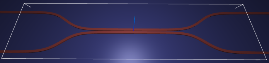
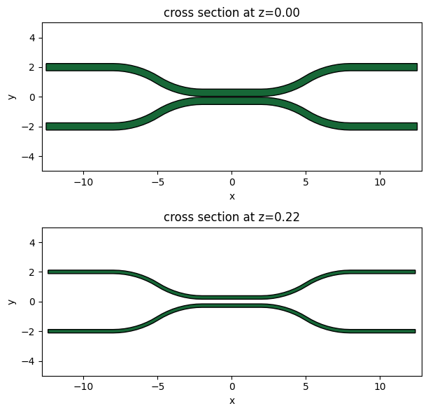
Plot Simulation Geometry#
Let’s take a look at the simulation all together with the PolySlabs added. Here the angle of the sidewall deviating from the vertical direction is 30 degree.
[8]:
fig, (ax1, ax2) = plt.subplots(1, 2, figsize=(17, 5))

sim.plot(z=wg_height / 2, lw=1, edgecolor="k", ax=ax1)
sim.plot(x=0.1, lw=1, edgecolor="k", ax=ax2)

ax2.set_xlim([-3, 3])
_ = ax2.set_ylim([-1, 1])