Broadband bi-level taper polarization rotator-splitter#
This notebook contains large simulations. Running the entire notebook will cost about 30 FlexCredits.
A polarization splitter-rotator (PSR) is a key component in silicon photonics that is used to manage the polarization state of light. It is a critical component in silicon photonic integrated circuits, enabling more complex and versatile photonic devices and systems. As the name suggests, the PSR has two main functions:
Splitting: It separates incoming light into its TE and TM components. This is useful because it allows each polarization to be processed separately, which can be important for certain applications.
Rotating: It can convert light from one polarization to another. For example, it can convert TE-polarized light to TM-polarized light, or vice versa. This is important because it allows the light to be correctly interfaced with other devices that might require a specific polarization.
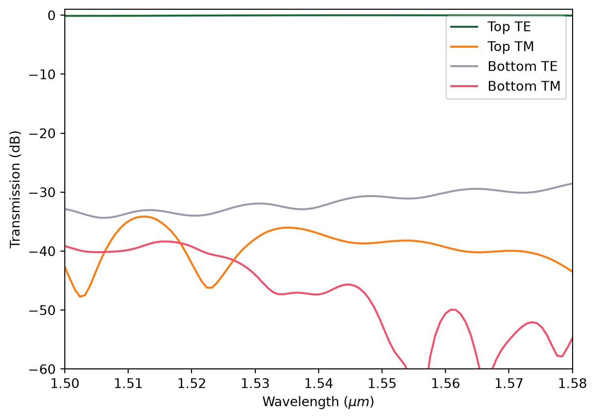
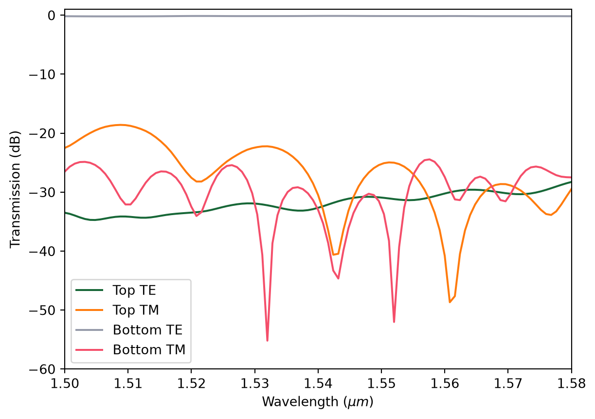
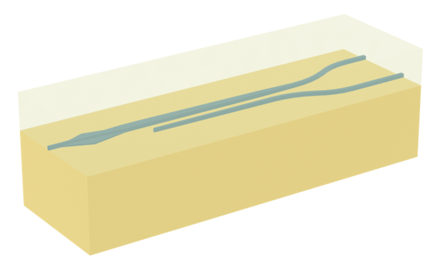
In another case study, we have introduced a compact PSR, which has a small footprint but narrow bandwidth. In the present study, we delve into the exploration of a broadband PSR. This device employs a bi-level taper to transition the TM0 mode input light into the TE1 mode. Subsequently, a long adiabatic coupler transforms this TE1 mode into the TE0 mode. Conversely, the TE0 input light primarily passes through the PSR with minimal alterations. The broadband PSR demonstrates superior bandwidth and insertion loss compared to the compact design, marking a significant improvement. However, it’s worth noting that this enhanced performance comes with a trade-off in terms of size. The broadband PSR has a considerably larger footprint, with a length longer than 0.5 mm, which causes a difficult simulation in conventional numerical tools. For Tidy3D, even such a large 3D full-wave simulation is fast.
The design is based on Wesley D. Sacher, Tymon Barwicz, Benjamin J. F. Taylor, and Joyce K. S. Poon, "Polarization rotator-splitters in standard active silicon photonics platforms," Opt. Express 22, 3777-3786 (2014), DOI: 10.1364/OE.22.003777.
For more integrated photonic examples such as the 8-Channel mode and polarization de-multiplexer, the 90 degree optical hybrid, and the broadband directional coupler, please visit our examples page. If you are new to the finite-difference time-domain (FDTD) method, we highly recommend going through our FDTD101 tutorials. FDTD simulations can diverge due to various reasons. If you run into any simulation divergence issues, please follow the steps outlined in our troubleshooting guide to resolve it.
[1]:
import gdstk
import matplotlib.pyplot as plt
import numpy as np
import tidy3d as td
import tidy3d.web as web
from tidy3d.plugins.mode import ModeSolver
Simulation Setup#
The simulation wavelength range is from 1500 nm to 1580 nm.
[2]:
lda0 = 1.54  # central wavelength
ldas = np.linspace(1.5, 1.58, 101)  # wavelength range of interest
freq0 = td.C_0 / lda0  # central frequency
freqs = td.C_0 / ldas  # frequency range of interest
fwidth = 0.4 * (np.max(freqs) - np.min(freqs))  # frequency width of the source
In this wavelength range, silicon and silicon oxide have minimal dispersion. Therefore, we use a constant refractive index for both.
[3]:
# define silicon and silicon dioxide media from material library
si = td.Medium(permittivity=3.47**2)
sio2 = td.Medium(permittivity=1.44**2)
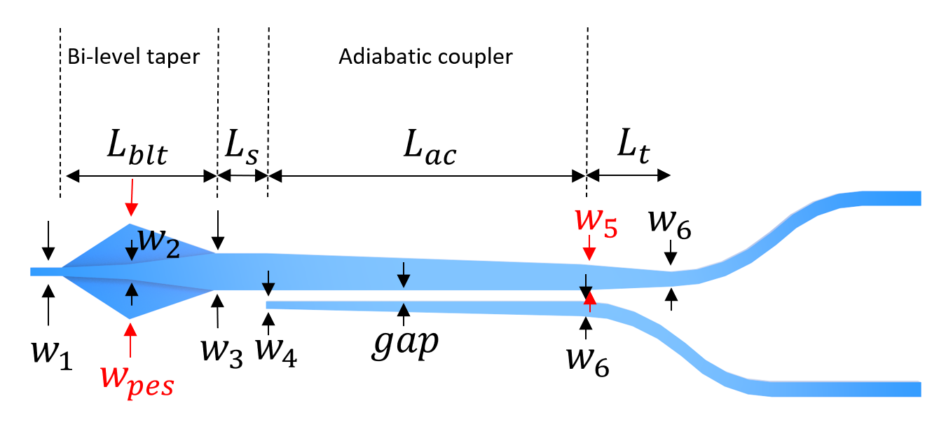
Define geometric parameters. The parameters are indicated in the figure below. In addition, we add a side wall angle to mimic realistic fabrication and see if this will degrade the device performance.
[4]:
L_blt = 100  # length of the bi-level taper
L_ac = 300  # length of the adiabatic coupler
L_s = 5  # length of the straight waveguide between the bi-level taper and the adiabatic coupler
L_t = 30  # length of the top waveguide taper after the adiabatic coupler

w_1 = 0.45  # input waveguide width
w_2 = 0.55  # waveguide width at the center of the bi-level taper
w_pes = 1.55  # width of the widest part of the partially etched slab
w_3 = 0.85  # waveguide width at the output of the bi-level taper
w_4 = 0.2  # waveguide width at the beginning of the bottom waveguide
w_5 = 0.65  # top waveguide width at the end of the adiabatic coupler
w_6 = 0.5  # output waveguide width
gap = 0.2  # gap size of the adiabatic coupler

t_pes = 0.09  # thickness of the partially etched slab
t_si = 0.22  # thickness of the silicon layer

inf_eff = 1e5  # effective infinity

sidewall_angle = 10 * np.pi / 180  # side wall angle
Define the partially etched slab structure.
[5]:
# define the partially etched slab
vertices = [
    (0, w_1 / 2),
    (L_blt / 2, w_pes / 2),
    (L_blt, w_3 / 2),
    (L_blt, -w_3 / 2),
    (L_blt / 2, -w_pes / 2),
    (0, -w_1 / 2),
]

partially_etched_slab = td.Structure(
    geometry=td.PolySlab(
        vertices=vertices,
        axis=2,
        slab_bounds=(0, t_pes),
        sidewall_angle=sidewall_angle,
    ),
    medium=si,
)
Define the waveguide structures using gdstk. For structures with bending parts, using gdstk is easy and convenient.
[6]:
R = 300  # bend radius
theta = np.pi / 30  # s bend angle

# define a gds cell
cell = gdstk.Cell("device")

# define the top waveguide using a path
top_wg = gdstk.RobustPath((-inf_eff, 0), w_1, layer=1, datatype=0)
top_wg.horizontal(0)
top_wg.horizontal(L_blt / 2, w_2)
top_wg.horizontal(L_blt, w_3)
top_wg.horizontal(L_blt + L_s)
top_wg.segment((L_blt + L_s + L_ac, (w_5 - w_3) / 2), w_5)
top_wg.horizontal(L_blt + L_s + L_ac + L_t)
top_wg.arc(R, -np.pi / 2, -np.pi / 2 + theta)
top_wg.arc(R, np.pi / 2 + theta, np.pi / 2)
top_wg.horizontal(inf_eff)
cell.add(top_wg)

# define the bottom waveguide using a path
bottom_wg = gdstk.RobustPath((L_blt + L_s, (-w_4 - w_3 - 2 * gap) / 2), w_4, layer=1, datatype=0)
bottom_wg.segment((L_blt + L_s + L_ac, (-w_3 - 2 * gap - w_6) / 2), w_6)
bottom_wg.arc(R, np.pi / 2, np.pi / 2 - theta)
bottom_wg.arc(R, -np.pi / 2 - theta, -np.pi / 2)
bottom_wg.horizontal(inf_eff)
cell.add(bottom_wg)

# define the waveguide tidy3d geometries
wg_geos = td.PolySlab.from_gds(
    cell,
    gds_layer=1,
    axis=2,
    slab_bounds=(0, t_si),
    sidewall_angle=sidewall_angle,
)

# define the waveguide tidy3d structures
wgs = [td.Structure(geometry=wg_geo, medium=si) for wg_geo in wg_geos]
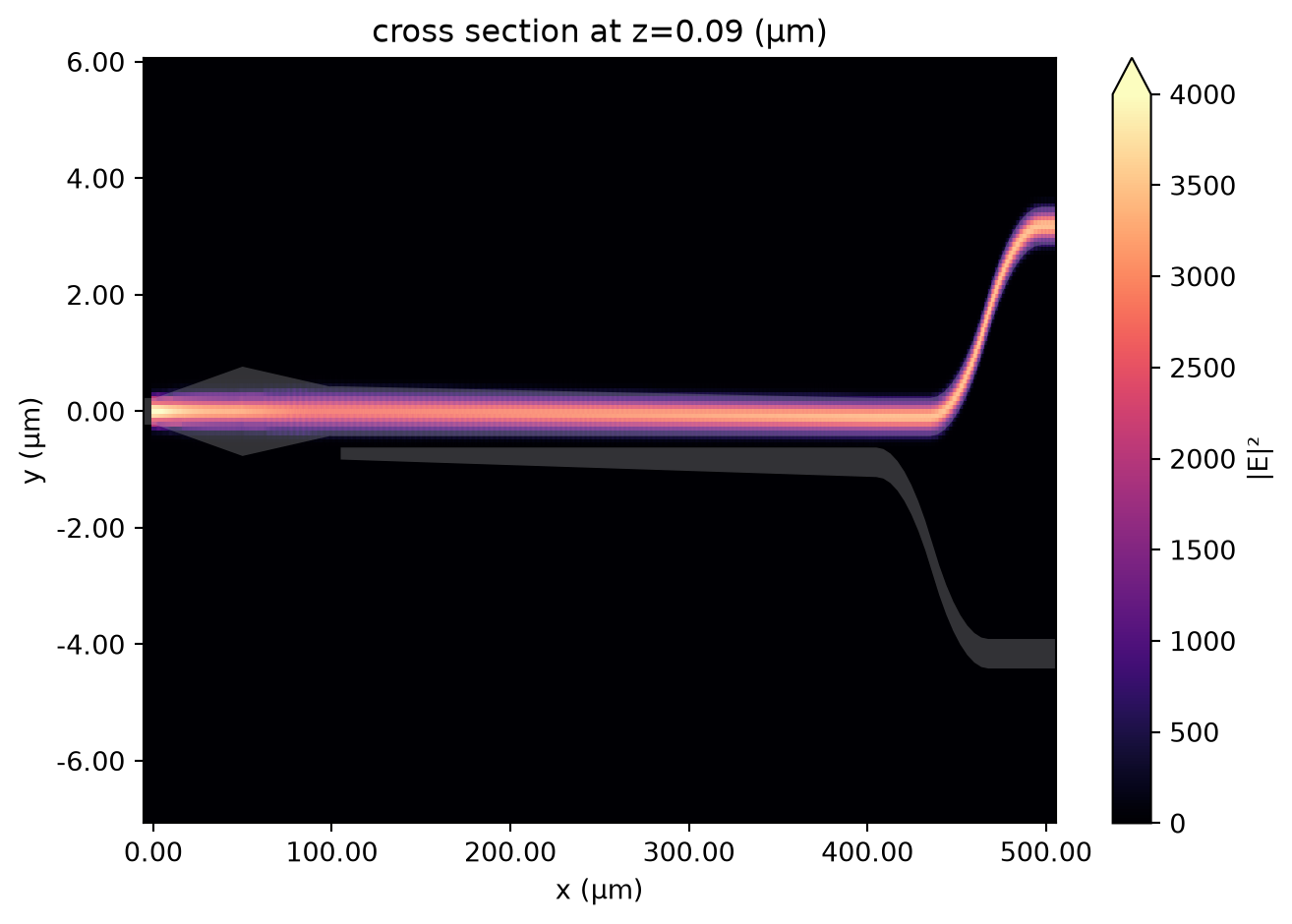
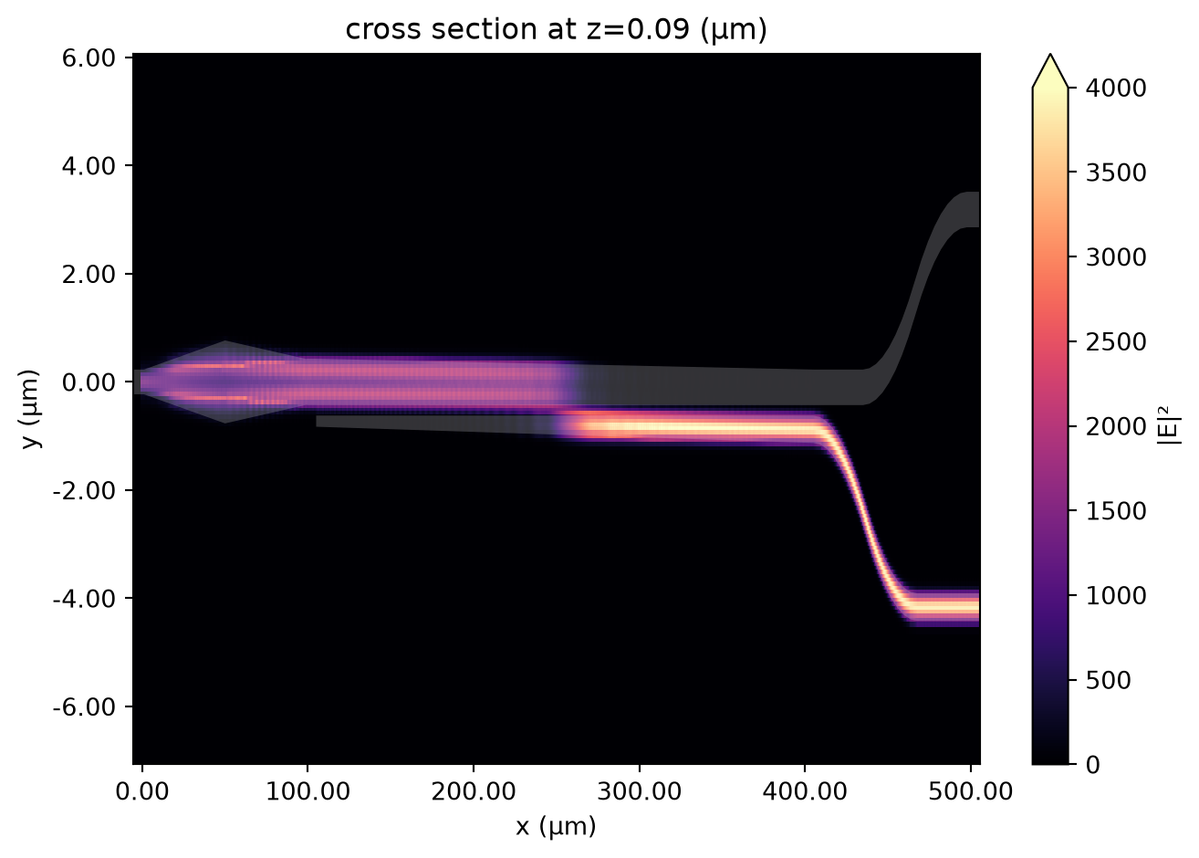
Define source, monitors, and simulation. Here we will define a ModeSource that launches the TE0 mode into the input waveguide. Two ModeMonitors are added to the top and bottom waveguides to monitor the transmission. A FieldMonitor is added in the \(xy\) plane to visualize the field distribution.
[7]:
run_time = 15e-12 # simulation run time
Lx = 510 # simulation domain size in x
Ly = 11 # simulation domain size in y
Lz = 9 * t_si # simulation domain size in z
x0 = 250 # simulation domain center in x
y0 = -0.5 # simulation domain center in y
z0 = t_si / 2 # simulation domain center in z
# define a mode source that launches the TE0 mode
mode_spec = td.ModeSpec(num_modes=2, target_neff=3.47)
mode_source_te = td.ModeSource(
center=(-lda0 / 2, 0, t_si / 2),
size=(0, 4 * w_1, 6 * t_si),
source_time=td.GaussianPulse(freq0=freq0, fwidth=fwidth),
direction="+",
mode_spec=mode_spec,
mode_index=0,
)
# define a mode monitor at the top waveguide output
mode_monitor_top = td.ModeMonitor(
center=(x0 + Lx / 2 - lda0, 3.2, t_si / 2),
size=mode_source_te.size,
freqs=freqs,
mode_spec=mode_spec,
name="mode_top",
)
# define a mode monitor at the bottom waveguide output
mode_monitor_bottom = td.ModeMonitor(
center=(x0 + Lx / 2 - lda0, -4.2, t_si / 2),
size=mode_source_te.size,
freqs=freqs,
mode_spec=mode_spec,
name="mode_bottom",
)
# define a field monitor to visualize field intensity distribution in the xy plane
field_monitor = td.FieldMonitor(
center=(0, 0, t_pes),
size=(td.inf, td.inf, 0),
freqs=[freq0],
interval_space=(2, 2, 1),
name="field",
)
# define simulation
sim_te = td.Simulation(
center=(x0, y0, z0),
size=(Lx, Ly, Lz),
grid_spec=td.GridSpec.auto(min_steps_per_wvl=12, wavelength=lda0),
structures=[partially_etched_slab] + wgs,
sources=[mode_source_te],
monitors=[mode_monitor_top, mode_monitor_bottom, field_monitor],
run_time=run_time,
boundary_spec=td.BoundarySpec.all_sides(boundary=td.PML()),
medium=sio2,
)
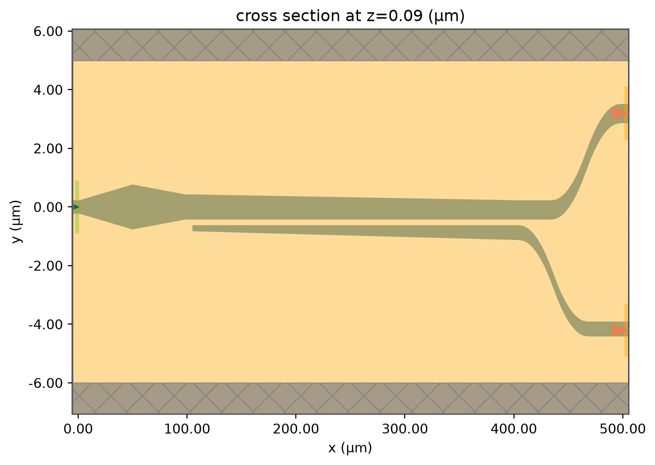
# visualize the simulation
ax = sim_te.plot(z=t_pes)
ax.set_aspect("auto")
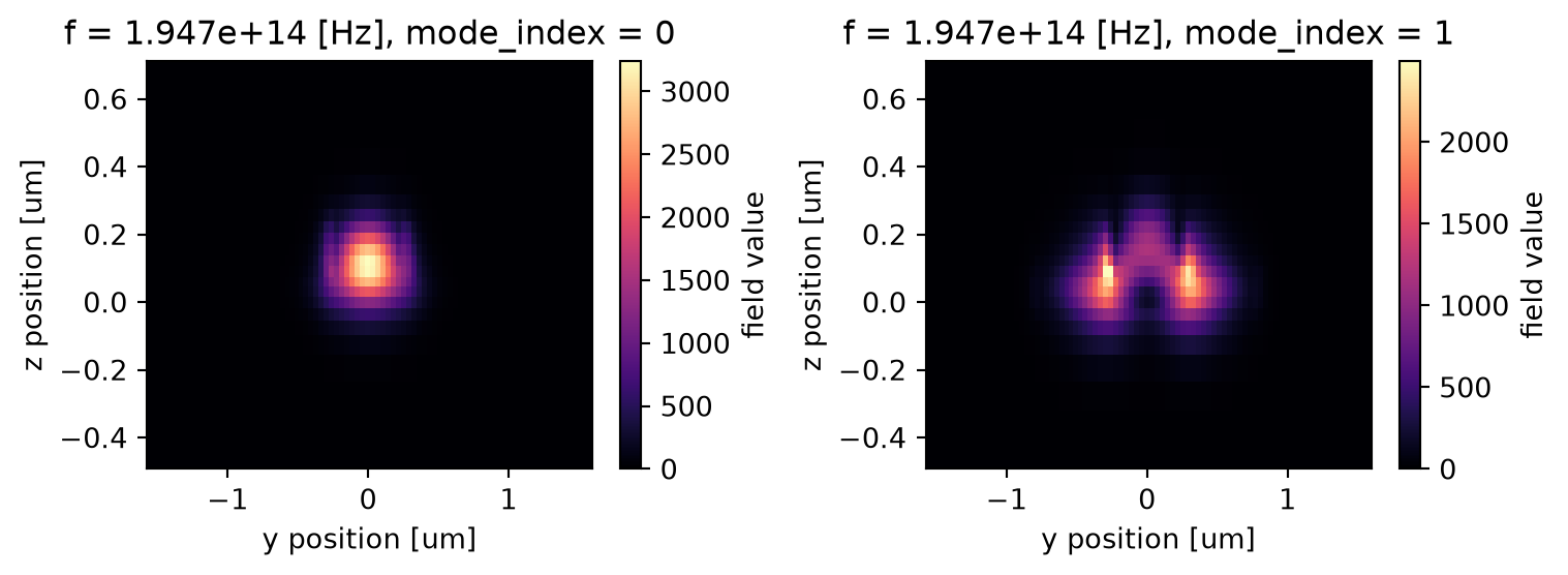
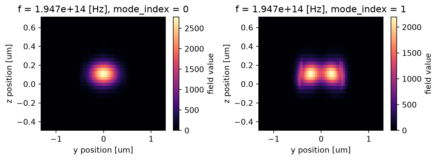
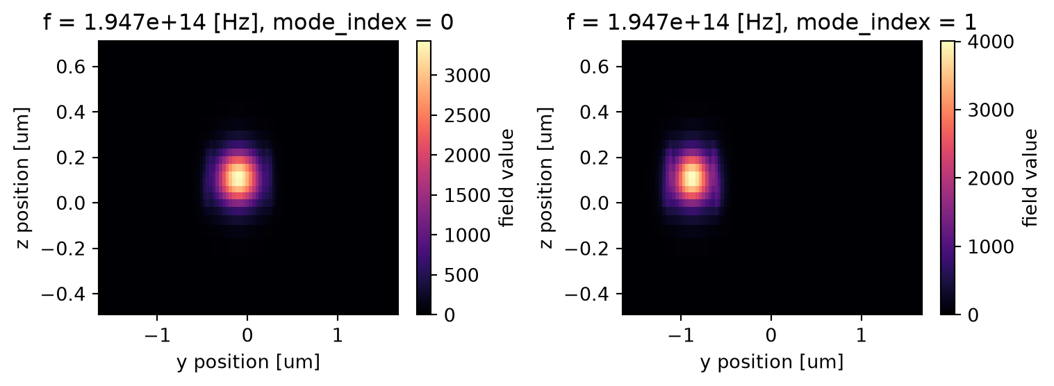
We can also visualize the cross sections at different \(x\) positions of the bi-level taper.
[8]:
fig, ax = plt.subplots(3, 1, figsize=(4, 7), tight_layout=True)

for i in range(3):
    sim_te.plot_eps(x=i * L_blt / 2, freq=freq0, ax=ax[i])
    ax[i].set_xlim(-1, 1)
    ax[i].set_ylim(-0.1, 0.3)
Mode Analysis#
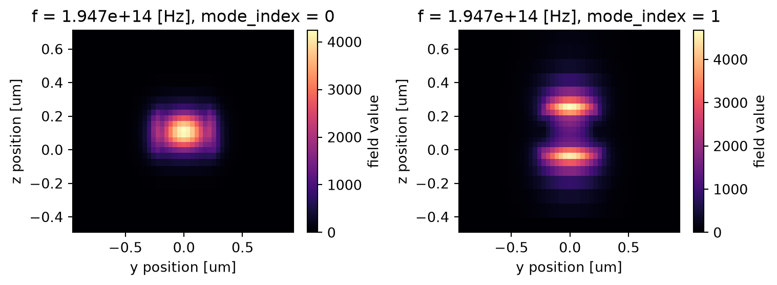
We can intuitively visualize the mode evolution alone the device to see physically why it functions as a PSR. This requires us to perform mode analysis at different \(x\) positions. First, let’s perform the mode analysis at the input waveguide (\(x=0\)) and solve for two modes.
As expected, the first mode is TE0 mode and the second mode is the TM0 mode. Note that the grid looks a bit coarse. If a finer resolution for the mode profile is needed, either use a finer grid or use Tidy3D’s waveguide plugin for the same analysis.
[9]:
mode_solver = ModeSolver(
    simulation=sim_te,
    plane=td.Box(center=(0, 0, t_si / 2), size=(0, 4 * w_1, 5 * t_si)),
    mode_spec=mode_spec,
    freqs=[freq0],
)
mode_data = mode_solver.solve()

fig, (ax1, ax2) = plt.subplots(1, 2, figsize=(8, 3), tight_layout=True)
mode_data.intensity.sel(mode_index=0).plot(x="y", y="z", cmap="magma", ax=ax1)
mode_data.intensity.sel(mode_index=1).plot(x="y", y="z", cmap="magma", ax=ax2)

mode_data.to_dataframe()