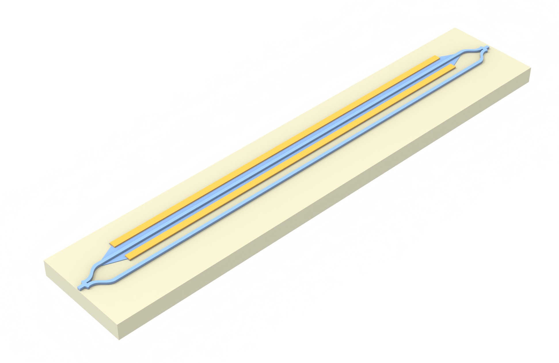
Carrier injection based Mach-Zehnder modulator#
Tidy3D capabilities include the modeling of material properties perturbations due to the presence of free carriers. This provides a convenient way to perform full-wave simulations of electro-optic modulators. In this notebook we demonstrate simulation of a simple pin-junction electro-optic modulator as part of an MZI. For generating free carrier distributions under different voltages we use our Charge solver. This example loosely follows the experimental modulator described in Zhou Liang et al 2011 Chinese Phys. Lett. 28 074202.
Problem Parameters#
[1]:
import numpy as np
import photonforge as pf
import tidy3d as td
from matplotlib import pyplot as plt
from tidy3d import web
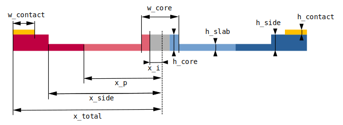
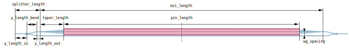
Our simulation setup will consist of an MZI with two arms, one of which has a common pin-junction profile. For combiner and splitter of the signal we use compact y-junction MMIs. The overall geometry and notation used is shown in the following figure.
[2]:
# modulator cross section parameters (um)
w_core = 0.5
h_core = 0.34
h_slab = 0.1
h_side = 0.34
w_contact = 0.5
x_side = 2.25
x_total = 3
x_i = 0.55
x_p = 1.75
h_contact = 0.1
# note that the height of the metal contact doesn't affect the results
# but devsim requires creating a region representing it
# in order to create a interface between the metal contact and modulator

# modulator doping concentrations (1/cm^3)
conc_p = 1e19
conc_pp = 5e19
conc_n = 1e19
conc_nn = 5e19
# note that concentrations in ++/-- are (conc_p + conc_pp) and (conc_n + conc_nn)

# photonic circuit geometric parameters (um)
y_length_in = 10
y_length_out = 1
y_length_bend = 10
wg_spacing = 3.5
taper_length = 10
pin_length = 200

# effective infinity
effective_inf = 1e6
Auxiliary variables for easier construction of simulations.
[3]:
mzi_length = 2 * taper_length + pin_length
splitter_length = y_length_in + y_length_out + y_length_bend

z_core = h_core / 2
z_slab = h_slab / 2
Semiconductor medium#
Before we can start the Charge simulation, let us create a semiconductor medium. Semiconductor mediums are constructed with the class SemiconductorMedium.
Since semiconductor mediums accept doping, let’s create those first. Doping is defined here in terms of boxes. Among the different types of doping boxes available we’ll be using here the ConstantDoping, which applies a constant doping to the doping box. One thing to note is that these doping boxes are additive, i.e., if two donor doping boxes overlap, the total concentration in the overlap region will be the sum of these two overlapping doping boxes. To further demonstrate this concept:
[4]:
acceptors = []
donors = []

acceptors.append(
    td.ConstantDoping.from_bounds(
        rmin=[-effective_inf, wg_spacing / 2 - x_total, -1],
        rmax=[effective_inf, wg_spacing / 2 - x_p, h_side + 1],
        concentration=conc_pp,
    )
)
acceptors.append(
    td.ConstantDoping.from_bounds(
        rmin=[-effective_inf, wg_spacing / 2 - x_total, -1],
        rmax=[effective_inf, wg_spacing / 2 - x_i, h_side + 1],
        concentration=conc_p,
    )
)

donors.append(
    td.ConstantDoping.from_bounds(
        rmin=[-effective_inf, wg_spacing / 2 + x_p, -1],
        rmax=[effective_inf, wg_spacing / 2 + x_total, h_side + 1],
        concentration=conc_nn,
    )
)
donors.append(
    td.ConstantDoping.from_bounds(
        rmin=[-effective_inf, wg_spacing / 2 + x_i, -1],
        rmax=[effective_inf, wg_spacing / 2 + x_total, h_side + 1],
        concentration=conc_n,
    )
)
[5]:
# let's define a material here for our Charge simulations
si_doped = td.MultiPhysicsMedium(
    optical=td.material_library["cSi"]["Li1993_293K"],
    charge=td.SemiconductorMedium(
        permittivity=11.1,
        N_c=td.ConstantEffectiveDOS(N=2.86e19),
        N_v=td.ConstantEffectiveDOS(N=3.1e19),
        E_g=td.ConstantEnergyBandGap(eg=1.11),
        mobility_n=td.ConstantMobilityModel(mu=400),
        mobility_p=td.ConstantMobilityModel(mu=200),
        R=[td.ShockleyReedHallRecombination(tau_n=1e-8, tau_p=1e-8)],
        N_a=acceptors,
        N_d=donors,
    ),
)
Optic mediums#
Since some of the structures will be reused in the optic simulations, let us also create the required mediums here.
[6]:
wvl_um = 1.55
freq0 = td.C_0 / wvl_um

si = si_doped.optical
n_si, k_si = si.nk_model(frequency=td.C_0 / wvl_um)

si_non_perturb = td.Medium.from_nk(n=n_si, k=k_si, freq=freq0)

sio2 = td.Medium(permittivity=1.444**2)
Charge simulation#
We are now ready to create the charge simulation. The first step is to create the waveguide structures. To do this, we define the following functions that encapsulate the necessary steps.
We will use PhotonForge’s layout capabilities. PhotonForge also provides a complete set of tools for photonic design automation, including PDK integration, parametric components, connectivity management, and technology definitions. You can check the many applications of this powerful tool here.
The make_waveguide function is a generic function that creates a tapered waveguide with initial width wg_width_0 and final width wg_width_1. This is easily achieved using pf.Path and pf.Path.segment.
[7]:
def make_waveguide(
    x0, y0, z0, x1, y1, wg_width_0, wg_width_1, wg_thickness, medium, sidewall_angle=0
):
    """
    Linear waveguide taper using PhotonForge.
    """

    # create path starting at (x0, y0)
    path = pf.Path(origin=(x0, y0), width=wg_width_0)

    # linear taper to (x1, y1)
    path.segment((x1, y1), width=wg_width_1)

    # convert to polygon
    poly = path.to_polygon()

    # create PolySlab geometry
    geometry = td.PolySlab(
        vertices=poly.vertices,
        axis=2,
        slab_bounds=(z0, z0 + wg_thickness),
        sidewall_angle=sidewall_angle,
    )

    return td.Structure(geometry=geometry, medium=medium)
[8]:
def make_rib_waveguide(
    x0,
    y0,
    z0,
    x1,
    y1,
    core_width,
    slab_width,
    side_width,
    core_thickness,
    slab_thickness,
    side_thickness,
    medium,
    sidewall_angle=0,
):
    """
    This function defines a linear waveguide taper and returns the tidy3d structure of it.

    Parameters
    ----------
    x0: x coordinate of the waveguide starting position (um)
    y0: y coordinate of the waveguide starting position (um)
    z0: z coordinate of the waveguide bottom surface (um)
    x1: x coordinate of the waveguide end position (um)
    y1: y coordinate of the waveguide end position (um)
    core_width: width of the waveguide core (um)
    slab_width: width of the slab (um)
    side_width: width of the side ribs (um)
    core_thickness: thickness of the waveguide core (um)
    slab_thickness: thickness of the slab (um)
    side_thickness: thickness of the side ribs (um)
    medium: medium of the waveguide
    sidewall_angle: side wall angle of the waveguide (rad)
    """

    # modulator
    slab = make_waveguide(
        x0=x0,
        y0=y0,
        z0=z0,
        x1=x1,
        y1=y1,
        wg_width_0=slab_width,
        wg_width_1=slab_width,
        wg_thickness=slab_thickness,
        medium=medium,
        sidewall_angle=sidewall_angle,
    )

    core = make_waveguide(
        x0=x0,
        y0=y0,
        z0=z0,
        x1=x1,
        y1=y1,
        wg_width_0=core_width,
        wg_width_1=core_width,
        wg_thickness=core_thickness,
        medium=medium,
        sidewall_angle=sidewall_angle,
    )

    y_side_top = y0 + (slab_width / 2 - side_width / 2)
    y_side_bottom = y0 - (slab_width / 2 - side_width / 2)

    side_top = make_waveguide(
        x0=x0,
        y0=y_side_top,
        z0=z0,
        x1=x1,
        y1=y_side_top,
        wg_width_0=side_width,
        wg_width_1=side_width,
        wg_thickness=side_thickness,
        medium=medium,
        sidewall_angle=sidewall_angle,
    )

    side_bottom = make_waveguide(
        x0=x0,
        y0=y_side_bottom,
        z0=z0,
        x1=x1,
        y1=y_side_bottom,
        wg_width_0=side_width,
        wg_width_1=side_width,
        wg_thickness=side_thickness,
        medium=medium,
        sidewall_angle=sidewall_angle,
    )

    return [core, slab, side_top, side_bottom]
With the above functions we can now create the waveguide structures pin_wg. For ease in defining boundary conditions we define here some auxiliary structures made up of a conductive medium defined with ChargeConductorMedium.
[9]:
# top arm: PIN region
pin_wg = make_rib_waveguide(
    x0=-pin_length / 2,
    y0=wg_spacing / 2,
    z0=0,
    x1=pin_length / 2,
    y1=wg_spacing / 2,
    core_width=w_core,
    slab_width=2 * x_total,
    side_width=x_total - x_side,
    core_thickness=h_core,
    slab_thickness=h_slab,
    side_thickness=h_side,
    medium=si_doped,
    sidewall_angle=0,
)

# auxiliary materials we use to define BCs
aux_medium = td.MultiPhysicsMedium(
    charge=td.ChargeConductorMedium(conductivity=1), name="aux_medium"
)

# create a couple structs to define the contacts
contact_p = td.Structure(
    geometry=td.Box(
        center=(0, wg_spacing / 2 - x_total + w_contact / 2, h_side + h_contact / 2),
        size=(effective_inf, w_contact, h_contact),
    ),
    medium=aux_medium,
    name="contact_p",
)

contact_n = td.Structure(
    geometry=td.Box(
        center=(0, wg_spacing / 2 + x_total - w_contact / 2, h_side + h_contact / 2),
        size=(effective_inf, w_contact, h_contact),
    ),
    medium=aux_medium,
    name="contact_n",
)
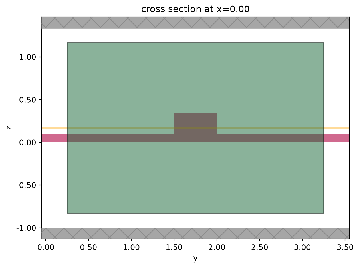
Charge scene#
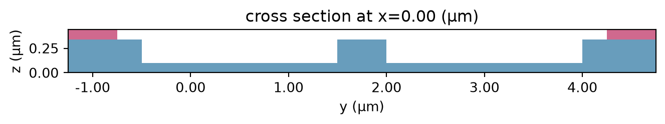
Now let’s put these structures together and check that it all looks good.
[10]:
scene_charge = td.Scene(
    structures=pin_wg + [contact_p, contact_n],
    medium=sio2,
)

scene_charge.plot(x=0)

plt.tight_layout()
plt.show()
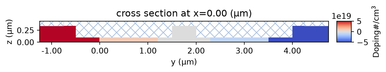
Let’s also inspect the doping profiles and make sure it is what we were expecting.
[11]:
scene_charge.plot_structures_property(x=0, property="doping")
plt.show()
Boundary conditions#
Since we’re interested in the response of the system for different applied voltages, we’ll need to solve the charge problem at each of these voltages. In Charge this can readily be done since the VoltageBC can accept an array of voltages as source through DCVoltageSource. A parameter scan will be run and the returned data will have the provided voltage values as a separate dimension.
Let’s define forward bias values up to 1.2 V with a step of 0.1 V.
[12]:
# create BCs
voltages = list(np.arange(13) * 0.1)

bc_v1 = td.HeatChargeBoundarySpec(
    condition=td.VoltageBC(source=td.DCVoltageSource(voltage=voltages)),
    placement=td.StructureBoundary(structure=contact_p.name),
)

bc_v2 = td.HeatChargeBoundarySpec(
    condition=td.VoltageBC(source=td.DCVoltageSource(voltage=0)),
    placement=td.StructureBoundary(structure=contact_n.name),
)

boundary_conditions = [bc_v1, bc_v2]
Charge monitors#
Since we’re interested in obtaining the free carrier distribution we’ll add a SteadyFreeCarrierMonitor to our Charge simulation. Note that the below monitor has been defined in the \(x=0\) plane.
[13]:
charge_mnt = td.SteadyFreeCarrierMonitor(
    center=(0, 0, 0),
    size=(0, effective_inf, effective_inf),
    name="charge_mnt",
    unstructured=True,
)
Charge simulation object#
When running Charge, we need to define the type of Charge simulation and some convergence settings. In the current case we set an relative tolerance of \(10^{-5}\) and an absolute tolerance of \(5\cdot 10^{10}\). The absolute tolerance may seem big though one should notice we have variables (electrons/holes) that take on values many orders of magnitude larger than the tolerance (\(\approx 10^{20}\)).
In the current case, we are going to run an isothermal DC case which we can define with IsothermalSteadyChargeDCAnalysis. In DC mode we can set the parameter convergence_dv which tells the solver to limit the size of the sweep, i.e., if we need to solve for a bias of 0 and 0.5 and we set convergence_dv=0.1, it will force the solver to go between 0 and 0.5 at intervals of 0.1.
We’ll also use a DistanceUnstructuredGrid with fine resolution around interfaces, and coarser resolution in bulk.
[14]:
convergence_settings = td.ChargeToleranceSpec()

analysis_type = td.IsothermalSteadyChargeDCAnalysis(
    temperature=300, tolerance_settings=convergence_settings, convergence_dv=0.1
)

res = 0.005  # resolution around interfaces in micron
mesh = td.DistanceUnstructuredGrid(
    dl_interface=res,
    dl_bulk=res * 10,
    distance_interface=res * 2,
    distance_bulk=res * 10,
    relative_min_dl=0.0,
)
We now have all the required elements to define a Charge simulation object. Note that the simulation has 0 size in the \(x\) direction. With this, we’ll make sure that the simulation is 2D even if the structures themselves are not.
[15]:
charge_sim = td.HeatChargeSimulation(
    monitors=[charge_mnt],
    analysis_spec=analysis_type,
    center=(0, wg_spacing / 2, (h_side + h_contact) / 2),
    size=(0, 2 * x_total + 0.1, h_side + h_contact + 0.1),
    structures=scene_charge.structures,
    medium=scene_charge.medium,
    boundary_spec=boundary_conditions,
    grid_spec=mesh,
)
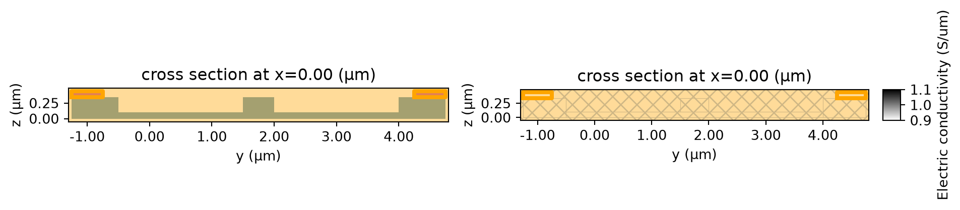
We can also plot here the simulation and some properties. In the properties plot, as well as the conductivity (which is invisible since the only conducting structures are the BC auxiliary ones) we can see the boundary conditions in blue and orange.
[16]:
# plot simulation
fig, ax = plt.subplots(1, 2, figsize=(10, 15))
charge_sim.plot(x=0, ax=ax[0])
charge_sim.plot_property(x=0, property="electric_conductivity", ax=ax[1])
plt.tight_layout()
plt.show()
[17]:
charge_data = web.run(charge_sim, task_name="mzi_pin", path="charge_mzi_pin.hdf5")
08:12:42 UTC Created task 'mzi_pin_mesh' with resource_id
             'vom-c609de59-5664-4a73-8c02-fa990805767f' and task_type
             'VOLUME_MESH'.
             Tidy3D's VolumeMesher solver is currently in the beta stage. Cost
             of VolumeMesher simulations is subject to change in the future.
08:12:44 UTC Estimated FlexCredit cost: 0.025. Use 'web.real_cost(task_id)' to
             get the billed FlexCredit cost after a simulation run.
08:12:45 UTC status = queued
             To cancel the simulation, use 'web.abort(task_id)' or
             'web.delete(task_id)' or abort/delete the task in the web UI.
             Terminating the Python script will not stop the job running on the
             cloud.
08:12:57 UTC starting up solver
running solver
08:13:01 UTC status = success
             Created task 'mzi_pin_solve' with resource_id
             'hec-78202987-c1a7-4e83-a96a-f134dfbab39f' and task_type
             'HEAT_CHARGE'.
             Tidy3D's HeatCharge solver is currently in the beta stage. Cost of
             HeatCharge simulations is subject to change in the future.
08:13:02 UTC Estimated typical FlexCredit cost: 0.025. For charge simulations,
             the billed cost depends on the number of solver iterations required
             for convergence.
             Maximum FlexCredit cost: 0.229. This assumes the charge solver
             reaches its configured iteration limits for all applied biases. Use
             'web.real_cost(task_id)' to get the billed FlexCredit cost after a
             simulation run.
08:13:06 UTC status = queued
             To cancel the simulation, use 'web.abort(task_id)' or
             'web.delete(task_id)' or abort/delete the task in the web UI.
             Terminating the Python script will not stop the job running on the
             cloud.
08:13:16 UTC status = preprocess
08:13:25 UTC starting up solver
running solver
08:13:27 UTC status = success
08:13:28 UTC Loading results from charge_mzi_pin.hdf5
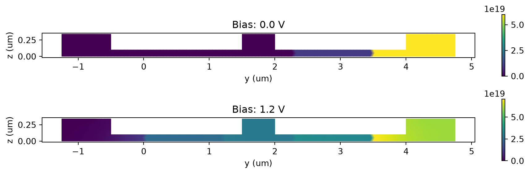
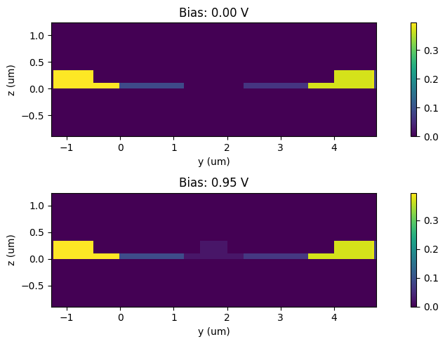
Carrier Distribution#
Let’s visualize the electron distributions for zero and 1.2 V biases.
[18]:
_, ax = plt.subplots(2, 1, figsize=(10, 3))

for ind, volt in enumerate([voltages[0], voltages[-1]]):
    charge_data["charge_mnt"].electrons.sel(x=0, voltage=volt).plot(ax=ax[ind], grid=False)
    ax[ind].set_title(f"Bias: {volt:1.1f} V")
    ax[ind].set_xlabel("y (um)")
    ax[ind].set_ylabel("z (um)")

plt.tight_layout()
plt.show()
Optic Simulations#
Having obtained free carrier solutions in the modulator cross section we can now turn to setting up optic simulation that will use these results.
We will use empiric relationships presented in M. Nedeljkovic, R. Soref and G. Z. Mashanovich, “Free-Carrier Electrorefraction and Electroabsorption Modulation Predictions for Silicon Over the 1–14- μm Infrared Wavelength Range,” IEEE Photonics Journal, vol. 3, no. 6, pp. 1171-1180, Dec. 2011, that state that changes in \(n\) and \(k\) of Si can be described by formulas
where \(\Delta N_e\) and \(\Delta N_h\) are electron and hole densities, and parameters have the following values for wavelength of 1.55 \(\mu\)m:
\(\lambda\) |
\(\frac{dn}{dN_e}\) |
\(\alpha\) |
\(\frac{dn}{dN_h}\) |
\(\beta\) |
\(\frac{dk}{dN_e}\) |
\(\gamma\) |
\(\frac{dk}{dN_h}\) |
\(\delta\) |
|---|---|---|---|---|---|---|---|---|
\(1.55\) |
\(5.40 \times 10^{-22}\) |
\(1.011\) |
\(1.53 \times 10^{-18}\) |
\(0.838\) |
\(8.88 \times 10^{-21}\) |
\(1.167\) |
\(5.84 \times 10^{-20}\) |
\(1.109\) |
[19]:
ne_coeff = -5.4e-22
ne_pow = 1.011

nh_coeff = -1.53e-18
nh_pow = 0.838

k_factor = wvl_um * 1e-4 / 4 / np.pi  # factor for conversion from absorption coefficient into k

ke_coeff = k_factor * 8.88e-21
ke_pow = 1.167

kh_coeff = k_factor * 5.84e-20
kh_pow = 1.109
Given the nonlinear character of these dependencies we will incorporate them as sampled function on a rectangular grid formed by electron and hole density values. Specifically, we will sample the given \(n\) and \(k\) dependencies in the electron and hole density ranges up to \(10^{20}\) 1/\(\text{cm}^3\).
[20]:
max_electron_exp = np.ceil(
    np.log10(charge_data["charge_mnt"].electrons.sel(x=0, y=2, z=0, method="nearest").values.max())
)
max_holes_exp = np.ceil(
    np.log10(charge_data["charge_mnt"].holes.sel(x=0, y=2, z=0, method="nearest").values.max())
)

print(f"Max electron density exponent: {max_electron_exp:.0f}")
print(f"Max hole density exponent: {max_holes_exp:.0f}")
Max electron density exponent: 20
Max hole density exponent: 20
[21]:
Ne_range = np.concatenate(([0], np.logspace(15, max_electron_exp, 20)))
Nh_range = np.concatenate(([0], np.logspace(15, max_holes_exp, 21)))

Ne_mesh, Nh_mesh = np.meshgrid(Ne_range, Nh_range, indexing="ij")

dn_mesh = ne_coeff * Ne_mesh**ne_pow + nh_coeff * Nh_mesh**nh_pow
dk_mesh = ke_coeff * Ne_mesh**ke_pow + kh_coeff * Nh_mesh**kh_pow
Now we convert sampled values of \(n\) and \(k\) into permittivity \(\varepsilon\) and conductivity \(\sigma\) values, and assemble a non-dispersive medium with perturbations (PerturbationMedium).
[22]:
dn_data = td.ChargeDataArray(dn_mesh, coords=dict(n=Ne_range, p=Nh_range))
dk_data = td.ChargeDataArray(dk_mesh, coords=dict(n=Ne_range, p=Nh_range))

n_si_charge = td.CustomChargePerturbation(perturbation_values=dn_data)
k_si_charge = td.CustomChargePerturbation(perturbation_values=dk_data)

n_si_perturbation = td.ParameterPerturbation(
    charge=n_si_charge,
)

k_si_perturbation = td.ParameterPerturbation(
    charge=k_si_charge,
)

si_perturb = td.PerturbationMedium.from_unperturbed(
    medium=si_non_perturb,
    perturbation_spec=td.IndexPerturbation(
        delta_n=n_si_perturbation,
        delta_k=k_si_perturbation,
        freq=freq0,
    ),
)
Circuits Structures#
For generating the entire circuit we use helper functions for creating a single waveguide and a waveguide y-junction (see tutorials Defining common integrated photonic components and Waveguide Y junction).
[23]:
def make_y_junction(
    x0,
    y0,
    z0,
    wg_thickness,
    wg_spacing,
    wg_length_in,
    wg_length_out,
    bend_length,
    direction,
    medium,
    sidewall_angle=0,
):

    w1, w2, w3, w4, w5 = 0.5, 0.5, 0.6, 0.7, 0.9
    w6, w7, w8, w9, w10 = 1.26, 1.4, 1.4, 1.4, 1.4
    w11, w12, w13 = 1.31, 1.2, 1.2

    l_junction = 2
    if wg_length_in < l_junction:
        raise ValueError(f"'wg_length_in' cannot be less than {l_junction}.")

    slab_bounds = (z0, z0 + wg_thickness)
    h_bend = (wg_spacing - w13 + w1) / 2

    x1 = x0 - direction * wg_length_out
    x2 = x1 - direction * bend_length
    x3 = x2 - direction * l_junction
    x4 = x2 - direction * wg_length_in

    y_out = y0 + wg_spacing / 2
    yb = y0 + w13 / 2 - w1 / 2

    bend_dir = (direction, 0)

    # input straight
    wg_in = pf.Path(origin=(x4, y0), width=w1).segment(endpoint=(x3, y0))

    # junction taper
    x_j = np.linspace(x3, x2, 13)
    w_j = np.array([w1, w2, w3, w4, w5, w6, w7, w8, w9, w10, w11, w12, w13])
    x_poly = np.concatenate((x_j, x_j[::-1]))
    y_poly = y0 + np.concatenate((w_j / 2, -w_j[::-1] / 2))
    junction = pf.Polygon(list(zip(x_poly, y_poly)))

    # bends
    bend_up = pf.Path(origin=(x2, yb), width=w1).s_bend(
        (direction * bend_length, h_bend), direction=bend_dir, relative=True
    )
    bend_down = pf.Path(origin=(x2, y0 - (yb - y0)), width=w1).s_bend(
        (direction * bend_length, -h_bend), direction=bend_dir, relative=True
    )

    # output straights
    straight_up = pf.Path(origin=(x1, y_out), width=w1).segment(endpoint=(x0, y_out))
    straight_down = pf.Path(origin=(x1, y0 - (y_out - y0)), width=w1).segment(
        endpoint=(x0, y0 - (y_out - y0))
    )

    polygons = pf.boolean(
        [wg_in, junction, bend_up, bend_down, straight_up, straight_down],
        [],
        "+",
    )
    assert len(polygons) == 1, f"Expected 1 polygon, got {len(polygons)}"
    polygon = polygons[0]
    assert len(polygon.holes) == 0

    geometry = td.PolySlab(
        vertices=polygon.vertices,
        axis=2,
        slab_bounds=slab_bounds,
        sidewall_angle=sidewall_angle,
    )
    return td.Structure(geometry=geometry, medium=medium)
Additionally, we create convenience functions to create a rib waveguide and a strip-to-rib taper.
[24]:
def make_strip_rib_taper(
    x0,
    y0,
    z0,
    x1,
    y1,
    core_width,
    slab_width,
    core_thickness,
    slab_thickness,
    medium,
    sidewall_angle=0,
):
    """
    This function defines a linear waveguide taper and returns the tidy3d structure of it.

    Parameters
    ----------
    x0: x coordinate of the waveguide starting position (um)
    y0: y coordinate of the waveguide starting position (um)
    z0: z coordinate of the waveguide bottom surface (um)
    x1: x coordinate of the waveguide end position (um)
    y1: y coordinate of the waveguide end position (um)
    core_width: width of the waveguide core (um)
    slab_width: width of the slab (um)
    core_thickness: thickness of the waveguide core (um)
    slab_thickness: thickness of the slab (um)
    medium: medium of the waveguide
    sidewall_angle: side wall angle of the waveguide (rad)
    """

    # core
    core = make_waveguide(
        x0=x0,
        y0=y0,
        z0=z0,
        x1=x1,
        y1=y1,
        wg_width_0=core_width,
        wg_width_1=core_width,
        wg_thickness=core_thickness,
        medium=medium,
        sidewall_angle=sidewall_angle,
    )

    # slab
    slab = make_waveguide(
        x0=x0,
        y0=y0,
        z0=z0,
        x1=x1,
        y1=y1,
        wg_width_0=core_width,
        wg_width_1=slab_width,
        wg_thickness=slab_thickness,
        medium=medium,
        sidewall_angle=sidewall_angle,
    )

    return [core, slab]
Now we need to create necessary components. Note that we use the medium with perturbation models only for the modulator section (pin_wg) as the rest of the structures are assumed to be undoped. Note that we’re recreating the waveguide in the PIN region so that we can use the perturbed silicon.
[25]:
# input coupler
coupler_in = make_y_junction(
    x0=-mzi_length / 2,
    y0=0,
    z0=0,
    wg_thickness=h_core,
    wg_spacing=wg_spacing,
    wg_length_in=y_length_in,
    wg_length_out=y_length_out,
    bend_length=y_length_bend,
    direction=1,
    medium=si_non_perturb,
    sidewall_angle=0,
)

# output coupler
coupler_out = make_y_junction(
    x0=mzi_length / 2,
    y0=0,
    z0=0,
    wg_thickness=h_core,
    wg_spacing=wg_spacing,
    wg_length_in=y_length_in,
    wg_length_out=y_length_out,
    bend_length=y_length_bend,
    direction=-1,
    medium=si_non_perturb,
    sidewall_angle=0,
)

# bottom arm
bot_arm = make_waveguide(
    x0=-mzi_length / 2,
    y0=-wg_spacing / 2,
    z0=0,
    x1=mzi_length / 2,
    y1=-wg_spacing / 2,
    wg_width_0=w_core,
    wg_width_1=w_core,
    wg_thickness=h_core,
    medium=si_non_perturb,
    sidewall_angle=0,
)

# top arm: taper in
taper_in = make_strip_rib_taper(
    x0=-mzi_length / 2,
    y0=wg_spacing / 2,
    z0=0,
    x1=-pin_length / 2,
    y1=wg_spacing / 2,
    core_width=w_core,
    slab_width=2 * x_side,
    core_thickness=h_core,
    slab_thickness=h_slab,
    medium=si_non_perturb,
    sidewall_angle=0,
)

# top arm: PIN region
pin_wg = make_rib_waveguide(
    x0=-pin_length / 2,
    y0=wg_spacing / 2,
    z0=0,
    x1=pin_length / 2,
    y1=wg_spacing / 2,
    core_width=w_core,
    slab_width=2 * x_total,
    side_width=x_total - x_side,
    core_thickness=h_core,
    slab_thickness=h_slab,
    side_thickness=h_side,
    medium=si_perturb,
    sidewall_angle=0,
)


# top arm: taper out
taper_out = make_strip_rib_taper(
    x0=mzi_length / 2,
    y0=wg_spacing / 2,
    z0=0,
    x1=pin_length / 2,
    y1=wg_spacing / 2,
    core_width=w_core,
    slab_width=2 * x_side,
    core_thickness=h_core,
    slab_thickness=h_slab,
    medium=si_non_perturb,
    sidewall_angle=0,
)
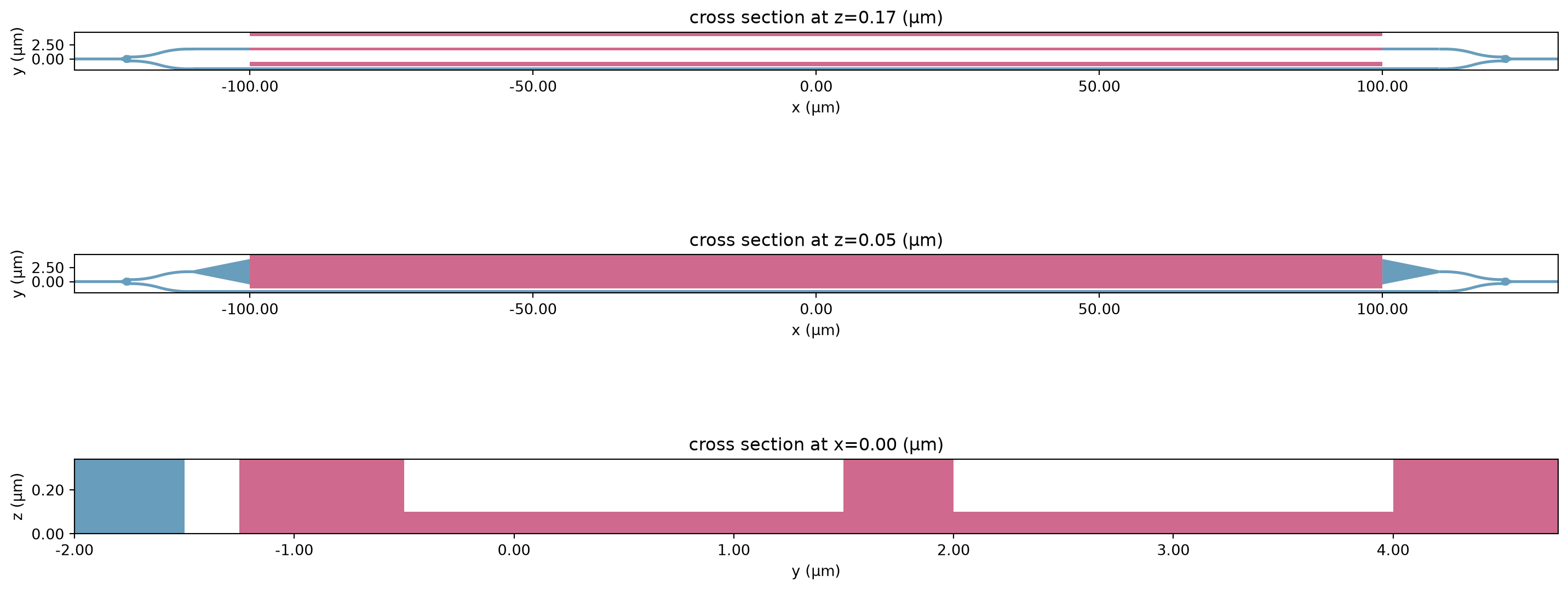
Before proceeding further into creating an optic simulation, we can combine created structures into a Scene object for visualization purposes.
[26]:
scene = td.Scene(
    structures=[coupler_in, coupler_out, bot_arm] + taper_in + pin_wg + taper_out,
    medium=sio2,
)

_, ax = plt.subplots(3, 1, figsize=(15, 7))
scene.plot(z=z_core, ax=ax[0])
scene.plot(z=z_slab, ax=ax[1])
scene.plot(x=0, ax=ax[2])

plt.tight_layout()
plt.show()
Optic Sources and Monitors#
Having inspected the geometry we now continue to define other components of an optic simulation. First, we define several auxiliary variables corresponding to: - SiO2 buffer around the circuit, - reduction of simulation in x direction, - location and size of source injection and monitor ports, - width of the injected pulse, and - frequencies at which to measure output signals.
[27]:
buffer = 1
dx = 6

port_x = mzi_length / 2 + splitter_length - dx - 1
port_y = 0
port_z = z_core

port_size = (0, 3, 2)

fwidth = freq0 / 5
freqs = np.linspace(freq0 - fwidth / 10, freq0 + fwidth / 10, 201)
wvls = td.C_0 / freqs
The propagation of EM pulse in the circuit is triggered by a ModeSource.
[28]:
src = td.ModeSource(
    center=(-port_x - 0.5, port_y, port_z),
    size=port_size,
    direction="+",
    mode_index=0,
    source_time=td.GaussianPulse(freq0=freq0, fwidth=fwidth),
)
We will measure mode decompositions in the input port and two output ports. Additionally, we will sample field distribution on the horizontal plane passing through the circuit’s center.
[29]:
mnt_in = td.ModeMonitor(
    center=(-port_x, port_y, port_z),
    size=port_size,
    freqs=freqs,
    mode_spec=td.ModeSpec(num_modes=3),
    name="in",
)
mnt_out = td.ModeMonitor(
    center=(port_x, port_y, port_z),
    size=port_size,
    freqs=freqs,
    mode_spec=td.ModeSpec(num_modes=3),
    name="out",
)
mnt_field = td.FieldMonitor(
    center=(0, 0, z_core), size=(effective_inf, effective_inf, 0), freqs=[freq0], name="field"
)
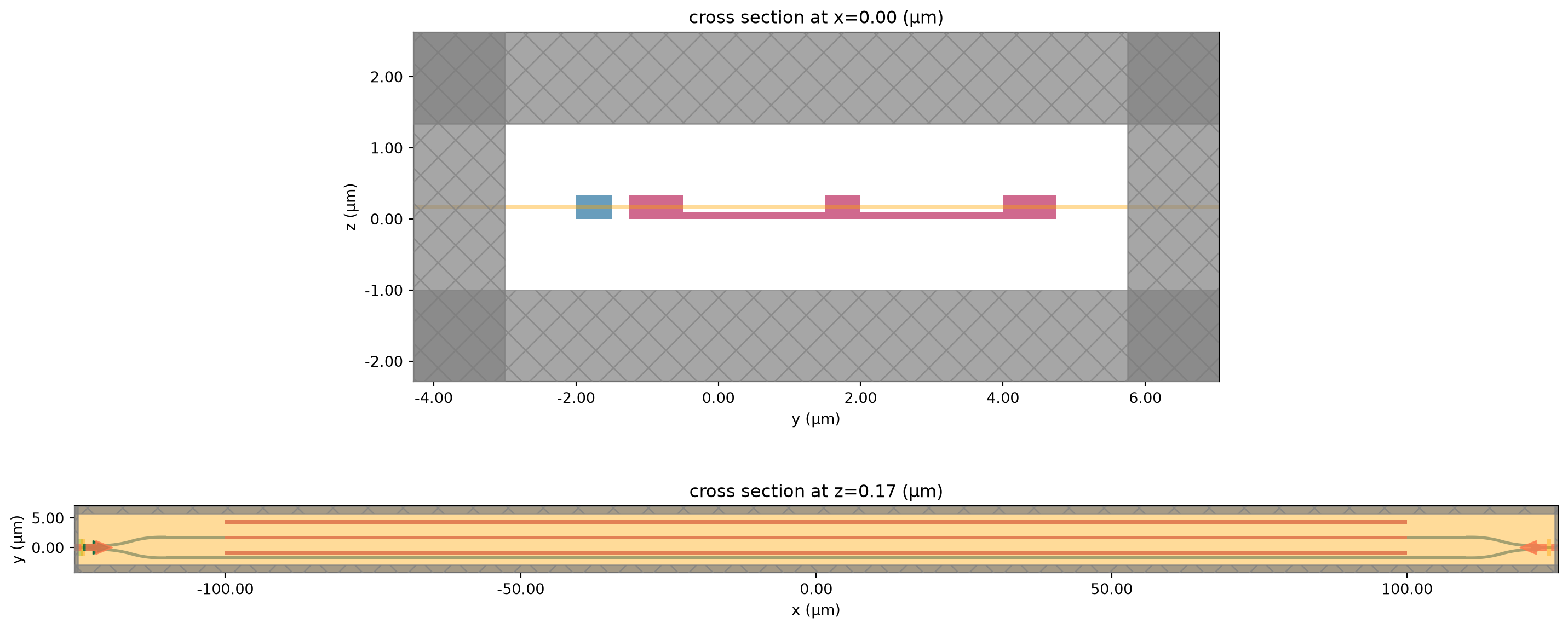
Simulation Assembly#
[30]:
sim_size = (scene.size[0] - 2 * dx, scene.size[1] + 2 * buffer, scene.size[2] + 2 * buffer)

sim = td.Simulation.from_scene(
    scene,
    center=scene.center,
    size=sim_size,
    sources=[src],
    monitors=[mnt_in, mnt_out, mnt_field],
    run_time=6e-11,
)
Let us perform another visual inspection to ensure the right placement of monitors and sources.
[31]:
_, ax = plt.subplots(2, 1, figsize=(15, 7))
sim.plot(x=sim.center[0], ax=ax[0])
sim.plot(z=sim.center[2], ax=ax[1])

plt.tight_layout()
plt.show()
This can also be done using a three dimensional plotting functionality.
[32]:
sim.plot_3d(width=800, height=600)
Applying Carrier Distributions#
At this point we have created an optic simulation that contains materials with charge perturbation models, however no electron and hole distributions have been provided to it. That is, when we submit such a simulation for solving, all mediums with perturbation models will be considered as regular materials with no perturbations applied. In our case, this corresponds to the case of undoped materials.
To obtain simulations in which perturbation models are sampled against provided carrier densities one can use a convenience method perturbed_mediums_copy().
[33]:
def apply_charge(charge_data):
    perturbed_sims = []
    for n, v in enumerate(charge_data["charge_mnt"].electrons.values.voltage.data):
        e_data = charge_data["charge_mnt"].electrons.sel(voltage=v)
        h_data = charge_data["charge_mnt"].holes.sel(voltage=v)
        perturbed_sims.append(
            sim.perturbed_mediums_copy(
                electron_density=e_data,
                hole_density=h_data,
            )
        )
    return perturbed_sims


perturbed_sims = apply_charge(charge_data)
The difference in the permittivity values in the modulator cross-section compared to the undoped case can be visualized as follows.
[34]:
_, ax = plt.subplots(2, 1, figsize=(10, 5))

sampling_region = td.Box(center=(0, wg_spacing / 2, port_z), size=(0, 6, 2))
eps_undoped = sim.epsilon(box=sampling_region).isel(x=0, drop=True)

for ax_ind, ind in enumerate([5, 10]):
    eps_doped = perturbed_sims[ind].epsilon(box=sampling_region).isel(x=0, drop=True)
    eps_doped = eps_doped.interp(y=eps_undoped.y, z=eps_undoped.z)
    eps_diff = np.abs(np.real(eps_doped - eps_undoped))
    eps_diff.plot(x="y", ax=ax[ax_ind])

    ax[ax_ind].set_aspect("equal")
    ax[ax_ind].set_title(f"Bias: {voltages[ind]:1.1f} V")
    ax[ax_ind].set_xlabel("y (um)")
    ax[ax_ind].set_ylabel("z (um)")

plt.tight_layout()
plt.show()
Waveguide Mode Analysis#
Before proceeding to full-wave simulations one can investigate the influence of applied voltage on the propagation index of waveguide modes in the modulator.
[35]:
from tidy3d.plugins.mode import ModeSolver
Let us define a plane for which waveguide modes will be calculated.
[36]:
mode_plane = td.Box(center=(0, wg_spacing / 2, port_z), size=port_size)

# visualize
ax = sim.plot(x=mode_plane.center[0])
mode_plane.plot(x=mode_plane.center[0], ax=ax, alpha=0.5)
plt.show()
Create a mode solver specification for each carrier distribution. We will consider only the first mode at 11 different frequencies. Also, given that the anticipated changes are small, double precision is turned on for mode solving.
[37]:
mode_solvers = {}
for n, psim in enumerate(perturbed_sims):
    ms = ModeSolver(
        simulation=psim,
        plane=mode_plane,
        freqs=np.linspace(freqs[0], freqs[-1], 11),
        mode_spec=td.ModeSpec(num_modes=1, precision="double"),
    )
    mode_solvers[f"v={voltages[n]}"] = ms
Perform calculation on our servers. Note that since the associated simulation objects contain custom medium data, they are automatically reduced to the mode solver plane for optimizing uploading/downloading data. Setting reduce_simulation=True will silence the associated warning.
[38]:
batch = web.Batch(simulations=mode_solvers, reduce_simulation=True)
ms_data = batch.run()
08:14:08 UTC Started working on Batch containing 13 tasks.
08:14:20 UTC Maximum FlexCredit cost: 0.064 for the whole batch.
             Use 'Batch.real_cost()' to get the billed FlexCredit cost after
             completion.
08:14:39 UTC Batch complete.
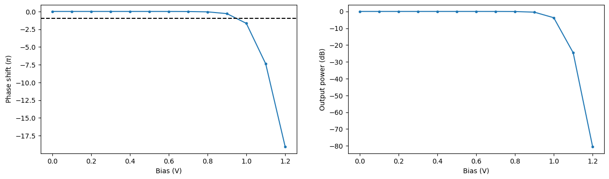
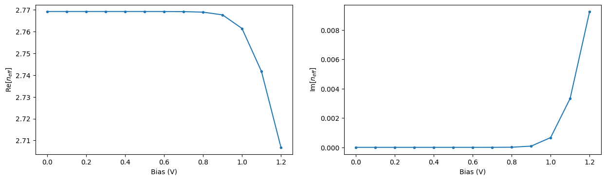
Let us extract the effective propagation index for the central frequency and visualize its dependence on applied voltage. As expected, increasing the applied voltage results in a more pronounced change in the propagation index and, at the same time, in larger losses in the waveguide.
[39]:
n_eff_freq0 = [md.n_complex.sel(f=freq0, mode_index=0).values for _, md in ms_data.items()]

_, ax = plt.subplots(1, 2, figsize=(15, 4))
ax[0].plot(voltages, np.real(n_eff_freq0), ".-")

ax[0].set_xlabel("Bias (V)")
ax[0].set_ylabel("Re[$n_{eff}$]")

ax[1].plot(voltages, np.imag(n_eff_freq0), ".-")

ax[1].set_xlabel("Bias (V)")
ax[1].set_ylabel("Im[$n_{eff}$]")

plt.show()
Using the obtained propagation index values we can compute the associated phase change and loss over the PIN section of the modulator at the central wavelength of 1.55 um. From this information we can estimate the bias \(V_\pi\) required for a phase shift of \(\pi\) to be around 0.95 V. In Zhou Liang et al 2011 Chinese Phys. Lett. 28 074202 the value of 1.15 V was obtained for a similar experimental setup.
[40]:
phase_shift = 2 * np.pi / wvl_um * (np.real(n_eff_freq0) - np.real(n_eff_freq0[0])) * pin_length
intensity = np.exp(-4 * np.pi * np.imag(n_eff_freq0) * pin_length / wvl_um)

_, ax = plt.subplots(1, 2, figsize=(15, 4))
ax[0].plot(voltages, phase_shift / np.pi, ".-")
ax[0].axhline(y=-1, color="k", linestyle="--")

ax[0].set_xlabel("Bias (V)")
ax[0].set_ylabel(r"Phase shift ($\pi$)")

ax[1].plot(voltages, 10 * np.log10(intensity), ".-")

ax[1].set_xlabel("Bias (V)")
ax[1].set_ylabel("Output power (dB)")

plt.show()
Full-wave simulation of the circuit#
Note: the cost of running this section is over 15 FlexCredits.
While performing full-wave simulations is not the most cost effective approach for such a simple geometry, we still perform it here for zero and 1 V bias values for demonstration purposes. Alternatively, one could achieve the full-wave simulation accuracy by dividing the problem setup into smaller components and obtaining the S-matrix for each of them using Tidy3D’s ComponentModeler plugin. Here, we simply perform the simulation over the entire circuit.
For a clearer demonstration let us obtain free carrier distribution for the approximately found \(V_\pi\) of 0.95 V.
[41]:
bc_v1 = td.HeatChargeBoundarySpec(
    condition=td.VoltageBC(source=td.DCVoltageSource(voltage=[0, 0.95])),
    placement=td.StructureBoundary(structure=contact_p.name),
)

boundary_conditions = [bc_v1, bc_v2]

charge_sim_95 = charge_sim.updated_copy(boundary_spec=boundary_conditions)

charge_data_95 = web.run(charge_sim_95, task_name="mzi_pin_Vpi", path="charge_mzi_pin_Vpi.hdf5")
08:15:34 UTC Created task 'mzi_pin_Vpi_mesh' with resource_id
             'vom-e8967922-abbd-4227-8bed-f0c90070c1b9' and task_type
             'VOLUME_MESH'.
             Tidy3D's VolumeMesher solver is currently in the beta stage. Cost
             of VolumeMesher simulations is subject to change in the future.
08:15:35 UTC Estimated FlexCredit cost: 0.025. Use 'web.real_cost(task_id)' to
             get the billed FlexCredit cost after a simulation run.
08:15:36 UTC status = queued
             To cancel the simulation, use 'web.abort(task_id)' or
             'web.delete(task_id)' or abort/delete the task in the web UI.
             Terminating the Python script will not stop the job running on the
             cloud.
08:16:02 UTC starting up solver
running solver
08:16:03 UTC status = success
             Created task 'mzi_pin_Vpi_solve' with resource_id
             'hec-56b7f346-5451-49c6-a514-0032813409d8' and task_type
             'HEAT_CHARGE'.
             Tidy3D's HeatCharge solver is currently in the beta stage. Cost of
             HeatCharge simulations is subject to change in the future.
08:16:04 UTC Estimated typical FlexCredit cost: 0.025. For charge simulations,
             the billed cost depends on the number of solver iterations required
             for convergence.
             Maximum FlexCredit cost: 0.148. This assumes the charge solver
             reaches its configured iteration limits for all applied biases. Use
             'web.real_cost(task_id)' to get the billed FlexCredit cost after a
             simulation run.
08:16:06 UTC status = queued
             To cancel the simulation, use 'web.abort(task_id)' or
             'web.delete(task_id)' or abort/delete the task in the web UI.
             Terminating the Python script will not stop the job running on the
             cloud.
08:16:15 UTC status = preprocess
08:16:27 UTC starting up solver
running solver
08:16:28 UTC status = success
08:16:29 UTC Loading results from charge_mzi_pin_Vpi.hdf5
[42]:
perturbed_sim_0_95V = apply_charge(charge_data_95)
[43]:
_, ax = plt.subplots(2, 1, figsize=(10, 5))

sampling_region = td.Box(center=(0, wg_spacing / 2, port_z), size=(0, 6, 2))
eps_undoped = sim.epsilon(box=sampling_region).isel(x=0, drop=True)

for ind in range(2):
    eps_doped = perturbed_sim_0_95V[ind].epsilon(box=sampling_region).isel(x=0, drop=True)
    eps_doped = eps_doped.interp(y=eps_undoped.y, z=eps_undoped.z)
    eps_diff = np.abs(np.real(eps_doped - eps_undoped))
    eps_diff.plot(x="y", ax=ax[ind])

    ax[ind].set_aspect("equal")
    ax[ind].set_title(f"Bias: {[0, 0.95][ind]:1.2f} V")
    ax[ind].set_xlabel("y (um)")
    ax[ind].set_ylabel("z (um)")

plt.tight_layout()
plt.show()

For convenience, we use Batch functionality to submit two simulation for solving in parallel.
[44]:
batch = web.Batch(
    simulations={"Bias: 0 V": perturbed_sims[0], "Bias: 0.95 V": perturbed_sim_0_95V[-1]}
)
batch_data = batch.run()
08:16:45 UTC Started working on Batch containing 2 tasks.
08:16:48 UTC Maximum FlexCredit cost: 27.215 for the whole batch.
             Use 'Batch.real_cost()' to get the billed FlexCredit cost after
             completion.
08:27:31 UTC Batch complete.
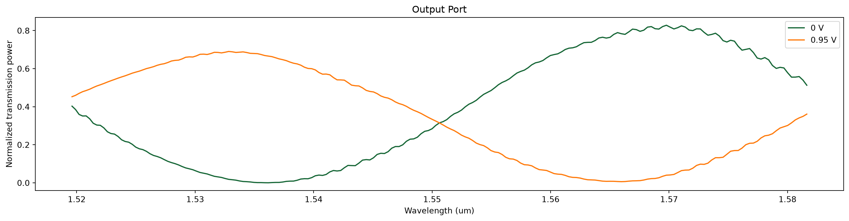
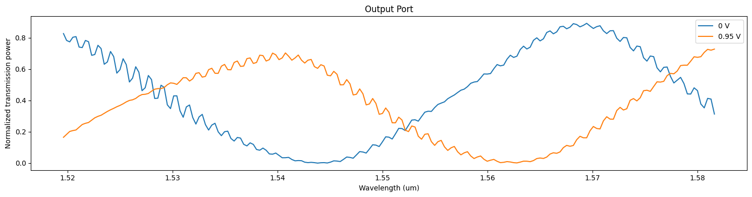
Let us first visualize the field distribution across the whole circuit. Comparing the two simulations, one can qualitatively observe two effects:
power in the output waveguide is drastically changed as bias value of 0.95 V is close to \(V_\pi\),
the signal strength visibly decreases along the PIN section of the modulator in the case of 0.95 V bias value due to losses associated with the increased concentration of free carriers.
Note that unequal aspect ratio is used for plotting.
[45]:
_, ax = plt.subplots(2, 1, figsize=(10, 10))

for ind, (key, data) in enumerate(batch_data.items()):
    batch_data[key].plot_field("field", "S", ax=ax[ind])
    ax[ind].set_title(key)
    ax[ind].set_aspect("auto")

plt.tight_layout()
plt.show()
A more quantitative visualization of data can be obtained from the output ModeMonitor results.
[46]:
_, ax = plt.subplots(1, 1, figsize=(15, 4))
for ind, (key, data) in enumerate(batch_data.items()):
    ax.plot(wvls, batch_data[key]["out"].amps.sel(direction="+", mode_index=0).abs ** 2)

ax.set_title("Output Port")
ax.set_xlabel("Wavelength (um)")
ax.set_ylabel("Normalized transmission power")
ax.legend(["0 V", "0.95 V"])

plt.tight_layout()
plt.show()