

Mode overlap integral between a waveguide mode and a Gaussian mode#
The evaluation of the overlap integral quantifies the level of matching between two optical field distributions. It is particularly useful, for example, in determining the coupling efficiency to the desired waveguide mode when connecting an optical fiber to an edge coupler.
Tidy3D facilitates the analytical computation of field distributions for different beam types including Gaussian beam, astigmatic Gaussian beam, and plane wave. This feature enables swift calculation of mode overlap integral with another mode, likely determined through a mode solver analysis.
This notebook presents the optimization of coupling efficiency between a single-mode fiber (represented by a Gaussian mode field) and a silicon edge coupler. The focus is to highlight the usage of built-in functions for the analytical computation of the Gaussian beam profile and overlap integral calculation.
[1]:
from __future__ import annotations

import matplotlib.pyplot as plt
import numpy as np
import tidy3d as td
import tidy3d.web as web
Generate the Gaussian Beam Profile#
The Gaussian beam is analytically defined by
where the beam parameters are defined as follows:
Beam radius:
with \(w_0\) as the waist radius and \(z_0\) as the waist distance.
Rayleigh range:
Radius of curvature:
Gouy phase:
A Gaussian beam field profile can be generated directly through GaussianBeamProfile. Similarly, an astigmatic Gaussian beam profile can be generated through AstigmaticGaussianBeamProfile and a plane wave profile can be generated through PlaneWaveBeamProfile.
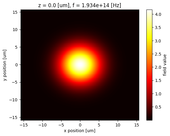
In this notebook, we want to optimize the coupling between an SMF-28 and a 220 nm SOI edge coupler by adjusting the waveguide width at the end of the edge coupler. This requires us to perform mode analysis on the waveguide cross section with varying widths and then perform mode overlap integral with the fiber mode. For SMF-28, the mode field diameter at 1550 nm is about 10.5 μm. Therefore, we can represent the mode field with a Gaussian beam with a waist_radius of 5.25 μm.
[2]:
lda0 = 1.55  # wavelength of interest
freq0 = td.C_0 / lda0  # frequency of interest
r_beam = 5.25  # beam radius
size = 40  # plane size for the beam profile
In order to accurately capture the full profile of the Gaussian beam, it is imperative to ensure the plane size is sufficiently large, at least a few times larger than the beam size. The size argument also expects one of the values to be 0. The direction with a zero size is taken as the propagation axis. For example, if size=(size_x, size_y, 0), the Gaussian beam is propagating in the \(z\) direction. Additional arguments such as angle_theta and angle_phi can be specified if
the desired propagation direction is not parallel to one of the Cartesian axes, similar to defining a regular GaussianBeam source in FDTD.
Additionally, it’s necessary to align the polarization angle with the desired waveguide mode for effective coupling. In this particular scenario, the target is coupling to the fundamental TE mode that is polarized in the y-direction.
The resolution parameter is crucial as it defines the sampling resolution and it needs to be appropriately high to ensure precision.
[3]:
# generate a Gaussian beam
gaussian_beam = td.GaussianBeamProfile(
    waist_radius=r_beam,
    pol_angle=np.pi / 2,  # polarized in the y direction for coupling to the TE mode
    size=(size, size, 0),
    resolution=200,
    freqs=[freq0],
)
Once the beam is generated, we can visualize the field profile.
[4]:
gaussian_beam.field_data.Ey.abs.plot(cmap="hot", x="x", y="y")
plt.show()
Conducting Mode Analysis on the Waveguide#
We will proceed by performing a mode analysis on the waveguide structure at the end facet of the edge coupler. Our aim is to sweep a range of waveguide widths to identify the optimal value, one which would result in the highest coupling efficiency. To accomplish this, we first define a function make_mode_simulation. This function takes the waveguide width as an input parameter and returns a ModeSimulation instance, which we solve on the cloud through web.run.
[5]:
# materials used
si = td.material_library["cSi"]["Li1993_293K"]
sio2 = td.material_library["SiO2"]["Horiba"]

# thickness of the waveguide
h = 0.22


def make_mode_simulation(w):
    waveguide = td.Structure(geometry=td.Box(center=(0, 0, 0), size=(h, w, td.inf)), medium=si)

    mode_sim = td.ModeSimulation(
        center=(0, 0, 0),
        size=(size, size, 0),
        grid_spec=td.GridSpec.auto(min_steps_per_wvl=25, wavelength=lda0),
        structures=[waveguide],
        medium=sio2,
        symmetry=(1, -1, 0),  # symmetry for the fundamental TE mode
        plane=td.Box(center=(0, 0, 0), size=(size, size, 0)),
        mode_spec=td.ModeSpec(num_modes=1, target_neff=3.5),
        freqs=[freq0],
    )

    return mode_sim
We investigate the waveguide width from 100 to 200 nm in increment of 10 nm. All 11 mode simulations are passed together to web.run, which runs them in parallel. Each result is a ModeSimulationData, and we collect the underlying mode data from its modes attribute.
[6]:
w_list = np.linspace(0.1, 0.2, 11)
mode_sims = {f"w={w:.2f}": make_mode_simulation(w) for w in w_list}

mode_results = web.run(mode_sims)
mode_data = {key: result.modes for key, result in mode_results.items()}
22:23:15 UTC Started working on Batch containing 11 tasks.
22:23:24 UTC Maximum FlexCredit cost: 0.133 for the whole batch.
             Use 'Batch.real_cost()' to get the billed FlexCredit cost after
             completion.
22:28:06 UTC Batch complete.
Mode Overlap Integral#
After running the mode simulations, we are ready to perform the mode overlap integral (modal decomposition) between the waveguide mode and the Gaussian mode for each waveguide width. This can be achieved easily with the built-in outer_dot method, which implements
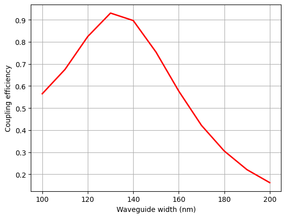
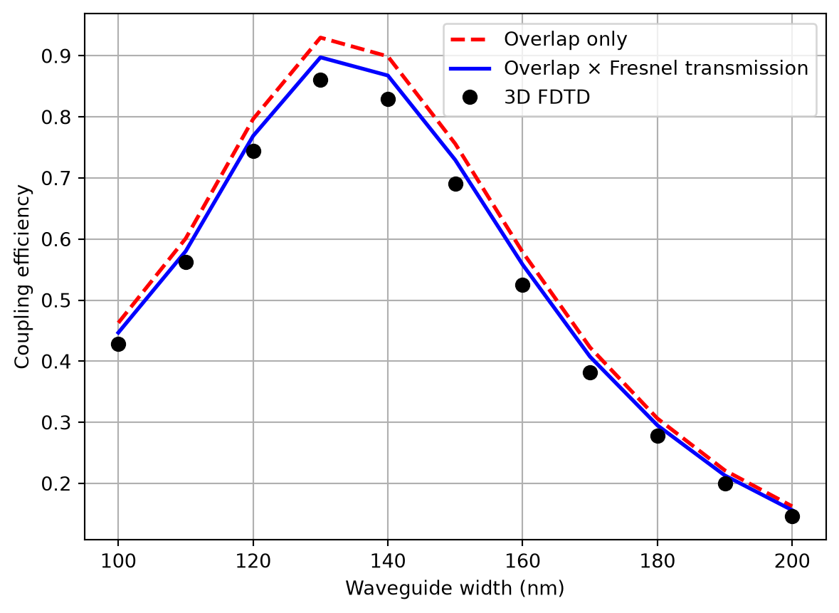
After the overlap integrals are calculated, we can plot the coupling efficiency as a function of the waveguide width to identify the optimal value. In this case, the optimal width is between 130 and 140 nm.
[7]:
overlap = [
    mode_data[f"w={w:.2f}"].outer_dot(gaussian_beam.field_data).values.squeeze() for w in w_list
]

plt.plot(1e3 * w_list, np.abs(overlap) ** 2, "r", linewidth=2)
plt.xlabel("Waveguide width (nm)")
plt.ylabel("Coupling efficiency")
plt.grid()
Accounting for Fresnel Reflection#
The overlap integral above measures how well the spatial profiles of the fiber and waveguide modes match, but it assumes both modes propagate in the same medium. What we actually inject at the chip facet is the beam that the fiber emits, which we model as a Gaussian beam propagating through the free space (\(n = 1\)) in front of the chip.
At the facet this beam enters the higher-index waveguide, so part of the power is reflected. We approximate the reflecting medium by the effective index \(n_{eff}\) of the waveguide mode returned by the mode solver, since it already accounts for how the field is distributed between the core and the cladding. The Fresnel amplitude reflection coefficient is then
so a fraction \(R = |r|^2\) of the power is reflected and only \(T = 1 - R\) is transmitted. The actual coupling efficiency is therefore the mode overlap multiplied by the Fresnel transmission \(T\).
[8]:
n_eff = np.array([mode_data[f"w={w:.2f}"].n_eff.values.squeeze() for w in w_list])

r_fresnel = (1 - n_eff) / (1 + n_eff)
T_fresnel = 1 - np.abs(r_fresnel) ** 2

overlap_efficiency = np.abs(overlap) ** 2
coupling_efficiency = overlap_efficiency * T_fresnel

plt.plot(1e3 * w_list, overlap_efficiency, "r--", linewidth=2, label="Overlap only")
plt.plot(
    1e3 * w_list, coupling_efficiency, "b", linewidth=2, label="Overlap × Fresnel transmission"
)
plt.xlabel("Waveguide width (nm)")
plt.ylabel("Coupling efficiency")
plt.legend()
plt.grid()
plt.show()
Validation with 3D FDTD#
To verify the semi-analytical coupling efficiency, we model the actual edge coupling process with a full 3D FDTD simulation for each waveguide width. A GaussianBeam source reproduces the beam emitted by the fiber and launches it through free space toward the chip facet, where the \(\text{SiO}_2\)-clad silicon waveguide begins. Since the semi-analytical overlap assumes the beam waist lies on the facet plane, we set waist_distance such that the waist is placed at the facet
(\(z=0\)) rather than at the source plane. A ModeMonitor placed inside the waveguide records the fundamental TE mode amplitude; the squared magnitude of its forward-propagating component is the coupling efficiency, which now includes both the modal overlap and the Fresnel reflection at the facet.
We define a helper function make_fdtd_sim that builds the simulation for a given waveguide width. The free-space region (\(z<0\)) is the space in front of the chip through which the fiber’s beam propagates, while the silicon core and its \(\text{SiO}_2\) cladding occupy \(z>0\).
[9]:
size_fdtd = size  # transverse domain taken from the mode plane size, so both use the same window
z_src, z_mon, z_min, z_max = -1.5, 3.0, -3.0, 5.0

# SiO2 cladding fills the chip side (z > 0); the silicon core sits inside it
cladding = td.Structure(
    geometry=td.Box(center=(0, 0, z_max), size=(td.inf, td.inf, 2 * z_max)),
    medium=sio2,
)


def make_fdtd_sim(w):
    core = td.Structure(
        geometry=td.Box(center=(0, 0, z_max), size=(h, w, 2 * z_max)),
        medium=si,
    )

    source = td.GaussianBeam(
        center=(0, 0, z_src),
        size=(td.inf, td.inf, 0),
        source_time=td.GaussianPulse(freq0=freq0, fwidth=freq0 / 10),
        direction="+",
        waist_radius=r_beam,
        waist_distance=z_src,  # negative value places the waist at the chip facet (z=0), matching the overlap model
        pol_angle=np.pi / 2,  # y-polarized for the TE mode
    )

    mode_monitor = td.ModeMonitor(
        center=(0, 0, z_mon),
        size=(size_fdtd, size_fdtd, 0),
        freqs=[freq0],
        mode_spec=td.ModeSpec(num_modes=1, target_neff=3.5),
        name="mode",
    )

    sim = td.Simulation(
        center=(0, 0, (z_min + z_max) / 2),
        size=(size_fdtd, size_fdtd, z_max - z_min),
        grid_spec=td.GridSpec.auto(min_steps_per_wvl=20, wavelength=lda0),
        structures=[cladding, core],
        sources=[source],
        monitors=[mode_monitor],
        run_time=2e-12,
        medium=td.Medium(permittivity=1),  # free space on the fiber side
        symmetry=(1, -1, 0),
        boundary_spec=td.BoundarySpec.all_sides(boundary=td.PML()),
    )

    return sim
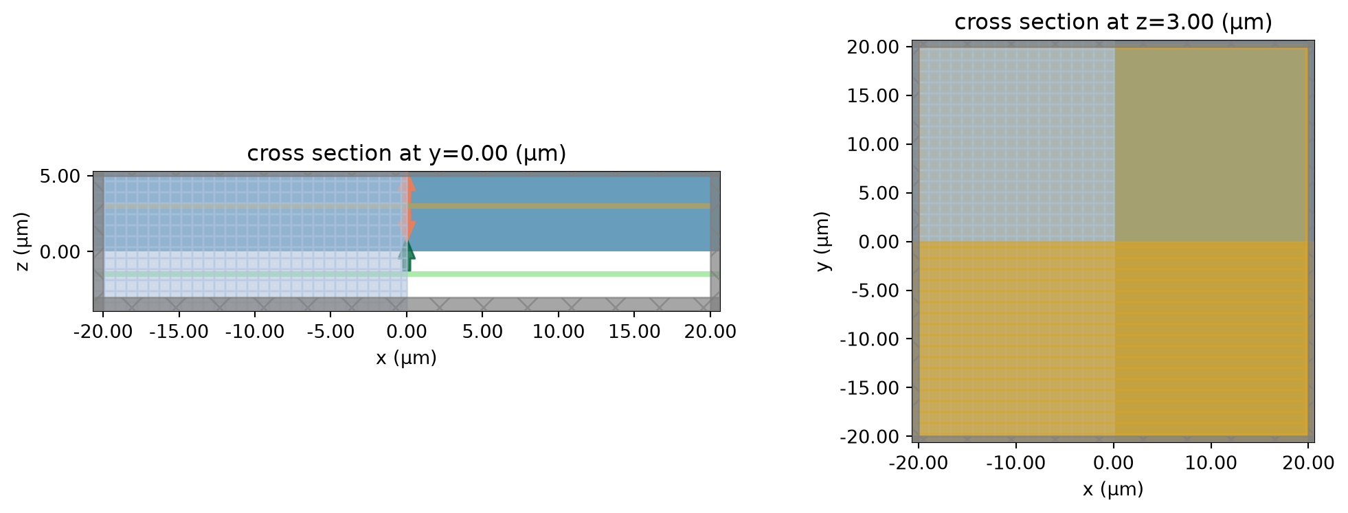
Before launching the batch, we visualize the simulation setup for the optimal width to confirm that the source, monitor, and geometry are placed correctly. The left panel shows the propagation plane with the free-space input region, the facet at \(z=0\), the source, and the mode monitor; the right panel shows the transverse plane at the monitor.
[10]:
sim_example = make_fdtd_sim(0.13)

fig, (ax1, ax2) = plt.subplots(1, 2, figsize=(11, 4))
sim_example.plot(y=0, ax=ax1)
sim_example.plot(z=z_mon, ax=ax2)
plt.tight_layout()
plt.show()
We pass all 11 simulations together to web.run, which runs them in parallel, then read the coupling efficiency from each mode monitor.
[11]:
fdtd_sims = {f"w={w:.2f}": make_fdtd_sim(w) for w in w_list}

fdtd_results = web.run(fdtd_sims)
22:28:15 UTC WARNING: Mode monitor 'mode' has a large number (5.84e+05) of grid
             points. This can lead to solver slow-down and increased cost.
             Consider making the size of the component smaller, as long as the
             modes of interest decay by the plane boundaries.
WARNING: Suppressed 1 WARNING message.
             WARNING: Mode monitor 'mode' has a large number (5.84e+05) of grid
             points. This can lead to solver slow-down and increased cost.
             Consider making the size of the component smaller, as long as the
             modes of interest decay by the plane boundaries.
             WARNING: Mode monitor 'mode' has a large number (5.84e+05) of grid
             points. This can lead to solver slow-down and increased cost.
             Consider making the size of the component smaller, as long as the
             modes of interest decay by the plane boundaries.
             WARNING: Mode monitor 'mode' has a large number (5.84e+05) of grid
             points. This can lead to solver slow-down and increased cost.
             Consider making the size of the component smaller, as long as the
             modes of interest decay by the plane boundaries.
             WARNING: Mode monitor 'mode' has a large number (5.84e+05) of grid
             points. This can lead to solver slow-down and increased cost.
             Consider making the size of the component smaller, as long as the
             modes of interest decay by the plane boundaries.
             WARNING: Mode monitor 'mode' has a large number (5.85e+05) of grid
             points. This can lead to solver slow-down and increased cost.
             Consider making the size of the component smaller, as long as the
             modes of interest decay by the plane boundaries.
             WARNING: Mode monitor 'mode' has a large number (5.85e+05) of grid
             points. This can lead to solver slow-down and increased cost.
             Consider making the size of the component smaller, as long as the
             modes of interest decay by the plane boundaries.
             WARNING: Mode monitor 'mode' has a large number (5.84e+05) of grid
             points. This can lead to solver slow-down and increased cost.
             Consider making the size of the component smaller, as long as the
             modes of interest decay by the plane boundaries.
             WARNING: Mode monitor 'mode' has a large number (5.85e+05) of grid
             points. This can lead to solver slow-down and increased cost.
             Consider making the size of the component smaller, as long as the
             modes of interest decay by the plane boundaries.
             WARNING: Mode monitor 'mode' has a large number (5.85e+05) of grid
             points. This can lead to solver slow-down and increased cost.
             Consider making the size of the component smaller, as long as the
             modes of interest decay by the plane boundaries.
22:28:21 UTC Started working on Batch containing 11 tasks.
22:28:31 UTC Maximum FlexCredit cost: 12.148 for the whole batch.
             Use 'Batch.real_cost()' to get the billed FlexCredit cost after
             completion.
22:32:12 UTC Batch complete.
Finally, we overlay the 3D FDTD coupling efficiency on the semi-analytical results. The FDTD points closely follow the overlap × Fresnel curve, confirming that the simple overlap integral approach, once corrected for facet reflection, accurately predicts the fiber to waveguide coupling efficiency.
[12]:
coupling_fdtd = np.array(
    [
        np.abs(fdtd_results[f"w={w:.2f}"]["mode"].amps.sel(direction="+").values.squeeze()) ** 2
        for w in w_list
    ]
)

plt.plot(1e3 * w_list, overlap_efficiency, "r--", linewidth=2, label="Overlap only")
plt.plot(
    1e3 * w_list, coupling_efficiency, "b", linewidth=2, label="Overlap × Fresnel transmission"
)
plt.plot(1e3 * w_list, coupling_fdtd, "ko", markersize=7, label="3D FDTD")
plt.xlabel("Waveguide width (nm)")
plt.ylabel("Coupling efficiency")
plt.legend()
plt.grid()
plt.show()
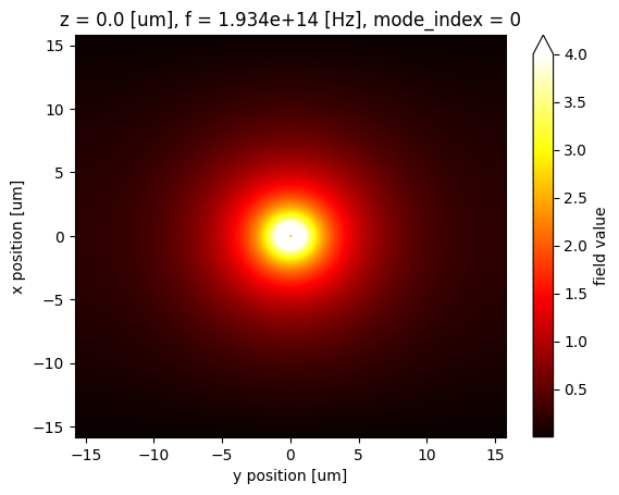
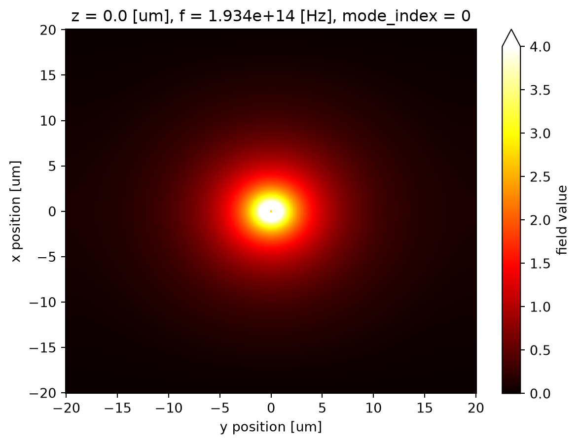
For instance, we can examine the mode profile of the waveguide with a width of 130 nm.
[13]:
optimal_mode = mode_data["w=0.13"]
optimal_mode.Ey.abs.plot(vmax=4, cmap="hot")
plt.show()
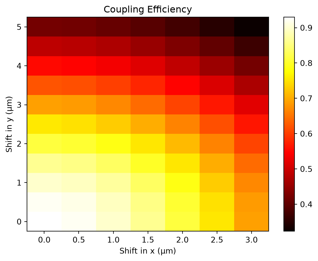
After determining the optimal waveguide geometry, we can examine the impact of misalignment on the coupling efficiency. This scenario becomes relevant as the fiber is often not perfectly aligned with the waveguide in practical situations. To accomplish this, we will employ the translated_copy(vector) method, which shifts the mode profile in both the \(x\) and \(y\) directions. Then we can calculate the overlap integral between the Gaussian beam and the shifted mode profile.
As anticipated, the results indicate that the coupling efficiency diminishes when the waveguide mode and Gaussian beam become misaligned.
[14]:
shift_x_list = np.linspace(0, 3, 7)
shift_y_list = np.linspace(0, 5, 11)

# use a nested list comprehension to build the array of overlaps
shifted_overlap = np.array(
    [
        [
            optimal_mode.translated_copy(vector=(shift_x, shift_y, 0))
            .outer_dot(gaussian_beam.field_data)
            .values.squeeze()
            for shift_x in shift_x_list
        ]
        for shift_y in shift_y_list
    ]
)

# plot the coupling efficiency
plt.pcolormesh(shift_x_list, shift_y_list, np.abs(shifted_overlap) ** 2, cmap="hot")
plt.xlabel("Shift in x (μm)")
plt.ylabel("Shift in y (μm)")
plt.title("Coupling Efficiency")
plt.colorbar()
plt.show()
Final Remarks#
In this example, we set the size of the Gaussian mode plane and waveguide mode plane to be identical. This is not strictly required for the overlap calculation. As long as both planes are sufficiently large and the mode profiles decay to zero at the boundaries, the result will be accurate. The discretization grids of the two profiles are not required to be identical either, since the outer_dot method will automatically interpolate the data. However, we need to ensure both grids are
sufficiently fine for the profiles to be accurate and to minimize discretization error in the integration.
The 3D FDTD simulation is the most accurate prediction of the coupling efficiency, as it captures the full physics at the facet, including reflection and radiation losses. The mode overlap approach, once corrected for the Fresnel reflection, is a fast and reliable approximation that agrees with FDTD to within a few percent. Because the mode solver is lightweight, it can be run locally with run_local without submitting any cloud task, which makes it well suited for quick design studies such
as the waveguide width optimization above.