
Dielectric to plasmonic waveguide coupler design via Bayesian#
optimization
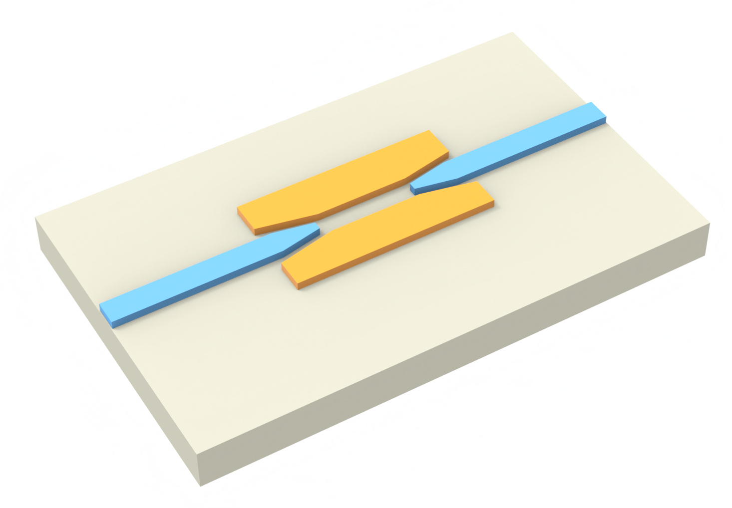
This notebook explores the design and simulation of a dielectric-to-plasmonic waveguide coupler using Tidy3D. Such couplers enable efficient transfer of optical signals from conventional silicon photonic waveguides to plasmonic waveguides, which support highly confined modes beyond the diffraction limit.
The coupler features a silicon strip waveguide that gradually tapers into a metallic slot waveguide. We utilize Bayesian optimization to systematically refine the design for maximum coupling efficiency.
[1]:
import matplotlib.pyplot as plt
import numpy as np
import tidy3d as td
import tidy3d.web as web
Base Simulation Setup#
Define central wavelength/frequency, a wavelength range, and its mapped frequency grid.
[2]:
# define frequency and wavelength range
lda0 = 1.50
freq0 = td.C_0 / lda0
ldas = np.linspace(1.45, 1.55, 21)
freqs = td.C_0 / ldas
fwidth = 0.5 * (np.max(freqs) - np.min(freqs))
Load silicon, silica, and gold mediums from the built-in material library for the coupler stack.
[3]:
si = td.material_library["cSi"]["Palik_LowLoss"]
sio2 = td.material_library["SiO2"]["Palik_LowLoss"]
au = td.material_library["Au"]["Olmon2012crystal"]
Set static geometric parameters such as the plasmonic slot length, silicon/gold layer thickness, slot width, and so on.
[4]:
l_slot = 1.5  # plasmonic waveguide length
h = 0.25  # both silicon and gold layer thicknesses are 250 nm
w_slot = 0.2  # metal slot width
w_si = 0.45  # silicon waveguide width
inf_eff = 1e2  # effective infinity
buffer = 0.6 * lda0  # buffer spacing to pad the simulation domain
To streamline the design optimization process, we define a function make_sim() which accepts tunable design parameters including the taper angle, taper tip width, and gap size, and constructs a corresponding Tidy3D Simulation object.
[5]:
# define the oxide layer
box = td.Structure(
    geometry=td.Box.from_bounds(rmin=(-inf_eff, -inf_eff, -inf_eff), rmax=(inf_eff, inf_eff, 0)),
    medium=sio2,
)

# add a mode source for excitation
mode_spec = td.ModeSpec(num_modes=1, target_neff=3.47)
mode_source = td.ModeSource(
    center=(-0.9 * buffer, 0, h / 2),
    size=(0, 4 * w_si, 6 * h),
    source_time=td.GaussianPulse(freq0=freq0, fwidth=fwidth),
    mode_spec=mode_spec,
    mode_index=0,
    direction="+",
    num_freqs=1,
)

# add a field monitor to visualize the field distribution
field_monitor = td.FieldMonitor(
    center=(0, 0, h / 2), size=(td.inf, td.inf, 0), freqs=[freq0], name="field"
)

# extrusion arguments for polyslab
polyslab_args = dict(axis=2, slab_bounds=(0, h))


# function to create a simulation given the design parameters
def make_sim(theta, d_tip, l_gap):
    # calculate the taper length
    l_taper = (w_si - d_tip) / (2 * np.tan(theta))

    # define the input waveguide structure
    vertices = [
        (-inf_eff, -w_si / 2),
        (0, -w_si / 2),
        (l_taper, -d_tip / 2),
        (l_taper, d_tip / 2),
        (0, w_si / 2),
        (-inf_eff, w_si / 2),
    ]
    wg_in = td.Structure(geometry=td.PolySlab(vertices=vertices, **polyslab_args), medium=si)

    # define the output waveguide structure
    vertices = [
        (l_taper + 2 * l_gap + l_slot, d_tip / 2),
        (2 * l_taper + 2 * l_gap + l_slot, w_si / 2),
        (inf_eff, w_si / 2),
        (inf_eff, -w_si / 2),
        (2 * l_taper + 2 * l_gap + l_slot, -w_si / 2),
        (l_taper + 2 * l_gap + l_slot, -d_tip / 2),
    ]
    wg_out = td.Structure(geometry=td.PolySlab(vertices=vertices, **polyslab_args), medium=si)

    # define the top plasmonic waveguide
    vertices = [
        (l_taper + l_gap, w_slot / 2),
        (l_taper + l_gap + l_slot, w_slot / 2),
        (inf_eff, np.tan(theta) * inf_eff),
        (-inf_eff, np.tan(theta) * inf_eff),
    ]
    gold_top = td.Structure(geometry=td.PolySlab(vertices=vertices, **polyslab_args), medium=au)

    # define the bottom plasmonic waveguide
    vertices = [
        (l_taper + l_gap, -w_slot / 2),
        (l_taper + l_gap + l_slot, -w_slot / 2),
        (inf_eff, -np.tan(theta) * inf_eff),
        (-inf_eff, -np.tan(theta) * inf_eff),
    ]
    gold_bottom = td.Structure(geometry=td.PolySlab(vertices=vertices, **polyslab_args), medium=au)

    # add a mode monitor to measure transmission
    mode_monitor = td.ModeMonitor(
        center=(2 * l_taper + l_slot + 2 * l_gap + 0.9 * buffer, 0, h / 2),
        size=mode_source.size,
        freqs=freqs,
        mode_spec=mode_spec,
        name="mode",
    )

    # define simulation
    sim = td.Simulation(
        center=(l_taper + l_gap + l_slot / 2, 0, h / 2),
        size=(2 * l_taper + 2 * l_gap + l_slot + 2 * buffer, w_si + 2 * buffer, h + 2 * buffer),
        grid_spec=td.GridSpec.auto(min_steps_per_wvl=20),
        boundary_spec=td.BoundarySpec(
            x=td.Boundary.absorber(num_layers=80),
            y=td.Boundary.absorber(),
            z=td.Boundary.pml(),
        ),
        run_time=5e-13,
        structures=[box, wg_in, wg_out, gold_top, gold_bottom],
        sources=[mode_source],
        monitors=[mode_monitor, field_monitor],
        symmetry=(0, -1, 0),
    )

    return sim
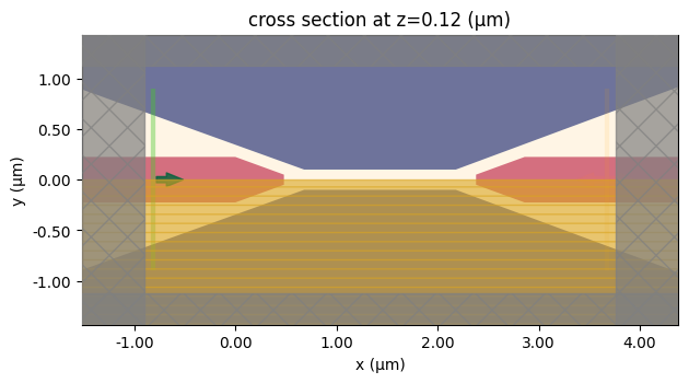
Build a first design instance and render a top view at z = h/2 to confirm geometry, source, and monitor locations.
[6]:
sim = make_sim(theta=np.deg2rad(20), d_tip=0.1, l_gap=0.2)
sim.plot(z=h / 2, monitor_alpha=0.1)
plt.show()
Submit the initial simulation to the cloud to generate fields and monitor data for the baseline geometry.
[7]:
sim_data = web.run(sim, "test run")
07:18:11 UTC Created task 'test run' with resource_id
             'fdve-2fa8f4a8-beaf-4c3f-b2d9-d9131863f3e3' and task_type 'FDTD'.
             View task using web UI at
             'https://tidy3d.simulation.cloud/workbench?taskId=fdve-2fa8f4a8-bea
             f-4c3f-b2d9-d9131863f3e3'.
Task folder: 'default'.
07:18:13 UTC Estimated FlexCredit cost: 0.320. This assumes the FDTD solver runs
             for the full simulation time; if early shutoff is reached, the
             billed cost can be lower. Use 'web.real_cost(task_id)' to get the
             billed FlexCredit cost after a simulation run.
07:18:15 UTC status = queued
             To cancel the simulation, use 'web.abort(task_id)' or
             'web.delete(task_id)' or abort/delete the task in the web UI.
             Terminating the Python script will not stop the job running on the
             cloud.
07:18:36 UTC starting up solver
07:18:37 UTC running solver
07:19:24 UTC early shutoff detected at 50%, exiting.
status = postprocess
07:19:27 UTC status = success
07:19:29 UTC View simulation result at
             'https://tidy3d.simulation.cloud/workbench?taskId=fdve-2fa8f4a8-bea
             f-4c3f-b2d9-d9131863f3e3'.
07:19:31 UTC Loading results from simulation_data.hdf5
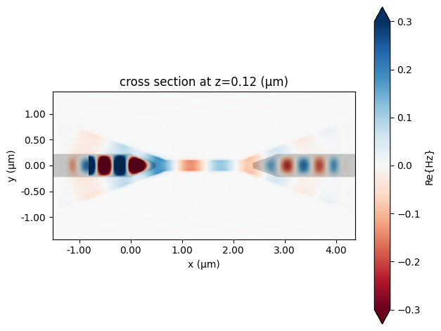
Plot the real part of Hz on the \(xy\) plane to inspect coupling in the initial (non‑optimized) geometry.
[8]:
sim_data.plot_field("field", "Hz", "real", vmax=0.3)
plt.show()
Bayesian Optimization#
Define an objective function that computes the average broadband transmission power in the fundamental mode based on simulation results. This serves as the figure of merit to be maximized during optimization.
For reference, the initial (unoptimized) device achieves a mean broadband transmission of 12.8%.
[9]:
def cal_transmission(sim_data):
    amp = sim_data["mode"].amps.sel(mode_index=0, direction="+").values
    T = np.abs(amp) ** 2
    return np.mean(T)


print(f"Transmission = {1e2 * cal_transmission(sim_data):.2f}%")
Transmission = 12.83%
Configure tidy3d.plugins.design to maximize transmission by sweeping theta, d_tip, and l_gap within bounds using a UCB (upper confidence bound) acquisition function.
[10]:
import tidy3d.plugins.design as tdd

# define optimization method
method = tdd.MethodBayOpt(
    initial_iter=10,
    n_iter=15,
    acq_func="ucb",
    kappa=0.3,
    seed=1,
)

# define optimization parameters
parameters = [
    tdd.ParameterFloat(name="theta", span=(np.deg2rad(5), np.deg2rad(20))),
    tdd.ParameterFloat(name="d_tip", span=(0.05, 0.2)),
    tdd.ParameterFloat(name="l_gap", span=(0.1, 0.3)),
]

# define a design space
design_space = tdd.DesignSpace(
    method=method, parameters=parameters, task_name="bay_opt", path_dir="./data"
)

# run the design optimization
results = design_space.run(make_sim, cal_transmission, verbose=True)
07:19:34 UTC Running 10 Simulations
07:21:28 UTC Best Fit from Initial Solutions: 0.368
Running 1 Simulations
07:22:03 UTC Running 1 Simulations
07:22:40 UTC Running 1 Simulations
07:23:58 UTC Latest Best Fit on Iter 2: 0.372
Running 1 Simulations
07:25:17 UTC Running 1 Simulations
07:27:11 UTC Running 1 Simulations
07:27:52 UTC Running 1 Simulations
07:28:31 UTC Latest Best Fit on Iter 6: 0.372
Running 1 Simulations
07:29:10 UTC Latest Best Fit on Iter 7: 0.373
Running 1 Simulations
07:29:48 UTC Running 1 Simulations
07:30:25 UTC Running 1 Simulations
07:31:45 UTC Running 1 Simulations
07:33:47 UTC Running 1 Simulations
07:35:06 UTC Latest Best Fit on Iter 12: 0.373
Running 1 Simulations
07:36:23 UTC Running 1 Simulations
07:37:02 UTC Best Result: 0.3727318964106043
             Best Parameters: theta: 0.1854948551302062 d_tip:
             0.16577642507210752 l_gap: 0.1
Rebuild the simulation with the best parameters from optimization.
[11]:
sim_opt = make_sim(**results.optimizer.max["params"])
sim_opt.plot(z=h / 2, monitor_alpha=0.2)
plt.show()
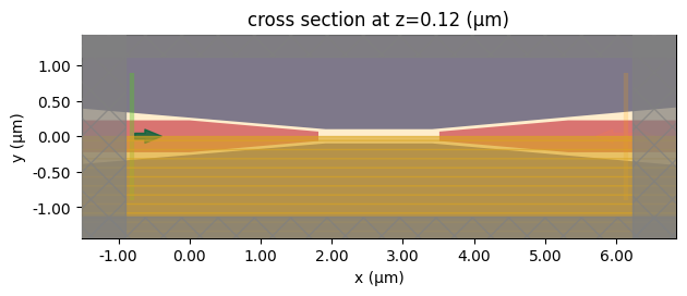
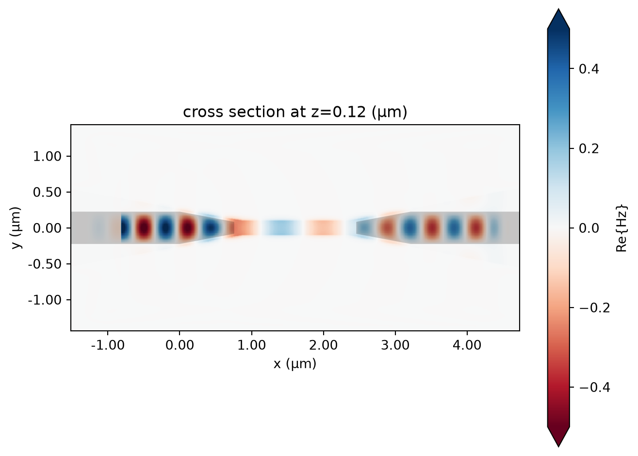
Run the optimized simulation (cached) again and plot the real part of Hz on the \(xy\) plane to confirm efficient coupling into the slot plasmonic mode.
[12]:
sim_data_opt = web.run(sim_opt, "optimal design")
sim_data_opt.plot_field("field", "Hz", "real", vmax=0.5)
plt.show()
             Loading simulation from local cache. View cached task using web UI
             at
             'https://tidy3d.simulation.cloud/workbench?taskId=fdve-e9560573-483
             f-4f09-9a48-320c449ff2ab'.
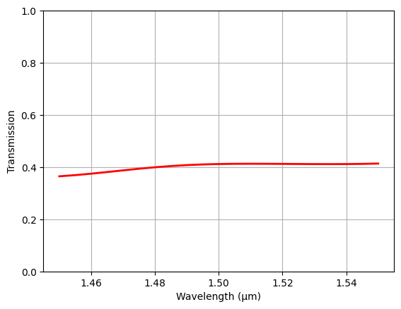
Finally, compute and plot power transmission from the mode monitor across the wavelength range.
[13]:
amp = sim_data_opt["mode"].amps.sel(mode_index=0, direction="+")
T = np.abs(amp) ** 2
plt.plot(ldas, T, c="red", linewidth=2)
plt.xlabel("Wavelength (μm)")
plt.ylabel("Transmission")
plt.ylim(0, 1)
plt.grid()
plt.show()