
Wavelength Plan and Thermal Budget

The chip the series arrives at, with the part this notebook works on marked:

The rings in Chip Layout are drawn to sit on eight channels. Fabrication moves them off, and each ring carries a heater to move it back. This notebook measures how far the rings move, how far a heater can move them, and what that costs in power.
Three quantities are measured:
Resonance sensitivity to geometry. A resonance is the round-trip length divided into wavelengths, so a change in radius, core width or core thickness shifts the channel. The sensitivity to each is measured by a finite-difference sweep over the technology.
Heater efficiency. A HEAT solve of the drawn modulator gives the ring temperature rise per milliwatt. Combined with the thermo-optic sensitivity from Component Library, that gives gigahertz per milliwatt.
Thermal crosstalk. Silicon conducts heat, so a heater warms neighbouring rings as well as its own. A second HEAT solve with two rings at the layout pitch measures how much.
Together these give the trim range the heaters must cover, the power that costs, and the energy per bit it adds to the link.
[1]:
%%capture

# Run the layout notebook, which brings in the chip and the channel plan
%run Optical_IO_Chip.ipynb
Progress: 100%
Progress: 100%
Progress: 100%
Progress: 100%
Progress: 100%
Progress: 100%
Progress: 100%
Progress: 100%
Progress: 100%
Progress: 100%
Progress: 100%
Progress: 100%
Progress: 100%
Progress: 100%
Progress: 100%
Progress: 100%
Progress: 100%
Progress: 100%
Progress: 100%
Progress: 100%
Progress: 100%
Progress: 100%
Progress: 100%
Progress: 100%
Progress: 100%
Progress: 100%
Progress: 100%
Progress: 100%
Progress: 100%
Progress: 100%
Progress: 100%
Progress: 100%
Progress: 100%
Progress: 100%
Progress: 100%
Progress: 100%
Progress: 100%
Progress: 100%
Progress: 100%
Progress: 100%
Progress: 100%
Progress: 100%
Progress: 100%
Progress: 100%
Progress: 100%
Progress: 100%
Progress: 100%
Progress: 100%
Progress: 100%
Progress: 100%
Progress: 100%
Progress: 100%
Progress: 100%
Progress: 100%
Progress: 100%
Progress: 100%
Progress: 100%
[2]:
import tidy3d as td
from tidy3d import web

p_probe = 1.0e-3  # Heater power used to probe the thermal response, W

# Read every layer height off the technology, so the two cannot drift apart
stack = tech.parametric_kwargs
z_wg = stack["core_thickness"] / 2  # mid core, where the mode is
z_heater = stack["core_thickness"] + stack["heater_separation"]
h_heater = stack["heater_thickness"]
clad_top = (
    z_heater + h_heater + stack["metal_separation"] + stack["metal_thickness"] + 1.0
)

h_box = 2.0  # Buried oxide thickness, um
die_thickness = 200.0  # Silicon substrate thickness after back-grinding, um

lateral_pad = 150.0  # Oxide added around the cell to form the domain, um
air_margin = 2.0  # Air above and below the die, so each boundary is an interface, um
What fabrication moves
A resonance sits where the round trip holds a whole number of wavelengths, so it follows the optical path length \(n_\text{eff} L\). Three fabrication parameters move it:
Ring radius changes the round-trip length directly, so \(\Delta f / f = -\Delta L / L\).
Core width and core thickness change the effective index. Silicon has high index contrast, so both sensitivities are large.
The radius term is arithmetic. The other two come from a bend mode solve at the perturbed geometry. The sweep runs at the technology level, since optical_io_soi takes the core width and thickness as arguments and rebuilds the port specification with them, which keeps the solved mode consistent with the geometry.
Step sizes are set by process control: a few nanometres on linewidth, a few more on SOI thickness.
The two spreads are treated separately. The wafer-scale spread is mostly common to eight rings within a millimetre of each other, and a common shift is corrected by moving the laser comb, at no cost on the chip. The within-die spread is the ring-to-ring difference, and only that has to be trimmed by the heaters.
[3]:
# Finite-difference steps for the sensitivity, um
steps = {"core_width": 0.006, "core_thickness": 0.004}

# One-sigma geometry spreads, nm: across a wafer, then between rings on a die
sigma_wafer = {"ring radius": 1.0, "core_width": 3.0, "core_thickness": 3.0}
sigma_die = {"ring radius": 0.3, "core_width": 0.5, "core_thickness": 0.3}


def rib_index(**geometry):
    """Bend mode index of the modulator waveguide, at a given core geometry."""
    # Rebuild the whole technology, so the port follows the geometry being swept
    t = optical_io_soi(**geometry)
    spec = t.ports["Rib_TE_1550_500"].copy()
    # Match the bend study's window and mode count, so only geometry differs
    spec.width, spec.limits, spec.added_solver_modes = (
        2 * r_target - 0.2,
        (-2.0, 2.0),
        6,
    )
    info = pf.port_modes(
        pf.Port((0, 0), 0, spec, bend_radius=r_target),
        frequencies=[f0],
        mesh_refinement=30,
        technology=t,
        verbose=False,
        show_progress=False,
    ).data.modes_info
    # Pick the guided mode by area, as the bend study does
    area = np.array(info["mode area"].values).ravel()
    return float(np.array(info["n eff"].values).ravel()[np.argmin(area)])


# Resonance sensitivity to each parameter, GHz per nm
sens = {"ring radius": f0 / r_target * 1e-3 * 1e-9}

for name, step in steps.items():
    base = stack[name]
    lo, hi = rib_index(**{name: base - step}), rib_index(**{name: base + step})
    # Difference the pair to get dn_eff, then convert that to a frequency shift
    sens[name] = abs(f0 * (hi - lo) / (2 * step) / b["n_group"] * 1e-3 * 1e-9)

print(
    f"{'what':16s} {'GHz/nm':>8s} {'wafer nm':>9s} {'GHz':>7s} "
    f"{'die nm':>7s} {'GHz':>7s}"
)
for k in sens:
    print(
        f"{k:16s} {sens[k]:8.1f} {sigma_wafer[k]:9.1f} "
        f"{sens[k]*sigma_wafer[k]:7.0f} {sigma_die[k]:7.1f} "
        f"{sens[k]*sigma_die[k]:7.0f}"
    )

# Total resonance spread, uncorrelated contributions in quadrature, GHz
wafer = np.sqrt(sum((sens[k] * sigma_wafer[k]) ** 2 for k in sens))
differential = np.sqrt(sum((sens[k] * sigma_die[k]) ** 2 for k in sens))
print(f"{'in quadrature':16s} {'':8s} {'':9s} {wafer:7.0f} {'':7s} {differential:7.0f}")
print()
print(
    f"wafer to wafer   {wafer:5.0f} GHz = {wafer/(fsr*1e-9):.2f} free spectral "
    f"ranges, taken out at the laser"
)
print(f"ring to ring     {differential:5.0f} GHz, one sigma, left to the heaters")

# Trim range the heaters must cover, GHz: three sigma either side
trim_range = 6 * differential
print()
print(f"three sigma either side is {trim_range:.0f} GHz of range")
print(f"at {ghz_per_k_rib:.2f} GHz/K that is {trim_range/ghz_per_k_rib:.1f} K")
print(f"against a modulator linewidth of {fwhm*1e-9:.0f} GHz")
what               GHz/nm  wafer nm     GHz  die nm     GHz
ring radius          38.7       1.0      39     0.3      12
core_width           40.9       3.0     123     0.5      20
core_thickness      130.2       3.0     391     0.3      39
in quadrature                           411              46

wafer to wafer     411 GHz = 0.17 free spectral ranges, taken out at the laser
ring to ring        46 GHz, one sigma, left to the heaters

three sigma either side is 274 GHz of range
at 9.31 GHz/K that is 29.4 K
against a modulator linewidth of 114 GHz
Core thickness dominates, at roughly three times the sensitivity of the radius per nanometre, and it is also the parameter least under the designer’s control, since it arrives with the wafer.
The last two columns separate the two spreads. Wafer to wafer the shift is a large fraction of a free spectral range, but common to all eight rings, so the laser comb absorbs it. Ring to ring within one die it is tens of gigahertz, and that is what the heaters must cover.
Heater efficiency
The sensitivities above are in gigahertz. Heater power is in milliwatts. A HEAT solve connects them by giving the ring temperature rise per milliwatt.
That figure depends on the whole stack and the package, not on the heater alone: heat leaves the ring through the buried oxide, spreads laterally in the silicon, and reaches the sink at the back of the die, so the die thickness enters the result.
Three points about the setup:
The substrate and cladding are added explicitly.
Component.extrudereturns the device layers, which is what the optical and charge solves need; a thermal problem also needs the material the heat flows into.The sink sits on a material interface, not on the domain edge, so the domain extends into air below the wafer.
Only the ring track is powered. The heater is one conductor from terminal to terminal, but dissipation follows current density, and the feed is drawn wide so little power lands there. A uniform rate over the whole polygon would put the hottest point in the fan-out.
[4]:
# Heater track width and feed slot width, read off the drawn cell, um
heater_width = mrm.parametric_kwargs["heater_width"]
heater_slot = mrm.parametric_kwargs["heater_slot"]

inset = 0.05 * heater_width  # Gap from the powered annulus to the metal faces, um
arc_r_out = r_target + heater_width / 2 - inset
arc_r_in = r_target - heater_width / 2 + inset
arc_height = 0.92 * h_heater
arc_fraction = 1 - 2 * np.arcsin(0.5 * heater_slot / r_target) / (2 * np.pi)
arc_volume = np.pi * (arc_r_out**2 - arc_r_in**2) * arc_height * arc_fraction


def arc_source(dx, name):
    """Overlay marking the powered part of one heater, centred at x = dx.

    An annulus with the feed slot removed, in the same metal as the track it
    sits inside, so it changes nothing but gives the source a region to act on.
    """
    z_mid = z_heater + h_heater / 2
    annulus = td.ClipOperation(
        operation="difference",
        geometry_a=td.Cylinder(
            center=(dx, 0, z_mid), radius=arc_r_out, length=arc_height, axis=2
        ),
        geometry_b=td.Cylinder(
            center=(dx, 0, z_mid), radius=arc_r_in, length=arc_height, axis=2
        ),
    )
    return td.Structure(
        geometry=td.ClipOperation(
            operation="difference",
            geometry_a=annulus,
            # Cut with a taller box, so its faces coincide with nothing
            geometry_b=td.Box(
                center=(dx, -r_target, z_mid),
                size=(heater_slot, heater_slot, 3 * h_heater),
            ),
        ),
        medium=tin["electrical"],
        name=name,
    )


def thermal(pitch=None, power=p_probe):
    """Solve one ring, or two at a given pitch with only the left one driven.

    Returns the temperature rise on the driven ring, the rise on the neighbour
    (nan when there is only one ring), and the data itself for plotting.
    """
    # Place one modulator per ring, then the powered overlay on each heater
    offsets = (0.0,) if pitch is None else (0.0, pitch)
    structures = []
    for dx in offsets:
        for s in mrm.extrude(classification="electrical"):
            t = s.to_tidy3d()
            structures.append(t.updated_copy(geometry=t.geometry.translated(dx, 0, 0)))
    structures += [arc_source(dx, f"heater{k}") for k, dx in enumerate(offsets)]

    # Size the domain: the cell, oxide around it, the die below, air either side
    (cx0, cy0), (cx1, cy1) = mrm.bounds()
    x0, x1 = cx0 - lateral_pad, cx1 + (pitch or 0.0) + lateral_pad
    y0, y1 = cy0 - lateral_pad, cy1 + lateral_pad
    z0, z1 = -h_box - die_thickness - air_margin, clad_top + air_margin

    # Add the box and the substrate, which the component extrusion does not draw
    wafer = td.Structure(
        geometry=td.Box.from_bounds((x0, y0, -h_box - die_thickness), (x1, y1, -h_box)),
        medium=si["electrical"],
        name="wafer",
    )
    clad = td.Structure(
        geometry=td.Box.from_bounds((x0, y0, -h_box), (x1, y1, clad_top)),
        medium=sio2["electrical"],
        name="clad",
    )

    # Refine a box around each ring, which distance grading alone would leave coarse
    refinement = [
        td.GridRefinementRegion(
            center=(dx, 0, 0.5 * (z_heater - h_box)),
            size=(6 * r_target, 6 * r_target, 2 * h_box + z_heater + 4),
            dl_internal=0.6,
            transition_thickness=1.5 * r_target,
        )
        for dx in offsets
    ]

    sim = td.HeatChargeSimulation(
        center=((x0 + x1) / 2, (y0 + y1) / 2, (z0 + z1) / 2),
        size=(x1 - x0, y1 - y0, z1 - z0),
        structures=[wafer, clad] + structures,
        medium=air["electrical"],
        # Drive the first ring only, as a volumetric rate over its heater arc
        sources=[td.HeatSource(structures=["heater0"], rate=power / arc_volume)],
        boundary_spec=[
            td.HeatBoundarySpec(
                placement=td.MediumMediumInterface(mediums=["Air", "SiO2"]),
                condition=td.ConvectionBC(
                    ambient_temperature=300, transfer_coeff=10e-12
                ),
            ),
            # Sink the heat at the back of the die, on the air to silicon interface
            td.HeatBoundarySpec(
                placement=td.MediumMediumInterface(mediums=["Air", "Si"]),
                condition=td.TemperatureBC(temperature=300),
            ),
        ],
        monitors=[
            td.TemperatureMonitor(
                size=(td.inf, td.inf, 0),
                center=(0, 0, z_wg),
                name="wg_plane",
                unstructured=True,
            )
        ],
        grid_spec=td.DistanceUnstructuredGrid(
            dl_interface=h_heater / 2,
            dl_bulk=25.0,
            distance_interface=h_heater,
            distance_bulk=h_box + 2,
            # Leave the substrate interior coarse, since nothing reads it
            non_refined_structures=["wafer"],
            mesh_refinements=refinement,
            # Allow elements far smaller than the domain, which is otherwise the floor
            relative_min_dl=0.5 * (h_heater / 2) / max(x1 - x0, y1 - y0, z1 - z0),
        ),
    )

    tag = "one" if pitch is None else f"pair{int(pitch)}"
    data = web.Job(simulation=sim, task_name=f"oio_heat_{tag}", verbose=False).run(
        path=f"heat_{tag}.hdf5"
    )

    def rise(x_centre):
        # Average over the ring core, read off the waveguide-plane monitor
        t = data["wg_plane"].temperature
        pts = np.asarray(t.points.values)
        vals = np.asarray(t.values).reshape(-1) - 300.0
        core = np.abs(np.hypot(pts[:, 0] - x_centre, pts[:, 1]) - r_target) < 0.25
        return vals[core].mean()

    return rise(0.0), (np.nan if pitch is None else rise(pitch)), data


driven, _, single_data = thermal()
k_per_mw = driven / (p_probe * 1e3)
ghz_per_mw = k_per_mw * ghz_per_k_rib

print(
    f"powered arc        {arc_fraction*100:.1f} percent of the circumference, "
    f"{arc_volume:.2f} um^3"
)
print(f"thermal impedance  {k_per_mw:.2f} K/mW")
print(f"tuning efficiency  {ghz_per_mw:.1f} GHz/mW = {ghz_per_mw/0.125:.0f} pm/mW")
print(f"one linewidth      {fwhm*1e-9/ghz_per_mw:.2f} mW")
powered arc        98.1 percent of the circumference, 3.67 um^3
thermal impedance  3.57 K/mW
tuning efficiency  33.2 GHz/mW = 266 pm/mW
one linewidth      3.44 mW
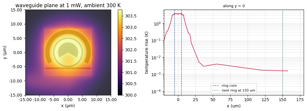
The temperature field below shows how far the heat spreads. It fills the oxide around the ring and reaches into the substrate, and that spread sets the crosstalk measured in the next section.
The square outline around the ring is the 90 nm silicon slab, which the modulator draws as one rectangle 8.2 um out from the ring centre, covering the ring and the bus together. Silicon conducts heat at 148e-6 W/(um K) against 1.38e-6 for the surrounding oxide, a factor of 107, so heat entering the slab spreads along it and the isotherms take its outline. Its extent is a layout constraint rather than a thermal choice: the slab has to reach past the outer contact plug, or the metal would sit on oxide at its edge.
[5]:
# Read the waveguide-plane monitor and convert to a rise above ambient
t = single_data["wg_plane"].temperature
pts = np.asarray(t.points.values)
vals = np.asarray(t.values).reshape(-1) - 300.0

fig, ax = plt.subplots(1, 2, figsize=(11, 3.8))

# Draw the temperature field, zoomed onto the ring from the die-scale domain
zoom = 3 * r_target
single_data.plot_field("wg_plane", ax=ax[0], cmap="inferno")
ax[0].set(
    xlim=(-zoom, zoom),
    ylim=(-zoom, zoom),
    aspect="equal",
    title=f"waveguide plane at {p_probe*1e3:.0f} mW, ambient 300 K",
)

# Take a cut along y = 0, which crosses the ring twice and then runs away
cut = np.abs(pts[:, 1]) < 0.3
order = np.argsort(pts[cut, 0])
ax[1].semilogy(
    pts[cut, 0][order], np.maximum(vals[cut][order], 1e-4), color="#c8385a", lw=1.4
)
# Mark where the cut crosses the ring core, on both sides
for sign in (-1, 1):
    ax[1].axvline(
        sign * r_target,
        color="#1f4e79",
        ls="--",
        lw=1,
        label="ring core" if sign > 0 else None,
    )

# Mark where the neighbouring ring sits, which is what the tail has to reach
ax[1].axvline(
    channel_pitch,
    color="#2e7d5b",
    ls=":",
    lw=1.4,
    label=f"next ring at {channel_pitch:.0f} um",
)
ax[1].set_title("along y = 0", fontsize=9)
ax[1].set_xlabel("x (um)")
ax[1].set_ylabel("temperature rise (K)")
ax[1].set_xlim(-20, channel_pitch * 1.2)
ax[1].legend(fontsize=8)
ax[1].grid(alpha=0.3, which="both")
plt.tight_layout()
plt.show()
Thermal crosstalk
All eight rings share one substrate, so power into one heater raises the temperature of the others and the bank is a coupled system. The coupling is set by how far heat spreads laterally before reaching the sink, which scales with die thickness, and by the ring pitch.
The solve below places a second ring at the transmit bank’s pitch and drives only the first. The second ring’s temperature rise gives the coupling directly.
[6]:
# Temperature rise on the driven ring and on its neighbour, K
driven_pair, neighbour, _ = thermal(pitch=channel_pitch)

# Crosstalk: neighbour rise as a fraction of the driven ring's
coupling = neighbour / driven_pair

print(f"pitch                      {channel_pitch:.0f} um")
print(f"driven ring                {driven_pair:.3f} K")
print(f"neighbour                  {neighbour:.4f} K")
print(f"coupling                   {coupling:.5f}")
print()

# Temperature the worst-case trim demands of one ring, K
worst_trim_k = trim_range / ghz_per_k_rib

# Resonance shift seven neighbours at that trim impose on one channel, GHz
neighbours_ghz = (n_channels - 1) * coupling * worst_trim_k * ghz_per_k_rib
print(f"worst trim on one ring     {worst_trim_k:.1f} K")
print(f"seven neighbours then add  {neighbours_ghz:.2f} GHz")
print(f"one linewidth is           {fwhm*1e-9:.0f} GHz")
print(f"margin                     {fwhm*1e-9/max(neighbours_ghz, 1e-9):.0f}x")
pitch                      150 um
driven ring                3.541 K
neighbour                  0.0003 K
coupling                   0.00008

worst trim on one ring     29.4 K
seven neighbours then add  0.15 GHz
one linewidth is           114 GHz
margin                     771x
The margin comes from the pitch, which is set by packaging rather than by thermal design: the bond pads in Chip Layout need 150 um per channel. At that spacing the coupling is several orders below the linewidth, so the eight channels can be controlled independently.
This is a result for this geometry, not a general one. Changing die_thickness or channel_pitch and re-running the same function gives a different coupling.
Tuning power
A heater can only raise a temperature, so the bank is drawn to the blue of its channels and every ring is corrected upward. The trim a given ring needs is then distributed between zero and the full spread rather than centred on zero, so the average is half the range and the worst case is all of it.
[7]:
mean_mw = trim_range / 2 / ghz_per_mw
worst_mw = trim_range / ghz_per_mw

print(f"{'':28s} {'per ring':>12s} {'eight rings':>14s}")
print(f"{'average trim':28s} {mean_mw:9.2f} mW {8*mean_mw:11.1f} mW")
print(f"{'worst case':28s} {worst_mw:9.2f} mW {8*worst_mw:11.1f} mW")
print()

# Aggregate line rate across the eight channels, bit/s
line_rate = n_channels * 100e9
print(f"tuning energy, average     {8*mean_mw*1e-3/line_rate*1e15:.1f} fJ/bit")
print(f"tuning energy, worst case  {8*worst_mw*1e-3/line_rate*1e15:.1f} fJ/bit")

# Save the measured constants, so the link notebook need not repeat these solves
np.savez(
    "thermal_budget.npz",
    k_per_mw=k_per_mw,
    ghz_per_mw=ghz_per_mw,
    coupling=coupling,
    trim_range=trim_range,
    differential=differential,
    mean_mw=mean_mw,
    worst_mw=worst_mw,
    pitch=channel_pitch,
    z_heater=z_heater,
    h_heater=h_heater,
    h_box=h_box,
    clad_top=clad_top,
    die_thickness=die_thickness,
    lateral_pad=lateral_pad,
    heater_width=heater_width,
    arc_volume=arc_volume,
)
                                 per ring    eight rings
average trim                      4.12 mW        33.0 mW
worst case                        8.24 mW        65.9 mW

tuning energy, average     41.2 fJ/bit
tuning energy, worst case  82.4 fJ/bit
Summary
Core thickness dominates the resonance spread, at roughly three times the sensitivity of the ring radius per nanometre, and it is fixed by the wafer rather than by the mask.
The wafer-scale spread is common mode. Rings a millimetre apart share most of it, so it is corrected by moving the laser comb. Correcting it with heaters instead would cost hundreds of milliwatts.
The within-die spread is what the heaters carry, tens of gigahertz against tens of gigahertz per milliwatt, so the eight rings trim for a few milliwatts in total.
Thermal crosstalk is negligible at this pitch, which the bond pads set, not the thermal design.
Link Simulation sets every heater on the chip from these numbers and drives the result with data.