
Technology and PDK Setup

This is the first of five notebooks that design an 8-channel microring transceiver for optical input and output between compute dies. The link uses one fiber, a multi-wavelength laser, a bank of microring modulators on a single bus, and a bank of ring drop filters that separates the channels again on the receive side.
The five notebooks are:
Technology and PDK Setup (this notebook): the process stack, with optical, thermal and electrical properties in one technology object.
Component Library: the microring modulator, the drop filters, the edge coupler and the detector, each with a model attached.
Chip Layout: the modulator bank, the demultiplexer bank, and the routing that connects them to the fiber and to the pads.
Wavelength Plan and Thermal Budget: how much heater power the channel plan costs, and how much of it leaks between neighbouring rings.
Link Simulation: eye diagrams and a link budget for the assembled chip.
The chip those five notebooks arrive at is below. Each stage adds one layer to it: the technology here, the devices next, then their placement, then the heater settings, and finally the data.

A microring resonance depends on the silicon geometry, on the free carriers in a reverse-biased junction, and on the local temperature set by a heater above the waveguide. Sizing the channel plan therefore requires a mode solve, a charge solve and a heat solve of the same structure.
This notebook defines one technology that all three read. Each medium carries optical properties and a MultiPhysicsMedium holding thermal conductivity, heat capacity, density and a semiconductor or conductor charge model. Layout drawn on it extrudes for FDTD or for HeatChargeSimulation without redefining any material.
The link
The chip carries 8 wavelength channels on a 200 GHz grid, each modulated at 100 Gb/s with non-return-to-zero (NRZ) signalling, for 800 Gb/s on a single fiber.
Parameter |
Value |
|---|---|
Channels |
8 |
Channel spacing |
200 GHz |
Line rate per channel |
100 Gb/s NRZ |
Aggregate rate |
800 Gb/s |
Ring radius |
5 um |
Silicon thickness |
220 nm, 90 nm slab |
Modulator |
lateral p-n junction, reverse biased |
Tuning |
TiN resistive heater per ring |
Detector |
germanium photodiode |
The ring radius and the channel plan are coupled. A ring resonates periodically, so the free spectral range (FSR) limits how many channels fit before the plan wraps onto the next resonance of the same ring. The FSR follows from the group index of the ring waveguide, measured at the end of this notebook.
Process stack
The stack is a generic 220 nm silicon-on-insulator platform with the layers an active ring needs: a partial etch for the rib waveguide, four implant levels for the junction and its ohmic contacts, germanium for the detectors, a resistive heater metal, and one thick routing metal.
Heights are measured from the bottom of the silicon device layer.
Level |
z (um) |
Material |
|---|---|---|
Buried oxide |
-2.0 to 0 |
SiO2 |
Silicon slab |
0 to 0.09 |
Si |
Silicon core |
0 to 0.22 |
Si |
Germanium |
0.22 to 0.72 |
Ge |
TiN heater |
1.02 to 1.14 |
TiN |
M1 routing |
1.60 to 3.60 |
Al |
Germanium sits directly on the silicon because it is grown epitaxially on it: the detector window is opened in the oxide and the exposed silicon seeds the crystal. That interface is both the p-side of the photodiode and the optical path, since light couples up into the germanium from the silicon waveguide below. The extrusion rule below intersects the germanium mask with the silicon mask, so germanium exists only where it has a seed.
Two numbers in this table are design choices rather than platform constants:
The heater sits 0.8 um above the silicon. A heater closer to the waveguide tunes more efficiently because less of its heat spreads sideways before reaching the mode, but the optical mode also starts to see the metal. Component Library, the next notebook in this series, measures the loss this separation costs.
The routing metal is 2 um thick, which keeps the resistance of the long heater feeds small compared with the heater itself, so the power lands in the ring and not in the wiring.
[1]:
import matplotlib.pyplot as plt
import numpy as np
import photonforge as pf
import tidy3d as td

# We raise the Tidy3D logging level to reduce output noise from the solves
# below. Warnings can flag real problems, so only suppress them once you have
# confirmed they are not relevant to your case.
td.config.logging.level = "ERROR"

lda0 = 1.55  # Design wavelength, um. Everything in this series references it.
f0 = pf.C_0 / lda0  # Design frequency, Hz
Materials
Each material is a dictionary with an "optical" entry and an "electrical" entry. PhotonForge picks the first for mode solving and FDTD, and the second when the layout is extruded for a heat or charge simulation.
Silicon appears five times: undoped, and at four implant levels, p and n for the junction and p++ and n++ for the ohmic contacts. All five share one SemiconductorMedium description, with band parameters and Caughey-Thomas mobility models for electrons and holes, and differ only in the doping concentration attached to it. Writing them through a small function keeps the
five definitions from drifting apart.
The junction implants are set at 7e17 cm^-3 acceptors and 5e17 cm^-3 donors. Depletion-type ring modulators sit in this range because the modulation efficiency and the optical loss come from the same free carriers: raising the doping shifts the resonance further per volt, and also absorbs more light. The ohmic implants are two orders of magnitude higher, at 1e20 cm^-3, so the contacts are not part of the junction’s series resistance.
[2]:
# Build one charge model, shared by every implant level
si_charge = td.SemiconductorMedium(
    permittivity=11.7,
    N_c=2.86e19,  # effective density of states, conduction band (cm^-3)
    N_v=3.1e19,  # effective density of states, valence band (cm^-3)
    E_g=1.11,  # silicon bandgap (eV)
    mobility_n=td.CaugheyThomasMobility(
        mu_min=52.2,
        mu=1471.0,
        ref_N=9.68e16,
        exp_N=0.68,
        exp_1=-0.57,
        exp_2=-2.33,
        exp_3=2.4,
        exp_4=-0.146,
    ),
    mobility_p=td.CaugheyThomasMobility(
        mu_min=44.9,
        mu=470.5,
        ref_N=2.23e17,
        exp_N=0.719,
        exp_1=-0.57,
        exp_2=-2.33,
        exp_3=2.4,
        exp_4=-0.146,
    ),
)

# Give silicon its thermal properties, in W/(um K), J/(kg K) and kg/um^3
si_heat = td.SolidSpec(conductivity=148e-6, capacity=711, density=2.33e-15)


def silicon(name, n_a=None, n_d=None):
    """Silicon at one implant level, as an optical and a multiphysics pair."""
    charge = si_charge
    if n_a is not None:
        charge = charge.updated_copy(N_a=[td.ConstantDoping(concentration=n_a)])
    if n_d is not None:
        charge = charge.updated_copy(N_d=[td.ConstantDoping(concentration=n_d)])
    return {
        "optical": td.material_library["cSi"]["Li1993_293K"],
        "electrical": td.MultiPhysicsMedium(
            # Static permittivity, which is all the charge solver reads
            optical=td.Medium(permittivity=11.7),
            heat=si_heat,
            charge=charge,
            name=name,
        ),
    }


si = silicon("Si")
si_p = silicon("Si p", n_a=7e17)  # junction acceptors
si_n = silicon("Si n", n_d=5e17)  # junction donors
si_pp = silicon("Si p++", n_a=1e20)  # ohmic contact implant
si_nn = silicon("Si n++", n_d=1e20)
The remaining materials are the cladding, the two metals, the tungsten plugs, the germanium and the air above the passivation opening.
Metals are described three ways at once. Optically they are dispersive media from the Tidy3D material library, or a perfect conductor where only the geometry matters. Thermally they carry the conductivity that drains heat away from the ring. Electrically they are ChargeConductorMedium objects, which is what the charge solver accepts for a contact.
Titanium nitride is not in the Tidy3D material library, so the heater uses measured index values for a sputtered film at 1550 nm. These vary with deposition conditions, so treat the optical part as representative rather than exact. Its electrical conductivity of 2.3 S/um is what sets the heater resistance, and that value is what matters for the tuning power in Wavelength Plan and Thermal Budget, later in this series.
[3]:
# Define the oxide, which is both the buried layer and the cladding
sio2 = {
    "optical": td.material_library["SiO2"]["Palik_Lossless"],
    "electrical": td.MultiPhysicsMedium(
        optical=td.Medium(permittivity=3.9),
        heat=td.SolidSpec(conductivity=1.38e-6, capacity=740, density=2.2e-15),
        charge=td.ChargeInsulatorMedium(permittivity=3.9),
        name="SiO2",
    ),
}

# Define the TiN heater metal, with n and k for a sputtered film at 1550 nm
tin = {
    "optical": td.medium_from_nk(n=2.6, k=4.2, freq=f0),
    "electrical": td.MultiPhysicsMedium(
        optical=td.PECMedium(),
        heat=td.SolidSpec(conductivity=29e-6, capacity=545, density=5.4e-15),
        charge=td.ChargeConductorMedium(conductivity=2.3),  # S/um
        name="TiN",
    ),
}

# Define the aluminium routing metal, which carries every net to its pad
al = {
    "optical": td.material_library["Al"]["Rakic1995"],
    "electrical": td.MultiPhysicsMedium(
        optical=td.PECMedium(),
        heat=td.SolidSpec(conductivity=237e-6, capacity=900, density=2.7e-15),
        charge=td.ChargeConductorMedium(conductivity=38),
        name="Al",
    ),
}

# Define the tungsten plugs, which reach from silicon and heater up to M1
w = {
    "optical": td.material_library["W"]["RakicLorentzDrude1998"],
    "electrical": td.MultiPhysicsMedium(
        optical=td.PECMedium(),
        heat=td.SolidSpec(conductivity=174e-6, capacity=132, density=19.3e-15),
        charge=td.ChargeConductorMedium(conductivity=18),
        name="W",
    ),
}

# Define the germanium of the detectors, optical and thermal properties only
ge = {
    "optical": td.material_library["Ge"]["Icenogle1976"],
    "electrical": td.MultiPhysicsMedium(
        optical=td.Medium(permittivity=16.0),
        heat=td.SolidSpec(conductivity=60e-6, capacity=320, density=5.32e-15),
        name="Ge",
    ),
}

# Define the air above the pad opening, as a fluid so the die top does not conduct
air = {
    "optical": td.Medium(permittivity=1),
    "electrical": td.MultiPhysicsMedium(
        optical=td.Medium(permittivity=1),
        heat=td.FluidSpec(),
        charge=td.ChargeInsulatorMedium(permittivity=1),
        name="Air",
    ),
}
The technology
A technology in PhotonForge has three parts: the drawing layers, the rules that turn masks into 3D structures, and the waveguide cross-sections used as ports.
Layers are the mask levels a designer draws on. Thirteen are enough for this chip.
Extrusion rules say which mask becomes which material over which range in z. Their order matters, since a later rule overrides an earlier one where they overlap. Two features of this stack depend on that:
The slab rule uses the union of the core and slab layers, so a rib waveguide only needs its core drawn on
"Si"and its surrounding slab on"Si Slab". The core rule then raises the silicon to full thickness where the core is drawn.Each implant needs two rules, because one drawn implant region covers both full-height core and thin slab and the two have different z limits. Drawing
"Si p++"on top of"Si p"gives the ohmic implant, since the later rule wins.
Ports define the two waveguide cross-sections used throughout the series: a 500 nm strip for routing, and the same width on a 90 nm slab for the rings. The rings use the rib cross-section because a lateral junction needs the slab to reach its contacts. Making the passive drop filters rib as well keeps their group index, and therefore their free spectral range, matched to the modulators.
Wrapping the definition in parametric_technology makes every stack dimension a keyword argument, so the same code can be re-evaluated at a different silicon thickness or heater separation.
[4]:
@pf.parametric_technology
def optical_io_soi(
    *,
    core_thickness=0.22,
    slab_thickness=0.09,
    ge_thickness=0.5,
    heater_separation=0.8,  # oxide between the silicon top and the heater
    heater_thickness=0.12,
    metal_separation=0.46,  # oxide between the heater top and M1
    metal_thickness=2.0,
    core_width=0.5,
    slab_width=5.0,  # Drawn slab of the rib port
    si=si,
    si_p=si_p,
    si_n=si_n,
    si_pp=si_pp,
    si_nn=si_nn,
    sio2=sio2,
    tin=tin,
    al=al,
    w=w,
    ge=ge,
    air=air,
):
    layers = {
        "Si": pf.LayerSpec(
            (1, 0), description="Full-thickness silicon", color="#1f4e7918", pattern="/"
        ),
        "Si Slab": pf.LayerSpec(
            (2, 0),
            description="Partially etched silicon slab",
            color="#4f8fc018",
            pattern="\\",
        ),
        "Si p": pf.LayerSpec(
            (3, 0), description="p implant", color="#c8385a18", pattern="."
        ),
        "Si n": pf.LayerSpec(
            (4, 0), description="n implant", color="#3aa59618", pattern="."
        ),
        "Si p++": pf.LayerSpec(
            (5, 0), description="p++ ohmic implant", color="#8b1c3818", pattern="x"
        ),
        "Si n++": pf.LayerSpec(
            (6, 0), description="n++ ohmic implant", color="#1c6b6118", pattern="x"
        ),
        "Ge": pf.LayerSpec(
            (7, 0), description="Germanium detector", color="#7a5c9918", pattern="+"
        ),
        "Contact": pf.LayerSpec(
            (10, 0),
            description="Tungsten plug on silicon",
            color="#88888818",
            pattern="solid",
        ),
        "Ge Contact": pf.LayerSpec(
            (11, 0),
            description="Tungsten plug on germanium",
            color="#66666618",
            pattern="solid",
        ),
        "Heater": pf.LayerSpec(
            (12, 0), description="TiN heater", color="#d4a01718", pattern="-"
        ),
        "Via": pf.LayerSpec(
            (13, 0),
            description="Via from heater to M1",
            color="#aaaaaa18",
            pattern="solid",
        ),
        "M1": pf.LayerSpec(
            (14, 0),
            description="Aluminium routing metal",
            color="#b0b0b018",
            pattern="solid",
        ),
        "Pad Open": pf.LayerSpec(
            (15, 0), description="Passivation opening", color="#00000018", pattern=":"
        ),
        # Two drawing layers that reach no mask: the chip area and the dicing street
        "FloorPlan": pf.LayerSpec(
            (99, 0), description="Chip area", color="#2e7d5b10", pattern="hollow"
        ),
        "Dicing": pf.LayerSpec(
            (98, 0), description="Dicing street", color="#c8385a10", pattern="hollow"
        ),
    }

    # Stack the layer heights up from z = 0, the bottom of the device silicon
    z_ge = core_thickness + ge_thickness
    z_heater = core_thickness + heater_separation
    z_metal = z_heater + heater_thickness + metal_separation

    # Mask the slab from both silicon layers and the core from the unetched one
    slab_mask = pf.MaskSpec([(1, 0), (2, 0)])
    core_mask = pf.MaskSpec((1, 0))

    # Passivation opening, dilated because the etch undercuts the drawn edge
    pad_mask = pf.MaskSpec((15, 0), dilation=0.2)

    extrusion_specs = [
        # Fill the opening with air, then put the oxide back below the metal
        pf.ExtrusionSpec(pad_mask, air, (0, pf.Z_INF)),
        pf.ExtrusionSpec(pad_mask, sio2, (0, z_metal + metal_thickness)),
        pf.ExtrusionSpec(slab_mask, si, (0, slab_thickness)),
        pf.ExtrusionSpec(core_mask, si, (0, core_thickness)),
    ]

    # Draw each implant twice, once on the core and once on the slab
    for layer, medium in (
        ((3, 0), si_p),
        ((4, 0), si_n),
        ((5, 0), si_pp),
        ((6, 0), si_nn),
    ):
        mask = pf.MaskSpec(layer)
        extrusion_specs.append(
            pf.ExtrusionSpec(mask * (2, 0), medium, (0, slab_thickness))
        )
        extrusion_specs.append(
            pf.ExtrusionSpec(mask * (1, 0), medium, (0, core_thickness))
        )

    extrusion_specs += [
        # Intersect germanium with silicon, since it grows on a silicon seed
        pf.ExtrusionSpec(pf.MaskSpec((7, 0)) * (1, 0), ge, (core_thickness, z_ge)),
        # Raise each plug from the surface it lands on to the bottom of M1
        pf.ExtrusionSpec(pf.MaskSpec((10, 0)), w, (slab_thickness, z_metal)),
        pf.ExtrusionSpec(pf.MaskSpec((11, 0)), w, (z_ge, z_metal)),
        pf.ExtrusionSpec(
            pf.MaskSpec((12, 0)), tin, (z_heater, z_heater + heater_thickness)
        ),
        pf.ExtrusionSpec(
            pf.MaskSpec((13, 0)), w, (z_heater + heater_thickness, z_metal)
        ),
        pf.ExtrusionSpec(
            pf.MaskSpec((14, 0)), al, (z_metal, z_metal + metal_thickness)
        ),
    ]

    ports = {
        "TE_1550_500": pf.PortSpec(
            description="Strip waveguide, TE, 500 nm",
            width=3.0,  # Mode solver window
            limits=(-1.0, 1.0),
            num_modes=1,
            target_neff=3.5,  # Starting guess for the effective index
            path_profiles=[(core_width, 0, (1, 0))],
        ),
        "Rib_TE_1550_500": pf.PortSpec(
            description="Rib waveguide on 90 nm slab, TE, 500 nm",
            width=4.0,  # Mode solver window
            limits=(-1.0, 1.0),
            num_modes=1,
            target_neff=2.5,  # Starting guess for the effective index
            path_profiles=[(core_width, 0, (1, 0)), (slab_width, 0, (2, 0))],
        ),
    }

    return pf.Technology(
        name="Optical I/O SOI",
        version="1.0",
        layers=layers,
        extrusion_specs=extrusion_specs,
        ports=ports,
        # Fill everything no rule covers with oxide, so the cladding needs no mask
        background_medium=sio2,
    )


tech = optical_io_soi()
pf.config.default_technology = tech
The three tables below list the drawing layers, the extrusion rules that turn them into solids, and the port cross-sections.
[5]:
# Every drawing layer with its number, datatype and description
tech.layers
[5]:
| Name | Layer | Description | Color | Pattern | Device marker | Conductive | Min. width (μm) | Min. spacing (μm) |
|---|---|---|---|---|---|---|---|---|
| Si | (1, 0) | Full-thickness silicon | #1f4e7918 | / | ||||
| Si Slab | (2, 0) | Partially etched silicon slab | #4f8fc018 | \ | ||||
| Si p | (3, 0) | p implant | #c8385a18 | . | ||||
| Si n | (4, 0) | n implant | #3aa59618 | . | ||||
| Si p++ | (5, 0) | p++ ohmic implant | #8b1c3818 | x | ||||
| Si n++ | (6, 0) | n++ ohmic implant | #1c6b6118 | x | ||||
| Ge | (7, 0) | Germanium detector | #7a5c9918 | + | ||||
| Contact | (10, 0) | Tungsten plug on silicon | #88888818 | solid | ||||
| Ge Contact | (11, 0) | Tungsten plug on germanium | #66666618 | solid | ||||
| Heater | (12, 0) | TiN heater | #d4a01718 | - | ||||
| Via | (13, 0) | Via from heater to M1 | #aaaaaa18 | solid | ||||
| M1 | (14, 0) | Aluminium routing metal | #b0b0b018 | solid | ||||
| Pad Open | (15, 0) | Passivation opening | #00000018 | : | ||||
| Dicing | (98, 0) | Dicing street | #c8385a10 | hollow | ||||
| FloorPlan | (99, 0) | Chip area | #2e7d5b10 | hollow |
[6]:
# Every extrusion rule, with its z extent and the medium it makes
tech.extrusion_specs
[6]:
| # | Mask | Limits (μm) | Sidewall (°) | Opt. Medium | Elec. Medium |
|---|---|---|---|---|---|
| 0 | 'Pad Open'**0.2 | 0, inf | 0 | Medium() | MultiPhysicsMedium(name='Air',…… optical={}, heat={}, charge={}) |
| 1 | 'Pad Open'**0.2 | 0, 3.6 | 0 | SiO2_Palik_LowLoss | MultiPhysicsMedium(name='SiO2',…… optical={'permittivity': 3.9}, heat={'capacity': 740.0, 'conductivity': 1.38e-06, 'density': 2.2e-15}, charge={'permittivity': 3.9}) |
| 2 | 'Si' + 'Si Slab' | 0, 0.09 | 0 | cSi_Li1993_293K | MultiPhysicsMedium(name='Si',…… optical={'permittivity': 11.7}, heat={'capacity': 711.0, 'conductivity': 0.000148, 'density': 2.33e-15}, charge={'permittivity': 11.7, 'N_c': {'N': 2.86e+19}, 'N_v': {'N': 3.1e+19}, 'E_g': {'eg': 1.11}, 'mobility_n': {'mu_min': 52.2, 'mu': 1471.0, 'exp_2': -2.33, 'exp_N': 0.68, 'ref_N': 9.68e+16, 'exp_1': -0.57, 'exp_3': 2.4, 'exp_4': -0.146}, 'mobility_p': {'mu_min': 44.9, 'mu': 470.5, 'exp_2': -2.33, 'exp_N': 0.719, 'ref_N': 2.23e+17, 'exp_1': -0.57, 'exp_3': 2.4, 'exp_4': -0.146}}) |
| 3 | 'Si' | 0, 0.22 | 0 | cSi_Li1993_293K | MultiPhysicsMedium(name='Si',…… optical={'permittivity': 11.7}, heat={'capacity': 711.0, 'conductivity': 0.000148, 'density': 2.33e-15}, charge={'permittivity': 11.7, 'N_c': {'N': 2.86e+19}, 'N_v': {'N': 3.1e+19}, 'E_g': {'eg': 1.11}, 'mobility_n': {'mu_min': 52.2, 'mu': 1471.0, 'exp_2': -2.33, 'exp_N': 0.68, 'ref_N': 9.68e+16, 'exp_1': -0.57, 'exp_3': 2.4, 'exp_4': -0.146}, 'mobility_p': {'mu_min': 44.9, 'mu': 470.5, 'exp_2': -2.33, 'exp_N': 0.719, 'ref_N': 2.23e+17, 'exp_1': -0.57, 'exp_3': 2.4, 'exp_4': -0.146}}) |
| 4 | 'Si p' * 'Si Slab' | 0, 0.09 | 0 | cSi_Li1993_293K | MultiPhysicsMedium(name='Si p',…… optical={'permittivity': 11.7}, heat={'capacity': 711.0, 'conductivity': 0.000148, 'density': 2.33e-15}, charge={'permittivity': 11.7, 'N_c': {'N': 2.86e+19}, 'N_v': {'N': 3.1e+19}, 'E_g': {'eg': 1.11}, 'mobility_n': {'mu_min': 52.2, 'mu': 1471.0, 'exp_2': -2.33, 'exp_N': 0.68, 'ref_N': 9.68e+16, 'exp_1': -0.57, 'exp_3': 2.4, 'exp_4': -0.146}, 'mobility_p': {'mu_min': 44.9, 'mu': 470.5, 'exp_2': -2.33, 'exp_N': 0.719, 'ref_N': 2.23e+17, 'exp_1': -0.57, 'exp_3': 2.4, 'exp_4': -0.146}, 'N_a': ({'concentration': 7e+17},)}) |
| 5 | 'Si p' * 'Si' | 0, 0.22 | 0 | cSi_Li1993_293K | MultiPhysicsMedium(name='Si p',…… optical={'permittivity': 11.7}, heat={'capacity': 711.0, 'conductivity': 0.000148, 'density': 2.33e-15}, charge={'permittivity': 11.7, 'N_c': {'N': 2.86e+19}, 'N_v': {'N': 3.1e+19}, 'E_g': {'eg': 1.11}, 'mobility_n': {'mu_min': 52.2, 'mu': 1471.0, 'exp_2': -2.33, 'exp_N': 0.68, 'ref_N': 9.68e+16, 'exp_1': -0.57, 'exp_3': 2.4, 'exp_4': -0.146}, 'mobility_p': {'mu_min': 44.9, 'mu': 470.5, 'exp_2': -2.33, 'exp_N': 0.719, 'ref_N': 2.23e+17, 'exp_1': -0.57, 'exp_3': 2.4, 'exp_4': -0.146}, 'N_a': ({'concentration': 7e+17},)}) |
| 6 | 'Si n' * 'Si Slab' | 0, 0.09 | 0 | cSi_Li1993_293K | MultiPhysicsMedium(name='Si n',…… optical={'permittivity': 11.7}, heat={'capacity': 711.0, 'conductivity': 0.000148, 'density': 2.33e-15}, charge={'permittivity': 11.7, 'N_c': {'N': 2.86e+19}, 'N_v': {'N': 3.1e+19}, 'E_g': {'eg': 1.11}, 'mobility_n': {'mu_min': 52.2, 'mu': 1471.0, 'exp_2': -2.33, 'exp_N': 0.68, 'ref_N': 9.68e+16, 'exp_1': -0.57, 'exp_3': 2.4, 'exp_4': -0.146}, 'mobility_p': {'mu_min': 44.9, 'mu': 470.5, 'exp_2': -2.33, 'exp_N': 0.719, 'ref_N': 2.23e+17, 'exp_1': -0.57, 'exp_3': 2.4, 'exp_4': -0.146}, 'N_d': ({'concentration': 5e+17},)}) |
| 7 | 'Si n' * 'Si' | 0, 0.22 | 0 | cSi_Li1993_293K | MultiPhysicsMedium(name='Si n',…… optical={'permittivity': 11.7}, heat={'capacity': 711.0, 'conductivity': 0.000148, 'density': 2.33e-15}, charge={'permittivity': 11.7, 'N_c': {'N': 2.86e+19}, 'N_v': {'N': 3.1e+19}, 'E_g': {'eg': 1.11}, 'mobility_n': {'mu_min': 52.2, 'mu': 1471.0, 'exp_2': -2.33, 'exp_N': 0.68, 'ref_N': 9.68e+16, 'exp_1': -0.57, 'exp_3': 2.4, 'exp_4': -0.146}, 'mobility_p': {'mu_min': 44.9, 'mu': 470.5, 'exp_2': -2.33, 'exp_N': 0.719, 'ref_N': 2.23e+17, 'exp_1': -0.57, 'exp_3': 2.4, 'exp_4': -0.146}, 'N_d': ({'concentration': 5e+17},)}) |
| 8 | 'Si p++' * 'Si Slab' | 0, 0.09 | 0 | cSi_Li1993_293K | MultiPhysicsMedium(name='Si…… p++', optical={'permittivity': 11.7}, heat={'capacity': 711.0, 'conductivity': 0.000148, 'density': 2.33e-15}, charge={'permittivity': 11.7, 'N_c': {'N': 2.86e+19}, 'N_v': {'N': 3.1e+19}, 'E_g': {'eg': 1.11}, 'mobility_n': {'mu_min': 52.2, 'mu': 1471.0, 'exp_2': -2.33, 'exp_N': 0.68, 'ref_N': 9.68e+16, 'exp_1': -0.57, 'exp_3': 2.4, 'exp_4': -0.146}, 'mobility_p': {'mu_min': 44.9, 'mu': 470.5, 'exp_2': -2.33, 'exp_N': 0.719, 'ref_N': 2.23e+17, 'exp_1': -0.57, 'exp_3': 2.4, 'exp_4': -0.146}, 'N_a': ({'concentration': 1e+20},)}) |
| 9 | 'Si p++' * 'Si' | 0, 0.22 | 0 | cSi_Li1993_293K | MultiPhysicsMedium(name='Si…… p++', optical={'permittivity': 11.7}, heat={'capacity': 711.0, 'conductivity': 0.000148, 'density': 2.33e-15}, charge={'permittivity': 11.7, 'N_c': {'N': 2.86e+19}, 'N_v': {'N': 3.1e+19}, 'E_g': {'eg': 1.11}, 'mobility_n': {'mu_min': 52.2, 'mu': 1471.0, 'exp_2': -2.33, 'exp_N': 0.68, 'ref_N': 9.68e+16, 'exp_1': -0.57, 'exp_3': 2.4, 'exp_4': -0.146}, 'mobility_p': {'mu_min': 44.9, 'mu': 470.5, 'exp_2': -2.33, 'exp_N': 0.719, 'ref_N': 2.23e+17, 'exp_1': -0.57, 'exp_3': 2.4, 'exp_4': -0.146}, 'N_a': ({'concentration': 1e+20},)}) |
| 10 | 'Si n++' * 'Si Slab' | 0, 0.09 | 0 | cSi_Li1993_293K | MultiPhysicsMedium(name='Si…… n++', optical={'permittivity': 11.7}, heat={'capacity': 711.0, 'conductivity': 0.000148, 'density': 2.33e-15}, charge={'permittivity': 11.7, 'N_c': {'N': 2.86e+19}, 'N_v': {'N': 3.1e+19}, 'E_g': {'eg': 1.11}, 'mobility_n': {'mu_min': 52.2, 'mu': 1471.0, 'exp_2': -2.33, 'exp_N': 0.68, 'ref_N': 9.68e+16, 'exp_1': -0.57, 'exp_3': 2.4, 'exp_4': -0.146}, 'mobility_p': {'mu_min': 44.9, 'mu': 470.5, 'exp_2': -2.33, 'exp_N': 0.719, 'ref_N': 2.23e+17, 'exp_1': -0.57, 'exp_3': 2.4, 'exp_4': -0.146}, 'N_d': ({'concentration': 1e+20},)}) |
| 11 | 'Si n++' * 'Si' | 0, 0.22 | 0 | cSi_Li1993_293K | MultiPhysicsMedium(name='Si…… n++', optical={'permittivity': 11.7}, heat={'capacity': 711.0, 'conductivity': 0.000148, 'density': 2.33e-15}, charge={'permittivity': 11.7, 'N_c': {'N': 2.86e+19}, 'N_v': {'N': 3.1e+19}, 'E_g': {'eg': 1.11}, 'mobility_n': {'mu_min': 52.2, 'mu': 1471.0, 'exp_2': -2.33, 'exp_N': 0.68, 'ref_N': 9.68e+16, 'exp_1': -0.57, 'exp_3': 2.4, 'exp_4': -0.146}, 'mobility_p': {'mu_min': 44.9, 'mu': 470.5, 'exp_2': -2.33, 'exp_N': 0.719, 'ref_N': 2.23e+17, 'exp_1': -0.57, 'exp_3': 2.4, 'exp_4': -0.146}, 'N_d': ({'concentration': 1e+20},)}) |
| 12 | 'Ge' * 'Si' | 0.22, 0.72 | 0 | Ge_Icenogle1976 | MultiPhysicsMedium(name='Ge',…… optical={'permittivity': 16.0}, heat={'capacity': 320.0, 'conductivity': 6e-05, 'density': 5.32e-15}) |
| 13 | 'Contact' | 0.09, 1.6 | 0 | W_RakicLorentzDrude1998 | MultiPhysicsMedium(name='W',…… optical={}, heat={'capacity': 132.0, 'conductivity': 0.000174, 'density': 1.93e-14}, charge={'conductivity': 18.0}) |
| 14 | 'Ge Contact' | 0.72, 1.6 | 0 | W_RakicLorentzDrude1998 | MultiPhysicsMedium(name='W',…… optical={}, heat={'capacity': 132.0, 'conductivity': 0.000174, 'density': 1.93e-14}, charge={'conductivity': 18.0}) |
| 15 | 'Heater' | 1.02, 1.14 | 0 | Lorentz(coeffs=……((21.840000000000003, 162323815372577.7, 52562735135327.414),)) | MultiPhysicsMedium(name='TiN',…… optical={}, heat={'capacity': 545.0, 'conductivity': 2.9e-05, 'density': 5.4e-15}, charge={'conductivity': 2.3}) |
| 16 | 'Via' | 1.14, 1.6 | 0 | W_RakicLorentzDrude1998 | MultiPhysicsMedium(name='W',…… optical={}, heat={'capacity': 132.0, 'conductivity': 0.000174, 'density': 1.93e-14}, charge={'conductivity': 18.0}) |
| 17 | 'M1' | 1.6, 3.6 | 0 | Al_Rakic1995 | MultiPhysicsMedium(name='Al',…… optical={}, heat={'capacity': 900.0, 'conductivity': 0.000237, 'density': 2.7e-15}, charge={'conductivity': 38.0}) |
[7]:
# Every port, with its window, layer stack and mode count
tech.ports
[7]:
| Name | Classification | Description | Width (μm) | Limits (μm) | Radius (μm) | Modes | Target n_eff | Path profiles (μm) |
|---|---|---|---|---|---|---|---|---|
| Rib_TE_1550_500 | optical | Rib waveguide on 90 nm slab,…… TE, 500 nm | 4 | -1, 1 | 0 | 1 | 2.5 | 'Si': 0.5, 'Si Slab': 5 |
| TE_1550_500 | optical | Strip waveguide, TE, 500 nm | 3 | -1, 1 | 0 | 1 | 3.5 | 'Si': 0.5 |
Cross-section check
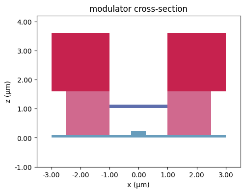
Extrusion rules are easiest to check by drawing a cross-section and plotting it. The component below is the modulator cross-section: a rib waveguide with a lateral junction, ohmic implants set back from the mode, tungsten plugs on the slab, the heater above the core and routing metal on top.
The implants are drawn as overlapping rectangles rather than abutting ones. The p implant covers everything left of the junction and the p++ implant covers its outer part, so extrusion order sets each boundary. A change to the ohmic setback then moves one edge instead of two.
[8]:
# Build a test cell of plain rectangles, one for each drawing layer
xs = pf.Component("cross_section")
xs.add(
    # Partially etched slab, then the unetched rib core on top of it
    "Si Slab",
    pf.Rectangle((-3, -2), (3, 2)),
    "Si",
    pf.Rectangle((-0.25, -2), (0.25, 2)),
    # Add the p and n implants, meeting at x = 0 in the middle of the core
    "Si p",
    pf.Rectangle((-3, -2), (0, 2)),
    "Si n",
    pf.Rectangle((0, -2), (3, 2)),
    # Add the ohmic implants, starting 0.8 um out where the mode cannot reach
    "Si p++",
    pf.Rectangle((-3, -2), (-0.8, 2)),
    "Si n++",
    pf.Rectangle((0.8, -2), (3, 2)),
    # Tungsten plugs land on the ohmic implants, one on each side
    "Contact",
    pf.Rectangle((-2.5, -2), (-1.0, 2)),
    pf.Rectangle((1.0, -2), (2.5, 2)),
    # Heater metal above the core, routing metal above that
    "Heater",
    pf.Rectangle((-1.0, -2), (1.0, 2)),
    "M1",
    pf.Rectangle((-3, -2), (-1.0, 2)),
    pf.Rectangle((1.0, -2), (3, 2)),
)

# Draw the stack the extrusion rules produced, cut along y = 0
fig, ax = plt.subplots(1, 1, figsize=(7, 4))
pf.tidy3d_plot(xs, y=0, ax=ax, plot_type="structures", frequency=f0)
ax.set_xlim(-3.5, 3.5)
ax.set_ylim(-1.0, 4.2)
ax.set_title("modulator cross-section")
plt.show()
Waveguide indices and the wavelength plan
With the stack defined, the two port specifications can be solved for their modes. The group index of the rib waveguide is the number the channel plan depends on: it fixes the free spectral range of a ring of a given radius, through
A 5 um ring is small enough that its FSR is wide compared with the 1.6 THz the channel plan spans, which is what allows eight channels to be placed without any of them landing on a neighbouring resonance of the same ring.
[9]:
r_ring = 5.0  # ring radius used throughout the series (um)
length = 2 * np.pi * r_ring

solved = {}
for name in tech.ports:
    # Solve the port mode, over three frequencies so the group index comes out
    solved[name] = pf.port_modes(
        name, [f0], group_index=True, show_progress=False, verbose=False
    )
    n_eff = float(np.real(solved[name].data.n_eff.values.ravel()[0]))
    n_group = float(np.real(solved[name].data.n_group.values.ravel()[0]))
    print(f"{name:18s}  n_eff = {n_eff:.4f}   n_group = {n_group:.4f}")

# Group index of the rib mode, which is the one that runs around the rings
n_group = float(np.real(solved["Rib_TE_1550_500"].data.n_group.values.ravel()[0]))

fsr = pf.C_0 / (n_group * length)
print(f"\nring radius {r_ring} um, round trip {length:.2f} um")
print(f"FSR = {fsr * 1e-9:.0f} GHz = {lda0**2 / (n_group * length) * 1e3:.1f} nm")
n_channels, channel_grid = 8, 200e9  # Channel count and spacing for this link

# Eight channels sit on seven gaps, so the comb is seven spacings wide
channel_span = (n_channels - 1) * channel_grid
print(
    f"{n_channels} channels at {channel_grid*1e-9:.0f} GHz span "
    f"{channel_span*1e-9:.0f} GHz = {channel_span / fsr * 100:.0f}% of one FSR"
)
Rib_TE_1550_500     n_eff = 2.5621   n_group = 3.8804
TE_1550_500         n_eff = 2.4395   n_group = 4.1775

ring radius 5.0 um, round trip 31.42 um
FSR = 2459 GHz = 19.7 nm
8 channels at 200 GHz span 1400 GHz = 57% of one FSR
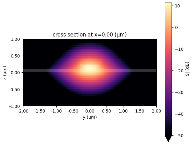
The mode profile shows whether the port width is sufficient, since the field has to have decayed at the window edge. The rib mode spreads further than the strip mode because the slab guides part of it sideways, which is why the two port specifications use different widths. On a logarithmic scale the field at the edge of the 4 um window sits far below the peak, so the window is not clipping the mode.
The rib slab is drawn wider than that window on purpose. Port detection then matches any component whose slab fills the window, rather than only a slab of one particular width, and a modulator slab is many microns across.
That choice decides target_neff, the effective index the mode solver starts its search from. It keeps the modes nearest that guess, so the guess has to sit near the mode that is wanted. Once the slab fills the window, a bend in this waveguide also supports radiating solutions, at 2.89 and 2.92 against the guided 2.58, and a guess at the silicon core index returns one of those instead: a field pressed against the inner wall of the bend, carrying twenty thousand decibels per centimetre. The
rings make every rib port a bent one, so the guess is set near the guided index.
[10]:
# Plot the rib mode, reusing the solve from the cell above
solved["Rib_TE_1550_500"].plot_field(
    "S", val="abs", scale="dB", mode_index=0, f=f0, robust=False, vmin=-50
)
plt.show()
The same layout, for heat and charge
Everything so far used the optical half of each material. Passing classification="electrical" to Component.extrude extrudes the identical layout with the multiphysics half instead. Each solid it returns carries its own medium and converts with to_tidy3d, producing structures that a HeatChargeSimulation accepts directly.
Component Library and Wavelength Plan and Thermal Budget rely on this: the heater arc, the junction and the waveguide are drawn once, and the thermal impedance, the capacitance-voltage curve and the mode index all come from that single drawing.
[11]:
# Extrude the same cell again, now selecting the multiphysics media
structures = [x.to_tidy3d() for x in xs.extrude(classification="electrical")]
print(f"{len(structures)} structures:", sorted({s.medium.name for s in structures}))

# Collect the structures in a Scene, which is enough to draw their properties
scene = td.Scene(structures=structures, medium=sio2["electrical"])

# Put the two square panels on top and the wide doping zoom across the bottom
fig = plt.figure(figsize=(12.5, 8), constrained_layout=True)
grid = fig.add_gridspec(2, 2, height_ratios=(2.4, 1))
ax_heat, ax_charge = fig.add_subplot(grid[0, 0]), fig.add_subplot(grid[0, 1])
ax_dope = fig.add_subplot(grid[1, :])

# Draw the thermal conductivity, which the heater solve reads
scene.plot_structures_heat_charge_property(
    y=0, ax=ax_heat, property="heat_conductivity", hlim=(-3.5, 3.5), vlim=(-1.0, 4.2)
)

# Draw the electrical conductivity, which sets where current reaches the junction
scene.plot_structures_heat_charge_property(
    y=0,
    ax=ax_charge,
    property="electric_conductivity",
    hlim=(-3.5, 3.5),
    vlim=(-1.0, 4.2),
)

# Draw the doping, zoomed on where the two implants meet inside the core
scene.plot_structures_property(
    y=0,
    ax=ax_dope,
    property="doping",
    scale="symlog",
    hlim=(-1.6, 1.6),
    vlim=(-0.15, 0.4),
)

# Title each panel, since all three default to naming the same cut plane
panels = (ax_heat, ax_charge, ax_dope)
for a, title in zip(
    panels,
    (
        "heat: what carries it away",
        "charge: what conducts",
        "doping: the junction, magnified",
    ),
):
    a.set_title(title)

# Label each colour bar with its unit alone, which keeps it clear of the panels
for cax, label in zip(
    [a for a in fig.axes if a not in panels], ("W/(um K)", "S/um", "cm$^{-3}$")
):
    cax.set_ylabel(label)

# Drop the repeated z label from the right panel
ax_charge.set_ylabel("")
fig.get_layout_engine().set(w_pad=0.08)
plt.show()
13 structures: ['Al', 'Si', 'Si n', 'Si n++', 'Si p', 'Si p++', 'TiN', 'W']
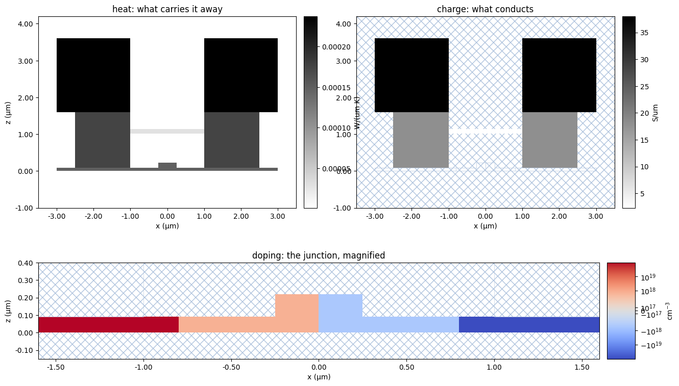
The three panels show the same cross-section read three ways. The heat panel shows the aluminium and tungsten paths that carry heat away from the ring, and the oxide that keeps it there. The electrical panel shows which regions conduct. The doping panel shows the junction inside the core, with the ohmic implants two orders of magnitude higher and set back from it.
Next
Component Library builds the devices on this technology. It draws the ring with its junction and heater, sweeps the coupler gap for the coupling coefficient, runs a charge solve for the index change per volt, and runs a heat solve for the temperature rise per milliwatt. Those measurements turn the drawn ring into a device model the chip-level simulations use.