Key Concepts
Four ideas cover almost everything you will meet in PhotonForge: what a design is (Component), what process it is built in (Technology and PDK), how pieces connect and get measured (Ports), and how physics is attached to them (Models). A fifth, circuit and system simulation, is what those four make possible.
Component
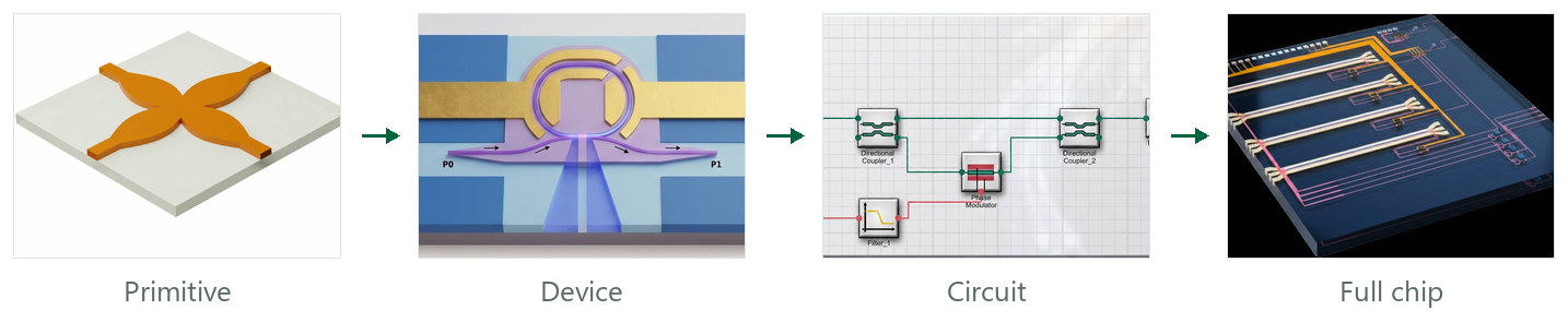
From a single primitive to a full chip: every level is a Component nesting the one before it.
Everything in PhotonForge is a Component, and that is true at every scale.
A single waveguide is a Component, but so is a multi-element circuit and an entire chip.
There is no separate “circuit” or “chip” type: larger systems are simply Components that nest smaller ones.
Components contain all the geometrical and logical structures used to model and simulate the physical device.
Most fabrication processes describe devices with a 2D layout, usually stored as a GDSII or OASIS file, and PhotonForge components are defined by the same 2D geometries to integrate transparently with layout files.
Components are composed hierarchically through Reference instances, so a coupler can sit inside an MZI, inside a transceiver circuit, inside a full reticle, each level reusing the level below.
Two references can point at the same component, so a device used twice is drawn and simulated once.
One Component can also hold several views of the same device. The layout view holds the physical shapes on each process layer. The schematic view holds the symbol and connectivity used to capture a circuit. Both describe the same object, so a change of intent is a change to one Component, not to two files that have to be kept in sync, and the ports and models described below travel with it.
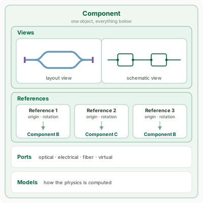
What a Component carries: its views, the references that nest other components, its ports, and the model that computes its physics.
Technology and PDK
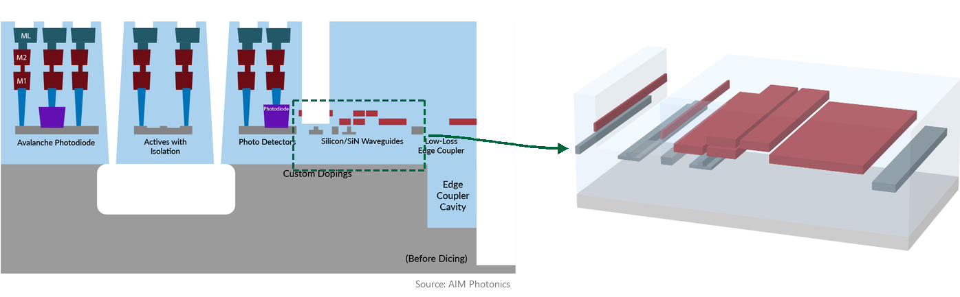
A foundry process cross-section, with the waveguide region extruded into the 3D stack-up a simulation needs. Source: AIM Photonics.
Simulating a device in 3D takes more information than a 2D layout carries: how thick each layer is, what material it is made of, how it is etched. That information comes from the intended fabrication process. Two terms for it are easy to mix up, so it is worth separating them clearly.
Technology = the virtual process.
A Technology holds the layer definitions, the extrusion recipe that turns 2D shapes into a 3D stack-up, and the standard waveguide cross-sections.
Nothing device-specific: this is the process itself, in software.
PDK = technology plus component library. A process design kit bundles that technology stack-up together with a library of ready-made components qualified for the process: couplers, grating couplers, detectors, and so on.
Because PhotonForge is released as a Python module, a PDK is simply another Python package that you install alongside it.
Public PDKs install with pip and expose their technology and component library as importable objects:
PDK |
Package |
|---|---|
SiEPIC OpenEBL, silicon |
|
SiEPIC OpenEBL, silicon nitride |
|
Luxtelligence LNOI400 |
|
Luxtelligence LTOI300 |
|
Proprietary foundry PDKs are distributed by the foundry with their own installation instructions. You can also write a Technology yourself, layer by layer, when you are developing a process rather than consuming one.
See also
Ports
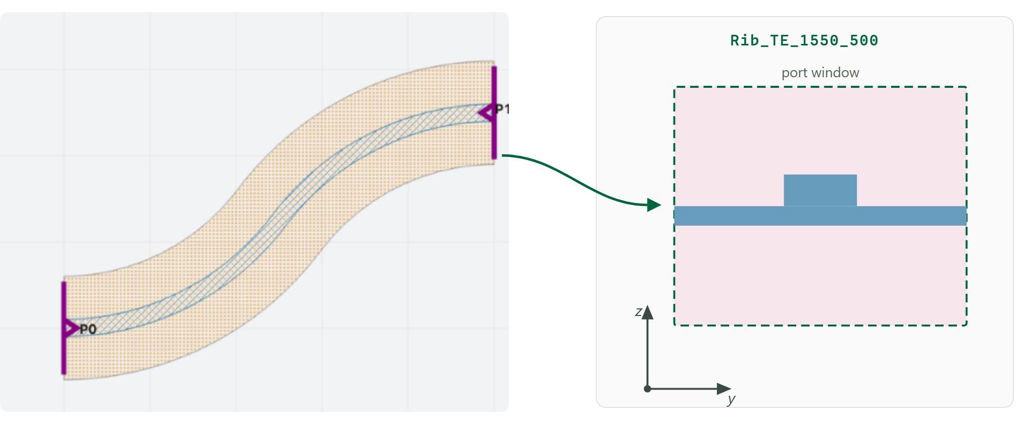
A port marks a terminating cross-section: the waveguide profile at that plane, and the modes it supports.
A Port marks the terminating cross-section of a waveguide, and it does two jobs at once.
In layout, ports are how things connect. Placing one component’s port against another’s aligns and joins them, and the routers build waveguides between ports rather than between coordinates.
In simulation, ports are where signals go in and out. Each port is an excitation and a measurement point, so the set of ports defines the shape of the component’s scattering parameter (S parameter) response.
A PhotonForge port carries more than a pin or a layout marker does.
It knows its cross-section and the modes that cross-section supports, which is what lets the software excite the right mode and check that two connected ports are actually compatible.
Ports also come in several kinds: optical waveguide ports, electrical ports and terminals, fiber ports for off-chip coupling, GaussianPort for free-space beams, and virtual ports (virtual_port_spec()) for models that carry a signal without any geometry to draw.
See also
Models

A model turns a component’s layout and ports into a response, in the frequency domain or in time.
To bridge the layout description of the device to its S parameters, a model is added to the component to perform that computation from the component’s internal structures and ports. Models span a spectrum from instant and ideal to full-wave and exact, and the same component can carry different models as your design matures: prototype with an analytic model, then validate the critical block in FDTD without touching the layout.
Model family |
What it computes |
|---|---|
Analytic models |
Closed-form and instant: |
Circuit model |
|
Tidy3D FDTD |
|
EME, data, and custom |
|
The models are not a black box. The analytic building blocks ship as readable Python inside the package: photonforge.abstract is source you can open, read, and copy from, and the compact model guides walk through the equations one model at a time. So when a built-in model does not describe your device, you are not stuck: start from the closest analytic model, change what your physics requires, and attach the result to any component as a custom model.
See also
S Parameters, Tidy3D Model, Compact Models, Data Model, Custom Model
Circuit and System Simulation
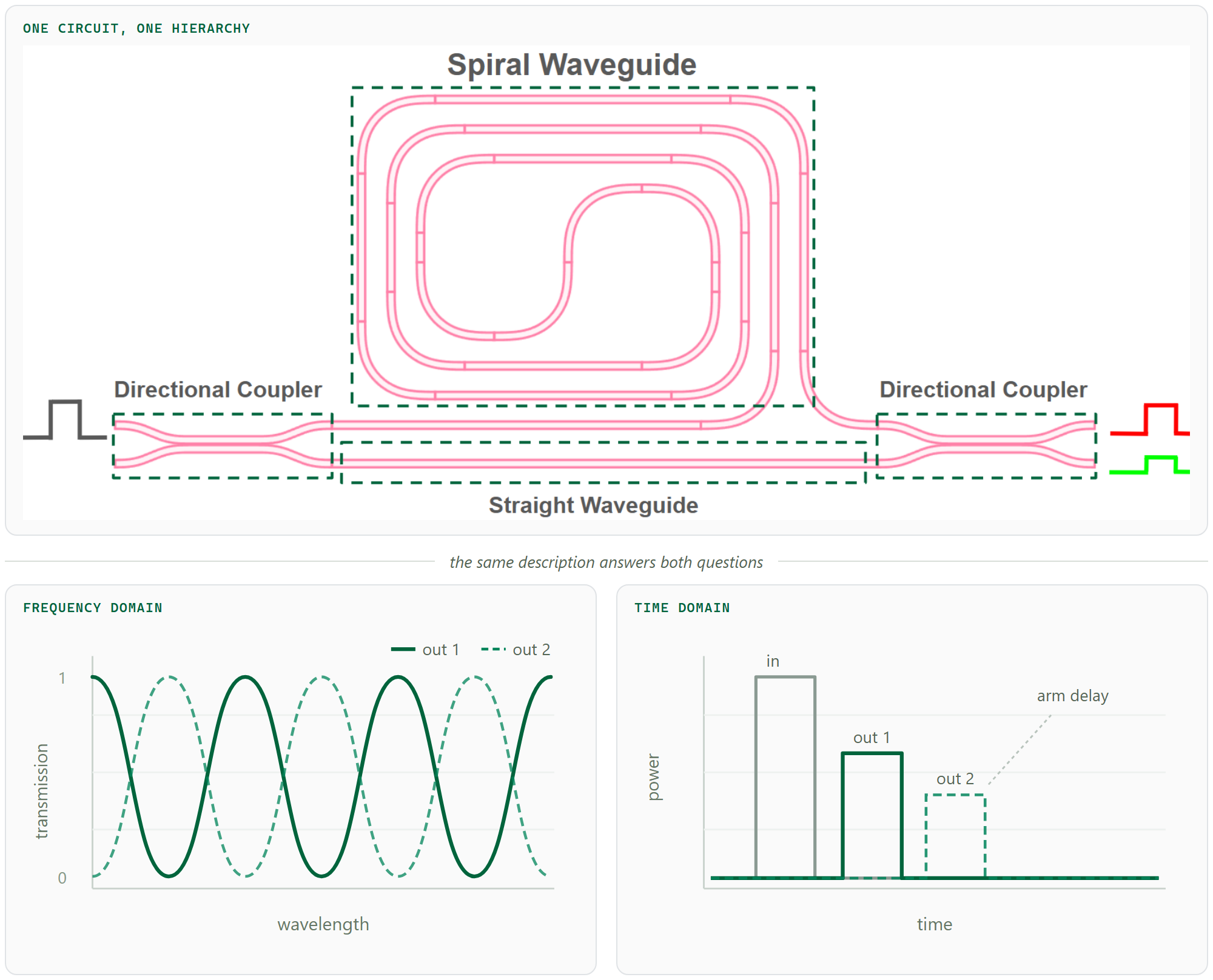
An unbalanced MZI, and the two regimes its single description feeds. Each dashed box is a sub-component with a model of its own.
Because a circuit, and a whole chip, is itself a Component, once its sub-components have models you can simulate the complete system in two complementary regimes.
Regime |
What it produces |
|---|---|
Frequency domain |
|
Time domain |
Time-stepping engines drive lasers, modulators, photodiodes, amplifiers, and noise sources to produce transient signals, eye diagrams, and bit error rates. |
This simulation is layout-aware. You do not hand-build a netlist to go with your layout. PhotonForge walks down the component hierarchy, collects the model attached to each sub-component, and reads the connectivity from how the ports actually meet in the layout. Move a component, reroute a waveguide, or swap an analytic model for an FDTD result, and the next circuit simulation reflects it. The physical design and the system-level prediction cannot drift apart, because there is only one description of the circuit.
See also