

Layout vs. Schematic (LVS)
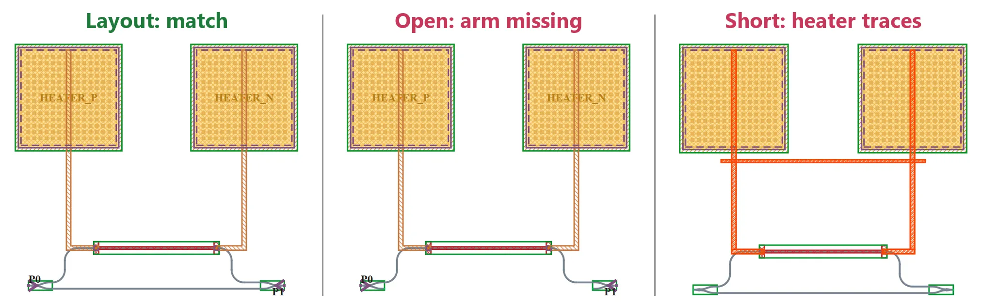
A layout-versus-schematic (LVS) check extracts the connectivity of a layout from its geometry and compares it with the circuit the designer intended, the schematic. It reports nets the layout leaves open, nets the layout joins that should be separate (shorts), and devices connected to the wrong ports.
A photonic chip has two kinds of nets:
- Optical nets are carried by the waveguide core. A waveguide joins the device ports it touches, and two waveguides that cross or overlap join their nets as well, because light can pass from one to the other.
- Electrical nets are carried by the metals and the vias, as on an electronic chip. A heater or a p-n junction is a device between two terminals, so a metal shape that bridges its two ends is a short.
lvs_check runs the comparison in KLayout from three inputs:
- The schematic. PhotonForge writes it as a SPICE netlist from Component.get_netlist: one subcircuit per cell, whose pins are the cell’s ports and terminals. Connections, virtual connections and virtual nets become nets. A route built by the parametric routing functions is written as a wire between its two ends, so a routed component and its unrouted version give the same schematic.
- The pin markers. The exported layout holds shapes only, no ports. The runset finds the pins of each cell from marker boxes and text labels drawn in the layout.
- The runset. A KLayout LVS script, usually part of the PDK, that reads the layers, declares which ones conduct, extracts the nets and runs the comparison.
This guide uses SiPhoPDK, a demonstration PDK for PhotonForge: a synthetic 220 nm silicon-on-insulator process for the O-band, with silicon nitride, germanium photodiodes, a heater and two metal layers. It ships a KLayout LVS runset that extracts both the optical and the electrical nets, and every SiPhoPDK cell draws the markers the runset reads. SiPhoPDK is not a foundry PDK and must not be used for a tape-out.
The guide builds a Mach-Zehnder interferometer (MZI) with a heater in one arm and two bond pads, checks it, then finds a missing waveguide (an open) and a metal bar across the heater traces (a short), and shows where each fault is in the layout. The full API is described in Layout Verification.
Prerequisites
Section titled “Prerequisites”- Install the full KLayout application, version 0.29.12 or newer, from the KLayout download page. PhotonForge searches for it in
PATHand in the common install locations; setpf.config.klayout_executablewhen it is installed elsewhere. - Install SiPhoPDK with
pip install siphopdk-forge. The LVS runset is part of the package, which this guide imports aspdk.
import photonforge as pfimport siphopdk as pdkfrom photonforge.live_viewer import LiveViewer
# Start the LiveViewer to see the layouts in a browserviewer = LiveViewer()
LiveViewer started at http://127.0.0.1:45293. Call its 'stop()' method to free the port.Setting up the technology
Section titled “Setting up the technology”pdk.siphopdk() creates the SiPhoPDK technology. We add one annotation layer, LVS_ERROR, to draw the faulty nets on the layout later. It is not part of the process.
# Create the SiPhoPDK technologytech = pdk.siphopdk()
# Add a layer to highlight faulty nets, outside the layers the runset readstech.add_layer("LVS_ERROR", pf.LayerSpec((99, 0), "Faulty net", "#ff4500cc", "xx"))
# Use the technology for every new componentpf.config.default_technology = tech
The SiPhoPDK cells
Section titled “The SiPhoPDK cells”The MZI uses three SiPhoPDK cells:
y_branch, a 1x2 splitter with portsP0(input),P1andP2(outputs);thermal_phase_shifter, a strip waveguide with a TiN heater, with optical portsP0andP1and heater terminalsHTRPandHTRN;bond_pad, a pad on the second metal with a landing on the first metal, with terminalsM1andT.
Every SiPhoPDK cell draws the markers that the runset reads: its outline on DEVREC, a box on each optical port on PINREC, a box on each electrical terminal on PINREC_E, and the port and terminal names as text. The phase shifter shows all of them:
# Build the three cells with their default parameterssplitter = pdk.component.y_branch()heater = pdk.component.thermal_phase_shifter()pad = pdk.component.bond_pad()
viewer(heater)
Building the MZI
Section titled “Building the MZI”The parametric component below builds the MZI with component_from_netlist. One Y-branch splits the light and a second Y-branch, rotated by 180°, combines it. The upper arm runs through the phase shifter, and each heater terminal is wired to its own bond pad.
The component is built in two forms:
routed=Falsejoins the optical ports with virtual connections and the heater terminals with virtual nets. This is the design intent, the form a schematic editor produces.routed=Truedraws the waveguides with route and the metal traces with route_manhattan. This is the layout.
@pf.parametric_componentdef create_mzi(*, routed=True):    # Place the splitter, the combiner, the phase shifter and the two pads    netlist = {        "name": "MZI",        "instances": {            "split": splitter,            "combine": {"component": splitter, "origin": (200, 0), "rotation": 180},            "heater": {"component": heater, "origin": (50, 30)},            "pad_p": {"component": pad, "origin": (30, 150)},            "pad_n": {"component": pad, "origin": (170, 150)},        },        # Expose the optical input and output, and the top metal of both pads        "ports": [("split", "P0"), ("combine", "P0")],        "terminals": [("pad_p", "T", "HEATER_P"), ("pad_n", "T", "HEATER_N")],    }
    # Optical links: the upper arm through the phase shifter, and the lower arm    optical = [        (("split", "P1"), ("heater", "P0")),        (("heater", "P1"), ("combine", "P2")),        (("split", "P2"), ("combine", "P1")),    ]
    # Electrical links: each heater terminal to the first metal of its pad    electrical = [        (("heater", "HTRP"), ("pad_p", "M1")),        (("heater", "HTRN"), ("pad_n", "M1")),    ]
    if routed:        # Draw the waveguides with a 10 µm bend radius, and the metal traces        netlist["routes"] = [(*link, {"radius": 10}) for link in optical]        netlist["terminal routes"] = electrical    else:        # Declare the same links as intent only        netlist["virtual connections"] = optical        netlist["virtual nets"] = [list(link) for link in electrical]
    return pf.component_from_netlist(netlist)
# Build the design intent and the layoutintent = create_mzi(routed=False)layout = create_mzi()viewer(layout);fill:%23221f20;font-weight:bold;font-size:8.748000px;}.terminal{fill:none;stroke:%23805080;stroke-width:1.093500;}.dashed{stroke-dasharray:5.467500,3.280500;}.port{fill:none;stroke:%23805080;stroke-width:2.187000;}.virtual-connection{fill:none;stroke:%23907090;stroke-width:1.640250;}.layer_100_0{stroke:%23009630;fill:none;}.label_100_0{fill:%23009630;}.layer_81_0{stroke:%23333333;fill:none;}.label_81_0{fill:%23333333;}.layer_70_0{stroke:%237591ab;fill:none;}.label_70_0{fill:%237591ab;}.layer_95_0{stroke:%23ff0000;fill:none;}.label_95_0{fill:%23ff0000;}.layer_91_0{stroke:%23b88018;fill:url(%23pat-layer_91_0);fill-opacity:0.661;}.label_91_0{fill:%23b88018;}.layer_90_0{stroke:%2378838f;fill:url(%23pat-layer_90_0);fill-opacity:0.661;}.label_90_0{fill:%2378838f;}.layer_80_0{stroke:%2300643c;fill:none;}.label_80_0{fill:%2300643c;}.layer_8_0{stroke:%2336a9cc;fill:%2338b0d4;fill-opacity:0.753;}.label_8_0{fill:%2336a9cc;}.layer_3_0{stroke:%237f6833;fill:url(%23pat-layer_3_0);fill-opacity:0.842;}.label_3_0{fill:%237f6833;}.layer_30_0{stroke:%23c0272d;fill:url(%23pat-layer_30_0);fill-opacity:0.918;}.label_30_0{fill:%23c0272d;}.layer_99_0{stroke:%23ff4500;fill:url(%23pat-layer_99_0);fill-opacity:0.935;}.label_99_0{fill:%23ff4500;}.layer_50_0{stroke:%23c6773e;fill:url(%23pat-layer_50_0);fill-opacity:0.895;}.label_50_0{fill:%23c6773e;}.layer_52_0{stroke:%23b88018;fill:url(%23pat-layer_52_0);fill-opacity:0.895;}.label_52_0{fill:%23b88018;}.layer_106_0{stroke:%233355ff;fill:none;}.label_106_0{fill:%233355ff;}.layer_92_0{stroke:%23878787;fill:none;}.label_92_0{fill:%23878787;}.layer_22_0{stroke:%236a975e;fill:url(%23pat-layer_22_0);fill-opacity:0.781;}.label_22_0{fill:%236a975e;}.layer_24_0{stroke:%234f9e42;fill:url(%23pat-layer_24_0);fill-opacity:0.842;}.label_24_0{fill:%234f9e42;}.layer_20_0{stroke:%235f715a;fill:url(%23pat-layer_20_0);fill-opacity:0.781;}.label_20_0{fill:%235f715a;}.layer_60_0{stroke:%237f6833;fill:%23ffd166;fill-opacity:0.690;}.label_60_0{fill:%237f6833;}.layer_101_0{stroke:%2300c853;fill:%2300c853;fill-opacity:0.502;}.label_101_0{fill:%2300c853;}.layer_102_0{stroke:%23e07b00;fill:%23ff8c00;fill-opacity:0.502;}.label_102_0{fill:%23e07b00;}.layer_23_0{stroke:%23c56d87;fill:url(%23pat-layer_23_0);fill-opacity:0.781;}.label_23_0{fill:%23c56d87;}.layer_25_0{stroke:%23c94f74;fill:url(%23pat-layer_25_0);fill-opacity:0.842;}.label_25_0{fill:%23c94f74;}.layer_21_0{stroke:%2385636d;fill:url(%23pat-layer_21_0);fill-opacity:0.781;}.label_21_0{fill:%2385636d;}.layer_1_0{stroke:%2378838f;fill:%2378838f;fill-opacity:0.753;}.label_1_0{fill:%2378838f;}.layer_5_0{stroke:%232f5fd0;fill:%232f5fd0;fill-opacity:0.753;}.label_5_0{fill:%232f5fd0;}.layer_2_0{stroke:%23838c96;fill:url(%23pat-layer_2_0);fill-opacity:0.842;}.label_2_0{fill:%23838c96;}.layer_105_0{stroke:%23202020;fill:none;}.label_105_0{fill:%23202020;}.layer_40_0{stroke:%238a5a2b;fill:%238a5a2b;fill-opacity:0.753;}.label_40_0{fill:%238a5a2b;}.layer_41_0{stroke:%238a5a2b;fill:%238a5a2b;fill-opacity:0.753;}.label_41_0{fill:%238a5a2b;}.layer_42_0{stroke:%23a3652f;fill:%23a3652f;fill-opacity:0.753;}.label_42_0{fill:%23a3652f;}</style><defs><path id=%22port-symbol%22 class=%22port%22 d=%22M 0,-4.374000 L 6.561000,0 0,4.374000%22 /><path id=%22ref-port-symbol%22 class=%22port%22 style=%22stroke-opacity:0.33;%22 d=%22M 0,-3.280500 C 4.374000,-3.280500 4.374000,3.280500 0,3.280500%22 /><circle id=%22port-bend-symbol%22 style=%22stroke-width:0;stroke:none;fill:%23805080;fill-opacity:1;%22 cx=%220%22 cy=%220%22 r=%221.968300%22 /><circle id=%22connection-symbol%22 style=%22stroke-width:0;stroke:none;fill:%23907090;fill-opacity:1;%22 cx=%220%22 cy=%220%22 r=%222.296350%22 /><pattern id=%22pat-layer_91_0%22 patternUnits=%22userSpaceOnUse%22 width=%225.467500%22 height=%225.467500%22 patternTransform=%22translate(2.572941,3.740921)%22><circle cx=%222.733750%22 cy=%222.733750%22 r=%220.546750%22 style=%22stroke:none;fill:%23b88018;fill-opacity:1.0%22 /></pattern><pattern id=%22pat-layer_90_0%22 patternUnits=%22userSpaceOnUse%22 width=%225.467500%22 height=%225.467500%22 patternTransform=%22translate(0.321618,0.575526)%22><circle cx=%222.733750%22 cy=%222.733750%22 r=%220.546750%22 style=%22stroke:none;fill:%2378838f;fill-opacity:1.0%22 /></pattern><pattern id=%22pat-layer_3_0%22 patternUnits=%22userSpaceOnUse%22 width=%223.280500%22 height=%223.280500%22 patternTransform=%22translate(0.771882,2.417211)%22><line x1=%223.280500%22 y1=%220%22 x2=%220%22 y2=%223.280500%22 style=%22stroke:%237f6833;stroke-width:0.546750%22 /><line x1=%224.920750%22 y1=%221.640250%22 x2=%221.640250%22 y2=%224.920750%22 style=%22stroke:%237f6833;stroke-width:0.546750%22 /><line x1=%221.640250%22 y1=%22-1.640250%22 x2=%22-1.640250%22 y2=%221.640250%22 style=%22stroke:%237f6833;stroke-width:0.546750%22 /></pattern><pattern id=%22pat-layer_30_0%22 patternUnits=%22userSpaceOnUse%22 width=%225.467500%22 height=%225.467500%22 patternTransform=%22translate(1.929706,2.014342)%22><line x1=%220%22 y1=%220%22 x2=%225.467500%22 y2=%225.467500%22 style=%22stroke:%23c0272d;stroke-width:0.546750%22 /><line x1=%22-2.733750%22 y1=%222.733750%22 x2=%222.733750%22 y2=%228.201250%22 style=%22stroke:%23c0272d;stroke-width:0.546750%22 /><line x1=%222.733750%22 y1=%22-2.733750%22 x2=%228.201250%22 y2=%222.733750%22 style=%22stroke:%23c0272d;stroke-width:0.546750%22 /><line x1=%225.467500%22 y1=%220%22 x2=%220%22 y2=%225.467500%22 style=%22stroke:%23c0272d;stroke-width:0.546750%22 /><line x1=%228.201250%22 y1=%222.733750%22 x2=%222.733750%22 y2=%228.201250%22 style=%22stroke:%23c0272d;stroke-width:0.546750%22 /><line x1=%222.733750%22 y1=%22-2.733750%22 x2=%22-2.733750%22 y2=%222.733750%22 style=%22stroke:%23c0272d;stroke-width:0.546750%22 /></pattern><pattern id=%22pat-layer_99_0%22 patternUnits=%22userSpaceOnUse%22 width=%223.280500%22 height=%223.280500%22 patternTransform=%22translate(2.508618,1.035947)%22><line x1=%220%22 y1=%220%22 x2=%223.280500%22 y2=%223.280500%22 style=%22stroke:%23ff4500;stroke-width:0.546750%22 /><line x1=%22-1.640250%22 y1=%221.640250%22 x2=%221.640250%22 y2=%224.920750%22 style=%22stroke:%23ff4500;stroke-width:0.546750%22 /><line x1=%221.640250%22 y1=%22-1.640250%22 x2=%224.920750%22 y2=%221.640250%22 style=%22stroke:%23ff4500;stroke-width:0.546750%22 /><line x1=%223.280500%22 y1=%220%22 x2=%220%22 y2=%223.280500%22 style=%22stroke:%23ff4500;stroke-width:0.546750%22 /><line x1=%224.920750%22 y1=%221.640250%22 x2=%221.640250%22 y2=%224.920750%22 style=%22stroke:%23ff4500;stroke-width:0.546750%22 /><line x1=%221.640250%22 y1=%22-1.640250%22 x2=%22-1.640250%22 y2=%221.640250%22 style=%22stroke:%23ff4500;stroke-width:0.546750%22 /></pattern><pattern id=%22pat-layer_50_0%22 patternUnits=%22userSpaceOnUse%22 width=%223.280500%22 height=%223.280500%22 patternTransform=%22translate(1.929706,3.107842)%22><line x1=%223.280500%22 y1=%220%22 x2=%220%22 y2=%223.280500%22 style=%22stroke:%23c6773e;stroke-width:0.546750%22 /><line x1=%224.920750%22 y1=%221.640250%22 x2=%221.640250%22 y2=%224.920750%22 style=%22stroke:%23c6773e;stroke-width:0.546750%22 /><line x1=%221.640250%22 y1=%22-1.640250%22 x2=%22-1.640250%22 y2=%221.640250%22 style=%22stroke:%23c6773e;stroke-width:0.546750%22 /></pattern><pattern id=%22pat-layer_52_0%22 patternUnits=%22userSpaceOnUse%22 width=%223.280500%22 height=%223.280500%22 patternTransform=%22translate(1.350794,0.345316)%22><line x1=%220%22 y1=%220%22 x2=%223.280500%22 y2=%223.280500%22 style=%22stroke:%23b88018;stroke-width:0.546750%22 /><line x1=%22-1.640250%22 y1=%221.640250%22 x2=%221.640250%22 y2=%224.920750%22 style=%22stroke:%23b88018;stroke-width:0.546750%22 /><line x1=%221.640250%22 y1=%22-1.640250%22 x2=%224.920750%22 y2=%221.640250%22 style=%22stroke:%23b88018;stroke-width:0.546750%22 /></pattern><pattern id=%22pat-layer_22_0%22 patternUnits=%22userSpaceOnUse%22 width=%223.280500%22 height=%223.280500%22 patternTransform=%22translate(0.192971,2.417211)%22><circle cx=%221.640250%22 cy=%221.640250%22 r=%220.546750%22 style=%22stroke:none;fill:%236a975e;fill-opacity:1.0%22 /></pattern><pattern id=%22pat-layer_24_0%22 patternUnits=%22userSpaceOnUse%22 width=%223.280500%22 height=%223.280500%22 patternTransform=%22translate(2.894559,2.935184)%22><line x1=%220%22 y1=%220%22 x2=%223.280500%22 y2=%223.280500%22 style=%22stroke:%234f9e42;stroke-width:0.546750%22 /><line x1=%22-1.640250%22 y1=%221.640250%22 x2=%221.640250%22 y2=%224.920750%22 style=%22stroke:%234f9e42;stroke-width:0.546750%22 /><line x1=%221.640250%22 y1=%22-1.640250%22 x2=%224.920750%22 y2=%221.640250%22 style=%22stroke:%234f9e42;stroke-width:0.546750%22 /><line x1=%223.280500%22 y1=%220%22 x2=%220%22 y2=%223.280500%22 style=%22stroke:%234f9e42;stroke-width:0.546750%22 /><line x1=%224.920750%22 y1=%221.640250%22 x2=%221.640250%22 y2=%224.920750%22 style=%22stroke:%234f9e42;stroke-width:0.546750%22 /><line x1=%221.640250%22 y1=%22-1.640250%22 x2=%22-1.640250%22 y2=%221.640250%22 style=%22stroke:%234f9e42;stroke-width:0.546750%22 /></pattern><pattern id=%22pat-layer_20_0%22 patternUnits=%22userSpaceOnUse%22 width=%225.467500%22 height=%225.467500%22 patternTransform=%22translate(1.286471,3.165395)%22><circle cx=%222.733750%22 cy=%222.733750%22 r=%220.546750%22 style=%22stroke:none;fill:%235f715a;fill-opacity:1.0%22 /></pattern><pattern id=%22pat-layer_23_0%22 patternUnits=%22userSpaceOnUse%22 width=%223.280500%22 height=%223.280500%22 patternTransform=%22translate(1.543765,1.035947)%22><circle cx=%221.640250%22 cy=%221.640250%22 r=%220.546750%22 style=%22stroke:none;fill:%23c56d87;fill-opacity:1.0%22 /></pattern><pattern id=%22pat-layer_25_0%22 patternUnits=%22userSpaceOnUse%22 width=%223.280500%22 height=%223.280500%22 patternTransform=%22translate(0.964853,1.553921)%22><line x1=%220%22 y1=%220%22 x2=%223.280500%22 y2=%223.280500%22 style=%22stroke:%23c94f74;stroke-width:0.546750%22 /><line x1=%22-1.640250%22 y1=%221.640250%22 x2=%221.640250%22 y2=%224.920750%22 style=%22stroke:%23c94f74;stroke-width:0.546750%22 /><line x1=%221.640250%22 y1=%22-1.640250%22 x2=%224.920750%22 y2=%221.640250%22 style=%22stroke:%23c94f74;stroke-width:0.546750%22 /><line x1=%223.280500%22 y1=%220%22 x2=%220%22 y2=%223.280500%22 style=%22stroke:%23c94f74;stroke-width:0.546750%22 /><line x1=%224.920750%22 y1=%221.640250%22 x2=%221.640250%22 y2=%224.920750%22 style=%22stroke:%23c94f74;stroke-width:0.546750%22 /><line x1=%221.640250%22 y1=%22-1.640250%22 x2=%22-1.640250%22 y2=%221.640250%22 style=%22stroke:%23c94f74;stroke-width:0.546750%22 /></pattern><pattern id=%22pat-layer_21_0%22 patternUnits=%22userSpaceOnUse%22 width=%225.467500%22 height=%225.467500%22 patternTransform=%22translate(3.537794,0.863289)%22><circle cx=%222.733750%22 cy=%222.733750%22 r=%220.546750%22 style=%22stroke:none;fill:%2385636d;fill-opacity:1.0%22 /></pattern><pattern id=%22pat-layer_2_0%22 patternUnits=%22userSpaceOnUse%22 width=%223.280500%22 height=%223.280500%22 patternTransform=%22translate(2.701588,0.517974)%22><line x1=%220%22 y1=%220%22 x2=%223.280500%22 y2=%223.280500%22 style=%22stroke:%23838c96;stroke-width:0.546750%22 /><line x1=%22-1.640250%22 y1=%221.640250%22 x2=%221.640250%22 y2=%224.920750%22 style=%22stroke:%23838c96;stroke-width:0.546750%22 /><line x1=%221.640250%22 y1=%22-1.640250%22 x2=%224.920750%22 y2=%221.640250%22 style=%22stroke:%23838c96;stroke-width:0.546750%22 /></pattern><g id=%22C1%22 data-name=%22ybranch%22><path class=%22layer_1_0%22 d=%22M -2.000000,-0.200000 0.000000,-0.200000 1.500000,-0.450000 3.000000,-0.700000 3.000000,0.700000 1.500000,0.450000 0.000000,0.200000 -2.000000,0.200000 z%22 /><path class=%22layer_1_0%22 d=%22M 3.000000,0.150000 3.771000,0.155000 4.159000,0.167000 4.935000,0.222000 5.322000,0.265000 6.091000,0.382000 6.852000,0.540000 7.604000,0.737000 7.976000,0.851000 8.709000,1.105000 9.069000,1.237000 9.787000,1.498000 10.508000,1.729000 10.872000,1.830000 11.239000,1.921000 11.980000,2.074000 12.353000,2.136000 12.728000,2.188000 13.481000,2.261000 13.858000,2.283000 14.617000,2.299000 15.000000,2.300000 17.000000,2.300000 17.000000,2.700000 15.000000,2.700000 14.422000,2.698000 13.841000,2.683000 13.065000,2.628000 12.678000,2.585000 11.909000,2.468000 11.148000,2.310000 10.396000,2.113000 10.024000,1.999000 9.656000,1.875000 8.931000,1.613000 8.213000,1.352000 7.492000,1.121000 7.128000,1.020000 6.761000,0.929000 6.020000,0.776000 5.647000,0.714000 5.272000,0.662000 4.896000,0.621000 4.142000,0.567000 3.763000,0.555000 3.000000,0.550000 z%22 /><path class=%22layer_1_0%22 d=%22M 3.000000,-0.550000 3.763000,-0.555000 4.142000,-0.567000 4.896000,-0.621000 5.272000,-0.662000 5.647000,-0.714000 6.020000,-0.776000 6.761000,-0.929000 7.128000,-1.020000 7.492000,-1.121000 8.213000,-1.352000 8.931000,-1.613000 9.656000,-1.875000 10.024000,-1.999000 10.396000,-2.113000 11.148000,-2.310000 11.909000,-2.468000 12.678000,-2.585000 13.065000,-2.628000 13.841000,-2.683000 14.422000,-2.698000 15.000000,-2.700000 17.000000,-2.700000 17.000000,-2.300000 15.000000,-2.300000 14.617000,-2.299000 13.858000,-2.283000 13.481000,-2.261000 12.728000,-2.188000 12.353000,-2.136000 11.980000,-2.074000 11.239000,-1.921000 10.872000,-1.830000 10.508000,-1.729000 9.787000,-1.498000 9.069000,-1.237000 8.709000,-1.105000 7.976000,-0.851000 7.604000,-0.737000 6.852000,-0.540000 6.091000,-0.382000 5.322000,-0.265000 4.935000,-0.222000 4.159000,-0.167000 3.771000,-0.155000 3.000000,-0.150000 z%22 /><rect class=%22layer_100_0%22 x=%22-2.000000%22 y=%22-3.700000%22 width=%2219.000000%22 height=%227.400000%22 /><rect class=%22layer_101_0%22 x=%22-2.100000%22 y=%22-0.100000%22 width=%220.200000%22 height=%220.200000%22 /><rect class=%22layer_101_0%22 x=%2216.900000%22 y=%222.400000%22 width=%220.200000%22 height=%220.200000%22 /><rect class=%22layer_101_0%22 x=%2216.900000%22 y=%22-2.600000%22 width=%220.200000%22 height=%220.200000%22 /></g><g id=%22C2%22 data-name=%22tps_l100p0%22><rect class=%22layer_1_0%22 x=%220.000000%22 y=%22-0.200000%22 width=%22100.000000%22 height=%220.400000%22 /><rect class=%22layer_30_0%22 x=%220.000000%22 y=%22-1.000000%22 width=%22100.000000%22 height=%222.000000%22 /><rect class=%22layer_30_0%22 x=%220.000000%22 y=%22-5.000000%22 width=%224.000000%22 height=%2210.000000%22 /><rect class=%22layer_30_0%22 x=%2296.000000%22 y=%22-5.000000%22 width=%224.000000%22 height=%2210.000000%22 /><rect class=%22layer_41_0%22 x=%221.800000%22 y=%22-0.200000%22 width=%220.400000%22 height=%220.400000%22 /><rect class=%22layer_41_0%22 x=%2297.800000%22 y=%22-0.200000%22 width=%220.400000%22 height=%220.400000%22 /><rect class=%22layer_50_0%22 x=%220.250000%22 y=%22-1.750000%22 width=%223.500000%22 height=%223.500000%22 /><rect class=%22layer_50_0%22 x=%2296.250000%22 y=%22-1.750000%22 width=%223.500000%22 height=%223.500000%22 /><rect class=%22layer_100_0%22 x=%220.000000%22 y=%22-5.000000%22 width=%22100.000000%22 height=%2210.000000%22 /><rect class=%22layer_101_0%22 x=%22-0.100000%22 y=%22-0.100000%22 width=%220.200000%22 height=%220.200000%22 /><rect class=%22layer_101_0%22 x=%2299.900000%22 y=%22-0.100000%22 width=%220.200000%22 height=%220.200000%22 /><rect class=%22layer_102_0%22 x=%2297.900000%22 y=%22-0.100000%22 width=%220.200000%22 height=%220.200000%22 /><rect class=%22layer_102_0%22 x=%221.900000%22 y=%22-0.100000%22 width=%220.200000%22 height=%220.200000%22 /><rect class=%22terminal dashed%22 x=%2296.250000%22 y=%22-1.750000%22 width=%223.500000%22 height=%223.500000%22 /><rect class=%22terminal dashed%22 x=%220.250000%22 y=%22-1.750000%22 width=%223.500000%22 height=%223.500000%22 /></g><g id=%22C3%22 data-name=%22pad_s80p0%22><rect class=%22layer_42_0%22 x=%22-33.500000%22 y=%22-33.500000%22 width=%222.000000%22 height=%222.000000%22 /><rect class=%22layer_42_0%22 x=%22-33.500000%22 y=%22-28.500000%22 width=%222.000000%22 height=%222.000000%22 /><rect class=%22layer_42_0%22 x=%22-33.500000%22 y=%22-23.500000%22 width=%222.000000%22 height=%222.000000%22 /><rect class=%22layer_42_0%22 x=%22-33.500000%22 y=%22-18.500000%22 width=%222.000000%22 height=%222.000000%22 /><rect class=%22layer_42_0%22 x=%22-33.500000%22 y=%22-13.500000%22 width=%222.000000%22 height=%222.000000%22 /><rect class=%22layer_42_0%22 x=%22-33.500000%22 y=%22-8.500000%22 width=%222.000000%22 height=%222.000000%22 /><rect class=%22layer_42_0%22 x=%22-33.500000%22 y=%22-3.500000%22 width=%222.000000%22 height=%222.000000%22 /><rect class=%22layer_42_0%22 x=%22-33.500000%22 y=%221.500000%22 width=%222.000000%22 height=%222.000000%22 /><rect class=%22layer_42_0%22 x=%22-33.500000%22 y=%226.500000%22 width=%222.000000%22 height=%222.000000%22 /><rect class=%22layer_42_0%22 x=%22-33.500000%22 y=%2211.500000%22 width=%222.000000%22 height=%222.000000%22 /><rect class=%22layer_42_0%22 x=%22-33.500000%22 y=%2216.500000%22 width=%222.000000%22 height=%222.000000%22 /><rect class=%22layer_42_0%22 x=%22-33.500000%22 y=%2221.500000%22 width=%222.000000%22 height=%222.000000%22 /><rect class=%22layer_42_0%22 x=%22-33.500000%22 y=%2226.500000%22 width=%222.000000%22 height=%222.000000%22 /><rect class=%22layer_42_0%22 x=%22-33.500000%22 y=%2231.500000%22 width=%222.000000%22 height=%222.000000%22 /><rect class=%22layer_42_0%22 x=%22-28.500000%22 y=%22-33.500000%22 width=%222.000000%22 height=%222.000000%22 /><rect class=%22layer_42_0%22 x=%22-28.500000%22 y=%22-28.500000%22 width=%222.000000%22 height=%222.000000%22 /><rect class=%22layer_42_0%22 x=%22-28.500000%22 y=%22-23.500000%22 width=%222.000000%22 height=%222.000000%22 /><rect class=%22layer_42_0%22 x=%22-28.500000%22 y=%22-18.500000%22 width=%222.000000%22 height=%222.000000%22 /><rect class=%22layer_42_0%22 x=%22-28.500000%22 y=%22-13.500000%22 width=%222.000000%22 height=%222.000000%22 /><rect class=%22layer_42_0%22 x=%22-28.500000%22 y=%22-8.500000%22 width=%222.000000%22 height=%222.000000%22 /><rect class=%22layer_42_0%22 x=%22-28.500000%22 y=%22-3.500000%22 width=%222.000000%22 height=%222.000000%22 /><rect class=%22layer_42_0%22 x=%22-28.500000%22 y=%221.500000%22 width=%222.000000%22 height=%222.000000%22 /><rect class=%22layer_42_0%22 x=%22-28.500000%22 y=%226.500000%22 width=%222.000000%22 height=%222.000000%22 /><rect class=%22layer_42_0%22 x=%22-28.500000%22 y=%2211.500000%22 width=%222.000000%22 height=%222.000000%22 /><rect class=%22layer_42_0%22 x=%22-28.500000%22 y=%2216.500000%22 width=%222.000000%22 height=%222.000000%22 /><rect class=%22layer_42_0%22 x=%22-28.500000%22 y=%2221.500000%22 width=%222.000000%22 height=%222.000000%22 /><rect class=%22layer_42_0%22 x=%22-28.500000%22 y=%2226.500000%22 width=%222.000000%22 height=%222.000000%22 /><rect class=%22layer_42_0%22 x=%22-28.500000%22 y=%2231.500000%22 width=%222.000000%22 height=%222.000000%22 /><rect class=%22layer_42_0%22 x=%22-23.500000%22 y=%22-33.500000%22 width=%222.000000%22 height=%222.000000%22 /><rect class=%22layer_42_0%22 x=%22-23.500000%22 y=%22-28.500000%22 width=%222.000000%22 height=%222.000000%22 /><rect class=%22layer_42_0%22 x=%22-23.500000%22 y=%22-23.500000%22 width=%222.000000%22 height=%222.000000%22 /><rect class=%22layer_42_0%22 x=%22-23.500000%22 y=%22-18.500000%22 width=%222.000000%22 height=%222.000000%22 /><rect class=%22layer_42_0%22 x=%22-23.500000%22 y=%22-13.500000%22 width=%222.000000%22 height=%222.000000%22 /><rect class=%22layer_42_0%22 x=%22-23.500000%22 y=%22-8.500000%22 width=%222.000000%22 height=%222.000000%22 /><rect class=%22layer_42_0%22 x=%22-23.500000%22 y=%22-3.500000%22 width=%222.000000%22 height=%222.000000%22 /><rect class=%22layer_42_0%22 x=%22-23.500000%22 y=%221.500000%22 width=%222.000000%22 height=%222.000000%22 /><rect class=%22layer_42_0%22 x=%22-23.500000%22 y=%226.500000%22 width=%222.000000%22 height=%222.000000%22 /><rect class=%22layer_42_0%22 x=%22-23.500000%22 y=%2211.500000%22 width=%222.000000%22 height=%222.000000%22 /><rect class=%22layer_42_0%22 x=%22-23.500000%22 y=%2216.500000%22 width=%222.000000%22 height=%222.000000%22 /><rect class=%22layer_42_0%22 x=%22-23.500000%22 y=%2221.500000%22 width=%222.000000%22 height=%222.000000%22 /><rect class=%22layer_42_0%22 x=%22-23.500000%22 y=%2226.500000%22 width=%222.000000%22 height=%222.000000%22 /><rect class=%22layer_42_0%22 x=%22-23.500000%22 y=%2231.500000%22 width=%222.000000%22 height=%222.000000%22 /><rect class=%22layer_42_0%22 x=%22-18.500000%22 y=%22-33.500000%22 width=%222.000000%22 height=%222.000000%22 /><rect class=%22layer_42_0%22 x=%22-18.500000%22 y=%22-28.500000%22 width=%222.000000%22 height=%222.000000%22 /><rect class=%22layer_42_0%22 x=%22-18.500000%22 y=%22-23.500000%22 width=%222.000000%22 height=%222.000000%22 /><rect class=%22layer_42_0%22 x=%22-18.500000%22 y=%22-18.500000%22 width=%222.000000%22 height=%222.000000%22 /><rect class=%22layer_42_0%22 x=%22-18.500000%22 y=%22-13.500000%22 width=%222.000000%22 height=%222.000000%22 /><rect class=%22layer_42_0%22 x=%22-18.500000%22 y=%22-8.500000%22 width=%222.000000%22 height=%222.000000%22 /><rect class=%22layer_42_0%22 x=%22-18.500000%22 y=%22-3.500000%22 width=%222.000000%22 height=%222.000000%22 /><rect class=%22layer_42_0%22 x=%22-18.500000%22 y=%221.500000%22 width=%222.000000%22 height=%222.000000%22 /><rect class=%22layer_42_0%22 x=%22-18.500000%22 y=%226.500000%22 width=%222.000000%22 height=%222.000000%22 /><rect class=%22layer_42_0%22 x=%22-18.500000%22 y=%2211.500000%22 width=%222.000000%22 height=%222.000000%22 /><rect class=%22layer_42_0%22 x=%22-18.500000%22 y=%2216.500000%22 width=%222.000000%22 height=%222.000000%22 /><rect class=%22layer_42_0%22 x=%22-18.500000%22 y=%2221.500000%22 width=%222.000000%22 height=%222.000000%22 /><rect class=%22layer_42_0%22 x=%22-18.500000%22 y=%2226.500000%22 width=%222.000000%22 height=%222.000000%22 /><rect class=%22layer_42_0%22 x=%22-18.500000%22 y=%2231.500000%22 width=%222.000000%22 height=%222.000000%22 /><rect class=%22layer_42_0%22 x=%22-13.500000%22 y=%22-33.500000%22 width=%222.000000%22 height=%222.000000%22 /><rect class=%22layer_42_0%22 x=%22-13.500000%22 y=%22-28.500000%22 width=%222.000000%22 height=%222.000000%22 /><rect class=%22layer_42_0%22 x=%22-13.500000%22 y=%22-23.500000%22 width=%222.000000%22 height=%222.000000%22 /><rect class=%22layer_42_0%22 x=%22-13.500000%22 y=%22-18.500000%22 width=%222.000000%22 height=%222.000000%22 /><rect class=%22layer_42_0%22 x=%22-13.500000%22 y=%22-13.500000%22 width=%222.000000%22 height=%222.000000%22 /><rect class=%22layer_42_0%22 x=%22-13.500000%22 y=%22-8.500000%22 width=%222.000000%22 height=%222.000000%22 /><rect class=%22layer_42_0%22 x=%22-13.500000%22 y=%22-3.500000%22 width=%222.000000%22 height=%222.000000%22 /><rect class=%22layer_42_0%22 x=%22-13.500000%22 y=%221.500000%22 width=%222.000000%22 height=%222.000000%22 /><rect class=%22layer_42_0%22 x=%22-13.500000%22 y=%226.500000%22 width=%222.000000%22 height=%222.000000%22 /><rect class=%22layer_42_0%22 x=%22-13.500000%22 y=%2211.500000%22 width=%222.000000%22 height=%222.000000%22 /><rect class=%22layer_42_0%22 x=%22-13.500000%22 y=%2216.500000%22 width=%222.000000%22 height=%222.000000%22 /><rect class=%22layer_42_0%22 x=%22-13.500000%22 y=%2221.500000%22 width=%222.000000%22 height=%222.000000%22 /><rect class=%22layer_42_0%22 x=%22-13.500000%22 y=%2226.500000%22 width=%222.000000%22 height=%222.000000%22 /><rect class=%22layer_42_0%22 x=%22-13.500000%22 y=%2231.500000%22 width=%222.000000%22 height=%222.000000%22 /><rect class=%22layer_42_0%22 x=%22-8.500000%22 y=%22-33.500000%22 width=%222.000000%22 height=%222.000000%22 /><rect class=%22layer_42_0%22 x=%22-8.500000%22 y=%22-28.500000%22 width=%222.000000%22 height=%222.000000%22 /><rect class=%22layer_42_0%22 x=%22-8.500000%22 y=%22-23.500000%22 width=%222.000000%22 height=%222.000000%22 /><rect class=%22layer_42_0%22 x=%22-8.500000%22 y=%22-18.500000%22 width=%222.000000%22 height=%222.000000%22 /><rect class=%22layer_42_0%22 x=%22-8.500000%22 y=%22-13.500000%22 width=%222.000000%22 height=%222.000000%22 /><rect class=%22layer_42_0%22 x=%22-8.500000%22 y=%22-8.500000%22 width=%222.000000%22 height=%222.000000%22 /><rect class=%22layer_42_0%22 x=%22-8.500000%22 y=%22-3.500000%22 width=%222.000000%22 height=%222.000000%22 /><rect class=%22layer_42_0%22 x=%22-8.500000%22 y=%221.500000%22 width=%222.000000%22 height=%222.000000%22 /><rect class=%22layer_42_0%22 x=%22-8.500000%22 y=%226.500000%22 width=%222.000000%22 height=%222.000000%22 /><rect class=%22layer_42_0%22 x=%22-8.500000%22 y=%2211.500000%22 width=%222.000000%22 height=%222.000000%22 /><rect class=%22layer_42_0%22 x=%22-8.500000%22 y=%2216.500000%22 width=%222.000000%22 height=%222.000000%22 /><rect class=%22layer_42_0%22 x=%22-8.500000%22 y=%2221.500000%22 width=%222.000000%22 height=%222.000000%22 /><rect class=%22layer_42_0%22 x=%22-8.500000%22 y=%2226.500000%22 width=%222.000000%22 height=%222.000000%22 /><rect class=%22layer_42_0%22 x=%22-8.500000%22 y=%2231.500000%22 width=%222.000000%22 height=%222.000000%22 /><rect class=%22layer_42_0%22 x=%22-3.500000%22 y=%22-33.500000%22 width=%222.000000%22 height=%222.000000%22 /><rect class=%22layer_42_0%22 x=%22-3.500000%22 y=%22-28.500000%22 width=%222.000000%22 height=%222.000000%22 /><rect class=%22layer_42_0%22 x=%22-3.500000%22 y=%22-23.500000%22 width=%222.000000%22 height=%222.000000%22 /><rect class=%22layer_42_0%22 x=%22-3.500000%22 y=%22-18.500000%22 width=%222.000000%22 height=%222.000000%22 /><rect class=%22layer_42_0%22 x=%22-3.500000%22 y=%22-13.500000%22 width=%222.000000%22 height=%222.000000%22 /><rect class=%22layer_42_0%22 x=%22-3.500000%22 y=%22-8.500000%22 width=%222.000000%22 height=%222.000000%22 /><rect class=%22layer_42_0%22 x=%22-3.500000%22 y=%22-3.500000%22 width=%222.000000%22 height=%222.000000%22 /><rect class=%22layer_42_0%22 x=%22-3.500000%22 y=%221.500000%22 width=%222.000000%22 height=%222.000000%22 /><rect class=%22layer_42_0%22 x=%22-3.500000%22 y=%226.500000%22 width=%222.000000%22 height=%222.000000%22 /><rect class=%22layer_42_0%22 x=%22-3.500000%22 y=%2211.500000%22 width=%222.000000%22 height=%222.000000%22 /><rect class=%22layer_42_0%22 x=%22-3.500000%22 y=%2216.500000%22 width=%222.000000%22 height=%222.000000%22 /><rect class=%22layer_42_0%22 x=%22-3.500000%22 y=%2221.500000%22 width=%222.000000%22 height=%222.000000%22 /><rect class=%22layer_42_0%22 x=%22-3.500000%22 y=%2226.500000%22 width=%222.000000%22 height=%222.000000%22 /><rect class=%22layer_42_0%22 x=%22-3.500000%22 y=%2231.500000%22 width=%222.000000%22 height=%222.000000%22 /><rect class=%22layer_42_0%22 x=%221.500000%22 y=%22-33.500000%22 width=%222.000000%22 height=%222.000000%22 /><rect class=%22layer_42_0%22 x=%221.500000%22 y=%22-28.500000%22 width=%222.000000%22 height=%222.000000%22 /><rect class=%22layer_42_0%22 x=%221.500000%22 y=%22-23.500000%22 width=%222.000000%22 height=%222.000000%22 /><rect class=%22layer_42_0%22 x=%221.500000%22 y=%22-18.500000%22 width=%222.000000%22 height=%222.000000%22 /><rect class=%22layer_42_0%22 x=%221.500000%22 y=%22-13.500000%22 width=%222.000000%22 height=%222.000000%22 /><rect class=%22layer_42_0%22 x=%221.500000%22 y=%22-8.500000%22 width=%222.000000%22 height=%222.000000%22 /><rect class=%22layer_42_0%22 x=%221.500000%22 y=%22-3.500000%22 width=%222.000000%22 height=%222.000000%22 /><rect class=%22layer_42_0%22 x=%221.500000%22 y=%221.500000%22 width=%222.000000%22 height=%222.000000%22 /><rect class=%22layer_42_0%22 x=%221.500000%22 y=%226.500000%22 width=%222.000000%22 height=%222.000000%22 /><rect class=%22layer_42_0%22 x=%221.500000%22 y=%2211.500000%22 width=%222.000000%22 height=%222.000000%22 /><rect class=%22layer_42_0%22 x=%221.500000%22 y=%2216.500000%22 width=%222.000000%22 height=%222.000000%22 /><rect class=%22layer_42_0%22 x=%221.500000%22 y=%2221.500000%22 width=%222.000000%22 height=%222.000000%22 /><rect class=%22layer_42_0%22 x=%221.500000%22 y=%2226.500000%22 width=%222.000000%22 height=%222.000000%22 /><rect class=%22layer_42_0%22 x=%221.500000%22 y=%2231.500000%22 width=%222.000000%22 height=%222.000000%22 /><rect class=%22layer_42_0%22 x=%226.500000%22 y=%22-33.500000%22 width=%222.000000%22 height=%222.000000%22 /><rect class=%22layer_42_0%22 x=%226.500000%22 y=%22-28.500000%22 width=%222.000000%22 height=%222.000000%22 /><rect class=%22layer_42_0%22 x=%226.500000%22 y=%22-23.500000%22 width=%222.000000%22 height=%222.000000%22 /><rect class=%22layer_42_0%22 x=%226.500000%22 y=%22-18.500000%22 width=%222.000000%22 height=%222.000000%22 /><rect class=%22layer_42_0%22 x=%226.500000%22 y=%22-13.500000%22 width=%222.000000%22 height=%222.000000%22 /><rect class=%22layer_42_0%22 x=%226.500000%22 y=%22-8.500000%22 width=%222.000000%22 height=%222.000000%22 /><rect class=%22layer_42_0%22 x=%226.500000%22 y=%22-3.500000%22 width=%222.000000%22 height=%222.000000%22 /><rect class=%22layer_42_0%22 x=%226.500000%22 y=%221.500000%22 width=%222.000000%22 height=%222.000000%22 /><rect class=%22layer_42_0%22 x=%226.500000%22 y=%226.500000%22 width=%222.000000%22 height=%222.000000%22 /><rect class=%22layer_42_0%22 x=%226.500000%22 y=%2211.500000%22 width=%222.000000%22 height=%222.000000%22 /><rect class=%22layer_42_0%22 x=%226.500000%22 y=%2216.500000%22 width=%222.000000%22 height=%222.000000%22 /><rect class=%22layer_42_0%22 x=%226.500000%22 y=%2221.500000%22 width=%222.000000%22 height=%222.000000%22 /><rect class=%22layer_42_0%22 x=%226.500000%22 y=%2226.500000%22 width=%222.000000%22 height=%222.000000%22 /><rect class=%22layer_42_0%22 x=%226.500000%22 y=%2231.500000%22 width=%222.000000%22 height=%222.000000%22 /><rect class=%22layer_42_0%22 x=%2211.500000%22 y=%22-33.500000%22 width=%222.000000%22 height=%222.000000%22 /><rect class=%22layer_42_0%22 x=%2211.500000%22 y=%22-28.500000%22 width=%222.000000%22 height=%222.000000%22 /><rect class=%22layer_42_0%22 x=%2211.500000%22 y=%22-23.500000%22 width=%222.000000%22 height=%222.000000%22 /><rect class=%22layer_42_0%22 x=%2211.500000%22 y=%22-18.500000%22 width=%222.000000%22 height=%222.000000%22 /><rect class=%22layer_42_0%22 x=%2211.500000%22 y=%22-13.500000%22 width=%222.000000%22 height=%222.000000%22 /><rect class=%22layer_42_0%22 x=%2211.500000%22 y=%22-8.500000%22 width=%222.000000%22 height=%222.000000%22 /><rect class=%22layer_42_0%22 x=%2211.500000%22 y=%22-3.500000%22 width=%222.000000%22 height=%222.000000%22 /><rect class=%22layer_42_0%22 x=%2211.500000%22 y=%221.500000%22 width=%222.000000%22 height=%222.000000%22 /><rect class=%22layer_42_0%22 x=%2211.500000%22 y=%226.500000%22 width=%222.000000%22 height=%222.000000%22 /><rect class=%22layer_42_0%22 x=%2211.500000%22 y=%2211.500000%22 width=%222.000000%22 height=%222.000000%22 /><rect class=%22layer_42_0%22 x=%2211.500000%22 y=%2216.500000%22 width=%222.000000%22 height=%222.000000%22 /><rect class=%22layer_42_0%22 x=%2211.500000%22 y=%2221.500000%22 width=%222.000000%22 height=%222.000000%22 /><rect class=%22layer_42_0%22 x=%2211.500000%22 y=%2226.500000%22 width=%222.000000%22 height=%222.000000%22 /><rect class=%22layer_42_0%22 x=%2211.500000%22 y=%2231.500000%22 width=%222.000000%22 height=%222.000000%22 /><rect class=%22layer_42_0%22 x=%2216.500000%22 y=%22-33.500000%22 width=%222.000000%22 height=%222.000000%22 /><rect class=%22layer_42_0%22 x=%2216.500000%22 y=%22-28.500000%22 width=%222.000000%22 height=%222.000000%22 /><rect class=%22layer_42_0%22 x=%2216.500000%22 y=%22-23.500000%22 width=%222.000000%22 height=%222.000000%22 /><rect class=%22layer_42_0%22 x=%2216.500000%22 y=%22-18.500000%22 width=%222.000000%22 height=%222.000000%22 /><rect class=%22layer_42_0%22 x=%2216.500000%22 y=%22-13.500000%22 width=%222.000000%22 height=%222.000000%22 /><rect class=%22layer_42_0%22 x=%2216.500000%22 y=%22-8.500000%22 width=%222.000000%22 height=%222.000000%22 /><rect class=%22layer_42_0%22 x=%2216.500000%22 y=%22-3.500000%22 width=%222.000000%22 height=%222.000000%22 /><rect class=%22layer_42_0%22 x=%2216.500000%22 y=%221.500000%22 width=%222.000000%22 height=%222.000000%22 /><rect class=%22layer_42_0%22 x=%2216.500000%22 y=%226.500000%22 width=%222.000000%22 height=%222.000000%22 /><rect class=%22layer_42_0%22 x=%2216.500000%22 y=%2211.500000%22 width=%222.000000%22 height=%222.000000%22 /><rect class=%22layer_42_0%22 x=%2216.500000%22 y=%2216.500000%22 width=%222.000000%22 height=%222.000000%22 /><rect class=%22layer_42_0%22 x=%2216.500000%22 y=%2221.500000%22 width=%222.000000%22 height=%222.000000%22 /><rect class=%22layer_42_0%22 x=%2216.500000%22 y=%2226.500000%22 width=%222.000000%22 height=%222.000000%22 /><rect class=%22layer_42_0%22 x=%2216.500000%22 y=%2231.500000%22 width=%222.000000%22 height=%222.000000%22 /><rect class=%22layer_42_0%22 x=%2221.500000%22 y=%22-33.500000%22 width=%222.000000%22 height=%222.000000%22 /><rect class=%22layer_42_0%22 x=%2221.500000%22 y=%22-28.500000%22 width=%222.000000%22 height=%222.000000%22 /><rect class=%22layer_42_0%22 x=%2221.500000%22 y=%22-23.500000%22 width=%222.000000%22 height=%222.000000%22 /><rect class=%22layer_42_0%22 x=%2221.500000%22 y=%22-18.500000%22 width=%222.000000%22 height=%222.000000%22 /><rect class=%22layer_42_0%22 x=%2221.500000%22 y=%22-13.500000%22 width=%222.000000%22 height=%222.000000%22 /><rect class=%22layer_42_0%22 x=%2221.500000%22 y=%22-8.500000%22 width=%222.000000%22 height=%222.000000%22 /><rect class=%22layer_42_0%22 x=%2221.500000%22 y=%22-3.500000%22 width=%222.000000%22 height=%222.000000%22 /><rect class=%22layer_42_0%22 x=%2221.500000%22 y=%221.500000%22 width=%222.000000%22 height=%222.000000%22 /><rect class=%22layer_42_0%22 x=%2221.500000%22 y=%226.500000%22 width=%222.000000%22 height=%222.000000%22 /><rect class=%22layer_42_0%22 x=%2221.500000%22 y=%2211.500000%22 width=%222.000000%22 height=%222.000000%22 /><rect class=%22layer_42_0%22 x=%2221.500000%22 y=%2216.500000%22 width=%222.000000%22 height=%222.000000%22 /><rect class=%22layer_42_0%22 x=%2221.500000%22 y=%2221.500000%22 width=%222.000000%22 height=%222.000000%22 /><rect class=%22layer_42_0%22 x=%2221.500000%22 y=%2226.500000%22 width=%222.000000%22 height=%222.000000%22 /><rect class=%22layer_42_0%22 x=%2221.500000%22 y=%2231.500000%22 width=%222.000000%22 height=%222.000000%22 /><rect class=%22layer_42_0%22 x=%2226.500000%22 y=%22-33.500000%22 width=%222.000000%22 height=%222.000000%22 /><rect class=%22layer_42_0%22 x=%2226.500000%22 y=%22-28.500000%22 width=%222.000000%22 height=%222.000000%22 /><rect class=%22layer_42_0%22 x=%2226.500000%22 y=%22-23.500000%22 width=%222.000000%22 height=%222.000000%22 /><rect class=%22layer_42_0%22 x=%2226.500000%22 y=%22-18.500000%22 width=%222.000000%22 height=%222.000000%22 /><rect class=%22layer_42_0%22 x=%2226.500000%22 y=%22-13.500000%22 width=%222.000000%22 height=%222.000000%22 /><rect class=%22layer_42_0%22 x=%2226.500000%22 y=%22-8.500000%22 width=%222.000000%22 height=%222.000000%22 /><rect class=%22layer_42_0%22 x=%2226.500000%22 y=%22-3.500000%22 width=%222.000000%22 height=%222.000000%22 /><rect class=%22layer_42_0%22 x=%2226.500000%22 y=%221.500000%22 width=%222.000000%22 height=%222.000000%22 /><rect class=%22layer_42_0%22 x=%2226.500000%22 y=%226.500000%22 width=%222.000000%22 height=%222.000000%22 /><rect class=%22layer_42_0%22 x=%2226.500000%22 y=%2211.500000%22 width=%222.000000%22 height=%222.000000%22 /><rect class=%22layer_42_0%22 x=%2226.500000%22 y=%2216.500000%22 width=%222.000000%22 height=%222.000000%22 /><rect class=%22layer_42_0%22 x=%2226.500000%22 y=%2221.500000%22 width=%222.000000%22 height=%222.000000%22 /><rect class=%22layer_42_0%22 x=%2226.500000%22 y=%2226.500000%22 width=%222.000000%22 height=%222.000000%22 /><rect class=%22layer_42_0%22 x=%2226.500000%22 y=%2231.500000%22 width=%222.000000%22 height=%222.000000%22 /><rect class=%22layer_42_0%22 x=%2231.500000%22 y=%22-33.500000%22 width=%222.000000%22 height=%222.000000%22 /><rect class=%22layer_42_0%22 x=%2231.500000%22 y=%22-28.500000%22 width=%222.000000%22 height=%222.000000%22 /><rect class=%22layer_42_0%22 x=%2231.500000%22 y=%22-23.500000%22 width=%222.000000%22 height=%222.000000%22 /><rect class=%22layer_42_0%22 x=%2231.500000%22 y=%22-18.500000%22 width=%222.000000%22 height=%222.000000%22 /><rect class=%22layer_42_0%22 x=%2231.500000%22 y=%22-13.500000%22 width=%222.000000%22 height=%222.000000%22 /><rect class=%22layer_42_0%22 x=%2231.500000%22 y=%22-8.500000%22 width=%222.000000%22 height=%222.000000%22 /><rect class=%22layer_42_0%22 x=%2231.500000%22 y=%22-3.500000%22 width=%222.000000%22 height=%222.000000%22 /><rect class=%22layer_42_0%22 x=%2231.500000%22 y=%221.500000%22 width=%222.000000%22 height=%222.000000%22 /><rect class=%22layer_42_0%22 x=%2231.500000%22 y=%226.500000%22 width=%222.000000%22 height=%222.000000%22 /><rect class=%22layer_42_0%22 x=%2231.500000%22 y=%2211.500000%22 width=%222.000000%22 height=%222.000000%22 /><rect class=%22layer_42_0%22 x=%2231.500000%22 y=%2216.500000%22 width=%222.000000%22 height=%222.000000%22 /><rect class=%22layer_42_0%22 x=%2231.500000%22 y=%2221.500000%22 width=%222.000000%22 height=%222.000000%22 /><rect class=%22layer_42_0%22 x=%2231.500000%22 y=%2226.500000%22 width=%222.000000%22 height=%222.000000%22 /><rect class=%22layer_42_0%22 x=%2231.500000%22 y=%2231.500000%22 width=%222.000000%22 height=%222.000000%22 /><rect class=%22layer_50_0%22 x=%22-38.000000%22 y=%22-38.000000%22 width=%2276.000000%22 height=%2276.000000%22 /><rect class=%22layer_52_0%22 x=%22-42.500000%22 y=%22-42.500000%22 width=%2285.000000%22 height=%2285.000000%22 /><rect class=%22layer_60_0%22 x=%22-40.000000%22 y=%22-40.000000%22 width=%2280.000000%22 height=%2280.000000%22 /><rect class=%22layer_100_0%22 x=%22-42.500000%22 y=%22-42.500000%22 width=%2285.000000%22 height=%2285.000000%22 /><rect class=%22layer_102_0%22 x=%22-0.100000%22 y=%22-0.100000%22 width=%220.200000%22 height=%220.200000%22 /><rect class=%22layer_102_0%22 x=%22-0.100000%22 y=%22-0.100000%22 width=%220.200000%22 height=%220.200000%22 /><rect class=%22terminal dashed%22 x=%22-38.000000%22 y=%22-38.000000%22 width=%2276.000000%22 height=%2276.000000%22 /><rect class=%22terminal dashed%22 x=%22-40.000000%22 y=%22-40.000000%22 width=%2280.000000%22 height=%2280.000000%22 /></g><g id=%22C4%22 data-name=%22route__ARPENBHMMWQBBYKFZ6QLZK3O4WJUSDMDX6PY5CI5YVLVGTJFKRMQ%22><use transform=%22translate(17.000000 2.500000)%22 href=%22%23C9%22 /><use transform=%22translate(27.000000 12.500000) rotate(90.000000)%22 href=%22%23C10%22 /><use transform=%22translate(27.000000 20.000000) rotate(90.000000)%22 href=%22%23C11%22 /><use transform=%22translate(37.000000 30.000000)%22 href=%22%23C12%22 /></g><g id=%22C5%22 data-name=%22route__42A2BAHWEOUGN5OK3VTSVW24ENZLYLVYYLS5GP4QVXWX5HPRVYNQ%22><use transform=%22translate(150.000000 30.000000)%22 href=%22%23C11%22 /><use transform=%22translate(160.000000 20.000000) rotate(270.000000)%22 href=%22%23C10%22 /><use transform=%22translate(160.000000 12.500000) rotate(270.000000)%22 href=%22%23C9%22 /><use transform=%22translate(170.000000 2.500000)%22 href=%22%23C12%22 /></g><g id=%22C6%22 data-name=%22route__MUQH2NPEVEIDLT3HY66SUODSI6FY26JHI472L7NRYPJBASNOC3LA%22><use transform=%22translate(17.000000 -2.500000)%22 href=%22%23C13%22 /></g><g id=%22C7%22 data-name=%22route_manhattan__D4543MA7V5Z76LYWRDZ264RTOWJ6ZX5F2VLN4ZHQPLBLDS7IOCEA%22><path class=%22layer_50_0%22 d=%22M 53.750000,31.750000 31.750000,31.750000 31.750000,188.000000 28.250000,188.000000 28.250000,28.250000 53.750000,28.250000 z%22 /><rect class=%22terminal dashed%22 x=%2250.250000%22 y=%2228.250000%22 width=%223.500000%22 height=%223.500000%22 /><rect class=%22terminal dashed%22 x=%22-8.000000%22 y=%22112.000000%22 width=%2276.000000%22 height=%2276.000000%22 /></g><g id=%22C8%22 data-name=%22route_manhattan__US4SQRLILVMOE2WX3R42PZGBWDIBXXRRO43UM7P4Q5KNZKG7CK2A%22><path class=%22layer_50_0%22 d=%22M 146.250000,28.250000 171.750000,28.250000 171.750000,188.000000 168.250000,188.000000 168.250000,31.750000 146.250000,31.750000 z%22 /><rect class=%22terminal dashed%22 x=%22146.250000%22 y=%2228.250000%22 width=%223.500000%22 height=%223.500000%22 /><rect class=%22terminal dashed%22 x=%22132.000000%22 y=%22112.000000%22 width=%2276.000000%22 height=%2276.000000%22 /></g><g id=%22C10%22 data-name=%22straight__CB5MZ62LVRNBEGXTFWMYJB3QUI2I2LMWOT7ABT664JTSQAYKETZA%22><path class=%22layer_1_0%22 d=%22M 0.000000,-0.200000 7.500000,-0.200000 7.500000,0.200000 0.000000,0.200000 z%22 /></g><g id=%22C11%22 data-name=%22bend__Z72WGGHC4S3H5WRXTRFMB7FZN2GUWVSHXAYNTJZ7KM7JJQSHC7QQ%22><path class=%22layer_1_0%22 d=%22M 0.000000,-0.200000 0.321000,-0.205000 0.961000,-0.247000 1.279000,-0.284000 1.596000,-0.331000 1.912000,-0.388000 2.225000,-0.456000 2.536000,-0.534000 2.845000,-0.622000 3.150000,-0.720000 3.452000,-0.828000 3.750000,-0.946000 4.045000,-1.074000 4.620000,-1.357000 4.900000,-1.513000 5.175000,-1.678000 5.445000,-1.852000 5.708000,-2.034000 5.966000,-2.225000 6.217000,-2.424000 6.462000,-2.632000 6.930000,-3.070000 7.368000,-3.538000 7.576000,-3.783000 7.775000,-4.034000 7.966000,-4.292000 8.148000,-4.555000 8.322000,-4.825000 8.487000,-5.100000 8.643000,-5.380000 8.926000,-5.955000 9.054000,-6.250000 9.172000,-6.548000 9.280000,-6.850000 9.378000,-7.155000 9.466000,-7.464000 9.544000,-7.775000 9.612000,-8.088000 9.669000,-8.404000 9.716000,-8.721000 9.753000,-9.039000 9.795000,-9.679000 9.800000,-10.000000 10.200000,-10.000000 10.195000,-9.666000 10.151000,-9.000000 10.113000,-8.669000 10.064000,-8.338000 10.004000,-8.010000 9.934000,-7.684000 9.761000,-7.039000 9.659000,-6.721000 9.424000,-6.097000 9.291000,-5.790000 8.996000,-5.192000 8.662000,-4.614000 8.481000,-4.333000 8.291000,-4.059000 7.885000,-3.529000 7.445000,-3.027000 6.973000,-2.555000 6.471000,-2.115000 5.941000,-1.709000 5.667000,-1.519000 5.386000,-1.338000 4.808000,-1.004000 4.210000,-0.709000 3.903000,-0.576000 3.279000,-0.341000 2.961000,-0.239000 2.316000,-0.066000 1.990000,0.004000 1.662000,0.064000 1.331000,0.113000 1.000000,0.151000 0.334000,0.195000 0.000000,0.200000 z%22 /></g><g id=%22C12%22 data-name=%22straight__6MHOAGH6KOQS3NZ2LVVOI3BYB6ENEEEZV7Z3HTAJADJIF75T6KUQ%22><path class=%22layer_1_0%22 d=%22M 0.000000,-0.200000 13.000000,-0.200000 13.000000,0.200000 0.000000,0.200000 z%22 /></g><g id=%22C13%22 data-name=%22straight__ZIXQKU3XINJUSPR4STU4MKJCDXKMU46MAPOMYXFEF3SBTNVFN4RQ%22><path class=%22layer_1_0%22 d=%22M 0.000000,-0.200000 166.000000,-0.200000 166.000000,0.200000 0.000000,0.200000 z%22 /></g><g id=%22C9%22 data-name=%22bend__JA76RYK4VOU73FYW2LUHQ3DQLTWATEWWR3Z3TOFBA4GH5CSVJTNQ%22><path class=%22layer_1_0%22 d=%22M 0.000000,-0.200000 0.334000,-0.195000 1.000000,-0.151000 1.331000,-0.113000 1.662000,-0.064000 1.990000,-0.004000 2.316000,0.066000 2.961000,0.239000 3.279000,0.341000 3.903000,0.576000 4.210000,0.709000 4.808000,1.004000 5.386000,1.338000 5.667000,1.519000 5.941000,1.709000 6.471000,2.115000 6.973000,2.555000 7.445000,3.027000 7.885000,3.529000 8.291000,4.059000 8.481000,4.333000 8.662000,4.614000 8.996000,5.192000 9.291000,5.790000 9.424000,6.097000 9.659000,6.721000 9.761000,7.039000 9.934000,7.684000 10.004000,8.010000 10.064000,8.338000 10.113000,8.669000 10.151000,9.000000 10.195000,9.666000 10.200000,10.000000 9.800000,10.000000 9.795000,9.679000 9.753000,9.039000 9.716000,8.721000 9.669000,8.404000 9.612000,8.088000 9.544000,7.775000 9.466000,7.464000 9.378000,7.155000 9.280000,6.850000 9.172000,6.548000 9.054000,6.250000 8.926000,5.955000 8.643000,5.380000 8.487000,5.100000 8.322000,4.825000 8.148000,4.555000 7.966000,4.292000 7.775000,4.034000 7.576000,3.783000 7.368000,3.538000 6.930000,3.070000 6.462000,2.632000 5.966000,2.225000 5.708000,2.034000 5.445000,1.852000 5.175000,1.678000 4.900000,1.513000 4.620000,1.357000 4.045000,1.074000 3.750000,0.946000 3.452000,0.828000 3.150000,0.720000 2.845000,0.622000 2.536000,0.534000 2.225000,0.456000 1.912000,0.388000 1.596000,0.331000 1.279000,0.284000 0.961000,0.247000 0.321000,0.205000 0.000000,0.200000 z%22 /></g></defs><g transform=%22scale(1 -1)%22><g id=%22C0%22 data-name=%22MZI%22><use transform=%22translate(0.000000 0.000000)%22 href=%22%23C1%22 /><use transform=%22translate(200.000000 0.000000) rotate(180.000000)%22 href=%22%23C1%22 /><use transform=%22translate(50.000000 30.000000)%22 href=%22%23C2%22 /><use transform=%22translate(30.000000 150.000000)%22 href=%22%23C3%22 /><use transform=%22translate(170.000000 150.000000)%22 href=%22%23C3%22 /><use transform=%22translate(0.000000 0.000000)%22 href=%22%23C4%22 /><use transform=%22translate(0.000000 0.000000)%22 href=%22%23C5%22 /><use transform=%22translate(0.000000 0.000000)%22 href=%22%23C6%22 /><use transform=%22translate(0.000000 0.000000)%22 href=%22%23C7%22 /><use transform=%22translate(0.000000 0.000000)%22 href=%22%23C8%22 /><g transform=%22translate(-2.000000 0.000000) rotate(0.000000)%22><path class=%22port%22 d=%22M 0,-1.200000 V 1.200000%22 /><use href=%22%23port-symbol%22 /></g><text class=%22label%22 text-anchor=%22start%22 dominant-baseline=%22text-after-edge%22 x=%22-2.000000%22 y=%22-0.000000%22>P0</text><g transform=%22translate(202.000000 0.000000) rotate(180.000000)%22><path class=%22port%22 d=%22M 0,-1.200000 V 1.200000%22 /><use href=%22%23port-symbol%22 /></g><text class=%22label%22 text-anchor=%22end%22 dominant-baseline=%22text-before-edge%22 x=%22202.000000%22 y=%22-0.000000%22>P1</text><g transform=%22translate(170.000000 150.000000)%22><text class=%22label label_52_0%22 text-anchor=%22middle%22 dominant-baseline=%22central%22 x=%220%22 y=%220%22>HEATER_N</text></g><rect class=%22terminal%22 x=%22130.000000%22 y=%22110.000000%22 width=%2280.000000%22 height=%2280.000000%22 /><g transform=%22translate(30.000000 150.000000)%22><text class=%22label label_52_0%22 text-anchor=%22middle%22 dominant-baseline=%22central%22 x=%220%22 y=%220%22>HEATER_P</text></g><rect class=%22terminal%22 x=%22-10.000000%22 y=%22110.000000%22 width=%2280.000000%22 height=%2280.000000%22 /></g></g></svg>)
%22><use href=%22%23g-y-splitter%22 transform=%22translate(-30.00 -30.00) scale(1.2)%22/><circle cx=%22-30.00%22 cy=%220.00%22 r=%224%22 fill=%22%2300643c%22 stroke=%22%2300643c%22 stroke-width=%221%22/><circle cx=%2230.00%22 cy=%22-8.74%22 r=%224%22 fill=%22%2300643c%22 stroke=%22%2300643c%22 stroke-width=%221%22/><circle cx=%2230.00%22 cy=%229.97%22 r=%224%22 fill=%22%2300643c%22 stroke=%22%2300643c%22 stroke-width=%221%22/></g><text x=%220.00%22 y=%2291.80%22 font-size=%229%22 fill=%22%23232530%22 font-weight=%22400%22 text-anchor=%22middle%22 dominant-baseline=%22hanging%22 stroke=%22%23ffffff%22 stroke-width=%223.15%22 stroke-linejoin=%22round%22 paint-order=%22stroke%22>ybranch_1</text><text x=%22-42.00%22 y=%2260.00%22 font-size=%2210%22 fill=%22%23b8461c%22 font-weight=%22700%22 text-anchor=%22end%22 dominant-baseline=%22middle%22 stroke=%22%23ffffff%22 stroke-width=%223.50%22 stroke-linejoin=%22round%22 paint-order=%22stroke%22>P0</text><g transform=%22matrix(-1 -1.22465e-16 1.22465e-16 -1 384.000 -60.000)%22><use href=%22%23g-y-splitter%22 transform=%22translate(-30.00 -30.00) scale(1.2)%22/><circle cx=%22-30.00%22 cy=%220.00%22 r=%224%22 fill=%22%2300643c%22 stroke=%22%2300643c%22 stroke-width=%221%22/><circle cx=%2230.00%22 cy=%22-8.74%22 r=%224%22 fill=%22%2300643c%22 stroke=%22%2300643c%22 stroke-width=%221%22/><circle cx=%2230.00%22 cy=%229.97%22 r=%224%22 fill=%22%2300643c%22 stroke=%22%2300643c%22 stroke-width=%221%22/></g><text x=%22384.00%22 y=%22-28.20%22 font-size=%229%22 fill=%22%23232530%22 font-weight=%22400%22 text-anchor=%22middle%22 dominant-baseline=%22hanging%22 stroke=%22%23ffffff%22 stroke-width=%223.15%22 stroke-linejoin=%22round%22 paint-order=%22stroke%22>ybranch_2</text><text x=%22426.00%22 y=%22-60.00%22 font-size=%2210%22 fill=%22%23b8461c%22 font-weight=%22700%22 text-anchor=%22start%22 dominant-baseline=%22middle%22 stroke=%22%23ffffff%22 stroke-width=%223.50%22 stroke-linejoin=%22round%22 paint-order=%22stroke%22>P1</text><g transform=%22matrix(1 -0 0 1 192.000 -60.000)%22><rect x=%22-30.00%22 y=%22-30.00%22 width=%2260.00%22 height=%2260.00%22 fill=%22%23f4f5f7%22 stroke=%22%23232530%22 stroke-width=%221%22/><use href=%22%23g-to_ps%22 transform=%22translate(-30.00 -30.00) scale(1.2)%22/><circle cx=%22-30.00%22 cy=%2215.00%22 r=%224%22 fill=%22%2300643c%22 stroke=%22%2300643c%22 stroke-width=%221%22/><circle cx=%2230.00%22 cy=%2215.00%22 r=%224%22 fill=%22%2300643c%22 stroke=%22%2300643c%22 stroke-width=%221%22/><circle cx=%22-30.00%22 cy=%22-15.00%22 r=%224%22 fill=%22%23f44e6a%22 stroke=%22%23f44e6a%22 stroke-width=%221%22/><circle cx=%2230.00%22 cy=%22-15.00%22 r=%224%22 fill=%22%23f44e6a%22 stroke=%22%23f44e6a%22 stroke-width=%221%22/></g><text x=%22192.00%22 y=%22-28.20%22 font-size=%229%22 fill=%22%23232530%22 font-weight=%22400%22 text-anchor=%22middle%22 dominant-baseline=%22hanging%22 stroke=%22%23ffffff%22 stroke-width=%223.15%22 stroke-linejoin=%22round%22 paint-order=%22stroke%22>tps_l100p0_1</text><g transform=%22matrix(1 -0 0 1 144.000 -180.000)%22><rect x=%22-30.00%22 y=%22-30.00%22 width=%2260.00%22 height=%2260.00%22 fill=%22%23f4f5f7%22 stroke=%22%23232530%22 stroke-width=%221%22/><use href=%22%23g-bondpad%22 transform=%22translate(-30.00 -30.00) scale(1.2)%22/><circle cx=%22-15.00%22 cy=%2230.00%22 r=%224%22 fill=%22%23f44e6a%22 stroke=%22%23f44e6a%22 stroke-width=%221%22/><circle cx=%2215.00%22 cy=%2230.00%22 r=%224%22 fill=%22%23f44e6a%22 stroke=%22%23f44e6a%22 stroke-width=%221%22/></g><text x=%22144.00%22 y=%22-144.20%22 font-size=%229%22 fill=%22%23232530%22 font-weight=%22400%22 text-anchor=%22middle%22 dominant-baseline=%22hanging%22 stroke=%22%23ffffff%22 stroke-width=%223.15%22 stroke-linejoin=%22round%22 paint-order=%22stroke%22>pad_s80p0_1</text><text x=%22162.50%22 y=%22-132.95%22 font-size=%2210%22 fill=%22%23b8461c%22 font-weight=%22700%22 text-anchor=%22start%22 dominant-baseline=%22hanging%22 stroke=%22%23ffffff%22 stroke-width=%223.50%22 stroke-linejoin=%22round%22 paint-order=%22stroke%22>HEATER_P</text><g transform=%22matrix(1 -0 0 1 240.000 -180.000)%22><rect x=%22-30.00%22 y=%22-30.00%22 width=%2260.00%22 height=%2260.00%22 fill=%22%23f4f5f7%22 stroke=%22%23232530%22 stroke-width=%221%22/><use href=%22%23g-bondpad%22 transform=%22translate(-30.00 -30.00) scale(1.2)%22/><circle cx=%22-15.00%22 cy=%2230.00%22 r=%224%22 fill=%22%23f44e6a%22 stroke=%22%23f44e6a%22 stroke-width=%221%22/><circle cx=%2215.00%22 cy=%2230.00%22 r=%224%22 fill=%22%23f44e6a%22 stroke=%22%23f44e6a%22 stroke-width=%221%22/></g><text x=%22240.00%22 y=%22-144.20%22 font-size=%229%22 fill=%22%23232530%22 font-weight=%22400%22 text-anchor=%22middle%22 dominant-baseline=%22hanging%22 stroke=%22%23ffffff%22 stroke-width=%223.15%22 stroke-linejoin=%22round%22 paint-order=%22stroke%22>pad_s80p0_2</text><text x=%22258.50%22 y=%22-132.95%22 font-size=%2210%22 fill=%22%23b8461c%22 font-weight=%22700%22 text-anchor=%22start%22 dominant-baseline=%22hanging%22 stroke=%22%23ffffff%22 stroke-width=%223.50%22 stroke-linejoin=%22round%22 paint-order=%22stroke%22>HEATER_N</text><g fill=%22none%22 stroke-width=%222%22></g></svg>)
Running the check
Section titled “Running the check”pdk.lvs_check calls lvs_check with the SiPhoPDK runset, pdk.LVS_RULES. It also passes a pre-export function, pdk.verification.lvs_pins, that draws pin boxes and names at the ports and terminals of every circuit in the design. The SiPhoPDK cells carry their own markers, but a circuit that places them, such as the MZI, does not, and its exposed ports have to become the pins of the top cell.
Without a schematic argument, the schematic is written from the component itself. Since routes are written as wires, the schematic of the routed layout is the same as the schematic of the design intent.
# Compare the layout with the schematic written from its own netlistresults = pdk.lvs_check(layout)print("LVS verdict:", results.verdict)KLayout version: 0 s -
KLayout version: 1 s \
KLayout LVS: 0 s -
KLayout LVS: 1 s \
KLayout LVS: 1 s |
KLayout LVS: 1 s /
KLayout LVS: 2 s -
KLayout LVS: 2 s \
KLayout LVS: 2 s |
KLayout LVS: 2 s /
KLayout LVS: 3 s -
KLayout LVS: 3 s \
KLayout LVS: 3 s |
KLayout LVS: 4 s /
KLayout LVS: 4 s -
KLayout LVS: 4 s \
KLayout LVS: 5 s |
KLayout LVS: 5 s /
Reading results: 0 s -
Reading results: 1 s \
Reading results: 1 s |
Reading results: 1 s /
Reading results: 2 s -
Reading results: 2 s \
Reading results: 2 s |
Reading results: 2 s /
KLayout LVS finished in 9 sLVS verdict: matchThe verdict is match, match_with_warnings or mismatch. To compare the layout with a different design intent, pass that intent as the schematic:
# Compare the layout with the design intent drawn with virtual connections and netsresults = pdk.lvs_check(layout, schematic=intent, show_progress=False)print(results)LVS verdict: matchCircuits: 4 compared: 4 match
Exit code: 0Printing the results gives a summary: the circuits compared, every net, pin and device pair that did not match, and the messages from KLayout. Here every circuit matches: each SiPhoPDK cell matches its subcircuit, and the MZI joins exactly the ports and terminals that the design intent joins.
How the runset extracts the nets
Section titled “How the runset extracts the nets”The SiPhoPDK runset, pdk.LVS_RULES, makes these choices:
- Optical. The silicon and nitride cores outside every
DEVRECoutline are interconnect: they join thePINRECboxes they touch into one net. The core inside an outline belongs to its device and is removed, or the device would join all its own ports. - Electrical. Only the contact implants, the vias and the two metals conduct. The heater film and the silicon of a junction do not, so a heater and a p-n junction each show as two pins, and a metal trace that bridges their two ends is a short.
- Names. The text label on each pin box gives the pin its name, which the comparison matches to the port and terminal names of the schematic.
- Route cells. The routes exist in the layout but not in the schematic. The runset flattens them into their parent with
alignbefore the comparison.
Finding an open connection
Section titled “Finding an open connection”A connection that is missing from the layout is an open. To show one, we copy the layout and remove the route of the lower arm, then compare the copy with the design intent.
# Copy the layout and remove the route of the lower arm, its eighth referenceopen_arm = layout.copy()open_arm.remove(open_arm.references[7])viewer(open_arm);fill:%23221f20;font-weight:bold;font-size:8.748000px;}.terminal{fill:none;stroke:%23805080;stroke-width:1.093500;}.dashed{stroke-dasharray:5.467500,3.280500;}.port{fill:none;stroke:%23805080;stroke-width:2.187000;}.virtual-connection{fill:none;stroke:%23907090;stroke-width:1.640250;}.layer_100_0{stroke:%23009630;fill:none;}.label_100_0{fill:%23009630;}.layer_81_0{stroke:%23333333;fill:none;}.label_81_0{fill:%23333333;}.layer_70_0{stroke:%237591ab;fill:none;}.label_70_0{fill:%237591ab;}.layer_95_0{stroke:%23ff0000;fill:none;}.label_95_0{fill:%23ff0000;}.layer_91_0{stroke:%23b88018;fill:url(%23pat-layer_91_0);fill-opacity:0.661;}.label_91_0{fill:%23b88018;}.layer_90_0{stroke:%2378838f;fill:url(%23pat-layer_90_0);fill-opacity:0.661;}.label_90_0{fill:%2378838f;}.layer_80_0{stroke:%2300643c;fill:none;}.label_80_0{fill:%2300643c;}.layer_8_0{stroke:%2336a9cc;fill:%2338b0d4;fill-opacity:0.753;}.label_8_0{fill:%2336a9cc;}.layer_3_0{stroke:%237f6833;fill:url(%23pat-layer_3_0);fill-opacity:0.842;}.label_3_0{fill:%237f6833;}.layer_30_0{stroke:%23c0272d;fill:url(%23pat-layer_30_0);fill-opacity:0.918;}.label_30_0{fill:%23c0272d;}.layer_99_0{stroke:%23ff4500;fill:url(%23pat-layer_99_0);fill-opacity:0.935;}.label_99_0{fill:%23ff4500;}.layer_50_0{stroke:%23c6773e;fill:url(%23pat-layer_50_0);fill-opacity:0.895;}.label_50_0{fill:%23c6773e;}.layer_52_0{stroke:%23b88018;fill:url(%23pat-layer_52_0);fill-opacity:0.895;}.label_52_0{fill:%23b88018;}.layer_106_0{stroke:%233355ff;fill:none;}.label_106_0{fill:%233355ff;}.layer_92_0{stroke:%23878787;fill:none;}.label_92_0{fill:%23878787;}.layer_22_0{stroke:%236a975e;fill:url(%23pat-layer_22_0);fill-opacity:0.781;}.label_22_0{fill:%236a975e;}.layer_24_0{stroke:%234f9e42;fill:url(%23pat-layer_24_0);fill-opacity:0.842;}.label_24_0{fill:%234f9e42;}.layer_20_0{stroke:%235f715a;fill:url(%23pat-layer_20_0);fill-opacity:0.781;}.label_20_0{fill:%235f715a;}.layer_60_0{stroke:%237f6833;fill:%23ffd166;fill-opacity:0.690;}.label_60_0{fill:%237f6833;}.layer_101_0{stroke:%2300c853;fill:%2300c853;fill-opacity:0.502;}.label_101_0{fill:%2300c853;}.layer_102_0{stroke:%23e07b00;fill:%23ff8c00;fill-opacity:0.502;}.label_102_0{fill:%23e07b00;}.layer_23_0{stroke:%23c56d87;fill:url(%23pat-layer_23_0);fill-opacity:0.781;}.label_23_0{fill:%23c56d87;}.layer_25_0{stroke:%23c94f74;fill:url(%23pat-layer_25_0);fill-opacity:0.842;}.label_25_0{fill:%23c94f74;}.layer_21_0{stroke:%2385636d;fill:url(%23pat-layer_21_0);fill-opacity:0.781;}.label_21_0{fill:%2385636d;}.layer_1_0{stroke:%2378838f;fill:%2378838f;fill-opacity:0.753;}.label_1_0{fill:%2378838f;}.layer_5_0{stroke:%232f5fd0;fill:%232f5fd0;fill-opacity:0.753;}.label_5_0{fill:%232f5fd0;}.layer_2_0{stroke:%23838c96;fill:url(%23pat-layer_2_0);fill-opacity:0.842;}.label_2_0{fill:%23838c96;}.layer_105_0{stroke:%23202020;fill:none;}.label_105_0{fill:%23202020;}.layer_40_0{stroke:%238a5a2b;fill:%238a5a2b;fill-opacity:0.753;}.label_40_0{fill:%238a5a2b;}.layer_41_0{stroke:%238a5a2b;fill:%238a5a2b;fill-opacity:0.753;}.label_41_0{fill:%238a5a2b;}.layer_42_0{stroke:%23a3652f;fill:%23a3652f;fill-opacity:0.753;}.label_42_0{fill:%23a3652f;}</style><defs><path id=%22port-symbol%22 class=%22port%22 d=%22M 0,-4.374000 L 6.561000,0 0,4.374000%22 /><path id=%22ref-port-symbol%22 class=%22port%22 style=%22stroke-opacity:0.33;%22 d=%22M 0,-3.280500 C 4.374000,-3.280500 4.374000,3.280500 0,3.280500%22 /><circle id=%22port-bend-symbol%22 style=%22stroke-width:0;stroke:none;fill:%23805080;fill-opacity:1;%22 cx=%220%22 cy=%220%22 r=%221.968300%22 /><circle id=%22connection-symbol%22 style=%22stroke-width:0;stroke:none;fill:%23907090;fill-opacity:1;%22 cx=%220%22 cy=%220%22 r=%222.296350%22 /><pattern id=%22pat-layer_91_0%22 patternUnits=%22userSpaceOnUse%22 width=%225.467500%22 height=%225.467500%22 patternTransform=%22translate(2.572941,3.740921)%22><circle cx=%222.733750%22 cy=%222.733750%22 r=%220.546750%22 style=%22stroke:none;fill:%23b88018;fill-opacity:1.0%22 /></pattern><pattern id=%22pat-layer_90_0%22 patternUnits=%22userSpaceOnUse%22 width=%225.467500%22 height=%225.467500%22 patternTransform=%22translate(0.321618,0.575526)%22><circle cx=%222.733750%22 cy=%222.733750%22 r=%220.546750%22 style=%22stroke:none;fill:%2378838f;fill-opacity:1.0%22 /></pattern><pattern id=%22pat-layer_3_0%22 patternUnits=%22userSpaceOnUse%22 width=%223.280500%22 height=%223.280500%22 patternTransform=%22translate(0.771882,2.417211)%22><line x1=%223.280500%22 y1=%220%22 x2=%220%22 y2=%223.280500%22 style=%22stroke:%237f6833;stroke-width:0.546750%22 /><line x1=%224.920750%22 y1=%221.640250%22 x2=%221.640250%22 y2=%224.920750%22 style=%22stroke:%237f6833;stroke-width:0.546750%22 /><line x1=%221.640250%22 y1=%22-1.640250%22 x2=%22-1.640250%22 y2=%221.640250%22 style=%22stroke:%237f6833;stroke-width:0.546750%22 /></pattern><pattern id=%22pat-layer_30_0%22 patternUnits=%22userSpaceOnUse%22 width=%225.467500%22 height=%225.467500%22 patternTransform=%22translate(1.929706,2.014342)%22><line x1=%220%22 y1=%220%22 x2=%225.467500%22 y2=%225.467500%22 style=%22stroke:%23c0272d;stroke-width:0.546750%22 /><line x1=%22-2.733750%22 y1=%222.733750%22 x2=%222.733750%22 y2=%228.201250%22 style=%22stroke:%23c0272d;stroke-width:0.546750%22 /><line x1=%222.733750%22 y1=%22-2.733750%22 x2=%228.201250%22 y2=%222.733750%22 style=%22stroke:%23c0272d;stroke-width:0.546750%22 /><line x1=%225.467500%22 y1=%220%22 x2=%220%22 y2=%225.467500%22 style=%22stroke:%23c0272d;stroke-width:0.546750%22 /><line x1=%228.201250%22 y1=%222.733750%22 x2=%222.733750%22 y2=%228.201250%22 style=%22stroke:%23c0272d;stroke-width:0.546750%22 /><line x1=%222.733750%22 y1=%22-2.733750%22 x2=%22-2.733750%22 y2=%222.733750%22 style=%22stroke:%23c0272d;stroke-width:0.546750%22 /></pattern><pattern id=%22pat-layer_99_0%22 patternUnits=%22userSpaceOnUse%22 width=%223.280500%22 height=%223.280500%22 patternTransform=%22translate(2.508618,1.035947)%22><line x1=%220%22 y1=%220%22 x2=%223.280500%22 y2=%223.280500%22 style=%22stroke:%23ff4500;stroke-width:0.546750%22 /><line x1=%22-1.640250%22 y1=%221.640250%22 x2=%221.640250%22 y2=%224.920750%22 style=%22stroke:%23ff4500;stroke-width:0.546750%22 /><line x1=%221.640250%22 y1=%22-1.640250%22 x2=%224.920750%22 y2=%221.640250%22 style=%22stroke:%23ff4500;stroke-width:0.546750%22 /><line x1=%223.280500%22 y1=%220%22 x2=%220%22 y2=%223.280500%22 style=%22stroke:%23ff4500;stroke-width:0.546750%22 /><line x1=%224.920750%22 y1=%221.640250%22 x2=%221.640250%22 y2=%224.920750%22 style=%22stroke:%23ff4500;stroke-width:0.546750%22 /><line x1=%221.640250%22 y1=%22-1.640250%22 x2=%22-1.640250%22 y2=%221.640250%22 style=%22stroke:%23ff4500;stroke-width:0.546750%22 /></pattern><pattern id=%22pat-layer_50_0%22 patternUnits=%22userSpaceOnUse%22 width=%223.280500%22 height=%223.280500%22 patternTransform=%22translate(1.929706,3.107842)%22><line x1=%223.280500%22 y1=%220%22 x2=%220%22 y2=%223.280500%22 style=%22stroke:%23c6773e;stroke-width:0.546750%22 /><line x1=%224.920750%22 y1=%221.640250%22 x2=%221.640250%22 y2=%224.920750%22 style=%22stroke:%23c6773e;stroke-width:0.546750%22 /><line x1=%221.640250%22 y1=%22-1.640250%22 x2=%22-1.640250%22 y2=%221.640250%22 style=%22stroke:%23c6773e;stroke-width:0.546750%22 /></pattern><pattern id=%22pat-layer_52_0%22 patternUnits=%22userSpaceOnUse%22 width=%223.280500%22 height=%223.280500%22 patternTransform=%22translate(1.350794,0.345316)%22><line x1=%220%22 y1=%220%22 x2=%223.280500%22 y2=%223.280500%22 style=%22stroke:%23b88018;stroke-width:0.546750%22 /><line x1=%22-1.640250%22 y1=%221.640250%22 x2=%221.640250%22 y2=%224.920750%22 style=%22stroke:%23b88018;stroke-width:0.546750%22 /><line x1=%221.640250%22 y1=%22-1.640250%22 x2=%224.920750%22 y2=%221.640250%22 style=%22stroke:%23b88018;stroke-width:0.546750%22 /></pattern><pattern id=%22pat-layer_22_0%22 patternUnits=%22userSpaceOnUse%22 width=%223.280500%22 height=%223.280500%22 patternTransform=%22translate(0.192971,2.417211)%22><circle cx=%221.640250%22 cy=%221.640250%22 r=%220.546750%22 style=%22stroke:none;fill:%236a975e;fill-opacity:1.0%22 /></pattern><pattern id=%22pat-layer_24_0%22 patternUnits=%22userSpaceOnUse%22 width=%223.280500%22 height=%223.280500%22 patternTransform=%22translate(2.894559,2.935184)%22><line x1=%220%22 y1=%220%22 x2=%223.280500%22 y2=%223.280500%22 style=%22stroke:%234f9e42;stroke-width:0.546750%22 /><line x1=%22-1.640250%22 y1=%221.640250%22 x2=%221.640250%22 y2=%224.920750%22 style=%22stroke:%234f9e42;stroke-width:0.546750%22 /><line x1=%221.640250%22 y1=%22-1.640250%22 x2=%224.920750%22 y2=%221.640250%22 style=%22stroke:%234f9e42;stroke-width:0.546750%22 /><line x1=%223.280500%22 y1=%220%22 x2=%220%22 y2=%223.280500%22 style=%22stroke:%234f9e42;stroke-width:0.546750%22 /><line x1=%224.920750%22 y1=%221.640250%22 x2=%221.640250%22 y2=%224.920750%22 style=%22stroke:%234f9e42;stroke-width:0.546750%22 /><line x1=%221.640250%22 y1=%22-1.640250%22 x2=%22-1.640250%22 y2=%221.640250%22 style=%22stroke:%234f9e42;stroke-width:0.546750%22 /></pattern><pattern id=%22pat-layer_20_0%22 patternUnits=%22userSpaceOnUse%22 width=%225.467500%22 height=%225.467500%22 patternTransform=%22translate(1.286471,3.165395)%22><circle cx=%222.733750%22 cy=%222.733750%22 r=%220.546750%22 style=%22stroke:none;fill:%235f715a;fill-opacity:1.0%22 /></pattern><pattern id=%22pat-layer_23_0%22 patternUnits=%22userSpaceOnUse%22 width=%223.280500%22 height=%223.280500%22 patternTransform=%22translate(1.543765,1.035947)%22><circle cx=%221.640250%22 cy=%221.640250%22 r=%220.546750%22 style=%22stroke:none;fill:%23c56d87;fill-opacity:1.0%22 /></pattern><pattern id=%22pat-layer_25_0%22 patternUnits=%22userSpaceOnUse%22 width=%223.280500%22 height=%223.280500%22 patternTransform=%22translate(0.964853,1.553921)%22><line x1=%220%22 y1=%220%22 x2=%223.280500%22 y2=%223.280500%22 style=%22stroke:%23c94f74;stroke-width:0.546750%22 /><line x1=%22-1.640250%22 y1=%221.640250%22 x2=%221.640250%22 y2=%224.920750%22 style=%22stroke:%23c94f74;stroke-width:0.546750%22 /><line x1=%221.640250%22 y1=%22-1.640250%22 x2=%224.920750%22 y2=%221.640250%22 style=%22stroke:%23c94f74;stroke-width:0.546750%22 /><line x1=%223.280500%22 y1=%220%22 x2=%220%22 y2=%223.280500%22 style=%22stroke:%23c94f74;stroke-width:0.546750%22 /><line x1=%224.920750%22 y1=%221.640250%22 x2=%221.640250%22 y2=%224.920750%22 style=%22stroke:%23c94f74;stroke-width:0.546750%22 /><line x1=%221.640250%22 y1=%22-1.640250%22 x2=%22-1.640250%22 y2=%221.640250%22 style=%22stroke:%23c94f74;stroke-width:0.546750%22 /></pattern><pattern id=%22pat-layer_21_0%22 patternUnits=%22userSpaceOnUse%22 width=%225.467500%22 height=%225.467500%22 patternTransform=%22translate(3.537794,0.863289)%22><circle cx=%222.733750%22 cy=%222.733750%22 r=%220.546750%22 style=%22stroke:none;fill:%2385636d;fill-opacity:1.0%22 /></pattern><pattern id=%22pat-layer_2_0%22 patternUnits=%22userSpaceOnUse%22 width=%223.280500%22 height=%223.280500%22 patternTransform=%22translate(2.701588,0.517974)%22><line x1=%220%22 y1=%220%22 x2=%223.280500%22 y2=%223.280500%22 style=%22stroke:%23838c96;stroke-width:0.546750%22 /><line x1=%22-1.640250%22 y1=%221.640250%22 x2=%221.640250%22 y2=%224.920750%22 style=%22stroke:%23838c96;stroke-width:0.546750%22 /><line x1=%221.640250%22 y1=%22-1.640250%22 x2=%224.920750%22 y2=%221.640250%22 style=%22stroke:%23838c96;stroke-width:0.546750%22 /></pattern><g id=%22C1%22 data-name=%22ybranch%22><path class=%22layer_1_0%22 d=%22M -2.000000,-0.200000 0.000000,-0.200000 1.500000,-0.450000 3.000000,-0.700000 3.000000,0.700000 1.500000,0.450000 0.000000,0.200000 -2.000000,0.200000 z%22 /><path class=%22layer_1_0%22 d=%22M 3.000000,0.150000 3.771000,0.155000 4.159000,0.167000 4.935000,0.222000 5.322000,0.265000 6.091000,0.382000 6.852000,0.540000 7.604000,0.737000 7.976000,0.851000 8.709000,1.105000 9.069000,1.237000 9.787000,1.498000 10.508000,1.729000 10.872000,1.830000 11.239000,1.921000 11.980000,2.074000 12.353000,2.136000 12.728000,2.188000 13.481000,2.261000 13.858000,2.283000 14.617000,2.299000 15.000000,2.300000 17.000000,2.300000 17.000000,2.700000 15.000000,2.700000 14.422000,2.698000 13.841000,2.683000 13.065000,2.628000 12.678000,2.585000 11.909000,2.468000 11.148000,2.310000 10.396000,2.113000 10.024000,1.999000 9.656000,1.875000 8.931000,1.613000 8.213000,1.352000 7.492000,1.121000 7.128000,1.020000 6.761000,0.929000 6.020000,0.776000 5.647000,0.714000 5.272000,0.662000 4.896000,0.621000 4.142000,0.567000 3.763000,0.555000 3.000000,0.550000 z%22 /><path class=%22layer_1_0%22 d=%22M 3.000000,-0.550000 3.763000,-0.555000 4.142000,-0.567000 4.896000,-0.621000 5.272000,-0.662000 5.647000,-0.714000 6.020000,-0.776000 6.761000,-0.929000 7.128000,-1.020000 7.492000,-1.121000 8.213000,-1.352000 8.931000,-1.613000 9.656000,-1.875000 10.024000,-1.999000 10.396000,-2.113000 11.148000,-2.310000 11.909000,-2.468000 12.678000,-2.585000 13.065000,-2.628000 13.841000,-2.683000 14.422000,-2.698000 15.000000,-2.700000 17.000000,-2.700000 17.000000,-2.300000 15.000000,-2.300000 14.617000,-2.299000 13.858000,-2.283000 13.481000,-2.261000 12.728000,-2.188000 12.353000,-2.136000 11.980000,-2.074000 11.239000,-1.921000 10.872000,-1.830000 10.508000,-1.729000 9.787000,-1.498000 9.069000,-1.237000 8.709000,-1.105000 7.976000,-0.851000 7.604000,-0.737000 6.852000,-0.540000 6.091000,-0.382000 5.322000,-0.265000 4.935000,-0.222000 4.159000,-0.167000 3.771000,-0.155000 3.000000,-0.150000 z%22 /><rect class=%22layer_100_0%22 x=%22-2.000000%22 y=%22-3.700000%22 width=%2219.000000%22 height=%227.400000%22 /><rect class=%22layer_101_0%22 x=%22-2.100000%22 y=%22-0.100000%22 width=%220.200000%22 height=%220.200000%22 /><rect class=%22layer_101_0%22 x=%2216.900000%22 y=%222.400000%22 width=%220.200000%22 height=%220.200000%22 /><rect class=%22layer_101_0%22 x=%2216.900000%22 y=%22-2.600000%22 width=%220.200000%22 height=%220.200000%22 /></g><g id=%22C2%22 data-name=%22tps_l100p0%22><rect class=%22layer_1_0%22 x=%220.000000%22 y=%22-0.200000%22 width=%22100.000000%22 height=%220.400000%22 /><rect class=%22layer_30_0%22 x=%220.000000%22 y=%22-1.000000%22 width=%22100.000000%22 height=%222.000000%22 /><rect class=%22layer_30_0%22 x=%220.000000%22 y=%22-5.000000%22 width=%224.000000%22 height=%2210.000000%22 /><rect class=%22layer_30_0%22 x=%2296.000000%22 y=%22-5.000000%22 width=%224.000000%22 height=%2210.000000%22 /><rect class=%22layer_41_0%22 x=%221.800000%22 y=%22-0.200000%22 width=%220.400000%22 height=%220.400000%22 /><rect class=%22layer_41_0%22 x=%2297.800000%22 y=%22-0.200000%22 width=%220.400000%22 height=%220.400000%22 /><rect class=%22layer_50_0%22 x=%220.250000%22 y=%22-1.750000%22 width=%223.500000%22 height=%223.500000%22 /><rect class=%22layer_50_0%22 x=%2296.250000%22 y=%22-1.750000%22 width=%223.500000%22 height=%223.500000%22 /><rect class=%22layer_100_0%22 x=%220.000000%22 y=%22-5.000000%22 width=%22100.000000%22 height=%2210.000000%22 /><rect class=%22layer_101_0%22 x=%22-0.100000%22 y=%22-0.100000%22 width=%220.200000%22 height=%220.200000%22 /><rect class=%22layer_101_0%22 x=%2299.900000%22 y=%22-0.100000%22 width=%220.200000%22 height=%220.200000%22 /><rect class=%22layer_102_0%22 x=%2297.900000%22 y=%22-0.100000%22 width=%220.200000%22 height=%220.200000%22 /><rect class=%22layer_102_0%22 x=%221.900000%22 y=%22-0.100000%22 width=%220.200000%22 height=%220.200000%22 /><rect class=%22terminal dashed%22 x=%2296.250000%22 y=%22-1.750000%22 width=%223.500000%22 height=%223.500000%22 /><rect class=%22terminal dashed%22 x=%220.250000%22 y=%22-1.750000%22 width=%223.500000%22 height=%223.500000%22 /></g><g id=%22C3%22 data-name=%22pad_s80p0%22><rect class=%22layer_42_0%22 x=%22-33.500000%22 y=%22-33.500000%22 width=%222.000000%22 height=%222.000000%22 /><rect class=%22layer_42_0%22 x=%22-33.500000%22 y=%22-28.500000%22 width=%222.000000%22 height=%222.000000%22 /><rect class=%22layer_42_0%22 x=%22-33.500000%22 y=%22-23.500000%22 width=%222.000000%22 height=%222.000000%22 /><rect class=%22layer_42_0%22 x=%22-33.500000%22 y=%22-18.500000%22 width=%222.000000%22 height=%222.000000%22 /><rect class=%22layer_42_0%22 x=%22-33.500000%22 y=%22-13.500000%22 width=%222.000000%22 height=%222.000000%22 /><rect class=%22layer_42_0%22 x=%22-33.500000%22 y=%22-8.500000%22 width=%222.000000%22 height=%222.000000%22 /><rect class=%22layer_42_0%22 x=%22-33.500000%22 y=%22-3.500000%22 width=%222.000000%22 height=%222.000000%22 /><rect class=%22layer_42_0%22 x=%22-33.500000%22 y=%221.500000%22 width=%222.000000%22 height=%222.000000%22 /><rect class=%22layer_42_0%22 x=%22-33.500000%22 y=%226.500000%22 width=%222.000000%22 height=%222.000000%22 /><rect class=%22layer_42_0%22 x=%22-33.500000%22 y=%2211.500000%22 width=%222.000000%22 height=%222.000000%22 /><rect class=%22layer_42_0%22 x=%22-33.500000%22 y=%2216.500000%22 width=%222.000000%22 height=%222.000000%22 /><rect class=%22layer_42_0%22 x=%22-33.500000%22 y=%2221.500000%22 width=%222.000000%22 height=%222.000000%22 /><rect class=%22layer_42_0%22 x=%22-33.500000%22 y=%2226.500000%22 width=%222.000000%22 height=%222.000000%22 /><rect class=%22layer_42_0%22 x=%22-33.500000%22 y=%2231.500000%22 width=%222.000000%22 height=%222.000000%22 /><rect class=%22layer_42_0%22 x=%22-28.500000%22 y=%22-33.500000%22 width=%222.000000%22 height=%222.000000%22 /><rect class=%22layer_42_0%22 x=%22-28.500000%22 y=%22-28.500000%22 width=%222.000000%22 height=%222.000000%22 /><rect class=%22layer_42_0%22 x=%22-28.500000%22 y=%22-23.500000%22 width=%222.000000%22 height=%222.000000%22 /><rect class=%22layer_42_0%22 x=%22-28.500000%22 y=%22-18.500000%22 width=%222.000000%22 height=%222.000000%22 /><rect class=%22layer_42_0%22 x=%22-28.500000%22 y=%22-13.500000%22 width=%222.000000%22 height=%222.000000%22 /><rect class=%22layer_42_0%22 x=%22-28.500000%22 y=%22-8.500000%22 width=%222.000000%22 height=%222.000000%22 /><rect class=%22layer_42_0%22 x=%22-28.500000%22 y=%22-3.500000%22 width=%222.000000%22 height=%222.000000%22 /><rect class=%22layer_42_0%22 x=%22-28.500000%22 y=%221.500000%22 width=%222.000000%22 height=%222.000000%22 /><rect class=%22layer_42_0%22 x=%22-28.500000%22 y=%226.500000%22 width=%222.000000%22 height=%222.000000%22 /><rect class=%22layer_42_0%22 x=%22-28.500000%22 y=%2211.500000%22 width=%222.000000%22 height=%222.000000%22 /><rect class=%22layer_42_0%22 x=%22-28.500000%22 y=%2216.500000%22 width=%222.000000%22 height=%222.000000%22 /><rect class=%22layer_42_0%22 x=%22-28.500000%22 y=%2221.500000%22 width=%222.000000%22 height=%222.000000%22 /><rect class=%22layer_42_0%22 x=%22-28.500000%22 y=%2226.500000%22 width=%222.000000%22 height=%222.000000%22 /><rect class=%22layer_42_0%22 x=%22-28.500000%22 y=%2231.500000%22 width=%222.000000%22 height=%222.000000%22 /><rect class=%22layer_42_0%22 x=%22-23.500000%22 y=%22-33.500000%22 width=%222.000000%22 height=%222.000000%22 /><rect class=%22layer_42_0%22 x=%22-23.500000%22 y=%22-28.500000%22 width=%222.000000%22 height=%222.000000%22 /><rect class=%22layer_42_0%22 x=%22-23.500000%22 y=%22-23.500000%22 width=%222.000000%22 height=%222.000000%22 /><rect class=%22layer_42_0%22 x=%22-23.500000%22 y=%22-18.500000%22 width=%222.000000%22 height=%222.000000%22 /><rect class=%22layer_42_0%22 x=%22-23.500000%22 y=%22-13.500000%22 width=%222.000000%22 height=%222.000000%22 /><rect class=%22layer_42_0%22 x=%22-23.500000%22 y=%22-8.500000%22 width=%222.000000%22 height=%222.000000%22 /><rect class=%22layer_42_0%22 x=%22-23.500000%22 y=%22-3.500000%22 width=%222.000000%22 height=%222.000000%22 /><rect class=%22layer_42_0%22 x=%22-23.500000%22 y=%221.500000%22 width=%222.000000%22 height=%222.000000%22 /><rect class=%22layer_42_0%22 x=%22-23.500000%22 y=%226.500000%22 width=%222.000000%22 height=%222.000000%22 /><rect class=%22layer_42_0%22 x=%22-23.500000%22 y=%2211.500000%22 width=%222.000000%22 height=%222.000000%22 /><rect class=%22layer_42_0%22 x=%22-23.500000%22 y=%2216.500000%22 width=%222.000000%22 height=%222.000000%22 /><rect class=%22layer_42_0%22 x=%22-23.500000%22 y=%2221.500000%22 width=%222.000000%22 height=%222.000000%22 /><rect class=%22layer_42_0%22 x=%22-23.500000%22 y=%2226.500000%22 width=%222.000000%22 height=%222.000000%22 /><rect class=%22layer_42_0%22 x=%22-23.500000%22 y=%2231.500000%22 width=%222.000000%22 height=%222.000000%22 /><rect class=%22layer_42_0%22 x=%22-18.500000%22 y=%22-33.500000%22 width=%222.000000%22 height=%222.000000%22 /><rect class=%22layer_42_0%22 x=%22-18.500000%22 y=%22-28.500000%22 width=%222.000000%22 height=%222.000000%22 /><rect class=%22layer_42_0%22 x=%22-18.500000%22 y=%22-23.500000%22 width=%222.000000%22 height=%222.000000%22 /><rect class=%22layer_42_0%22 x=%22-18.500000%22 y=%22-18.500000%22 width=%222.000000%22 height=%222.000000%22 /><rect class=%22layer_42_0%22 x=%22-18.500000%22 y=%22-13.500000%22 width=%222.000000%22 height=%222.000000%22 /><rect class=%22layer_42_0%22 x=%22-18.500000%22 y=%22-8.500000%22 width=%222.000000%22 height=%222.000000%22 /><rect class=%22layer_42_0%22 x=%22-18.500000%22 y=%22-3.500000%22 width=%222.000000%22 height=%222.000000%22 /><rect class=%22layer_42_0%22 x=%22-18.500000%22 y=%221.500000%22 width=%222.000000%22 height=%222.000000%22 /><rect class=%22layer_42_0%22 x=%22-18.500000%22 y=%226.500000%22 width=%222.000000%22 height=%222.000000%22 /><rect class=%22layer_42_0%22 x=%22-18.500000%22 y=%2211.500000%22 width=%222.000000%22 height=%222.000000%22 /><rect class=%22layer_42_0%22 x=%22-18.500000%22 y=%2216.500000%22 width=%222.000000%22 height=%222.000000%22 /><rect class=%22layer_42_0%22 x=%22-18.500000%22 y=%2221.500000%22 width=%222.000000%22 height=%222.000000%22 /><rect class=%22layer_42_0%22 x=%22-18.500000%22 y=%2226.500000%22 width=%222.000000%22 height=%222.000000%22 /><rect class=%22layer_42_0%22 x=%22-18.500000%22 y=%2231.500000%22 width=%222.000000%22 height=%222.000000%22 /><rect class=%22layer_42_0%22 x=%22-13.500000%22 y=%22-33.500000%22 width=%222.000000%22 height=%222.000000%22 /><rect class=%22layer_42_0%22 x=%22-13.500000%22 y=%22-28.500000%22 width=%222.000000%22 height=%222.000000%22 /><rect class=%22layer_42_0%22 x=%22-13.500000%22 y=%22-23.500000%22 width=%222.000000%22 height=%222.000000%22 /><rect class=%22layer_42_0%22 x=%22-13.500000%22 y=%22-18.500000%22 width=%222.000000%22 height=%222.000000%22 /><rect class=%22layer_42_0%22 x=%22-13.500000%22 y=%22-13.500000%22 width=%222.000000%22 height=%222.000000%22 /><rect class=%22layer_42_0%22 x=%22-13.500000%22 y=%22-8.500000%22 width=%222.000000%22 height=%222.000000%22 /><rect class=%22layer_42_0%22 x=%22-13.500000%22 y=%22-3.500000%22 width=%222.000000%22 height=%222.000000%22 /><rect class=%22layer_42_0%22 x=%22-13.500000%22 y=%221.500000%22 width=%222.000000%22 height=%222.000000%22 /><rect class=%22layer_42_0%22 x=%22-13.500000%22 y=%226.500000%22 width=%222.000000%22 height=%222.000000%22 /><rect class=%22layer_42_0%22 x=%22-13.500000%22 y=%2211.500000%22 width=%222.000000%22 height=%222.000000%22 /><rect class=%22layer_42_0%22 x=%22-13.500000%22 y=%2216.500000%22 width=%222.000000%22 height=%222.000000%22 /><rect class=%22layer_42_0%22 x=%22-13.500000%22 y=%2221.500000%22 width=%222.000000%22 height=%222.000000%22 /><rect class=%22layer_42_0%22 x=%22-13.500000%22 y=%2226.500000%22 width=%222.000000%22 height=%222.000000%22 /><rect class=%22layer_42_0%22 x=%22-13.500000%22 y=%2231.500000%22 width=%222.000000%22 height=%222.000000%22 /><rect class=%22layer_42_0%22 x=%22-8.500000%22 y=%22-33.500000%22 width=%222.000000%22 height=%222.000000%22 /><rect class=%22layer_42_0%22 x=%22-8.500000%22 y=%22-28.500000%22 width=%222.000000%22 height=%222.000000%22 /><rect class=%22layer_42_0%22 x=%22-8.500000%22 y=%22-23.500000%22 width=%222.000000%22 height=%222.000000%22 /><rect class=%22layer_42_0%22 x=%22-8.500000%22 y=%22-18.500000%22 width=%222.000000%22 height=%222.000000%22 /><rect class=%22layer_42_0%22 x=%22-8.500000%22 y=%22-13.500000%22 width=%222.000000%22 height=%222.000000%22 /><rect class=%22layer_42_0%22 x=%22-8.500000%22 y=%22-8.500000%22 width=%222.000000%22 height=%222.000000%22 /><rect class=%22layer_42_0%22 x=%22-8.500000%22 y=%22-3.500000%22 width=%222.000000%22 height=%222.000000%22 /><rect class=%22layer_42_0%22 x=%22-8.500000%22 y=%221.500000%22 width=%222.000000%22 height=%222.000000%22 /><rect class=%22layer_42_0%22 x=%22-8.500000%22 y=%226.500000%22 width=%222.000000%22 height=%222.000000%22 /><rect class=%22layer_42_0%22 x=%22-8.500000%22 y=%2211.500000%22 width=%222.000000%22 height=%222.000000%22 /><rect class=%22layer_42_0%22 x=%22-8.500000%22 y=%2216.500000%22 width=%222.000000%22 height=%222.000000%22 /><rect class=%22layer_42_0%22 x=%22-8.500000%22 y=%2221.500000%22 width=%222.000000%22 height=%222.000000%22 /><rect class=%22layer_42_0%22 x=%22-8.500000%22 y=%2226.500000%22 width=%222.000000%22 height=%222.000000%22 /><rect class=%22layer_42_0%22 x=%22-8.500000%22 y=%2231.500000%22 width=%222.000000%22 height=%222.000000%22 /><rect class=%22layer_42_0%22 x=%22-3.500000%22 y=%22-33.500000%22 width=%222.000000%22 height=%222.000000%22 /><rect class=%22layer_42_0%22 x=%22-3.500000%22 y=%22-28.500000%22 width=%222.000000%22 height=%222.000000%22 /><rect class=%22layer_42_0%22 x=%22-3.500000%22 y=%22-23.500000%22 width=%222.000000%22 height=%222.000000%22 /><rect class=%22layer_42_0%22 x=%22-3.500000%22 y=%22-18.500000%22 width=%222.000000%22 height=%222.000000%22 /><rect class=%22layer_42_0%22 x=%22-3.500000%22 y=%22-13.500000%22 width=%222.000000%22 height=%222.000000%22 /><rect class=%22layer_42_0%22 x=%22-3.500000%22 y=%22-8.500000%22 width=%222.000000%22 height=%222.000000%22 /><rect class=%22layer_42_0%22 x=%22-3.500000%22 y=%22-3.500000%22 width=%222.000000%22 height=%222.000000%22 /><rect class=%22layer_42_0%22 x=%22-3.500000%22 y=%221.500000%22 width=%222.000000%22 height=%222.000000%22 /><rect class=%22layer_42_0%22 x=%22-3.500000%22 y=%226.500000%22 width=%222.000000%22 height=%222.000000%22 /><rect class=%22layer_42_0%22 x=%22-3.500000%22 y=%2211.500000%22 width=%222.000000%22 height=%222.000000%22 /><rect class=%22layer_42_0%22 x=%22-3.500000%22 y=%2216.500000%22 width=%222.000000%22 height=%222.000000%22 /><rect class=%22layer_42_0%22 x=%22-3.500000%22 y=%2221.500000%22 width=%222.000000%22 height=%222.000000%22 /><rect class=%22layer_42_0%22 x=%22-3.500000%22 y=%2226.500000%22 width=%222.000000%22 height=%222.000000%22 /><rect class=%22layer_42_0%22 x=%22-3.500000%22 y=%2231.500000%22 width=%222.000000%22 height=%222.000000%22 /><rect class=%22layer_42_0%22 x=%221.500000%22 y=%22-33.500000%22 width=%222.000000%22 height=%222.000000%22 /><rect class=%22layer_42_0%22 x=%221.500000%22 y=%22-28.500000%22 width=%222.000000%22 height=%222.000000%22 /><rect class=%22layer_42_0%22 x=%221.500000%22 y=%22-23.500000%22 width=%222.000000%22 height=%222.000000%22 /><rect class=%22layer_42_0%22 x=%221.500000%22 y=%22-18.500000%22 width=%222.000000%22 height=%222.000000%22 /><rect class=%22layer_42_0%22 x=%221.500000%22 y=%22-13.500000%22 width=%222.000000%22 height=%222.000000%22 /><rect class=%22layer_42_0%22 x=%221.500000%22 y=%22-8.500000%22 width=%222.000000%22 height=%222.000000%22 /><rect class=%22layer_42_0%22 x=%221.500000%22 y=%22-3.500000%22 width=%222.000000%22 height=%222.000000%22 /><rect class=%22layer_42_0%22 x=%221.500000%22 y=%221.500000%22 width=%222.000000%22 height=%222.000000%22 /><rect class=%22layer_42_0%22 x=%221.500000%22 y=%226.500000%22 width=%222.000000%22 height=%222.000000%22 /><rect class=%22layer_42_0%22 x=%221.500000%22 y=%2211.500000%22 width=%222.000000%22 height=%222.000000%22 /><rect class=%22layer_42_0%22 x=%221.500000%22 y=%2216.500000%22 width=%222.000000%22 height=%222.000000%22 /><rect class=%22layer_42_0%22 x=%221.500000%22 y=%2221.500000%22 width=%222.000000%22 height=%222.000000%22 /><rect class=%22layer_42_0%22 x=%221.500000%22 y=%2226.500000%22 width=%222.000000%22 height=%222.000000%22 /><rect class=%22layer_42_0%22 x=%221.500000%22 y=%2231.500000%22 width=%222.000000%22 height=%222.000000%22 /><rect class=%22layer_42_0%22 x=%226.500000%22 y=%22-33.500000%22 width=%222.000000%22 height=%222.000000%22 /><rect class=%22layer_42_0%22 x=%226.500000%22 y=%22-28.500000%22 width=%222.000000%22 height=%222.000000%22 /><rect class=%22layer_42_0%22 x=%226.500000%22 y=%22-23.500000%22 width=%222.000000%22 height=%222.000000%22 /><rect class=%22layer_42_0%22 x=%226.500000%22 y=%22-18.500000%22 width=%222.000000%22 height=%222.000000%22 /><rect class=%22layer_42_0%22 x=%226.500000%22 y=%22-13.500000%22 width=%222.000000%22 height=%222.000000%22 /><rect class=%22layer_42_0%22 x=%226.500000%22 y=%22-8.500000%22 width=%222.000000%22 height=%222.000000%22 /><rect class=%22layer_42_0%22 x=%226.500000%22 y=%22-3.500000%22 width=%222.000000%22 height=%222.000000%22 /><rect class=%22layer_42_0%22 x=%226.500000%22 y=%221.500000%22 width=%222.000000%22 height=%222.000000%22 /><rect class=%22layer_42_0%22 x=%226.500000%22 y=%226.500000%22 width=%222.000000%22 height=%222.000000%22 /><rect class=%22layer_42_0%22 x=%226.500000%22 y=%2211.500000%22 width=%222.000000%22 height=%222.000000%22 /><rect class=%22layer_42_0%22 x=%226.500000%22 y=%2216.500000%22 width=%222.000000%22 height=%222.000000%22 /><rect class=%22layer_42_0%22 x=%226.500000%22 y=%2221.500000%22 width=%222.000000%22 height=%222.000000%22 /><rect class=%22layer_42_0%22 x=%226.500000%22 y=%2226.500000%22 width=%222.000000%22 height=%222.000000%22 /><rect class=%22layer_42_0%22 x=%226.500000%22 y=%2231.500000%22 width=%222.000000%22 height=%222.000000%22 /><rect class=%22layer_42_0%22 x=%2211.500000%22 y=%22-33.500000%22 width=%222.000000%22 height=%222.000000%22 /><rect class=%22layer_42_0%22 x=%2211.500000%22 y=%22-28.500000%22 width=%222.000000%22 height=%222.000000%22 /><rect class=%22layer_42_0%22 x=%2211.500000%22 y=%22-23.500000%22 width=%222.000000%22 height=%222.000000%22 /><rect class=%22layer_42_0%22 x=%2211.500000%22 y=%22-18.500000%22 width=%222.000000%22 height=%222.000000%22 /><rect class=%22layer_42_0%22 x=%2211.500000%22 y=%22-13.500000%22 width=%222.000000%22 height=%222.000000%22 /><rect class=%22layer_42_0%22 x=%2211.500000%22 y=%22-8.500000%22 width=%222.000000%22 height=%222.000000%22 /><rect class=%22layer_42_0%22 x=%2211.500000%22 y=%22-3.500000%22 width=%222.000000%22 height=%222.000000%22 /><rect class=%22layer_42_0%22 x=%2211.500000%22 y=%221.500000%22 width=%222.000000%22 height=%222.000000%22 /><rect class=%22layer_42_0%22 x=%2211.500000%22 y=%226.500000%22 width=%222.000000%22 height=%222.000000%22 /><rect class=%22layer_42_0%22 x=%2211.500000%22 y=%2211.500000%22 width=%222.000000%22 height=%222.000000%22 /><rect class=%22layer_42_0%22 x=%2211.500000%22 y=%2216.500000%22 width=%222.000000%22 height=%222.000000%22 /><rect class=%22layer_42_0%22 x=%2211.500000%22 y=%2221.500000%22 width=%222.000000%22 height=%222.000000%22 /><rect class=%22layer_42_0%22 x=%2211.500000%22 y=%2226.500000%22 width=%222.000000%22 height=%222.000000%22 /><rect class=%22layer_42_0%22 x=%2211.500000%22 y=%2231.500000%22 width=%222.000000%22 height=%222.000000%22 /><rect class=%22layer_42_0%22 x=%2216.500000%22 y=%22-33.500000%22 width=%222.000000%22 height=%222.000000%22 /><rect class=%22layer_42_0%22 x=%2216.500000%22 y=%22-28.500000%22 width=%222.000000%22 height=%222.000000%22 /><rect class=%22layer_42_0%22 x=%2216.500000%22 y=%22-23.500000%22 width=%222.000000%22 height=%222.000000%22 /><rect class=%22layer_42_0%22 x=%2216.500000%22 y=%22-18.500000%22 width=%222.000000%22 height=%222.000000%22 /><rect class=%22layer_42_0%22 x=%2216.500000%22 y=%22-13.500000%22 width=%222.000000%22 height=%222.000000%22 /><rect class=%22layer_42_0%22 x=%2216.500000%22 y=%22-8.500000%22 width=%222.000000%22 height=%222.000000%22 /><rect class=%22layer_42_0%22 x=%2216.500000%22 y=%22-3.500000%22 width=%222.000000%22 height=%222.000000%22 /><rect class=%22layer_42_0%22 x=%2216.500000%22 y=%221.500000%22 width=%222.000000%22 height=%222.000000%22 /><rect class=%22layer_42_0%22 x=%2216.500000%22 y=%226.500000%22 width=%222.000000%22 height=%222.000000%22 /><rect class=%22layer_42_0%22 x=%2216.500000%22 y=%2211.500000%22 width=%222.000000%22 height=%222.000000%22 /><rect class=%22layer_42_0%22 x=%2216.500000%22 y=%2216.500000%22 width=%222.000000%22 height=%222.000000%22 /><rect class=%22layer_42_0%22 x=%2216.500000%22 y=%2221.500000%22 width=%222.000000%22 height=%222.000000%22 /><rect class=%22layer_42_0%22 x=%2216.500000%22 y=%2226.500000%22 width=%222.000000%22 height=%222.000000%22 /><rect class=%22layer_42_0%22 x=%2216.500000%22 y=%2231.500000%22 width=%222.000000%22 height=%222.000000%22 /><rect class=%22layer_42_0%22 x=%2221.500000%22 y=%22-33.500000%22 width=%222.000000%22 height=%222.000000%22 /><rect class=%22layer_42_0%22 x=%2221.500000%22 y=%22-28.500000%22 width=%222.000000%22 height=%222.000000%22 /><rect class=%22layer_42_0%22 x=%2221.500000%22 y=%22-23.500000%22 width=%222.000000%22 height=%222.000000%22 /><rect class=%22layer_42_0%22 x=%2221.500000%22 y=%22-18.500000%22 width=%222.000000%22 height=%222.000000%22 /><rect class=%22layer_42_0%22 x=%2221.500000%22 y=%22-13.500000%22 width=%222.000000%22 height=%222.000000%22 /><rect class=%22layer_42_0%22 x=%2221.500000%22 y=%22-8.500000%22 width=%222.000000%22 height=%222.000000%22 /><rect class=%22layer_42_0%22 x=%2221.500000%22 y=%22-3.500000%22 width=%222.000000%22 height=%222.000000%22 /><rect class=%22layer_42_0%22 x=%2221.500000%22 y=%221.500000%22 width=%222.000000%22 height=%222.000000%22 /><rect class=%22layer_42_0%22 x=%2221.500000%22 y=%226.500000%22 width=%222.000000%22 height=%222.000000%22 /><rect class=%22layer_42_0%22 x=%2221.500000%22 y=%2211.500000%22 width=%222.000000%22 height=%222.000000%22 /><rect class=%22layer_42_0%22 x=%2221.500000%22 y=%2216.500000%22 width=%222.000000%22 height=%222.000000%22 /><rect class=%22layer_42_0%22 x=%2221.500000%22 y=%2221.500000%22 width=%222.000000%22 height=%222.000000%22 /><rect class=%22layer_42_0%22 x=%2221.500000%22 y=%2226.500000%22 width=%222.000000%22 height=%222.000000%22 /><rect class=%22layer_42_0%22 x=%2221.500000%22 y=%2231.500000%22 width=%222.000000%22 height=%222.000000%22 /><rect class=%22layer_42_0%22 x=%2226.500000%22 y=%22-33.500000%22 width=%222.000000%22 height=%222.000000%22 /><rect class=%22layer_42_0%22 x=%2226.500000%22 y=%22-28.500000%22 width=%222.000000%22 height=%222.000000%22 /><rect class=%22layer_42_0%22 x=%2226.500000%22 y=%22-23.500000%22 width=%222.000000%22 height=%222.000000%22 /><rect class=%22layer_42_0%22 x=%2226.500000%22 y=%22-18.500000%22 width=%222.000000%22 height=%222.000000%22 /><rect class=%22layer_42_0%22 x=%2226.500000%22 y=%22-13.500000%22 width=%222.000000%22 height=%222.000000%22 /><rect class=%22layer_42_0%22 x=%2226.500000%22 y=%22-8.500000%22 width=%222.000000%22 height=%222.000000%22 /><rect class=%22layer_42_0%22 x=%2226.500000%22 y=%22-3.500000%22 width=%222.000000%22 height=%222.000000%22 /><rect class=%22layer_42_0%22 x=%2226.500000%22 y=%221.500000%22 width=%222.000000%22 height=%222.000000%22 /><rect class=%22layer_42_0%22 x=%2226.500000%22 y=%226.500000%22 width=%222.000000%22 height=%222.000000%22 /><rect class=%22layer_42_0%22 x=%2226.500000%22 y=%2211.500000%22 width=%222.000000%22 height=%222.000000%22 /><rect class=%22layer_42_0%22 x=%2226.500000%22 y=%2216.500000%22 width=%222.000000%22 height=%222.000000%22 /><rect class=%22layer_42_0%22 x=%2226.500000%22 y=%2221.500000%22 width=%222.000000%22 height=%222.000000%22 /><rect class=%22layer_42_0%22 x=%2226.500000%22 y=%2226.500000%22 width=%222.000000%22 height=%222.000000%22 /><rect class=%22layer_42_0%22 x=%2226.500000%22 y=%2231.500000%22 width=%222.000000%22 height=%222.000000%22 /><rect class=%22layer_42_0%22 x=%2231.500000%22 y=%22-33.500000%22 width=%222.000000%22 height=%222.000000%22 /><rect class=%22layer_42_0%22 x=%2231.500000%22 y=%22-28.500000%22 width=%222.000000%22 height=%222.000000%22 /><rect class=%22layer_42_0%22 x=%2231.500000%22 y=%22-23.500000%22 width=%222.000000%22 height=%222.000000%22 /><rect class=%22layer_42_0%22 x=%2231.500000%22 y=%22-18.500000%22 width=%222.000000%22 height=%222.000000%22 /><rect class=%22layer_42_0%22 x=%2231.500000%22 y=%22-13.500000%22 width=%222.000000%22 height=%222.000000%22 /><rect class=%22layer_42_0%22 x=%2231.500000%22 y=%22-8.500000%22 width=%222.000000%22 height=%222.000000%22 /><rect class=%22layer_42_0%22 x=%2231.500000%22 y=%22-3.500000%22 width=%222.000000%22 height=%222.000000%22 /><rect class=%22layer_42_0%22 x=%2231.500000%22 y=%221.500000%22 width=%222.000000%22 height=%222.000000%22 /><rect class=%22layer_42_0%22 x=%2231.500000%22 y=%226.500000%22 width=%222.000000%22 height=%222.000000%22 /><rect class=%22layer_42_0%22 x=%2231.500000%22 y=%2211.500000%22 width=%222.000000%22 height=%222.000000%22 /><rect class=%22layer_42_0%22 x=%2231.500000%22 y=%2216.500000%22 width=%222.000000%22 height=%222.000000%22 /><rect class=%22layer_42_0%22 x=%2231.500000%22 y=%2221.500000%22 width=%222.000000%22 height=%222.000000%22 /><rect class=%22layer_42_0%22 x=%2231.500000%22 y=%2226.500000%22 width=%222.000000%22 height=%222.000000%22 /><rect class=%22layer_42_0%22 x=%2231.500000%22 y=%2231.500000%22 width=%222.000000%22 height=%222.000000%22 /><rect class=%22layer_50_0%22 x=%22-38.000000%22 y=%22-38.000000%22 width=%2276.000000%22 height=%2276.000000%22 /><rect class=%22layer_52_0%22 x=%22-42.500000%22 y=%22-42.500000%22 width=%2285.000000%22 height=%2285.000000%22 /><rect class=%22layer_60_0%22 x=%22-40.000000%22 y=%22-40.000000%22 width=%2280.000000%22 height=%2280.000000%22 /><rect class=%22layer_100_0%22 x=%22-42.500000%22 y=%22-42.500000%22 width=%2285.000000%22 height=%2285.000000%22 /><rect class=%22layer_102_0%22 x=%22-0.100000%22 y=%22-0.100000%22 width=%220.200000%22 height=%220.200000%22 /><rect class=%22layer_102_0%22 x=%22-0.100000%22 y=%22-0.100000%22 width=%220.200000%22 height=%220.200000%22 /><rect class=%22terminal dashed%22 x=%22-38.000000%22 y=%22-38.000000%22 width=%2276.000000%22 height=%2276.000000%22 /><rect class=%22terminal dashed%22 x=%22-40.000000%22 y=%22-40.000000%22 width=%2280.000000%22 height=%2280.000000%22 /></g><g id=%22C4%22 data-name=%22route__ARPENBHMMWQBBYKFZ6QLZK3O4WJUSDMDX6PY5CI5YVLVGTJFKRMQ%22><use transform=%22translate(17.000000 2.500000)%22 href=%22%23C8%22 /><use transform=%22translate(27.000000 12.500000) rotate(90.000000)%22 href=%22%23C9%22 /><use transform=%22translate(27.000000 20.000000) rotate(90.000000)%22 href=%22%23C10%22 /><use transform=%22translate(37.000000 30.000000)%22 href=%22%23C11%22 /></g><g id=%22C5%22 data-name=%22route__42A2BAHWEOUGN5OK3VTSVW24ENZLYLVYYLS5GP4QVXWX5HPRVYNQ%22><use transform=%22translate(150.000000 30.000000)%22 href=%22%23C10%22 /><use transform=%22translate(160.000000 20.000000) rotate(270.000000)%22 href=%22%23C9%22 /><use transform=%22translate(160.000000 12.500000) rotate(270.000000)%22 href=%22%23C8%22 /><use transform=%22translate(170.000000 2.500000)%22 href=%22%23C11%22 /></g><g id=%22C6%22 data-name=%22route_manhattan__D4543MA7V5Z76LYWRDZ264RTOWJ6ZX5F2VLN4ZHQPLBLDS7IOCEA%22><path class=%22layer_50_0%22 d=%22M 53.750000,31.750000 31.750000,31.750000 31.750000,188.000000 28.250000,188.000000 28.250000,28.250000 53.750000,28.250000 z%22 /><rect class=%22terminal dashed%22 x=%2250.250000%22 y=%2228.250000%22 width=%223.500000%22 height=%223.500000%22 /><rect class=%22terminal dashed%22 x=%22-8.000000%22 y=%22112.000000%22 width=%2276.000000%22 height=%2276.000000%22 /></g><g id=%22C7%22 data-name=%22route_manhattan__US4SQRLILVMOE2WX3R42PZGBWDIBXXRRO43UM7P4Q5KNZKG7CK2A%22><path class=%22layer_50_0%22 d=%22M 146.250000,28.250000 171.750000,28.250000 171.750000,188.000000 168.250000,188.000000 168.250000,31.750000 146.250000,31.750000 z%22 /><rect class=%22terminal dashed%22 x=%22146.250000%22 y=%2228.250000%22 width=%223.500000%22 height=%223.500000%22 /><rect class=%22terminal dashed%22 x=%22132.000000%22 y=%22112.000000%22 width=%2276.000000%22 height=%2276.000000%22 /></g><g id=%22C10%22 data-name=%22bend__Z72WGGHC4S3H5WRXTRFMB7FZN2GUWVSHXAYNTJZ7KM7JJQSHC7QQ%22><path class=%22layer_1_0%22 d=%22M 0.000000,-0.200000 0.321000,-0.205000 0.961000,-0.247000 1.279000,-0.284000 1.596000,-0.331000 1.912000,-0.388000 2.225000,-0.456000 2.536000,-0.534000 2.845000,-0.622000 3.150000,-0.720000 3.452000,-0.828000 3.750000,-0.946000 4.045000,-1.074000 4.620000,-1.357000 4.900000,-1.513000 5.175000,-1.678000 5.445000,-1.852000 5.708000,-2.034000 5.966000,-2.225000 6.217000,-2.424000 6.462000,-2.632000 6.930000,-3.070000 7.368000,-3.538000 7.576000,-3.783000 7.775000,-4.034000 7.966000,-4.292000 8.148000,-4.555000 8.322000,-4.825000 8.487000,-5.100000 8.643000,-5.380000 8.926000,-5.955000 9.054000,-6.250000 9.172000,-6.548000 9.280000,-6.850000 9.378000,-7.155000 9.466000,-7.464000 9.544000,-7.775000 9.612000,-8.088000 9.669000,-8.404000 9.716000,-8.721000 9.753000,-9.039000 9.795000,-9.679000 9.800000,-10.000000 10.200000,-10.000000 10.195000,-9.666000 10.151000,-9.000000 10.113000,-8.669000 10.064000,-8.338000 10.004000,-8.010000 9.934000,-7.684000 9.761000,-7.039000 9.659000,-6.721000 9.424000,-6.097000 9.291000,-5.790000 8.996000,-5.192000 8.662000,-4.614000 8.481000,-4.333000 8.291000,-4.059000 7.885000,-3.529000 7.445000,-3.027000 6.973000,-2.555000 6.471000,-2.115000 5.941000,-1.709000 5.667000,-1.519000 5.386000,-1.338000 4.808000,-1.004000 4.210000,-0.709000 3.903000,-0.576000 3.279000,-0.341000 2.961000,-0.239000 2.316000,-0.066000 1.990000,0.004000 1.662000,0.064000 1.331000,0.113000 1.000000,0.151000 0.334000,0.195000 0.000000,0.200000 z%22 /></g><g id=%22C11%22 data-name=%22straight__6MHOAGH6KOQS3NZ2LVVOI3BYB6ENEEEZV7Z3HTAJADJIF75T6KUQ%22><path class=%22layer_1_0%22 d=%22M 0.000000,-0.200000 13.000000,-0.200000 13.000000,0.200000 0.000000,0.200000 z%22 /></g><g id=%22C8%22 data-name=%22bend__JA76RYK4VOU73FYW2LUHQ3DQLTWATEWWR3Z3TOFBA4GH5CSVJTNQ%22><path class=%22layer_1_0%22 d=%22M 0.000000,-0.200000 0.334000,-0.195000 1.000000,-0.151000 1.331000,-0.113000 1.662000,-0.064000 1.990000,-0.004000 2.316000,0.066000 2.961000,0.239000 3.279000,0.341000 3.903000,0.576000 4.210000,0.709000 4.808000,1.004000 5.386000,1.338000 5.667000,1.519000 5.941000,1.709000 6.471000,2.115000 6.973000,2.555000 7.445000,3.027000 7.885000,3.529000 8.291000,4.059000 8.481000,4.333000 8.662000,4.614000 8.996000,5.192000 9.291000,5.790000 9.424000,6.097000 9.659000,6.721000 9.761000,7.039000 9.934000,7.684000 10.004000,8.010000 10.064000,8.338000 10.113000,8.669000 10.151000,9.000000 10.195000,9.666000 10.200000,10.000000 9.800000,10.000000 9.795000,9.679000 9.753000,9.039000 9.716000,8.721000 9.669000,8.404000 9.612000,8.088000 9.544000,7.775000 9.466000,7.464000 9.378000,7.155000 9.280000,6.850000 9.172000,6.548000 9.054000,6.250000 8.926000,5.955000 8.643000,5.380000 8.487000,5.100000 8.322000,4.825000 8.148000,4.555000 7.966000,4.292000 7.775000,4.034000 7.576000,3.783000 7.368000,3.538000 6.930000,3.070000 6.462000,2.632000 5.966000,2.225000 5.708000,2.034000 5.445000,1.852000 5.175000,1.678000 4.900000,1.513000 4.620000,1.357000 4.045000,1.074000 3.750000,0.946000 3.452000,0.828000 3.150000,0.720000 2.845000,0.622000 2.536000,0.534000 2.225000,0.456000 1.912000,0.388000 1.596000,0.331000 1.279000,0.284000 0.961000,0.247000 0.321000,0.205000 0.000000,0.200000 z%22 /></g><g id=%22C9%22 data-name=%22straight__CB5MZ62LVRNBEGXTFWMYJB3QUI2I2LMWOT7ABT664JTSQAYKETZA%22><path class=%22layer_1_0%22 d=%22M 0.000000,-0.200000 7.500000,-0.200000 7.500000,0.200000 0.000000,0.200000 z%22 /></g></defs><g transform=%22scale(1 -1)%22><g id=%22C0%22 data-name=%22MZI%22><use transform=%22translate(0.000000 0.000000)%22 href=%22%23C1%22 /><use transform=%22translate(200.000000 0.000000) rotate(180.000000)%22 href=%22%23C1%22 /><use transform=%22translate(50.000000 30.000000)%22 href=%22%23C2%22 /><use transform=%22translate(30.000000 150.000000)%22 href=%22%23C3%22 /><use transform=%22translate(170.000000 150.000000)%22 href=%22%23C3%22 /><use transform=%22translate(0.000000 0.000000)%22 href=%22%23C4%22 /><use transform=%22translate(0.000000 0.000000)%22 href=%22%23C5%22 /><use transform=%22translate(0.000000 0.000000)%22 href=%22%23C6%22 /><use transform=%22translate(0.000000 0.000000)%22 href=%22%23C7%22 /><g transform=%22translate(-2.000000 0.000000) rotate(0.000000)%22><path class=%22port%22 d=%22M 0,-1.200000 V 1.200000%22 /><use href=%22%23port-symbol%22 /></g><text class=%22label%22 text-anchor=%22start%22 dominant-baseline=%22text-after-edge%22 x=%22-2.000000%22 y=%22-0.000000%22>P0</text><g transform=%22translate(202.000000 0.000000) rotate(180.000000)%22><path class=%22port%22 d=%22M 0,-1.200000 V 1.200000%22 /><use href=%22%23port-symbol%22 /></g><text class=%22label%22 text-anchor=%22end%22 dominant-baseline=%22text-before-edge%22 x=%22202.000000%22 y=%22-0.000000%22>P1</text><g transform=%22translate(170.000000 150.000000)%22><text class=%22label label_52_0%22 text-anchor=%22middle%22 dominant-baseline=%22central%22 x=%220%22 y=%220%22>HEATER_N</text></g><rect class=%22terminal%22 x=%22130.000000%22 y=%22110.000000%22 width=%2280.000000%22 height=%2280.000000%22 /><g transform=%22translate(30.000000 150.000000)%22><text class=%22label label_52_0%22 text-anchor=%22middle%22 dominant-baseline=%22central%22 x=%220%22 y=%220%22>HEATER_P</text></g><rect class=%22terminal%22 x=%22-10.000000%22 y=%22110.000000%22 width=%2280.000000%22 height=%2280.000000%22 /></g></g></svg>)
%22><use href=%22%23g-y-splitter%22 transform=%22translate(-30.00 -30.00) scale(1.2)%22/><circle cx=%22-30.00%22 cy=%220.00%22 r=%224%22 fill=%22%2300643c%22 stroke=%22%2300643c%22 stroke-width=%221%22/><circle cx=%2230.00%22 cy=%22-8.74%22 r=%224%22 fill=%22%2300643c%22 stroke=%22%2300643c%22 stroke-width=%221%22/><circle cx=%2230.00%22 cy=%229.97%22 r=%224%22 fill=%22%2300643c%22 stroke=%22%2300643c%22 stroke-width=%221%22/></g><text x=%220.00%22 y=%2231.80%22 font-size=%229%22 fill=%22%23232530%22 font-weight=%22400%22 text-anchor=%22middle%22 dominant-baseline=%22hanging%22 stroke=%22%23ffffff%22 stroke-width=%223.15%22 stroke-linejoin=%22round%22 paint-order=%22stroke%22>ybranch_1</text><text x=%22-42.00%22 y=%220.00%22 font-size=%2210%22 fill=%22%23b8461c%22 font-weight=%22700%22 text-anchor=%22end%22 dominant-baseline=%22middle%22 stroke=%22%23ffffff%22 stroke-width=%223.50%22 stroke-linejoin=%22round%22 paint-order=%22stroke%22>P0</text><g transform=%22matrix(-1 -1.22465e-16 1.22465e-16 -1 384.000 0.000)%22><use href=%22%23g-y-splitter%22 transform=%22translate(-30.00 -30.00) scale(1.2)%22/><circle cx=%22-30.00%22 cy=%220.00%22 r=%224%22 fill=%22%2300643c%22 stroke=%22%2300643c%22 stroke-width=%221%22/><circle cx=%2230.00%22 cy=%22-8.74%22 r=%224%22 fill=%22%2300643c%22 stroke=%22%2300643c%22 stroke-width=%221%22/><circle cx=%2230.00%22 cy=%229.97%22 r=%224%22 fill=%22%2300643c%22 stroke=%22%2300643c%22 stroke-width=%221%22/></g><text x=%22384.00%22 y=%2231.80%22 font-size=%229%22 fill=%22%23232530%22 font-weight=%22400%22 text-anchor=%22middle%22 dominant-baseline=%22hanging%22 stroke=%22%23ffffff%22 stroke-width=%223.15%22 stroke-linejoin=%22round%22 paint-order=%22stroke%22>ybranch_2</text><text x=%22426.00%22 y=%220.00%22 font-size=%2210%22 fill=%22%23b8461c%22 font-weight=%22700%22 text-anchor=%22start%22 dominant-baseline=%22middle%22 stroke=%22%23ffffff%22 stroke-width=%223.50%22 stroke-linejoin=%22round%22 paint-order=%22stroke%22>P1</text><g transform=%22matrix(1 -0 0 1 192.000 0.000)%22><rect x=%22-30.00%22 y=%22-30.00%22 width=%2260.00%22 height=%2260.00%22 fill=%22%23f4f5f7%22 stroke=%22%23232530%22 stroke-width=%221%22/><use href=%22%23g-to_ps%22 transform=%22translate(-30.00 -30.00) scale(1.2)%22/><circle cx=%22-30.00%22 cy=%2215.00%22 r=%224%22 fill=%22%2300643c%22 stroke=%22%2300643c%22 stroke-width=%221%22/><circle cx=%2230.00%22 cy=%2215.00%22 r=%224%22 fill=%22%2300643c%22 stroke=%22%2300643c%22 stroke-width=%221%22/><circle cx=%22-30.00%22 cy=%22-15.00%22 r=%224%22 fill=%22%23f44e6a%22 stroke=%22%23f44e6a%22 stroke-width=%221%22/><circle cx=%2230.00%22 cy=%22-15.00%22 r=%224%22 fill=%22%23f44e6a%22 stroke=%22%23f44e6a%22 stroke-width=%221%22/></g><text x=%22192.00%22 y=%2231.80%22 font-size=%229%22 fill=%22%23232530%22 font-weight=%22400%22 text-anchor=%22middle%22 dominant-baseline=%22hanging%22 stroke=%22%23ffffff%22 stroke-width=%223.15%22 stroke-linejoin=%22round%22 paint-order=%22stroke%22>tps_l100p0_1</text><g transform=%22matrix(1 -0 0 1 144.000 -120.000)%22><rect x=%22-30.00%22 y=%22-30.00%22 width=%2260.00%22 height=%2260.00%22 fill=%22%23f4f5f7%22 stroke=%22%23232530%22 stroke-width=%221%22/><use href=%22%23g-bondpad%22 transform=%22translate(-30.00 -30.00) scale(1.2)%22/><circle cx=%22-15.00%22 cy=%2230.00%22 r=%224%22 fill=%22%23f44e6a%22 stroke=%22%23f44e6a%22 stroke-width=%221%22/><circle cx=%2215.00%22 cy=%2230.00%22 r=%224%22 fill=%22%23f44e6a%22 stroke=%22%23f44e6a%22 stroke-width=%221%22/></g><text x=%22144.00%22 y=%22-84.20%22 font-size=%229%22 fill=%22%23232530%22 font-weight=%22400%22 text-anchor=%22middle%22 dominant-baseline=%22hanging%22 stroke=%22%23ffffff%22 stroke-width=%223.15%22 stroke-linejoin=%22round%22 paint-order=%22stroke%22>pad_s80p0_1</text><text x=%22162.50%22 y=%22-72.95%22 font-size=%2210%22 fill=%22%23b8461c%22 font-weight=%22700%22 text-anchor=%22start%22 dominant-baseline=%22hanging%22 stroke=%22%23ffffff%22 stroke-width=%223.50%22 stroke-linejoin=%22round%22 paint-order=%22stroke%22>HEATER_P</text><g transform=%22matrix(1 -0 0 1 240.000 -120.000)%22><rect x=%22-30.00%22 y=%22-30.00%22 width=%2260.00%22 height=%2260.00%22 fill=%22%23f4f5f7%22 stroke=%22%23232530%22 stroke-width=%221%22/><use href=%22%23g-bondpad%22 transform=%22translate(-30.00 -30.00) scale(1.2)%22/><circle cx=%22-15.00%22 cy=%2230.00%22 r=%224%22 fill=%22%23f44e6a%22 stroke=%22%23f44e6a%22 stroke-width=%221%22/><circle cx=%2215.00%22 cy=%2230.00%22 r=%224%22 fill=%22%23f44e6a%22 stroke=%22%23f44e6a%22 stroke-width=%221%22/></g><text x=%22240.00%22 y=%22-84.20%22 font-size=%229%22 fill=%22%23232530%22 font-weight=%22400%22 text-anchor=%22middle%22 dominant-baseline=%22hanging%22 stroke=%22%23ffffff%22 stroke-width=%223.15%22 stroke-linejoin=%22round%22 paint-order=%22stroke%22>pad_s80p0_2</text><text x=%22258.50%22 y=%22-72.95%22 font-size=%2210%22 fill=%22%23b8461c%22 font-weight=%22700%22 text-anchor=%22start%22 dominant-baseline=%22hanging%22 stroke=%22%23ffffff%22 stroke-width=%223.50%22 stroke-linejoin=%22round%22 paint-order=%22stroke%22>HEATER_N</text><g fill=%22none%22 stroke-width=%222%22></g></svg>)
# Compare the copy with the design intentresults = pdk.lvs_check(open_arm, schematic=intent, show_progress=False)print(results)LVS verdict: mismatchCircuits: 4 compared: 3 match, 1 nomatch (MZI)
Mismatches in MZI: net $I1 <-> (none): mismatch layout: ybranch $2 P1 net $I3 <-> N2: mismatch layout: ybranch $1 P2 schematic: YBRANCH 0 P2, YBRANCH 1 P1 subcircuit $2 <-> 1: mismatch (layout: ybranch at (200, 0), rotated 180°)
Messages: error in MZI: Net $I3 is not matching any net from reference netlist error in MZI: Net $I1 is not matching any net from reference netlist info in MZI: Connecting nets $I3 and $I1 is making a better match to net N2 from reference netlist (fuzziness 0 nodes)
Exit code: 0KLayout names the layout nets ($I1 and $I3 here), and the schematic nets are named after a port of the cell, or N1, N2, … for internal nets. The summary lists the ports each net touches:
- Schematic net
N2should joinP2of the splitter withP1of the combiner. - In the layout, these two ports are on two separate nets, each touching one port only.
KLayout’s last message says it directly: connecting the two layout nets would make them match N2, which is what the missing route does.
Finding a short
Section titled “Finding a short”A short joins nets that should be separate. Here we add a bar on the first metal, M1, across the two traces that lead to the bond pads. The bar connects the two ends of the heater.
# Copy the layout and draw an M1 bar across the two heater tracesshorted = layout.copy()shorted.add("M1", pf.Rectangle((20, 100), (180, 102)))viewer(shorted);fill:%23221f20;font-weight:bold;font-size:8.748000px;}.terminal{fill:none;stroke:%23805080;stroke-width:1.093500;}.dashed{stroke-dasharray:5.467500,3.280500;}.port{fill:none;stroke:%23805080;stroke-width:2.187000;}.virtual-connection{fill:none;stroke:%23907090;stroke-width:1.640250;}.layer_100_0{stroke:%23009630;fill:none;}.label_100_0{fill:%23009630;}.layer_81_0{stroke:%23333333;fill:none;}.label_81_0{fill:%23333333;}.layer_70_0{stroke:%237591ab;fill:none;}.label_70_0{fill:%237591ab;}.layer_95_0{stroke:%23ff0000;fill:none;}.label_95_0{fill:%23ff0000;}.layer_91_0{stroke:%23b88018;fill:url(%23pat-layer_91_0);fill-opacity:0.661;}.label_91_0{fill:%23b88018;}.layer_90_0{stroke:%2378838f;fill:url(%23pat-layer_90_0);fill-opacity:0.661;}.label_90_0{fill:%2378838f;}.layer_80_0{stroke:%2300643c;fill:none;}.label_80_0{fill:%2300643c;}.layer_8_0{stroke:%2336a9cc;fill:%2338b0d4;fill-opacity:0.753;}.label_8_0{fill:%2336a9cc;}.layer_3_0{stroke:%237f6833;fill:url(%23pat-layer_3_0);fill-opacity:0.842;}.label_3_0{fill:%237f6833;}.layer_30_0{stroke:%23c0272d;fill:url(%23pat-layer_30_0);fill-opacity:0.918;}.label_30_0{fill:%23c0272d;}.layer_99_0{stroke:%23ff4500;fill:url(%23pat-layer_99_0);fill-opacity:0.935;}.label_99_0{fill:%23ff4500;}.layer_50_0{stroke:%23c6773e;fill:url(%23pat-layer_50_0);fill-opacity:0.895;}.label_50_0{fill:%23c6773e;}.layer_52_0{stroke:%23b88018;fill:url(%23pat-layer_52_0);fill-opacity:0.895;}.label_52_0{fill:%23b88018;}.layer_106_0{stroke:%233355ff;fill:none;}.label_106_0{fill:%233355ff;}.layer_92_0{stroke:%23878787;fill:none;}.label_92_0{fill:%23878787;}.layer_22_0{stroke:%236a975e;fill:url(%23pat-layer_22_0);fill-opacity:0.781;}.label_22_0{fill:%236a975e;}.layer_24_0{stroke:%234f9e42;fill:url(%23pat-layer_24_0);fill-opacity:0.842;}.label_24_0{fill:%234f9e42;}.layer_20_0{stroke:%235f715a;fill:url(%23pat-layer_20_0);fill-opacity:0.781;}.label_20_0{fill:%235f715a;}.layer_60_0{stroke:%237f6833;fill:%23ffd166;fill-opacity:0.690;}.label_60_0{fill:%237f6833;}.layer_101_0{stroke:%2300c853;fill:%2300c853;fill-opacity:0.502;}.label_101_0{fill:%2300c853;}.layer_102_0{stroke:%23e07b00;fill:%23ff8c00;fill-opacity:0.502;}.label_102_0{fill:%23e07b00;}.layer_23_0{stroke:%23c56d87;fill:url(%23pat-layer_23_0);fill-opacity:0.781;}.label_23_0{fill:%23c56d87;}.layer_25_0{stroke:%23c94f74;fill:url(%23pat-layer_25_0);fill-opacity:0.842;}.label_25_0{fill:%23c94f74;}.layer_21_0{stroke:%2385636d;fill:url(%23pat-layer_21_0);fill-opacity:0.781;}.label_21_0{fill:%2385636d;}.layer_1_0{stroke:%2378838f;fill:%2378838f;fill-opacity:0.753;}.label_1_0{fill:%2378838f;}.layer_5_0{stroke:%232f5fd0;fill:%232f5fd0;fill-opacity:0.753;}.label_5_0{fill:%232f5fd0;}.layer_2_0{stroke:%23838c96;fill:url(%23pat-layer_2_0);fill-opacity:0.842;}.label_2_0{fill:%23838c96;}.layer_105_0{stroke:%23202020;fill:none;}.label_105_0{fill:%23202020;}.layer_40_0{stroke:%238a5a2b;fill:%238a5a2b;fill-opacity:0.753;}.label_40_0{fill:%238a5a2b;}.layer_41_0{stroke:%238a5a2b;fill:%238a5a2b;fill-opacity:0.753;}.label_41_0{fill:%238a5a2b;}.layer_42_0{stroke:%23a3652f;fill:%23a3652f;fill-opacity:0.753;}.label_42_0{fill:%23a3652f;}</style><defs><path id=%22port-symbol%22 class=%22port%22 d=%22M 0,-4.374000 L 6.561000,0 0,4.374000%22 /><path id=%22ref-port-symbol%22 class=%22port%22 style=%22stroke-opacity:0.33;%22 d=%22M 0,-3.280500 C 4.374000,-3.280500 4.374000,3.280500 0,3.280500%22 /><circle id=%22port-bend-symbol%22 style=%22stroke-width:0;stroke:none;fill:%23805080;fill-opacity:1;%22 cx=%220%22 cy=%220%22 r=%221.968300%22 /><circle id=%22connection-symbol%22 style=%22stroke-width:0;stroke:none;fill:%23907090;fill-opacity:1;%22 cx=%220%22 cy=%220%22 r=%222.296350%22 /><pattern id=%22pat-layer_91_0%22 patternUnits=%22userSpaceOnUse%22 width=%225.467500%22 height=%225.467500%22 patternTransform=%22translate(2.572941,3.740921)%22><circle cx=%222.733750%22 cy=%222.733750%22 r=%220.546750%22 style=%22stroke:none;fill:%23b88018;fill-opacity:1.0%22 /></pattern><pattern id=%22pat-layer_90_0%22 patternUnits=%22userSpaceOnUse%22 width=%225.467500%22 height=%225.467500%22 patternTransform=%22translate(0.321618,0.575526)%22><circle cx=%222.733750%22 cy=%222.733750%22 r=%220.546750%22 style=%22stroke:none;fill:%2378838f;fill-opacity:1.0%22 /></pattern><pattern id=%22pat-layer_3_0%22 patternUnits=%22userSpaceOnUse%22 width=%223.280500%22 height=%223.280500%22 patternTransform=%22translate(0.771882,2.417211)%22><line x1=%223.280500%22 y1=%220%22 x2=%220%22 y2=%223.280500%22 style=%22stroke:%237f6833;stroke-width:0.546750%22 /><line x1=%224.920750%22 y1=%221.640250%22 x2=%221.640250%22 y2=%224.920750%22 style=%22stroke:%237f6833;stroke-width:0.546750%22 /><line x1=%221.640250%22 y1=%22-1.640250%22 x2=%22-1.640250%22 y2=%221.640250%22 style=%22stroke:%237f6833;stroke-width:0.546750%22 /></pattern><pattern id=%22pat-layer_30_0%22 patternUnits=%22userSpaceOnUse%22 width=%225.467500%22 height=%225.467500%22 patternTransform=%22translate(1.929706,2.014342)%22><line x1=%220%22 y1=%220%22 x2=%225.467500%22 y2=%225.467500%22 style=%22stroke:%23c0272d;stroke-width:0.546750%22 /><line x1=%22-2.733750%22 y1=%222.733750%22 x2=%222.733750%22 y2=%228.201250%22 style=%22stroke:%23c0272d;stroke-width:0.546750%22 /><line x1=%222.733750%22 y1=%22-2.733750%22 x2=%228.201250%22 y2=%222.733750%22 style=%22stroke:%23c0272d;stroke-width:0.546750%22 /><line x1=%225.467500%22 y1=%220%22 x2=%220%22 y2=%225.467500%22 style=%22stroke:%23c0272d;stroke-width:0.546750%22 /><line x1=%228.201250%22 y1=%222.733750%22 x2=%222.733750%22 y2=%228.201250%22 style=%22stroke:%23c0272d;stroke-width:0.546750%22 /><line x1=%222.733750%22 y1=%22-2.733750%22 x2=%22-2.733750%22 y2=%222.733750%22 style=%22stroke:%23c0272d;stroke-width:0.546750%22 /></pattern><pattern id=%22pat-layer_99_0%22 patternUnits=%22userSpaceOnUse%22 width=%223.280500%22 height=%223.280500%22 patternTransform=%22translate(2.508618,1.035947)%22><line x1=%220%22 y1=%220%22 x2=%223.280500%22 y2=%223.280500%22 style=%22stroke:%23ff4500;stroke-width:0.546750%22 /><line x1=%22-1.640250%22 y1=%221.640250%22 x2=%221.640250%22 y2=%224.920750%22 style=%22stroke:%23ff4500;stroke-width:0.546750%22 /><line x1=%221.640250%22 y1=%22-1.640250%22 x2=%224.920750%22 y2=%221.640250%22 style=%22stroke:%23ff4500;stroke-width:0.546750%22 /><line x1=%223.280500%22 y1=%220%22 x2=%220%22 y2=%223.280500%22 style=%22stroke:%23ff4500;stroke-width:0.546750%22 /><line x1=%224.920750%22 y1=%221.640250%22 x2=%221.640250%22 y2=%224.920750%22 style=%22stroke:%23ff4500;stroke-width:0.546750%22 /><line x1=%221.640250%22 y1=%22-1.640250%22 x2=%22-1.640250%22 y2=%221.640250%22 style=%22stroke:%23ff4500;stroke-width:0.546750%22 /></pattern><pattern id=%22pat-layer_50_0%22 patternUnits=%22userSpaceOnUse%22 width=%223.280500%22 height=%223.280500%22 patternTransform=%22translate(1.929706,3.107842)%22><line x1=%223.280500%22 y1=%220%22 x2=%220%22 y2=%223.280500%22 style=%22stroke:%23c6773e;stroke-width:0.546750%22 /><line x1=%224.920750%22 y1=%221.640250%22 x2=%221.640250%22 y2=%224.920750%22 style=%22stroke:%23c6773e;stroke-width:0.546750%22 /><line x1=%221.640250%22 y1=%22-1.640250%22 x2=%22-1.640250%22 y2=%221.640250%22 style=%22stroke:%23c6773e;stroke-width:0.546750%22 /></pattern><pattern id=%22pat-layer_52_0%22 patternUnits=%22userSpaceOnUse%22 width=%223.280500%22 height=%223.280500%22 patternTransform=%22translate(1.350794,0.345316)%22><line x1=%220%22 y1=%220%22 x2=%223.280500%22 y2=%223.280500%22 style=%22stroke:%23b88018;stroke-width:0.546750%22 /><line x1=%22-1.640250%22 y1=%221.640250%22 x2=%221.640250%22 y2=%224.920750%22 style=%22stroke:%23b88018;stroke-width:0.546750%22 /><line x1=%221.640250%22 y1=%22-1.640250%22 x2=%224.920750%22 y2=%221.640250%22 style=%22stroke:%23b88018;stroke-width:0.546750%22 /></pattern><pattern id=%22pat-layer_22_0%22 patternUnits=%22userSpaceOnUse%22 width=%223.280500%22 height=%223.280500%22 patternTransform=%22translate(0.192971,2.417211)%22><circle cx=%221.640250%22 cy=%221.640250%22 r=%220.546750%22 style=%22stroke:none;fill:%236a975e;fill-opacity:1.0%22 /></pattern><pattern id=%22pat-layer_24_0%22 patternUnits=%22userSpaceOnUse%22 width=%223.280500%22 height=%223.280500%22 patternTransform=%22translate(2.894559,2.935184)%22><line x1=%220%22 y1=%220%22 x2=%223.280500%22 y2=%223.280500%22 style=%22stroke:%234f9e42;stroke-width:0.546750%22 /><line x1=%22-1.640250%22 y1=%221.640250%22 x2=%221.640250%22 y2=%224.920750%22 style=%22stroke:%234f9e42;stroke-width:0.546750%22 /><line x1=%221.640250%22 y1=%22-1.640250%22 x2=%224.920750%22 y2=%221.640250%22 style=%22stroke:%234f9e42;stroke-width:0.546750%22 /><line x1=%223.280500%22 y1=%220%22 x2=%220%22 y2=%223.280500%22 style=%22stroke:%234f9e42;stroke-width:0.546750%22 /><line x1=%224.920750%22 y1=%221.640250%22 x2=%221.640250%22 y2=%224.920750%22 style=%22stroke:%234f9e42;stroke-width:0.546750%22 /><line x1=%221.640250%22 y1=%22-1.640250%22 x2=%22-1.640250%22 y2=%221.640250%22 style=%22stroke:%234f9e42;stroke-width:0.546750%22 /></pattern><pattern id=%22pat-layer_20_0%22 patternUnits=%22userSpaceOnUse%22 width=%225.467500%22 height=%225.467500%22 patternTransform=%22translate(1.286471,3.165395)%22><circle cx=%222.733750%22 cy=%222.733750%22 r=%220.546750%22 style=%22stroke:none;fill:%235f715a;fill-opacity:1.0%22 /></pattern><pattern id=%22pat-layer_23_0%22 patternUnits=%22userSpaceOnUse%22 width=%223.280500%22 height=%223.280500%22 patternTransform=%22translate(1.543765,1.035947)%22><circle cx=%221.640250%22 cy=%221.640250%22 r=%220.546750%22 style=%22stroke:none;fill:%23c56d87;fill-opacity:1.0%22 /></pattern><pattern id=%22pat-layer_25_0%22 patternUnits=%22userSpaceOnUse%22 width=%223.280500%22 height=%223.280500%22 patternTransform=%22translate(0.964853,1.553921)%22><line x1=%220%22 y1=%220%22 x2=%223.280500%22 y2=%223.280500%22 style=%22stroke:%23c94f74;stroke-width:0.546750%22 /><line x1=%22-1.640250%22 y1=%221.640250%22 x2=%221.640250%22 y2=%224.920750%22 style=%22stroke:%23c94f74;stroke-width:0.546750%22 /><line x1=%221.640250%22 y1=%22-1.640250%22 x2=%224.920750%22 y2=%221.640250%22 style=%22stroke:%23c94f74;stroke-width:0.546750%22 /><line x1=%223.280500%22 y1=%220%22 x2=%220%22 y2=%223.280500%22 style=%22stroke:%23c94f74;stroke-width:0.546750%22 /><line x1=%224.920750%22 y1=%221.640250%22 x2=%221.640250%22 y2=%224.920750%22 style=%22stroke:%23c94f74;stroke-width:0.546750%22 /><line x1=%221.640250%22 y1=%22-1.640250%22 x2=%22-1.640250%22 y2=%221.640250%22 style=%22stroke:%23c94f74;stroke-width:0.546750%22 /></pattern><pattern id=%22pat-layer_21_0%22 patternUnits=%22userSpaceOnUse%22 width=%225.467500%22 height=%225.467500%22 patternTransform=%22translate(3.537794,0.863289)%22><circle cx=%222.733750%22 cy=%222.733750%22 r=%220.546750%22 style=%22stroke:none;fill:%2385636d;fill-opacity:1.0%22 /></pattern><pattern id=%22pat-layer_2_0%22 patternUnits=%22userSpaceOnUse%22 width=%223.280500%22 height=%223.280500%22 patternTransform=%22translate(2.701588,0.517974)%22><line x1=%220%22 y1=%220%22 x2=%223.280500%22 y2=%223.280500%22 style=%22stroke:%23838c96;stroke-width:0.546750%22 /><line x1=%22-1.640250%22 y1=%221.640250%22 x2=%221.640250%22 y2=%224.920750%22 style=%22stroke:%23838c96;stroke-width:0.546750%22 /><line x1=%221.640250%22 y1=%22-1.640250%22 x2=%224.920750%22 y2=%221.640250%22 style=%22stroke:%23838c96;stroke-width:0.546750%22 /></pattern><g id=%22C1%22 data-name=%22ybranch%22><path class=%22layer_1_0%22 d=%22M -2.000000,-0.200000 0.000000,-0.200000 1.500000,-0.450000 3.000000,-0.700000 3.000000,0.700000 1.500000,0.450000 0.000000,0.200000 -2.000000,0.200000 z%22 /><path class=%22layer_1_0%22 d=%22M 3.000000,0.150000 3.771000,0.155000 4.159000,0.167000 4.935000,0.222000 5.322000,0.265000 6.091000,0.382000 6.852000,0.540000 7.604000,0.737000 7.976000,0.851000 8.709000,1.105000 9.069000,1.237000 9.787000,1.498000 10.508000,1.729000 10.872000,1.830000 11.239000,1.921000 11.980000,2.074000 12.353000,2.136000 12.728000,2.188000 13.481000,2.261000 13.858000,2.283000 14.617000,2.299000 15.000000,2.300000 17.000000,2.300000 17.000000,2.700000 15.000000,2.700000 14.422000,2.698000 13.841000,2.683000 13.065000,2.628000 12.678000,2.585000 11.909000,2.468000 11.148000,2.310000 10.396000,2.113000 10.024000,1.999000 9.656000,1.875000 8.931000,1.613000 8.213000,1.352000 7.492000,1.121000 7.128000,1.020000 6.761000,0.929000 6.020000,0.776000 5.647000,0.714000 5.272000,0.662000 4.896000,0.621000 4.142000,0.567000 3.763000,0.555000 3.000000,0.550000 z%22 /><path class=%22layer_1_0%22 d=%22M 3.000000,-0.550000 3.763000,-0.555000 4.142000,-0.567000 4.896000,-0.621000 5.272000,-0.662000 5.647000,-0.714000 6.020000,-0.776000 6.761000,-0.929000 7.128000,-1.020000 7.492000,-1.121000 8.213000,-1.352000 8.931000,-1.613000 9.656000,-1.875000 10.024000,-1.999000 10.396000,-2.113000 11.148000,-2.310000 11.909000,-2.468000 12.678000,-2.585000 13.065000,-2.628000 13.841000,-2.683000 14.422000,-2.698000 15.000000,-2.700000 17.000000,-2.700000 17.000000,-2.300000 15.000000,-2.300000 14.617000,-2.299000 13.858000,-2.283000 13.481000,-2.261000 12.728000,-2.188000 12.353000,-2.136000 11.980000,-2.074000 11.239000,-1.921000 10.872000,-1.830000 10.508000,-1.729000 9.787000,-1.498000 9.069000,-1.237000 8.709000,-1.105000 7.976000,-0.851000 7.604000,-0.737000 6.852000,-0.540000 6.091000,-0.382000 5.322000,-0.265000 4.935000,-0.222000 4.159000,-0.167000 3.771000,-0.155000 3.000000,-0.150000 z%22 /><rect class=%22layer_100_0%22 x=%22-2.000000%22 y=%22-3.700000%22 width=%2219.000000%22 height=%227.400000%22 /><rect class=%22layer_101_0%22 x=%22-2.100000%22 y=%22-0.100000%22 width=%220.200000%22 height=%220.200000%22 /><rect class=%22layer_101_0%22 x=%2216.900000%22 y=%222.400000%22 width=%220.200000%22 height=%220.200000%22 /><rect class=%22layer_101_0%22 x=%2216.900000%22 y=%22-2.600000%22 width=%220.200000%22 height=%220.200000%22 /></g><g id=%22C2%22 data-name=%22tps_l100p0%22><rect class=%22layer_1_0%22 x=%220.000000%22 y=%22-0.200000%22 width=%22100.000000%22 height=%220.400000%22 /><rect class=%22layer_30_0%22 x=%220.000000%22 y=%22-1.000000%22 width=%22100.000000%22 height=%222.000000%22 /><rect class=%22layer_30_0%22 x=%220.000000%22 y=%22-5.000000%22 width=%224.000000%22 height=%2210.000000%22 /><rect class=%22layer_30_0%22 x=%2296.000000%22 y=%22-5.000000%22 width=%224.000000%22 height=%2210.000000%22 /><rect class=%22layer_41_0%22 x=%221.800000%22 y=%22-0.200000%22 width=%220.400000%22 height=%220.400000%22 /><rect class=%22layer_41_0%22 x=%2297.800000%22 y=%22-0.200000%22 width=%220.400000%22 height=%220.400000%22 /><rect class=%22layer_50_0%22 x=%220.250000%22 y=%22-1.750000%22 width=%223.500000%22 height=%223.500000%22 /><rect class=%22layer_50_0%22 x=%2296.250000%22 y=%22-1.750000%22 width=%223.500000%22 height=%223.500000%22 /><rect class=%22layer_100_0%22 x=%220.000000%22 y=%22-5.000000%22 width=%22100.000000%22 height=%2210.000000%22 /><rect class=%22layer_101_0%22 x=%22-0.100000%22 y=%22-0.100000%22 width=%220.200000%22 height=%220.200000%22 /><rect class=%22layer_101_0%22 x=%2299.900000%22 y=%22-0.100000%22 width=%220.200000%22 height=%220.200000%22 /><rect class=%22layer_102_0%22 x=%2297.900000%22 y=%22-0.100000%22 width=%220.200000%22 height=%220.200000%22 /><rect class=%22layer_102_0%22 x=%221.900000%22 y=%22-0.100000%22 width=%220.200000%22 height=%220.200000%22 /><rect class=%22terminal dashed%22 x=%2296.250000%22 y=%22-1.750000%22 width=%223.500000%22 height=%223.500000%22 /><rect class=%22terminal dashed%22 x=%220.250000%22 y=%22-1.750000%22 width=%223.500000%22 height=%223.500000%22 /></g><g id=%22C3%22 data-name=%22pad_s80p0%22><rect class=%22layer_42_0%22 x=%22-33.500000%22 y=%22-33.500000%22 width=%222.000000%22 height=%222.000000%22 /><rect class=%22layer_42_0%22 x=%22-33.500000%22 y=%22-28.500000%22 width=%222.000000%22 height=%222.000000%22 /><rect class=%22layer_42_0%22 x=%22-33.500000%22 y=%22-23.500000%22 width=%222.000000%22 height=%222.000000%22 /><rect class=%22layer_42_0%22 x=%22-33.500000%22 y=%22-18.500000%22 width=%222.000000%22 height=%222.000000%22 /><rect class=%22layer_42_0%22 x=%22-33.500000%22 y=%22-13.500000%22 width=%222.000000%22 height=%222.000000%22 /><rect class=%22layer_42_0%22 x=%22-33.500000%22 y=%22-8.500000%22 width=%222.000000%22 height=%222.000000%22 /><rect class=%22layer_42_0%22 x=%22-33.500000%22 y=%22-3.500000%22 width=%222.000000%22 height=%222.000000%22 /><rect class=%22layer_42_0%22 x=%22-33.500000%22 y=%221.500000%22 width=%222.000000%22 height=%222.000000%22 /><rect class=%22layer_42_0%22 x=%22-33.500000%22 y=%226.500000%22 width=%222.000000%22 height=%222.000000%22 /><rect class=%22layer_42_0%22 x=%22-33.500000%22 y=%2211.500000%22 width=%222.000000%22 height=%222.000000%22 /><rect class=%22layer_42_0%22 x=%22-33.500000%22 y=%2216.500000%22 width=%222.000000%22 height=%222.000000%22 /><rect class=%22layer_42_0%22 x=%22-33.500000%22 y=%2221.500000%22 width=%222.000000%22 height=%222.000000%22 /><rect class=%22layer_42_0%22 x=%22-33.500000%22 y=%2226.500000%22 width=%222.000000%22 height=%222.000000%22 /><rect class=%22layer_42_0%22 x=%22-33.500000%22 y=%2231.500000%22 width=%222.000000%22 height=%222.000000%22 /><rect class=%22layer_42_0%22 x=%22-28.500000%22 y=%22-33.500000%22 width=%222.000000%22 height=%222.000000%22 /><rect class=%22layer_42_0%22 x=%22-28.500000%22 y=%22-28.500000%22 width=%222.000000%22 height=%222.000000%22 /><rect class=%22layer_42_0%22 x=%22-28.500000%22 y=%22-23.500000%22 width=%222.000000%22 height=%222.000000%22 /><rect class=%22layer_42_0%22 x=%22-28.500000%22 y=%22-18.500000%22 width=%222.000000%22 height=%222.000000%22 /><rect class=%22layer_42_0%22 x=%22-28.500000%22 y=%22-13.500000%22 width=%222.000000%22 height=%222.000000%22 /><rect class=%22layer_42_0%22 x=%22-28.500000%22 y=%22-8.500000%22 width=%222.000000%22 height=%222.000000%22 /><rect class=%22layer_42_0%22 x=%22-28.500000%22 y=%22-3.500000%22 width=%222.000000%22 height=%222.000000%22 /><rect class=%22layer_42_0%22 x=%22-28.500000%22 y=%221.500000%22 width=%222.000000%22 height=%222.000000%22 /><rect class=%22layer_42_0%22 x=%22-28.500000%22 y=%226.500000%22 width=%222.000000%22 height=%222.000000%22 /><rect class=%22layer_42_0%22 x=%22-28.500000%22 y=%2211.500000%22 width=%222.000000%22 height=%222.000000%22 /><rect class=%22layer_42_0%22 x=%22-28.500000%22 y=%2216.500000%22 width=%222.000000%22 height=%222.000000%22 /><rect class=%22layer_42_0%22 x=%22-28.500000%22 y=%2221.500000%22 width=%222.000000%22 height=%222.000000%22 /><rect class=%22layer_42_0%22 x=%22-28.500000%22 y=%2226.500000%22 width=%222.000000%22 height=%222.000000%22 /><rect class=%22layer_42_0%22 x=%22-28.500000%22 y=%2231.500000%22 width=%222.000000%22 height=%222.000000%22 /><rect class=%22layer_42_0%22 x=%22-23.500000%22 y=%22-33.500000%22 width=%222.000000%22 height=%222.000000%22 /><rect class=%22layer_42_0%22 x=%22-23.500000%22 y=%22-28.500000%22 width=%222.000000%22 height=%222.000000%22 /><rect class=%22layer_42_0%22 x=%22-23.500000%22 y=%22-23.500000%22 width=%222.000000%22 height=%222.000000%22 /><rect class=%22layer_42_0%22 x=%22-23.500000%22 y=%22-18.500000%22 width=%222.000000%22 height=%222.000000%22 /><rect class=%22layer_42_0%22 x=%22-23.500000%22 y=%22-13.500000%22 width=%222.000000%22 height=%222.000000%22 /><rect class=%22layer_42_0%22 x=%22-23.500000%22 y=%22-8.500000%22 width=%222.000000%22 height=%222.000000%22 /><rect class=%22layer_42_0%22 x=%22-23.500000%22 y=%22-3.500000%22 width=%222.000000%22 height=%222.000000%22 /><rect class=%22layer_42_0%22 x=%22-23.500000%22 y=%221.500000%22 width=%222.000000%22 height=%222.000000%22 /><rect class=%22layer_42_0%22 x=%22-23.500000%22 y=%226.500000%22 width=%222.000000%22 height=%222.000000%22 /><rect class=%22layer_42_0%22 x=%22-23.500000%22 y=%2211.500000%22 width=%222.000000%22 height=%222.000000%22 /><rect class=%22layer_42_0%22 x=%22-23.500000%22 y=%2216.500000%22 width=%222.000000%22 height=%222.000000%22 /><rect class=%22layer_42_0%22 x=%22-23.500000%22 y=%2221.500000%22 width=%222.000000%22 height=%222.000000%22 /><rect class=%22layer_42_0%22 x=%22-23.500000%22 y=%2226.500000%22 width=%222.000000%22 height=%222.000000%22 /><rect class=%22layer_42_0%22 x=%22-23.500000%22 y=%2231.500000%22 width=%222.000000%22 height=%222.000000%22 /><rect class=%22layer_42_0%22 x=%22-18.500000%22 y=%22-33.500000%22 width=%222.000000%22 height=%222.000000%22 /><rect class=%22layer_42_0%22 x=%22-18.500000%22 y=%22-28.500000%22 width=%222.000000%22 height=%222.000000%22 /><rect class=%22layer_42_0%22 x=%22-18.500000%22 y=%22-23.500000%22 width=%222.000000%22 height=%222.000000%22 /><rect class=%22layer_42_0%22 x=%22-18.500000%22 y=%22-18.500000%22 width=%222.000000%22 height=%222.000000%22 /><rect class=%22layer_42_0%22 x=%22-18.500000%22 y=%22-13.500000%22 width=%222.000000%22 height=%222.000000%22 /><rect class=%22layer_42_0%22 x=%22-18.500000%22 y=%22-8.500000%22 width=%222.000000%22 height=%222.000000%22 /><rect class=%22layer_42_0%22 x=%22-18.500000%22 y=%22-3.500000%22 width=%222.000000%22 height=%222.000000%22 /><rect class=%22layer_42_0%22 x=%22-18.500000%22 y=%221.500000%22 width=%222.000000%22 height=%222.000000%22 /><rect class=%22layer_42_0%22 x=%22-18.500000%22 y=%226.500000%22 width=%222.000000%22 height=%222.000000%22 /><rect class=%22layer_42_0%22 x=%22-18.500000%22 y=%2211.500000%22 width=%222.000000%22 height=%222.000000%22 /><rect class=%22layer_42_0%22 x=%22-18.500000%22 y=%2216.500000%22 width=%222.000000%22 height=%222.000000%22 /><rect class=%22layer_42_0%22 x=%22-18.500000%22 y=%2221.500000%22 width=%222.000000%22 height=%222.000000%22 /><rect class=%22layer_42_0%22 x=%22-18.500000%22 y=%2226.500000%22 width=%222.000000%22 height=%222.000000%22 /><rect class=%22layer_42_0%22 x=%22-18.500000%22 y=%2231.500000%22 width=%222.000000%22 height=%222.000000%22 /><rect class=%22layer_42_0%22 x=%22-13.500000%22 y=%22-33.500000%22 width=%222.000000%22 height=%222.000000%22 /><rect class=%22layer_42_0%22 x=%22-13.500000%22 y=%22-28.500000%22 width=%222.000000%22 height=%222.000000%22 /><rect class=%22layer_42_0%22 x=%22-13.500000%22 y=%22-23.500000%22 width=%222.000000%22 height=%222.000000%22 /><rect class=%22layer_42_0%22 x=%22-13.500000%22 y=%22-18.500000%22 width=%222.000000%22 height=%222.000000%22 /><rect class=%22layer_42_0%22 x=%22-13.500000%22 y=%22-13.500000%22 width=%222.000000%22 height=%222.000000%22 /><rect class=%22layer_42_0%22 x=%22-13.500000%22 y=%22-8.500000%22 width=%222.000000%22 height=%222.000000%22 /><rect class=%22layer_42_0%22 x=%22-13.500000%22 y=%22-3.500000%22 width=%222.000000%22 height=%222.000000%22 /><rect class=%22layer_42_0%22 x=%22-13.500000%22 y=%221.500000%22 width=%222.000000%22 height=%222.000000%22 /><rect class=%22layer_42_0%22 x=%22-13.500000%22 y=%226.500000%22 width=%222.000000%22 height=%222.000000%22 /><rect class=%22layer_42_0%22 x=%22-13.500000%22 y=%2211.500000%22 width=%222.000000%22 height=%222.000000%22 /><rect class=%22layer_42_0%22 x=%22-13.500000%22 y=%2216.500000%22 width=%222.000000%22 height=%222.000000%22 /><rect class=%22layer_42_0%22 x=%22-13.500000%22 y=%2221.500000%22 width=%222.000000%22 height=%222.000000%22 /><rect class=%22layer_42_0%22 x=%22-13.500000%22 y=%2226.500000%22 width=%222.000000%22 height=%222.000000%22 /><rect class=%22layer_42_0%22 x=%22-13.500000%22 y=%2231.500000%22 width=%222.000000%22 height=%222.000000%22 /><rect class=%22layer_42_0%22 x=%22-8.500000%22 y=%22-33.500000%22 width=%222.000000%22 height=%222.000000%22 /><rect class=%22layer_42_0%22 x=%22-8.500000%22 y=%22-28.500000%22 width=%222.000000%22 height=%222.000000%22 /><rect class=%22layer_42_0%22 x=%22-8.500000%22 y=%22-23.500000%22 width=%222.000000%22 height=%222.000000%22 /><rect class=%22layer_42_0%22 x=%22-8.500000%22 y=%22-18.500000%22 width=%222.000000%22 height=%222.000000%22 /><rect class=%22layer_42_0%22 x=%22-8.500000%22 y=%22-13.500000%22 width=%222.000000%22 height=%222.000000%22 /><rect class=%22layer_42_0%22 x=%22-8.500000%22 y=%22-8.500000%22 width=%222.000000%22 height=%222.000000%22 /><rect class=%22layer_42_0%22 x=%22-8.500000%22 y=%22-3.500000%22 width=%222.000000%22 height=%222.000000%22 /><rect class=%22layer_42_0%22 x=%22-8.500000%22 y=%221.500000%22 width=%222.000000%22 height=%222.000000%22 /><rect class=%22layer_42_0%22 x=%22-8.500000%22 y=%226.500000%22 width=%222.000000%22 height=%222.000000%22 /><rect class=%22layer_42_0%22 x=%22-8.500000%22 y=%2211.500000%22 width=%222.000000%22 height=%222.000000%22 /><rect class=%22layer_42_0%22 x=%22-8.500000%22 y=%2216.500000%22 width=%222.000000%22 height=%222.000000%22 /><rect class=%22layer_42_0%22 x=%22-8.500000%22 y=%2221.500000%22 width=%222.000000%22 height=%222.000000%22 /><rect class=%22layer_42_0%22 x=%22-8.500000%22 y=%2226.500000%22 width=%222.000000%22 height=%222.000000%22 /><rect class=%22layer_42_0%22 x=%22-8.500000%22 y=%2231.500000%22 width=%222.000000%22 height=%222.000000%22 /><rect class=%22layer_42_0%22 x=%22-3.500000%22 y=%22-33.500000%22 width=%222.000000%22 height=%222.000000%22 /><rect class=%22layer_42_0%22 x=%22-3.500000%22 y=%22-28.500000%22 width=%222.000000%22 height=%222.000000%22 /><rect class=%22layer_42_0%22 x=%22-3.500000%22 y=%22-23.500000%22 width=%222.000000%22 height=%222.000000%22 /><rect class=%22layer_42_0%22 x=%22-3.500000%22 y=%22-18.500000%22 width=%222.000000%22 height=%222.000000%22 /><rect class=%22layer_42_0%22 x=%22-3.500000%22 y=%22-13.500000%22 width=%222.000000%22 height=%222.000000%22 /><rect class=%22layer_42_0%22 x=%22-3.500000%22 y=%22-8.500000%22 width=%222.000000%22 height=%222.000000%22 /><rect class=%22layer_42_0%22 x=%22-3.500000%22 y=%22-3.500000%22 width=%222.000000%22 height=%222.000000%22 /><rect class=%22layer_42_0%22 x=%22-3.500000%22 y=%221.500000%22 width=%222.000000%22 height=%222.000000%22 /><rect class=%22layer_42_0%22 x=%22-3.500000%22 y=%226.500000%22 width=%222.000000%22 height=%222.000000%22 /><rect class=%22layer_42_0%22 x=%22-3.500000%22 y=%2211.500000%22 width=%222.000000%22 height=%222.000000%22 /><rect class=%22layer_42_0%22 x=%22-3.500000%22 y=%2216.500000%22 width=%222.000000%22 height=%222.000000%22 /><rect class=%22layer_42_0%22 x=%22-3.500000%22 y=%2221.500000%22 width=%222.000000%22 height=%222.000000%22 /><rect class=%22layer_42_0%22 x=%22-3.500000%22 y=%2226.500000%22 width=%222.000000%22 height=%222.000000%22 /><rect class=%22layer_42_0%22 x=%22-3.500000%22 y=%2231.500000%22 width=%222.000000%22 height=%222.000000%22 /><rect class=%22layer_42_0%22 x=%221.500000%22 y=%22-33.500000%22 width=%222.000000%22 height=%222.000000%22 /><rect class=%22layer_42_0%22 x=%221.500000%22 y=%22-28.500000%22 width=%222.000000%22 height=%222.000000%22 /><rect class=%22layer_42_0%22 x=%221.500000%22 y=%22-23.500000%22 width=%222.000000%22 height=%222.000000%22 /><rect class=%22layer_42_0%22 x=%221.500000%22 y=%22-18.500000%22 width=%222.000000%22 height=%222.000000%22 /><rect class=%22layer_42_0%22 x=%221.500000%22 y=%22-13.500000%22 width=%222.000000%22 height=%222.000000%22 /><rect class=%22layer_42_0%22 x=%221.500000%22 y=%22-8.500000%22 width=%222.000000%22 height=%222.000000%22 /><rect class=%22layer_42_0%22 x=%221.500000%22 y=%22-3.500000%22 width=%222.000000%22 height=%222.000000%22 /><rect class=%22layer_42_0%22 x=%221.500000%22 y=%221.500000%22 width=%222.000000%22 height=%222.000000%22 /><rect class=%22layer_42_0%22 x=%221.500000%22 y=%226.500000%22 width=%222.000000%22 height=%222.000000%22 /><rect class=%22layer_42_0%22 x=%221.500000%22 y=%2211.500000%22 width=%222.000000%22 height=%222.000000%22 /><rect class=%22layer_42_0%22 x=%221.500000%22 y=%2216.500000%22 width=%222.000000%22 height=%222.000000%22 /><rect class=%22layer_42_0%22 x=%221.500000%22 y=%2221.500000%22 width=%222.000000%22 height=%222.000000%22 /><rect class=%22layer_42_0%22 x=%221.500000%22 y=%2226.500000%22 width=%222.000000%22 height=%222.000000%22 /><rect class=%22layer_42_0%22 x=%221.500000%22 y=%2231.500000%22 width=%222.000000%22 height=%222.000000%22 /><rect class=%22layer_42_0%22 x=%226.500000%22 y=%22-33.500000%22 width=%222.000000%22 height=%222.000000%22 /><rect class=%22layer_42_0%22 x=%226.500000%22 y=%22-28.500000%22 width=%222.000000%22 height=%222.000000%22 /><rect class=%22layer_42_0%22 x=%226.500000%22 y=%22-23.500000%22 width=%222.000000%22 height=%222.000000%22 /><rect class=%22layer_42_0%22 x=%226.500000%22 y=%22-18.500000%22 width=%222.000000%22 height=%222.000000%22 /><rect class=%22layer_42_0%22 x=%226.500000%22 y=%22-13.500000%22 width=%222.000000%22 height=%222.000000%22 /><rect class=%22layer_42_0%22 x=%226.500000%22 y=%22-8.500000%22 width=%222.000000%22 height=%222.000000%22 /><rect class=%22layer_42_0%22 x=%226.500000%22 y=%22-3.500000%22 width=%222.000000%22 height=%222.000000%22 /><rect class=%22layer_42_0%22 x=%226.500000%22 y=%221.500000%22 width=%222.000000%22 height=%222.000000%22 /><rect class=%22layer_42_0%22 x=%226.500000%22 y=%226.500000%22 width=%222.000000%22 height=%222.000000%22 /><rect class=%22layer_42_0%22 x=%226.500000%22 y=%2211.500000%22 width=%222.000000%22 height=%222.000000%22 /><rect class=%22layer_42_0%22 x=%226.500000%22 y=%2216.500000%22 width=%222.000000%22 height=%222.000000%22 /><rect class=%22layer_42_0%22 x=%226.500000%22 y=%2221.500000%22 width=%222.000000%22 height=%222.000000%22 /><rect class=%22layer_42_0%22 x=%226.500000%22 y=%2226.500000%22 width=%222.000000%22 height=%222.000000%22 /><rect class=%22layer_42_0%22 x=%226.500000%22 y=%2231.500000%22 width=%222.000000%22 height=%222.000000%22 /><rect class=%22layer_42_0%22 x=%2211.500000%22 y=%22-33.500000%22 width=%222.000000%22 height=%222.000000%22 /><rect class=%22layer_42_0%22 x=%2211.500000%22 y=%22-28.500000%22 width=%222.000000%22 height=%222.000000%22 /><rect class=%22layer_42_0%22 x=%2211.500000%22 y=%22-23.500000%22 width=%222.000000%22 height=%222.000000%22 /><rect class=%22layer_42_0%22 x=%2211.500000%22 y=%22-18.500000%22 width=%222.000000%22 height=%222.000000%22 /><rect class=%22layer_42_0%22 x=%2211.500000%22 y=%22-13.500000%22 width=%222.000000%22 height=%222.000000%22 /><rect class=%22layer_42_0%22 x=%2211.500000%22 y=%22-8.500000%22 width=%222.000000%22 height=%222.000000%22 /><rect class=%22layer_42_0%22 x=%2211.500000%22 y=%22-3.500000%22 width=%222.000000%22 height=%222.000000%22 /><rect class=%22layer_42_0%22 x=%2211.500000%22 y=%221.500000%22 width=%222.000000%22 height=%222.000000%22 /><rect class=%22layer_42_0%22 x=%2211.500000%22 y=%226.500000%22 width=%222.000000%22 height=%222.000000%22 /><rect class=%22layer_42_0%22 x=%2211.500000%22 y=%2211.500000%22 width=%222.000000%22 height=%222.000000%22 /><rect class=%22layer_42_0%22 x=%2211.500000%22 y=%2216.500000%22 width=%222.000000%22 height=%222.000000%22 /><rect class=%22layer_42_0%22 x=%2211.500000%22 y=%2221.500000%22 width=%222.000000%22 height=%222.000000%22 /><rect class=%22layer_42_0%22 x=%2211.500000%22 y=%2226.500000%22 width=%222.000000%22 height=%222.000000%22 /><rect class=%22layer_42_0%22 x=%2211.500000%22 y=%2231.500000%22 width=%222.000000%22 height=%222.000000%22 /><rect class=%22layer_42_0%22 x=%2216.500000%22 y=%22-33.500000%22 width=%222.000000%22 height=%222.000000%22 /><rect class=%22layer_42_0%22 x=%2216.500000%22 y=%22-28.500000%22 width=%222.000000%22 height=%222.000000%22 /><rect class=%22layer_42_0%22 x=%2216.500000%22 y=%22-23.500000%22 width=%222.000000%22 height=%222.000000%22 /><rect class=%22layer_42_0%22 x=%2216.500000%22 y=%22-18.500000%22 width=%222.000000%22 height=%222.000000%22 /><rect class=%22layer_42_0%22 x=%2216.500000%22 y=%22-13.500000%22 width=%222.000000%22 height=%222.000000%22 /><rect class=%22layer_42_0%22 x=%2216.500000%22 y=%22-8.500000%22 width=%222.000000%22 height=%222.000000%22 /><rect class=%22layer_42_0%22 x=%2216.500000%22 y=%22-3.500000%22 width=%222.000000%22 height=%222.000000%22 /><rect class=%22layer_42_0%22 x=%2216.500000%22 y=%221.500000%22 width=%222.000000%22 height=%222.000000%22 /><rect class=%22layer_42_0%22 x=%2216.500000%22 y=%226.500000%22 width=%222.000000%22 height=%222.000000%22 /><rect class=%22layer_42_0%22 x=%2216.500000%22 y=%2211.500000%22 width=%222.000000%22 height=%222.000000%22 /><rect class=%22layer_42_0%22 x=%2216.500000%22 y=%2216.500000%22 width=%222.000000%22 height=%222.000000%22 /><rect class=%22layer_42_0%22 x=%2216.500000%22 y=%2221.500000%22 width=%222.000000%22 height=%222.000000%22 /><rect class=%22layer_42_0%22 x=%2216.500000%22 y=%2226.500000%22 width=%222.000000%22 height=%222.000000%22 /><rect class=%22layer_42_0%22 x=%2216.500000%22 y=%2231.500000%22 width=%222.000000%22 height=%222.000000%22 /><rect class=%22layer_42_0%22 x=%2221.500000%22 y=%22-33.500000%22 width=%222.000000%22 height=%222.000000%22 /><rect class=%22layer_42_0%22 x=%2221.500000%22 y=%22-28.500000%22 width=%222.000000%22 height=%222.000000%22 /><rect class=%22layer_42_0%22 x=%2221.500000%22 y=%22-23.500000%22 width=%222.000000%22 height=%222.000000%22 /><rect class=%22layer_42_0%22 x=%2221.500000%22 y=%22-18.500000%22 width=%222.000000%22 height=%222.000000%22 /><rect class=%22layer_42_0%22 x=%2221.500000%22 y=%22-13.500000%22 width=%222.000000%22 height=%222.000000%22 /><rect class=%22layer_42_0%22 x=%2221.500000%22 y=%22-8.500000%22 width=%222.000000%22 height=%222.000000%22 /><rect class=%22layer_42_0%22 x=%2221.500000%22 y=%22-3.500000%22 width=%222.000000%22 height=%222.000000%22 /><rect class=%22layer_42_0%22 x=%2221.500000%22 y=%221.500000%22 width=%222.000000%22 height=%222.000000%22 /><rect class=%22layer_42_0%22 x=%2221.500000%22 y=%226.500000%22 width=%222.000000%22 height=%222.000000%22 /><rect class=%22layer_42_0%22 x=%2221.500000%22 y=%2211.500000%22 width=%222.000000%22 height=%222.000000%22 /><rect class=%22layer_42_0%22 x=%2221.500000%22 y=%2216.500000%22 width=%222.000000%22 height=%222.000000%22 /><rect class=%22layer_42_0%22 x=%2221.500000%22 y=%2221.500000%22 width=%222.000000%22 height=%222.000000%22 /><rect class=%22layer_42_0%22 x=%2221.500000%22 y=%2226.500000%22 width=%222.000000%22 height=%222.000000%22 /><rect class=%22layer_42_0%22 x=%2221.500000%22 y=%2231.500000%22 width=%222.000000%22 height=%222.000000%22 /><rect class=%22layer_42_0%22 x=%2226.500000%22 y=%22-33.500000%22 width=%222.000000%22 height=%222.000000%22 /><rect class=%22layer_42_0%22 x=%2226.500000%22 y=%22-28.500000%22 width=%222.000000%22 height=%222.000000%22 /><rect class=%22layer_42_0%22 x=%2226.500000%22 y=%22-23.500000%22 width=%222.000000%22 height=%222.000000%22 /><rect class=%22layer_42_0%22 x=%2226.500000%22 y=%22-18.500000%22 width=%222.000000%22 height=%222.000000%22 /><rect class=%22layer_42_0%22 x=%2226.500000%22 y=%22-13.500000%22 width=%222.000000%22 height=%222.000000%22 /><rect class=%22layer_42_0%22 x=%2226.500000%22 y=%22-8.500000%22 width=%222.000000%22 height=%222.000000%22 /><rect class=%22layer_42_0%22 x=%2226.500000%22 y=%22-3.500000%22 width=%222.000000%22 height=%222.000000%22 /><rect class=%22layer_42_0%22 x=%2226.500000%22 y=%221.500000%22 width=%222.000000%22 height=%222.000000%22 /><rect class=%22layer_42_0%22 x=%2226.500000%22 y=%226.500000%22 width=%222.000000%22 height=%222.000000%22 /><rect class=%22layer_42_0%22 x=%2226.500000%22 y=%2211.500000%22 width=%222.000000%22 height=%222.000000%22 /><rect class=%22layer_42_0%22 x=%2226.500000%22 y=%2216.500000%22 width=%222.000000%22 height=%222.000000%22 /><rect class=%22layer_42_0%22 x=%2226.500000%22 y=%2221.500000%22 width=%222.000000%22 height=%222.000000%22 /><rect class=%22layer_42_0%22 x=%2226.500000%22 y=%2226.500000%22 width=%222.000000%22 height=%222.000000%22 /><rect class=%22layer_42_0%22 x=%2226.500000%22 y=%2231.500000%22 width=%222.000000%22 height=%222.000000%22 /><rect class=%22layer_42_0%22 x=%2231.500000%22 y=%22-33.500000%22 width=%222.000000%22 height=%222.000000%22 /><rect class=%22layer_42_0%22 x=%2231.500000%22 y=%22-28.500000%22 width=%222.000000%22 height=%222.000000%22 /><rect class=%22layer_42_0%22 x=%2231.500000%22 y=%22-23.500000%22 width=%222.000000%22 height=%222.000000%22 /><rect class=%22layer_42_0%22 x=%2231.500000%22 y=%22-18.500000%22 width=%222.000000%22 height=%222.000000%22 /><rect class=%22layer_42_0%22 x=%2231.500000%22 y=%22-13.500000%22 width=%222.000000%22 height=%222.000000%22 /><rect class=%22layer_42_0%22 x=%2231.500000%22 y=%22-8.500000%22 width=%222.000000%22 height=%222.000000%22 /><rect class=%22layer_42_0%22 x=%2231.500000%22 y=%22-3.500000%22 width=%222.000000%22 height=%222.000000%22 /><rect class=%22layer_42_0%22 x=%2231.500000%22 y=%221.500000%22 width=%222.000000%22 height=%222.000000%22 /><rect class=%22layer_42_0%22 x=%2231.500000%22 y=%226.500000%22 width=%222.000000%22 height=%222.000000%22 /><rect class=%22layer_42_0%22 x=%2231.500000%22 y=%2211.500000%22 width=%222.000000%22 height=%222.000000%22 /><rect class=%22layer_42_0%22 x=%2231.500000%22 y=%2216.500000%22 width=%222.000000%22 height=%222.000000%22 /><rect class=%22layer_42_0%22 x=%2231.500000%22 y=%2221.500000%22 width=%222.000000%22 height=%222.000000%22 /><rect class=%22layer_42_0%22 x=%2231.500000%22 y=%2226.500000%22 width=%222.000000%22 height=%222.000000%22 /><rect class=%22layer_42_0%22 x=%2231.500000%22 y=%2231.500000%22 width=%222.000000%22 height=%222.000000%22 /><rect class=%22layer_50_0%22 x=%22-38.000000%22 y=%22-38.000000%22 width=%2276.000000%22 height=%2276.000000%22 /><rect class=%22layer_52_0%22 x=%22-42.500000%22 y=%22-42.500000%22 width=%2285.000000%22 height=%2285.000000%22 /><rect class=%22layer_60_0%22 x=%22-40.000000%22 y=%22-40.000000%22 width=%2280.000000%22 height=%2280.000000%22 /><rect class=%22layer_100_0%22 x=%22-42.500000%22 y=%22-42.500000%22 width=%2285.000000%22 height=%2285.000000%22 /><rect class=%22layer_102_0%22 x=%22-0.100000%22 y=%22-0.100000%22 width=%220.200000%22 height=%220.200000%22 /><rect class=%22layer_102_0%22 x=%22-0.100000%22 y=%22-0.100000%22 width=%220.200000%22 height=%220.200000%22 /><rect class=%22terminal dashed%22 x=%22-38.000000%22 y=%22-38.000000%22 width=%2276.000000%22 height=%2276.000000%22 /><rect class=%22terminal dashed%22 x=%22-40.000000%22 y=%22-40.000000%22 width=%2280.000000%22 height=%2280.000000%22 /></g><g id=%22C4%22 data-name=%22route__ARPENBHMMWQBBYKFZ6QLZK3O4WJUSDMDX6PY5CI5YVLVGTJFKRMQ%22><use transform=%22translate(17.000000 2.500000)%22 href=%22%23C9%22 /><use transform=%22translate(27.000000 12.500000) rotate(90.000000)%22 href=%22%23C10%22 /><use transform=%22translate(27.000000 20.000000) rotate(90.000000)%22 href=%22%23C11%22 /><use transform=%22translate(37.000000 30.000000)%22 href=%22%23C12%22 /></g><g id=%22C5%22 data-name=%22route__42A2BAHWEOUGN5OK3VTSVW24ENZLYLVYYLS5GP4QVXWX5HPRVYNQ%22><use transform=%22translate(150.000000 30.000000)%22 href=%22%23C11%22 /><use transform=%22translate(160.000000 20.000000) rotate(270.000000)%22 href=%22%23C10%22 /><use transform=%22translate(160.000000 12.500000) rotate(270.000000)%22 href=%22%23C9%22 /><use transform=%22translate(170.000000 2.500000)%22 href=%22%23C12%22 /></g><g id=%22C6%22 data-name=%22route__MUQH2NPEVEIDLT3HY66SUODSI6FY26JHI472L7NRYPJBASNOC3LA%22><use transform=%22translate(17.000000 -2.500000)%22 href=%22%23C13%22 /></g><g id=%22C7%22 data-name=%22route_manhattan__D4543MA7V5Z76LYWRDZ264RTOWJ6ZX5F2VLN4ZHQPLBLDS7IOCEA%22><path class=%22layer_50_0%22 d=%22M 53.750000,31.750000 31.750000,31.750000 31.750000,188.000000 28.250000,188.000000 28.250000,28.250000 53.750000,28.250000 z%22 /><rect class=%22terminal dashed%22 x=%2250.250000%22 y=%2228.250000%22 width=%223.500000%22 height=%223.500000%22 /><rect class=%22terminal dashed%22 x=%22-8.000000%22 y=%22112.000000%22 width=%2276.000000%22 height=%2276.000000%22 /></g><g id=%22C8%22 data-name=%22route_manhattan__US4SQRLILVMOE2WX3R42PZGBWDIBXXRRO43UM7P4Q5KNZKG7CK2A%22><path class=%22layer_50_0%22 d=%22M 146.250000,28.250000 171.750000,28.250000 171.750000,188.000000 168.250000,188.000000 168.250000,31.750000 146.250000,31.750000 z%22 /><rect class=%22terminal dashed%22 x=%22146.250000%22 y=%2228.250000%22 width=%223.500000%22 height=%223.500000%22 /><rect class=%22terminal dashed%22 x=%22132.000000%22 y=%22112.000000%22 width=%2276.000000%22 height=%2276.000000%22 /></g><g id=%22C10%22 data-name=%22straight__CB5MZ62LVRNBEGXTFWMYJB3QUI2I2LMWOT7ABT664JTSQAYKETZA%22><path class=%22layer_1_0%22 d=%22M 0.000000,-0.200000 7.500000,-0.200000 7.500000,0.200000 0.000000,0.200000 z%22 /></g><g id=%22C11%22 data-name=%22bend__Z72WGGHC4S3H5WRXTRFMB7FZN2GUWVSHXAYNTJZ7KM7JJQSHC7QQ%22><path class=%22layer_1_0%22 d=%22M 0.000000,-0.200000 0.321000,-0.205000 0.961000,-0.247000 1.279000,-0.284000 1.596000,-0.331000 1.912000,-0.388000 2.225000,-0.456000 2.536000,-0.534000 2.845000,-0.622000 3.150000,-0.720000 3.452000,-0.828000 3.750000,-0.946000 4.045000,-1.074000 4.620000,-1.357000 4.900000,-1.513000 5.175000,-1.678000 5.445000,-1.852000 5.708000,-2.034000 5.966000,-2.225000 6.217000,-2.424000 6.462000,-2.632000 6.930000,-3.070000 7.368000,-3.538000 7.576000,-3.783000 7.775000,-4.034000 7.966000,-4.292000 8.148000,-4.555000 8.322000,-4.825000 8.487000,-5.100000 8.643000,-5.380000 8.926000,-5.955000 9.054000,-6.250000 9.172000,-6.548000 9.280000,-6.850000 9.378000,-7.155000 9.466000,-7.464000 9.544000,-7.775000 9.612000,-8.088000 9.669000,-8.404000 9.716000,-8.721000 9.753000,-9.039000 9.795000,-9.679000 9.800000,-10.000000 10.200000,-10.000000 10.195000,-9.666000 10.151000,-9.000000 10.113000,-8.669000 10.064000,-8.338000 10.004000,-8.010000 9.934000,-7.684000 9.761000,-7.039000 9.659000,-6.721000 9.424000,-6.097000 9.291000,-5.790000 8.996000,-5.192000 8.662000,-4.614000 8.481000,-4.333000 8.291000,-4.059000 7.885000,-3.529000 7.445000,-3.027000 6.973000,-2.555000 6.471000,-2.115000 5.941000,-1.709000 5.667000,-1.519000 5.386000,-1.338000 4.808000,-1.004000 4.210000,-0.709000 3.903000,-0.576000 3.279000,-0.341000 2.961000,-0.239000 2.316000,-0.066000 1.990000,0.004000 1.662000,0.064000 1.331000,0.113000 1.000000,0.151000 0.334000,0.195000 0.000000,0.200000 z%22 /></g><g id=%22C12%22 data-name=%22straight__6MHOAGH6KOQS3NZ2LVVOI3BYB6ENEEEZV7Z3HTAJADJIF75T6KUQ%22><path class=%22layer_1_0%22 d=%22M 0.000000,-0.200000 13.000000,-0.200000 13.000000,0.200000 0.000000,0.200000 z%22 /></g><g id=%22C13%22 data-name=%22straight__ZIXQKU3XINJUSPR4STU4MKJCDXKMU46MAPOMYXFEF3SBTNVFN4RQ%22><path class=%22layer_1_0%22 d=%22M 0.000000,-0.200000 166.000000,-0.200000 166.000000,0.200000 0.000000,0.200000 z%22 /></g><g id=%22C9%22 data-name=%22bend__JA76RYK4VOU73FYW2LUHQ3DQLTWATEWWR3Z3TOFBA4GH5CSVJTNQ%22><path class=%22layer_1_0%22 d=%22M 0.000000,-0.200000 0.334000,-0.195000 1.000000,-0.151000 1.331000,-0.113000 1.662000,-0.064000 1.990000,-0.004000 2.316000,0.066000 2.961000,0.239000 3.279000,0.341000 3.903000,0.576000 4.210000,0.709000 4.808000,1.004000 5.386000,1.338000 5.667000,1.519000 5.941000,1.709000 6.471000,2.115000 6.973000,2.555000 7.445000,3.027000 7.885000,3.529000 8.291000,4.059000 8.481000,4.333000 8.662000,4.614000 8.996000,5.192000 9.291000,5.790000 9.424000,6.097000 9.659000,6.721000 9.761000,7.039000 9.934000,7.684000 10.004000,8.010000 10.064000,8.338000 10.113000,8.669000 10.151000,9.000000 10.195000,9.666000 10.200000,10.000000 9.800000,10.000000 9.795000,9.679000 9.753000,9.039000 9.716000,8.721000 9.669000,8.404000 9.612000,8.088000 9.544000,7.775000 9.466000,7.464000 9.378000,7.155000 9.280000,6.850000 9.172000,6.548000 9.054000,6.250000 8.926000,5.955000 8.643000,5.380000 8.487000,5.100000 8.322000,4.825000 8.148000,4.555000 7.966000,4.292000 7.775000,4.034000 7.576000,3.783000 7.368000,3.538000 6.930000,3.070000 6.462000,2.632000 5.966000,2.225000 5.708000,2.034000 5.445000,1.852000 5.175000,1.678000 4.900000,1.513000 4.620000,1.357000 4.045000,1.074000 3.750000,0.946000 3.452000,0.828000 3.150000,0.720000 2.845000,0.622000 2.536000,0.534000 2.225000,0.456000 1.912000,0.388000 1.596000,0.331000 1.279000,0.284000 0.961000,0.247000 0.321000,0.205000 0.000000,0.200000 z%22 /></g></defs><g transform=%22scale(1 -1)%22><g id=%22C0%22 data-name=%22MZI%22><use transform=%22translate(0.000000 0.000000)%22 href=%22%23C1%22 /><use transform=%22translate(200.000000 0.000000) rotate(180.000000)%22 href=%22%23C1%22 /><use transform=%22translate(50.000000 30.000000)%22 href=%22%23C2%22 /><use transform=%22translate(30.000000 150.000000)%22 href=%22%23C3%22 /><use transform=%22translate(170.000000 150.000000)%22 href=%22%23C3%22 /><use transform=%22translate(0.000000 0.000000)%22 href=%22%23C4%22 /><use transform=%22translate(0.000000 0.000000)%22 href=%22%23C5%22 /><use transform=%22translate(0.000000 0.000000)%22 href=%22%23C6%22 /><use transform=%22translate(0.000000 0.000000)%22 href=%22%23C7%22 /><use transform=%22translate(0.000000 0.000000)%22 href=%22%23C8%22 /><rect class=%22layer_50_0%22 x=%2220.000000%22 y=%22100.000000%22 width=%22160.000000%22 height=%222.000000%22 /><g transform=%22translate(-2.000000 0.000000) rotate(0.000000)%22><path class=%22port%22 d=%22M 0,-1.200000 V 1.200000%22 /><use href=%22%23port-symbol%22 /></g><text class=%22label%22 text-anchor=%22start%22 dominant-baseline=%22text-after-edge%22 x=%22-2.000000%22 y=%22-0.000000%22>P0</text><g transform=%22translate(202.000000 0.000000) rotate(180.000000)%22><path class=%22port%22 d=%22M 0,-1.200000 V 1.200000%22 /><use href=%22%23port-symbol%22 /></g><text class=%22label%22 text-anchor=%22end%22 dominant-baseline=%22text-before-edge%22 x=%22202.000000%22 y=%22-0.000000%22>P1</text><g transform=%22translate(170.000000 150.000000)%22><text class=%22label label_52_0%22 text-anchor=%22middle%22 dominant-baseline=%22central%22 x=%220%22 y=%220%22>HEATER_N</text></g><rect class=%22terminal%22 x=%22130.000000%22 y=%22110.000000%22 width=%2280.000000%22 height=%2280.000000%22 /><g transform=%22translate(30.000000 150.000000)%22><text class=%22label label_52_0%22 text-anchor=%22middle%22 dominant-baseline=%22central%22 x=%220%22 y=%220%22>HEATER_P</text></g><rect class=%22terminal%22 x=%22-10.000000%22 y=%22110.000000%22 width=%2280.000000%22 height=%2280.000000%22 /></g></g></svg>)
%22><use href=%22%23g-y-splitter%22 transform=%22translate(-30.00 -30.00) scale(1.2)%22/><circle cx=%22-30.00%22 cy=%220.00%22 r=%224%22 fill=%22%2300643c%22 stroke=%22%2300643c%22 stroke-width=%221%22/><circle cx=%2230.00%22 cy=%22-8.74%22 r=%224%22 fill=%22%2300643c%22 stroke=%22%2300643c%22 stroke-width=%221%22/><circle cx=%2230.00%22 cy=%229.97%22 r=%224%22 fill=%22%2300643c%22 stroke=%22%2300643c%22 stroke-width=%221%22/></g><text x=%220.00%22 y=%2291.80%22 font-size=%229%22 fill=%22%23232530%22 font-weight=%22400%22 text-anchor=%22middle%22 dominant-baseline=%22hanging%22 stroke=%22%23ffffff%22 stroke-width=%223.15%22 stroke-linejoin=%22round%22 paint-order=%22stroke%22>ybranch_1</text><text x=%22-42.00%22 y=%2260.00%22 font-size=%2210%22 fill=%22%23b8461c%22 font-weight=%22700%22 text-anchor=%22end%22 dominant-baseline=%22middle%22 stroke=%22%23ffffff%22 stroke-width=%223.50%22 stroke-linejoin=%22round%22 paint-order=%22stroke%22>P0</text><g transform=%22matrix(-1 -1.22465e-16 1.22465e-16 -1 384.000 -60.000)%22><use href=%22%23g-y-splitter%22 transform=%22translate(-30.00 -30.00) scale(1.2)%22/><circle cx=%22-30.00%22 cy=%220.00%22 r=%224%22 fill=%22%2300643c%22 stroke=%22%2300643c%22 stroke-width=%221%22/><circle cx=%2230.00%22 cy=%22-8.74%22 r=%224%22 fill=%22%2300643c%22 stroke=%22%2300643c%22 stroke-width=%221%22/><circle cx=%2230.00%22 cy=%229.97%22 r=%224%22 fill=%22%2300643c%22 stroke=%22%2300643c%22 stroke-width=%221%22/></g><text x=%22384.00%22 y=%22-28.20%22 font-size=%229%22 fill=%22%23232530%22 font-weight=%22400%22 text-anchor=%22middle%22 dominant-baseline=%22hanging%22 stroke=%22%23ffffff%22 stroke-width=%223.15%22 stroke-linejoin=%22round%22 paint-order=%22stroke%22>ybranch_2</text><text x=%22426.00%22 y=%22-60.00%22 font-size=%2210%22 fill=%22%23b8461c%22 font-weight=%22700%22 text-anchor=%22start%22 dominant-baseline=%22middle%22 stroke=%22%23ffffff%22 stroke-width=%223.50%22 stroke-linejoin=%22round%22 paint-order=%22stroke%22>P1</text><g transform=%22matrix(1 -0 0 1 192.000 -60.000)%22><rect x=%22-30.00%22 y=%22-30.00%22 width=%2260.00%22 height=%2260.00%22 fill=%22%23f4f5f7%22 stroke=%22%23232530%22 stroke-width=%221%22/><use href=%22%23g-to_ps%22 transform=%22translate(-30.00 -30.00) scale(1.2)%22/><circle cx=%22-30.00%22 cy=%2215.00%22 r=%224%22 fill=%22%2300643c%22 stroke=%22%2300643c%22 stroke-width=%221%22/><circle cx=%2230.00%22 cy=%2215.00%22 r=%224%22 fill=%22%2300643c%22 stroke=%22%2300643c%22 stroke-width=%221%22/><circle cx=%22-30.00%22 cy=%22-15.00%22 r=%224%22 fill=%22%23f44e6a%22 stroke=%22%23f44e6a%22 stroke-width=%221%22/><circle cx=%2230.00%22 cy=%22-15.00%22 r=%224%22 fill=%22%23f44e6a%22 stroke=%22%23f44e6a%22 stroke-width=%221%22/></g><text x=%22192.00%22 y=%22-28.20%22 font-size=%229%22 fill=%22%23232530%22 font-weight=%22400%22 text-anchor=%22middle%22 dominant-baseline=%22hanging%22 stroke=%22%23ffffff%22 stroke-width=%223.15%22 stroke-linejoin=%22round%22 paint-order=%22stroke%22>tps_l100p0_1</text><g transform=%22matrix(1 -0 0 1 144.000 -180.000)%22><rect x=%22-30.00%22 y=%22-30.00%22 width=%2260.00%22 height=%2260.00%22 fill=%22%23f4f5f7%22 stroke=%22%23232530%22 stroke-width=%221%22/><use href=%22%23g-bondpad%22 transform=%22translate(-30.00 -30.00) scale(1.2)%22/><circle cx=%22-15.00%22 cy=%2230.00%22 r=%224%22 fill=%22%23f44e6a%22 stroke=%22%23f44e6a%22 stroke-width=%221%22/><circle cx=%2215.00%22 cy=%2230.00%22 r=%224%22 fill=%22%23f44e6a%22 stroke=%22%23f44e6a%22 stroke-width=%221%22/></g><text x=%22144.00%22 y=%22-144.20%22 font-size=%229%22 fill=%22%23232530%22 font-weight=%22400%22 text-anchor=%22middle%22 dominant-baseline=%22hanging%22 stroke=%22%23ffffff%22 stroke-width=%223.15%22 stroke-linejoin=%22round%22 paint-order=%22stroke%22>pad_s80p0_1</text><text x=%22162.50%22 y=%22-132.95%22 font-size=%2210%22 fill=%22%23b8461c%22 font-weight=%22700%22 text-anchor=%22start%22 dominant-baseline=%22hanging%22 stroke=%22%23ffffff%22 stroke-width=%223.50%22 stroke-linejoin=%22round%22 paint-order=%22stroke%22>HEATER_P</text><g transform=%22matrix(1 -0 0 1 240.000 -180.000)%22><rect x=%22-30.00%22 y=%22-30.00%22 width=%2260.00%22 height=%2260.00%22 fill=%22%23f4f5f7%22 stroke=%22%23232530%22 stroke-width=%221%22/><use href=%22%23g-bondpad%22 transform=%22translate(-30.00 -30.00) scale(1.2)%22/><circle cx=%22-15.00%22 cy=%2230.00%22 r=%224%22 fill=%22%23f44e6a%22 stroke=%22%23f44e6a%22 stroke-width=%221%22/><circle cx=%2215.00%22 cy=%2230.00%22 r=%224%22 fill=%22%23f44e6a%22 stroke=%22%23f44e6a%22 stroke-width=%221%22/></g><text x=%22240.00%22 y=%22-144.20%22 font-size=%229%22 fill=%22%23232530%22 font-weight=%22400%22 text-anchor=%22middle%22 dominant-baseline=%22hanging%22 stroke=%22%23ffffff%22 stroke-width=%223.15%22 stroke-linejoin=%22round%22 paint-order=%22stroke%22>pad_s80p0_2</text><text x=%22258.50%22 y=%22-132.95%22 font-size=%2210%22 fill=%22%23b8461c%22 font-weight=%22700%22 text-anchor=%22start%22 dominant-baseline=%22hanging%22 stroke=%22%23ffffff%22 stroke-width=%223.50%22 stroke-linejoin=%22round%22 paint-order=%22stroke%22>HEATER_N</text><g fill=%22none%22 stroke-width=%222%22></g></svg>)
# Compare the shorted copy with the design intentresults = pdk.lvs_check(shorted, schematic=intent, show_progress=False)print(results)LVS verdict: mismatchCircuits: 4 compared: 3 match, 1 nomatch (MZI)
Mismatches in MZI: net (none) <-> HEATER_N: mismatch schematic: pin HEATER_N, TPS_L100P0 2 HTRN, PAD_S80P0 4 M1,T net (none) <-> HEATER_P: mismatch schematic: pin HEATER_P, TPS_L100P0 2 HTRP, PAD_S80P0 3 M1,T net HEATER_N,HEATER_P <-> (none): mismatch layout: pin HEATER_N,HEATER_P, pad_s80p0 $3 M1,T, tps_l100p0 $4 HTRP, tps_l100p0 $4 HTRN, pad_s80p0 $5 M1,T subcircuit (none) <-> 3: mismatch (schematic: PAD_S80P0 at (30, 150)) subcircuit (none) <-> 4: mismatch (schematic: PAD_S80P0 at (170, 150)) subcircuit $3 <-> (none): mismatch (layout: pad_s80p0 at (170, 150)) subcircuit $5 <-> (none): mismatch (layout: pad_s80p0 at (30, 150)) subcircuit $4 <-> 2: mismatch (layout: tps_l100p0 at (50, 30))
Messages: error in MZI: Net HEATER_N,HEATER_P is not matching any net from reference netlist
Exit code: 0The layout has a single net named HEATER_N,HEATER_P, which carries both pad labels and both heater terminals, where the schematic has two separate nets. Because the merged net has no partner, the devices on it (the phase shifter and the two pads) cannot be paired either, and they are listed as mismatches too.
Locating the fault
Section titled “Locating the fault”Each layout net in the results carries its geometry, per layer of the runset. Drawing the shapes of the mismatched layout nets on the LVS_ERROR layer shows the shorted net: both traces, and the bar that joins them.
# Put the layout and the faulty nets together in one componenthighlight = pf.Component("MZI_LVS")highlight.add_reference(shorted)
# Go through the net pairs of the top cell, which is the cell that did not matchfor pair in results.top.nets:    # Skip matched nets and schematic nets with no partner in the layout    if pair.status == "match" or pair.layout is None:        continue    # Draw the shapes of the mismatched layout net, on every layer    for polygons in pair.layout.shapes.values():        for polygon in polygons:            highlight.add("LVS_ERROR", pf.Polygon(polygon))
viewer(highlight);fill:%23221f20;font-weight:bold;font-size:8.748000px;}.terminal{fill:none;stroke:%23805080;stroke-width:1.093500;}.dashed{stroke-dasharray:5.467500,3.280500;}.port{fill:none;stroke:%23805080;stroke-width:2.187000;}.virtual-connection{fill:none;stroke:%23907090;stroke-width:1.640250;}.layer_100_0{stroke:%23009630;fill:none;}.label_100_0{fill:%23009630;}.layer_81_0{stroke:%23333333;fill:none;}.label_81_0{fill:%23333333;}.layer_70_0{stroke:%237591ab;fill:none;}.label_70_0{fill:%237591ab;}.layer_95_0{stroke:%23ff0000;fill:none;}.label_95_0{fill:%23ff0000;}.layer_91_0{stroke:%23b88018;fill:url(%23pat-layer_91_0);fill-opacity:0.661;}.label_91_0{fill:%23b88018;}.layer_90_0{stroke:%2378838f;fill:url(%23pat-layer_90_0);fill-opacity:0.661;}.label_90_0{fill:%2378838f;}.layer_80_0{stroke:%2300643c;fill:none;}.label_80_0{fill:%2300643c;}.layer_8_0{stroke:%2336a9cc;fill:%2338b0d4;fill-opacity:0.753;}.label_8_0{fill:%2336a9cc;}.layer_3_0{stroke:%237f6833;fill:url(%23pat-layer_3_0);fill-opacity:0.842;}.label_3_0{fill:%237f6833;}.layer_30_0{stroke:%23c0272d;fill:url(%23pat-layer_30_0);fill-opacity:0.918;}.label_30_0{fill:%23c0272d;}.layer_99_0{stroke:%23ff4500;fill:url(%23pat-layer_99_0);fill-opacity:0.935;}.label_99_0{fill:%23ff4500;}.layer_50_0{stroke:%23c6773e;fill:url(%23pat-layer_50_0);fill-opacity:0.895;}.label_50_0{fill:%23c6773e;}.layer_52_0{stroke:%23b88018;fill:url(%23pat-layer_52_0);fill-opacity:0.895;}.label_52_0{fill:%23b88018;}.layer_106_0{stroke:%233355ff;fill:none;}.label_106_0{fill:%233355ff;}.layer_92_0{stroke:%23878787;fill:none;}.label_92_0{fill:%23878787;}.layer_22_0{stroke:%236a975e;fill:url(%23pat-layer_22_0);fill-opacity:0.781;}.label_22_0{fill:%236a975e;}.layer_24_0{stroke:%234f9e42;fill:url(%23pat-layer_24_0);fill-opacity:0.842;}.label_24_0{fill:%234f9e42;}.layer_20_0{stroke:%235f715a;fill:url(%23pat-layer_20_0);fill-opacity:0.781;}.label_20_0{fill:%235f715a;}.layer_60_0{stroke:%237f6833;fill:%23ffd166;fill-opacity:0.690;}.label_60_0{fill:%237f6833;}.layer_101_0{stroke:%2300c853;fill:%2300c853;fill-opacity:0.502;}.label_101_0{fill:%2300c853;}.layer_102_0{stroke:%23e07b00;fill:%23ff8c00;fill-opacity:0.502;}.label_102_0{fill:%23e07b00;}.layer_23_0{stroke:%23c56d87;fill:url(%23pat-layer_23_0);fill-opacity:0.781;}.label_23_0{fill:%23c56d87;}.layer_25_0{stroke:%23c94f74;fill:url(%23pat-layer_25_0);fill-opacity:0.842;}.label_25_0{fill:%23c94f74;}.layer_21_0{stroke:%2385636d;fill:url(%23pat-layer_21_0);fill-opacity:0.781;}.label_21_0{fill:%2385636d;}.layer_1_0{stroke:%2378838f;fill:%2378838f;fill-opacity:0.753;}.label_1_0{fill:%2378838f;}.layer_5_0{stroke:%232f5fd0;fill:%232f5fd0;fill-opacity:0.753;}.label_5_0{fill:%232f5fd0;}.layer_2_0{stroke:%23838c96;fill:url(%23pat-layer_2_0);fill-opacity:0.842;}.label_2_0{fill:%23838c96;}.layer_105_0{stroke:%23202020;fill:none;}.label_105_0{fill:%23202020;}.layer_40_0{stroke:%238a5a2b;fill:%238a5a2b;fill-opacity:0.753;}.label_40_0{fill:%238a5a2b;}.layer_41_0{stroke:%238a5a2b;fill:%238a5a2b;fill-opacity:0.753;}.label_41_0{fill:%238a5a2b;}.layer_42_0{stroke:%23a3652f;fill:%23a3652f;fill-opacity:0.753;}.label_42_0{fill:%23a3652f;}</style><defs><path id=%22port-symbol%22 class=%22port%22 d=%22M 0,-4.374000 L 6.561000,0 0,4.374000%22 /><path id=%22ref-port-symbol%22 class=%22port%22 style=%22stroke-opacity:0.33;%22 d=%22M 0,-3.280500 C 4.374000,-3.280500 4.374000,3.280500 0,3.280500%22 /><circle id=%22port-bend-symbol%22 style=%22stroke-width:0;stroke:none;fill:%23805080;fill-opacity:1;%22 cx=%220%22 cy=%220%22 r=%221.968300%22 /><circle id=%22connection-symbol%22 style=%22stroke-width:0;stroke:none;fill:%23907090;fill-opacity:1;%22 cx=%220%22 cy=%220%22 r=%222.296350%22 /><pattern id=%22pat-layer_91_0%22 patternUnits=%22userSpaceOnUse%22 width=%225.467500%22 height=%225.467500%22 patternTransform=%22translate(2.572941,3.740921)%22><circle cx=%222.733750%22 cy=%222.733750%22 r=%220.546750%22 style=%22stroke:none;fill:%23b88018;fill-opacity:1.0%22 /></pattern><pattern id=%22pat-layer_90_0%22 patternUnits=%22userSpaceOnUse%22 width=%225.467500%22 height=%225.467500%22 patternTransform=%22translate(0.321618,0.575526)%22><circle cx=%222.733750%22 cy=%222.733750%22 r=%220.546750%22 style=%22stroke:none;fill:%2378838f;fill-opacity:1.0%22 /></pattern><pattern id=%22pat-layer_3_0%22 patternUnits=%22userSpaceOnUse%22 width=%223.280500%22 height=%223.280500%22 patternTransform=%22translate(0.771882,2.417211)%22><line x1=%223.280500%22 y1=%220%22 x2=%220%22 y2=%223.280500%22 style=%22stroke:%237f6833;stroke-width:0.546750%22 /><line x1=%224.920750%22 y1=%221.640250%22 x2=%221.640250%22 y2=%224.920750%22 style=%22stroke:%237f6833;stroke-width:0.546750%22 /><line x1=%221.640250%22 y1=%22-1.640250%22 x2=%22-1.640250%22 y2=%221.640250%22 style=%22stroke:%237f6833;stroke-width:0.546750%22 /></pattern><pattern id=%22pat-layer_30_0%22 patternUnits=%22userSpaceOnUse%22 width=%225.467500%22 height=%225.467500%22 patternTransform=%22translate(1.929706,2.014342)%22><line x1=%220%22 y1=%220%22 x2=%225.467500%22 y2=%225.467500%22 style=%22stroke:%23c0272d;stroke-width:0.546750%22 /><line x1=%22-2.733750%22 y1=%222.733750%22 x2=%222.733750%22 y2=%228.201250%22 style=%22stroke:%23c0272d;stroke-width:0.546750%22 /><line x1=%222.733750%22 y1=%22-2.733750%22 x2=%228.201250%22 y2=%222.733750%22 style=%22stroke:%23c0272d;stroke-width:0.546750%22 /><line x1=%225.467500%22 y1=%220%22 x2=%220%22 y2=%225.467500%22 style=%22stroke:%23c0272d;stroke-width:0.546750%22 /><line x1=%228.201250%22 y1=%222.733750%22 x2=%222.733750%22 y2=%228.201250%22 style=%22stroke:%23c0272d;stroke-width:0.546750%22 /><line x1=%222.733750%22 y1=%22-2.733750%22 x2=%22-2.733750%22 y2=%222.733750%22 style=%22stroke:%23c0272d;stroke-width:0.546750%22 /></pattern><pattern id=%22pat-layer_99_0%22 patternUnits=%22userSpaceOnUse%22 width=%223.280500%22 height=%223.280500%22 patternTransform=%22translate(2.508618,1.035947)%22><line x1=%220%22 y1=%220%22 x2=%223.280500%22 y2=%223.280500%22 style=%22stroke:%23ff4500;stroke-width:0.546750%22 /><line x1=%22-1.640250%22 y1=%221.640250%22 x2=%221.640250%22 y2=%224.920750%22 style=%22stroke:%23ff4500;stroke-width:0.546750%22 /><line x1=%221.640250%22 y1=%22-1.640250%22 x2=%224.920750%22 y2=%221.640250%22 style=%22stroke:%23ff4500;stroke-width:0.546750%22 /><line x1=%223.280500%22 y1=%220%22 x2=%220%22 y2=%223.280500%22 style=%22stroke:%23ff4500;stroke-width:0.546750%22 /><line x1=%224.920750%22 y1=%221.640250%22 x2=%221.640250%22 y2=%224.920750%22 style=%22stroke:%23ff4500;stroke-width:0.546750%22 /><line x1=%221.640250%22 y1=%22-1.640250%22 x2=%22-1.640250%22 y2=%221.640250%22 style=%22stroke:%23ff4500;stroke-width:0.546750%22 /></pattern><pattern id=%22pat-layer_50_0%22 patternUnits=%22userSpaceOnUse%22 width=%223.280500%22 height=%223.280500%22 patternTransform=%22translate(1.929706,3.107842)%22><line x1=%223.280500%22 y1=%220%22 x2=%220%22 y2=%223.280500%22 style=%22stroke:%23c6773e;stroke-width:0.546750%22 /><line x1=%224.920750%22 y1=%221.640250%22 x2=%221.640250%22 y2=%224.920750%22 style=%22stroke:%23c6773e;stroke-width:0.546750%22 /><line x1=%221.640250%22 y1=%22-1.640250%22 x2=%22-1.640250%22 y2=%221.640250%22 style=%22stroke:%23c6773e;stroke-width:0.546750%22 /></pattern><pattern id=%22pat-layer_52_0%22 patternUnits=%22userSpaceOnUse%22 width=%223.280500%22 height=%223.280500%22 patternTransform=%22translate(1.350794,0.345316)%22><line x1=%220%22 y1=%220%22 x2=%223.280500%22 y2=%223.280500%22 style=%22stroke:%23b88018;stroke-width:0.546750%22 /><line x1=%22-1.640250%22 y1=%221.640250%22 x2=%221.640250%22 y2=%224.920750%22 style=%22stroke:%23b88018;stroke-width:0.546750%22 /><line x1=%221.640250%22 y1=%22-1.640250%22 x2=%224.920750%22 y2=%221.640250%22 style=%22stroke:%23b88018;stroke-width:0.546750%22 /></pattern><pattern id=%22pat-layer_22_0%22 patternUnits=%22userSpaceOnUse%22 width=%223.280500%22 height=%223.280500%22 patternTransform=%22translate(0.192971,2.417211)%22><circle cx=%221.640250%22 cy=%221.640250%22 r=%220.546750%22 style=%22stroke:none;fill:%236a975e;fill-opacity:1.0%22 /></pattern><pattern id=%22pat-layer_24_0%22 patternUnits=%22userSpaceOnUse%22 width=%223.280500%22 height=%223.280500%22 patternTransform=%22translate(2.894559,2.935184)%22><line x1=%220%22 y1=%220%22 x2=%223.280500%22 y2=%223.280500%22 style=%22stroke:%234f9e42;stroke-width:0.546750%22 /><line x1=%22-1.640250%22 y1=%221.640250%22 x2=%221.640250%22 y2=%224.920750%22 style=%22stroke:%234f9e42;stroke-width:0.546750%22 /><line x1=%221.640250%22 y1=%22-1.640250%22 x2=%224.920750%22 y2=%221.640250%22 style=%22stroke:%234f9e42;stroke-width:0.546750%22 /><line x1=%223.280500%22 y1=%220%22 x2=%220%22 y2=%223.280500%22 style=%22stroke:%234f9e42;stroke-width:0.546750%22 /><line x1=%224.920750%22 y1=%221.640250%22 x2=%221.640250%22 y2=%224.920750%22 style=%22stroke:%234f9e42;stroke-width:0.546750%22 /><line x1=%221.640250%22 y1=%22-1.640250%22 x2=%22-1.640250%22 y2=%221.640250%22 style=%22stroke:%234f9e42;stroke-width:0.546750%22 /></pattern><pattern id=%22pat-layer_20_0%22 patternUnits=%22userSpaceOnUse%22 width=%225.467500%22 height=%225.467500%22 patternTransform=%22translate(1.286471,3.165395)%22><circle cx=%222.733750%22 cy=%222.733750%22 r=%220.546750%22 style=%22stroke:none;fill:%235f715a;fill-opacity:1.0%22 /></pattern><pattern id=%22pat-layer_23_0%22 patternUnits=%22userSpaceOnUse%22 width=%223.280500%22 height=%223.280500%22 patternTransform=%22translate(1.543765,1.035947)%22><circle cx=%221.640250%22 cy=%221.640250%22 r=%220.546750%22 style=%22stroke:none;fill:%23c56d87;fill-opacity:1.0%22 /></pattern><pattern id=%22pat-layer_25_0%22 patternUnits=%22userSpaceOnUse%22 width=%223.280500%22 height=%223.280500%22 patternTransform=%22translate(0.964853,1.553921)%22><line x1=%220%22 y1=%220%22 x2=%223.280500%22 y2=%223.280500%22 style=%22stroke:%23c94f74;stroke-width:0.546750%22 /><line x1=%22-1.640250%22 y1=%221.640250%22 x2=%221.640250%22 y2=%224.920750%22 style=%22stroke:%23c94f74;stroke-width:0.546750%22 /><line x1=%221.640250%22 y1=%22-1.640250%22 x2=%224.920750%22 y2=%221.640250%22 style=%22stroke:%23c94f74;stroke-width:0.546750%22 /><line x1=%223.280500%22 y1=%220%22 x2=%220%22 y2=%223.280500%22 style=%22stroke:%23c94f74;stroke-width:0.546750%22 /><line x1=%224.920750%22 y1=%221.640250%22 x2=%221.640250%22 y2=%224.920750%22 style=%22stroke:%23c94f74;stroke-width:0.546750%22 /><line x1=%221.640250%22 y1=%22-1.640250%22 x2=%22-1.640250%22 y2=%221.640250%22 style=%22stroke:%23c94f74;stroke-width:0.546750%22 /></pattern><pattern id=%22pat-layer_21_0%22 patternUnits=%22userSpaceOnUse%22 width=%225.467500%22 height=%225.467500%22 patternTransform=%22translate(3.537794,0.863289)%22><circle cx=%222.733750%22 cy=%222.733750%22 r=%220.546750%22 style=%22stroke:none;fill:%2385636d;fill-opacity:1.0%22 /></pattern><pattern id=%22pat-layer_2_0%22 patternUnits=%22userSpaceOnUse%22 width=%223.280500%22 height=%223.280500%22 patternTransform=%22translate(2.701588,0.517974)%22><line x1=%220%22 y1=%220%22 x2=%223.280500%22 y2=%223.280500%22 style=%22stroke:%23838c96;stroke-width:0.546750%22 /><line x1=%22-1.640250%22 y1=%221.640250%22 x2=%221.640250%22 y2=%224.920750%22 style=%22stroke:%23838c96;stroke-width:0.546750%22 /><line x1=%221.640250%22 y1=%22-1.640250%22 x2=%224.920750%22 y2=%221.640250%22 style=%22stroke:%23838c96;stroke-width:0.546750%22 /></pattern><g id=%22C1%22 data-name=%22MZI%22><use transform=%22translate(0.000000 0.000000)%22 href=%22%23C2%22 /><use transform=%22translate(200.000000 0.000000) rotate(180.000000)%22 href=%22%23C2%22 /><use transform=%22translate(50.000000 30.000000)%22 href=%22%23C3%22 /><use transform=%22translate(30.000000 150.000000)%22 href=%22%23C4%22 /><use transform=%22translate(170.000000 150.000000)%22 href=%22%23C4%22 /><use transform=%22translate(0.000000 0.000000)%22 href=%22%23C5%22 /><use transform=%22translate(0.000000 0.000000)%22 href=%22%23C6%22 /><use transform=%22translate(0.000000 0.000000)%22 href=%22%23C7%22 /><use transform=%22translate(0.000000 0.000000)%22 href=%22%23C8%22 /><use transform=%22translate(0.000000 0.000000)%22 href=%22%23C9%22 /><rect class=%22layer_50_0%22 x=%2220.000000%22 y=%22100.000000%22 width=%22160.000000%22 height=%222.000000%22 /><rect class=%22terminal dashed%22 x=%22130.000000%22 y=%22110.000000%22 width=%2280.000000%22 height=%2280.000000%22 /><rect class=%22terminal dashed%22 x=%22-10.000000%22 y=%22110.000000%22 width=%2280.000000%22 height=%2280.000000%22 /></g><g id=%22C2%22 data-name=%22ybranch%22><path class=%22layer_1_0%22 d=%22M -2.000000,-0.200000 0.000000,-0.200000 1.500000,-0.450000 3.000000,-0.700000 3.000000,0.700000 1.500000,0.450000 0.000000,0.200000 -2.000000,0.200000 z%22 /><path class=%22layer_1_0%22 d=%22M 3.000000,0.150000 3.771000,0.155000 4.159000,0.167000 4.935000,0.222000 5.322000,0.265000 6.091000,0.382000 6.852000,0.540000 7.604000,0.737000 7.976000,0.851000 8.709000,1.105000 9.069000,1.237000 9.787000,1.498000 10.508000,1.729000 10.872000,1.830000 11.239000,1.921000 11.980000,2.074000 12.353000,2.136000 12.728000,2.188000 13.481000,2.261000 13.858000,2.283000 14.617000,2.299000 15.000000,2.300000 17.000000,2.300000 17.000000,2.700000 15.000000,2.700000 14.422000,2.698000 13.841000,2.683000 13.065000,2.628000 12.678000,2.585000 11.909000,2.468000 11.148000,2.310000 10.396000,2.113000 10.024000,1.999000 9.656000,1.875000 8.931000,1.613000 8.213000,1.352000 7.492000,1.121000 7.128000,1.020000 6.761000,0.929000 6.020000,0.776000 5.647000,0.714000 5.272000,0.662000 4.896000,0.621000 4.142000,0.567000 3.763000,0.555000 3.000000,0.550000 z%22 /><path class=%22layer_1_0%22 d=%22M 3.000000,-0.550000 3.763000,-0.555000 4.142000,-0.567000 4.896000,-0.621000 5.272000,-0.662000 5.647000,-0.714000 6.020000,-0.776000 6.761000,-0.929000 7.128000,-1.020000 7.492000,-1.121000 8.213000,-1.352000 8.931000,-1.613000 9.656000,-1.875000 10.024000,-1.999000 10.396000,-2.113000 11.148000,-2.310000 11.909000,-2.468000 12.678000,-2.585000 13.065000,-2.628000 13.841000,-2.683000 14.422000,-2.698000 15.000000,-2.700000 17.000000,-2.700000 17.000000,-2.300000 15.000000,-2.300000 14.617000,-2.299000 13.858000,-2.283000 13.481000,-2.261000 12.728000,-2.188000 12.353000,-2.136000 11.980000,-2.074000 11.239000,-1.921000 10.872000,-1.830000 10.508000,-1.729000 9.787000,-1.498000 9.069000,-1.237000 8.709000,-1.105000 7.976000,-0.851000 7.604000,-0.737000 6.852000,-0.540000 6.091000,-0.382000 5.322000,-0.265000 4.935000,-0.222000 4.159000,-0.167000 3.771000,-0.155000 3.000000,-0.150000 z%22 /><rect class=%22layer_100_0%22 x=%22-2.000000%22 y=%22-3.700000%22 width=%2219.000000%22 height=%227.400000%22 /><rect class=%22layer_101_0%22 x=%22-2.100000%22 y=%22-0.100000%22 width=%220.200000%22 height=%220.200000%22 /><rect class=%22layer_101_0%22 x=%2216.900000%22 y=%222.400000%22 width=%220.200000%22 height=%220.200000%22 /><rect class=%22layer_101_0%22 x=%2216.900000%22 y=%22-2.600000%22 width=%220.200000%22 height=%220.200000%22 /></g><g id=%22C3%22 data-name=%22tps_l100p0%22><rect class=%22layer_1_0%22 x=%220.000000%22 y=%22-0.200000%22 width=%22100.000000%22 height=%220.400000%22 /><rect class=%22layer_30_0%22 x=%220.000000%22 y=%22-1.000000%22 width=%22100.000000%22 height=%222.000000%22 /><rect class=%22layer_30_0%22 x=%220.000000%22 y=%22-5.000000%22 width=%224.000000%22 height=%2210.000000%22 /><rect class=%22layer_30_0%22 x=%2296.000000%22 y=%22-5.000000%22 width=%224.000000%22 height=%2210.000000%22 /><rect class=%22layer_41_0%22 x=%221.800000%22 y=%22-0.200000%22 width=%220.400000%22 height=%220.400000%22 /><rect class=%22layer_41_0%22 x=%2297.800000%22 y=%22-0.200000%22 width=%220.400000%22 height=%220.400000%22 /><rect class=%22layer_50_0%22 x=%220.250000%22 y=%22-1.750000%22 width=%223.500000%22 height=%223.500000%22 /><rect class=%22layer_50_0%22 x=%2296.250000%22 y=%22-1.750000%22 width=%223.500000%22 height=%223.500000%22 /><rect class=%22layer_100_0%22 x=%220.000000%22 y=%22-5.000000%22 width=%22100.000000%22 height=%2210.000000%22 /><rect class=%22layer_101_0%22 x=%22-0.100000%22 y=%22-0.100000%22 width=%220.200000%22 height=%220.200000%22 /><rect class=%22layer_101_0%22 x=%2299.900000%22 y=%22-0.100000%22 width=%220.200000%22 height=%220.200000%22 /><rect class=%22layer_102_0%22 x=%2297.900000%22 y=%22-0.100000%22 width=%220.200000%22 height=%220.200000%22 /><rect class=%22layer_102_0%22 x=%221.900000%22 y=%22-0.100000%22 width=%220.200000%22 height=%220.200000%22 /><rect class=%22terminal dashed%22 x=%2296.250000%22 y=%22-1.750000%22 width=%223.500000%22 height=%223.500000%22 /><rect class=%22terminal dashed%22 x=%220.250000%22 y=%22-1.750000%22 width=%223.500000%22 height=%223.500000%22 /></g><g id=%22C4%22 data-name=%22pad_s80p0%22><rect class=%22layer_42_0%22 x=%22-33.500000%22 y=%22-33.500000%22 width=%222.000000%22 height=%222.000000%22 /><rect class=%22layer_42_0%22 x=%22-33.500000%22 y=%22-28.500000%22 width=%222.000000%22 height=%222.000000%22 /><rect class=%22layer_42_0%22 x=%22-33.500000%22 y=%22-23.500000%22 width=%222.000000%22 height=%222.000000%22 /><rect class=%22layer_42_0%22 x=%22-33.500000%22 y=%22-18.500000%22 width=%222.000000%22 height=%222.000000%22 /><rect class=%22layer_42_0%22 x=%22-33.500000%22 y=%22-13.500000%22 width=%222.000000%22 height=%222.000000%22 /><rect class=%22layer_42_0%22 x=%22-33.500000%22 y=%22-8.500000%22 width=%222.000000%22 height=%222.000000%22 /><rect class=%22layer_42_0%22 x=%22-33.500000%22 y=%22-3.500000%22 width=%222.000000%22 height=%222.000000%22 /><rect class=%22layer_42_0%22 x=%22-33.500000%22 y=%221.500000%22 width=%222.000000%22 height=%222.000000%22 /><rect class=%22layer_42_0%22 x=%22-33.500000%22 y=%226.500000%22 width=%222.000000%22 height=%222.000000%22 /><rect class=%22layer_42_0%22 x=%22-33.500000%22 y=%2211.500000%22 width=%222.000000%22 height=%222.000000%22 /><rect class=%22layer_42_0%22 x=%22-33.500000%22 y=%2216.500000%22 width=%222.000000%22 height=%222.000000%22 /><rect class=%22layer_42_0%22 x=%22-33.500000%22 y=%2221.500000%22 width=%222.000000%22 height=%222.000000%22 /><rect class=%22layer_42_0%22 x=%22-33.500000%22 y=%2226.500000%22 width=%222.000000%22 height=%222.000000%22 /><rect class=%22layer_42_0%22 x=%22-33.500000%22 y=%2231.500000%22 width=%222.000000%22 height=%222.000000%22 /><rect class=%22layer_42_0%22 x=%22-28.500000%22 y=%22-33.500000%22 width=%222.000000%22 height=%222.000000%22 /><rect class=%22layer_42_0%22 x=%22-28.500000%22 y=%22-28.500000%22 width=%222.000000%22 height=%222.000000%22 /><rect class=%22layer_42_0%22 x=%22-28.500000%22 y=%22-23.500000%22 width=%222.000000%22 height=%222.000000%22 /><rect class=%22layer_42_0%22 x=%22-28.500000%22 y=%22-18.500000%22 width=%222.000000%22 height=%222.000000%22 /><rect class=%22layer_42_0%22 x=%22-28.500000%22 y=%22-13.500000%22 width=%222.000000%22 height=%222.000000%22 /><rect class=%22layer_42_0%22 x=%22-28.500000%22 y=%22-8.500000%22 width=%222.000000%22 height=%222.000000%22 /><rect class=%22layer_42_0%22 x=%22-28.500000%22 y=%22-3.500000%22 width=%222.000000%22 height=%222.000000%22 /><rect class=%22layer_42_0%22 x=%22-28.500000%22 y=%221.500000%22 width=%222.000000%22 height=%222.000000%22 /><rect class=%22layer_42_0%22 x=%22-28.500000%22 y=%226.500000%22 width=%222.000000%22 height=%222.000000%22 /><rect class=%22layer_42_0%22 x=%22-28.500000%22 y=%2211.500000%22 width=%222.000000%22 height=%222.000000%22 /><rect class=%22layer_42_0%22 x=%22-28.500000%22 y=%2216.500000%22 width=%222.000000%22 height=%222.000000%22 /><rect class=%22layer_42_0%22 x=%22-28.500000%22 y=%2221.500000%22 width=%222.000000%22 height=%222.000000%22 /><rect class=%22layer_42_0%22 x=%22-28.500000%22 y=%2226.500000%22 width=%222.000000%22 height=%222.000000%22 /><rect class=%22layer_42_0%22 x=%22-28.500000%22 y=%2231.500000%22 width=%222.000000%22 height=%222.000000%22 /><rect class=%22layer_42_0%22 x=%22-23.500000%22 y=%22-33.500000%22 width=%222.000000%22 height=%222.000000%22 /><rect class=%22layer_42_0%22 x=%22-23.500000%22 y=%22-28.500000%22 width=%222.000000%22 height=%222.000000%22 /><rect class=%22layer_42_0%22 x=%22-23.500000%22 y=%22-23.500000%22 width=%222.000000%22 height=%222.000000%22 /><rect class=%22layer_42_0%22 x=%22-23.500000%22 y=%22-18.500000%22 width=%222.000000%22 height=%222.000000%22 /><rect class=%22layer_42_0%22 x=%22-23.500000%22 y=%22-13.500000%22 width=%222.000000%22 height=%222.000000%22 /><rect class=%22layer_42_0%22 x=%22-23.500000%22 y=%22-8.500000%22 width=%222.000000%22 height=%222.000000%22 /><rect class=%22layer_42_0%22 x=%22-23.500000%22 y=%22-3.500000%22 width=%222.000000%22 height=%222.000000%22 /><rect class=%22layer_42_0%22 x=%22-23.500000%22 y=%221.500000%22 width=%222.000000%22 height=%222.000000%22 /><rect class=%22layer_42_0%22 x=%22-23.500000%22 y=%226.500000%22 width=%222.000000%22 height=%222.000000%22 /><rect class=%22layer_42_0%22 x=%22-23.500000%22 y=%2211.500000%22 width=%222.000000%22 height=%222.000000%22 /><rect class=%22layer_42_0%22 x=%22-23.500000%22 y=%2216.500000%22 width=%222.000000%22 height=%222.000000%22 /><rect class=%22layer_42_0%22 x=%22-23.500000%22 y=%2221.500000%22 width=%222.000000%22 height=%222.000000%22 /><rect class=%22layer_42_0%22 x=%22-23.500000%22 y=%2226.500000%22 width=%222.000000%22 height=%222.000000%22 /><rect class=%22layer_42_0%22 x=%22-23.500000%22 y=%2231.500000%22 width=%222.000000%22 height=%222.000000%22 /><rect class=%22layer_42_0%22 x=%22-18.500000%22 y=%22-33.500000%22 width=%222.000000%22 height=%222.000000%22 /><rect class=%22layer_42_0%22 x=%22-18.500000%22 y=%22-28.500000%22 width=%222.000000%22 height=%222.000000%22 /><rect class=%22layer_42_0%22 x=%22-18.500000%22 y=%22-23.500000%22 width=%222.000000%22 height=%222.000000%22 /><rect class=%22layer_42_0%22 x=%22-18.500000%22 y=%22-18.500000%22 width=%222.000000%22 height=%222.000000%22 /><rect class=%22layer_42_0%22 x=%22-18.500000%22 y=%22-13.500000%22 width=%222.000000%22 height=%222.000000%22 /><rect class=%22layer_42_0%22 x=%22-18.500000%22 y=%22-8.500000%22 width=%222.000000%22 height=%222.000000%22 /><rect class=%22layer_42_0%22 x=%22-18.500000%22 y=%22-3.500000%22 width=%222.000000%22 height=%222.000000%22 /><rect class=%22layer_42_0%22 x=%22-18.500000%22 y=%221.500000%22 width=%222.000000%22 height=%222.000000%22 /><rect class=%22layer_42_0%22 x=%22-18.500000%22 y=%226.500000%22 width=%222.000000%22 height=%222.000000%22 /><rect class=%22layer_42_0%22 x=%22-18.500000%22 y=%2211.500000%22 width=%222.000000%22 height=%222.000000%22 /><rect class=%22layer_42_0%22 x=%22-18.500000%22 y=%2216.500000%22 width=%222.000000%22 height=%222.000000%22 /><rect class=%22layer_42_0%22 x=%22-18.500000%22 y=%2221.500000%22 width=%222.000000%22 height=%222.000000%22 /><rect class=%22layer_42_0%22 x=%22-18.500000%22 y=%2226.500000%22 width=%222.000000%22 height=%222.000000%22 /><rect class=%22layer_42_0%22 x=%22-18.500000%22 y=%2231.500000%22 width=%222.000000%22 height=%222.000000%22 /><rect class=%22layer_42_0%22 x=%22-13.500000%22 y=%22-33.500000%22 width=%222.000000%22 height=%222.000000%22 /><rect class=%22layer_42_0%22 x=%22-13.500000%22 y=%22-28.500000%22 width=%222.000000%22 height=%222.000000%22 /><rect class=%22layer_42_0%22 x=%22-13.500000%22 y=%22-23.500000%22 width=%222.000000%22 height=%222.000000%22 /><rect class=%22layer_42_0%22 x=%22-13.500000%22 y=%22-18.500000%22 width=%222.000000%22 height=%222.000000%22 /><rect class=%22layer_42_0%22 x=%22-13.500000%22 y=%22-13.500000%22 width=%222.000000%22 height=%222.000000%22 /><rect class=%22layer_42_0%22 x=%22-13.500000%22 y=%22-8.500000%22 width=%222.000000%22 height=%222.000000%22 /><rect class=%22layer_42_0%22 x=%22-13.500000%22 y=%22-3.500000%22 width=%222.000000%22 height=%222.000000%22 /><rect class=%22layer_42_0%22 x=%22-13.500000%22 y=%221.500000%22 width=%222.000000%22 height=%222.000000%22 /><rect class=%22layer_42_0%22 x=%22-13.500000%22 y=%226.500000%22 width=%222.000000%22 height=%222.000000%22 /><rect class=%22layer_42_0%22 x=%22-13.500000%22 y=%2211.500000%22 width=%222.000000%22 height=%222.000000%22 /><rect class=%22layer_42_0%22 x=%22-13.500000%22 y=%2216.500000%22 width=%222.000000%22 height=%222.000000%22 /><rect class=%22layer_42_0%22 x=%22-13.500000%22 y=%2221.500000%22 width=%222.000000%22 height=%222.000000%22 /><rect class=%22layer_42_0%22 x=%22-13.500000%22 y=%2226.500000%22 width=%222.000000%22 height=%222.000000%22 /><rect class=%22layer_42_0%22 x=%22-13.500000%22 y=%2231.500000%22 width=%222.000000%22 height=%222.000000%22 /><rect class=%22layer_42_0%22 x=%22-8.500000%22 y=%22-33.500000%22 width=%222.000000%22 height=%222.000000%22 /><rect class=%22layer_42_0%22 x=%22-8.500000%22 y=%22-28.500000%22 width=%222.000000%22 height=%222.000000%22 /><rect class=%22layer_42_0%22 x=%22-8.500000%22 y=%22-23.500000%22 width=%222.000000%22 height=%222.000000%22 /><rect class=%22layer_42_0%22 x=%22-8.500000%22 y=%22-18.500000%22 width=%222.000000%22 height=%222.000000%22 /><rect class=%22layer_42_0%22 x=%22-8.500000%22 y=%22-13.500000%22 width=%222.000000%22 height=%222.000000%22 /><rect class=%22layer_42_0%22 x=%22-8.500000%22 y=%22-8.500000%22 width=%222.000000%22 height=%222.000000%22 /><rect class=%22layer_42_0%22 x=%22-8.500000%22 y=%22-3.500000%22 width=%222.000000%22 height=%222.000000%22 /><rect class=%22layer_42_0%22 x=%22-8.500000%22 y=%221.500000%22 width=%222.000000%22 height=%222.000000%22 /><rect class=%22layer_42_0%22 x=%22-8.500000%22 y=%226.500000%22 width=%222.000000%22 height=%222.000000%22 /><rect class=%22layer_42_0%22 x=%22-8.500000%22 y=%2211.500000%22 width=%222.000000%22 height=%222.000000%22 /><rect class=%22layer_42_0%22 x=%22-8.500000%22 y=%2216.500000%22 width=%222.000000%22 height=%222.000000%22 /><rect class=%22layer_42_0%22 x=%22-8.500000%22 y=%2221.500000%22 width=%222.000000%22 height=%222.000000%22 /><rect class=%22layer_42_0%22 x=%22-8.500000%22 y=%2226.500000%22 width=%222.000000%22 height=%222.000000%22 /><rect class=%22layer_42_0%22 x=%22-8.500000%22 y=%2231.500000%22 width=%222.000000%22 height=%222.000000%22 /><rect class=%22layer_42_0%22 x=%22-3.500000%22 y=%22-33.500000%22 width=%222.000000%22 height=%222.000000%22 /><rect class=%22layer_42_0%22 x=%22-3.500000%22 y=%22-28.500000%22 width=%222.000000%22 height=%222.000000%22 /><rect class=%22layer_42_0%22 x=%22-3.500000%22 y=%22-23.500000%22 width=%222.000000%22 height=%222.000000%22 /><rect class=%22layer_42_0%22 x=%22-3.500000%22 y=%22-18.500000%22 width=%222.000000%22 height=%222.000000%22 /><rect class=%22layer_42_0%22 x=%22-3.500000%22 y=%22-13.500000%22 width=%222.000000%22 height=%222.000000%22 /><rect class=%22layer_42_0%22 x=%22-3.500000%22 y=%22-8.500000%22 width=%222.000000%22 height=%222.000000%22 /><rect class=%22layer_42_0%22 x=%22-3.500000%22 y=%22-3.500000%22 width=%222.000000%22 height=%222.000000%22 /><rect class=%22layer_42_0%22 x=%22-3.500000%22 y=%221.500000%22 width=%222.000000%22 height=%222.000000%22 /><rect class=%22layer_42_0%22 x=%22-3.500000%22 y=%226.500000%22 width=%222.000000%22 height=%222.000000%22 /><rect class=%22layer_42_0%22 x=%22-3.500000%22 y=%2211.500000%22 width=%222.000000%22 height=%222.000000%22 /><rect class=%22layer_42_0%22 x=%22-3.500000%22 y=%2216.500000%22 width=%222.000000%22 height=%222.000000%22 /><rect class=%22layer_42_0%22 x=%22-3.500000%22 y=%2221.500000%22 width=%222.000000%22 height=%222.000000%22 /><rect class=%22layer_42_0%22 x=%22-3.500000%22 y=%2226.500000%22 width=%222.000000%22 height=%222.000000%22 /><rect class=%22layer_42_0%22 x=%22-3.500000%22 y=%2231.500000%22 width=%222.000000%22 height=%222.000000%22 /><rect class=%22layer_42_0%22 x=%221.500000%22 y=%22-33.500000%22 width=%222.000000%22 height=%222.000000%22 /><rect class=%22layer_42_0%22 x=%221.500000%22 y=%22-28.500000%22 width=%222.000000%22 height=%222.000000%22 /><rect class=%22layer_42_0%22 x=%221.500000%22 y=%22-23.500000%22 width=%222.000000%22 height=%222.000000%22 /><rect class=%22layer_42_0%22 x=%221.500000%22 y=%22-18.500000%22 width=%222.000000%22 height=%222.000000%22 /><rect class=%22layer_42_0%22 x=%221.500000%22 y=%22-13.500000%22 width=%222.000000%22 height=%222.000000%22 /><rect class=%22layer_42_0%22 x=%221.500000%22 y=%22-8.500000%22 width=%222.000000%22 height=%222.000000%22 /><rect class=%22layer_42_0%22 x=%221.500000%22 y=%22-3.500000%22 width=%222.000000%22 height=%222.000000%22 /><rect class=%22layer_42_0%22 x=%221.500000%22 y=%221.500000%22 width=%222.000000%22 height=%222.000000%22 /><rect class=%22layer_42_0%22 x=%221.500000%22 y=%226.500000%22 width=%222.000000%22 height=%222.000000%22 /><rect class=%22layer_42_0%22 x=%221.500000%22 y=%2211.500000%22 width=%222.000000%22 height=%222.000000%22 /><rect class=%22layer_42_0%22 x=%221.500000%22 y=%2216.500000%22 width=%222.000000%22 height=%222.000000%22 /><rect class=%22layer_42_0%22 x=%221.500000%22 y=%2221.500000%22 width=%222.000000%22 height=%222.000000%22 /><rect class=%22layer_42_0%22 x=%221.500000%22 y=%2226.500000%22 width=%222.000000%22 height=%222.000000%22 /><rect class=%22layer_42_0%22 x=%221.500000%22 y=%2231.500000%22 width=%222.000000%22 height=%222.000000%22 /><rect class=%22layer_42_0%22 x=%226.500000%22 y=%22-33.500000%22 width=%222.000000%22 height=%222.000000%22 /><rect class=%22layer_42_0%22 x=%226.500000%22 y=%22-28.500000%22 width=%222.000000%22 height=%222.000000%22 /><rect class=%22layer_42_0%22 x=%226.500000%22 y=%22-23.500000%22 width=%222.000000%22 height=%222.000000%22 /><rect class=%22layer_42_0%22 x=%226.500000%22 y=%22-18.500000%22 width=%222.000000%22 height=%222.000000%22 /><rect class=%22layer_42_0%22 x=%226.500000%22 y=%22-13.500000%22 width=%222.000000%22 height=%222.000000%22 /><rect class=%22layer_42_0%22 x=%226.500000%22 y=%22-8.500000%22 width=%222.000000%22 height=%222.000000%22 /><rect class=%22layer_42_0%22 x=%226.500000%22 y=%22-3.500000%22 width=%222.000000%22 height=%222.000000%22 /><rect class=%22layer_42_0%22 x=%226.500000%22 y=%221.500000%22 width=%222.000000%22 height=%222.000000%22 /><rect class=%22layer_42_0%22 x=%226.500000%22 y=%226.500000%22 width=%222.000000%22 height=%222.000000%22 /><rect class=%22layer_42_0%22 x=%226.500000%22 y=%2211.500000%22 width=%222.000000%22 height=%222.000000%22 /><rect class=%22layer_42_0%22 x=%226.500000%22 y=%2216.500000%22 width=%222.000000%22 height=%222.000000%22 /><rect class=%22layer_42_0%22 x=%226.500000%22 y=%2221.500000%22 width=%222.000000%22 height=%222.000000%22 /><rect class=%22layer_42_0%22 x=%226.500000%22 y=%2226.500000%22 width=%222.000000%22 height=%222.000000%22 /><rect class=%22layer_42_0%22 x=%226.500000%22 y=%2231.500000%22 width=%222.000000%22 height=%222.000000%22 /><rect class=%22layer_42_0%22 x=%2211.500000%22 y=%22-33.500000%22 width=%222.000000%22 height=%222.000000%22 /><rect class=%22layer_42_0%22 x=%2211.500000%22 y=%22-28.500000%22 width=%222.000000%22 height=%222.000000%22 /><rect class=%22layer_42_0%22 x=%2211.500000%22 y=%22-23.500000%22 width=%222.000000%22 height=%222.000000%22 /><rect class=%22layer_42_0%22 x=%2211.500000%22 y=%22-18.500000%22 width=%222.000000%22 height=%222.000000%22 /><rect class=%22layer_42_0%22 x=%2211.500000%22 y=%22-13.500000%22 width=%222.000000%22 height=%222.000000%22 /><rect class=%22layer_42_0%22 x=%2211.500000%22 y=%22-8.500000%22 width=%222.000000%22 height=%222.000000%22 /><rect class=%22layer_42_0%22 x=%2211.500000%22 y=%22-3.500000%22 width=%222.000000%22 height=%222.000000%22 /><rect class=%22layer_42_0%22 x=%2211.500000%22 y=%221.500000%22 width=%222.000000%22 height=%222.000000%22 /><rect class=%22layer_42_0%22 x=%2211.500000%22 y=%226.500000%22 width=%222.000000%22 height=%222.000000%22 /><rect class=%22layer_42_0%22 x=%2211.500000%22 y=%2211.500000%22 width=%222.000000%22 height=%222.000000%22 /><rect class=%22layer_42_0%22 x=%2211.500000%22 y=%2216.500000%22 width=%222.000000%22 height=%222.000000%22 /><rect class=%22layer_42_0%22 x=%2211.500000%22 y=%2221.500000%22 width=%222.000000%22 height=%222.000000%22 /><rect class=%22layer_42_0%22 x=%2211.500000%22 y=%2226.500000%22 width=%222.000000%22 height=%222.000000%22 /><rect class=%22layer_42_0%22 x=%2211.500000%22 y=%2231.500000%22 width=%222.000000%22 height=%222.000000%22 /><rect class=%22layer_42_0%22 x=%2216.500000%22 y=%22-33.500000%22 width=%222.000000%22 height=%222.000000%22 /><rect class=%22layer_42_0%22 x=%2216.500000%22 y=%22-28.500000%22 width=%222.000000%22 height=%222.000000%22 /><rect class=%22layer_42_0%22 x=%2216.500000%22 y=%22-23.500000%22 width=%222.000000%22 height=%222.000000%22 /><rect class=%22layer_42_0%22 x=%2216.500000%22 y=%22-18.500000%22 width=%222.000000%22 height=%222.000000%22 /><rect class=%22layer_42_0%22 x=%2216.500000%22 y=%22-13.500000%22 width=%222.000000%22 height=%222.000000%22 /><rect class=%22layer_42_0%22 x=%2216.500000%22 y=%22-8.500000%22 width=%222.000000%22 height=%222.000000%22 /><rect class=%22layer_42_0%22 x=%2216.500000%22 y=%22-3.500000%22 width=%222.000000%22 height=%222.000000%22 /><rect class=%22layer_42_0%22 x=%2216.500000%22 y=%221.500000%22 width=%222.000000%22 height=%222.000000%22 /><rect class=%22layer_42_0%22 x=%2216.500000%22 y=%226.500000%22 width=%222.000000%22 height=%222.000000%22 /><rect class=%22layer_42_0%22 x=%2216.500000%22 y=%2211.500000%22 width=%222.000000%22 height=%222.000000%22 /><rect class=%22layer_42_0%22 x=%2216.500000%22 y=%2216.500000%22 width=%222.000000%22 height=%222.000000%22 /><rect class=%22layer_42_0%22 x=%2216.500000%22 y=%2221.500000%22 width=%222.000000%22 height=%222.000000%22 /><rect class=%22layer_42_0%22 x=%2216.500000%22 y=%2226.500000%22 width=%222.000000%22 height=%222.000000%22 /><rect class=%22layer_42_0%22 x=%2216.500000%22 y=%2231.500000%22 width=%222.000000%22 height=%222.000000%22 /><rect class=%22layer_42_0%22 x=%2221.500000%22 y=%22-33.500000%22 width=%222.000000%22 height=%222.000000%22 /><rect class=%22layer_42_0%22 x=%2221.500000%22 y=%22-28.500000%22 width=%222.000000%22 height=%222.000000%22 /><rect class=%22layer_42_0%22 x=%2221.500000%22 y=%22-23.500000%22 width=%222.000000%22 height=%222.000000%22 /><rect class=%22layer_42_0%22 x=%2221.500000%22 y=%22-18.500000%22 width=%222.000000%22 height=%222.000000%22 /><rect class=%22layer_42_0%22 x=%2221.500000%22 y=%22-13.500000%22 width=%222.000000%22 height=%222.000000%22 /><rect class=%22layer_42_0%22 x=%2221.500000%22 y=%22-8.500000%22 width=%222.000000%22 height=%222.000000%22 /><rect class=%22layer_42_0%22 x=%2221.500000%22 y=%22-3.500000%22 width=%222.000000%22 height=%222.000000%22 /><rect class=%22layer_42_0%22 x=%2221.500000%22 y=%221.500000%22 width=%222.000000%22 height=%222.000000%22 /><rect class=%22layer_42_0%22 x=%2221.500000%22 y=%226.500000%22 width=%222.000000%22 height=%222.000000%22 /><rect class=%22layer_42_0%22 x=%2221.500000%22 y=%2211.500000%22 width=%222.000000%22 height=%222.000000%22 /><rect class=%22layer_42_0%22 x=%2221.500000%22 y=%2216.500000%22 width=%222.000000%22 height=%222.000000%22 /><rect class=%22layer_42_0%22 x=%2221.500000%22 y=%2221.500000%22 width=%222.000000%22 height=%222.000000%22 /><rect class=%22layer_42_0%22 x=%2221.500000%22 y=%2226.500000%22 width=%222.000000%22 height=%222.000000%22 /><rect class=%22layer_42_0%22 x=%2221.500000%22 y=%2231.500000%22 width=%222.000000%22 height=%222.000000%22 /><rect class=%22layer_42_0%22 x=%2226.500000%22 y=%22-33.500000%22 width=%222.000000%22 height=%222.000000%22 /><rect class=%22layer_42_0%22 x=%2226.500000%22 y=%22-28.500000%22 width=%222.000000%22 height=%222.000000%22 /><rect class=%22layer_42_0%22 x=%2226.500000%22 y=%22-23.500000%22 width=%222.000000%22 height=%222.000000%22 /><rect class=%22layer_42_0%22 x=%2226.500000%22 y=%22-18.500000%22 width=%222.000000%22 height=%222.000000%22 /><rect class=%22layer_42_0%22 x=%2226.500000%22 y=%22-13.500000%22 width=%222.000000%22 height=%222.000000%22 /><rect class=%22layer_42_0%22 x=%2226.500000%22 y=%22-8.500000%22 width=%222.000000%22 height=%222.000000%22 /><rect class=%22layer_42_0%22 x=%2226.500000%22 y=%22-3.500000%22 width=%222.000000%22 height=%222.000000%22 /><rect class=%22layer_42_0%22 x=%2226.500000%22 y=%221.500000%22 width=%222.000000%22 height=%222.000000%22 /><rect class=%22layer_42_0%22 x=%2226.500000%22 y=%226.500000%22 width=%222.000000%22 height=%222.000000%22 /><rect class=%22layer_42_0%22 x=%2226.500000%22 y=%2211.500000%22 width=%222.000000%22 height=%222.000000%22 /><rect class=%22layer_42_0%22 x=%2226.500000%22 y=%2216.500000%22 width=%222.000000%22 height=%222.000000%22 /><rect class=%22layer_42_0%22 x=%2226.500000%22 y=%2221.500000%22 width=%222.000000%22 height=%222.000000%22 /><rect class=%22layer_42_0%22 x=%2226.500000%22 y=%2226.500000%22 width=%222.000000%22 height=%222.000000%22 /><rect class=%22layer_42_0%22 x=%2226.500000%22 y=%2231.500000%22 width=%222.000000%22 height=%222.000000%22 /><rect class=%22layer_42_0%22 x=%2231.500000%22 y=%22-33.500000%22 width=%222.000000%22 height=%222.000000%22 /><rect class=%22layer_42_0%22 x=%2231.500000%22 y=%22-28.500000%22 width=%222.000000%22 height=%222.000000%22 /><rect class=%22layer_42_0%22 x=%2231.500000%22 y=%22-23.500000%22 width=%222.000000%22 height=%222.000000%22 /><rect class=%22layer_42_0%22 x=%2231.500000%22 y=%22-18.500000%22 width=%222.000000%22 height=%222.000000%22 /><rect class=%22layer_42_0%22 x=%2231.500000%22 y=%22-13.500000%22 width=%222.000000%22 height=%222.000000%22 /><rect class=%22layer_42_0%22 x=%2231.500000%22 y=%22-8.500000%22 width=%222.000000%22 height=%222.000000%22 /><rect class=%22layer_42_0%22 x=%2231.500000%22 y=%22-3.500000%22 width=%222.000000%22 height=%222.000000%22 /><rect class=%22layer_42_0%22 x=%2231.500000%22 y=%221.500000%22 width=%222.000000%22 height=%222.000000%22 /><rect class=%22layer_42_0%22 x=%2231.500000%22 y=%226.500000%22 width=%222.000000%22 height=%222.000000%22 /><rect class=%22layer_42_0%22 x=%2231.500000%22 y=%2211.500000%22 width=%222.000000%22 height=%222.000000%22 /><rect class=%22layer_42_0%22 x=%2231.500000%22 y=%2216.500000%22 width=%222.000000%22 height=%222.000000%22 /><rect class=%22layer_42_0%22 x=%2231.500000%22 y=%2221.500000%22 width=%222.000000%22 height=%222.000000%22 /><rect class=%22layer_42_0%22 x=%2231.500000%22 y=%2226.500000%22 width=%222.000000%22 height=%222.000000%22 /><rect class=%22layer_42_0%22 x=%2231.500000%22 y=%2231.500000%22 width=%222.000000%22 height=%222.000000%22 /><rect class=%22layer_50_0%22 x=%22-38.000000%22 y=%22-38.000000%22 width=%2276.000000%22 height=%2276.000000%22 /><rect class=%22layer_52_0%22 x=%22-42.500000%22 y=%22-42.500000%22 width=%2285.000000%22 height=%2285.000000%22 /><rect class=%22layer_60_0%22 x=%22-40.000000%22 y=%22-40.000000%22 width=%2280.000000%22 height=%2280.000000%22 /><rect class=%22layer_100_0%22 x=%22-42.500000%22 y=%22-42.500000%22 width=%2285.000000%22 height=%2285.000000%22 /><rect class=%22layer_102_0%22 x=%22-0.100000%22 y=%22-0.100000%22 width=%220.200000%22 height=%220.200000%22 /><rect class=%22layer_102_0%22 x=%22-0.100000%22 y=%22-0.100000%22 width=%220.200000%22 height=%220.200000%22 /><rect class=%22terminal dashed%22 x=%22-38.000000%22 y=%22-38.000000%22 width=%2276.000000%22 height=%2276.000000%22 /><rect class=%22terminal dashed%22 x=%22-40.000000%22 y=%22-40.000000%22 width=%2280.000000%22 height=%2280.000000%22 /></g><g id=%22C5%22 data-name=%22route__ARPENBHMMWQBBYKFZ6QLZK3O4WJUSDMDX6PY5CI5YVLVGTJFKRMQ%22><use transform=%22translate(17.000000 2.500000)%22 href=%22%23C10%22 /><use transform=%22translate(27.000000 12.500000) rotate(90.000000)%22 href=%22%23C11%22 /><use transform=%22translate(27.000000 20.000000) rotate(90.000000)%22 href=%22%23C12%22 /><use transform=%22translate(37.000000 30.000000)%22 href=%22%23C13%22 /></g><g id=%22C6%22 data-name=%22route__42A2BAHWEOUGN5OK3VTSVW24ENZLYLVYYLS5GP4QVXWX5HPRVYNQ%22><use transform=%22translate(150.000000 30.000000)%22 href=%22%23C12%22 /><use transform=%22translate(160.000000 20.000000) rotate(270.000000)%22 href=%22%23C11%22 /><use transform=%22translate(160.000000 12.500000) rotate(270.000000)%22 href=%22%23C10%22 /><use transform=%22translate(170.000000 2.500000)%22 href=%22%23C13%22 /></g><g id=%22C7%22 data-name=%22route__MUQH2NPEVEIDLT3HY66SUODSI6FY26JHI472L7NRYPJBASNOC3LA%22><use transform=%22translate(17.000000 -2.500000)%22 href=%22%23C14%22 /></g><g id=%22C8%22 data-name=%22route_manhattan__D4543MA7V5Z76LYWRDZ264RTOWJ6ZX5F2VLN4ZHQPLBLDS7IOCEA%22><path class=%22layer_50_0%22 d=%22M 53.750000,31.750000 31.750000,31.750000 31.750000,188.000000 28.250000,188.000000 28.250000,28.250000 53.750000,28.250000 z%22 /><rect class=%22terminal dashed%22 x=%2250.250000%22 y=%2228.250000%22 width=%223.500000%22 height=%223.500000%22 /><rect class=%22terminal dashed%22 x=%22-8.000000%22 y=%22112.000000%22 width=%2276.000000%22 height=%2276.000000%22 /></g><g id=%22C9%22 data-name=%22route_manhattan__US4SQRLILVMOE2WX3R42PZGBWDIBXXRRO43UM7P4Q5KNZKG7CK2A%22><path class=%22layer_50_0%22 d=%22M 146.250000,28.250000 171.750000,28.250000 171.750000,188.000000 168.250000,188.000000 168.250000,31.750000 146.250000,31.750000 z%22 /><rect class=%22terminal dashed%22 x=%22146.250000%22 y=%2228.250000%22 width=%223.500000%22 height=%223.500000%22 /><rect class=%22terminal dashed%22 x=%22132.000000%22 y=%22112.000000%22 width=%2276.000000%22 height=%2276.000000%22 /></g><g id=%22C10%22 data-name=%22bend__JA76RYK4VOU73FYW2LUHQ3DQLTWATEWWR3Z3TOFBA4GH5CSVJTNQ%22><path class=%22layer_1_0%22 d=%22M 0.000000,-0.200000 0.334000,-0.195000 1.000000,-0.151000 1.331000,-0.113000 1.662000,-0.064000 1.990000,-0.004000 2.316000,0.066000 2.961000,0.239000 3.279000,0.341000 3.903000,0.576000 4.210000,0.709000 4.808000,1.004000 5.386000,1.338000 5.667000,1.519000 5.941000,1.709000 6.471000,2.115000 6.973000,2.555000 7.445000,3.027000 7.885000,3.529000 8.291000,4.059000 8.481000,4.333000 8.662000,4.614000 8.996000,5.192000 9.291000,5.790000 9.424000,6.097000 9.659000,6.721000 9.761000,7.039000 9.934000,7.684000 10.004000,8.010000 10.064000,8.338000 10.113000,8.669000 10.151000,9.000000 10.195000,9.666000 10.200000,10.000000 9.800000,10.000000 9.795000,9.679000 9.753000,9.039000 9.716000,8.721000 9.669000,8.404000 9.612000,8.088000 9.544000,7.775000 9.466000,7.464000 9.378000,7.155000 9.280000,6.850000 9.172000,6.548000 9.054000,6.250000 8.926000,5.955000 8.643000,5.380000 8.487000,5.100000 8.322000,4.825000 8.148000,4.555000 7.966000,4.292000 7.775000,4.034000 7.576000,3.783000 7.368000,3.538000 6.930000,3.070000 6.462000,2.632000 5.966000,2.225000 5.708000,2.034000 5.445000,1.852000 5.175000,1.678000 4.900000,1.513000 4.620000,1.357000 4.045000,1.074000 3.750000,0.946000 3.452000,0.828000 3.150000,0.720000 2.845000,0.622000 2.536000,0.534000 2.225000,0.456000 1.912000,0.388000 1.596000,0.331000 1.279000,0.284000 0.961000,0.247000 0.321000,0.205000 0.000000,0.200000 z%22 /></g><g id=%22C11%22 data-name=%22straight__CB5MZ62LVRNBEGXTFWMYJB3QUI2I2LMWOT7ABT664JTSQAYKETZA%22><path class=%22layer_1_0%22 d=%22M 0.000000,-0.200000 7.500000,-0.200000 7.500000,0.200000 0.000000,0.200000 z%22 /></g><g id=%22C12%22 data-name=%22bend__Z72WGGHC4S3H5WRXTRFMB7FZN2GUWVSHXAYNTJZ7KM7JJQSHC7QQ%22><path class=%22layer_1_0%22 d=%22M 0.000000,-0.200000 0.321000,-0.205000 0.961000,-0.247000 1.279000,-0.284000 1.596000,-0.331000 1.912000,-0.388000 2.225000,-0.456000 2.536000,-0.534000 2.845000,-0.622000 3.150000,-0.720000 3.452000,-0.828000 3.750000,-0.946000 4.045000,-1.074000 4.620000,-1.357000 4.900000,-1.513000 5.175000,-1.678000 5.445000,-1.852000 5.708000,-2.034000 5.966000,-2.225000 6.217000,-2.424000 6.462000,-2.632000 6.930000,-3.070000 7.368000,-3.538000 7.576000,-3.783000 7.775000,-4.034000 7.966000,-4.292000 8.148000,-4.555000 8.322000,-4.825000 8.487000,-5.100000 8.643000,-5.380000 8.926000,-5.955000 9.054000,-6.250000 9.172000,-6.548000 9.280000,-6.850000 9.378000,-7.155000 9.466000,-7.464000 9.544000,-7.775000 9.612000,-8.088000 9.669000,-8.404000 9.716000,-8.721000 9.753000,-9.039000 9.795000,-9.679000 9.800000,-10.000000 10.200000,-10.000000 10.195000,-9.666000 10.151000,-9.000000 10.113000,-8.669000 10.064000,-8.338000 10.004000,-8.010000 9.934000,-7.684000 9.761000,-7.039000 9.659000,-6.721000 9.424000,-6.097000 9.291000,-5.790000 8.996000,-5.192000 8.662000,-4.614000 8.481000,-4.333000 8.291000,-4.059000 7.885000,-3.529000 7.445000,-3.027000 6.973000,-2.555000 6.471000,-2.115000 5.941000,-1.709000 5.667000,-1.519000 5.386000,-1.338000 4.808000,-1.004000 4.210000,-0.709000 3.903000,-0.576000 3.279000,-0.341000 2.961000,-0.239000 2.316000,-0.066000 1.990000,0.004000 1.662000,0.064000 1.331000,0.113000 1.000000,0.151000 0.334000,0.195000 0.000000,0.200000 z%22 /></g><g id=%22C13%22 data-name=%22straight__6MHOAGH6KOQS3NZ2LVVOI3BYB6ENEEEZV7Z3HTAJADJIF75T6KUQ%22><path class=%22layer_1_0%22 d=%22M 0.000000,-0.200000 13.000000,-0.200000 13.000000,0.200000 0.000000,0.200000 z%22 /></g><g id=%22C14%22 data-name=%22straight__ZIXQKU3XINJUSPR4STU4MKJCDXKMU46MAPOMYXFEF3SBTNVFN4RQ%22><path class=%22layer_1_0%22 d=%22M 0.000000,-0.200000 166.000000,-0.200000 166.000000,0.200000 0.000000,0.200000 z%22 /></g></defs><g transform=%22scale(1 -1)%22><g id=%22C0%22 data-name=%22MZI_LVS%22><use transform=%22translate(0.000000 0.000000)%22 href=%22%23C1%22 /><path class=%22layer_99_0%22 d=%22M 170.100000,149.900000 170.100000,150.100000 169.900000,150.100000 169.900000,149.900000 z%22 /><path class=%22layer_99_0%22 d=%22M 30.100000,149.900000 30.100000,150.100000 29.900000,150.100000 29.900000,149.900000 z%22 /><path class=%22layer_99_0%22 d=%22M 180.000000,100.000000 180.000000,102.000000 20.000000,102.000000 20.000000,100.000000 z%22 /><path class=%22layer_99_0%22 d=%22M 171.750000,28.250000 171.750000,31.750000 146.250000,31.750000 146.250000,28.250000 z%22 /><path class=%22layer_99_0%22 d=%22M 171.750000,31.750000 171.750000,188.000000 168.250000,188.000000 168.250000,31.750000 z%22 /><path class=%22layer_99_0%22 d=%22M 53.750000,28.250000 53.750000,31.750000 28.250000,31.750000 28.250000,28.250000 z%22 /><path class=%22layer_99_0%22 d=%22M 31.750000,31.750000 31.750000,188.000000 28.250000,188.000000 28.250000,31.750000 z%22 /></g></g></svg>)
%22><rect x=%22-30.00%22 y=%22-30.00%22 width=%2260.00%22 height=%2260.00%22 fill=%22%23f4f5f7%22 stroke=%22%23232530%22 stroke-width=%221%22/><use href=%22%23g-mzi%22 transform=%22translate(-30.00 -30.00) scale(1.2)%22/><circle cx=%22-15.00%22 cy=%2230.00%22 r=%224%22 fill=%22%2300643c%22 stroke=%22%2300643c%22 stroke-width=%221%22/><circle cx=%2215.00%22 cy=%2230.00%22 r=%224%22 fill=%22%2300643c%22 stroke=%22%2300643c%22 stroke-width=%221%22/><circle cx=%22-30.00%22 cy=%220.00%22 r=%224%22 fill=%22%23f44e6a%22 stroke=%22%23f44e6a%22 stroke-width=%221%22/><circle cx=%220.00%22 cy=%22-30.00%22 r=%224%22 fill=%22%23f44e6a%22 stroke=%22%23f44e6a%22 stroke-width=%221%22/></g><text x=%220.00%22 y=%2235.80%22 font-size=%229%22 fill=%22%23232530%22 font-weight=%22400%22 text-anchor=%22middle%22 dominant-baseline=%22hanging%22 stroke=%22%23ffffff%22 stroke-width=%223.15%22 stroke-linejoin=%22round%22 paint-order=%22stroke%22>MZI_1</text><g fill=%22none%22 stroke-width=%222%22></g></svg>)
Saving the results
Section titled “Saving the results”results_file keeps KLayout’s own results database. It can be opened in KLayout’s netlist browser (Tools > Netlist Browser) to step through the nets on the layout, or read back later with load_lvs_results without running the check again.
# Run the check again and keep the KLayout results databaseresults = pdk.lvs_check(    shorted, schematic=intent, results_file="mzi.lvsdb", show_progress=False)
# Read the database back without running the comparisonsaved = pf.load_lvs_results("mzi.lvsdb", show_progress=False)print("LVS verdict from the saved results:", saved.verdict)
LVS verdict from the saved results: mismatchUsing another runset
Section titled “Using another runset”pdk.lvs_check(component) is a short form of
pf.lvs_check( component, pdk.LVS_RULES, engine="klayout", pre_export_function=pdk.verification.lvs_pins(component),)The same call runs the runset of any other PDK: give its path as the rules file, and a pre-export function that draws the markers that runset reads at the ports of the circuits. layout_pins is such a function for a generic optical runset: it draws an outline over the core of each device, a box on each port and the port names, on the layers you choose.
Summary
Section titled “Summary”| Step | Function | What it does |
|---|---|---|
| Design intent | add_virtual_connection, virtual nets, component_from_netlist | Declares which ports and terminals a route will join |
| Layout | route, route_manhattan and the other routing functions | Draws the waveguides and traces, which the schematic writes as wires |
| Pin markers | SiPhoPDK cells, pdk.verification.lvs_pins, layout_pins | Draw outlines, pin boxes and names in the exported layout |
| Comparison | lvs_check, pdk.lvs_check | Writes the schematic, runs the runset, and returns the verdict |
| Results | LVSResults | Mismatched nets with their ports and geometry |
| Saved results | load_lvs_results | Reads a .lvsdb file without running the check |
For design rules such as minimum width and spacing, see the Design Rule Check guide, which uses the SiPhoPDK rule deck.