

Design Rule Check
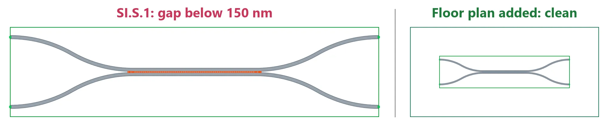
A design rule check (DRC) measures every shape of a layout against the limits of a fabrication process, such as minimum widths, minimum gaps, enclosures and the area a design may occupy. The rules are written in a rule deck that the foundry ships with its process design kit (PDK).
drc_check runs a rule deck on a PhotonForge component. It exports the component to GDSII, runs the deck in KLayout and reads the results database back into a DRCResults object, so the whole loop stays in Python. Calibre, which runs an SVRF rule deck, is also supported and returns the same results. See Layout Verification for the full API.
This guide uses SiPhoPDK, a demonstration PDK for PhotonForge: a synthetic 220 nm silicon-on-insulator process for the O-band, with silicon nitride, germanium photodiodes, a heater and two metal layers. It ships a KLayout DRC deck of 43 rules for width, space, enclosure, placement and area, and the deck states where each value comes from. SiPhoPDK is not a foundry PDK and must not be used for a tape-out.
The guide checks a directional coupler whose gap is below the minimum silicon spacing, reads the violations, draws them on the layout, and fixes the layout until the check is clean.
Prerequisites
Section titled “Prerequisites”- Install the full KLayout application, version 0.29.12 or newer, from the KLayout download page. PhotonForge searches for it in
PATHand in the common install locations; setpf.config.klayout_executablewhen it is installed elsewhere. - Install SiPhoPDK with
pip install siphopdk-forge. The rule deck is part of the package, which this guide imports aspdk.
import photonforge as pfimport siphopdk as pdkfrom photonforge.live_viewer import LiveViewer
# Start the LiveViewer to see the layouts in a browserviewer = LiveViewer()
LiveViewer started at http://127.0.0.1:35497. Call its 'stop()' method to free the port.Setting up the technology
Section titled “Setting up the technology”pdk.siphopdk() creates the SiPhoPDK technology: its layers, layer stack and port specifications. Setting it as the default makes every new component use it.
We add one annotation layer, DRC_MARKER, to draw the violations on the layout later. It is not part of the process.
# Create the SiPhoPDK technologytech = pdk.siphopdk()
# Add a layer to draw the DRC markers on, outside the layers the deck checkstech.add_layer("DRC_MARKER", pf.LayerSpec((99, 0), "DRC marker", "#ff4500cc", "xx"))
# Use the technology for every new componentpf.config.default_technology = tech
The layer specifications of SiPhoPDK also carry the basic width and spacing rules of each layer. For the silicon core layer SI, both are 150 nm:
# Minimum width and spacing stored on the silicon layer (μm)print("SI minimum width:", tech.layers["SI"].min_width)print("SI minimum spacing:", tech.layers["SI"].min_spacing)SI minimum width: 0.15SI minimum spacing: 0.15Creating a layout with violations
Section titled “Creating a layout with violations”The SiPhoPDK directional coupler, pdk.component.directional_coupler, takes coupling_distance, the distance between the centers of its two waveguides in the coupling section. The gap between the silicon edges is that distance minus the core width, 400 nm for the strip waveguide SI_STRIP_O.
We ask for a gap of 120 nm, below the 150 nm minimum spacing, so the check has something to find.
# Read the core width of the strip waveguide from its port specificationcore_width, _ = tech.ports["SI_STRIP_O"].path_profile_for("SI")
# Gap between the silicon edges in the coupling section (μm)gap = 0.12
# Build the coupler with a center-to-center distance of core width plus gapcoupler = pdk.component.directional_coupler(coupling_distance=core_width + gap)viewer(coupler)
Running DRC
Section titled “Running DRC”drc_check takes the component and the rule deck. SiPhoPDK gives the path of its deck as pdk.DRC_RULES. The deck reads the layout with source($gdsfile) and writes its report with report(..., $resultsfile); drc_check sets both variables.
The optional results_file argument keeps KLayout’s own results database, here drc_results.lyrdb. It can be opened in KLayout’s marker browser or loaded again later.
# Export the coupler, run the SiPhoPDK deck in KLayout and load the markersresults = pf.drc_check(coupler, pdk.DRC_RULES, results_file="drc_results.lyrdb")KLayout version: 0 s -
KLayout DRC: 0 s -
KLayout DRC: 1 s \
KLayout DRC: 1 s |
KLayout DRC: 1 s /
KLayout DRC: 2 s -
KLayout DRC: 2 s \
KLayout DRC: 2 s |
KLayout DRC: 2 s /
KLayout DRC: 3 s -
Reading results: 0 s -
Reading results: 1 s \
Reading results: 1 s |
Reading results: 1 s /
Reading results: 2 s -
Reading results: 2 s \
Reading results: 2 s |
Reading results: 2 s /
KLayout DRC finished in 6 sSiPhoPDK also provides pdk.drc_check(component), which is the same call with the deck filled in. The rest of this guide uses it.
Inspecting results
Section titled “Inspecting results”The output of drc_check is a DRCResults object holding the markers of every rule in the deck. results.is_clean is the verdict:
# Check whether any rule reported a violationprint("DRC clean:", results.is_clean)DRC clean: Falseprint(results) lists every rule of the deck with its count, which is long for a deck of 43 rules. results.violation_counts holds the same numbers as a dictionary, from which we keep the rules that failed:
# Keep the rules with at least one violationfailed = {rule: count for rule, count in results.violation_counts.items() if count > 0}print(failed){'FP.1': 2, 'SI.S.1': 13}Indexing the results with a rule name returns that rule’s violations, with the description written in the deck, the number of markers and the markers themselves:
# Print the description of each failed rule, as written in the deckfor rule in failed: print(f"{rule}: {results[rule].description}")FP.1: Geometry outside FLOORPLANSI.S.1: SI space < 150 nmWhat these violations mean
Section titled “What these violations mean”- SI.S.1 reports silicon shapes closer than 150 nm. The 120 nm gap of the coupling section is the main marker; the deck also marks the start of each S-bend, where the arms are still closer than the rule.
- FP.1 reports geometry outside the
FLOORPLANlayer. The SiPhoPDK deck requires every drawn shape to lie inside the floor plan of the die, and the coupler has none yet.
Where the markers are
Section titled “Where the markers are”KLayout checks the layout hierarchically, so each marker is reported once, in the cell where the violation occurs and in the coordinates of that cell. results.violated_cells lists the cells with at least one marker. results.in_top_cell(marker) moves a marker into the coordinates of the top cell. Here the coupler is the top cell, so both are the same.
# Cells with at least one violationprint(results.violated_cells)
# First 'SI.S.1' marker, a polygon in the coordinates of its cellprint(results["SI.S.1"].markers[0])('dc_lc15p0_g0p52',)PolygonMarker(cell='dc_lc15p0_g0p52', hull=((14.493, 4.191), (14.558, 4.326), (14.631, 4.325), (14.558, 4.194)), holes=())Drawing the markers on the layout
Section titled “Drawing the markers on the layout”Each SI.S.1 marker is a polygon. Adding the polygons on the DRC_MARKER layer, in a component that also holds the coupler, shows where the rule failed:
# Put the coupler and the markers together in one componentmarked = pf.Component("COUPLER_DRC")marked.add_reference(coupler)
# Draw every 'SI.S.1' marker, moved into the coordinates of the top cellfor marker in results["SI.S.1"].markers:    marker = results.in_top_cell(marker)    marked.add("DRC_MARKER", pf.Polygon(marker.hull))
viewer(marked);fill:%23221f20;font-weight:bold;font-size:0.617600px;}.terminal{fill:none;stroke:%23805080;stroke-width:0.077200;}.dashed{stroke-dasharray:0.386000,0.231600;}.port{fill:none;stroke:%23805080;stroke-width:0.154400;}.virtual-connection{fill:none;stroke:%23907090;stroke-width:0.115800;}.layer_100_0{stroke:%23009630;fill:none;}.label_100_0{fill:%23009630;}.layer_81_0{stroke:%23333333;fill:none;}.label_81_0{fill:%23333333;}.layer_99_0{stroke:%23ff4500;fill:url(%23pat-layer_99_0);fill-opacity:0.935;}.label_99_0{fill:%23ff4500;}.layer_70_0{stroke:%237591ab;fill:none;}.label_70_0{fill:%237591ab;}.layer_95_0{stroke:%23ff0000;fill:none;}.label_95_0{fill:%23ff0000;}.layer_91_0{stroke:%23b88018;fill:url(%23pat-layer_91_0);fill-opacity:0.661;}.label_91_0{fill:%23b88018;}.layer_90_0{stroke:%2378838f;fill:url(%23pat-layer_90_0);fill-opacity:0.661;}.label_90_0{fill:%2378838f;}.layer_80_0{stroke:%2300643c;fill:none;}.label_80_0{fill:%2300643c;}.layer_8_0{stroke:%2336a9cc;fill:%2338b0d4;fill-opacity:0.753;}.label_8_0{fill:%2336a9cc;}.layer_3_0{stroke:%237f6833;fill:url(%23pat-layer_3_0);fill-opacity:0.842;}.label_3_0{fill:%237f6833;}.layer_30_0{stroke:%23c0272d;fill:url(%23pat-layer_30_0);fill-opacity:0.918;}.label_30_0{fill:%23c0272d;}.layer_50_0{stroke:%23c6773e;fill:url(%23pat-layer_50_0);fill-opacity:0.895;}.label_50_0{fill:%23c6773e;}.layer_52_0{stroke:%23b88018;fill:url(%23pat-layer_52_0);fill-opacity:0.895;}.label_52_0{fill:%23b88018;}.layer_106_0{stroke:%233355ff;fill:none;}.label_106_0{fill:%233355ff;}.layer_92_0{stroke:%23878787;fill:none;}.label_92_0{fill:%23878787;}.layer_22_0{stroke:%236a975e;fill:url(%23pat-layer_22_0);fill-opacity:0.781;}.label_22_0{fill:%236a975e;}.layer_24_0{stroke:%234f9e42;fill:url(%23pat-layer_24_0);fill-opacity:0.842;}.label_24_0{fill:%234f9e42;}.layer_20_0{stroke:%235f715a;fill:url(%23pat-layer_20_0);fill-opacity:0.781;}.label_20_0{fill:%235f715a;}.layer_60_0{stroke:%237f6833;fill:%23ffd166;fill-opacity:0.690;}.label_60_0{fill:%237f6833;}.layer_101_0{stroke:%2300c853;fill:%2300c853;fill-opacity:0.502;}.label_101_0{fill:%2300c853;}.layer_102_0{stroke:%23e07b00;fill:%23ff8c00;fill-opacity:0.502;}.label_102_0{fill:%23e07b00;}.layer_23_0{stroke:%23c56d87;fill:url(%23pat-layer_23_0);fill-opacity:0.781;}.label_23_0{fill:%23c56d87;}.layer_25_0{stroke:%23c94f74;fill:url(%23pat-layer_25_0);fill-opacity:0.842;}.label_25_0{fill:%23c94f74;}.layer_21_0{stroke:%2385636d;fill:url(%23pat-layer_21_0);fill-opacity:0.781;}.label_21_0{fill:%2385636d;}.layer_1_0{stroke:%2378838f;fill:%2378838f;fill-opacity:0.753;}.label_1_0{fill:%2378838f;}.layer_5_0{stroke:%232f5fd0;fill:%232f5fd0;fill-opacity:0.753;}.label_5_0{fill:%232f5fd0;}.layer_2_0{stroke:%23838c96;fill:url(%23pat-layer_2_0);fill-opacity:0.842;}.label_2_0{fill:%23838c96;}.layer_105_0{stroke:%23202020;fill:none;}.label_105_0{fill:%23202020;}.layer_40_0{stroke:%238a5a2b;fill:%238a5a2b;fill-opacity:0.753;}.label_40_0{fill:%238a5a2b;}.layer_41_0{stroke:%238a5a2b;fill:%238a5a2b;fill-opacity:0.753;}.label_41_0{fill:%238a5a2b;}.layer_42_0{stroke:%23a3652f;fill:%23a3652f;fill-opacity:0.753;}.label_42_0{fill:%23a3652f;}</style><defs><path id=%22port-symbol%22 class=%22port%22 d=%22M 0,-0.308800 L 0.463200,0 0,0.308800%22 /><path id=%22ref-port-symbol%22 class=%22port%22 style=%22stroke-opacity:0.33;%22 d=%22M 0,-0.231600 C 0.308800,-0.231600 0.308800,0.231600 0,0.231600%22 /><circle id=%22port-bend-symbol%22 style=%22stroke-width:0;stroke:none;fill:%23805080;fill-opacity:1;%22 cx=%220%22 cy=%220%22 r=%220.138960%22 /><circle id=%22connection-symbol%22 style=%22stroke-width:0;stroke:none;fill:%23907090;fill-opacity:1;%22 cx=%220%22 cy=%220%22 r=%220.162120%22 /><pattern id=%22pat-layer_99_0%22 patternUnits=%22userSpaceOnUse%22 width=%220.231600%22 height=%220.231600%22 patternTransform=%22translate(0.177106,0.073137)%22><line x1=%220%22 y1=%220%22 x2=%220.231600%22 y2=%220.231600%22 style=%22stroke:%23ff4500;stroke-width:0.038600%22 /><line x1=%22-0.115800%22 y1=%220.115800%22 x2=%220.115800%22 y2=%220.347400%22 style=%22stroke:%23ff4500;stroke-width:0.038600%22 /><line x1=%220.115800%22 y1=%22-0.115800%22 x2=%220.347400%22 y2=%220.115800%22 style=%22stroke:%23ff4500;stroke-width:0.038600%22 /><line x1=%220.231600%22 y1=%220%22 x2=%220%22 y2=%220.231600%22 style=%22stroke:%23ff4500;stroke-width:0.038600%22 /><line x1=%220.347400%22 y1=%220.115800%22 x2=%220.115800%22 y2=%220.347400%22 style=%22stroke:%23ff4500;stroke-width:0.038600%22 /><line x1=%220.115800%22 y1=%22-0.115800%22 x2=%22-0.115800%22 y2=%220.115800%22 style=%22stroke:%23ff4500;stroke-width:0.038600%22 /></pattern><pattern id=%22pat-layer_91_0%22 patternUnits=%22userSpaceOnUse%22 width=%220.386000%22 height=%220.386000%22 patternTransform=%22translate(0.181647,0.264105)%22><circle cx=%220.193000%22 cy=%220.193000%22 r=%220.038600%22 style=%22stroke:none;fill:%23b88018;fill-opacity:1.0%22 /></pattern><pattern id=%22pat-layer_90_0%22 patternUnits=%22userSpaceOnUse%22 width=%220.386000%22 height=%220.386000%22 patternTransform=%22translate(0.022706,0.040632)%22><circle cx=%220.193000%22 cy=%220.193000%22 r=%220.038600%22 style=%22stroke:none;fill:%2378838f;fill-opacity:1.0%22 /></pattern><pattern id=%22pat-layer_3_0%22 patternUnits=%22userSpaceOnUse%22 width=%220.231600%22 height=%220.231600%22 patternTransform=%22translate(0.054494,0.170653)%22><line x1=%220.231600%22 y1=%220%22 x2=%220%22 y2=%220.231600%22 style=%22stroke:%237f6833;stroke-width:0.038600%22 /><line x1=%220.347400%22 y1=%220.115800%22 x2=%220.115800%22 y2=%220.347400%22 style=%22stroke:%237f6833;stroke-width:0.038600%22 /><line x1=%220.115800%22 y1=%22-0.115800%22 x2=%22-0.115800%22 y2=%220.115800%22 style=%22stroke:%237f6833;stroke-width:0.038600%22 /></pattern><pattern id=%22pat-layer_30_0%22 patternUnits=%22userSpaceOnUse%22 width=%220.386000%22 height=%220.386000%22 patternTransform=%22translate(0.136235,0.142211)%22><line x1=%220%22 y1=%220%22 x2=%220.386000%22 y2=%220.386000%22 style=%22stroke:%23c0272d;stroke-width:0.038600%22 /><line x1=%22-0.193000%22 y1=%220.193000%22 x2=%220.193000%22 y2=%220.579000%22 style=%22stroke:%23c0272d;stroke-width:0.038600%22 /><line x1=%220.193000%22 y1=%22-0.193000%22 x2=%220.579000%22 y2=%220.193000%22 style=%22stroke:%23c0272d;stroke-width:0.038600%22 /><line x1=%220.386000%22 y1=%220%22 x2=%220%22 y2=%220.386000%22 style=%22stroke:%23c0272d;stroke-width:0.038600%22 /><line x1=%220.579000%22 y1=%220.193000%22 x2=%220.193000%22 y2=%220.579000%22 style=%22stroke:%23c0272d;stroke-width:0.038600%22 /><line x1=%220.193000%22 y1=%22-0.193000%22 x2=%22-0.193000%22 y2=%220.193000%22 style=%22stroke:%23c0272d;stroke-width:0.038600%22 /></pattern><pattern id=%22pat-layer_50_0%22 patternUnits=%22userSpaceOnUse%22 width=%220.231600%22 height=%220.231600%22 patternTransform=%22translate(0.136235,0.219411)%22><line x1=%220.231600%22 y1=%220%22 x2=%220%22 y2=%220.231600%22 style=%22stroke:%23c6773e;stroke-width:0.038600%22 /><line x1=%220.347400%22 y1=%220.115800%22 x2=%220.115800%22 y2=%220.347400%22 style=%22stroke:%23c6773e;stroke-width:0.038600%22 /><line x1=%220.115800%22 y1=%22-0.115800%22 x2=%22-0.115800%22 y2=%220.115800%22 style=%22stroke:%23c6773e;stroke-width:0.038600%22 /></pattern><pattern id=%22pat-layer_52_0%22 patternUnits=%22userSpaceOnUse%22 width=%220.231600%22 height=%220.231600%22 patternTransform=%22translate(0.095365,0.024379)%22><line x1=%220%22 y1=%220%22 x2=%220.231600%22 y2=%220.231600%22 style=%22stroke:%23b88018;stroke-width:0.038600%22 /><line x1=%22-0.115800%22 y1=%220.115800%22 x2=%220.115800%22 y2=%220.347400%22 style=%22stroke:%23b88018;stroke-width:0.038600%22 /><line x1=%220.115800%22 y1=%22-0.115800%22 x2=%220.347400%22 y2=%220.115800%22 style=%22stroke:%23b88018;stroke-width:0.038600%22 /></pattern><pattern id=%22pat-layer_22_0%22 patternUnits=%22userSpaceOnUse%22 width=%220.231600%22 height=%220.231600%22 patternTransform=%22translate(0.013624,0.170653)%22><circle cx=%220.115800%22 cy=%220.115800%22 r=%220.038600%22 style=%22stroke:none;fill:%236a975e;fill-opacity:1.0%22 /></pattern><pattern id=%22pat-layer_24_0%22 patternUnits=%22userSpaceOnUse%22 width=%220.231600%22 height=%220.231600%22 patternTransform=%22translate(0.204353,0.207221)%22><line x1=%220%22 y1=%220%22 x2=%220.231600%22 y2=%220.231600%22 style=%22stroke:%234f9e42;stroke-width:0.038600%22 /><line x1=%22-0.115800%22 y1=%220.115800%22 x2=%220.115800%22 y2=%220.347400%22 style=%22stroke:%234f9e42;stroke-width:0.038600%22 /><line x1=%220.115800%22 y1=%22-0.115800%22 x2=%220.347400%22 y2=%220.115800%22 style=%22stroke:%234f9e42;stroke-width:0.038600%22 /><line x1=%220.231600%22 y1=%220%22 x2=%220%22 y2=%220.231600%22 style=%22stroke:%234f9e42;stroke-width:0.038600%22 /><line x1=%220.347400%22 y1=%220.115800%22 x2=%220.115800%22 y2=%220.347400%22 style=%22stroke:%234f9e42;stroke-width:0.038600%22 /><line x1=%220.115800%22 y1=%22-0.115800%22 x2=%22-0.115800%22 y2=%220.115800%22 style=%22stroke:%234f9e42;stroke-width:0.038600%22 /></pattern><pattern id=%22pat-layer_20_0%22 patternUnits=%22userSpaceOnUse%22 width=%220.386000%22 height=%220.386000%22 patternTransform=%22translate(0.090824,0.223474)%22><circle cx=%220.193000%22 cy=%220.193000%22 r=%220.038600%22 style=%22stroke:none;fill:%235f715a;fill-opacity:1.0%22 /></pattern><pattern id=%22pat-layer_23_0%22 patternUnits=%22userSpaceOnUse%22 width=%220.231600%22 height=%220.231600%22 patternTransform=%22translate(0.108988,0.073137)%22><circle cx=%220.115800%22 cy=%220.115800%22 r=%220.038600%22 style=%22stroke:none;fill:%23c56d87;fill-opacity:1.0%22 /></pattern><pattern id=%22pat-layer_25_0%22 patternUnits=%22userSpaceOnUse%22 width=%220.231600%22 height=%220.231600%22 patternTransform=%22translate(0.068118,0.109705)%22><line x1=%220%22 y1=%220%22 x2=%220.231600%22 y2=%220.231600%22 style=%22stroke:%23c94f74;stroke-width:0.038600%22 /><line x1=%22-0.115800%22 y1=%220.115800%22 x2=%220.115800%22 y2=%220.347400%22 style=%22stroke:%23c94f74;stroke-width:0.038600%22 /><line x1=%220.115800%22 y1=%22-0.115800%22 x2=%220.347400%22 y2=%220.115800%22 style=%22stroke:%23c94f74;stroke-width:0.038600%22 /><line x1=%220.231600%22 y1=%220%22 x2=%220%22 y2=%220.231600%22 style=%22stroke:%23c94f74;stroke-width:0.038600%22 /><line x1=%220.347400%22 y1=%220.115800%22 x2=%220.115800%22 y2=%220.347400%22 style=%22stroke:%23c94f74;stroke-width:0.038600%22 /><line x1=%220.115800%22 y1=%22-0.115800%22 x2=%22-0.115800%22 y2=%220.115800%22 style=%22stroke:%23c94f74;stroke-width:0.038600%22 /></pattern><pattern id=%22pat-layer_21_0%22 patternUnits=%22userSpaceOnUse%22 width=%220.386000%22 height=%220.386000%22 patternTransform=%22translate(0.249765,0.060947)%22><circle cx=%220.193000%22 cy=%220.193000%22 r=%220.038600%22 style=%22stroke:none;fill:%2385636d;fill-opacity:1.0%22 /></pattern><pattern id=%22pat-layer_2_0%22 patternUnits=%22userSpaceOnUse%22 width=%220.231600%22 height=%220.231600%22 patternTransform=%22translate(0.190729,0.036568)%22><line x1=%220%22 y1=%220%22 x2=%220.231600%22 y2=%220.231600%22 style=%22stroke:%23838c96;stroke-width:0.038600%22 /><line x1=%22-0.115800%22 y1=%220.115800%22 x2=%220.115800%22 y2=%220.347400%22 style=%22stroke:%23838c96;stroke-width:0.038600%22 /><line x1=%220.115800%22 y1=%22-0.115800%22 x2=%220.347400%22 y2=%220.115800%22 style=%22stroke:%23838c96;stroke-width:0.038600%22 /></pattern><g id=%22C1%22 data-name=%22dc_lc15p0_g0p52%22><path class=%22layer_1_0%22 d=%22M 0.000000,-0.200000 0.442000,-0.194000 0.883000,-0.174000 1.324000,-0.142000 1.764000,-0.098000 2.202000,-0.040000 2.638000,0.030000 3.072000,0.112000 3.504000,0.208000 3.933000,0.315000 4.358000,0.435000 4.780000,0.568000 5.197000,0.712000 5.610000,0.869000 6.019000,1.037000 6.423000,1.217000 6.821000,1.409000 7.213000,1.612000 7.600000,1.827000 7.976000,2.035000 8.358000,2.233000 8.746000,2.420000 9.139000,2.595000 9.537000,2.759000 9.939000,2.912000 10.346000,3.052000 10.756000,3.181000 11.170000,3.298000 11.588000,3.403000 12.008000,3.496000 12.431000,3.576000 12.856000,3.645000 13.282000,3.700000 13.711000,3.744000 14.140000,3.775000 14.570000,3.794000 15.000000,3.800000 30.000000,3.800000 30.430000,3.794000 30.860000,3.775000 31.289000,3.744000 31.718000,3.700000 32.144000,3.645000 32.569000,3.576000 32.992000,3.496000 33.412000,3.403000 33.830000,3.298000 34.244000,3.181000 34.654000,3.052000 35.061000,2.912000 35.463000,2.759000 35.861000,2.595000 36.254000,2.420000 36.642000,2.233000 37.024000,2.035000 37.400000,1.827000 37.787000,1.612000 38.179000,1.409000 38.577000,1.217000 38.981000,1.037000 39.390000,0.869000 39.803000,0.712000 40.220000,0.568000 40.642000,0.435000 41.067000,0.315000 41.496000,0.208000 41.928000,0.112000 42.362000,0.030000 42.798000,-0.040000 43.236000,-0.098000 43.676000,-0.142000 44.117000,-0.174000 44.558000,-0.194000 45.000000,-0.200000 45.000000,0.200000 44.570000,0.206000 44.140000,0.225000 43.711000,0.256000 43.282000,0.300000 42.856000,0.355000 42.431000,0.424000 42.008000,0.504000 41.588000,0.597000 41.170000,0.702000 40.756000,0.819000 40.346000,0.948000 39.939000,1.088000 39.537000,1.241000 39.139000,1.405000 38.746000,1.580000 38.358000,1.767000 37.976000,1.965000 37.600000,2.173000 37.213000,2.388000 36.821000,2.591000 36.423000,2.783000 36.019000,2.963000 35.610000,3.131000 35.197000,3.288000 34.780000,3.432000 34.358000,3.565000 33.933000,3.685000 33.504000,3.792000 33.072000,3.888000 32.638000,3.970000 32.202000,4.040000 31.764000,4.098000 31.324000,4.142000 30.883000,4.174000 30.442000,4.194000 30.000000,4.200000 15.000000,4.200000 14.558000,4.194000 14.117000,4.174000 13.676000,4.142000 13.236000,4.098000 12.798000,4.040000 12.362000,3.970000 11.928000,3.888000 11.496000,3.792000 11.067000,3.685000 10.642000,3.565000 10.220000,3.432000 9.803000,3.288000 9.390000,3.131000 8.981000,2.963000 8.577000,2.783000 8.179000,2.591000 7.787000,2.388000 7.400000,2.173000 7.024000,1.965000 6.642000,1.767000 6.254000,1.580000 5.861000,1.405000 5.463000,1.241000 5.061000,1.088000 4.654000,0.948000 4.244000,0.819000 3.830000,0.702000 3.412000,0.597000 2.992000,0.504000 2.569000,0.424000 2.144000,0.355000 1.718000,0.300000 1.289000,0.256000 0.860000,0.225000 0.430000,0.206000 0.000000,0.200000 z%22 /><path class=%22layer_1_0%22 d=%22M 45.000000,8.720000 44.558000,8.714000 44.117000,8.694000 43.676000,8.662000 43.236000,8.618000 42.798000,8.560000 42.362000,8.490000 41.928000,8.408000 41.496000,8.312000 41.067000,8.205000 40.642000,8.085000 40.220000,7.952000 39.803000,7.808000 39.390000,7.651000 38.981000,7.483000 38.577000,7.303000 38.179000,7.111000 37.787000,6.908000 37.400000,6.693000 37.024000,6.485000 36.642000,6.287000 36.254000,6.100000 35.861000,5.925000 35.463000,5.761000 35.061000,5.608000 34.654000,5.468000 34.244000,5.339000 33.830000,5.222000 33.412000,5.117000 32.992000,5.024000 32.569000,4.944000 32.144000,4.875000 31.718000,4.820000 31.289000,4.776000 30.860000,4.745000 30.430000,4.726000 30.000000,4.720000 15.000000,4.720000 14.570000,4.726000 14.140000,4.745000 13.711000,4.776000 13.282000,4.820000 12.856000,4.875000 12.431000,4.944000 12.008000,5.024000 11.588000,5.117000 11.170000,5.222000 10.756000,5.339000 10.346000,5.468000 9.939000,5.608000 9.537000,5.761000 9.139000,5.925000 8.746000,6.100000 8.358000,6.287000 7.976000,6.485000 7.600000,6.693000 7.213000,6.908000 6.821000,7.111000 6.423000,7.303000 6.019000,7.483000 5.610000,7.651000 5.197000,7.808000 4.780000,7.952000 4.358000,8.085000 3.933000,8.205000 3.504000,8.312000 3.072000,8.408000 2.638000,8.490000 2.202000,8.560000 1.764000,8.618000 1.324000,8.662000 0.883000,8.694000 0.442000,8.714000 0.000000,8.720000 0.000000,8.320000 0.430000,8.314000 0.860000,8.295000 1.289000,8.264000 1.718000,8.220000 2.144000,8.165000 2.569000,8.096000 2.992000,8.016000 3.412000,7.923000 3.830000,7.818000 4.244000,7.701000 4.654000,7.572000 5.061000,7.432000 5.463000,7.279000 5.861000,7.115000 6.254000,6.940000 6.642000,6.753000 7.024000,6.555000 7.400000,6.347000 7.787000,6.132000 8.179000,5.929000 8.577000,5.737000 8.981000,5.557000 9.390000,5.389000 9.803000,5.232000 10.220000,5.088000 10.642000,4.955000 11.067000,4.835000 11.496000,4.728000 11.928000,4.632000 12.362000,4.550000 12.798000,4.480000 13.236000,4.422000 13.676000,4.378000 14.117000,4.346000 14.558000,4.326000 15.000000,4.320000 30.000000,4.320000 30.442000,4.326000 30.883000,4.346000 31.324000,4.378000 31.764000,4.422000 32.202000,4.480000 32.638000,4.550000 33.072000,4.632000 33.504000,4.728000 33.933000,4.835000 34.358000,4.955000 34.780000,5.088000 35.197000,5.232000 35.610000,5.389000 36.019000,5.557000 36.423000,5.737000 36.821000,5.929000 37.213000,6.132000 37.600000,6.347000 37.976000,6.555000 38.358000,6.753000 38.746000,6.940000 39.139000,7.115000 39.537000,7.279000 39.939000,7.432000 40.346000,7.572000 40.756000,7.701000 41.170000,7.818000 41.588000,7.923000 42.008000,8.016000 42.431000,8.096000 42.856000,8.165000 43.282000,8.220000 43.711000,8.264000 44.140000,8.295000 44.570000,8.314000 45.000000,8.320000 z%22 /><rect class=%22layer_100_0%22 x=%220.000000%22 y=%22-1.200000%22 width=%2245.000000%22 height=%2210.920000%22 /><rect class=%22layer_101_0%22 x=%22-0.100000%22 y=%22-0.100000%22 width=%220.200000%22 height=%220.200000%22 /><rect class=%22layer_101_0%22 x=%22-0.100000%22 y=%228.420000%22 width=%220.200000%22 height=%220.200000%22 /><rect class=%22layer_101_0%22 x=%2244.900000%22 y=%22-0.100000%22 width=%220.200000%22 height=%220.200000%22 /><rect class=%22layer_101_0%22 x=%2244.900000%22 y=%228.420000%22 width=%220.200000%22 height=%220.200000%22 /></g></defs><g transform=%22scale(1 -1)%22><g id=%22C0%22 data-name=%22COUPLER_DRC%22><use transform=%22translate(0.000000 0.000000)%22 href=%22%23C1%22 /><path class=%22layer_99_0%22 d=%22M 14.558000,4.194000 14.631000,4.325000 14.558000,4.326000 14.493000,4.191000 z%22 /><path class=%22layer_99_0%22 d=%22M 15.000000,4.200000 15.000000,4.320000 14.558000,4.326000 14.558000,4.194000 z%22 /><path class=%22layer_99_0%22 d=%22M 14.558000,4.194000 14.558000,4.326000 14.358000,4.335000 14.358000,4.185000 z%22 /><path class=%22layer_99_0%22 d=%22M 15.090000,4.200000 15.000000,4.320000 14.912000,4.321000 15.000000,4.200000 z%22 /><path class=%22layer_99_0%22 d=%22M 15.000000,4.200000 15.090000,4.320000 15.000000,4.320000 14.912000,4.199000 z%22 /><path class=%22layer_99_0%22 d=%22M 30.642000,4.335000 30.442000,4.326000 30.442000,4.194000 30.642000,4.185000 z%22 /><path class=%22layer_99_0%22 d=%22M 30.000000,4.200000 30.000000,4.320000 15.000000,4.320000 15.000000,4.200000 z%22 /><path class=%22layer_99_0%22 d=%22M 30.000000,4.320000 29.910000,4.320000 30.000000,4.200000 30.088000,4.199000 z%22 /><path class=%22layer_99_0%22 d=%22M 30.000000,4.200000 30.088000,4.321000 30.000000,4.320000 29.910000,4.200000 z%22 /><path class=%22layer_99_0%22 d=%22M 30.442000,4.326000 30.000000,4.320000 30.000000,4.200000 30.442000,4.194000 z%22 /><path class=%22layer_99_0%22 d=%22M 14.631000,4.195000 14.558000,4.326000 14.493000,4.329000 14.558000,4.194000 z%22 /><path class=%22layer_99_0%22 d=%22M 30.507000,4.329000 30.442000,4.326000 30.369000,4.195000 30.442000,4.194000 z%22 /><path class=%22layer_99_0%22 d=%22M 30.442000,4.326000 30.369000,4.325000 30.442000,4.194000 30.507000,4.191000 z%22 /></g></g></svg>)
%22><use href=%22%23g-dc%22 transform=%22translate(-30.00 -30.00) scale(1.2)%22/><circle cx=%22-30.00%22 cy=%22-6.54%22 r=%224%22 fill=%22%2300643c%22 stroke=%22%2300643c%22 stroke-width=%221%22/><circle cx=%22-30.00%22 cy=%2210.05%22 r=%224%22 fill=%22%2300643c%22 stroke=%22%2300643c%22 stroke-width=%221%22/><circle cx=%2230.00%22 cy=%22-6.51%22 r=%224%22 fill=%22%2300643c%22 stroke=%22%2300643c%22 stroke-width=%221%22/><circle cx=%2230.00%22 cy=%2210.17%22 r=%224%22 fill=%22%2300643c%22 stroke=%22%2300643c%22 stroke-width=%221%22/></g><text x=%220.00%22 y=%2231.80%22 font-size=%229%22 fill=%22%23232530%22 font-weight=%22400%22 text-anchor=%22middle%22 dominant-baseline=%22hanging%22 stroke=%22%23ffffff%22 stroke-width=%223.15%22 stroke-linejoin=%22round%22 paint-order=%22stroke%22>dc_lc15p0_g0p52_1</text><g fill=%22none%22 stroke-width=%222%22></g></svg>)
A results database written earlier can be read back with load_drc_results, without running the check again:
# Read the saved results databasesaved = pf.load_drc_results("drc_results.lyrdb", show_progress=False)print({rule: count for rule, count in saved.violation_counts.items() if count > 0}){'FP.1': 2, 'SI.S.1': 13}Fixing the violations
Section titled “Fixing the violations”We fix the two rules in turn:
- SI.S.1: widen the gap to 200 nm. The coupler is a parametric component, so
updaterebuilds it with the new distance. - FP.1: place the coupler on a die that has a floor plan around it.
# Widen the gap to 200 nm, which rebuilds the couplercoupler.update(coupling_distance=core_width + 0.2)
# Check the coupler again with the SiPhoPDK deckresults = pdk.drc_check(coupler, show_progress=False)print({rule: count for rule, count in results.violation_counts.items() if count > 0})
{'FP.1': 2}Only FP.1 is left. A die is a cell that holds the design and the FLOORPLAN rectangle that encloses it. envelope gives a box around the coupler, enlarged by a margin:
# Margin between the coupler and the edge of the floor plan (μm)margin = 10.0
# Place the coupler on a die with a floor plan around itdie = pf.Component("COUPLER_DIE")die.add_reference(coupler)die.add("FLOORPLAN", pf.envelope(coupler, offset=margin, use_box=True))viewer(die);fill:%23221f20;font-weight:bold;font-size:1.500800px;}.terminal{fill:none;stroke:%23805080;stroke-width:0.187600;}.dashed{stroke-dasharray:0.938000,0.562800;}.port{fill:none;stroke:%23805080;stroke-width:0.375200;}.virtual-connection{fill:none;stroke:%23907090;stroke-width:0.281400;}.layer_100_0{stroke:%23009630;fill:none;}.label_100_0{fill:%23009630;}.layer_81_0{stroke:%23333333;fill:none;}.label_81_0{fill:%23333333;}.layer_99_0{stroke:%23ff4500;fill:url(%23pat-layer_99_0);fill-opacity:0.935;}.label_99_0{fill:%23ff4500;}.layer_70_0{stroke:%237591ab;fill:none;}.label_70_0{fill:%237591ab;}.layer_95_0{stroke:%23ff0000;fill:none;}.label_95_0{fill:%23ff0000;}.layer_91_0{stroke:%23b88018;fill:url(%23pat-layer_91_0);fill-opacity:0.661;}.label_91_0{fill:%23b88018;}.layer_90_0{stroke:%2378838f;fill:url(%23pat-layer_90_0);fill-opacity:0.661;}.label_90_0{fill:%2378838f;}.layer_80_0{stroke:%2300643c;fill:none;}.label_80_0{fill:%2300643c;}.layer_8_0{stroke:%2336a9cc;fill:%2338b0d4;fill-opacity:0.753;}.label_8_0{fill:%2336a9cc;}.layer_3_0{stroke:%237f6833;fill:url(%23pat-layer_3_0);fill-opacity:0.842;}.label_3_0{fill:%237f6833;}.layer_30_0{stroke:%23c0272d;fill:url(%23pat-layer_30_0);fill-opacity:0.918;}.label_30_0{fill:%23c0272d;}.layer_50_0{stroke:%23c6773e;fill:url(%23pat-layer_50_0);fill-opacity:0.895;}.label_50_0{fill:%23c6773e;}.layer_52_0{stroke:%23b88018;fill:url(%23pat-layer_52_0);fill-opacity:0.895;}.label_52_0{fill:%23b88018;}.layer_106_0{stroke:%233355ff;fill:none;}.label_106_0{fill:%233355ff;}.layer_92_0{stroke:%23878787;fill:none;}.label_92_0{fill:%23878787;}.layer_22_0{stroke:%236a975e;fill:url(%23pat-layer_22_0);fill-opacity:0.781;}.label_22_0{fill:%236a975e;}.layer_24_0{stroke:%234f9e42;fill:url(%23pat-layer_24_0);fill-opacity:0.842;}.label_24_0{fill:%234f9e42;}.layer_20_0{stroke:%235f715a;fill:url(%23pat-layer_20_0);fill-opacity:0.781;}.label_20_0{fill:%235f715a;}.layer_60_0{stroke:%237f6833;fill:%23ffd166;fill-opacity:0.690;}.label_60_0{fill:%237f6833;}.layer_101_0{stroke:%2300c853;fill:%2300c853;fill-opacity:0.502;}.label_101_0{fill:%2300c853;}.layer_102_0{stroke:%23e07b00;fill:%23ff8c00;fill-opacity:0.502;}.label_102_0{fill:%23e07b00;}.layer_23_0{stroke:%23c56d87;fill:url(%23pat-layer_23_0);fill-opacity:0.781;}.label_23_0{fill:%23c56d87;}.layer_25_0{stroke:%23c94f74;fill:url(%23pat-layer_25_0);fill-opacity:0.842;}.label_25_0{fill:%23c94f74;}.layer_21_0{stroke:%2385636d;fill:url(%23pat-layer_21_0);fill-opacity:0.781;}.label_21_0{fill:%2385636d;}.layer_1_0{stroke:%2378838f;fill:%2378838f;fill-opacity:0.753;}.label_1_0{fill:%2378838f;}.layer_5_0{stroke:%232f5fd0;fill:%232f5fd0;fill-opacity:0.753;}.label_5_0{fill:%232f5fd0;}.layer_2_0{stroke:%23838c96;fill:url(%23pat-layer_2_0);fill-opacity:0.842;}.label_2_0{fill:%23838c96;}.layer_105_0{stroke:%23202020;fill:none;}.label_105_0{fill:%23202020;}.layer_40_0{stroke:%238a5a2b;fill:%238a5a2b;fill-opacity:0.753;}.label_40_0{fill:%238a5a2b;}.layer_41_0{stroke:%238a5a2b;fill:%238a5a2b;fill-opacity:0.753;}.label_41_0{fill:%238a5a2b;}.layer_42_0{stroke:%23a3652f;fill:%23a3652f;fill-opacity:0.753;}.label_42_0{fill:%23a3652f;}</style><defs><path id=%22port-symbol%22 class=%22port%22 d=%22M 0,-0.750400 L 1.125600,0 0,0.750400%22 /><path id=%22ref-port-symbol%22 class=%22port%22 style=%22stroke-opacity:0.33;%22 d=%22M 0,-0.562800 C 0.750400,-0.562800 0.750400,0.562800 0,0.562800%22 /><circle id=%22port-bend-symbol%22 style=%22stroke-width:0;stroke:none;fill:%23805080;fill-opacity:1;%22 cx=%220%22 cy=%220%22 r=%220.337680%22 /><circle id=%22connection-symbol%22 style=%22stroke-width:0;stroke:none;fill:%23907090;fill-opacity:1;%22 cx=%220%22 cy=%220%22 r=%220.393960%22 /><pattern id=%22pat-layer_99_0%22 patternUnits=%22userSpaceOnUse%22 width=%220.562800%22 height=%220.562800%22 patternTransform=%22translate(0.430376,0.177726)%22><line x1=%220%22 y1=%220%22 x2=%220.562800%22 y2=%220.562800%22 style=%22stroke:%23ff4500;stroke-width:0.093800%22 /><line x1=%22-0.281400%22 y1=%220.281400%22 x2=%220.281400%22 y2=%220.844200%22 style=%22stroke:%23ff4500;stroke-width:0.093800%22 /><line x1=%220.281400%22 y1=%22-0.281400%22 x2=%220.844200%22 y2=%220.281400%22 style=%22stroke:%23ff4500;stroke-width:0.093800%22 /><line x1=%220.562800%22 y1=%220%22 x2=%220%22 y2=%220.562800%22 style=%22stroke:%23ff4500;stroke-width:0.093800%22 /><line x1=%220.844200%22 y1=%220.281400%22 x2=%220.281400%22 y2=%220.844200%22 style=%22stroke:%23ff4500;stroke-width:0.093800%22 /><line x1=%220.281400%22 y1=%22-0.281400%22 x2=%22-0.281400%22 y2=%220.281400%22 style=%22stroke:%23ff4500;stroke-width:0.093800%22 /></pattern><pattern id=%22pat-layer_91_0%22 patternUnits=%22userSpaceOnUse%22 width=%220.938000%22 height=%220.938000%22 patternTransform=%22translate(0.441412,0.641789)%22><circle cx=%220.469000%22 cy=%220.469000%22 r=%220.093800%22 style=%22stroke:none;fill:%23b88018;fill-opacity:1.0%22 /></pattern><pattern id=%22pat-layer_90_0%22 patternUnits=%22userSpaceOnUse%22 width=%220.938000%22 height=%220.938000%22 patternTransform=%22translate(0.055176,0.098737)%22><circle cx=%220.469000%22 cy=%220.469000%22 r=%220.093800%22 style=%22stroke:none;fill:%2378838f;fill-opacity:1.0%22 /></pattern><pattern id=%22pat-layer_3_0%22 patternUnits=%22userSpaceOnUse%22 width=%220.562800%22 height=%220.562800%22 patternTransform=%22translate(0.132424,0.414695)%22><line x1=%220.562800%22 y1=%220%22 x2=%220%22 y2=%220.562800%22 style=%22stroke:%237f6833;stroke-width:0.093800%22 /><line x1=%220.844200%22 y1=%220.281400%22 x2=%220.281400%22 y2=%220.844200%22 style=%22stroke:%237f6833;stroke-width:0.093800%22 /><line x1=%220.281400%22 y1=%22-0.281400%22 x2=%22-0.281400%22 y2=%220.281400%22 style=%22stroke:%237f6833;stroke-width:0.093800%22 /></pattern><pattern id=%22pat-layer_30_0%22 patternUnits=%22userSpaceOnUse%22 width=%220.938000%22 height=%220.938000%22 patternTransform=%22translate(0.331059,0.345579)%22><line x1=%220%22 y1=%220%22 x2=%220.938000%22 y2=%220.938000%22 style=%22stroke:%23c0272d;stroke-width:0.093800%22 /><line x1=%22-0.469000%22 y1=%220.469000%22 x2=%220.469000%22 y2=%221.407000%22 style=%22stroke:%23c0272d;stroke-width:0.093800%22 /><line x1=%220.469000%22 y1=%22-0.469000%22 x2=%221.407000%22 y2=%220.469000%22 style=%22stroke:%23c0272d;stroke-width:0.093800%22 /><line x1=%220.938000%22 y1=%220%22 x2=%220%22 y2=%220.938000%22 style=%22stroke:%23c0272d;stroke-width:0.093800%22 /><line x1=%221.407000%22 y1=%220.469000%22 x2=%220.469000%22 y2=%221.407000%22 style=%22stroke:%23c0272d;stroke-width:0.093800%22 /><line x1=%220.469000%22 y1=%22-0.469000%22 x2=%22-0.469000%22 y2=%220.469000%22 style=%22stroke:%23c0272d;stroke-width:0.093800%22 /></pattern><pattern id=%22pat-layer_50_0%22 patternUnits=%22userSpaceOnUse%22 width=%220.562800%22 height=%220.562800%22 patternTransform=%22translate(0.331059,0.533179)%22><line x1=%220.562800%22 y1=%220%22 x2=%220%22 y2=%220.562800%22 style=%22stroke:%23c6773e;stroke-width:0.093800%22 /><line x1=%220.844200%22 y1=%220.281400%22 x2=%220.281400%22 y2=%220.844200%22 style=%22stroke:%23c6773e;stroke-width:0.093800%22 /><line x1=%220.281400%22 y1=%22-0.281400%22 x2=%22-0.281400%22 y2=%220.281400%22 style=%22stroke:%23c6773e;stroke-width:0.093800%22 /></pattern><pattern id=%22pat-layer_52_0%22 patternUnits=%22userSpaceOnUse%22 width=%220.562800%22 height=%220.562800%22 patternTransform=%22translate(0.231741,0.059242)%22><line x1=%220%22 y1=%220%22 x2=%220.562800%22 y2=%220.562800%22 style=%22stroke:%23b88018;stroke-width:0.093800%22 /><line x1=%22-0.281400%22 y1=%220.281400%22 x2=%220.281400%22 y2=%220.844200%22 style=%22stroke:%23b88018;stroke-width:0.093800%22 /><line x1=%220.281400%22 y1=%22-0.281400%22 x2=%220.844200%22 y2=%220.281400%22 style=%22stroke:%23b88018;stroke-width:0.093800%22 /></pattern><pattern id=%22pat-layer_22_0%22 patternUnits=%22userSpaceOnUse%22 width=%220.562800%22 height=%220.562800%22 patternTransform=%22translate(0.033106,0.414695)%22><circle cx=%220.281400%22 cy=%220.281400%22 r=%220.093800%22 style=%22stroke:none;fill:%236a975e;fill-opacity:1.0%22 /></pattern><pattern id=%22pat-layer_24_0%22 patternUnits=%22userSpaceOnUse%22 width=%220.562800%22 height=%220.562800%22 patternTransform=%22translate(0.496588,0.503558)%22><line x1=%220%22 y1=%220%22 x2=%220.562800%22 y2=%220.562800%22 style=%22stroke:%234f9e42;stroke-width:0.093800%22 /><line x1=%22-0.281400%22 y1=%220.281400%22 x2=%220.281400%22 y2=%220.844200%22 style=%22stroke:%234f9e42;stroke-width:0.093800%22 /><line x1=%220.281400%22 y1=%22-0.281400%22 x2=%220.844200%22 y2=%220.281400%22 style=%22stroke:%234f9e42;stroke-width:0.093800%22 /><line x1=%220.562800%22 y1=%220%22 x2=%220%22 y2=%220.562800%22 style=%22stroke:%234f9e42;stroke-width:0.093800%22 /><line x1=%220.844200%22 y1=%220.281400%22 x2=%220.281400%22 y2=%220.844200%22 style=%22stroke:%234f9e42;stroke-width:0.093800%22 /><line x1=%220.281400%22 y1=%22-0.281400%22 x2=%22-0.281400%22 y2=%220.281400%22 style=%22stroke:%234f9e42;stroke-width:0.093800%22 /></pattern><pattern id=%22pat-layer_20_0%22 patternUnits=%22userSpaceOnUse%22 width=%220.938000%22 height=%220.938000%22 patternTransform=%22translate(0.220706,0.543053)%22><circle cx=%220.469000%22 cy=%220.469000%22 r=%220.093800%22 style=%22stroke:none;fill:%235f715a;fill-opacity:1.0%22 /></pattern><pattern id=%22pat-layer_23_0%22 patternUnits=%22userSpaceOnUse%22 width=%220.562800%22 height=%220.562800%22 patternTransform=%22translate(0.264847,0.177726)%22><circle cx=%220.281400%22 cy=%220.281400%22 r=%220.093800%22 style=%22stroke:none;fill:%23c56d87;fill-opacity:1.0%22 /></pattern><pattern id=%22pat-layer_25_0%22 patternUnits=%22userSpaceOnUse%22 width=%220.562800%22 height=%220.562800%22 patternTransform=%22translate(0.165529,0.266589)%22><line x1=%220%22 y1=%220%22 x2=%220.562800%22 y2=%220.562800%22 style=%22stroke:%23c94f74;stroke-width:0.093800%22 /><line x1=%22-0.281400%22 y1=%220.281400%22 x2=%220.281400%22 y2=%220.844200%22 style=%22stroke:%23c94f74;stroke-width:0.093800%22 /><line x1=%220.281400%22 y1=%22-0.281400%22 x2=%220.844200%22 y2=%220.281400%22 style=%22stroke:%23c94f74;stroke-width:0.093800%22 /><line x1=%220.562800%22 y1=%220%22 x2=%220%22 y2=%220.562800%22 style=%22stroke:%23c94f74;stroke-width:0.093800%22 /><line x1=%220.844200%22 y1=%220.281400%22 x2=%220.281400%22 y2=%220.844200%22 style=%22stroke:%23c94f74;stroke-width:0.093800%22 /><line x1=%220.281400%22 y1=%22-0.281400%22 x2=%22-0.281400%22 y2=%220.281400%22 style=%22stroke:%23c94f74;stroke-width:0.093800%22 /></pattern><pattern id=%22pat-layer_21_0%22 patternUnits=%22userSpaceOnUse%22 width=%220.938000%22 height=%220.938000%22 patternTransform=%22translate(0.606941,0.148105)%22><circle cx=%220.469000%22 cy=%220.469000%22 r=%220.093800%22 style=%22stroke:none;fill:%2385636d;fill-opacity:1.0%22 /></pattern><pattern id=%22pat-layer_2_0%22 patternUnits=%22userSpaceOnUse%22 width=%220.562800%22 height=%220.562800%22 patternTransform=%22translate(0.463482,0.088863)%22><line x1=%220%22 y1=%220%22 x2=%220.562800%22 y2=%220.562800%22 style=%22stroke:%23838c96;stroke-width:0.093800%22 /><line x1=%22-0.281400%22 y1=%220.281400%22 x2=%220.281400%22 y2=%220.844200%22 style=%22stroke:%23838c96;stroke-width:0.093800%22 /><line x1=%220.281400%22 y1=%22-0.281400%22 x2=%220.844200%22 y2=%220.281400%22 style=%22stroke:%23838c96;stroke-width:0.093800%22 /></pattern><g id=%22C1%22 data-name=%22dc_lc15p0_g0p6000000000000001%22><path class=%22layer_1_0%22 d=%22M 0.000000,-0.200000 0.442000,-0.194000 0.883000,-0.174000 1.324000,-0.142000 1.764000,-0.098000 2.202000,-0.040000 2.638000,0.030000 3.072000,0.112000 3.504000,0.208000 3.933000,0.315000 4.358000,0.435000 4.780000,0.568000 5.197000,0.712000 5.610000,0.869000 6.019000,1.037000 6.423000,1.217000 6.821000,1.409000 7.213000,1.612000 7.600000,1.827000 7.976000,2.035000 8.358000,2.233000 8.746000,2.420000 9.139000,2.595000 9.537000,2.759000 9.939000,2.912000 10.346000,3.052000 10.756000,3.181000 11.170000,3.298000 11.588000,3.403000 12.008000,3.496000 12.431000,3.576000 12.856000,3.645000 13.282000,3.700000 13.711000,3.744000 14.140000,3.775000 14.570000,3.794000 15.000000,3.800000 30.000000,3.800000 30.430000,3.794000 30.860000,3.775000 31.289000,3.744000 31.718000,3.700000 32.144000,3.645000 32.569000,3.576000 32.992000,3.496000 33.412000,3.403000 33.830000,3.298000 34.244000,3.181000 34.654000,3.052000 35.061000,2.912000 35.463000,2.759000 35.861000,2.595000 36.254000,2.420000 36.642000,2.233000 37.024000,2.035000 37.400000,1.827000 37.787000,1.612000 38.179000,1.409000 38.577000,1.217000 38.981000,1.037000 39.390000,0.869000 39.803000,0.712000 40.220000,0.568000 40.642000,0.435000 41.067000,0.315000 41.496000,0.208000 41.928000,0.112000 42.362000,0.030000 42.798000,-0.040000 43.236000,-0.098000 43.676000,-0.142000 44.117000,-0.174000 44.558000,-0.194000 45.000000,-0.200000 45.000000,0.200000 44.570000,0.206000 44.140000,0.225000 43.711000,0.256000 43.282000,0.300000 42.856000,0.355000 42.431000,0.424000 42.008000,0.504000 41.588000,0.597000 41.170000,0.702000 40.756000,0.819000 40.346000,0.948000 39.939000,1.088000 39.537000,1.241000 39.139000,1.405000 38.746000,1.580000 38.358000,1.767000 37.976000,1.965000 37.600000,2.173000 37.213000,2.388000 36.821000,2.591000 36.423000,2.783000 36.019000,2.963000 35.610000,3.131000 35.197000,3.288000 34.780000,3.432000 34.358000,3.565000 33.933000,3.685000 33.504000,3.792000 33.072000,3.888000 32.638000,3.970000 32.202000,4.040000 31.764000,4.098000 31.324000,4.142000 30.883000,4.174000 30.442000,4.194000 30.000000,4.200000 15.000000,4.200000 14.558000,4.194000 14.117000,4.174000 13.676000,4.142000 13.236000,4.098000 12.798000,4.040000 12.362000,3.970000 11.928000,3.888000 11.496000,3.792000 11.067000,3.685000 10.642000,3.565000 10.220000,3.432000 9.803000,3.288000 9.390000,3.131000 8.981000,2.963000 8.577000,2.783000 8.179000,2.591000 7.787000,2.388000 7.400000,2.173000 7.024000,1.965000 6.642000,1.767000 6.254000,1.580000 5.861000,1.405000 5.463000,1.241000 5.061000,1.088000 4.654000,0.948000 4.244000,0.819000 3.830000,0.702000 3.412000,0.597000 2.992000,0.504000 2.569000,0.424000 2.144000,0.355000 1.718000,0.300000 1.289000,0.256000 0.860000,0.225000 0.430000,0.206000 0.000000,0.200000 z%22 /><path class=%22layer_1_0%22 d=%22M 45.000000,8.800000 44.558000,8.794000 44.117000,8.774000 43.676000,8.742000 43.236000,8.698000 42.798000,8.640000 42.362000,8.570000 41.928000,8.488000 41.496000,8.392000 41.067000,8.285000 40.642000,8.165000 40.220000,8.032000 39.803000,7.888000 39.390000,7.731000 38.981000,7.563000 38.577000,7.383000 38.179000,7.191000 37.787000,6.988000 37.400000,6.773000 37.024000,6.565000 36.642000,6.367000 36.254000,6.180000 35.861000,6.005000 35.463000,5.841000 35.061000,5.688000 34.654000,5.548000 34.244000,5.419000 33.830000,5.302000 33.412000,5.197000 32.992000,5.104000 32.569000,5.024000 32.144000,4.955000 31.718000,4.900000 31.289000,4.856000 30.860000,4.825000 30.430000,4.806000 30.000000,4.800000 15.000000,4.800000 14.570000,4.806000 14.140000,4.825000 13.711000,4.856000 13.282000,4.900000 12.856000,4.955000 12.431000,5.024000 12.008000,5.104000 11.588000,5.197000 11.170000,5.302000 10.756000,5.419000 10.346000,5.548000 9.939000,5.688000 9.537000,5.841000 9.139000,6.005000 8.746000,6.180000 8.358000,6.367000 7.976000,6.565000 7.600000,6.773000 7.213000,6.988000 6.821000,7.191000 6.423000,7.383000 6.019000,7.563000 5.610000,7.731000 5.197000,7.888000 4.780000,8.032000 4.358000,8.165000 3.933000,8.285000 3.504000,8.392000 3.072000,8.488000 2.638000,8.570000 2.202000,8.640000 1.764000,8.698000 1.324000,8.742000 0.883000,8.774000 0.442000,8.794000 0.000000,8.800000 0.000000,8.400000 0.430000,8.394000 0.860000,8.375000 1.289000,8.344000 1.718000,8.300000 2.144000,8.245000 2.569000,8.176000 2.992000,8.096000 3.412000,8.003000 3.830000,7.898000 4.244000,7.781000 4.654000,7.652000 5.061000,7.512000 5.463000,7.359000 5.861000,7.195000 6.254000,7.020000 6.642000,6.833000 7.024000,6.635000 7.400000,6.427000 7.787000,6.212000 8.179000,6.009000 8.577000,5.817000 8.981000,5.637000 9.390000,5.469000 9.803000,5.312000 10.220000,5.168000 10.642000,5.035000 11.067000,4.915000 11.496000,4.808000 11.928000,4.712000 12.362000,4.630000 12.798000,4.560000 13.236000,4.502000 13.676000,4.458000 14.117000,4.426000 14.558000,4.406000 15.000000,4.400000 30.000000,4.400000 30.442000,4.406000 30.883000,4.426000 31.324000,4.458000 31.764000,4.502000 32.202000,4.560000 32.638000,4.630000 33.072000,4.712000 33.504000,4.808000 33.933000,4.915000 34.358000,5.035000 34.780000,5.168000 35.197000,5.312000 35.610000,5.469000 36.019000,5.637000 36.423000,5.817000 36.821000,6.009000 37.213000,6.212000 37.600000,6.427000 37.976000,6.635000 38.358000,6.833000 38.746000,7.020000 39.139000,7.195000 39.537000,7.359000 39.939000,7.512000 40.346000,7.652000 40.756000,7.781000 41.170000,7.898000 41.588000,8.003000 42.008000,8.096000 42.431000,8.176000 42.856000,8.245000 43.282000,8.300000 43.711000,8.344000 44.140000,8.375000 44.570000,8.394000 45.000000,8.400000 z%22 /><rect class=%22layer_100_0%22 x=%220.000000%22 y=%22-1.200000%22 width=%2245.000000%22 height=%2211.000000%22 /><rect class=%22layer_101_0%22 x=%22-0.100000%22 y=%22-0.100000%22 width=%220.200000%22 height=%220.200000%22 /><rect class=%22layer_101_0%22 x=%22-0.100000%22 y=%228.500000%22 width=%220.200000%22 height=%220.200000%22 /><rect class=%22layer_101_0%22 x=%2244.900000%22 y=%22-0.100000%22 width=%220.200000%22 height=%220.200000%22 /><rect class=%22layer_101_0%22 x=%2244.900000%22 y=%228.500000%22 width=%220.200000%22 height=%220.200000%22 /></g></defs><g transform=%22scale(1 -1)%22><g id=%22C0%22 data-name=%22COUPLER_DIE%22><use transform=%22translate(0.000000 0.000000)%22 href=%22%23C1%22 /><rect class=%22layer_80_0%22 x=%22-10.100000%22 y=%22-11.200000%22 width=%2265.200000%22 height=%2231.000000%22 /></g></g></svg>)
%22><use href=%22%23g-dc%22 transform=%22translate(-30.00 -30.00) scale(1.2)%22/><circle cx=%22-30.00%22 cy=%22-6.54%22 r=%224%22 fill=%22%2300643c%22 stroke=%22%2300643c%22 stroke-width=%221%22/><circle cx=%22-30.00%22 cy=%2210.05%22 r=%224%22 fill=%22%2300643c%22 stroke=%22%2300643c%22 stroke-width=%221%22/><circle cx=%2230.00%22 cy=%22-6.51%22 r=%224%22 fill=%22%2300643c%22 stroke=%22%2300643c%22 stroke-width=%221%22/><circle cx=%2230.00%22 cy=%2210.17%22 r=%224%22 fill=%22%2300643c%22 stroke=%22%2300643c%22 stroke-width=%221%22/></g><text x=%220.00%22 y=%2231.80%22 font-size=%229%22 fill=%22%23232530%22 font-weight=%22400%22 text-anchor=%22middle%22 dominant-baseline=%22hanging%22 stroke=%22%23ffffff%22 stroke-width=%223.15%22 stroke-linejoin=%22round%22 paint-order=%22stroke%22>dc_lc15p0_g0p6000000000000001_1</text><g fill=%22none%22 stroke-width=%222%22></g></svg>)
# Check the die with the SiPhoPDK deckresults = pdk.drc_check(die, show_progress=False)print("DRC clean:", results.is_clean)DRC clean: TrueThe die passes every rule of the deck.
Other ways to run DRC
Section titled “Other ways to run DRC”- Another rule deck.
pf.drc_check(component, "deck.drc")runs any KLayout deck that reads$gdsfileand writes$resultsfile. A deck that uses other variable names is driven withvariable_names, for examplevariable_names={"gdsfile": "input", "resultsfile": "report"}. Withengine="calibre", the deck is an SVRF rule deck run by Calibre. - Waivers. Geometry inside the SiPhoPDK layer
EXCL_DRC(95, 0) is waived by the deck. Other PDKs have their own waiver layers. - The LiveViewer. The LiveViewer has a DRC section that runs a rule deck on the component on screen, with KLayout or Calibre, and draws the markers on the layout. It also opens an existing report, such as
drc_results.lyrdbabove. - Rules in the technology. The
min_widthandmin_spacingof a LayerSpec are used as defaults by route_electrical, so that metal routes are drawn within the rules in the first place.
For connectivity checks between the layout and the schematic, see the Layout vs. Schematic guide.