

Automated Routing of a Selector Switch
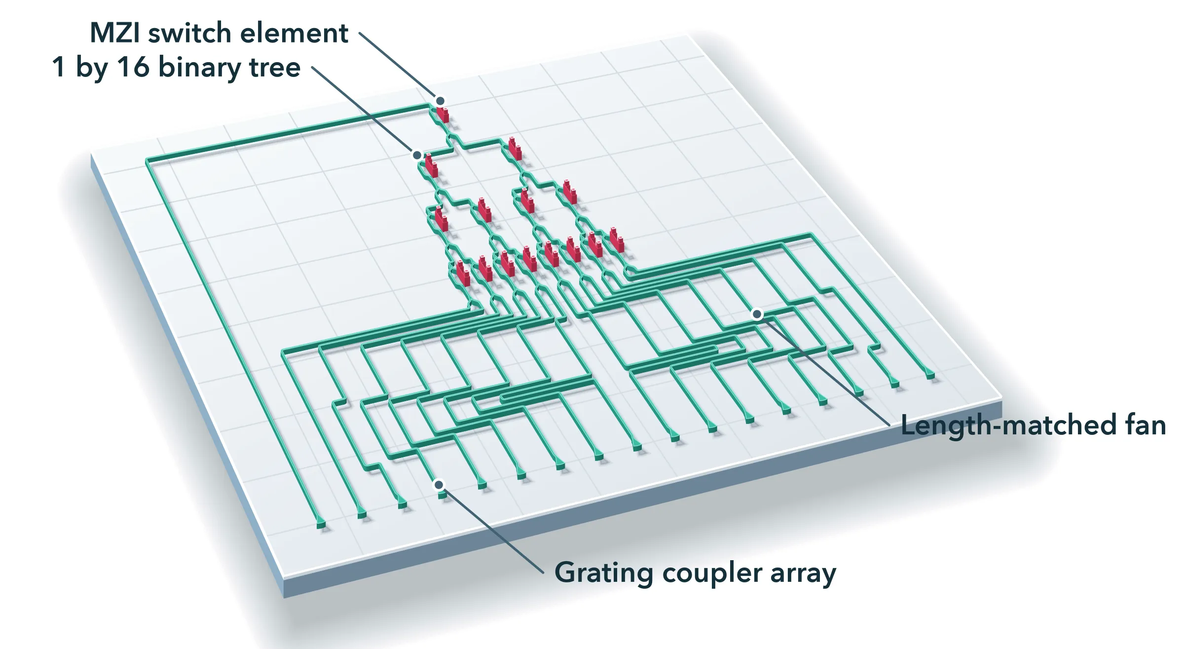
A 1 by N selector switch sends the light of one input to any one of N outputs. It is built as a binary tree of 1 by 2 switching elements: N - 1 elements in log2(N) stages, with exactly one element per stage on any path from the input to an output. That is the tree architecture of Spanke [1], and it is still the building block of silicon photonic switch fabrics: a strictly non-blocking N by N fabric is N of these trees feeding N mirrored combining trees [2].
Each element is a Mach-Zehnder interferometer with a thermo-optic phase shifter on one arm [3]. The tree points down, toward a single fiber array below it on the 127 μm pitch a fiber array is built to: one channel for the input and one per output.
Every route is drawn by route_auto with plain 90 degree corners. The question of this example is what path length matching does to the layout, so the same 1 by 16 selector, with every element in the same place, is routed twice:
- Auto routing:
route_autoroutes the whole selector, and the fan that joins the tree to the fibers ends up with channels of different lengths. - With matching: the fan asks for path length matching, and the router adds meanders to the short channels until every channel has the same length.
Each case prints its routing time and shows its layout.
References
- Spanke, Ronald A. “Architectures for guided-wave optical space switching systems.” IEEE Communications Magazine 1987 25 (5), 42-48, doi: 10.1109/MCOM.1987.1093615.
- Lee, Benjamin G., and Nicolas Dupuis. “Silicon photonic switch fabrics: technology and architecture.” Journal of Lightwave Technology 2019 37 (1), 6-20, doi: 10.1109/JLT.2018.2876828.
- Harris, Nicholas C., et al. “Efficient, compact and low loss thermo-optic phase shifter in silicon.” Optics Express 2014 22 (9), 10487-10493, doi: 10.1364/OE.22.010487.
- Chrostowski, Lukas, et al. “Silicon photonic circuit design using rapid prototyping foundry process design kits.” IEEE Journal of Selected Topics in Quantum Electronics 2019 25 (5), 8201326, doi: 10.1109/JSTQE.2019.2917501.
Setting up
Section titled “Setting up”The SiEPIC OpenEBL technology [4] is loaded through the siepic_forge module. Every parametric call in this example inherits the default arguments below, so the elements and the routes that connect them are built in one waveguide type: a 500 nm wide silicon strip that guides the TE mode at 1550 nm. The bend radius is 10 μm everywhere.
import jsonimport time
import photonforge as pfimport siepic_forge as siepic
# Use the SiEPIC OpenEBL technology for every component in this examplepf.config.default_technology = siepic.ebeam()
bend_radius = 10.0  # Bend radius of the elements and of every route (μm)euler_fraction = 0.5  # Fraction of each bend drawn as an Euler curve
# Set the default arguments shared by all parametric calls belowpf.config.default_kwargs = {    "port_spec": "TE_1550_500",  # Port specification of the waveguides    "radius": bend_radius,  # Bend radius (μm)    "euler_fraction": euler_fraction,  # Fraction of each bend drawn as Euler curve}
# Hide port and label text so the layout views stay unclutteredpf.config.svg_labels = False
# Start the live viewer that displays the layoutsviewer = pf.live_viewer.LiveViewer()
LiveViewer started at http://127.0.0.1:38781. Call its 'stop()' method to free the port.The switching element
Section titled “The switching element”Three cells come from the PDK: a Y branch, which splits the light at the input of each element, a 2 by 2 broadband directional coupler, which recombines it at the output, and a TE grating coupler for the fiber array.
The element is a Mach-Zehnder interferometer with one heated arm. Light entering P0 is
split in two, the heater sets the relative phase of the arms, and the coupler sends the
result to P1 or to P2 according to that phase. Both arms are the same length, so the
element is balanced when the heater is off.
The two outputs of the coupler are only 4.7 μm apart, closer than the router can separate two waveguides. A pair of S bends spreads them to 40 μm, the output pitch of the tree, so the outputs of one element are spaced exactly like the outputs of two neighboring elements.
The heater is a resistive strip on the M1_heater layer with a contact on M2_router at
either end, registered as terminals. Each contact sits
on an M1_heater patch that extends 3 μm past it on every side, which is the overlap the
design rules ask for. For the optical routing, both metal layers are blockers.
# Load the Y branch, which splits the light at the input of each elementy_branch = siepic.component("ebeam_y_1550")
# Load the 2 by 2 broadband directional coupler, which recombines the armscoupler = siepic.component("ebeam_bdc_te1550")
# Load the TE grating coupler used for the fiber arraygrating = siepic.component("ebeam_gc_te1550")
# Measure the spacing between the two output ports of the Y branch (μm)y_pitch = y_branch["P2"].center[1] - y_branch["P1"].center[1]
# Measure the spacing between the two output ports of the coupler (μm)coupler_pitch = coupler["P3"].center[1] - coupler["P2"].center[1]
fiber_pitch = 127.0  # Pitch of a standard single mode fiber array (μm)output_pitch = 40.0  # Spacing between adjacent outputs of the tree (μm)arm_bend_length = 25.0  # Length of the S bends that open and close the arms (μm)fan_bend_length = 40.0  # Length of the S bends that spread the outputs (μm)contact_margin = 3.0  # Distance the M1 patch extends past each M2 contact (μm)
switch_element builds one element from these three cells. Its arguments set the length of
the two arms, the distance between them, the width of the heater strip, and the side of
each contact. The defaults give an element 236 μm long and 52 μm wide. The S bends that
open and close the arms are 25 μm long, and those that spread the outputs are 40 μm long.
# Define the switching element as a parametric component@pf.parametric_componentdef switch_element(    *,    arm_length=60.0,  # Length of the straight section of each arm (μm)    arm_separation=30.0,  # Distance between the two arms (μm)    heater_width=3.0,  # Width of the heater strip (μm)    contact_size=12.0,  # Side length of each square heater contact (μm)):    # Create the parent component of the element    element = pf.Component()
    # Add the Y branch that splits the input light    split = element.add_reference(y_branch)
    # Calculate the offset of the S bends after the Y branch (μm)    split_offset = arm_separation / 2 - y_pitch / 2
    # Calculate the offset of the S bends before the coupler (μm)    merge_offset = arm_separation / 2 - coupler_pitch / 2
    # Create the S bend that opens the upper arm after the Y branch    up_in = pf.parametric.s_bend(length=arm_bend_length, offset=split_offset)
    # Create the S bend that opens the lower arm after the Y branch    down_in = pf.parametric.s_bend(length=arm_bend_length, offset=-split_offset)
    # Create the S bend that closes the lower arm before the coupler    up_out = pf.parametric.s_bend(length=arm_bend_length, offset=merge_offset)
    # Create the S bend that closes the upper arm before the coupler    down_out = pf.parametric.s_bend(length=arm_bend_length, offset=-merge_offset)
    # Create the straight section shared by both arms    arm = pf.parametric.straight(length=arm_length)
    # Open the upper arm, the one the heater sits on, add its straight section, and close it    # toward the coupler    upper = pf.reference_chain(        {"open": up_in, "arm": arm, "close": down_out}, "open - arm - close", start=split["P2"]    )    element.add(*upper)    _, heated, upper_out = upper
    # Read the start and end of the heated section for the heater strip    (x_start, y_strip), (x_stop, _) = heated["P0"].center, heated["P1"].center
    # Build the lower arm the same way, with no heater and as long as the upper one    lower = pf.reference_chain(        {"open": down_in, "arm": arm, "close": up_out}, "open - arm - close", start=split["P1"]    )    element.add(*lower)    # Add the coupler, connected to the upper arm so it also aligns with the lower one    combine = element.add_reference(coupler).connect("P1", upper_out["P1"])
    # Calculate the offset of the S bends that spread the outputs (μm)    fan_offset = output_pitch / 2 - coupler_pitch / 2
    # Create the S bend that spreads the lower coupler output    low_bend = pf.parametric.s_bend(length=fan_bend_length, offset=-fan_offset)
    # Add the S bend to the element    low = element.add_reference(low_bend)
    # Connect the S bend to the lower coupler output    low.connect("P0", combine["P2"])
    # Create the S bend that spreads the upper coupler output    high_bend = pf.parametric.s_bend(length=fan_bend_length, offset=fan_offset)
    # Add the S bend to the element    high = element.add_reference(high_bend)
    # Connect the S bend to the upper coupler output    high.connect("P0", combine["P3"])
    # Create the heater strip along the upper arm    heater = pf.Rectangle(        (x_start, y_strip - heater_width / 2), (x_stop, y_strip + heater_width / 2)    )
    # Add the heater strip to the heater layer    element.add("M1_heater", heater)
    # Add one contact at each end of the heater    for i, x_contact in enumerate((x_start, x_stop)):        # Find the center of the contact, on the upper edge of the heater strip        center = (x_contact, y_strip + heater_width / 2 + contact_size / 2)
        # Create the M2 contact        contact = pf.Rectangle(center=center, size=(contact_size, contact_size))
        # Add the contact to the router layer        element.add("M2_router", contact)
        # Calculate the side of the larger M1 patch under the contact (μm)        patch_size = contact_size + 2 * contact_margin
        # Create the M1 patch under the contact        patch = pf.Rectangle(center=center, size=(patch_size, patch_size))
        # Add the patch to the heater layer        element.add("M1_heater", patch)
        # Register the contact as an electrical terminal        element.add_terminal(pf.Terminal("M2_router", contact), f"T{i}")
    # Expose the input and the two outputs: P0 input, P1 lower output, P2 upper output    element.add_port([split["P0"], low["P1"], high["P1"]])
    # Attach a circuit model so the element can be simulated later    element.add_model(pf.CircuitModel(), "Circuit")    return element
The cell below creates one element with the default dimensions and shows it in the viewer.
# Create one switching element with the default dimensionselement = switch_element()
# Show the element in the viewerviewer(element);fill:%23221f20;font-weight:bold;font-size:3.032600px;}.terminal{fill:none;stroke:%23805080;stroke-width:0.379075;}.dashed{stroke-dasharray:1.895375,1.137225;}.port{fill:none;stroke:%23805080;stroke-width:0.758150;}.virtual-connection{fill:none;stroke:%23907090;stroke-width:0.568612;}.layer_31_0{stroke:%238c78ef;fill:url(%23pat-layer_31_0);fill-opacity:0.492;}.label_31_0{fill:%238c78ef;}.layer_33_0{stroke:%238c78ef;fill:url(%23pat-layer_33_0);fill-opacity:0.492;}.label_33_0{fill:%238c78ef;}.layer_102_0{stroke:%238c78ef;fill:url(%23pat-layer_102_0);fill-opacity:0.492;}.label_102_0{fill:%238c78ef;}.layer_110_0{stroke:%238c78ef;fill:url(%23pat-layer_110_0);fill-opacity:0.492;}.label_110_0{fill:%238c78ef;}.layer_189_0{stroke:%23000000;fill:none;}.label_189_0{fill:%23000000;}.layer_201_0{stroke:%2300ee00;fill:url(%23pat-layer_201_0);fill-opacity:0.492;}.label_201_0{fill:%2300ee00;}.layer_401_0{stroke:%236a8ad2;fill:url(%23pat-layer_401_0);fill-opacity:0.492;}.label_401_0{fill:%236a8ad2;}.layer_202_0{stroke:%23007600;fill:url(%23pat-layer_202_0);fill-opacity:0.492;}.label_202_0{fill:%23007600;}.layer_68_0{stroke:%23008000;fill:url(%23pat-layer_68_0);fill-opacity:0.492;}.label_68_0{fill:%23008000;}.layer_5_0{stroke:%236a8ad2;fill:url(%23pat-layer_5_0);fill-opacity:0.492;}.label_5_0{fill:%236a8ad2;}.layer_998_0{stroke:%23000000;fill:none;}.label_998_0{fill:%23000000;}.layer_312_1{stroke:%2300b8b8;fill:url(%23pat-layer_312_1);fill-opacity:0.492;}.label_312_1{fill:%2300b8b8;}.layer_312_0{stroke:%2300b8b8;fill:url(%23pat-layer_312_0);fill-opacity:0.492;}.label_312_0{fill:%2300b8b8;}.layer_402_0{stroke:%23ff0000;fill:url(%23pat-layer_402_0);fill-opacity:0.492;}.label_402_0{fill:%23ff0000;}.layer_401_4{stroke:%236a8ad2;fill:url(%23pat-layer_401_4);fill-opacity:0.492;}.label_401_4{fill:%236a8ad2;}.layer_389_0{stroke:%23ff00ff;fill:url(%23pat-layer_389_0);fill-opacity:0.492;}.label_389_0{fill:%23ff00ff;}.layer_402_1{stroke:%23ff0000;fill:url(%23pat-layer_402_1);fill-opacity:0.492;}.label_402_1{fill:%23ff0000;}.layer_350_1{stroke:%23697a00;fill:url(%23pat-layer_350_1);fill-opacity:0.492;}.label_350_1{fill:%23697a00;}.layer_401_1{stroke:%236a8ad2;fill:url(%23pat-layer_401_1);fill-opacity:0.492;}.label_401_1{fill:%236a8ad2;}.layer_313_2{stroke:%2301d95b;fill:url(%23pat-layer_313_2);fill-opacity:0.492;}.label_313_2{fill:%2301d95b;}.layer_313_1{stroke:%2301d95b;fill:url(%23pat-layer_313_1);fill-opacity:0.492;}.label_313_1{fill:%2301d95b;}.layer_313_0{stroke:%2301d95b;fill:url(%23pat-layer_313_0);fill-opacity:0.492;}.label_313_0{fill:%2301d95b;}.layer_400_0{stroke:%23a96868;fill:url(%23pat-layer_400_0);fill-opacity:0.492;}.label_400_0{fill:%23a96868;}.layer_312_3{stroke:%2300b8b8;fill:url(%23pat-layer_312_3);fill-opacity:0.492;}.label_312_3{fill:%2300b8b8;}.layer_389_1{stroke:%23ff00ff;fill:url(%23pat-layer_389_1);fill-opacity:0.492;}.label_389_1{fill:%23ff00ff;}.layer_401_3{stroke:%236a8ad2;fill:url(%23pat-layer_401_3);fill-opacity:0.492;}.label_401_3{fill:%236a8ad2;}.layer_403_2{stroke:%23500080;fill:url(%23pat-layer_403_2);fill-opacity:0.492;}.label_403_2{fill:%23500080;}.layer_403_3{stroke:%23500080;fill:url(%23pat-layer_403_3);fill-opacity:0.492;}.label_403_3{fill:%23500080;}.layer_403_1{stroke:%23500080;fill:url(%23pat-layer_403_1);fill-opacity:0.492;}.label_403_1{fill:%23500080;}.layer_403_0{stroke:%23500080;fill:url(%23pat-layer_403_0);fill-opacity:0.492;}.label_403_0{fill:%23500080;}.layer_311_1{stroke:%23ac6c56;fill:url(%23pat-layer_311_1);fill-opacity:0.492;}.label_311_1{fill:%23ac6c56;}.layer_311_0{stroke:%23ac6c56;fill:url(%23pat-layer_311_0);fill-opacity:0.492;}.label_311_0{fill:%23ac6c56;}.layer_301_1{stroke:%23800057;fill:url(%23pat-layer_301_1);fill-opacity:0.492;}.label_301_1{fill:%23800057;}.layer_301_0{stroke:%23800057;fill:url(%23pat-layer_301_0);fill-opacity:0.492;}.label_301_0{fill:%23800057;}.layer_305_1{stroke:%23808080;fill:url(%23pat-layer_305_1);fill-opacity:0.492;}.label_305_1{fill:%23808080;}.layer_305_0{stroke:%23808080;fill:url(%23pat-layer_305_0);fill-opacity:0.492;}.label_305_0{fill:%23808080;}.layer_999_0{stroke:%230000ff;fill:url(%23pat-layer_999_0);fill-opacity:0.492;}.label_999_0{fill:%230000ff;}.layer_81_0{stroke:%23808080;fill:url(%23pat-layer_81_0);fill-opacity:0.492;}.label_81_0{fill:%23808080;}.layer_290_0{stroke:%23a46eda;fill:none;}.label_290_0{fill:%23a46eda;}.layer_205_0{stroke:%2349b203;fill:url(%23pat-layer_205_0);fill-opacity:0.492;}.label_205_0{fill:%2349b203;}.layer_11_0{stroke:%230000ff;fill:url(%23pat-layer_11_0);fill-opacity:0.492;}.label_11_0{fill:%230000ff;}.layer_12_0{stroke:%23a57b00;fill:url(%23pat-layer_12_0);fill-opacity:0.492;}.label_12_0{fill:%23a57b00;}.layer_13_0{stroke:%23800057;fill:url(%23pat-layer_13_0);fill-opacity:0.492;}.label_13_0{fill:%23800057;}.layer_6_0{stroke:%23ff0000;fill:url(%23pat-layer_6_0);fill-opacity:0.492;}.label_6_0{fill:%23ff0000;}.layer_1_10{stroke:%23c96585;fill:url(%23pat-layer_1_10);fill-opacity:0.492;}.label_1_10{fill:%23c96585;}.layer_1_11{stroke:%23800000;fill:url(%23pat-layer_1_11);fill-opacity:0.492;}.label_1_11{fill:%23800000;}.layer_200_0{stroke:%23ff0000;fill:url(%23pat-layer_200_0);fill-opacity:0.492;}.label_200_0{fill:%23ff0000;}.layer_1_0{stroke:%23c96585;fill:url(%23pat-layer_1_0);fill-opacity:0.492;}.label_1_0{fill:%23c96585;}.layer_2_0{stroke:%23a46eda;fill:url(%23pat-layer_2_0);fill-opacity:0.492;}.label_2_0{fill:%23a46eda;}.layer_20_0{stroke:%2353793d;fill:url(%23pat-layer_20_0);fill-opacity:0.492;}.label_20_0{fill:%2353793d;}.layer_22_0{stroke:%23ec7600;fill:url(%23pat-layer_22_0);fill-opacity:0.492;}.label_22_0{fill:%23ec7600;}.layer_24_0{stroke:%2300b8b8;fill:url(%23pat-layer_24_0);fill-opacity:0.492;}.label_24_0{fill:%2300b8b8;}.layer_21_0{stroke:%23736264;fill:url(%23pat-layer_21_0);fill-opacity:0.492;}.label_21_0{fill:%23736264;}.layer_23_0{stroke:%23697a00;fill:url(%23pat-layer_23_0);fill-opacity:0.492;}.label_23_0{fill:%23697a00;}.layer_25_0{stroke:%23008000;fill:url(%23pat-layer_25_0);fill-opacity:0.492;}.label_25_0{fill:%23008000;}.layer_350_0{stroke:%23697a00;fill:url(%23pat-layer_350_0);fill-opacity:0.492;}.label_350_0{fill:%23697a00;}.layer_10_0{stroke:%23000000;fill:none;}.label_10_0{fill:%23000000;}.layer_203_0{stroke:%23008000;fill:url(%23pat-layer_203_0);fill-opacity:0.492;}.label_203_0{fill:%23008000;}.layer_40_0{stroke:%230000ff;fill:url(%23pat-layer_40_0);fill-opacity:0.492;}.label_40_0{fill:%230000ff;}.layer_401_2{stroke:%236a8ad2;fill:url(%23pat-layer_401_2);fill-opacity:0.492;}.label_401_2{fill:%236a8ad2;}.layer_301_2{stroke:%23800057;fill:url(%23pat-layer_301_2);fill-opacity:0.492;}.label_301_2{fill:%23800057;}</style><defs><path id=%22port-symbol%22 class=%22port%22 d=%22M 0,-1.516300 L 2.274450,0 0,1.516300%22 /><path id=%22ref-port-symbol%22 class=%22port%22 style=%22stroke-opacity:0.33;%22 d=%22M 0,-1.137225 C 1.516300,-1.137225 1.516300,1.137225 0,1.137225%22 /><circle id=%22port-bend-symbol%22 style=%22stroke-width:0;stroke:none;fill:%23805080;fill-opacity:1;%22 cx=%220%22 cy=%220%22 r=%220.682335%22 /><circle id=%22connection-symbol%22 style=%22stroke-width:0;stroke:none;fill:%23907090;fill-opacity:1;%22 cx=%220%22 cy=%220%22 r=%220.796057%22 /><pattern id=%22pat-layer_31_0%22 patternUnits=%22userSpaceOnUse%22 width=%221.895375%22 height=%221.895375%22 patternTransform=%22translate(1.449404,1.795618)%22><line x1=%220%22 y1=%220%22 x2=%221.895375%22 y2=%221.895375%22 style=%22stroke:%238c78ef;stroke-width:0.189537%22 /><line x1=%22-0.947688%22 y1=%220.947688%22 x2=%220.947688%22 y2=%222.843063%22 style=%22stroke:%238c78ef;stroke-width:0.189537%22 /><line x1=%220.947688%22 y1=%22-0.947688%22 x2=%222.843063%22 y2=%220.947688%22 style=%22stroke:%238c78ef;stroke-width:0.189537%22 /></pattern><pattern id=%22pat-layer_33_0%22 patternUnits=%22userSpaceOnUse%22 width=%221.895375%22 height=%221.895375%22 patternTransform=%22translate(1.114926,0.199513)%22><line x1=%220%22 y1=%220%22 x2=%221.895375%22 y2=%221.895375%22 style=%22stroke:%238c78ef;stroke-width:0.189537%22 /><line x1=%22-0.947688%22 y1=%220.947688%22 x2=%220.947688%22 y2=%222.843063%22 style=%22stroke:%238c78ef;stroke-width:0.189537%22 /><line x1=%220.947688%22 y1=%22-0.947688%22 x2=%222.843063%22 y2=%220.947688%22 style=%22stroke:%238c78ef;stroke-width:0.189537%22 /></pattern><pattern id=%22pat-layer_102_0%22 patternUnits=%22userSpaceOnUse%22 width=%221.895375%22 height=%221.895375%22 patternTransform=%22translate(0.000000,0.099757)%22><line x1=%220%22 y1=%220%22 x2=%221.895375%22 y2=%221.895375%22 style=%22stroke:%238c78ef;stroke-width:0.189537%22 /><line x1=%22-0.947688%22 y1=%220.947688%22 x2=%220.947688%22 y2=%222.843063%22 style=%22stroke:%238c78ef;stroke-width:0.189537%22 /><line x1=%220.947688%22 y1=%22-0.947688%22 x2=%222.843063%22 y2=%220.947688%22 style=%22stroke:%238c78ef;stroke-width:0.189537%22 /></pattern><pattern id=%22pat-layer_110_0%22 patternUnits=%22userSpaceOnUse%22 width=%221.895375%22 height=%221.895375%22 patternTransform=%22translate(0.557463,1.296836)%22><line x1=%220%22 y1=%220%22 x2=%221.895375%22 y2=%221.895375%22 style=%22stroke:%238c78ef;stroke-width:0.189537%22 /><line x1=%22-0.947688%22 y1=%220.947688%22 x2=%220.947688%22 y2=%222.843063%22 style=%22stroke:%238c78ef;stroke-width:0.189537%22 /><line x1=%220.947688%22 y1=%22-0.947688%22 x2=%222.843063%22 y2=%220.947688%22 style=%22stroke:%238c78ef;stroke-width:0.189537%22 /></pattern><pattern id=%22pat-layer_201_0%22 patternUnits=%22userSpaceOnUse%22 width=%221.895375%22 height=%221.895375%22 patternTransform=%22translate(1.449404,0.698296)%22><circle cx=%220.947688%22 cy=%220.947688%22 r=%220.189537%22 style=%22stroke:none;fill:%2300ee00;fill-opacity:1.0%22 /></pattern><pattern id=%22pat-layer_401_0%22 patternUnits=%22userSpaceOnUse%22 width=%221.137225%22 height=%221.137225%22 patternTransform=%22translate(0.133791,0.179562)%22><line x1=%220%22 y1=%220%22 x2=%221.137225%22 y2=%221.137225%22 style=%22stroke:%236a8ad2;stroke-width:0.189537%22 /><line x1=%22-0.568612%22 y1=%220.568612%22 x2=%220.568612%22 y2=%221.705837%22 style=%22stroke:%236a8ad2;stroke-width:0.189537%22 /><line x1=%220.568612%22 y1=%22-0.568612%22 x2=%221.705837%22 y2=%220.568612%22 style=%22stroke:%236a8ad2;stroke-width:0.189537%22 /><line x1=%221.137225%22 y1=%220%22 x2=%220%22 y2=%221.137225%22 style=%22stroke:%236a8ad2;stroke-width:0.189537%22 /><line x1=%221.705837%22 y1=%220.568612%22 x2=%220.568612%22 y2=%221.705837%22 style=%22stroke:%236a8ad2;stroke-width:0.189537%22 /><line x1=%220.568612%22 y1=%22-0.568612%22 x2=%22-0.568612%22 y2=%220.568612%22 style=%22stroke:%236a8ad2;stroke-width:0.189537%22 /></pattern><pattern id=%22pat-layer_202_0%22 patternUnits=%22userSpaceOnUse%22 width=%221.137225%22 height=%221.137225%22 patternTransform=%22translate(0.200687,1.077371)%22><circle cx=%220.568612%22 cy=%220.568612%22 r=%220.189537%22 style=%22stroke:none;fill:%23007600;fill-opacity:1.0%22 /></pattern><pattern id=%22pat-layer_68_0%22 patternUnits=%22userSpaceOnUse%22 width=%221.895375%22 height=%221.895375%22 patternTransform=%22translate(0.000000,0.698296)%22><circle cx=%220.947688%22 cy=%220.947688%22 r=%220.189537%22 style=%22stroke:none;fill:%23008000;fill-opacity:1.0%22 /></pattern><pattern id=%22pat-layer_5_0%22 patternUnits=%22userSpaceOnUse%22 width=%221.137225%22 height=%221.137225%22 patternTransform=%22translate(0.066896,1.017517)%22><line x1=%220.568612%22 y1=%220%22 x2=%220.568612%22 y2=%221.137225%22 style=%22stroke:%236a8ad2;stroke-width:0.189537%22 /></pattern><pattern id=%22pat-layer_312_1%22 patternUnits=%22userSpaceOnUse%22 width=%221.137225%22 height=%221.137225%22 patternTransform=%22translate(0.267582,0.897809)%22><line x1=%220%22 y1=%220%22 x2=%221.137225%22 y2=%221.137225%22 style=%22stroke:%2300b8b8;stroke-width:0.189537%22 /><line x1=%22-0.568612%22 y1=%220.568612%22 x2=%220.568612%22 y2=%221.705837%22 style=%22stroke:%2300b8b8;stroke-width:0.189537%22 /><line x1=%220.568612%22 y1=%22-0.568612%22 x2=%221.705837%22 y2=%220.568612%22 style=%22stroke:%2300b8b8;stroke-width:0.189537%22 /></pattern><pattern id=%22pat-layer_312_0%22 patternUnits=%22userSpaceOnUse%22 width=%221.895375%22 height=%221.895375%22 patternTransform=%22translate(0.891941,1.197079)%22><line x1=%220.947688%22 y1=%220%22 x2=%220.947688%22 y2=%221.895375%22 style=%22stroke:%2300b8b8;stroke-width:0.189537%22 /></pattern><pattern id=%22pat-layer_402_0%22 patternUnits=%22userSpaceOnUse%22 width=%221.895375%22 height=%221.895375%22 patternTransform=%22translate(1.003434,1.396592)%22><line x1=%220.947688%22 y1=%220%22 x2=%220.947688%22 y2=%221.895375%22 style=%22stroke:%23ff0000;stroke-width:0.189537%22 /><line x1=%220%22 y1=%220.947688%22 x2=%221.895375%22 y2=%220.947688%22 style=%22stroke:%23ff0000;stroke-width:0.189537%22 /></pattern><pattern id=%22pat-layer_401_4%22 patternUnits=%22userSpaceOnUse%22 width=%221.137225%22 height=%221.137225%22 patternTransform=%22translate(0.200687,0.897809)%22><line x1=%220.568612%22 y1=%220%22 x2=%220.568612%22 y2=%221.137225%22 style=%22stroke:%236a8ad2;stroke-width:0.189537%22 /></pattern><pattern id=%22pat-layer_389_0%22 patternUnits=%22userSpaceOnUse%22 width=%221.137225%22 height=%221.137225%22 patternTransform=%22translate(0.200687,0.239416)%22><line x1=%220.568612%22 y1=%220%22 x2=%220.568612%22 y2=%221.137225%22 style=%22stroke:%23ff00ff;stroke-width:0.189537%22 /><line x1=%220%22 y1=%220.568612%22 x2=%221.137225%22 y2=%220.568612%22 style=%22stroke:%23ff00ff;stroke-width:0.189537%22 /></pattern><pattern id=%22pat-layer_402_1%22 patternUnits=%22userSpaceOnUse%22 width=%221.137225%22 height=%221.137225%22 patternTransform=%22translate(0.334478,1.017517)%22><line x1=%220%22 y1=%220%22 x2=%221.137225%22 y2=%221.137225%22 style=%22stroke:%23ff0000;stroke-width:0.189537%22 /><line x1=%22-0.568612%22 y1=%220.568612%22 x2=%220.568612%22 y2=%221.705837%22 style=%22stroke:%23ff0000;stroke-width:0.189537%22 /><line x1=%220.568612%22 y1=%22-0.568612%22 x2=%221.705837%22 y2=%220.568612%22 style=%22stroke:%23ff0000;stroke-width:0.189537%22 /><line x1=%221.137225%22 y1=%220%22 x2=%220%22 y2=%221.137225%22 style=%22stroke:%23ff0000;stroke-width:0.189537%22 /><line x1=%221.705837%22 y1=%220.568612%22 x2=%220.568612%22 y2=%221.705837%22 style=%22stroke:%23ff0000;stroke-width:0.189537%22 /><line x1=%220.568612%22 y1=%22-0.568612%22 x2=%22-0.568612%22 y2=%220.568612%22 style=%22stroke:%23ff0000;stroke-width:0.189537%22 /></pattern><pattern id=%22pat-layer_350_1%22 patternUnits=%22userSpaceOnUse%22 width=%221.137225%22 height=%221.137225%22 patternTransform=%22translate(1.003434,0.897809)%22><circle cx=%220.568612%22 cy=%220.568612%22 r=%220.189537%22 style=%22stroke:none;fill:%23697a00;fill-opacity:1.0%22 /></pattern><pattern id=%22pat-layer_401_1%22 patternUnits=%22userSpaceOnUse%22 width=%221.895375%22 height=%221.895375%22 patternTransform=%22translate(1.672390,0.598539)%22><line x1=%220%22 y1=%220%22 x2=%221.895375%22 y2=%221.895375%22 style=%22stroke:%236a8ad2;stroke-width:0.189537%22 /><line x1=%22-0.947688%22 y1=%220.947688%22 x2=%220.947688%22 y2=%222.843063%22 style=%22stroke:%236a8ad2;stroke-width:0.189537%22 /><line x1=%220.947688%22 y1=%22-0.947688%22 x2=%222.843063%22 y2=%220.947688%22 style=%22stroke:%236a8ad2;stroke-width:0.189537%22 /><line x1=%221.895375%22 y1=%220%22 x2=%220%22 y2=%221.895375%22 style=%22stroke:%236a8ad2;stroke-width:0.189537%22 /><line x1=%222.843063%22 y1=%220.947688%22 x2=%220.947688%22 y2=%222.843063%22 style=%22stroke:%236a8ad2;stroke-width:0.189537%22 /><line x1=%220.947688%22 y1=%22-0.947688%22 x2=%22-0.947688%22 y2=%220.947688%22 style=%22stroke:%236a8ad2;stroke-width:0.189537%22 /></pattern><pattern id=%22pat-layer_313_2%22 patternUnits=%22userSpaceOnUse%22 width=%221.137225%22 height=%221.137225%22 patternTransform=%22translate(0.468269,0.598539)%22><line x1=%220%22 y1=%220%22 x2=%221.137225%22 y2=%221.137225%22 style=%22stroke:%2301d95b;stroke-width:0.189537%22 /><line x1=%22-0.568612%22 y1=%220.568612%22 x2=%220.568612%22 y2=%221.705837%22 style=%22stroke:%2301d95b;stroke-width:0.189537%22 /><line x1=%220.568612%22 y1=%22-0.568612%22 x2=%221.705837%22 y2=%220.568612%22 style=%22stroke:%2301d95b;stroke-width:0.189537%22 /></pattern><pattern id=%22pat-layer_313_1%22 patternUnits=%22userSpaceOnUse%22 width=%221.895375%22 height=%221.895375%22 patternTransform=%22translate(1.226419,0.698296)%22><line x1=%220.947688%22 y1=%220%22 x2=%220.947688%22 y2=%221.895375%22 style=%22stroke:%2301d95b;stroke-width:0.189537%22 /></pattern><pattern id=%22pat-layer_313_0%22 patternUnits=%22userSpaceOnUse%22 width=%221.137225%22 height=%221.137225%22 patternTransform=%22translate(1.003434,0.239416)%22><line x1=%220.568612%22 y1=%220%22 x2=%220.568612%22 y2=%221.137225%22 style=%22stroke:%2301d95b;stroke-width:0.189537%22 /></pattern><pattern id=%22pat-layer_400_0%22 patternUnits=%22userSpaceOnUse%22 width=%221.895375%22 height=%221.895375%22 patternTransform=%22translate(1.337912,1.097322)%22><line x1=%220%22 y1=%220%22 x2=%221.895375%22 y2=%221.895375%22 style=%22stroke:%23a96868;stroke-width:0.189537%22 /><line x1=%22-0.947688%22 y1=%220.947688%22 x2=%220.947688%22 y2=%222.843063%22 style=%22stroke:%23a96868;stroke-width:0.189537%22 /><line x1=%220.947688%22 y1=%22-0.947688%22 x2=%222.843063%22 y2=%220.947688%22 style=%22stroke:%23a96868;stroke-width:0.189537%22 /><line x1=%221.895375%22 y1=%220%22 x2=%220%22 y2=%221.895375%22 style=%22stroke:%23a96868;stroke-width:0.189537%22 /><line x1=%222.843063%22 y1=%220.947688%22 x2=%220.947688%22 y2=%222.843063%22 style=%22stroke:%23a96868;stroke-width:0.189537%22 /><line x1=%220.947688%22 y1=%22-0.947688%22 x2=%22-0.947688%22 y2=%220.947688%22 style=%22stroke:%23a96868;stroke-width:0.189537%22 /></pattern><pattern id=%22pat-layer_312_3%22 patternUnits=%22userSpaceOnUse%22 width=%221.137225%22 height=%221.137225%22 patternTransform=%22translate(0.869643,0.119708)%22><line x1=%221.137225%22 y1=%220%22 x2=%220%22 y2=%221.137225%22 style=%22stroke:%2300b8b8;stroke-width:0.189537%22 /><line x1=%221.705837%22 y1=%220.568612%22 x2=%220.568612%22 y2=%221.705837%22 style=%22stroke:%2300b8b8;stroke-width:0.189537%22 /><line x1=%220.568612%22 y1=%22-0.568612%22 x2=%22-0.568612%22 y2=%220.568612%22 style=%22stroke:%2300b8b8;stroke-width:0.189537%22 /></pattern><pattern id=%22pat-layer_389_1%22 patternUnits=%22userSpaceOnUse%22 width=%221.895375%22 height=%221.895375%22 patternTransform=%22translate(1.783882,0.698296)%22><line x1=%220.947688%22 y1=%220%22 x2=%220.947688%22 y2=%221.895375%22 style=%22stroke:%23ff00ff;stroke-width:0.189537%22 /><line x1=%220%22 y1=%220.947688%22 x2=%221.895375%22 y2=%220.947688%22 style=%22stroke:%23ff00ff;stroke-width:0.189537%22 /></pattern><pattern id=%22pat-layer_401_3%22 patternUnits=%22userSpaceOnUse%22 width=%221.895375%22 height=%221.895375%22 patternTransform=%22translate(0.780449,1.197079)%22><line x1=%220%22 y1=%220.947688%22 x2=%221.895375%22 y2=%220.947688%22 style=%22stroke:%236a8ad2;stroke-width:0.189537%22 /></pattern><pattern id=%22pat-layer_403_2%22 patternUnits=%22userSpaceOnUse%22 width=%221.137225%22 height=%221.137225%22 patternTransform=%22translate(0.535165,0.718247)%22><line x1=%220%22 y1=%220%22 x2=%221.137225%22 y2=%221.137225%22 style=%22stroke:%23500080;stroke-width:0.189537%22 /><line x1=%22-0.568612%22 y1=%220.568612%22 x2=%220.568612%22 y2=%221.705837%22 style=%22stroke:%23500080;stroke-width:0.189537%22 /><line x1=%220.568612%22 y1=%22-0.568612%22 x2=%221.705837%22 y2=%220.568612%22 style=%22stroke:%23500080;stroke-width:0.189537%22 /><line x1=%221.137225%22 y1=%220%22 x2=%220%22 y2=%221.137225%22 style=%22stroke:%23500080;stroke-width:0.189537%22 /><line x1=%221.705837%22 y1=%220.568612%22 x2=%220.568612%22 y2=%221.705837%22 style=%22stroke:%23500080;stroke-width:0.189537%22 /><line x1=%220.568612%22 y1=%22-0.568612%22 x2=%22-0.568612%22 y2=%220.568612%22 style=%22stroke:%23500080;stroke-width:0.189537%22 /></pattern><pattern id=%22pat-layer_403_3%22 patternUnits=%22userSpaceOnUse%22 width=%221.895375%22 height=%221.895375%22 patternTransform=%22translate(0.445971,1.496349)%22><line x1=%220%22 y1=%220%22 x2=%221.895375%22 y2=%221.895375%22 style=%22stroke:%23500080;stroke-width:0.189537%22 /><line x1=%22-0.947688%22 y1=%220.947688%22 x2=%220.947688%22 y2=%222.843063%22 style=%22stroke:%23500080;stroke-width:0.189537%22 /><line x1=%220.947688%22 y1=%22-0.947688%22 x2=%222.843063%22 y2=%220.947688%22 style=%22stroke:%23500080;stroke-width:0.189537%22 /><line x1=%221.895375%22 y1=%220%22 x2=%220%22 y2=%221.895375%22 style=%22stroke:%23500080;stroke-width:0.189537%22 /><line x1=%222.843063%22 y1=%220.947688%22 x2=%220.947688%22 y2=%222.843063%22 style=%22stroke:%23500080;stroke-width:0.189537%22 /><line x1=%220.947688%22 y1=%22-0.947688%22 x2=%22-0.947688%22 y2=%220.947688%22 style=%22stroke:%23500080;stroke-width:0.189537%22 /></pattern><pattern id=%22pat-layer_403_1%22 patternUnits=%22userSpaceOnUse%22 width=%221.895375%22 height=%221.895375%22 patternTransform=%22translate(1.337912,0.897809)%22><line x1=%220.947688%22 y1=%220%22 x2=%220.947688%22 y2=%221.895375%22 style=%22stroke:%23500080;stroke-width:0.189537%22 /><line x1=%220%22 y1=%220.947688%22 x2=%221.895375%22 y2=%220.947688%22 style=%22stroke:%23500080;stroke-width:0.189537%22 /></pattern><pattern id=%22pat-layer_403_0%22 patternUnits=%22userSpaceOnUse%22 width=%221.137225%22 height=%221.137225%22 patternTransform=%22translate(1.070329,0.359124)%22><line x1=%220.568612%22 y1=%220%22 x2=%220.568612%22 y2=%221.137225%22 style=%22stroke:%23500080;stroke-width:0.189537%22 /><line x1=%220%22 y1=%220.568612%22 x2=%221.137225%22 y2=%220.568612%22 style=%22stroke:%23500080;stroke-width:0.189537%22 /></pattern><pattern id=%22pat-layer_311_1%22 patternUnits=%22userSpaceOnUse%22 width=%221.895375%22 height=%221.895375%22 patternTransform=%22translate(1.560897,0.399026)%22><line x1=%220%22 y1=%220%22 x2=%221.895375%22 y2=%221.895375%22 style=%22stroke:%23ac6c56;stroke-width:0.189537%22 /><line x1=%22-0.947688%22 y1=%220.947688%22 x2=%220.947688%22 y2=%222.843063%22 style=%22stroke:%23ac6c56;stroke-width:0.189537%22 /><line x1=%220.947688%22 y1=%22-0.947688%22 x2=%222.843063%22 y2=%220.947688%22 style=%22stroke:%23ac6c56;stroke-width:0.189537%22 /></pattern><pattern id=%22pat-layer_311_0%22 patternUnits=%22userSpaceOnUse%22 width=%221.137225%22 height=%221.137225%22 patternTransform=%22translate(0.066896,0.059854)%22><line x1=%220%22 y1=%220%22 x2=%221.137225%22 y2=%221.137225%22 style=%22stroke:%23ac6c56;stroke-width:0.189537%22 /><line x1=%22-0.568612%22 y1=%220.568612%22 x2=%220.568612%22 y2=%221.705837%22 style=%22stroke:%23ac6c56;stroke-width:0.189537%22 /><line x1=%220.568612%22 y1=%22-0.568612%22 x2=%221.705837%22 y2=%220.568612%22 style=%22stroke:%23ac6c56;stroke-width:0.189537%22 /></pattern><pattern id=%22pat-layer_301_1%22 patternUnits=%22userSpaceOnUse%22 width=%221.895375%22 height=%221.895375%22 patternTransform=%22translate(1.337912,0.798053)%22><line x1=%220%22 y1=%220.947688%22 x2=%221.895375%22 y2=%220.947688%22 style=%22stroke:%23800057;stroke-width:0.189537%22 /></pattern><pattern id=%22pat-layer_301_0%22 patternUnits=%22userSpaceOnUse%22 width=%221.137225%22 height=%221.137225%22 patternTransform=%22translate(1.070329,0.299270)%22><line x1=%220%22 y1=%220.568612%22 x2=%221.137225%22 y2=%220.568612%22 style=%22stroke:%23800057;stroke-width:0.189537%22 /></pattern><pattern id=%22pat-layer_305_1%22 patternUnits=%22userSpaceOnUse%22 width=%221.895375%22 height=%221.895375%22 patternTransform=%22translate(0.668956,1.396592)%22><line x1=%220.947688%22 y1=%220%22 x2=%220.947688%22 y2=%221.895375%22 style=%22stroke:%23808080;stroke-width:0.189537%22 /><line x1=%220%22 y1=%220.947688%22 x2=%221.895375%22 y2=%220.947688%22 style=%22stroke:%23808080;stroke-width:0.189537%22 /></pattern><pattern id=%22pat-layer_305_0%22 patternUnits=%22userSpaceOnUse%22 width=%221.137225%22 height=%221.137225%22 patternTransform=%22translate(0.668956,0.658393)%22><line x1=%220.568612%22 y1=%220%22 x2=%220.568612%22 y2=%221.137225%22 style=%22stroke:%23808080;stroke-width:0.189537%22 /><line x1=%220%22 y1=%220.568612%22 x2=%221.137225%22 y2=%220.568612%22 style=%22stroke:%23808080;stroke-width:0.189537%22 /></pattern><pattern id=%22pat-layer_999_0%22 patternUnits=%22userSpaceOnUse%22 width=%221.137225%22 height=%221.137225%22 patternTransform=%22translate(0.401374,0.418978)%22><line x1=%220.568612%22 y1=%220%22 x2=%220.568612%22 y2=%221.137225%22 style=%22stroke:%230000ff;stroke-width:0.189537%22 /></pattern><pattern id=%22pat-layer_81_0%22 patternUnits=%22userSpaceOnUse%22 width=%221.137225%22 height=%221.137225%22 patternTransform=%22translate(0.401374,1.017517)%22><line x1=%220.568612%22 y1=%220%22 x2=%220.568612%22 y2=%221.137225%22 style=%22stroke:%23808080;stroke-width:0.189537%22 /><line x1=%220%22 y1=%220.568612%22 x2=%221.137225%22 y2=%220.568612%22 style=%22stroke:%23808080;stroke-width:0.189537%22 /></pattern><pattern id=%22pat-layer_205_0%22 patternUnits=%22userSpaceOnUse%22 width=%221.137225%22 height=%221.137225%22 patternTransform=%22translate(0.468269,0.778101)%22><line x1=%220%22 y1=%220%22 x2=%221.137225%22 y2=%221.137225%22 style=%22stroke:%2349b203;stroke-width:0.189537%22 /><line x1=%22-0.568612%22 y1=%220.568612%22 x2=%220.568612%22 y2=%221.705837%22 style=%22stroke:%2349b203;stroke-width:0.189537%22 /><line x1=%220.568612%22 y1=%22-0.568612%22 x2=%221.705837%22 y2=%220.568612%22 style=%22stroke:%2349b203;stroke-width:0.189537%22 /><line x1=%221.137225%22 y1=%220%22 x2=%220%22 y2=%221.137225%22 style=%22stroke:%2349b203;stroke-width:0.189537%22 /><line x1=%221.705837%22 y1=%220.568612%22 x2=%220.568612%22 y2=%221.705837%22 style=%22stroke:%2349b203;stroke-width:0.189537%22 /><line x1=%220.568612%22 y1=%22-0.568612%22 x2=%22-0.568612%22 y2=%220.568612%22 style=%22stroke:%2349b203;stroke-width:0.189537%22 /></pattern><pattern id=%22pat-layer_11_0%22 patternUnits=%22userSpaceOnUse%22 width=%221.137225%22 height=%221.137225%22 patternTransform=%22translate(0.602060,0.418978)%22><line x1=%221.137225%22 y1=%220%22 x2=%220%22 y2=%221.137225%22 style=%22stroke:%230000ff;stroke-width:0.189537%22 /><line x1=%221.705837%22 y1=%220.568612%22 x2=%220.568612%22 y2=%221.705837%22 style=%22stroke:%230000ff;stroke-width:0.189537%22 /><line x1=%220.568612%22 y1=%22-0.568612%22 x2=%22-0.568612%22 y2=%220.568612%22 style=%22stroke:%230000ff;stroke-width:0.189537%22 /></pattern><pattern id=%22pat-layer_12_0%22 patternUnits=%22userSpaceOnUse%22 width=%221.137225%22 height=%221.137225%22 patternTransform=%22translate(1.070329,1.077371)%22><line x1=%220%22 y1=%220%22 x2=%221.137225%22 y2=%221.137225%22 style=%22stroke:%23a57b00;stroke-width:0.189537%22 /><line x1=%22-0.568612%22 y1=%220.568612%22 x2=%220.568612%22 y2=%221.705837%22 style=%22stroke:%23a57b00;stroke-width:0.189537%22 /><line x1=%220.568612%22 y1=%22-0.568612%22 x2=%221.705837%22 y2=%220.568612%22 style=%22stroke:%23a57b00;stroke-width:0.189537%22 /></pattern><pattern id=%22pat-layer_13_0%22 patternUnits=%22userSpaceOnUse%22 width=%221.137225%22 height=%221.137225%22 patternTransform=%22translate(0.401374,0.598539)%22><line x1=%221.137225%22 y1=%220%22 x2=%220%22 y2=%221.137225%22 style=%22stroke:%23800057;stroke-width:0.189537%22 /><line x1=%221.705837%22 y1=%220.568612%22 x2=%220.568612%22 y2=%221.705837%22 style=%22stroke:%23800057;stroke-width:0.189537%22 /><line x1=%220.568612%22 y1=%22-0.568612%22 x2=%22-0.568612%22 y2=%220.568612%22 style=%22stroke:%23800057;stroke-width:0.189537%22 /></pattern><pattern id=%22pat-layer_6_0%22 patternUnits=%22userSpaceOnUse%22 width=%221.895375%22 height=%221.895375%22 patternTransform=%22translate(0.891941,0.897809)%22><line x1=%220%22 y1=%220.947688%22 x2=%221.895375%22 y2=%220.947688%22 style=%22stroke:%23ff0000;stroke-width:0.189537%22 /></pattern><pattern id=%22pat-layer_1_10%22 patternUnits=%22userSpaceOnUse%22 width=%221.137225%22 height=%221.137225%22 patternTransform=%22translate(0.066896,0.179562)%22><line x1=%220%22 y1=%220%22 x2=%221.137225%22 y2=%221.137225%22 style=%22stroke:%23c96585;stroke-width:0.189537%22 /><line x1=%22-0.568612%22 y1=%220.568612%22 x2=%220.568612%22 y2=%221.705837%22 style=%22stroke:%23c96585;stroke-width:0.189537%22 /><line x1=%220.568612%22 y1=%22-0.568612%22 x2=%221.705837%22 y2=%220.568612%22 style=%22stroke:%23c96585;stroke-width:0.189537%22 /><line x1=%221.137225%22 y1=%220%22 x2=%220%22 y2=%221.137225%22 style=%22stroke:%23c96585;stroke-width:0.189537%22 /><line x1=%221.705837%22 y1=%220.568612%22 x2=%220.568612%22 y2=%221.705837%22 style=%22stroke:%23c96585;stroke-width:0.189537%22 /><line x1=%220.568612%22 y1=%22-0.568612%22 x2=%22-0.568612%22 y2=%220.568612%22 style=%22stroke:%23c96585;stroke-width:0.189537%22 /></pattern><pattern id=%22pat-layer_1_11%22 patternUnits=%22userSpaceOnUse%22 width=%221.895375%22 height=%221.895375%22 patternTransform=%22translate(1.560897,0.598539)%22><line x1=%220.947688%22 y1=%220%22 x2=%220.947688%22 y2=%221.895375%22 style=%22stroke:%23800000;stroke-width:0.189537%22 /><line x1=%220%22 y1=%220.947688%22 x2=%221.895375%22 y2=%220.947688%22 style=%22stroke:%23800000;stroke-width:0.189537%22 /></pattern><pattern id=%22pat-layer_200_0%22 patternUnits=%22userSpaceOnUse%22 width=%221.895375%22 height=%221.895375%22 patternTransform=%22translate(0.668956,1.496349)%22><line x1=%220%22 y1=%220%22 x2=%221.895375%22 y2=%221.895375%22 style=%22stroke:%23ff0000;stroke-width:0.189537%22 /><line x1=%22-0.947688%22 y1=%220.947688%22 x2=%220.947688%22 y2=%222.843063%22 style=%22stroke:%23ff0000;stroke-width:0.189537%22 /><line x1=%220.947688%22 y1=%22-0.947688%22 x2=%222.843063%22 y2=%220.947688%22 style=%22stroke:%23ff0000;stroke-width:0.189537%22 /><line x1=%221.895375%22 y1=%220%22 x2=%220%22 y2=%221.895375%22 style=%22stroke:%23ff0000;stroke-width:0.189537%22 /><line x1=%222.843063%22 y1=%220.947688%22 x2=%220.947688%22 y2=%222.843063%22 style=%22stroke:%23ff0000;stroke-width:0.189537%22 /><line x1=%220.947688%22 y1=%22-0.947688%22 x2=%22-0.947688%22 y2=%220.947688%22 style=%22stroke:%23ff0000;stroke-width:0.189537%22 /></pattern><pattern id=%22pat-layer_1_0%22 patternUnits=%22userSpaceOnUse%22 width=%221.137225%22 height=%221.137225%22 patternTransform=%22translate(0.468269,0.658393)%22><line x1=%221.137225%22 y1=%220%22 x2=%220%22 y2=%221.137225%22 style=%22stroke:%23c96585;stroke-width:0.189537%22 /><line x1=%221.705837%22 y1=%220.568612%22 x2=%220.568612%22 y2=%221.705837%22 style=%22stroke:%23c96585;stroke-width:0.189537%22 /><line x1=%220.568612%22 y1=%22-0.568612%22 x2=%22-0.568612%22 y2=%220.568612%22 style=%22stroke:%23c96585;stroke-width:0.189537%22 /></pattern><pattern id=%22pat-layer_2_0%22 patternUnits=%22userSpaceOnUse%22 width=%221.895375%22 height=%221.895375%22 patternTransform=%22translate(1.560897,0.299270)%22><line x1=%220%22 y1=%220%22 x2=%221.895375%22 y2=%221.895375%22 style=%22stroke:%23a46eda;stroke-width:0.189537%22 /><line x1=%22-0.947688%22 y1=%220.947688%22 x2=%220.947688%22 y2=%222.843063%22 style=%22stroke:%23a46eda;stroke-width:0.189537%22 /><line x1=%220.947688%22 y1=%22-0.947688%22 x2=%222.843063%22 y2=%220.947688%22 style=%22stroke:%23a46eda;stroke-width:0.189537%22 /></pattern><pattern id=%22pat-layer_20_0%22 patternUnits=%22userSpaceOnUse%22 width=%221.895375%22 height=%221.895375%22 patternTransform=%22translate(0.445971,1.097322)%22><line x1=%220%22 y1=%220.947688%22 x2=%221.895375%22 y2=%220.947688%22 style=%22stroke:%2353793d;stroke-width:0.189537%22 /></pattern><pattern id=%22pat-layer_22_0%22 patternUnits=%22userSpaceOnUse%22 width=%221.895375%22 height=%221.895375%22 patternTransform=%22translate(0.111493,1.396592)%22><line x1=%220%22 y1=%220%22 x2=%221.895375%22 y2=%221.895375%22 style=%22stroke:%23ec7600;stroke-width:0.189537%22 /><line x1=%22-0.947688%22 y1=%220.947688%22 x2=%220.947688%22 y2=%222.843063%22 style=%22stroke:%23ec7600;stroke-width:0.189537%22 /><line x1=%220.947688%22 y1=%22-0.947688%22 x2=%222.843063%22 y2=%220.947688%22 style=%22stroke:%23ec7600;stroke-width:0.189537%22 /><line x1=%221.895375%22 y1=%220%22 x2=%220%22 y2=%221.895375%22 style=%22stroke:%23ec7600;stroke-width:0.189537%22 /><line x1=%222.843063%22 y1=%220.947688%22 x2=%220.947688%22 y2=%222.843063%22 style=%22stroke:%23ec7600;stroke-width:0.189537%22 /><line x1=%220.947688%22 y1=%22-0.947688%22 x2=%22-0.947688%22 y2=%220.947688%22 style=%22stroke:%23ec7600;stroke-width:0.189537%22 /></pattern><pattern id=%22pat-layer_24_0%22 patternUnits=%22userSpaceOnUse%22 width=%221.895375%22 height=%221.895375%22 patternTransform=%22translate(1.672390,1.695862)%22><line x1=%220.947688%22 y1=%220%22 x2=%220.947688%22 y2=%221.895375%22 style=%22stroke:%2300b8b8;stroke-width:0.189537%22 /><line x1=%220%22 y1=%220.947688%22 x2=%221.895375%22 y2=%220.947688%22 style=%22stroke:%2300b8b8;stroke-width:0.189537%22 /></pattern><pattern id=%22pat-layer_21_0%22 patternUnits=%22userSpaceOnUse%22 width=%221.137225%22 height=%221.137225%22 patternTransform=%22translate(0.735851,0.179562)%22><line x1=%220%22 y1=%220.568612%22 x2=%221.137225%22 y2=%220.568612%22 style=%22stroke:%23736264;stroke-width:0.189537%22 /></pattern><pattern id=%22pat-layer_23_0%22 patternUnits=%22userSpaceOnUse%22 width=%221.137225%22 height=%221.137225%22 patternTransform=%22translate(0.535165,0.359124)%22><line x1=%220%22 y1=%220%22 x2=%221.137225%22 y2=%221.137225%22 style=%22stroke:%23697a00;stroke-width:0.189537%22 /><line x1=%22-0.568612%22 y1=%220.568612%22 x2=%220.568612%22 y2=%221.705837%22 style=%22stroke:%23697a00;stroke-width:0.189537%22 /><line x1=%220.568612%22 y1=%22-0.568612%22 x2=%221.705837%22 y2=%220.568612%22 style=%22stroke:%23697a00;stroke-width:0.189537%22 /><line x1=%221.137225%22 y1=%220%22 x2=%220%22 y2=%221.137225%22 style=%22stroke:%23697a00;stroke-width:0.189537%22 /><line x1=%221.705837%22 y1=%220.568612%22 x2=%220.568612%22 y2=%221.705837%22 style=%22stroke:%23697a00;stroke-width:0.189537%22 /><line x1=%220.568612%22 y1=%22-0.568612%22 x2=%22-0.568612%22 y2=%220.568612%22 style=%22stroke:%23697a00;stroke-width:0.189537%22 /></pattern><pattern id=%22pat-layer_25_0%22 patternUnits=%22userSpaceOnUse%22 width=%221.137225%22 height=%221.137225%22 patternTransform=%22translate(0.334478,0.538686)%22><line x1=%220.568612%22 y1=%220%22 x2=%220.568612%22 y2=%221.137225%22 style=%22stroke:%23008000;stroke-width:0.189537%22 /><line x1=%220%22 y1=%220.568612%22 x2=%221.137225%22 y2=%220.568612%22 style=%22stroke:%23008000;stroke-width:0.189537%22 /></pattern><pattern id=%22pat-layer_350_0%22 patternUnits=%22userSpaceOnUse%22 width=%221.895375%22 height=%221.895375%22 patternTransform=%22translate(0.222985,1.197079)%22><line x1=%221.895375%22 y1=%220%22 x2=%220%22 y2=%221.895375%22 style=%22stroke:%23697a00;stroke-width:0.189537%22 /><line x1=%222.843063%22 y1=%220.947688%22 x2=%220.947688%22 y2=%222.843063%22 style=%22stroke:%23697a00;stroke-width:0.189537%22 /><line x1=%220.947688%22 y1=%22-0.947688%22 x2=%22-0.947688%22 y2=%220.947688%22 style=%22stroke:%23697a00;stroke-width:0.189537%22 /></pattern><pattern id=%22pat-layer_203_0%22 patternUnits=%22userSpaceOnUse%22 width=%221.895375%22 height=%221.895375%22 patternTransform=%22translate(1.114926,0.997566)%22><line x1=%221.895375%22 y1=%220%22 x2=%220%22 y2=%221.895375%22 style=%22stroke:%23008000;stroke-width:0.189537%22 /><line x1=%222.843063%22 y1=%220.947688%22 x2=%220.947688%22 y2=%222.843063%22 style=%22stroke:%23008000;stroke-width:0.189537%22 /><line x1=%220.947688%22 y1=%22-0.947688%22 x2=%22-0.947688%22 y2=%220.947688%22 style=%22stroke:%23008000;stroke-width:0.189537%22 /></pattern><pattern id=%22pat-layer_40_0%22 patternUnits=%22userSpaceOnUse%22 width=%221.895375%22 height=%221.895375%22 patternTransform=%22translate(0.891941,0.299270)%22><circle cx=%220.947688%22 cy=%220.947688%22 r=%220.189537%22 style=%22stroke:none;fill:%230000ff;fill-opacity:1.0%22 /></pattern><pattern id=%22pat-layer_401_2%22 patternUnits=%22userSpaceOnUse%22 width=%221.137225%22 height=%221.137225%22 patternTransform=%22translate(0.735851,0.538686)%22><line x1=%220%22 y1=%220.568612%22 x2=%221.137225%22 y2=%220.568612%22 style=%22stroke:%236a8ad2;stroke-width:0.189537%22 /></pattern><pattern id=%22pat-layer_301_2%22 patternUnits=%22userSpaceOnUse%22 width=%221.137225%22 height=%221.137225%22 patternTransform=%22translate(0.535165,0.658393)%22><line x1=%220.568612%22 y1=%220%22 x2=%220.568612%22 y2=%221.137225%22 style=%22stroke:%23800057;stroke-width:0.189537%22 /></pattern><g id=%22C1%22 data-name=%22ebeam_y_1550%22><path class=%22layer_1_0%22 d=%22M 6.500000,-3.000000 6.500000,-2.500000 6.456000,-2.500000 6.356000,-2.499000 6.344000,-2.499000 6.293000,-2.498000 6.283000,-2.498000 6.244000,-2.497000 6.237000,-2.497000 6.237000,-2.997000 6.279000,-2.998000 6.286000,-2.998000 6.341000,-2.999000 6.354000,-2.999000 6.458000,-3.000000 z%22 /><path class=%22layer_1_0%22 d=%22M 5.033000,-2.404000 5.019000,-2.402000 5.003000,-2.400000 4.959000,-2.394000 4.903000,-2.386000 4.814000,-2.373000 4.743000,-2.362000 4.725000,-2.359000 4.718000,-2.358000 4.700000,-2.355000 4.693000,-2.354000 4.603000,-2.339000 4.592000,-2.337000 4.574000,-2.334000 4.552000,-2.330000 4.540000,-2.328000 4.414000,-2.305000 4.372000,-2.297000 4.326000,-2.288000 4.256000,-2.274000 4.217000,-2.266000 4.208000,-2.264000 4.193000,-2.261000 4.189000,-2.260000 4.165000,-2.255000 4.086000,-2.238000 4.073000,-2.235000 4.041000,-2.228000 4.037000,-2.227000 4.032000,-2.226000 3.962000,-2.210000 3.799000,-2.171000 3.731000,-2.154000 3.623000,-2.126000 3.512000,-2.096000 3.437000,-2.075000 3.336000,-2.046000 3.323000,-2.042000 3.282000,-2.030000 3.180000,-1.999000 3.174000,-1.997000 3.164000,-1.994000 3.075000,-1.966000 3.013000,-1.946000 2.869000,-1.898000 2.849000,-1.891000 2.834000,-1.886000 2.820000,-1.881000 2.785000,-1.869000 2.706000,-1.841000 2.648000,-1.820000 2.532000,-1.777000 2.527000,-1.775000 2.516000,-1.771000 2.461000,-1.750000 2.451000,-1.746000 2.445000,-1.744000 2.265000,-2.210000 2.267000,-2.211000 2.301000,-2.224000 2.311000,-2.228000 2.412000,-2.266000 2.491000,-2.295000 2.555000,-2.318000 2.669000,-2.358000 2.681000,-2.362000 2.701000,-2.369000 2.722000,-2.376000 2.763000,-2.390000 2.863000,-2.423000 2.922000,-2.442000 3.017000,-2.472000 3.102000,-2.498000 3.200000,-2.527000 3.203000,-2.528000 3.217000,-2.532000 3.220000,-2.533000 3.262000,-2.545000 3.272000,-2.548000 3.315000,-2.560000 3.325000,-2.563000 3.434000,-2.593000 3.442000,-2.595000 3.460000,-2.600000 3.468000,-2.602000 3.475000,-2.604000 3.483000,-2.606000 3.509000,-2.613000 3.590000,-2.634000 3.714000,-2.665000 3.735000,-2.670000 3.751000,-2.674000 3.781000,-2.681000 3.810000,-2.688000 3.875000,-2.703000 3.941000,-2.718000 3.955000,-2.721000 3.977000,-2.726000 4.065000,-2.745000 4.147000,-2.762000 4.257000,-2.784000 4.263000,-2.785000 4.288000,-2.790000 4.294000,-2.791000 4.357000,-2.803000 4.363000,-2.804000 4.395000,-2.810000 4.485000,-2.826000 4.503000,-2.829000 4.508000,-2.830000 4.550000,-2.837000 4.561000,-2.839000 4.653000,-2.854000 4.757000,-2.870000 4.811000,-2.878000 4.860000,-2.885000 4.875000,-2.887000 4.881000,-2.888000 4.993000,-2.903000 4.994000,-2.903000 5.024000,-2.907000 5.033000,-2.908000 z%22 /><path class=%22layer_1_0%22 d=%22M 6.237000,-2.997000 6.237000,-2.497000 6.203000,-2.496000 6.198000,-2.496000 6.166000,-2.495000 6.164000,-2.495000 6.135000,-2.494000 6.130000,-2.494000 6.103000,-2.493000 6.101000,-2.493000 6.076000,-2.492000 6.074000,-2.492000 6.052000,-2.491000 6.050000,-2.491000 6.028000,-2.490000 6.025000,-2.490000 6.004000,-2.489000 6.001000,-2.489000 5.982000,-2.488000 5.979000,-2.488000 5.960000,-2.487000 5.958000,-2.487000 5.902000,-2.484000 5.900000,-2.484000 5.863000,-2.482000 5.830000,-2.480000 5.829000,-2.480000 5.798000,-2.478000 5.796000,-2.478000 5.692000,-2.471000 5.680000,-2.470000 5.678000,-2.470000 5.625000,-2.466000 5.577000,-2.462000 5.575000,-2.462000 5.551000,-2.460000 5.541000,-2.459000 5.472000,-2.453000 5.368000,-2.443000 5.292000,-2.435000 5.194000,-2.424000 5.119000,-2.415000 5.112000,-2.414000 5.033000,-2.404000 5.033000,-2.908000 5.040000,-2.909000 5.049000,-2.910000 5.064000,-2.912000 5.114000,-2.918000 5.132000,-2.920000 5.148000,-2.922000 5.228000,-2.931000 5.294000,-2.938000 5.406000,-2.949000 5.407000,-2.949000 5.429000,-2.951000 5.438000,-2.952000 5.451000,-2.953000 5.507000,-2.958000 5.508000,-2.958000 5.555000,-2.962000 5.593000,-2.965000 5.594000,-2.965000 5.619000,-2.967000 5.647000,-2.969000 5.648000,-2.969000 5.660000,-2.970000 5.676000,-2.971000 5.689000,-2.972000 5.705000,-2.973000 5.718000,-2.974000 5.749000,-2.976000 5.750000,-2.976000 5.765000,-2.977000 5.766000,-2.977000 5.814000,-2.980000 5.868000,-2.983000 5.869000,-2.983000 5.887000,-2.984000 5.888000,-2.984000 5.926000,-2.986000 5.927000,-2.986000 5.946000,-2.987000 5.949000,-2.987000 5.968000,-2.988000 5.969000,-2.988000 6.014000,-2.990000 6.017000,-2.990000 6.039000,-2.991000 6.040000,-2.991000 6.065000,-2.992000 6.068000,-2.992000 6.094000,-2.993000 6.095000,-2.993000 6.123000,-2.994000 6.127000,-2.994000 6.156000,-2.995000 6.159000,-2.995000 6.191000,-2.996000 6.195000,-2.996000 6.233000,-2.997000 z%22 /><path class=%22layer_1_0%22 d=%22M 2.445000,-1.744000 0.235000,-0.890000 0.055000,-1.356000 2.265000,-2.210000 z%22 /><path class=%22layer_1_0%22 d=%22M -0.762000,-0.555000 -0.772000,-0.552000 -0.815000,-0.540000 -0.825000,-0.537000 -0.934000,-0.507000 -0.942000,-0.505000 -0.960000,-0.500000 -0.968000,-0.498000 -0.975000,-0.496000 -0.983000,-0.494000 -1.009000,-0.487000 -1.090000,-0.466000 -1.214000,-0.435000 -1.235000,-0.430000 -1.251000,-0.426000 -1.310000,-0.412000 -1.332000,-0.407000 -1.340000,-0.405000 -1.441000,-0.382000 -1.455000,-0.379000 -1.468000,-0.376000 -1.565000,-0.355000 -1.647000,-0.338000 -1.757000,-0.316000 -1.763000,-0.315000 -1.788000,-0.310000 -1.794000,-0.309000 -1.895000,-0.290000 -1.968000,-0.277000 -2.003000,-0.271000 -2.008000,-0.270000 -2.050000,-0.263000 -2.061000,-0.261000 -2.153000,-0.246000 -2.230000,-0.234000 -2.311000,-0.222000 -2.360000,-0.215000 -2.375000,-0.213000 -2.381000,-0.212000 -2.493000,-0.197000 -2.494000,-0.197000 -2.524000,-0.193000 -2.533000,-0.192000 -2.540000,-0.191000 -2.549000,-0.190000 -2.564000,-0.188000 -2.614000,-0.182000 -2.632000,-0.180000 -2.648000,-0.178000 -2.710000,-0.171000 -2.794000,-0.162000 -2.906000,-0.151000 -2.907000,-0.151000 -2.929000,-0.149000 -2.938000,-0.148000 -2.951000,-0.147000 -3.007000,-0.142000 -3.008000,-0.142000 -3.043000,-0.139000 -3.093000,-0.135000 -3.094000,-0.135000 -3.147000,-0.131000 -3.148000,-0.131000 -3.160000,-0.130000 -3.176000,-0.129000 -3.189000,-0.128000 -3.205000,-0.127000 -3.218000,-0.126000 -3.249000,-0.124000 -3.250000,-0.124000 -3.265000,-0.123000 -3.266000,-0.123000 -3.314000,-0.120000 -3.368000,-0.117000 -3.369000,-0.117000 -3.387000,-0.116000 -3.388000,-0.116000 -3.426000,-0.114000 -3.427000,-0.114000 -3.446000,-0.113000 -3.449000,-0.113000 -3.468000,-0.112000 -3.469000,-0.112000 -3.514000,-0.110000 -3.517000,-0.110000 -3.539000,-0.109000 -3.540000,-0.109000 -3.565000,-0.108000 -3.568000,-0.108000 -3.594000,-0.107000 -3.595000,-0.107000 -3.623000,-0.106000 -3.627000,-0.106000 -3.656000,-0.105000 -3.659000,-0.105000 -3.691000,-0.104000 -3.695000,-0.104000 -3.733000,-0.103000 -3.737000,-0.103000 -3.779000,-0.102000 -3.786000,-0.102000 -3.841000,-0.101000 -3.854000,-0.101000 -3.958000,-0.100000 -4.000000,-0.100000 -4.000000,-0.600000 -3.956000,-0.600000 -3.856000,-0.601000 -3.844000,-0.601000 -3.793000,-0.602000 -3.783000,-0.602000 -3.744000,-0.603000 -3.737000,-0.603000 -3.703000,-0.604000 -3.698000,-0.604000 -3.666000,-0.605000 -3.664000,-0.605000 -3.635000,-0.606000 -3.630000,-0.606000 -3.603000,-0.607000 -3.601000,-0.607000 -3.576000,-0.608000 -3.574000,-0.608000 -3.552000,-0.609000 -3.550000,-0.609000 -3.528000,-0.610000 -3.525000,-0.610000 -3.504000,-0.611000 -3.501000,-0.611000 -3.482000,-0.612000 -3.479000,-0.612000 -3.460000,-0.613000 -3.458000,-0.613000 -3.402000,-0.616000 -3.400000,-0.616000 -3.330000,-0.620000 -3.329000,-0.620000 -3.298000,-0.622000 -3.296000,-0.622000 -3.192000,-0.629000 -3.180000,-0.630000 -3.178000,-0.630000 -3.125000,-0.634000 -3.077000,-0.638000 -3.075000,-0.638000 -3.051000,-0.640000 -3.018000,-0.643000 -2.994000,-0.645000 -2.868000,-0.657000 -2.792000,-0.665000 -2.677000,-0.678000 -2.619000,-0.685000 -2.612000,-0.686000 -2.533000,-0.696000 -2.519000,-0.698000 -2.503000,-0.700000 -2.459000,-0.706000 -2.334000,-0.724000 -2.243000,-0.738000 -2.225000,-0.741000 -2.218000,-0.742000 -2.200000,-0.745000 -2.193000,-0.746000 -2.103000,-0.761000 -2.092000,-0.763000 -2.074000,-0.766000 -2.052000,-0.770000 -2.040000,-0.772000 -1.909000,-0.796000 -1.872000,-0.803000 -1.826000,-0.812000 -1.756000,-0.826000 -1.717000,-0.834000 -1.708000,-0.836000 -1.693000,-0.839000 -1.689000,-0.840000 -1.577000,-0.864000 -1.573000,-0.865000 -1.541000,-0.872000 -1.537000,-0.873000 -1.532000,-0.874000 -1.458000,-0.891000 -1.299000,-0.929000 -1.231000,-0.946000 -1.192000,-0.956000 -1.123000,-0.974000 -1.034000,-0.998000 -0.976000,-1.014000 -0.881000,-1.041000 -0.836000,-1.054000 -0.823000,-1.058000 -0.762000,-1.076000 z%22 /><path class=%22layer_1_0%22 d=%22M 0.235000,-0.890000 0.233000,-0.889000 0.199000,-0.876000 0.189000,-0.872000 0.088000,-0.834000 0.031000,-0.813000 -0.055000,-0.782000 -0.086000,-0.771000 -0.169000,-0.742000 -0.181000,-0.738000 -0.201000,-0.731000 -0.222000,-0.724000 -0.263000,-0.710000 -0.363000,-0.677000 -0.422000,-0.658000 -0.517000,-0.628000 -0.612000,-0.599000 -0.703000,-0.572000 -0.717000,-0.568000 -0.720000,-0.567000 -0.762000,-0.555000 -0.762000,-1.076000 -0.680000,-1.101000 -0.674000,-1.103000 -0.651000,-1.110000 -0.575000,-1.134000 -0.513000,-1.154000 -0.369000,-1.202000 -0.349000,-1.209000 -0.334000,-1.214000 -0.320000,-1.219000 -0.285000,-1.231000 -0.181000,-1.268000 -0.107000,-1.295000 -0.032000,-1.323000 -0.027000,-1.325000 -0.016000,-1.329000 0.039000,-1.350000 0.049000,-1.354000 0.055000,-1.356000 z%22 /><path class=%22layer_1_0%22 d=%22M 6.244000,2.497000 6.283000,2.498000 6.293000,2.498000 6.344000,2.499000 6.356000,2.499000 6.456000,2.500000 6.500000,2.500000 6.500000,3.000000 6.458000,3.000000 6.354000,2.999000 6.341000,2.999000 6.286000,2.998000 6.279000,2.998000 6.237000,2.997000 6.237000,2.497000 z%22 /><path class=%22layer_1_0%22 d=%22M 2.451000,1.746000 2.461000,1.750000 2.516000,1.771000 2.527000,1.775000 2.532000,1.777000 2.648000,1.820000 2.706000,1.841000 2.785000,1.869000 2.820000,1.881000 2.834000,1.886000 2.849000,1.891000 2.869000,1.898000 3.013000,1.946000 3.075000,1.966000 3.164000,1.994000 3.174000,1.997000 3.180000,1.999000 3.282000,2.030000 3.323000,2.042000 3.336000,2.046000 3.437000,2.075000 3.512000,2.096000 3.623000,2.126000 3.731000,2.154000 3.799000,2.171000 3.962000,2.210000 4.032000,2.226000 4.037000,2.227000 4.041000,2.228000 4.073000,2.235000 4.086000,2.238000 4.165000,2.255000 4.189000,2.260000 4.193000,2.261000 4.208000,2.264000 4.217000,2.266000 4.256000,2.274000 4.326000,2.288000 4.372000,2.297000 4.414000,2.305000 4.540000,2.328000 4.552000,2.330000 4.574000,2.334000 4.592000,2.337000 4.603000,2.339000 4.693000,2.354000 4.700000,2.355000 4.718000,2.358000 4.725000,2.359000 4.743000,2.362000 4.814000,2.373000 4.903000,2.386000 4.959000,2.394000 5.003000,2.400000 5.019000,2.402000 5.033000,2.404000 5.033000,2.908000 5.024000,2.907000 4.994000,2.903000 4.993000,2.903000 4.881000,2.888000 4.875000,2.887000 4.860000,2.885000 4.811000,2.878000 4.757000,2.870000 4.653000,2.854000 4.561000,2.839000 4.550000,2.837000 4.508000,2.830000 4.503000,2.829000 4.485000,2.826000 4.395000,2.810000 4.363000,2.804000 4.357000,2.803000 4.294000,2.791000 4.288000,2.790000 4.263000,2.785000 4.257000,2.784000 4.147000,2.762000 4.065000,2.745000 3.977000,2.726000 3.955000,2.721000 3.941000,2.718000 3.875000,2.703000 3.810000,2.688000 3.781000,2.681000 3.751000,2.674000 3.735000,2.670000 3.714000,2.665000 3.590000,2.634000 3.509000,2.613000 3.483000,2.606000 3.475000,2.604000 3.468000,2.602000 3.460000,2.600000 3.442000,2.595000 3.434000,2.593000 3.325000,2.563000 3.315000,2.560000 3.272000,2.548000 3.262000,2.545000 3.220000,2.533000 3.217000,2.532000 3.203000,2.528000 3.200000,2.527000 3.102000,2.498000 3.017000,2.472000 2.922000,2.442000 2.863000,2.423000 2.763000,2.390000 2.722000,2.376000 2.701000,2.369000 2.681000,2.362000 2.669000,2.358000 2.555000,2.318000 2.491000,2.295000 2.412000,2.266000 2.311000,2.228000 2.301000,2.224000 2.267000,2.211000 2.265000,2.210000 2.445000,1.744000 z%22 /><path class=%22layer_1_0%22 d=%22M 5.112000,2.414000 5.119000,2.415000 5.194000,2.424000 5.292000,2.435000 5.368000,2.443000 5.472000,2.453000 5.541000,2.459000 5.551000,2.460000 5.575000,2.462000 5.577000,2.462000 5.625000,2.466000 5.678000,2.470000 5.680000,2.470000 5.692000,2.471000 5.796000,2.478000 5.798000,2.478000 5.829000,2.480000 5.830000,2.480000 5.863000,2.482000 5.900000,2.484000 5.902000,2.484000 5.958000,2.487000 5.960000,2.487000 5.979000,2.488000 5.982000,2.488000 6.001000,2.489000 6.004000,2.489000 6.025000,2.490000 6.028000,2.490000 6.050000,2.491000 6.052000,2.491000 6.074000,2.492000 6.076000,2.492000 6.101000,2.493000 6.103000,2.493000 6.130000,2.494000 6.135000,2.494000 6.164000,2.495000 6.166000,2.495000 6.198000,2.496000 6.203000,2.496000 6.237000,2.497000 6.237000,2.997000 6.233000,2.997000 6.195000,2.996000 6.191000,2.996000 6.159000,2.995000 6.156000,2.995000 6.127000,2.994000 6.123000,2.994000 6.095000,2.993000 6.094000,2.993000 6.068000,2.992000 6.065000,2.992000 6.040000,2.991000 6.039000,2.991000 6.017000,2.990000 6.014000,2.990000 5.969000,2.988000 5.968000,2.988000 5.949000,2.987000 5.946000,2.987000 5.927000,2.986000 5.926000,2.986000 5.888000,2.984000 5.887000,2.984000 5.869000,2.983000 5.868000,2.983000 5.814000,2.980000 5.766000,2.977000 5.765000,2.977000 5.750000,2.976000 5.749000,2.976000 5.718000,2.974000 5.705000,2.973000 5.689000,2.972000 5.676000,2.971000 5.660000,2.970000 5.648000,2.969000 5.647000,2.969000 5.619000,2.967000 5.594000,2.965000 5.593000,2.965000 5.555000,2.962000 5.508000,2.958000 5.507000,2.958000 5.451000,2.953000 5.438000,2.952000 5.429000,2.951000 5.407000,2.949000 5.406000,2.949000 5.294000,2.938000 5.228000,2.931000 5.148000,2.922000 5.132000,2.920000 5.114000,2.918000 5.064000,2.912000 5.049000,2.910000 5.040000,2.909000 5.033000,2.908000 5.033000,2.404000 z%22 /><path class=%22layer_1_0%22 d=%22M 2.445000,1.744000 2.265000,2.210000 0.055000,1.356000 0.235000,0.890000 z%22 /><path class=%22layer_1_0%22 d=%22M -3.958000,0.100000 -3.854000,0.101000 -3.841000,0.101000 -3.786000,0.102000 -3.779000,0.102000 -3.737000,0.103000 -3.733000,0.103000 -3.695000,0.104000 -3.691000,0.104000 -3.659000,0.105000 -3.656000,0.105000 -3.627000,0.106000 -3.623000,0.106000 -3.595000,0.107000 -3.594000,0.107000 -3.568000,0.108000 -3.565000,0.108000 -3.540000,0.109000 -3.539000,0.109000 -3.517000,0.110000 -3.514000,0.110000 -3.469000,0.112000 -3.468000,0.112000 -3.449000,0.113000 -3.446000,0.113000 -3.427000,0.114000 -3.426000,0.114000 -3.388000,0.116000 -3.387000,0.116000 -3.369000,0.117000 -3.368000,0.117000 -3.314000,0.120000 -3.266000,0.123000 -3.265000,0.123000 -3.250000,0.124000 -3.249000,0.124000 -3.218000,0.126000 -3.205000,0.127000 -3.189000,0.128000 -3.176000,0.129000 -3.160000,0.130000 -3.148000,0.131000 -3.147000,0.131000 -3.094000,0.135000 -3.093000,0.135000 -3.043000,0.139000 -3.008000,0.142000 -3.007000,0.142000 -2.951000,0.147000 -2.938000,0.148000 -2.929000,0.149000 -2.907000,0.151000 -2.906000,0.151000 -2.794000,0.162000 -2.710000,0.171000 -2.648000,0.178000 -2.632000,0.180000 -2.614000,0.182000 -2.564000,0.188000 -2.549000,0.190000 -2.540000,0.191000 -2.533000,0.192000 -2.524000,0.193000 -2.494000,0.197000 -2.493000,0.197000 -2.381000,0.212000 -2.375000,0.213000 -2.360000,0.215000 -2.311000,0.222000 -2.230000,0.234000 -2.153000,0.246000 -2.061000,0.261000 -2.050000,0.263000 -2.008000,0.270000 -2.003000,0.271000 -1.968000,0.277000 -1.895000,0.290000 -1.794000,0.309000 -1.788000,0.310000 -1.763000,0.315000 -1.757000,0.316000 -1.647000,0.338000 -1.565000,0.355000 -1.468000,0.376000 -1.455000,0.379000 -1.441000,0.382000 -1.340000,0.405000 -1.332000,0.407000 -1.310000,0.412000 -1.251000,0.426000 -1.235000,0.430000 -1.214000,0.435000 -1.090000,0.466000 -1.009000,0.487000 -0.983000,0.494000 -0.975000,0.496000 -0.968000,0.498000 -0.960000,0.500000 -0.942000,0.505000 -0.934000,0.507000 -0.825000,0.537000 -0.815000,0.540000 -0.772000,0.552000 -0.762000,0.555000 -0.762000,1.076000 -0.823000,1.058000 -0.836000,1.054000 -0.881000,1.041000 -0.976000,1.014000 -1.034000,0.998000 -1.123000,0.974000 -1.192000,0.956000 -1.231000,0.946000 -1.299000,0.929000 -1.458000,0.891000 -1.532000,0.874000 -1.537000,0.873000 -1.541000,0.872000 -1.573000,0.865000 -1.577000,0.864000 -1.689000,0.840000 -1.693000,0.839000 -1.708000,0.836000 -1.717000,0.834000 -1.756000,0.826000 -1.826000,0.812000 -1.872000,0.803000 -1.909000,0.796000 -2.040000,0.772000 -2.052000,0.770000 -2.074000,0.766000 -2.092000,0.763000 -2.103000,0.761000 -2.193000,0.746000 -2.200000,0.745000 -2.218000,0.742000 -2.225000,0.741000 -2.243000,0.738000 -2.334000,0.724000 -2.459000,0.706000 -2.503000,0.700000 -2.519000,0.698000 -2.533000,0.696000 -2.612000,0.686000 -2.619000,0.685000 -2.677000,0.678000 -2.792000,0.665000 -2.868000,0.657000 -2.994000,0.645000 -3.018000,0.643000 -3.051000,0.640000 -3.075000,0.638000 -3.077000,0.638000 -3.125000,0.634000 -3.178000,0.630000 -3.180000,0.630000 -3.192000,0.629000 -3.296000,0.622000 -3.298000,0.622000 -3.329000,0.620000 -3.330000,0.620000 -3.400000,0.616000 -3.402000,0.616000 -3.458000,0.613000 -3.460000,0.613000 -3.479000,0.612000 -3.482000,0.612000 -3.501000,0.611000 -3.504000,0.611000 -3.525000,0.610000 -3.528000,0.610000 -3.550000,0.609000 -3.552000,0.609000 -3.574000,0.608000 -3.576000,0.608000 -3.601000,0.607000 -3.603000,0.607000 -3.630000,0.606000 -3.635000,0.606000 -3.664000,0.605000 -3.666000,0.605000 -3.698000,0.604000 -3.703000,0.604000 -3.737000,0.603000 -3.744000,0.603000 -3.783000,0.602000 -3.793000,0.602000 -3.844000,0.601000 -3.856000,0.601000 -3.956000,0.600000 -4.000000,0.600000 -4.000000,0.100000 z%22 /><path class=%22layer_1_0%22 d=%22M -0.720000,0.567000 -0.717000,0.568000 -0.703000,0.572000 -0.612000,0.599000 -0.517000,0.628000 -0.422000,0.658000 -0.363000,0.677000 -0.263000,0.710000 -0.222000,0.724000 -0.201000,0.731000 -0.181000,0.738000 -0.169000,0.742000 -0.086000,0.771000 -0.055000,0.782000 0.031000,0.813000 0.088000,0.834000 0.189000,0.872000 0.199000,0.876000 0.233000,0.889000 0.235000,0.890000 0.055000,1.356000 0.049000,1.354000 0.039000,1.350000 -0.016000,1.329000 -0.027000,1.325000 -0.032000,1.323000 -0.107000,1.295000 -0.181000,1.268000 -0.285000,1.231000 -0.320000,1.219000 -0.334000,1.214000 -0.349000,1.209000 -0.369000,1.202000 -0.513000,1.154000 -0.575000,1.134000 -0.651000,1.110000 -0.674000,1.103000 -0.680000,1.101000 -0.762000,1.076000 -0.762000,0.555000 z%22 /><path class=%22layer_1_0%22 d=%22M -5.122000,0.662000 -5.135000,0.654000 -5.145000,0.647000 -5.157000,0.638000 -5.162000,0.634000 -5.163000,0.633000 -5.169000,0.628000 -5.179000,0.619000 -5.204000,0.594000 -5.214000,0.583000 -5.216000,0.581000 -5.230000,0.565000 -5.232000,0.563000 -5.237000,0.557000 -5.245000,0.548000 -5.250000,0.542000 -5.251000,0.541000 -5.256000,0.535000 -5.257000,0.534000 -5.262000,0.528000 -5.263000,0.527000 -5.268000,0.521000 -5.269000,0.520000 -5.274000,0.514000 -5.275000,0.513000 -5.280000,0.507000 -5.295000,0.490000 -5.297000,0.488000 -5.305000,0.479000 -5.344000,0.440000 -5.352000,0.433000 -5.357000,0.429000 -5.358000,0.428000 -5.368000,0.420000 -5.380000,0.411000 -5.390000,0.404000 -5.396000,0.400000 -5.401000,0.397000 -5.404000,0.395000 -5.414000,0.389000 -5.421000,0.385000 -5.434000,0.378000 -5.442000,0.374000 -5.453000,0.369000 -5.457000,0.367000 -5.469000,0.362000 -5.471000,0.361000 -5.481000,0.357000 -5.484000,0.356000 -5.489000,0.354000 -5.492000,0.353000 -5.497000,0.351000 -5.536000,0.338000 -5.556000,0.332000 -5.584000,0.324000 -5.588000,0.323000 -5.591000,0.322000 -5.595000,0.321000 -5.609000,0.317000 -5.613000,0.316000 -5.616000,0.315000 -5.620000,0.314000 -5.623000,0.313000 -5.627000,0.312000 -5.630000,0.311000 -5.634000,0.310000 -5.654000,0.304000 -5.670000,0.299000 -5.697000,0.290000 -5.711000,0.285000 -5.768000,0.266000 -5.778000,0.263000 -5.796000,0.258000 -5.808000,0.255000 -5.813000,0.254000 -5.817000,0.253000 -5.833000,0.250000 -5.855000,0.247000 -5.856000,0.247000 -5.866000,0.246000 -5.868000,0.246000 -5.883000,0.245000 -5.926000,0.245000 -5.945000,0.246000 -5.947000,0.246000 -5.961000,0.247000 -5.963000,0.247000 -5.975000,0.248000 -5.976000,0.248000 -5.987000,0.249000 -5.989000,0.249000 -5.999000,0.250000 -6.000000,0.250000 -6.000000,-0.250000 -5.999000,-0.250000 -5.989000,-0.249000 -5.987000,-0.249000 -5.976000,-0.248000 -5.975000,-0.248000 -5.963000,-0.247000 -5.961000,-0.247000 -5.947000,-0.246000 -5.945000,-0.246000 -5.926000,-0.245000 -5.883000,-0.245000 -5.868000,-0.246000 -5.866000,-0.246000 -5.856000,-0.247000 -5.855000,-0.247000 -5.833000,-0.250000 -5.817000,-0.253000 -5.813000,-0.254000 -5.808000,-0.255000 -5.796000,-0.258000 -5.778000,-0.263000 -5.768000,-0.266000 -5.711000,-0.285000 -5.697000,-0.290000 -5.670000,-0.299000 -5.654000,-0.304000 -5.634000,-0.310000 -5.630000,-0.311000 -5.627000,-0.312000 -5.623000,-0.313000 -5.620000,-0.314000 -5.616000,-0.315000 -5.613000,-0.316000 -5.609000,-0.317000 -5.595000,-0.321000 -5.591000,-0.322000 -5.588000,-0.323000 -5.584000,-0.324000 -5.556000,-0.332000 -5.536000,-0.338000 -5.497000,-0.351000 -5.492000,-0.353000 -5.489000,-0.354000 -5.484000,-0.356000 -5.481000,-0.357000 -5.471000,-0.361000 -5.469000,-0.362000 -5.457000,-0.367000 -5.453000,-0.369000 -5.442000,-0.374000 -5.434000,-0.378000 -5.421000,-0.385000 -5.414000,-0.389000 -5.404000,-0.395000 -5.401000,-0.397000 -5.396000,-0.400000 -5.390000,-0.404000 -5.380000,-0.411000 -5.368000,-0.420000 -5.358000,-0.428000 -5.357000,-0.429000 -5.352000,-0.433000 -5.344000,-0.440000 -5.305000,-0.479000 -5.297000,-0.488000 -5.295000,-0.490000 -5.280000,-0.507000 -5.275000,-0.513000 -5.274000,-0.514000 -5.269000,-0.520000 -5.268000,-0.521000 -5.263000,-0.527000 -5.262000,-0.528000 -5.257000,-0.534000 -5.256000,-0.535000 -5.251000,-0.541000 -5.250000,-0.542000 -5.245000,-0.548000 -5.237000,-0.557000 -5.232000,-0.563000 -5.230000,-0.565000 -5.216000,-0.581000 -5.214000,-0.583000 -5.204000,-0.594000 -5.179000,-0.619000 -5.169000,-0.628000 -5.163000,-0.633000 -5.162000,-0.634000 -5.157000,-0.638000 -5.145000,-0.647000 -5.135000,-0.654000 -5.122000,-0.662000 z%22 /><path class=%22layer_1_0%22 d=%22M -4.910000,-0.703000 -4.884000,-0.702000 -4.880000,-0.702000 -4.860000,-0.701000 -4.856000,-0.701000 -4.835000,-0.700000 -4.831000,-0.700000 -4.804000,-0.699000 -4.695000,-0.699000 -4.669000,-0.700000 -4.665000,-0.700000 -4.645000,-0.701000 -4.642000,-0.701000 -4.623000,-0.702000 -4.619000,-0.702000 -4.597000,-0.703000 -4.538000,-0.703000 -4.522000,-0.702000 -4.520000,-0.702000 -4.510000,-0.701000 -4.509000,-0.701000 -4.492000,-0.699000 -4.485000,-0.698000 -4.473000,-0.696000 -4.453000,-0.692000 -4.444000,-0.690000 -4.424000,-0.685000 -4.421000,-0.684000 -4.410000,-0.681000 -4.407000,-0.680000 -4.403000,-0.679000 -4.397000,-0.677000 -4.387000,-0.674000 -4.372000,-0.669000 -4.361000,-0.665000 -4.355000,-0.663000 -4.328000,-0.653000 -4.323000,-0.651000 -4.320000,-0.650000 -4.310000,-0.646000 -4.307000,-0.645000 -4.292000,-0.639000 -4.289000,-0.638000 -4.279000,-0.634000 -4.276000,-0.633000 -4.271000,-0.631000 -4.268000,-0.630000 -4.263000,-0.628000 -4.260000,-0.627000 -4.255000,-0.625000 -4.232000,-0.617000 -4.206000,-0.609000 -4.182000,-0.603000 -4.167000,-0.600000 -4.161000,-0.599000 -4.160000,-0.599000 -4.154000,-0.598000 -4.146000,-0.597000 -4.145000,-0.597000 -4.136000,-0.596000 -4.135000,-0.596000 -4.123000,-0.595000 -4.067000,-0.595000 -4.051000,-0.596000 -4.049000,-0.596000 -4.037000,-0.597000 -4.035000,-0.597000 -4.024000,-0.598000 -4.023000,-0.598000 -4.012000,-0.599000 -4.011000,-0.599000 -4.001000,-0.600000 -4.000000,-0.600000 -4.000000,0.600000 -4.001000,0.600000 -4.011000,0.599000 -4.012000,0.599000 -4.023000,0.598000 -4.024000,0.598000 -4.035000,0.597000 -4.037000,0.597000 -4.049000,0.596000 -4.051000,0.596000 -4.067000,0.595000 -4.123000,0.595000 -4.135000,0.596000 -4.136000,0.596000 -4.145000,0.597000 -4.146000,0.597000 -4.154000,0.598000 -4.160000,0.599000 -4.161000,0.599000 -4.167000,0.600000 -4.182000,0.603000 -4.206000,0.609000 -4.232000,0.617000 -4.255000,0.625000 -4.260000,0.627000 -4.263000,0.628000 -4.268000,0.630000 -4.271000,0.631000 -4.276000,0.633000 -4.279000,0.634000 -4.289000,0.638000 -4.292000,0.639000 -4.307000,0.645000 -4.310000,0.646000 -4.320000,0.650000 -4.323000,0.651000 -4.328000,0.653000 -4.355000,0.663000 -4.361000,0.665000 -4.372000,0.669000 -4.387000,0.674000 -4.397000,0.677000 -4.403000,0.679000 -4.407000,0.680000 -4.410000,0.681000 -4.421000,0.684000 -4.424000,0.685000 -4.444000,0.690000 -4.453000,0.692000 -4.473000,0.696000 -4.485000,0.698000 -4.492000,0.699000 -4.509000,0.701000 -4.510000,0.701000 -4.520000,0.702000 -4.522000,0.702000 -4.538000,0.703000 -4.597000,0.703000 -4.619000,0.702000 -4.623000,0.702000 -4.642000,0.701000 -4.645000,0.701000 -4.665000,0.700000 -4.669000,0.700000 -4.695000,0.699000 -4.804000,0.699000 -4.831000,0.700000 -4.835000,0.700000 -4.856000,0.701000 -4.860000,0.701000 -4.880000,0.702000 -4.884000,0.702000 -4.910000,0.703000 -4.957000,0.703000 -4.975000,0.702000 -4.978000,0.702000 -4.989000,0.701000 -4.991000,0.701000 -5.008000,0.699000 -5.009000,0.699000 -5.015000,0.698000 -5.016000,0.698000 -5.028000,0.696000 -5.038000,0.694000 -5.047000,0.692000 -5.062000,0.688000 -5.077000,0.683000 -5.090000,0.678000 -5.092000,0.677000 -5.099000,0.674000 -5.115000,0.666000 -5.122000,0.662000 -5.122000,-0.662000 -5.115000,-0.666000 -5.099000,-0.674000 -5.092000,-0.677000 -5.090000,-0.678000 -5.077000,-0.683000 -5.062000,-0.688000 -5.047000,-0.692000 -5.038000,-0.694000 -5.028000,-0.696000 -5.016000,-0.698000 -5.015000,-0.698000 -5.009000,-0.699000 -5.008000,-0.699000 -4.991000,-0.701000 -4.989000,-0.701000 -4.978000,-0.702000 -4.975000,-0.702000 -4.957000,-0.703000 z%22 /><rect class=%22layer_1_0%22 x=%226.500000%22 y=%22-3.000000%22 width=%220.900000%22 height=%220.500000%22 /><rect class=%22layer_1_0%22 x=%226.500000%22 y=%222.500000%22 width=%220.900000%22 height=%220.500000%22 /><rect class=%22layer_1_0%22 x=%22-7.400000%22 y=%22-0.250000%22 width=%221.400000%22 height=%220.500000%22 /><path class=%22layer_1_10%22 d=%22M -7.350000,0.250000 -7.450000,0.250000 -7.450000,-0.250000 -7.350000,-0.250000 z%22 /><path class=%22layer_1_10%22 d=%22M 7.350000,2.500000 7.450000,2.500000 7.450000,3.000000 7.350000,3.000000 z%22 /><path class=%22layer_1_10%22 d=%22M 7.350000,-3.000000 7.450000,-3.000000 7.450000,-2.500000 7.350000,-2.500000 z%22 /><rect class=%22layer_68_0%22 x=%22-7.400000%22 y=%22-3.500000%22 width=%2214.800000%22 height=%227.000000%22 /></g><g id=%22C2%22 data-name=%22s_bend_l_25P0_o_12P25%22><path class=%22layer_1_0%22 d=%22M 0.000000,-0.250000 0.920000,-0.248000 1.843000,-0.230000 2.769000,-0.183000 3.233000,-0.144000 3.696000,-0.091000 4.158000,-0.024000 4.619000,0.060000 5.077000,0.163000 5.530000,0.285000 5.978000,0.427000 6.419000,0.587000 6.853000,0.766000 7.278000,0.964000 7.695000,1.179000 8.103000,1.412000 8.500000,1.663000 8.886000,1.930000 9.260000,2.213000 9.622000,2.512000 9.971000,2.824000 10.307000,3.148000 10.633000,3.482000 10.948000,3.824000 11.553000,4.528000 12.132000,5.247000 12.698000,5.972000 13.260000,6.694000 13.832000,7.404000 14.424000,8.092000 14.730000,8.424000 15.045000,8.747000 15.370000,9.060000 15.704000,9.359000 16.050000,9.645000 16.407000,9.915000 16.776000,10.170000 17.155000,10.409000 17.544000,10.631000 17.942000,10.837000 18.348000,11.026000 18.762000,11.197000 19.183000,11.350000 19.611000,11.485000 20.043000,11.601000 20.481000,11.700000 20.922000,11.781000 21.368000,11.845000 21.816000,11.896000 22.267000,11.935000 23.173000,11.981000 24.084000,11.998000 25.000000,12.000000 25.000000,12.500000 24.080000,12.498000 23.157000,12.480000 22.231000,12.433000 21.767000,12.394000 21.304000,12.341000 20.842000,12.274000 20.381000,12.190000 19.923000,12.087000 19.470000,11.965000 19.022000,11.823000 18.581000,11.663000 18.147000,11.484000 17.722000,11.286000 17.305000,11.071000 16.897000,10.838000 16.500000,10.587000 16.114000,10.320000 15.740000,10.037000 15.378000,9.738000 15.029000,9.426000 14.693000,9.102000 14.367000,8.768000 14.052000,8.426000 13.447000,7.722000 12.868000,7.003000 12.302000,6.278000 11.740000,5.556000 11.168000,4.846000 10.576000,4.158000 10.270000,3.826000 9.955000,3.503000 9.630000,3.190000 9.296000,2.891000 8.950000,2.605000 8.593000,2.335000 8.224000,2.080000 7.845000,1.841000 7.456000,1.619000 7.058000,1.413000 6.652000,1.224000 6.238000,1.053000 5.817000,0.900000 5.389000,0.765000 4.957000,0.649000 4.520000,0.550000 4.078000,0.470000 3.632000,0.405000 3.184000,0.354000 2.733000,0.315000 1.827000,0.269000 0.916000,0.252000 0.000000,0.250000 z%22 /></g><g id=%22C3%22 data-name=%22straight_l_60P0%22><path class=%22layer_1_0%22 d=%22M 0.000000,-0.250000 60.000000,-0.250000 60.000000,0.250000 0.000000,0.250000 z%22 /></g><g id=%22C4%22 data-name=%22s_bend_l_25P0_o_N12P65%22><path class=%22layer_1_0%22 d=%22M 0.000000,-0.250000 0.924000,-0.253000 1.844000,-0.270000 2.302000,-0.289000 2.759000,-0.318000 3.213000,-0.358000 3.666000,-0.410000 4.115000,-0.478000 4.561000,-0.562000 5.001000,-0.663000 5.437000,-0.784000 5.867000,-0.924000 6.290000,-1.083000 6.706000,-1.260000 7.114000,-1.455000 7.513000,-1.668000 7.902000,-1.898000 8.280000,-2.146000 8.648000,-2.409000 9.003000,-2.688000 9.346000,-2.983000 9.678000,-3.292000 9.998000,-3.615000 10.309000,-3.948000 10.610000,-4.291000 11.190000,-4.999000 11.749000,-5.730000 12.299000,-6.473000 12.850000,-7.219000 13.417000,-7.960000 14.010000,-8.685000 14.320000,-9.037000 14.641000,-9.382000 14.974000,-9.716000 15.320000,-10.039000 15.679000,-10.348000 16.052000,-10.641000 16.437000,-10.917000 16.834000,-11.176000 17.242000,-11.418000 17.660000,-11.641000 18.088000,-11.846000 18.524000,-12.031000 18.968000,-12.198000 19.419000,-12.344000 19.876000,-12.471000 20.337000,-12.578000 20.802000,-12.665000 21.269000,-12.735000 21.736000,-12.790000 22.204000,-12.831000 23.139000,-12.880000 24.072000,-12.897000 25.000000,-12.900000 25.000000,-12.400000 23.615000,-12.391000 22.698000,-12.361000 22.241000,-12.332000 21.787000,-12.292000 21.334000,-12.240000 20.885000,-12.172000 20.440000,-12.088000 19.999000,-11.987000 19.563000,-11.866000 19.133000,-11.726000 18.710000,-11.567000 18.294000,-11.390000 17.886000,-11.195000 17.487000,-10.982000 17.098000,-10.752000 16.720000,-10.504000 16.352000,-10.241000 15.997000,-9.962000 15.654000,-9.667000 15.322000,-9.358000 15.002000,-9.035000 14.691000,-8.702000 14.390000,-8.359000 13.810000,-7.651000 13.251000,-6.920000 12.701000,-6.177000 12.150000,-5.430000 11.583000,-4.690000 10.990000,-3.965000 10.680000,-3.613000 10.359000,-3.268000 10.026000,-2.934000 9.680000,-2.611000 9.321000,-2.302000 8.948000,-2.009000 8.563000,-1.733000 8.166000,-1.474000 7.758000,-1.232000 7.340000,-1.009000 6.912000,-0.804000 6.476000,-0.619000 6.032000,-0.452000 5.581000,-0.306000 5.124000,-0.179000 4.663000,-0.072000 4.198000,0.015000 3.731000,0.085000 3.264000,0.140000 2.796000,0.181000 1.861000,0.230000 0.928000,0.247000 0.000000,0.250000 z%22 /></g><g id=%22C5%22 data-name=%22s_bend_l_25P0_o_N12P25%22><path class=%22layer_1_0%22 d=%22M 0.000000,-0.250000 0.916000,-0.252000 1.827000,-0.269000 2.733000,-0.315000 3.184000,-0.354000 3.632000,-0.405000 4.078000,-0.469000 4.520000,-0.550000 4.957000,-0.649000 5.389000,-0.765000 5.817000,-0.900000 6.238000,-1.053000 6.652000,-1.224000 7.058000,-1.413000 7.456000,-1.619000 7.845000,-1.841000 8.224000,-2.080000 8.593000,-2.335000 8.950000,-2.605000 9.296000,-2.891000 9.630000,-3.190000 9.955000,-3.503000 10.270000,-3.826000 10.576000,-4.158000 11.168000,-4.846000 11.740000,-5.556000 12.302000,-6.278000 12.868000,-7.003000 13.447000,-7.722000 14.052000,-8.426000 14.367000,-8.768000 14.693000,-9.102000 15.029000,-9.426000 15.378000,-9.738000 15.740000,-10.037000 16.114000,-10.320000 16.500000,-10.587000 16.897000,-10.838000 17.305000,-11.071000 17.722000,-11.286000 18.147000,-11.484000 18.581000,-11.663000 19.022000,-11.823000 19.470000,-11.965000 19.923000,-12.087000 20.381000,-12.190000 20.842000,-12.274000 21.304000,-12.341000 21.767000,-12.394000 22.231000,-12.433000 23.157000,-12.480000 24.080000,-12.498000 25.000000,-12.500000 25.000000,-12.000000 24.084000,-11.998000 23.173000,-11.981000 22.267000,-11.935000 21.816000,-11.896000 21.368000,-11.845000 20.922000,-11.780000 20.481000,-11.700000 20.043000,-11.601000 19.611000,-11.485000 19.183000,-11.350000 18.762000,-11.197000 18.348000,-11.026000 17.942000,-10.837000 17.544000,-10.631000 17.155000,-10.409000 16.776000,-10.170000 16.407000,-9.915000 16.050000,-9.645000 15.704000,-9.359000 15.370000,-9.060000 15.045000,-8.747000 14.730000,-8.424000 14.424000,-8.092000 13.832000,-7.404000 13.260000,-6.694000 12.698000,-5.972000 12.132000,-5.247000 11.553000,-4.528000 10.948000,-3.824000 10.633000,-3.482000 10.307000,-3.148000 9.971000,-2.824000 9.622000,-2.512000 9.260000,-2.213000 8.886000,-1.930000 8.500000,-1.663000 8.103000,-1.412000 7.695000,-1.179000 7.278000,-0.964000 6.853000,-0.766000 6.419000,-0.587000 5.978000,-0.427000 5.530000,-0.285000 5.077000,-0.163000 4.619000,-0.060000 4.158000,0.024000 3.696000,0.091000 3.233000,0.144000 2.769000,0.183000 1.843000,0.230000 0.920000,0.248000 0.000000,0.250000 z%22 /></g><g id=%22C6%22 data-name=%22s_bend_l_25P0_o_12P65%22><path class=%22layer_1_0%22 d=%22M 0.000000,-0.250000 0.928000,-0.247000 1.861000,-0.230000 2.796000,-0.181000 3.264000,-0.140000 3.731000,-0.085000 4.198000,-0.015000 4.663000,0.072000 5.124000,0.179000 5.581000,0.306000 6.032000,0.452000 6.476000,0.619000 6.912000,0.804000 7.340000,1.009000 7.758000,1.232000 8.166000,1.474000 8.563000,1.733000 8.948000,2.009000 9.321000,2.302000 9.680000,2.611000 10.026000,2.934000 10.359000,3.268000 10.680000,3.613000 10.990000,3.965000 11.583000,4.690000 12.150000,5.431000 12.701000,6.177000 13.251000,6.920000 13.810000,7.651000 14.390000,8.359000 14.691000,8.702000 15.002000,9.035000 15.322000,9.358000 15.654000,9.667000 15.997000,9.962000 16.352000,10.241000 16.720000,10.504000 17.098000,10.752000 17.487000,10.982000 17.886000,11.195000 18.294000,11.390000 18.710000,11.567000 19.133000,11.726000 19.563000,11.866000 19.999000,11.987000 20.440000,12.088000 20.885000,12.172000 21.334000,12.240000 21.787000,12.292000 22.241000,12.332000 22.698000,12.361000 23.615000,12.391000 25.000000,12.400000 25.000000,12.900000 24.072000,12.897000 23.139000,12.880000 22.204000,12.831000 21.736000,12.790000 21.269000,12.735000 20.802000,12.665000 20.337000,12.578000 19.876000,12.471000 19.419000,12.344000 18.968000,12.198000 18.524000,12.031000 18.088000,11.846000 17.660000,11.641000 17.242000,11.418000 16.834000,11.176000 16.437000,10.917000 16.052000,10.641000 15.679000,10.348000 15.320000,10.039000 14.974000,9.716000 14.641000,9.382000 14.320000,9.037000 14.010000,8.685000 13.417000,7.960000 12.850000,7.220000 12.299000,6.473000 11.749000,5.730000 11.190000,4.999000 10.610000,4.291000 10.309000,3.948000 9.998000,3.615000 9.678000,3.292000 9.346000,2.983000 9.003000,2.688000 8.648000,2.409000 8.280000,2.146000 7.902000,1.898000 7.513000,1.668000 7.114000,1.455000 6.706000,1.260000 6.290000,1.083000 5.867000,0.924000 5.437000,0.784000 5.001000,0.663000 4.561000,0.562000 4.115000,0.478000 3.666000,0.410000 3.213000,0.358000 2.759000,0.318000 2.302000,0.289000 1.844000,0.270000 0.924000,0.253000 0.000000,0.250000 z%22 /></g><g id=%22C7%22 data-name=%22ebeam_bdc_te1550%22><path class=%22layer_1_0%22 d=%22M -25.350000,0.600000 -25.554000,0.602000 -25.655000,0.605000 -25.757000,0.609000 -25.858000,0.614000 -25.958000,0.620000 -26.059000,0.627000 -26.160000,0.635000 -26.360000,0.655000 -26.460000,0.666000 -26.559000,0.678000 -26.659000,0.690000 -26.758000,0.704000 -26.956000,0.734000 -27.055000,0.750000 -27.154000,0.767000 -27.252000,0.785000 -27.351000,0.804000 -27.449000,0.823000 -27.548000,0.843000 -27.646000,0.863000 -27.744000,0.884000 -27.842000,0.906000 -27.940000,0.929000 -28.037000,0.952000 -28.135000,0.975000 -28.233000,1.000000 -28.330000,1.024000 -28.428000,1.049000 -28.622000,1.101000 -28.720000,1.127000 -28.817000,1.154000 -28.914000,1.182000 -29.012000,1.209000 -29.206000,1.265000 -29.303000,1.294000 -29.401000,1.323000 -29.692000,1.410000 -29.790000,1.440000 -29.887000,1.469000 -29.984000,1.499000 -30.082000,1.529000 -30.276000,1.589000 -30.472000,1.649000 -30.569000,1.679000 -30.765000,1.739000 -30.863000,1.768000 -30.961000,1.798000 -31.059000,1.827000 -31.157000,1.857000 -31.255000,1.886000 -31.354000,1.915000 -31.452000,1.943000 -31.551000,1.972000 -31.650000,2.000000 -31.749000,2.027000 -31.848000,2.055000 -31.947000,2.082000 -32.047000,2.108000 -32.146000,2.135000 -32.446000,2.210000 -32.547000,2.235000 -32.647000,2.258000 -32.849000,2.304000 -32.950000,2.326000 -33.051000,2.347000 -33.153000,2.368000 -33.255000,2.388000 -33.357000,2.407000 -33.459000,2.425000 -33.562000,2.443000 -33.665000,2.460000 -33.768000,2.476000 -33.871000,2.491000 -34.079000,2.519000 -34.183000,2.531000 -34.288000,2.543000 -34.498000,2.563000 -34.603000,2.571000 -34.709000,2.579000 -34.815000,2.585000 -34.921000,2.590000 -35.028000,2.595000 -35.135000,2.598000 -35.242000,2.599000 -35.350000,2.600000 -35.350000,2.100000 -35.146000,2.098000 -35.045000,2.095000 -34.943000,2.091000 -34.842000,2.086000 -34.742000,2.080000 -34.641000,2.073000 -34.540000,2.065000 -34.340000,2.045000 -34.240000,2.034000 -34.141000,2.022000 -34.041000,2.010000 -33.942000,1.996000 -33.744000,1.966000 -33.645000,1.950000 -33.546000,1.933000 -33.448000,1.915000 -33.349000,1.896000 -33.251000,1.877000 -33.152000,1.857000 -33.054000,1.837000 -32.956000,1.816000 -32.858000,1.794000 -32.760000,1.771000 -32.663000,1.748000 -32.565000,1.725000 -32.467000,1.700000 -32.370000,1.676000 -32.272000,1.651000 -32.078000,1.599000 -31.980000,1.573000 -31.883000,1.546000 -31.786000,1.518000 -31.688000,1.491000 -31.494000,1.435000 -31.397000,1.406000 -31.299000,1.377000 -31.008000,1.290000 -30.910000,1.260000 -30.813000,1.231000 -30.716000,1.201000 -30.618000,1.171000 -30.424000,1.111000 -30.228000,1.051000 -30.131000,1.021000 -29.935000,0.961000 -29.837000,0.932000 -29.739000,0.902000 -29.641000,0.873000 -29.543000,0.843000 -29.445000,0.814000 -29.346000,0.785000 -29.248000,0.757000 -29.149000,0.728000 -29.050000,0.700000 -28.951000,0.673000 -28.852000,0.645000 -28.753000,0.618000 -28.653000,0.592000 -28.554000,0.565000 -28.254000,0.490000 -28.153000,0.465000 -28.053000,0.442000 -27.851000,0.396000 -27.750000,0.374000 -27.649000,0.353000 -27.547000,0.332000 -27.445000,0.312000 -27.343000,0.293000 -27.241000,0.275000 -27.138000,0.257000 -27.035000,0.240000 -26.932000,0.224000 -26.829000,0.209000 -26.621000,0.181000 -26.517000,0.169000 -26.412000,0.157000 -26.202000,0.137000 -26.097000,0.129000 -25.991000,0.121000 -25.885000,0.115000 -25.779000,0.110000 -25.672000,0.105000 -25.565000,0.102000 -25.458000,0.101000 -25.350000,0.100000 z%22 /><path class=%22layer_1_0%22 d=%22M -35.242000,-2.599000 -35.135000,-2.598000 -35.028000,-2.595000 -34.921000,-2.590000 -34.815000,-2.585000 -34.709000,-2.579000 -34.603000,-2.571000 -34.498000,-2.563000 -34.288000,-2.543000 -34.183000,-2.531000 -34.079000,-2.519000 -33.871000,-2.491000 -33.768000,-2.476000 -33.665000,-2.460000 -33.562000,-2.443000 -33.459000,-2.425000 -33.357000,-2.407000 -33.255000,-2.388000 -33.153000,-2.368000 -33.051000,-2.347000 -32.950000,-2.326000 -32.849000,-2.304000 -32.647000,-2.258000 -32.547000,-2.235000 -32.446000,-2.210000 -32.146000,-2.135000 -32.047000,-2.108000 -31.947000,-2.082000 -31.848000,-2.055000 -31.749000,-2.027000 -31.650000,-2.000000 -31.551000,-1.972000 -31.452000,-1.943000 -31.354000,-1.915000 -31.255000,-1.886000 -31.157000,-1.857000 -31.059000,-1.827000 -30.961000,-1.798000 -30.863000,-1.768000 -30.765000,-1.739000 -30.569000,-1.679000 -30.472000,-1.649000 -30.276000,-1.589000 -30.082000,-1.529000 -29.984000,-1.499000 -29.887000,-1.469000 -29.790000,-1.440000 -29.692000,-1.410000 -29.401000,-1.323000 -29.303000,-1.294000 -29.206000,-1.265000 -29.012000,-1.209000 -28.914000,-1.182000 -28.817000,-1.154000 -28.720000,-1.127000 -28.622000,-1.101000 -28.428000,-1.049000 -28.330000,-1.024000 -28.233000,-1.000000 -28.135000,-0.975000 -28.037000,-0.952000 -27.940000,-0.929000 -27.842000,-0.906000 -27.744000,-0.884000 -27.646000,-0.863000 -27.548000,-0.843000 -27.449000,-0.823000 -27.351000,-0.804000 -27.252000,-0.785000 -27.154000,-0.767000 -27.055000,-0.750000 -26.956000,-0.734000 -26.758000,-0.704000 -26.659000,-0.690000 -26.559000,-0.678000 -26.460000,-0.666000 -26.360000,-0.655000 -26.160000,-0.635000 -26.059000,-0.627000 -25.958000,-0.620000 -25.858000,-0.614000 -25.757000,-0.609000 -25.655000,-0.605000 -25.554000,-0.602000 -25.350000,-0.600000 -25.350000,-0.100000 -25.458000,-0.101000 -25.565000,-0.102000 -25.672000,-0.105000 -25.779000,-0.110000 -25.885000,-0.115000 -25.991000,-0.121000 -26.097000,-0.129000 -26.202000,-0.137000 -26.412000,-0.157000 -26.517000,-0.169000 -26.621000,-0.181000 -26.829000,-0.209000 -26.932000,-0.224000 -27.035000,-0.240000 -27.138000,-0.257000 -27.241000,-0.275000 -27.343000,-0.293000 -27.445000,-0.312000 -27.547000,-0.332000 -27.649000,-0.353000 -27.750000,-0.374000 -27.851000,-0.396000 -28.053000,-0.442000 -28.153000,-0.465000 -28.254000,-0.490000 -28.554000,-0.565000 -28.653000,-0.592000 -28.753000,-0.618000 -28.852000,-0.645000 -28.951000,-0.673000 -29.050000,-0.700000 -29.149000,-0.728000 -29.248000,-0.757000 -29.346000,-0.785000 -29.445000,-0.814000 -29.543000,-0.843000 -29.641000,-0.873000 -29.739000,-0.902000 -29.837000,-0.932000 -29.935000,-0.961000 -30.131000,-1.021000 -30.228000,-1.051000 -30.424000,-1.111000 -30.618000,-1.171000 -30.716000,-1.201000 -30.813000,-1.231000 -30.910000,-1.260000 -31.008000,-1.290000 -31.299000,-1.377000 -31.397000,-1.406000 -31.494000,-1.435000 -31.688000,-1.491000 -31.786000,-1.518000 -31.883000,-1.546000 -31.980000,-1.573000 -32.078000,-1.599000 -32.272000,-1.651000 -32.370000,-1.676000 -32.467000,-1.700000 -32.565000,-1.725000 -32.663000,-1.748000 -32.760000,-1.771000 -32.858000,-1.794000 -32.956000,-1.816000 -33.054000,-1.837000 -33.152000,-1.857000 -33.251000,-1.877000 -33.349000,-1.896000 -33.448000,-1.915000 -33.546000,-1.933000 -33.645000,-1.950000 -33.744000,-1.966000 -33.942000,-1.996000 -34.041000,-2.010000 -34.141000,-2.022000 -34.240000,-2.034000 -34.340000,-2.045000 -34.540000,-2.065000 -34.641000,-2.073000 -34.742000,-2.080000 -34.842000,-2.086000 -34.943000,-2.091000 -35.045000,-2.095000 -35.146000,-2.098000 -35.350000,-2.100000 -35.350000,-2.600000 z%22 /><path class=%22layer_1_0%22 d=%22M 25.308000,0.101000 25.415000,0.102000 25.522000,0.105000 25.629000,0.110000 25.735000,0.115000 25.841000,0.121000 25.947000,0.129000 26.052000,0.137000 26.262000,0.157000 26.367000,0.169000 26.471000,0.181000 26.679000,0.209000 26.782000,0.224000 26.885000,0.240000 26.988000,0.257000 27.091000,0.275000 27.193000,0.293000 27.295000,0.312000 27.397000,0.332000 27.499000,0.353000 27.600000,0.374000 27.701000,0.396000 27.903000,0.442000 28.003000,0.465000 28.104000,0.490000 28.404000,0.565000 28.503000,0.592000 28.603000,0.618000 28.702000,0.645000 28.801000,0.673000 28.900000,0.700000 28.999000,0.728000 29.098000,0.757000 29.196000,0.785000 29.295000,0.814000 29.393000,0.843000 29.491000,0.873000 29.589000,0.902000 29.687000,0.932000 29.785000,0.961000 29.981000,1.021000 30.078000,1.051000 30.274000,1.111000 30.468000,1.171000 30.566000,1.201000 30.663000,1.231000 30.760000,1.260000 30.858000,1.290000 31.149000,1.377000 31.247000,1.406000 31.344000,1.435000 31.538000,1.491000 31.636000,1.518000 31.733000,1.546000 31.830000,1.573000 31.928000,1.599000 32.122000,1.651000 32.220000,1.676000 32.317000,1.700000 32.415000,1.725000 32.513000,1.748000 32.610000,1.771000 32.708000,1.794000 32.806000,1.816000 32.904000,1.837000 33.002000,1.857000 33.101000,1.877000 33.199000,1.896000 33.298000,1.915000 33.396000,1.933000 33.495000,1.950000 33.594000,1.966000 33.792000,1.996000 33.891000,2.010000 33.991000,2.022000 34.090000,2.034000 34.190000,2.045000 34.390000,2.065000 34.491000,2.073000 34.592000,2.080000 34.692000,2.086000 34.793000,2.091000 34.895000,2.095000 34.996000,2.098000 35.200000,2.100000 35.200000,2.600000 35.092000,2.599000 34.985000,2.598000 34.878000,2.595000 34.771000,2.590000 34.665000,2.585000 34.559000,2.579000 34.453000,2.571000 34.348000,2.563000 34.138000,2.543000 34.033000,2.531000 33.929000,2.519000 33.721000,2.491000 33.618000,2.476000 33.515000,2.460000 33.412000,2.443000 33.309000,2.425000 33.207000,2.407000 33.105000,2.388000 33.003000,2.368000 32.901000,2.347000 32.800000,2.326000 32.699000,2.304000 32.497000,2.258000 32.397000,2.235000 32.296000,2.210000 31.996000,2.135000 31.897000,2.108000 31.797000,2.082000 31.698000,2.055000 31.599000,2.027000 31.500000,2.000000 31.401000,1.972000 31.302000,1.943000 31.204000,1.915000 31.105000,1.886000 31.007000,1.857000 30.909000,1.827000 30.811000,1.798000 30.713000,1.768000 30.615000,1.739000 30.419000,1.679000 30.322000,1.649000 30.126000,1.589000 29.932000,1.529000 29.834000,1.499000 29.737000,1.469000 29.640000,1.440000 29.542000,1.410000 29.251000,1.323000 29.153000,1.294000 29.056000,1.265000 28.862000,1.209000 28.764000,1.182000 28.667000,1.154000 28.570000,1.127000 28.472000,1.101000 28.278000,1.049000 28.180000,1.024000 28.083000,1.000000 27.985000,0.975000 27.887000,0.952000 27.790000,0.929000 27.692000,0.906000 27.594000,0.884000 27.496000,0.863000 27.398000,0.843000 27.299000,0.823000 27.201000,0.804000 27.102000,0.785000 27.004000,0.767000 26.905000,0.750000 26.806000,0.734000 26.608000,0.704000 26.509000,0.690000 26.409000,0.678000 26.310000,0.666000 26.210000,0.655000 26.010000,0.635000 25.909000,0.627000 25.808000,0.620000 25.708000,0.614000 25.607000,0.609000 25.505000,0.605000 25.404000,0.602000 25.200000,0.600000 25.200000,0.100000 z%22 /><path class=%22layer_1_0%22 d=%22M 35.200000,-2.100000 34.996000,-2.098000 34.895000,-2.095000 34.793000,-2.091000 34.692000,-2.086000 34.592000,-2.080000 34.491000,-2.073000 34.390000,-2.065000 34.190000,-2.045000 34.090000,-2.034000 33.991000,-2.022000 33.891000,-2.010000 33.792000,-1.996000 33.594000,-1.966000 33.495000,-1.950000 33.396000,-1.933000 33.298000,-1.915000 33.199000,-1.896000 33.101000,-1.877000 33.002000,-1.857000 32.904000,-1.837000 32.806000,-1.816000 32.708000,-1.794000 32.610000,-1.771000 32.513000,-1.748000 32.415000,-1.725000 32.317000,-1.700000 32.220000,-1.676000 32.122000,-1.651000 31.928000,-1.599000 31.830000,-1.573000 31.733000,-1.546000 31.636000,-1.518000 31.538000,-1.491000 31.344000,-1.435000 31.247000,-1.406000 31.149000,-1.377000 30.858000,-1.290000 30.760000,-1.260000 30.663000,-1.231000 30.566000,-1.201000 30.468000,-1.171000 30.274000,-1.111000 30.078000,-1.051000 29.981000,-1.021000 29.785000,-0.961000 29.687000,-0.932000 29.589000,-0.902000 29.491000,-0.873000 29.393000,-0.843000 29.295000,-0.814000 29.196000,-0.785000 29.098000,-0.757000 28.999000,-0.728000 28.900000,-0.700000 28.801000,-0.673000 28.702000,-0.645000 28.603000,-0.618000 28.503000,-0.592000 28.404000,-0.565000 28.104000,-0.490000 28.003000,-0.465000 27.903000,-0.442000 27.701000,-0.396000 27.600000,-0.374000 27.499000,-0.353000 27.397000,-0.332000 27.295000,-0.312000 27.193000,-0.293000 27.091000,-0.275000 26.988000,-0.257000 26.885000,-0.240000 26.782000,-0.224000 26.679000,-0.209000 26.471000,-0.181000 26.367000,-0.169000 26.262000,-0.157000 26.052000,-0.137000 25.947000,-0.129000 25.841000,-0.121000 25.735000,-0.115000 25.629000,-0.110000 25.522000,-0.105000 25.415000,-0.102000 25.308000,-0.101000 25.200000,-0.100000 25.200000,-0.600000 25.404000,-0.602000 25.505000,-0.605000 25.607000,-0.609000 25.708000,-0.614000 25.808000,-0.620000 25.909000,-0.627000 26.010000,-0.635000 26.210000,-0.655000 26.310000,-0.666000 26.409000,-0.678000 26.509000,-0.690000 26.608000,-0.704000 26.806000,-0.734000 26.905000,-0.750000 27.004000,-0.767000 27.102000,-0.785000 27.201000,-0.804000 27.299000,-0.823000 27.398000,-0.843000 27.496000,-0.863000 27.594000,-0.884000 27.692000,-0.906000 27.790000,-0.929000 27.887000,-0.952000 27.985000,-0.975000 28.083000,-1.000000 28.180000,-1.024000 28.278000,-1.049000 28.472000,-1.101000 28.570000,-1.127000 28.667000,-1.154000 28.764000,-1.182000 28.862000,-1.209000 29.056000,-1.265000 29.153000,-1.294000 29.251000,-1.323000 29.542000,-1.410000 29.640000,-1.440000 29.737000,-1.469000 29.834000,-1.499000 29.932000,-1.529000 30.126000,-1.589000 30.322000,-1.649000 30.419000,-1.679000 30.615000,-1.739000 30.713000,-1.768000 30.811000,-1.798000 30.909000,-1.827000 31.007000,-1.857000 31.105000,-1.886000 31.204000,-1.915000 31.302000,-1.943000 31.401000,-1.972000 31.500000,-2.000000 31.599000,-2.027000 31.698000,-2.055000 31.797000,-2.082000 31.897000,-2.108000 31.996000,-2.135000 32.296000,-2.210000 32.397000,-2.235000 32.497000,-2.258000 32.699000,-2.304000 32.800000,-2.326000 32.901000,-2.347000 33.003000,-2.368000 33.105000,-2.388000 33.207000,-2.407000 33.309000,-2.425000 33.412000,-2.443000 33.515000,-2.460000 33.618000,-2.476000 33.721000,-2.491000 33.929000,-2.519000 34.033000,-2.531000 34.138000,-2.543000 34.348000,-2.563000 34.453000,-2.571000 34.559000,-2.579000 34.665000,-2.585000 34.771000,-2.590000 34.878000,-2.595000 34.985000,-2.598000 35.092000,-2.599000 35.200000,-2.600000 z%22 /><path class=%22layer_1_0%22 d=%22M 10.200000,-0.600000 10.200000,-0.100000 9.200000,-0.050000 9.200000,-0.650000 z%22 /><path class=%22layer_1_0%22 d=%22M 10.200000,0.600000 9.200000,0.550000 9.200000,0.150000 10.200000,0.100000 z%22 /><path class=%22layer_1_0%22 d=%22M 8.650000,-0.050000 7.650000,-0.100000 7.650000,-0.600000 8.650000,-0.650000 z%22 /><path class=%22layer_1_0%22 d=%22M 8.650000,0.150000 8.650000,0.550000 7.650000,0.600000 7.650000,0.100000 z%22 /><rect class=%22layer_1_0%22 x=%2210.200000%22 y=%22-0.600000%22 width=%2215.000000%22 height=%220.500000%22 /><rect class=%22layer_1_0%22 x=%2210.200000%22 y=%220.100000%22 width=%2215.000000%22 height=%220.500000%22 /><rect class=%22layer_1_0%22 x=%228.650000%22 y=%22-0.650000%22 width=%220.550000%22 height=%220.600000%22 /><rect class=%22layer_1_0%22 x=%228.650000%22 y=%220.150000%22 width=%220.550000%22 height=%220.400000%22 /><rect class=%22layer_1_0%22 x=%22-25.350000%22 y=%22-0.600000%22 width=%2233.000000%22 height=%220.500000%22 /><rect class=%22layer_1_0%22 x=%22-25.350000%22 y=%220.100000%22 width=%2233.000000%22 height=%220.500000%22 /><rect class=%22layer_1_0%22 x=%22-35.450000%22 y=%22-2.600000%22 width=%220.100000%22 height=%220.500000%22 /><rect class=%22layer_1_0%22 x=%22-35.450000%22 y=%222.100000%22 width=%220.100000%22 height=%220.500000%22 /><rect class=%22layer_1_0%22 x=%2235.200000%22 y=%222.100000%22 width=%220.100000%22 height=%220.500000%22 /><rect class=%22layer_1_0%22 x=%2235.200000%22 y=%22-2.600000%22 width=%220.100000%22 height=%220.500000%22 /><path class=%22layer_1_10%22 d=%22M -35.400000,-2.100000 -35.500000,-2.100000 -35.500000,-2.600000 -35.400000,-2.600000 z%22 /><path class=%22layer_1_10%22 d=%22M -35.400000,2.600000 -35.500000,2.600000 -35.500000,2.100000 -35.400000,2.100000 z%22 /><path class=%22layer_1_10%22 d=%22M 35.250000,2.100000 35.350000,2.100000 35.350000,2.600000 35.250000,2.600000 z%22 /><path class=%22layer_1_10%22 d=%22M 35.250000,-2.600000 35.350000,-2.600000 35.350000,-2.100000 35.250000,-2.100000 z%22 /><rect class=%22layer_68_0%22 x=%22-35.450000%22 y=%22-3.600000%22 width=%2270.750000%22 height=%227.200000%22 /></g><g id=%22C8%22 data-name=%22s_bend_l_40P0_o_N17P65%22><path class=%22layer_1_0%22 d=%22M 0.000000,-0.250000 1.426000,-0.253000 2.848000,-0.278000 3.558000,-0.304000 4.266000,-0.343000 4.971000,-0.398000 5.675000,-0.471000 6.375000,-0.564000 7.070000,-0.679000 7.761000,-0.820000 8.445000,-0.988000 9.122000,-1.182000 9.790000,-1.402000 10.450000,-1.648000 11.100000,-1.920000 11.738000,-2.217000 12.365000,-2.538000 12.978000,-2.884000 13.578000,-3.253000 14.163000,-3.645000 14.732000,-4.060000 15.287000,-4.496000 15.827000,-4.950000 16.355000,-5.421000 16.871000,-5.906000 17.377000,-6.402000 17.875000,-6.908000 18.851000,-7.942000 19.815000,-8.994000 20.782000,-10.047000 21.766000,-11.089000 22.269000,-11.602000 22.782000,-12.105000 23.307000,-12.598000 23.845000,-13.077000 24.398000,-13.542000 24.966000,-13.988000 25.551000,-14.414000 26.152000,-14.817000 26.768000,-15.197000 27.398000,-15.552000 28.042000,-15.882000 28.698000,-16.187000 29.366000,-16.467000 30.044000,-16.720000 30.731000,-16.946000 31.427000,-17.145000 32.130000,-17.317000 32.839000,-17.462000 33.552000,-17.581000 34.267000,-17.676000 34.984000,-17.750000 35.702000,-17.806000 36.420000,-17.845000 37.137000,-17.872000 38.570000,-17.897000 40.000000,-17.900000 40.000000,-17.400000 38.574000,-17.397000 37.152000,-17.372000 36.442000,-17.346000 35.734000,-17.307000 35.029000,-17.252000 34.325000,-17.179000 33.625000,-17.086000 32.930000,-16.971000 32.239000,-16.830000 31.555000,-16.662000 30.878000,-16.468000 30.210000,-16.248000 29.550000,-16.002000 28.900000,-15.730000 28.262000,-15.433000 27.635000,-15.112000 27.022000,-14.766000 26.422000,-14.397000 25.837000,-14.005000 25.268000,-13.590000 24.713000,-13.154000 24.173000,-12.700000 23.645000,-12.229000 23.129000,-11.744000 22.623000,-11.248000 22.125000,-10.742000 21.149000,-9.708000 20.185000,-8.656000 18.729000,-7.079000 17.731000,-6.048000 17.218000,-5.545000 16.693000,-5.052000 16.155000,-4.573000 15.602000,-4.108000 15.034000,-3.662000 14.449000,-3.236000 13.849000,-2.832000 13.232000,-2.453000 12.602000,-2.098000 11.958000,-1.768000 11.302000,-1.463000 10.634000,-1.183000 9.956000,-0.930000 9.269000,-0.704000 8.573000,-0.505000 7.870000,-0.332000 7.161000,-0.188000 6.449000,-0.069000 5.733000,0.026000 5.016000,0.100000 4.298000,0.156000 3.581000,0.195000 2.863000,0.222000 1.430000,0.247000 0.000000,0.250000 z%22 /></g><g id=%22C9%22 data-name=%22s_bend_l_40P0_o_17P65%22><path class=%22layer_1_0%22 d=%22M 0.000000,-0.250000 1.430000,-0.247000 2.863000,-0.222000 3.581000,-0.195000 4.298000,-0.156000 5.016000,-0.100000 5.733000,-0.026000 6.449000,0.069000 7.161000,0.188000 7.870000,0.333000 8.573000,0.505000 9.269000,0.704000 9.956000,0.930000 10.634000,1.183000 11.302000,1.463000 11.958000,1.768000 12.602000,2.098000 13.232000,2.453000 13.849000,2.833000 14.449000,3.236000 15.034000,3.662000 15.602000,4.108000 16.155000,4.573000 16.693000,5.052000 17.218000,5.545000 17.731000,6.048000 18.729000,7.079000 20.185000,8.656000 21.149000,9.708000 22.125000,10.742000 22.623000,11.248000 23.129000,11.744000 23.645000,12.229000 24.173000,12.700000 24.713000,13.154000 25.268000,13.590000 25.837000,14.005000 26.422000,14.397000 27.022000,14.766000 27.635000,15.112000 28.262000,15.433000 28.900000,15.730000 29.550000,16.002000 30.210000,16.248000 30.878000,16.468000 31.555000,16.662000 32.239000,16.830000 32.930000,16.971000 33.625000,17.086000 34.325000,17.179000 35.029000,17.252000 35.734000,17.307000 36.442000,17.346000 37.152000,17.372000 38.574000,17.397000 40.000000,17.400000 40.000000,17.900000 38.570000,17.897000 37.137000,17.872000 36.420000,17.845000 35.702000,17.806000 34.984000,17.750000 34.267000,17.676000 33.552000,17.581000 32.839000,17.462000 32.130000,17.318000 31.427000,17.145000 30.731000,16.946000 30.044000,16.720000 29.366000,16.467000 28.698000,16.187000 28.042000,15.882000 27.398000,15.552000 26.768000,15.197000 26.152000,14.818000 25.551000,14.414000 24.966000,13.988000 24.398000,13.542000 23.845000,13.077000 23.307000,12.598000 22.782000,12.105000 22.269000,11.602000 21.766000,11.089000 20.782000,10.047000 19.815000,8.994000 18.851000,7.942000 17.875000,6.908000 17.377000,6.402000 16.871000,5.906000 16.355000,5.421000 15.827000,4.950000 15.287000,4.496000 14.732000,4.060000 14.163000,3.645000 13.578000,3.253000 12.978000,2.884000 12.365000,2.538000 11.738000,2.217000 11.100000,1.920000 10.450000,1.648000 9.790000,1.402000 9.122000,1.182000 8.445000,0.988000 7.761000,0.820000 7.070000,0.679000 6.375000,0.564000 5.675000,0.471000 4.971000,0.398000 4.266000,0.343000 3.558000,0.304000 2.848000,0.278000 1.426000,0.253000 0.000000,0.250000 z%22 /></g></defs><g transform=%22scale(1 -1)%22><g id=%22C0%22 data-name=%22switch_element_arm_l_60P0_arm_s_30P0_conta_12P0_heate_3P0%22><use transform=%22translate(0.000000 0.000000)%22 href=%22%23C1%22 /><use transform=%22translate(7.400000 2.750000)%22 href=%22%23C2%22 /><use transform=%22translate(32.400000 15.000000)%22 href=%22%23C3%22 /><use transform=%22translate(92.400000 15.000000)%22 href=%22%23C4%22 /><use transform=%22translate(7.400000 -2.750000)%22 href=%22%23C5%22 /><use transform=%22translate(32.400000 -15.000000)%22 href=%22%23C3%22 /><use transform=%22translate(92.400000 -15.000000)%22 href=%22%23C6%22 /><use transform=%22translate(152.850000 0.000000)%22 href=%22%23C7%22 /><use transform=%22translate(188.150000 -2.350000)%22 href=%22%23C8%22 /><use transform=%22translate(188.150000 2.350000)%22 href=%22%23C9%22 /><rect class=%22layer_11_0%22 x=%2232.400000%22 y=%2213.500000%22 width=%2260.000000%22 height=%223.000000%22 /><rect class=%22layer_11_0%22 x=%2223.400000%22 y=%2213.500000%22 width=%2218.000000%22 height=%2218.000000%22 /><rect class=%22layer_11_0%22 x=%2283.400000%22 y=%2213.500000%22 width=%2218.000000%22 height=%2218.000000%22 /><rect class=%22layer_12_0%22 x=%2226.400000%22 y=%2216.500000%22 width=%2212.000000%22 height=%2212.000000%22 /><rect class=%22layer_12_0%22 x=%2286.400000%22 y=%2216.500000%22 width=%2212.000000%22 height=%2212.000000%22 /><g transform=%22translate(-7.400000 0.000000) rotate(0.000000)%22><path class=%22port%22 d=%22M 0,-0.750000 V 0.750000%22 /><use href=%22%23port-symbol%22 /></g><text class=%22label%22 text-anchor=%22start%22 dominant-baseline=%22text-after-edge%22 x=%22-7.400000%22 y=%22-0.000000%22>P0</text><g transform=%22translate(228.150000 -20.000000) rotate(180.000000)%22><path class=%22port%22 d=%22M 0,-0.750000 V 0.750000%22 /><use href=%22%23port-symbol%22 /></g><text class=%22label%22 text-anchor=%22end%22 dominant-baseline=%22text-before-edge%22 x=%22228.150000%22 y=%2220.000000%22>P1</text><g transform=%22translate(228.150000 20.000000) rotate(180.000000)%22><path class=%22port%22 d=%22M 0,-0.750000 V 0.750000%22 /><use href=%22%23port-symbol%22 /></g><text class=%22label%22 text-anchor=%22end%22 dominant-baseline=%22text-before-edge%22 x=%22228.150000%22 y=%22-20.000000%22>P2</text><g transform=%22translate(32.400000 22.500000)%22><text class=%22label label_12_0%22 text-anchor=%22middle%22 dominant-baseline=%22central%22 x=%220%22 y=%220%22>T0</text></g><rect class=%22terminal%22 x=%2226.400000%22 y=%2216.500000%22 width=%2212.000000%22 height=%2212.000000%22 /><g transform=%22translate(92.400000 22.500000)%22><text class=%22label label_12_0%22 text-anchor=%22middle%22 dominant-baseline=%22central%22 x=%220%22 y=%220%22>T1</text></g><rect class=%22terminal%22 x=%2286.400000%22 y=%2216.500000%22 width=%2212.000000%22 height=%2212.000000%22 /></g></g></svg>)
Placing the tree and the fiber array
Section titled “Placing the tree and the fiber array”Element (stage, index) steers a block of n >> stage outputs and sits at the middle of
that block, one stage_pitch below the stage before it. Each element is turned so its
input faces up and its outputs face down. The tree is symmetric about the vertical line
x = 0, and its n outputs end on one row, 40 μm apart.
The fiber array is one row of n + 1 grating couplers array_drop below the tree, each
turned so its port faces north. The n output channels are centered on the tree axis, which
is what makes the fan between them mirror symmetric; the input channel is one pitch to the
left of them. The drop of 800 μm leaves room for the meanders of the matched fan; with less,
the matching report returns handled: False. The stage pitch of 320 μm is
larger than the element, 236 μm tall, so the hops between stages have room
to turn.
place_selector returns the chip with every device placed, the fiber ports, the outputs
of the tree, and the two port lists of the tree interconnect.
stage_pitch = 320.0 # Vertical distance between two stages of the tree (μm)array_drop = 800.0 # Distance from the tree to the fiber array (μm)element_rotation = -90.0 # Rotation that turns an element to face downward (deg)grating_rotation = 90.0 # Rotation that turns a grating coupler to face north (deg)place_selector builds the chip. It places the elements and the grating couplers, and lists
the ports that the first routing call joins. The two rotations in the cell above turn each
element to face downward and each grating coupler to face north.
# Place the elements and the fiber array of a selector with n outputsdef place_selector(n_outputs):    # Count the stages of the tree, for example 3 stages for 8 outputs    stages = n_outputs.bit_length() - 1
    # Create the parent component of the selector    chip = pf.Component(f"selector_{n_outputs}")
    # Create the switching element    element = switch_element()
    # Find the center of the block of outputs an element steers (μm)    def block_center(stage, index):        # Count the outputs in one block of this stage        width = n_outputs >> stage
        # Return the center of the block, measured from the tree axis        return (index * width + (width - 1) / 2 - (n_outputs - 1) / 2) * output_pitch
    # Create the dictionary that holds the elements, indexed by stage and position    elements = {}
    # Place every element at the center of its block, stage by stage    for stage in range(stages):        # Go through the elements of this stage        for index in range(2**stage):            # Find the position of the element (μm)            position = (block_center(stage, index), -stage * stage_pitch)
            # Create the element, turned to face downward            reference = pf.Reference(                element, origin=position, rotation=element_rotation            )
            # Add the element to the chip            elements[(stage, index)] = chip.add_reference(reference)
    # Read the lowest edge of the tree    (_, y_min), _ = chip.bounds()
    # Find the row of the fiber array, a drop below the tree and on the layout grid    row_y = pf.snap_to_grid(y_min - array_drop)
    # Create the list that holds the grating couplers    gc = []
    # Place the grating couplers: the input channel first, then one per output    for channel in range(n_outputs + 1):        # Find the position of the grating coupler (μm)        position = ((channel - (n_outputs + 1) / 2) * fiber_pitch, row_y)
        # Create the grating coupler, turned so its port faces north        reference = pf.Reference(grating, origin=position, rotation=grating_rotation)
        # Add the grating coupler to the chip        gc.append(chip.add_reference(reference))
    # Create the two port lists of the tree interconnect    port1, port2 = [], []
    # Join each element to its two children, stage by stage    for stage in range(stages - 1):        # Go through the elements of this stage        for index in range(2**stage):            # Join the element to its left child first, then to its right child            for name, child in (("P1", 2 * index), ("P2", 2 * index + 1)):                # Take the output port of the parent element                port1.append((elements[(stage, index)], name))
                # Take the input port of the child element                port2.append((elements[(stage + 1, child)], "P0"))
    # List the outputs of the tree from left to right    leaves = [        (elements[(stages - 1, index)], name)        for index in range(2 ** (stages - 1))        for name in ("P1", "P2")    ]    return chip, elements, gc, leaves, (port1, port2)
Routing the selector
Section titled “Routing the selector”build_selector places a selector and routes it in three route_auto calls:
- The tree interconnect joins each element output to the input of one child element.
- The fan joins every output of the tree to its fiber. Only its left half is routed,
from the fibers to the outputs, and the right half is the same bundle reflected about
x = 0, so the finished layout is exactly symmetric. A keep-out rectangle over the right half stops the left half from crossing the axis. The argumentmatchdecides whether the call asks forPathLengthMatching(), which matches all nets to the longest one. - The input joins the input fiber to the root element, around the left side of the tree. It is routed last, so the first two calls are obstacles for it.
The obstacles argument lists what a route must avoid. The route_kwargs shared by the
three calls allow only 90 degree bends, no S bends, and no crossings, and block the metal
and silicon layers. A routing grid of 10 μm keeps the search fast, and a gap of
5 μm keeps room between neighboring routes for the meanders. The keep-out
rectangle only has to extend past the die. timed measures how long each call takes.
route_grid = 10.0  # Pitch of the routing search grid (μm)route_gap = 5.0  # Minimum gap between neighboring waveguides (μm)keepout_margin = 100.0  # Distance the keep-out rectangle extends past the die (μm)blockers = ["Si", "M1_heater", "M2_router"]  # Layers that block a route
# Collect the arguments shared by every route_auto call belowroute_kwargs = dict(    radius=bend_radius,  # Bend radius of every route (μm)    grid_size=route_grid,  # Pitch of the search grid (μm)    collision_offset=route_gap,  # Gap kept between neighboring waveguides (μm)    collision_layers=blockers,  # Layers that block a route    max_crossings=0,  # Maximum number of waveguide crossings per bundle    allow_s_bend=False,  # Whether the router may use S bends    allow_diagonals=False,  # Whether the router may use 45 degree bends    allow_partial=True,  # Whether to report failed nets instead of raising    diagnostics=True,  # Whether to attach the routing report to the result    show_progress=False,  # Whether to show a progress bar)
The functions below do the routing. timed measures a call, route_fan routes the fan,
build_selector places and routes a whole selector, and count_bends and summarize
measure it afterwards. The fan appears in the layout as its left half and the mirror image
of that half, so summarize counts its bends fan_copies times, and mirror_rotation
completes the reflection.
fan_copies = 2  # Number of times the routed half fan appears in the layoutmirror_rotation = 180.0  # Rotation that completes the mirror image of the fan (deg)
# Call a function and measure how long it takesdef timed(function, *args, **kwargs):    # Note the time before the call    start = time.perf_counter()
    # Call the function    result = function(*args, **kwargs)
    # Return the result together with the time the call took (s)    return result, time.perf_counter() - start
# Route the left half of the fan and create its mirror imagedef route_fan(chip, leaves, gc, obstacles, match):    # Count the outputs in the left half of the fan    half = len(leaves) // 2
    # Read the bounds of the chip to size the keep-out rectangle    (_, y_min), (x_max, y_max) = chip.bounds()
    # Cover the right half of the die so the left half never reaches its mirror image    right_half = pf.Rectangle(        (0, y_min - keepout_margin), (x_max + keepout_margin, y_max + keepout_margin)    )
    # Route the left half of the fan, from the fibers to the outputs of the tree    fan = pf.parametric.route_auto(        port1=[(ref, "P0") for ref in gc[1 : half + 1]],  # Fiber ports of the fan        port2=leaves[:half],  # Outputs of the tree on the left half        obstacles=obstacles + [right_half],  # Devices and the keep-out rectangle        net_reorder=True,  # Whether the router may reorder the nets        # Match all nets to the longest one when requested        matching=[pf.PathLengthMatching()] if match else None,        **route_kwargs,    )
    # Mirror the left half: a reflection about the x axis plus a half turn is a    # reflection about x = 0    mirrored = pf.Reference(fan, rotation=mirror_rotation, x_reflection=True)    return fan, mirrored
# Place a selector and route its tree, its fan, and its inputdef build_selector(n_outputs, match):    # Place the elements and the fiber array    chip, elements, gc, leaves, (port1, port2) = place_selector(n_outputs)
    # Collect every placed device as an obstacle for the routes    devices = list(elements.values()) + gc
    # Route the tree interconnect, and time the call    tree, tree_time = timed(        pf.parametric.route_auto,        port1=port1,  # Output port of the parent element of every hop        port2=port2,  # Input port of the child element of every hop        obstacles=devices,  # Devices the routes must avoid        **route_kwargs,    )
    # Route both halves of the fan, and time the call    (fan, mirrored_fan), fan_time = timed(        route_fan, chip, leaves, gc, [tree] + devices, match    )
    # Route the input fiber to the root element, around the left side of the tree    route_in, input_time = timed(        pf.parametric.route_auto,        port1=[(gc[0], "P0")],  # Port of the input fiber        port2=[(elements[(0, 0)], "P0")],  # Input port of the root element        obstacles=[tree, fan, mirrored_fan] + devices,  # Everything routed so far        **route_kwargs,    )
    # Add every routed bundle to the chip, including the mirror image of the fan    for bundle in (tree, fan, mirrored_fan, route_in):        # Add the bundle to the chip        chip.add_reference(bundle)    return chip, devices, (tree, fan, route_in), tree_time + fan_time + input_time
# Count the 90 degree bends of a routed bundledef count_bends(bundle):    # Read the routing report attached to the bundle    data = json.loads(bundle.properties["route_auto"])
    # Add up the 90 degree bends of every net    return sum(net["num_bends_90"] for net in data["routes"])
# Print the routing time, the bends, and the channel lengths of a layoutdef summarize(label, bundles, seconds):    # Unpack the three routed bundles    tree, fan, route_in = bundles
    # Count the 90 degree bends of the whole layout, with the fan counted twice    bends = count_bends(tree) + fan_copies * count_bends(fan) + count_bends(route_in)
    # Measure the length of every channel of the left half of the fan (μm)    lengths = [pf.route_length(route.component) for route in fan.references]
    # Print the routing time, the bends, and the range of channel lengths    print(        f"{label}: routed in {seconds:.2f} s, {bends} bends of 90 degrees, "        f"channels from {min(lengths):.1f} to {max(lengths):.1f} μm"    )
Auto routing
Section titled “Auto routing”The first case is the 1 by 16 selector routed automatically by route_auto. The outputs of
the tree are 40 μm apart and the fibers 127 μm, so the outer outputs have to travel much
farther sideways than the inner ones, and the router has no reason to make up the
difference.
n_outputs = 16  # Number of outputs of the selector shown in this example
# Keep every case of the comparisondesigns = {}
# Build the 1 by 16 selector with automatic routingchip, devices, bundles, seconds = build_selector(n_outputs, match=False)
# Keep the layout for the checks belowdesigns["auto routing"] = (chip, devices, bundles)
# Print the summary of the layoutsummarize("auto routing", bundles, seconds)
# Show the layout in the viewerviewer(chip)
auto routing: routed in 39.62 s, 62 bends of 90 degrees, channels from 833.8 to 1443.5 μm;fill:%23221f20;font-weight:bold;font-size:90.171436px;}.terminal{fill:none;stroke:%23805080;stroke-width:11.271430;}.dashed{stroke-dasharray:56.357148,33.814289;}.port{fill:none;stroke:%23805080;stroke-width:22.542859;}.virtual-connection{fill:none;stroke:%23907090;stroke-width:16.907144;}.layer_31_0{stroke:%238c78ef;fill:url(%23pat-layer_31_0);fill-opacity:0.492;}.label_31_0{fill:%238c78ef;}.layer_33_0{stroke:%238c78ef;fill:url(%23pat-layer_33_0);fill-opacity:0.492;}.label_33_0{fill:%238c78ef;}.layer_102_0{stroke:%238c78ef;fill:url(%23pat-layer_102_0);fill-opacity:0.492;}.label_102_0{fill:%238c78ef;}.layer_110_0{stroke:%238c78ef;fill:url(%23pat-layer_110_0);fill-opacity:0.492;}.label_110_0{fill:%238c78ef;}.layer_189_0{stroke:%23000000;fill:none;}.label_189_0{fill:%23000000;}.layer_201_0{stroke:%2300ee00;fill:url(%23pat-layer_201_0);fill-opacity:0.492;}.label_201_0{fill:%2300ee00;}.layer_401_0{stroke:%236a8ad2;fill:url(%23pat-layer_401_0);fill-opacity:0.492;}.label_401_0{fill:%236a8ad2;}.layer_202_0{stroke:%23007600;fill:url(%23pat-layer_202_0);fill-opacity:0.492;}.label_202_0{fill:%23007600;}.layer_68_0{stroke:%23008000;fill:url(%23pat-layer_68_0);fill-opacity:0.492;}.label_68_0{fill:%23008000;}.layer_5_0{stroke:%236a8ad2;fill:url(%23pat-layer_5_0);fill-opacity:0.492;}.label_5_0{fill:%236a8ad2;}.layer_998_0{stroke:%23000000;fill:none;}.label_998_0{fill:%23000000;}.layer_312_1{stroke:%2300b8b8;fill:url(%23pat-layer_312_1);fill-opacity:0.492;}.label_312_1{fill:%2300b8b8;}.layer_312_0{stroke:%2300b8b8;fill:url(%23pat-layer_312_0);fill-opacity:0.492;}.label_312_0{fill:%2300b8b8;}.layer_402_0{stroke:%23ff0000;fill:url(%23pat-layer_402_0);fill-opacity:0.492;}.label_402_0{fill:%23ff0000;}.layer_401_4{stroke:%236a8ad2;fill:url(%23pat-layer_401_4);fill-opacity:0.492;}.label_401_4{fill:%236a8ad2;}.layer_389_0{stroke:%23ff00ff;fill:url(%23pat-layer_389_0);fill-opacity:0.492;}.label_389_0{fill:%23ff00ff;}.layer_402_1{stroke:%23ff0000;fill:url(%23pat-layer_402_1);fill-opacity:0.492;}.label_402_1{fill:%23ff0000;}.layer_350_1{stroke:%23697a00;fill:url(%23pat-layer_350_1);fill-opacity:0.492;}.label_350_1{fill:%23697a00;}.layer_401_1{stroke:%236a8ad2;fill:url(%23pat-layer_401_1);fill-opacity:0.492;}.label_401_1{fill:%236a8ad2;}.layer_313_2{stroke:%2301d95b;fill:url(%23pat-layer_313_2);fill-opacity:0.492;}.label_313_2{fill:%2301d95b;}.layer_313_1{stroke:%2301d95b;fill:url(%23pat-layer_313_1);fill-opacity:0.492;}.label_313_1{fill:%2301d95b;}.layer_313_0{stroke:%2301d95b;fill:url(%23pat-layer_313_0);fill-opacity:0.492;}.label_313_0{fill:%2301d95b;}.layer_400_0{stroke:%23a96868;fill:url(%23pat-layer_400_0);fill-opacity:0.492;}.label_400_0{fill:%23a96868;}.layer_312_3{stroke:%2300b8b8;fill:url(%23pat-layer_312_3);fill-opacity:0.492;}.label_312_3{fill:%2300b8b8;}.layer_389_1{stroke:%23ff00ff;fill:url(%23pat-layer_389_1);fill-opacity:0.492;}.label_389_1{fill:%23ff00ff;}.layer_401_3{stroke:%236a8ad2;fill:url(%23pat-layer_401_3);fill-opacity:0.492;}.label_401_3{fill:%236a8ad2;}.layer_403_2{stroke:%23500080;fill:url(%23pat-layer_403_2);fill-opacity:0.492;}.label_403_2{fill:%23500080;}.layer_403_3{stroke:%23500080;fill:url(%23pat-layer_403_3);fill-opacity:0.492;}.label_403_3{fill:%23500080;}.layer_403_1{stroke:%23500080;fill:url(%23pat-layer_403_1);fill-opacity:0.492;}.label_403_1{fill:%23500080;}.layer_403_0{stroke:%23500080;fill:url(%23pat-layer_403_0);fill-opacity:0.492;}.label_403_0{fill:%23500080;}.layer_311_1{stroke:%23ac6c56;fill:url(%23pat-layer_311_1);fill-opacity:0.492;}.label_311_1{fill:%23ac6c56;}.layer_311_0{stroke:%23ac6c56;fill:url(%23pat-layer_311_0);fill-opacity:0.492;}.label_311_0{fill:%23ac6c56;}.layer_301_1{stroke:%23800057;fill:url(%23pat-layer_301_1);fill-opacity:0.492;}.label_301_1{fill:%23800057;}.layer_301_0{stroke:%23800057;fill:url(%23pat-layer_301_0);fill-opacity:0.492;}.label_301_0{fill:%23800057;}.layer_305_1{stroke:%23808080;fill:url(%23pat-layer_305_1);fill-opacity:0.492;}.label_305_1{fill:%23808080;}.layer_305_0{stroke:%23808080;fill:url(%23pat-layer_305_0);fill-opacity:0.492;}.label_305_0{fill:%23808080;}.layer_999_0{stroke:%230000ff;fill:url(%23pat-layer_999_0);fill-opacity:0.492;}.label_999_0{fill:%230000ff;}.layer_81_0{stroke:%23808080;fill:url(%23pat-layer_81_0);fill-opacity:0.492;}.label_81_0{fill:%23808080;}.layer_290_0{stroke:%23a46eda;fill:none;}.label_290_0{fill:%23a46eda;}.layer_205_0{stroke:%2349b203;fill:url(%23pat-layer_205_0);fill-opacity:0.492;}.label_205_0{fill:%2349b203;}.layer_11_0{stroke:%230000ff;fill:url(%23pat-layer_11_0);fill-opacity:0.492;}.label_11_0{fill:%230000ff;}.layer_12_0{stroke:%23a57b00;fill:url(%23pat-layer_12_0);fill-opacity:0.492;}.label_12_0{fill:%23a57b00;}.layer_13_0{stroke:%23800057;fill:url(%23pat-layer_13_0);fill-opacity:0.492;}.label_13_0{fill:%23800057;}.layer_6_0{stroke:%23ff0000;fill:url(%23pat-layer_6_0);fill-opacity:0.492;}.label_6_0{fill:%23ff0000;}.layer_1_10{stroke:%23c96585;fill:url(%23pat-layer_1_10);fill-opacity:0.492;}.label_1_10{fill:%23c96585;}.layer_1_11{stroke:%23800000;fill:url(%23pat-layer_1_11);fill-opacity:0.492;}.label_1_11{fill:%23800000;}.layer_200_0{stroke:%23ff0000;fill:url(%23pat-layer_200_0);fill-opacity:0.492;}.label_200_0{fill:%23ff0000;}.layer_1_0{stroke:%23c96585;fill:url(%23pat-layer_1_0);fill-opacity:0.492;}.label_1_0{fill:%23c96585;}.layer_2_0{stroke:%23a46eda;fill:url(%23pat-layer_2_0);fill-opacity:0.492;}.label_2_0{fill:%23a46eda;}.layer_20_0{stroke:%2353793d;fill:url(%23pat-layer_20_0);fill-opacity:0.492;}.label_20_0{fill:%2353793d;}.layer_22_0{stroke:%23ec7600;fill:url(%23pat-layer_22_0);fill-opacity:0.492;}.label_22_0{fill:%23ec7600;}.layer_24_0{stroke:%2300b8b8;fill:url(%23pat-layer_24_0);fill-opacity:0.492;}.label_24_0{fill:%2300b8b8;}.layer_21_0{stroke:%23736264;fill:url(%23pat-layer_21_0);fill-opacity:0.492;}.label_21_0{fill:%23736264;}.layer_23_0{stroke:%23697a00;fill:url(%23pat-layer_23_0);fill-opacity:0.492;}.label_23_0{fill:%23697a00;}.layer_25_0{stroke:%23008000;fill:url(%23pat-layer_25_0);fill-opacity:0.492;}.label_25_0{fill:%23008000;}.layer_350_0{stroke:%23697a00;fill:url(%23pat-layer_350_0);fill-opacity:0.492;}.label_350_0{fill:%23697a00;}.layer_10_0{stroke:%23000000;fill:none;}.label_10_0{fill:%23000000;}.layer_203_0{stroke:%23008000;fill:url(%23pat-layer_203_0);fill-opacity:0.492;}.label_203_0{fill:%23008000;}.layer_40_0{stroke:%230000ff;fill:url(%23pat-layer_40_0);fill-opacity:0.492;}.label_40_0{fill:%230000ff;}.layer_401_2{stroke:%236a8ad2;fill:url(%23pat-layer_401_2);fill-opacity:0.492;}.label_401_2{fill:%236a8ad2;}.layer_301_2{stroke:%23800057;fill:url(%23pat-layer_301_2);fill-opacity:0.492;}.label_301_2{fill:%23800057;}</style><defs><path id=%22port-symbol%22 class=%22port%22 d=%22M 0,-45.085718 L 67.628577,0 0,45.085718%22 /><path id=%22ref-port-symbol%22 class=%22port%22 style=%22stroke-opacity:0.33;%22 d=%22M 0,-33.814289 C 45.085718,-33.814289 45.085718,33.814289 0,33.814289%22 /><circle id=%22port-bend-symbol%22 style=%22stroke-width:0;stroke:none;fill:%23805080;fill-opacity:1;%22 cx=%220%22 cy=%220%22 r=%2220.288573%22 /><circle id=%22connection-symbol%22 style=%22stroke-width:0;stroke:none;fill:%23907090;fill-opacity:1;%22 cx=%220%22 cy=%220%22 r=%2223.670002%22 /><pattern id=%22pat-layer_31_0%22 patternUnits=%22userSpaceOnUse%22 width=%2256.357148%22 height=%2256.357148%22 patternTransform=%22translate(43.096642,53.390982)%22><line x1=%220%22 y1=%220%22 x2=%2256.357148%22 y2=%2256.357148%22 style=%22stroke:%238c78ef;stroke-width:5.635715%22 /><line x1=%22-28.178574%22 y1=%2228.178574%22 x2=%2228.178574%22 y2=%2284.535721%22 style=%22stroke:%238c78ef;stroke-width:5.635715%22 /><line x1=%2228.178574%22 y1=%22-28.178574%22 x2=%2284.535721%22 y2=%2228.178574%22 style=%22stroke:%238c78ef;stroke-width:5.635715%22 /></pattern><pattern id=%22pat-layer_33_0%22 patternUnits=%22userSpaceOnUse%22 width=%2256.357148%22 height=%2256.357148%22 patternTransform=%22translate(33.151263,5.932331)%22><line x1=%220%22 y1=%220%22 x2=%2256.357148%22 y2=%2256.357148%22 style=%22stroke:%238c78ef;stroke-width:5.635715%22 /><line x1=%22-28.178574%22 y1=%2228.178574%22 x2=%2228.178574%22 y2=%2284.535721%22 style=%22stroke:%238c78ef;stroke-width:5.635715%22 /><line x1=%2228.178574%22 y1=%22-28.178574%22 x2=%2284.535721%22 y2=%2228.178574%22 style=%22stroke:%238c78ef;stroke-width:5.635715%22 /></pattern><pattern id=%22pat-layer_102_0%22 patternUnits=%22userSpaceOnUse%22 width=%2256.357148%22 height=%2256.357148%22 patternTransform=%22translate(0.000000,2.966166)%22><line x1=%220%22 y1=%220%22 x2=%2256.357148%22 y2=%2256.357148%22 style=%22stroke:%238c78ef;stroke-width:5.635715%22 /><line x1=%22-28.178574%22 y1=%2228.178574%22 x2=%2228.178574%22 y2=%2284.535721%22 style=%22stroke:%238c78ef;stroke-width:5.635715%22 /><line x1=%2228.178574%22 y1=%22-28.178574%22 x2=%2284.535721%22 y2=%2228.178574%22 style=%22stroke:%238c78ef;stroke-width:5.635715%22 /></pattern><pattern id=%22pat-layer_110_0%22 patternUnits=%22userSpaceOnUse%22 width=%2256.357148%22 height=%2256.357148%22 patternTransform=%22translate(16.575632,38.560154)%22><line x1=%220%22 y1=%220%22 x2=%2256.357148%22 y2=%2256.357148%22 style=%22stroke:%238c78ef;stroke-width:5.635715%22 /><line x1=%22-28.178574%22 y1=%2228.178574%22 x2=%2228.178574%22 y2=%2284.535721%22 style=%22stroke:%238c78ef;stroke-width:5.635715%22 /><line x1=%2228.178574%22 y1=%22-28.178574%22 x2=%2284.535721%22 y2=%2228.178574%22 style=%22stroke:%238c78ef;stroke-width:5.635715%22 /></pattern><pattern id=%22pat-layer_201_0%22 patternUnits=%22userSpaceOnUse%22 width=%2256.357148%22 height=%2256.357148%22 patternTransform=%22translate(43.096642,20.763160)%22><circle cx=%2228.178574%22 cy=%2228.178574%22 r=%225.635715%22 style=%22stroke:none;fill:%2300ee00;fill-opacity:1.0%22 /></pattern><pattern id=%22pat-layer_401_0%22 patternUnits=%22userSpaceOnUse%22 width=%2233.814289%22 height=%2233.814289%22 patternTransform=%22translate(3.978152,5.339098)%22><line x1=%220%22 y1=%220%22 x2=%2233.814289%22 y2=%2233.814289%22 style=%22stroke:%236a8ad2;stroke-width:5.635715%22 /><line x1=%22-16.907144%22 y1=%2216.907144%22 x2=%2216.907144%22 y2=%2250.721433%22 style=%22stroke:%236a8ad2;stroke-width:5.635715%22 /><line x1=%2216.907144%22 y1=%22-16.907144%22 x2=%2250.721433%22 y2=%2216.907144%22 style=%22stroke:%236a8ad2;stroke-width:5.635715%22 /><line x1=%2233.814289%22 y1=%220%22 x2=%220%22 y2=%2233.814289%22 style=%22stroke:%236a8ad2;stroke-width:5.635715%22 /><line x1=%2250.721433%22 y1=%2216.907144%22 x2=%2216.907144%22 y2=%2250.721433%22 style=%22stroke:%236a8ad2;stroke-width:5.635715%22 /><line x1=%2216.907144%22 y1=%22-16.907144%22 x2=%22-16.907144%22 y2=%2216.907144%22 style=%22stroke:%236a8ad2;stroke-width:5.635715%22 /></pattern><pattern id=%22pat-layer_202_0%22 patternUnits=%22userSpaceOnUse%22 width=%2233.814289%22 height=%2233.814289%22 patternTransform=%22translate(5.967227,32.034589)%22><circle cx=%2216.907144%22 cy=%2216.907144%22 r=%225.635715%22 style=%22stroke:none;fill:%23007600;fill-opacity:1.0%22 /></pattern><pattern id=%22pat-layer_68_0%22 patternUnits=%22userSpaceOnUse%22 width=%2256.357148%22 height=%2256.357148%22 patternTransform=%22translate(0.000000,20.763160)%22><circle cx=%2228.178574%22 cy=%2228.178574%22 r=%225.635715%22 style=%22stroke:none;fill:%23008000;fill-opacity:1.0%22 /></pattern><pattern id=%22pat-layer_5_0%22 patternUnits=%22userSpaceOnUse%22 width=%2233.814289%22 height=%2233.814289%22 patternTransform=%22translate(1.989076,30.254890)%22><line x1=%2216.907144%22 y1=%220%22 x2=%2216.907144%22 y2=%2233.814289%22 style=%22stroke:%236a8ad2;stroke-width:5.635715%22 /></pattern><pattern id=%22pat-layer_312_1%22 patternUnits=%22userSpaceOnUse%22 width=%2233.814289%22 height=%2233.814289%22 patternTransform=%22translate(7.956303,26.695491)%22><line x1=%220%22 y1=%220%22 x2=%2233.814289%22 y2=%2233.814289%22 style=%22stroke:%2300b8b8;stroke-width:5.635715%22 /><line x1=%22-16.907144%22 y1=%2216.907144%22 x2=%2216.907144%22 y2=%2250.721433%22 style=%22stroke:%2300b8b8;stroke-width:5.635715%22 /><line x1=%2216.907144%22 y1=%22-16.907144%22 x2=%2250.721433%22 y2=%2216.907144%22 style=%22stroke:%2300b8b8;stroke-width:5.635715%22 /></pattern><pattern id=%22pat-layer_312_0%22 patternUnits=%22userSpaceOnUse%22 width=%2256.357148%22 height=%2256.357148%22 patternTransform=%22translate(26.521011,35.593988)%22><line x1=%2228.178574%22 y1=%220%22 x2=%2228.178574%22 y2=%2256.357148%22 style=%22stroke:%2300b8b8;stroke-width:5.635715%22 /></pattern><pattern id=%22pat-layer_402_0%22 patternUnits=%22userSpaceOnUse%22 width=%2256.357148%22 height=%2256.357148%22 patternTransform=%22translate(29.836137,41.526319)%22><line x1=%2228.178574%22 y1=%220%22 x2=%2228.178574%22 y2=%2256.357148%22 style=%22stroke:%23ff0000;stroke-width:5.635715%22 /><line x1=%220%22 y1=%2228.178574%22 x2=%2256.357148%22 y2=%2228.178574%22 style=%22stroke:%23ff0000;stroke-width:5.635715%22 /></pattern><pattern id=%22pat-layer_401_4%22 patternUnits=%22userSpaceOnUse%22 width=%2233.814289%22 height=%2233.814289%22 patternTransform=%22translate(5.967227,26.695491)%22><line x1=%2216.907144%22 y1=%220%22 x2=%2216.907144%22 y2=%2233.814289%22 style=%22stroke:%236a8ad2;stroke-width:5.635715%22 /></pattern><pattern id=%22pat-layer_389_0%22 patternUnits=%22userSpaceOnUse%22 width=%2233.814289%22 height=%2233.814289%22 patternTransform=%22translate(5.967227,7.118798)%22><line x1=%2216.907144%22 y1=%220%22 x2=%2216.907144%22 y2=%2233.814289%22 style=%22stroke:%23ff00ff;stroke-width:5.635715%22 /><line x1=%220%22 y1=%2216.907144%22 x2=%2233.814289%22 y2=%2216.907144%22 style=%22stroke:%23ff00ff;stroke-width:5.635715%22 /></pattern><pattern id=%22pat-layer_402_1%22 patternUnits=%22userSpaceOnUse%22 width=%2233.814289%22 height=%2233.814289%22 patternTransform=%22translate(9.945379,30.254890)%22><line x1=%220%22 y1=%220%22 x2=%2233.814289%22 y2=%2233.814289%22 style=%22stroke:%23ff0000;stroke-width:5.635715%22 /><line x1=%22-16.907144%22 y1=%2216.907144%22 x2=%2216.907144%22 y2=%2250.721433%22 style=%22stroke:%23ff0000;stroke-width:5.635715%22 /><line x1=%2216.907144%22 y1=%22-16.907144%22 x2=%2250.721433%22 y2=%2216.907144%22 style=%22stroke:%23ff0000;stroke-width:5.635715%22 /><line x1=%2233.814289%22 y1=%220%22 x2=%220%22 y2=%2233.814289%22 style=%22stroke:%23ff0000;stroke-width:5.635715%22 /><line x1=%2250.721433%22 y1=%2216.907144%22 x2=%2216.907144%22 y2=%2250.721433%22 style=%22stroke:%23ff0000;stroke-width:5.635715%22 /><line x1=%2216.907144%22 y1=%22-16.907144%22 x2=%22-16.907144%22 y2=%2216.907144%22 style=%22stroke:%23ff0000;stroke-width:5.635715%22 /></pattern><pattern id=%22pat-layer_350_1%22 patternUnits=%22userSpaceOnUse%22 width=%2233.814289%22 height=%2233.814289%22 patternTransform=%22translate(29.836137,26.695491)%22><circle cx=%2216.907144%22 cy=%2216.907144%22 r=%225.635715%22 style=%22stroke:none;fill:%23697a00;fill-opacity:1.0%22 /></pattern><pattern id=%22pat-layer_401_1%22 patternUnits=%22userSpaceOnUse%22 width=%2256.357148%22 height=%2256.357148%22 patternTransform=%22translate(49.726895,17.796994)%22><line x1=%220%22 y1=%220%22 x2=%2256.357148%22 y2=%2256.357148%22 style=%22stroke:%236a8ad2;stroke-width:5.635715%22 /><line x1=%22-28.178574%22 y1=%2228.178574%22 x2=%2228.178574%22 y2=%2284.535721%22 style=%22stroke:%236a8ad2;stroke-width:5.635715%22 /><line x1=%2228.178574%22 y1=%22-28.178574%22 x2=%2284.535721%22 y2=%2228.178574%22 style=%22stroke:%236a8ad2;stroke-width:5.635715%22 /><line x1=%2256.357148%22 y1=%220%22 x2=%220%22 y2=%2256.357148%22 style=%22stroke:%236a8ad2;stroke-width:5.635715%22 /><line x1=%2284.535721%22 y1=%2228.178574%22 x2=%2228.178574%22 y2=%2284.535721%22 style=%22stroke:%236a8ad2;stroke-width:5.635715%22 /><line x1=%2228.178574%22 y1=%22-28.178574%22 x2=%22-28.178574%22 y2=%2228.178574%22 style=%22stroke:%236a8ad2;stroke-width:5.635715%22 /></pattern><pattern id=%22pat-layer_313_2%22 patternUnits=%22userSpaceOnUse%22 width=%2233.814289%22 height=%2233.814289%22 patternTransform=%22translate(13.923531,17.796994)%22><line x1=%220%22 y1=%220%22 x2=%2233.814289%22 y2=%2233.814289%22 style=%22stroke:%2301d95b;stroke-width:5.635715%22 /><line x1=%22-16.907144%22 y1=%2216.907144%22 x2=%2216.907144%22 y2=%2250.721433%22 style=%22stroke:%2301d95b;stroke-width:5.635715%22 /><line x1=%2216.907144%22 y1=%22-16.907144%22 x2=%2250.721433%22 y2=%2216.907144%22 style=%22stroke:%2301d95b;stroke-width:5.635715%22 /></pattern><pattern id=%22pat-layer_313_1%22 patternUnits=%22userSpaceOnUse%22 width=%2256.357148%22 height=%2256.357148%22 patternTransform=%22translate(36.466390,20.763160)%22><line x1=%2228.178574%22 y1=%220%22 x2=%2228.178574%22 y2=%2256.357148%22 style=%22stroke:%2301d95b;stroke-width:5.635715%22 /></pattern><pattern id=%22pat-layer_313_0%22 patternUnits=%22userSpaceOnUse%22 width=%2233.814289%22 height=%2233.814289%22 patternTransform=%22translate(29.836137,7.118798)%22><line x1=%2216.907144%22 y1=%220%22 x2=%2216.907144%22 y2=%2233.814289%22 style=%22stroke:%2301d95b;stroke-width:5.635715%22 /></pattern><pattern id=%22pat-layer_400_0%22 patternUnits=%22userSpaceOnUse%22 width=%2256.357148%22 height=%2256.357148%22 patternTransform=%22translate(39.781516,32.627822)%22><line x1=%220%22 y1=%220%22 x2=%2256.357148%22 y2=%2256.357148%22 style=%22stroke:%23a96868;stroke-width:5.635715%22 /><line x1=%22-28.178574%22 y1=%2228.178574%22 x2=%2228.178574%22 y2=%2284.535721%22 style=%22stroke:%23a96868;stroke-width:5.635715%22 /><line x1=%2228.178574%22 y1=%22-28.178574%22 x2=%2284.535721%22 y2=%2228.178574%22 style=%22stroke:%23a96868;stroke-width:5.635715%22 /><line x1=%2256.357148%22 y1=%220%22 x2=%220%22 y2=%2256.357148%22 style=%22stroke:%23a96868;stroke-width:5.635715%22 /><line x1=%2284.535721%22 y1=%2228.178574%22 x2=%2228.178574%22 y2=%2284.535721%22 style=%22stroke:%23a96868;stroke-width:5.635715%22 /><line x1=%2228.178574%22 y1=%22-28.178574%22 x2=%22-28.178574%22 y2=%2228.178574%22 style=%22stroke:%23a96868;stroke-width:5.635715%22 /></pattern><pattern id=%22pat-layer_312_3%22 patternUnits=%22userSpaceOnUse%22 width=%2233.814289%22 height=%2233.814289%22 patternTransform=%22translate(25.857985,3.559399)%22><line x1=%2233.814289%22 y1=%220%22 x2=%220%22 y2=%2233.814289%22 style=%22stroke:%2300b8b8;stroke-width:5.635715%22 /><line x1=%2250.721433%22 y1=%2216.907144%22 x2=%2216.907144%22 y2=%2250.721433%22 style=%22stroke:%2300b8b8;stroke-width:5.635715%22 /><line x1=%2216.907144%22 y1=%22-16.907144%22 x2=%22-16.907144%22 y2=%2216.907144%22 style=%22stroke:%2300b8b8;stroke-width:5.635715%22 /></pattern><pattern id=%22pat-layer_389_1%22 patternUnits=%22userSpaceOnUse%22 width=%2256.357148%22 height=%2256.357148%22 patternTransform=%22translate(53.042021,20.763160)%22><line x1=%2228.178574%22 y1=%220%22 x2=%2228.178574%22 y2=%2256.357148%22 style=%22stroke:%23ff00ff;stroke-width:5.635715%22 /><line x1=%220%22 y1=%2228.178574%22 x2=%2256.357148%22 y2=%2228.178574%22 style=%22stroke:%23ff00ff;stroke-width:5.635715%22 /></pattern><pattern id=%22pat-layer_401_3%22 patternUnits=%22userSpaceOnUse%22 width=%2256.357148%22 height=%2256.357148%22 patternTransform=%22translate(23.205884,35.593988)%22><line x1=%220%22 y1=%2228.178574%22 x2=%2256.357148%22 y2=%2228.178574%22 style=%22stroke:%236a8ad2;stroke-width:5.635715%22 /></pattern><pattern id=%22pat-layer_403_2%22 patternUnits=%22userSpaceOnUse%22 width=%2233.814289%22 height=%2233.814289%22 patternTransform=%22translate(15.912606,21.356393)%22><line x1=%220%22 y1=%220%22 x2=%2233.814289%22 y2=%2233.814289%22 style=%22stroke:%23500080;stroke-width:5.635715%22 /><line x1=%22-16.907144%22 y1=%2216.907144%22 x2=%2216.907144%22 y2=%2250.721433%22 style=%22stroke:%23500080;stroke-width:5.635715%22 /><line x1=%2216.907144%22 y1=%22-16.907144%22 x2=%2250.721433%22 y2=%2216.907144%22 style=%22stroke:%23500080;stroke-width:5.635715%22 /><line x1=%2233.814289%22 y1=%220%22 x2=%220%22 y2=%2233.814289%22 style=%22stroke:%23500080;stroke-width:5.635715%22 /><line x1=%2250.721433%22 y1=%2216.907144%22 x2=%2216.907144%22 y2=%2250.721433%22 style=%22stroke:%23500080;stroke-width:5.635715%22 /><line x1=%2216.907144%22 y1=%22-16.907144%22 x2=%22-16.907144%22 y2=%2216.907144%22 style=%22stroke:%23500080;stroke-width:5.635715%22 /></pattern><pattern id=%22pat-layer_403_3%22 patternUnits=%22userSpaceOnUse%22 width=%2256.357148%22 height=%2256.357148%22 patternTransform=%22translate(13.260505,44.492485)%22><line x1=%220%22 y1=%220%22 x2=%2256.357148%22 y2=%2256.357148%22 style=%22stroke:%23500080;stroke-width:5.635715%22 /><line x1=%22-28.178574%22 y1=%2228.178574%22 x2=%2228.178574%22 y2=%2284.535721%22 style=%22stroke:%23500080;stroke-width:5.635715%22 /><line x1=%2228.178574%22 y1=%22-28.178574%22 x2=%2284.535721%22 y2=%2228.178574%22 style=%22stroke:%23500080;stroke-width:5.635715%22 /><line x1=%2256.357148%22 y1=%220%22 x2=%220%22 y2=%2256.357148%22 style=%22stroke:%23500080;stroke-width:5.635715%22 /><line x1=%2284.535721%22 y1=%2228.178574%22 x2=%2228.178574%22 y2=%2284.535721%22 style=%22stroke:%23500080;stroke-width:5.635715%22 /><line x1=%2228.178574%22 y1=%22-28.178574%22 x2=%22-28.178574%22 y2=%2228.178574%22 style=%22stroke:%23500080;stroke-width:5.635715%22 /></pattern><pattern id=%22pat-layer_403_1%22 patternUnits=%22userSpaceOnUse%22 width=%2256.357148%22 height=%2256.357148%22 patternTransform=%22translate(39.781516,26.695491)%22><line x1=%2228.178574%22 y1=%220%22 x2=%2228.178574%22 y2=%2256.357148%22 style=%22stroke:%23500080;stroke-width:5.635715%22 /><line x1=%220%22 y1=%2228.178574%22 x2=%2256.357148%22 y2=%2228.178574%22 style=%22stroke:%23500080;stroke-width:5.635715%22 /></pattern><pattern id=%22pat-layer_403_0%22 patternUnits=%22userSpaceOnUse%22 width=%2233.814289%22 height=%2233.814289%22 patternTransform=%22translate(31.825213,10.678196)%22><line x1=%2216.907144%22 y1=%220%22 x2=%2216.907144%22 y2=%2233.814289%22 style=%22stroke:%23500080;stroke-width:5.635715%22 /><line x1=%220%22 y1=%2216.907144%22 x2=%2233.814289%22 y2=%2216.907144%22 style=%22stroke:%23500080;stroke-width:5.635715%22 /></pattern><pattern id=%22pat-layer_311_1%22 patternUnits=%22userSpaceOnUse%22 width=%2256.357148%22 height=%2256.357148%22 patternTransform=%22translate(46.411769,11.864663)%22><line x1=%220%22 y1=%220%22 x2=%2256.357148%22 y2=%2256.357148%22 style=%22stroke:%23ac6c56;stroke-width:5.635715%22 /><line x1=%22-28.178574%22 y1=%2228.178574%22 x2=%2228.178574%22 y2=%2284.535721%22 style=%22stroke:%23ac6c56;stroke-width:5.635715%22 /><line x1=%2228.178574%22 y1=%22-28.178574%22 x2=%2284.535721%22 y2=%2228.178574%22 style=%22stroke:%23ac6c56;stroke-width:5.635715%22 /></pattern><pattern id=%22pat-layer_311_0%22 patternUnits=%22userSpaceOnUse%22 width=%2233.814289%22 height=%2233.814289%22 patternTransform=%22translate(1.989076,1.779699)%22><line x1=%220%22 y1=%220%22 x2=%2233.814289%22 y2=%2233.814289%22 style=%22stroke:%23ac6c56;stroke-width:5.635715%22 /><line x1=%22-16.907144%22 y1=%2216.907144%22 x2=%2216.907144%22 y2=%2250.721433%22 style=%22stroke:%23ac6c56;stroke-width:5.635715%22 /><line x1=%2216.907144%22 y1=%22-16.907144%22 x2=%2250.721433%22 y2=%2216.907144%22 style=%22stroke:%23ac6c56;stroke-width:5.635715%22 /></pattern><pattern id=%22pat-layer_301_1%22 patternUnits=%22userSpaceOnUse%22 width=%2256.357148%22 height=%2256.357148%22 patternTransform=%22translate(39.781516,23.729325)%22><line x1=%220%22 y1=%2228.178574%22 x2=%2256.357148%22 y2=%2228.178574%22 style=%22stroke:%23800057;stroke-width:5.635715%22 /></pattern><pattern id=%22pat-layer_301_0%22 patternUnits=%22userSpaceOnUse%22 width=%2233.814289%22 height=%2233.814289%22 patternTransform=%22translate(31.825213,8.898497)%22><line x1=%220%22 y1=%2216.907144%22 x2=%2233.814289%22 y2=%2216.907144%22 style=%22stroke:%23800057;stroke-width:5.635715%22 /></pattern><pattern id=%22pat-layer_305_1%22 patternUnits=%22userSpaceOnUse%22 width=%2256.357148%22 height=%2256.357148%22 patternTransform=%22translate(19.890758,41.526319)%22><line x1=%2228.178574%22 y1=%220%22 x2=%2228.178574%22 y2=%2256.357148%22 style=%22stroke:%23808080;stroke-width:5.635715%22 /><line x1=%220%22 y1=%2228.178574%22 x2=%2256.357148%22 y2=%2228.178574%22 style=%22stroke:%23808080;stroke-width:5.635715%22 /></pattern><pattern id=%22pat-layer_305_0%22 patternUnits=%22userSpaceOnUse%22 width=%2233.814289%22 height=%2233.814289%22 patternTransform=%22translate(19.890758,19.576693)%22><line x1=%2216.907144%22 y1=%220%22 x2=%2216.907144%22 y2=%2233.814289%22 style=%22stroke:%23808080;stroke-width:5.635715%22 /><line x1=%220%22 y1=%2216.907144%22 x2=%2233.814289%22 y2=%2216.907144%22 style=%22stroke:%23808080;stroke-width:5.635715%22 /></pattern><pattern id=%22pat-layer_999_0%22 patternUnits=%22userSpaceOnUse%22 width=%2233.814289%22 height=%2233.814289%22 patternTransform=%22translate(11.934455,12.457896)%22><line x1=%2216.907144%22 y1=%220%22 x2=%2216.907144%22 y2=%2233.814289%22 style=%22stroke:%230000ff;stroke-width:5.635715%22 /></pattern><pattern id=%22pat-layer_81_0%22 patternUnits=%22userSpaceOnUse%22 width=%2233.814289%22 height=%2233.814289%22 patternTransform=%22translate(11.934455,30.254890)%22><line x1=%2216.907144%22 y1=%220%22 x2=%2216.907144%22 y2=%2233.814289%22 style=%22stroke:%23808080;stroke-width:5.635715%22 /><line x1=%220%22 y1=%2216.907144%22 x2=%2233.814289%22 y2=%2216.907144%22 style=%22stroke:%23808080;stroke-width:5.635715%22 /></pattern><pattern id=%22pat-layer_205_0%22 patternUnits=%22userSpaceOnUse%22 width=%2233.814289%22 height=%2233.814289%22 patternTransform=%22translate(13.923531,23.136092)%22><line x1=%220%22 y1=%220%22 x2=%2233.814289%22 y2=%2233.814289%22 style=%22stroke:%2349b203;stroke-width:5.635715%22 /><line x1=%22-16.907144%22 y1=%2216.907144%22 x2=%2216.907144%22 y2=%2250.721433%22 style=%22stroke:%2349b203;stroke-width:5.635715%22 /><line x1=%2216.907144%22 y1=%22-16.907144%22 x2=%2250.721433%22 y2=%2216.907144%22 style=%22stroke:%2349b203;stroke-width:5.635715%22 /><line x1=%2233.814289%22 y1=%220%22 x2=%220%22 y2=%2233.814289%22 style=%22stroke:%2349b203;stroke-width:5.635715%22 /><line x1=%2250.721433%22 y1=%2216.907144%22 x2=%2216.907144%22 y2=%2250.721433%22 style=%22stroke:%2349b203;stroke-width:5.635715%22 /><line x1=%2216.907144%22 y1=%22-16.907144%22 x2=%22-16.907144%22 y2=%2216.907144%22 style=%22stroke:%2349b203;stroke-width:5.635715%22 /></pattern><pattern id=%22pat-layer_11_0%22 patternUnits=%22userSpaceOnUse%22 width=%2233.814289%22 height=%2233.814289%22 patternTransform=%22translate(17.901682,12.457896)%22><line x1=%2233.814289%22 y1=%220%22 x2=%220%22 y2=%2233.814289%22 style=%22stroke:%230000ff;stroke-width:5.635715%22 /><line x1=%2250.721433%22 y1=%2216.907144%22 x2=%2216.907144%22 y2=%2250.721433%22 style=%22stroke:%230000ff;stroke-width:5.635715%22 /><line x1=%2216.907144%22 y1=%22-16.907144%22 x2=%22-16.907144%22 y2=%2216.907144%22 style=%22stroke:%230000ff;stroke-width:5.635715%22 /></pattern><pattern id=%22pat-layer_12_0%22 patternUnits=%22userSpaceOnUse%22 width=%2233.814289%22 height=%2233.814289%22 patternTransform=%22translate(31.825213,32.034589)%22><line x1=%220%22 y1=%220%22 x2=%2233.814289%22 y2=%2233.814289%22 style=%22stroke:%23a57b00;stroke-width:5.635715%22 /><line x1=%22-16.907144%22 y1=%2216.907144%22 x2=%2216.907144%22 y2=%2250.721433%22 style=%22stroke:%23a57b00;stroke-width:5.635715%22 /><line x1=%2216.907144%22 y1=%22-16.907144%22 x2=%2250.721433%22 y2=%2216.907144%22 style=%22stroke:%23a57b00;stroke-width:5.635715%22 /></pattern><pattern id=%22pat-layer_13_0%22 patternUnits=%22userSpaceOnUse%22 width=%2233.814289%22 height=%2233.814289%22 patternTransform=%22translate(11.934455,17.796994)%22><line x1=%2233.814289%22 y1=%220%22 x2=%220%22 y2=%2233.814289%22 style=%22stroke:%23800057;stroke-width:5.635715%22 /><line x1=%2250.721433%22 y1=%2216.907144%22 x2=%2216.907144%22 y2=%2250.721433%22 style=%22stroke:%23800057;stroke-width:5.635715%22 /><line x1=%2216.907144%22 y1=%22-16.907144%22 x2=%22-16.907144%22 y2=%2216.907144%22 style=%22stroke:%23800057;stroke-width:5.635715%22 /></pattern><pattern id=%22pat-layer_6_0%22 patternUnits=%22userSpaceOnUse%22 width=%2256.357148%22 height=%2256.357148%22 patternTransform=%22translate(26.521011,26.695491)%22><line x1=%220%22 y1=%2228.178574%22 x2=%2256.357148%22 y2=%2228.178574%22 style=%22stroke:%23ff0000;stroke-width:5.635715%22 /></pattern><pattern id=%22pat-layer_1_10%22 patternUnits=%22userSpaceOnUse%22 width=%2233.814289%22 height=%2233.814289%22 patternTransform=%22translate(1.989076,5.339098)%22><line x1=%220%22 y1=%220%22 x2=%2233.814289%22 y2=%2233.814289%22 style=%22stroke:%23c96585;stroke-width:5.635715%22 /><line x1=%22-16.907144%22 y1=%2216.907144%22 x2=%2216.907144%22 y2=%2250.721433%22 style=%22stroke:%23c96585;stroke-width:5.635715%22 /><line x1=%2216.907144%22 y1=%22-16.907144%22 x2=%2250.721433%22 y2=%2216.907144%22 style=%22stroke:%23c96585;stroke-width:5.635715%22 /><line x1=%2233.814289%22 y1=%220%22 x2=%220%22 y2=%2233.814289%22 style=%22stroke:%23c96585;stroke-width:5.635715%22 /><line x1=%2250.721433%22 y1=%2216.907144%22 x2=%2216.907144%22 y2=%2250.721433%22 style=%22stroke:%23c96585;stroke-width:5.635715%22 /><line x1=%2216.907144%22 y1=%22-16.907144%22 x2=%22-16.907144%22 y2=%2216.907144%22 style=%22stroke:%23c96585;stroke-width:5.635715%22 /></pattern><pattern id=%22pat-layer_1_11%22 patternUnits=%22userSpaceOnUse%22 width=%2256.357148%22 height=%2256.357148%22 patternTransform=%22translate(46.411769,17.796994)%22><line x1=%2228.178574%22 y1=%220%22 x2=%2228.178574%22 y2=%2256.357148%22 style=%22stroke:%23800000;stroke-width:5.635715%22 /><line x1=%220%22 y1=%2228.178574%22 x2=%2256.357148%22 y2=%2228.178574%22 style=%22stroke:%23800000;stroke-width:5.635715%22 /></pattern><pattern id=%22pat-layer_200_0%22 patternUnits=%22userSpaceOnUse%22 width=%2256.357148%22 height=%2256.357148%22 patternTransform=%22translate(19.890758,44.492485)%22><line x1=%220%22 y1=%220%22 x2=%2256.357148%22 y2=%2256.357148%22 style=%22stroke:%23ff0000;stroke-width:5.635715%22 /><line x1=%22-28.178574%22 y1=%2228.178574%22 x2=%2228.178574%22 y2=%2284.535721%22 style=%22stroke:%23ff0000;stroke-width:5.635715%22 /><line x1=%2228.178574%22 y1=%22-28.178574%22 x2=%2284.535721%22 y2=%2228.178574%22 style=%22stroke:%23ff0000;stroke-width:5.635715%22 /><line x1=%2256.357148%22 y1=%220%22 x2=%220%22 y2=%2256.357148%22 style=%22stroke:%23ff0000;stroke-width:5.635715%22 /><line x1=%2284.535721%22 y1=%2228.178574%22 x2=%2228.178574%22 y2=%2284.535721%22 style=%22stroke:%23ff0000;stroke-width:5.635715%22 /><line x1=%2228.178574%22 y1=%22-28.178574%22 x2=%22-28.178574%22 y2=%2228.178574%22 style=%22stroke:%23ff0000;stroke-width:5.635715%22 /></pattern><pattern id=%22pat-layer_1_0%22 patternUnits=%22userSpaceOnUse%22 width=%2233.814289%22 height=%2233.814289%22 patternTransform=%22translate(13.923531,19.576693)%22><line x1=%2233.814289%22 y1=%220%22 x2=%220%22 y2=%2233.814289%22 style=%22stroke:%23c96585;stroke-width:5.635715%22 /><line x1=%2250.721433%22 y1=%2216.907144%22 x2=%2216.907144%22 y2=%2250.721433%22 style=%22stroke:%23c96585;stroke-width:5.635715%22 /><line x1=%2216.907144%22 y1=%22-16.907144%22 x2=%22-16.907144%22 y2=%2216.907144%22 style=%22stroke:%23c96585;stroke-width:5.635715%22 /></pattern><pattern id=%22pat-layer_2_0%22 patternUnits=%22userSpaceOnUse%22 width=%2256.357148%22 height=%2256.357148%22 patternTransform=%22translate(46.411769,8.898497)%22><line x1=%220%22 y1=%220%22 x2=%2256.357148%22 y2=%2256.357148%22 style=%22stroke:%23a46eda;stroke-width:5.635715%22 /><line x1=%22-28.178574%22 y1=%2228.178574%22 x2=%2228.178574%22 y2=%2284.535721%22 style=%22stroke:%23a46eda;stroke-width:5.635715%22 /><line x1=%2228.178574%22 y1=%22-28.178574%22 x2=%2284.535721%22 y2=%2228.178574%22 style=%22stroke:%23a46eda;stroke-width:5.635715%22 /></pattern><pattern id=%22pat-layer_20_0%22 patternUnits=%22userSpaceOnUse%22 width=%2256.357148%22 height=%2256.357148%22 patternTransform=%22translate(13.260505,32.627822)%22><line x1=%220%22 y1=%2228.178574%22 x2=%2256.357148%22 y2=%2228.178574%22 style=%22stroke:%2353793d;stroke-width:5.635715%22 /></pattern><pattern id=%22pat-layer_22_0%22 patternUnits=%22userSpaceOnUse%22 width=%2256.357148%22 height=%2256.357148%22 patternTransform=%22translate(3.315126,41.526319)%22><line x1=%220%22 y1=%220%22 x2=%2256.357148%22 y2=%2256.357148%22 style=%22stroke:%23ec7600;stroke-width:5.635715%22 /><line x1=%22-28.178574%22 y1=%2228.178574%22 x2=%2228.178574%22 y2=%2284.535721%22 style=%22stroke:%23ec7600;stroke-width:5.635715%22 /><line x1=%2228.178574%22 y1=%22-28.178574%22 x2=%2284.535721%22 y2=%2228.178574%22 style=%22stroke:%23ec7600;stroke-width:5.635715%22 /><line x1=%2256.357148%22 y1=%220%22 x2=%220%22 y2=%2256.357148%22 style=%22stroke:%23ec7600;stroke-width:5.635715%22 /><line x1=%2284.535721%22 y1=%2228.178574%22 x2=%2228.178574%22 y2=%2284.535721%22 style=%22stroke:%23ec7600;stroke-width:5.635715%22 /><line x1=%2228.178574%22 y1=%22-28.178574%22 x2=%22-28.178574%22 y2=%2228.178574%22 style=%22stroke:%23ec7600;stroke-width:5.635715%22 /></pattern><pattern id=%22pat-layer_24_0%22 patternUnits=%22userSpaceOnUse%22 width=%2256.357148%22 height=%2256.357148%22 patternTransform=%22translate(49.726895,50.424816)%22><line x1=%2228.178574%22 y1=%220%22 x2=%2228.178574%22 y2=%2256.357148%22 style=%22stroke:%2300b8b8;stroke-width:5.635715%22 /><line x1=%220%22 y1=%2228.178574%22 x2=%2256.357148%22 y2=%2228.178574%22 style=%22stroke:%2300b8b8;stroke-width:5.635715%22 /></pattern><pattern id=%22pat-layer_21_0%22 patternUnits=%22userSpaceOnUse%22 width=%2233.814289%22 height=%2233.814289%22 patternTransform=%22translate(21.879834,5.339098)%22><line x1=%220%22 y1=%2216.907144%22 x2=%2233.814289%22 y2=%2216.907144%22 style=%22stroke:%23736264;stroke-width:5.635715%22 /></pattern><pattern id=%22pat-layer_23_0%22 patternUnits=%22userSpaceOnUse%22 width=%2233.814289%22 height=%2233.814289%22 patternTransform=%22translate(15.912606,10.678196)%22><line x1=%220%22 y1=%220%22 x2=%2233.814289%22 y2=%2233.814289%22 style=%22stroke:%23697a00;stroke-width:5.635715%22 /><line x1=%22-16.907144%22 y1=%2216.907144%22 x2=%2216.907144%22 y2=%2250.721433%22 style=%22stroke:%23697a00;stroke-width:5.635715%22 /><line x1=%2216.907144%22 y1=%22-16.907144%22 x2=%2250.721433%22 y2=%2216.907144%22 style=%22stroke:%23697a00;stroke-width:5.635715%22 /><line x1=%2233.814289%22 y1=%220%22 x2=%220%22 y2=%2233.814289%22 style=%22stroke:%23697a00;stroke-width:5.635715%22 /><line x1=%2250.721433%22 y1=%2216.907144%22 x2=%2216.907144%22 y2=%2250.721433%22 style=%22stroke:%23697a00;stroke-width:5.635715%22 /><line x1=%2216.907144%22 y1=%22-16.907144%22 x2=%22-16.907144%22 y2=%2216.907144%22 style=%22stroke:%23697a00;stroke-width:5.635715%22 /></pattern><pattern id=%22pat-layer_25_0%22 patternUnits=%22userSpaceOnUse%22 width=%2233.814289%22 height=%2233.814289%22 patternTransform=%22translate(9.945379,16.017295)%22><line x1=%2216.907144%22 y1=%220%22 x2=%2216.907144%22 y2=%2233.814289%22 style=%22stroke:%23008000;stroke-width:5.635715%22 /><line x1=%220%22 y1=%2216.907144%22 x2=%2233.814289%22 y2=%2216.907144%22 style=%22stroke:%23008000;stroke-width:5.635715%22 /></pattern><pattern id=%22pat-layer_350_0%22 patternUnits=%22userSpaceOnUse%22 width=%2256.357148%22 height=%2256.357148%22 patternTransform=%22translate(6.630253,35.593988)%22><line x1=%2256.357148%22 y1=%220%22 x2=%220%22 y2=%2256.357148%22 style=%22stroke:%23697a00;stroke-width:5.635715%22 /><line x1=%2284.535721%22 y1=%2228.178574%22 x2=%2228.178574%22 y2=%2284.535721%22 style=%22stroke:%23697a00;stroke-width:5.635715%22 /><line x1=%2228.178574%22 y1=%22-28.178574%22 x2=%22-28.178574%22 y2=%2228.178574%22 style=%22stroke:%23697a00;stroke-width:5.635715%22 /></pattern><pattern id=%22pat-layer_203_0%22 patternUnits=%22userSpaceOnUse%22 width=%2256.357148%22 height=%2256.357148%22 patternTransform=%22translate(33.151263,29.661657)%22><line x1=%2256.357148%22 y1=%220%22 x2=%220%22 y2=%2256.357148%22 style=%22stroke:%23008000;stroke-width:5.635715%22 /><line x1=%2284.535721%22 y1=%2228.178574%22 x2=%2228.178574%22 y2=%2284.535721%22 style=%22stroke:%23008000;stroke-width:5.635715%22 /><line x1=%2228.178574%22 y1=%22-28.178574%22 x2=%22-28.178574%22 y2=%2228.178574%22 style=%22stroke:%23008000;stroke-width:5.635715%22 /></pattern><pattern id=%22pat-layer_40_0%22 patternUnits=%22userSpaceOnUse%22 width=%2256.357148%22 height=%2256.357148%22 patternTransform=%22translate(26.521011,8.898497)%22><circle cx=%2228.178574%22 cy=%2228.178574%22 r=%225.635715%22 style=%22stroke:none;fill:%230000ff;fill-opacity:1.0%22 /></pattern><pattern id=%22pat-layer_401_2%22 patternUnits=%22userSpaceOnUse%22 width=%2233.814289%22 height=%2233.814289%22 patternTransform=%22translate(21.879834,16.017295)%22><line x1=%220%22 y1=%2216.907144%22 x2=%2233.814289%22 y2=%2216.907144%22 style=%22stroke:%236a8ad2;stroke-width:5.635715%22 /></pattern><pattern id=%22pat-layer_301_2%22 patternUnits=%22userSpaceOnUse%22 width=%2233.814289%22 height=%2233.814289%22 patternTransform=%22translate(15.912606,19.576693)%22><line x1=%2216.907144%22 y1=%220%22 x2=%2216.907144%22 y2=%2233.814289%22 style=%22stroke:%23800057;stroke-width:5.635715%22 /></pattern><g id=%22C1%22 data-name=%22switch_element_arm_l_60P0_arm_s_30P0_conta_12P0_heate_3P0%22><use transform=%22translate(0.000000 0.000000)%22 href=%22%23C6%22 /><use transform=%22translate(7.400000 2.750000)%22 href=%22%23C7%22 /><use transform=%22translate(32.400000 15.000000)%22 href=%22%23C8%22 /><use transform=%22translate(92.400000 15.000000)%22 href=%22%23C9%22 /><use transform=%22translate(7.400000 -2.750000)%22 href=%22%23C10%22 /><use transform=%22translate(32.400000 -15.000000)%22 href=%22%23C8%22 /><use transform=%22translate(92.400000 -15.000000)%22 href=%22%23C11%22 /><use transform=%22translate(152.850000 0.000000)%22 href=%22%23C12%22 /><use transform=%22translate(188.150000 -2.350000)%22 href=%22%23C13%22 /><use transform=%22translate(188.150000 2.350000)%22 href=%22%23C14%22 /><rect class=%22layer_11_0%22 x=%2232.400000%22 y=%2213.500000%22 width=%2260.000000%22 height=%223.000000%22 /><rect class=%22layer_11_0%22 x=%2223.400000%22 y=%2213.500000%22 width=%2218.000000%22 height=%2218.000000%22 /><rect class=%22layer_11_0%22 x=%2283.400000%22 y=%2213.500000%22 width=%2218.000000%22 height=%2218.000000%22 /><rect class=%22layer_12_0%22 x=%2226.400000%22 y=%2216.500000%22 width=%2212.000000%22 height=%2212.000000%22 /><rect class=%22layer_12_0%22 x=%2286.400000%22 y=%2216.500000%22 width=%2212.000000%22 height=%2212.000000%22 /><rect class=%22terminal dashed%22 x=%2226.400000%22 y=%2216.500000%22 width=%2212.000000%22 height=%2212.000000%22 /><rect class=%22terminal dashed%22 x=%2286.400000%22 y=%2216.500000%22 width=%2212.000000%22 height=%2212.000000%22 /></g><g id=%22C2%22 data-name=%22ebeam_gc_te1550%22><use transform=%22translate(0.000000 0.000000)%22 href=%22%23C15%22 /><use transform=%22translate(-32.000000 4.000000)%22 href=%22%23C16%22 /><use transform=%22translate(-32.000000 3.000000)%22 href=%22%23C17%22 /><rect class=%22layer_1_0%22 x=%22-0.001000%22 y=%22-0.001000%22 width=%220.002000%22 height=%220.002000%22 /><path class=%22layer_1_10%22 d=%22M -0.050000,-0.250000 0.050000,-0.250000 0.050000,0.250000 -0.050000,0.250000 z%22 /><path class=%22layer_68_0%22 d=%22M -22.977000,-8.414000 -22.804000,-8.354000 -22.796000,-8.351000 -14.109000,-5.360000 0.000000,-0.750000 0.000000,0.750000 -14.109000,5.360000 -14.109000,5.361000 -22.800000,8.353000 -37.546000,13.669000 -37.550000,13.659000 -37.580000,13.574000 -37.611000,13.490000 -37.671000,13.322000 -37.730000,13.153000 -37.760000,13.069000 -37.790000,12.984000 -37.933000,12.561000 -37.961000,12.475000 -38.016000,12.306000 -38.045000,12.220000 -38.071000,12.135000 -38.099000,12.049000 -38.126000,11.965000 -38.153000,11.879000 -38.179000,11.794000 -38.285000,11.451000 -38.411000,11.022000 -38.436000,10.936000 -38.460000,10.849000 -38.508000,10.678000 -38.532000,10.591000 -38.557000,10.505000 -38.603000,10.331000 -38.627000,10.245000 -38.649000,10.159000 -38.672000,10.072000 -38.695000,9.986000 -38.805000,9.551000 -38.826000,9.464000 -38.848000,9.376000 -38.890000,9.203000 -38.910000,9.116000 -38.931000,9.028000 -38.950000,8.941000 -38.971000,8.854000 -38.991000,8.766000 -39.011000,8.679000 -39.030000,8.591000 -39.049000,8.504000 -39.087000,8.328000 -39.105000,8.241000 -39.143000,8.065000 -39.248000,7.537000 -39.331000,7.097000 -39.346000,7.009000 -39.362000,6.920000 -39.378000,6.832000 -39.393000,6.744000 -39.408000,6.655000 -39.423000,6.567000 -39.438000,6.478000 -39.452000,6.390000 -39.466000,6.301000 -39.481000,6.213000 -39.495000,6.124000 -39.508000,6.036000 -39.536000,5.858000 -39.549000,5.770000 -39.561000,5.680000 -39.574000,5.591000 -39.586000,5.502000 -39.599000,5.414000 -39.611000,5.325000 -39.622000,5.236000 -39.647000,5.058000 -39.691000,4.701000 -39.701000,4.612000 -39.712000,4.523000 -39.741000,4.256000 -39.750000,4.167000 -39.760000,4.078000 -39.769000,3.989000 -39.778000,3.898000 -39.795000,3.720000 -39.803000,3.631000 -39.812000,3.541000 -39.835000,3.274000 -39.841000,3.183000 -39.849000,3.094000 -39.856000,3.005000 -39.862000,2.915000 -39.869000,2.826000 -39.875000,2.736000 -39.881000,2.647000 -39.886000,2.556000 -39.893000,2.467000 -39.899000,2.378000 -39.903000,2.288000 -39.908000,2.199000 -39.913000,2.109000 -39.918000,2.020000 -39.923000,1.929000 -39.927000,1.840000 -39.930000,1.750000 -39.935000,1.661000 -39.941000,1.481000 -39.945000,1.392000 -39.948000,1.301000 -39.950000,1.212000 -39.954000,1.122000 -39.956000,1.033000 -39.962000,0.763000 -39.963000,0.673000 -39.965000,0.584000 -39.967000,0.404000 -39.968000,0.315000 -39.969000,0.224000 -39.969000,-0.224000 -39.968000,-0.315000 -39.967000,-0.404000 -39.965000,-0.584000 -39.963000,-0.673000 -39.962000,-0.763000 -39.956000,-1.033000 -39.954000,-1.122000 -39.950000,-1.212000 -39.948000,-1.301000 -39.945000,-1.392000 -39.941000,-1.481000 -39.935000,-1.661000 -39.930000,-1.750000 -39.927000,-1.840000 -39.923000,-1.929000 -39.918000,-2.020000 -39.913000,-2.109000 -39.908000,-2.199000 -39.903000,-2.288000 -39.899000,-2.378000 -39.893000,-2.467000 -39.886000,-2.556000 -39.881000,-2.647000 -39.875000,-2.736000 -39.869000,-2.826000 -39.862000,-2.915000 -39.856000,-3.005000 -39.849000,-3.094000 -39.841000,-3.183000 -39.835000,-3.274000 -39.812000,-3.541000 -39.803000,-3.631000 -39.795000,-3.720000 -39.778000,-3.898000 -39.769000,-3.989000 -39.760000,-4.078000 -39.750000,-4.167000 -39.741000,-4.256000 -39.712000,-4.523000 -39.701000,-4.612000 -39.691000,-4.701000 -39.647000,-5.058000 -39.622000,-5.236000 -39.611000,-5.325000 -39.599000,-5.414000 -39.586000,-5.502000 -39.574000,-5.591000 -39.561000,-5.680000 -39.549000,-5.770000 -39.536000,-5.858000 -39.508000,-6.036000 -39.495000,-6.124000 -39.481000,-6.213000 -39.466000,-6.301000 -39.452000,-6.390000 -39.438000,-6.478000 -39.423000,-6.567000 -39.408000,-6.655000 -39.393000,-6.744000 -39.378000,-6.832000 -39.362000,-6.920000 -39.346000,-7.009000 -39.331000,-7.097000 -39.248000,-7.537000 -39.143000,-8.065000 -39.105000,-8.241000 -39.087000,-8.328000 -39.049000,-8.504000 -39.030000,-8.591000 -39.011000,-8.679000 -38.991000,-8.766000 -38.971000,-8.854000 -38.950000,-8.941000 -38.931000,-9.028000 -38.910000,-9.116000 -38.890000,-9.203000 -38.848000,-9.376000 -38.826000,-9.464000 -38.805000,-9.551000 -38.695000,-9.986000 -38.672000,-10.072000 -38.649000,-10.159000 -38.627000,-10.245000 -38.603000,-10.331000 -38.557000,-10.505000 -38.532000,-10.591000 -38.508000,-10.678000 -38.460000,-10.849000 -38.436000,-10.936000 -38.411000,-11.022000 -38.285000,-11.451000 -38.179000,-11.794000 -38.153000,-11.879000 -38.126000,-11.965000 -38.099000,-12.049000 -38.071000,-12.135000 -38.045000,-12.220000 -38.016000,-12.306000 -37.961000,-12.475000 -37.933000,-12.561000 -37.790000,-12.984000 -37.760000,-13.069000 -37.730000,-13.153000 -37.671000,-13.322000 -37.611000,-13.490000 -37.607000,-13.500000 z%22 /><path class=%22layer_81_0%22 d=%22M -20.179000,-4.500000 -19.739000,-4.457000 -19.305000,-4.370000 -18.882000,-4.242000 -18.474000,-4.073000 -18.084000,-3.864000 -17.716000,-3.619000 -17.374000,-3.338000 -17.062000,-3.026000 -16.781000,-2.684000 -16.536000,-2.316000 -16.327000,-1.926000 -16.158000,-1.518000 -16.030000,-1.095000 -15.943000,-0.661000 -15.900000,-0.221000 -15.900000,0.221000 -15.943000,0.661000 -16.030000,1.095000 -16.158000,1.518000 -16.327000,1.926000 -16.536000,2.316000 -16.781000,2.684000 -17.062000,3.026000 -17.374000,3.338000 -17.716000,3.619000 -18.084000,3.864000 -18.474000,4.073000 -18.882000,4.242000 -19.305000,4.370000 -19.739000,4.457000 -20.179000,4.500000 -20.621000,4.500000 -21.061000,4.457000 -21.495000,4.370000 -21.918000,4.242000 -22.326000,4.073000 -22.716000,3.864000 -23.084000,3.619000 -23.426000,3.338000 -23.738000,3.026000 -24.019000,2.684000 -24.264000,2.316000 -24.473000,1.926000 -24.642000,1.518000 -24.770000,1.095000 -24.857000,0.661000 -24.900000,0.221000 -24.900000,-0.221000 -24.857000,-0.661000 -24.770000,-1.095000 -24.642000,-1.518000 -24.473000,-1.926000 -24.264000,-2.316000 -24.019000,-2.684000 -23.738000,-3.026000 -23.426000,-3.338000 -23.084000,-3.619000 -22.716000,-3.864000 -22.326000,-4.073000 -21.918000,-4.242000 -21.495000,-4.370000 -21.061000,-4.457000 -20.621000,-4.500000 z%22 /><g transform=%22translate(-20.400000 0.000000) rotate(180.000000)%22><use href=%22%23ref-port-symbol%22 /></g></g><g id=%22C3%22 data-name=%22route_auto__ZDSROPSKAE33ENZKYDVERLSPA76GBEIANCHMC5TM3VXXSTBWBXIQ%22><use transform=%22translate(0.000000 0.000000)%22 href=%22%23C18%22 /><use transform=%22translate(0.000000 0.000000)%22 href=%22%23C19%22 /><use transform=%22translate(0.000000 0.000000)%22 href=%22%23C20%22 /><use transform=%22translate(0.000000 0.000000)%22 href=%22%23C21%22 /><use transform=%22translate(0.000000 0.000000)%22 href=%22%23C22%22 /><use transform=%22translate(0.000000 0.000000)%22 href=%22%23C23%22 /><use transform=%22translate(0.000000 0.000000)%22 href=%22%23C24%22 /><use transform=%22translate(0.000000 0.000000)%22 href=%22%23C25%22 /><use transform=%22translate(0.000000 0.000000)%22 href=%22%23C26%22 /><use transform=%22translate(0.000000 0.000000)%22 href=%22%23C27%22 /><use transform=%22translate(0.000000 0.000000)%22 href=%22%23C28%22 /><use transform=%22translate(0.000000 0.000000)%22 href=%22%23C29%22 /><use transform=%22translate(0.000000 0.000000)%22 href=%22%23C30%22 /><use transform=%22translate(0.000000 0.000000)%22 href=%22%23C31%22 /></g><g id=%22C4%22 data-name=%22route_auto__OSPPZS654J7PLR5FK2Z4AHJU2WJQ6XFLW34KEBUPSUTJHHX2OIQA%22><use transform=%22translate(0.000000 0.000000)%22 href=%22%23C32%22 /><use transform=%22translate(0.000000 0.000000)%22 href=%22%23C33%22 /><use transform=%22translate(0.000000 0.000000)%22 href=%22%23C34%22 /><use transform=%22translate(0.000000 0.000000)%22 href=%22%23C35%22 /><use transform=%22translate(0.000000 0.000000)%22 href=%22%23C36%22 /><use transform=%22translate(0.000000 0.000000)%22 href=%22%23C37%22 /><use transform=%22translate(0.000000 0.000000)%22 href=%22%23C38%22 /><use transform=%22translate(0.000000 0.000000)%22 href=%22%23C39%22 /></g><g id=%22C5%22 data-name=%22route_auto__3AC3OZW2AYOZALROOFA4VHUIOKDUQX3TRIKW6UWBTEPFAVMFNYAQ%22><use transform=%22translate(-1079.500000 -1988.150000) rotate(90.000000)%22 href=%22%23C40%22 /><use transform=%22translate(-1080.000000 10.000000) rotate(90.000000) scale(1 -1)%22 href=%22%23C41%22 /><use transform=%22translate(-1080.000000 -1980.000000)%22 href=%22%23C42%22 /><use transform=%22translate(-10.000000 20.000000) scale(1 -1)%22 href=%22%23C41%22 /><use transform=%22translate(-1070.000000 20.000000)%22 href=%22%23C43%22 /><use transform=%22translate(0.000000 10.000000) rotate(360.000000)%22 href=%22%23C44%22 /></g><g id=%22C10%22 data-name=%22s_bend_l_25P0_o_N12P25%22><path class=%22layer_1_0%22 d=%22M 0.000000,-0.250000 0.916000,-0.252000 1.827000,-0.269000 2.733000,-0.315000 3.184000,-0.354000 3.632000,-0.405000 4.078000,-0.469000 4.520000,-0.550000 4.957000,-0.649000 5.389000,-0.765000 5.817000,-0.900000 6.238000,-1.053000 6.652000,-1.224000 7.058000,-1.413000 7.456000,-1.619000 7.845000,-1.841000 8.224000,-2.080000 8.593000,-2.335000 8.950000,-2.605000 9.296000,-2.891000 9.630000,-3.190000 9.955000,-3.503000 10.270000,-3.826000 10.576000,-4.158000 11.168000,-4.846000 11.740000,-5.556000 12.302000,-6.278000 12.868000,-7.003000 13.447000,-7.722000 14.052000,-8.426000 14.367000,-8.768000 14.693000,-9.102000 15.029000,-9.426000 15.378000,-9.738000 15.740000,-10.037000 16.114000,-10.320000 16.500000,-10.587000 16.897000,-10.838000 17.305000,-11.071000 17.722000,-11.286000 18.147000,-11.484000 18.581000,-11.663000 19.022000,-11.823000 19.470000,-11.965000 19.923000,-12.087000 20.381000,-12.190000 20.842000,-12.274000 21.304000,-12.341000 21.767000,-12.394000 22.231000,-12.433000 23.157000,-12.480000 24.080000,-12.498000 25.000000,-12.500000 25.000000,-12.000000 24.084000,-11.998000 23.173000,-11.981000 22.267000,-11.935000 21.816000,-11.896000 21.368000,-11.845000 20.922000,-11.780000 20.481000,-11.700000 20.043000,-11.601000 19.611000,-11.485000 19.183000,-11.350000 18.762000,-11.197000 18.348000,-11.026000 17.942000,-10.837000 17.544000,-10.631000 17.155000,-10.409000 16.776000,-10.170000 16.407000,-9.915000 16.050000,-9.645000 15.704000,-9.359000 15.370000,-9.060000 15.045000,-8.747000 14.730000,-8.424000 14.424000,-8.092000 13.832000,-7.404000 13.260000,-6.694000 12.698000,-5.972000 12.132000,-5.247000 11.553000,-4.528000 10.948000,-3.824000 10.633000,-3.482000 10.307000,-3.148000 9.971000,-2.824000 9.622000,-2.512000 9.260000,-2.213000 8.886000,-1.930000 8.500000,-1.663000 8.103000,-1.412000 7.695000,-1.179000 7.278000,-0.964000 6.853000,-0.766000 6.419000,-0.587000 5.978000,-0.427000 5.530000,-0.285000 5.077000,-0.163000 4.619000,-0.060000 4.158000,0.024000 3.696000,0.091000 3.233000,0.144000 2.769000,0.183000 1.843000,0.230000 0.920000,0.248000 0.000000,0.250000 z%22 /></g><g id=%22C11%22 data-name=%22s_bend_l_25P0_o_12P65%22><path class=%22layer_1_0%22 d=%22M 0.000000,-0.250000 0.928000,-0.247000 1.861000,-0.230000 2.796000,-0.181000 3.264000,-0.140000 3.731000,-0.085000 4.198000,-0.015000 4.663000,0.072000 5.124000,0.179000 5.581000,0.306000 6.032000,0.452000 6.476000,0.619000 6.912000,0.804000 7.340000,1.009000 7.758000,1.232000 8.166000,1.474000 8.563000,1.733000 8.948000,2.009000 9.321000,2.302000 9.680000,2.611000 10.026000,2.934000 10.359000,3.268000 10.680000,3.613000 10.990000,3.965000 11.583000,4.690000 12.150000,5.431000 12.701000,6.177000 13.251000,6.920000 13.810000,7.651000 14.390000,8.359000 14.691000,8.702000 15.002000,9.035000 15.322000,9.358000 15.654000,9.667000 15.997000,9.962000 16.352000,10.241000 16.720000,10.504000 17.098000,10.752000 17.487000,10.982000 17.886000,11.195000 18.294000,11.390000 18.710000,11.567000 19.133000,11.726000 19.563000,11.866000 19.999000,11.987000 20.440000,12.088000 20.885000,12.172000 21.334000,12.240000 21.787000,12.292000 22.241000,12.332000 22.698000,12.361000 23.615000,12.391000 25.000000,12.400000 25.000000,12.900000 24.072000,12.897000 23.139000,12.880000 22.204000,12.831000 21.736000,12.790000 21.269000,12.735000 20.802000,12.665000 20.337000,12.578000 19.876000,12.471000 19.419000,12.344000 18.968000,12.198000 18.524000,12.031000 18.088000,11.846000 17.660000,11.641000 17.242000,11.418000 16.834000,11.176000 16.437000,10.917000 16.052000,10.641000 15.679000,10.348000 15.320000,10.039000 14.974000,9.716000 14.641000,9.382000 14.320000,9.037000 14.010000,8.685000 13.417000,7.960000 12.850000,7.220000 12.299000,6.473000 11.749000,5.730000 11.190000,4.999000 10.610000,4.291000 10.309000,3.948000 9.998000,3.615000 9.678000,3.292000 9.346000,2.983000 9.003000,2.688000 8.648000,2.409000 8.280000,2.146000 7.902000,1.898000 7.513000,1.668000 7.114000,1.455000 6.706000,1.260000 6.290000,1.083000 5.867000,0.924000 5.437000,0.784000 5.001000,0.663000 4.561000,0.562000 4.115000,0.478000 3.666000,0.410000 3.213000,0.358000 2.759000,0.318000 2.302000,0.289000 1.844000,0.270000 0.924000,0.253000 0.000000,0.250000 z%22 /></g><g id=%22C12%22 data-name=%22ebeam_bdc_te1550%22><path class=%22layer_1_0%22 d=%22M -25.350000,0.600000 -25.554000,0.602000 -25.655000,0.605000 -25.757000,0.609000 -25.858000,0.614000 -25.958000,0.620000 -26.059000,0.627000 -26.160000,0.635000 -26.360000,0.655000 -26.460000,0.666000 -26.559000,0.678000 -26.659000,0.690000 -26.758000,0.704000 -26.956000,0.734000 -27.055000,0.750000 -27.154000,0.767000 -27.252000,0.785000 -27.351000,0.804000 -27.449000,0.823000 -27.548000,0.843000 -27.646000,0.863000 -27.744000,0.884000 -27.842000,0.906000 -27.940000,0.929000 -28.037000,0.952000 -28.135000,0.975000 -28.233000,1.000000 -28.330000,1.024000 -28.428000,1.049000 -28.622000,1.101000 -28.720000,1.127000 -28.817000,1.154000 -28.914000,1.182000 -29.012000,1.209000 -29.206000,1.265000 -29.303000,1.294000 -29.401000,1.323000 -29.692000,1.410000 -29.790000,1.440000 -29.887000,1.469000 -29.984000,1.499000 -30.082000,1.529000 -30.276000,1.589000 -30.472000,1.649000 -30.569000,1.679000 -30.765000,1.739000 -30.863000,1.768000 -30.961000,1.798000 -31.059000,1.827000 -31.157000,1.857000 -31.255000,1.886000 -31.354000,1.915000 -31.452000,1.943000 -31.551000,1.972000 -31.650000,2.000000 -31.749000,2.027000 -31.848000,2.055000 -31.947000,2.082000 -32.047000,2.108000 -32.146000,2.135000 -32.446000,2.210000 -32.547000,2.235000 -32.647000,2.258000 -32.849000,2.304000 -32.950000,2.326000 -33.051000,2.347000 -33.153000,2.368000 -33.255000,2.388000 -33.357000,2.407000 -33.459000,2.425000 -33.562000,2.443000 -33.665000,2.460000 -33.768000,2.476000 -33.871000,2.491000 -34.079000,2.519000 -34.183000,2.531000 -34.288000,2.543000 -34.498000,2.563000 -34.603000,2.571000 -34.709000,2.579000 -34.815000,2.585000 -34.921000,2.590000 -35.028000,2.595000 -35.135000,2.598000 -35.242000,2.599000 -35.350000,2.600000 -35.350000,2.100000 -35.146000,2.098000 -35.045000,2.095000 -34.943000,2.091000 -34.842000,2.086000 -34.742000,2.080000 -34.641000,2.073000 -34.540000,2.065000 -34.340000,2.045000 -34.240000,2.034000 -34.141000,2.022000 -34.041000,2.010000 -33.942000,1.996000 -33.744000,1.966000 -33.645000,1.950000 -33.546000,1.933000 -33.448000,1.915000 -33.349000,1.896000 -33.251000,1.877000 -33.152000,1.857000 -33.054000,1.837000 -32.956000,1.816000 -32.858000,1.794000 -32.760000,1.771000 -32.663000,1.748000 -32.565000,1.725000 -32.467000,1.700000 -32.370000,1.676000 -32.272000,1.651000 -32.078000,1.599000 -31.980000,1.573000 -31.883000,1.546000 -31.786000,1.518000 -31.688000,1.491000 -31.494000,1.435000 -31.397000,1.406000 -31.299000,1.377000 -31.008000,1.290000 -30.910000,1.260000 -30.813000,1.231000 -30.716000,1.201000 -30.618000,1.171000 -30.424000,1.111000 -30.228000,1.051000 -30.131000,1.021000 -29.935000,0.961000 -29.837000,0.932000 -29.739000,0.902000 -29.641000,0.873000 -29.543000,0.843000 -29.445000,0.814000 -29.346000,0.785000 -29.248000,0.757000 -29.149000,0.728000 -29.050000,0.700000 -28.951000,0.673000 -28.852000,0.645000 -28.753000,0.618000 -28.653000,0.592000 -28.554000,0.565000 -28.254000,0.490000 -28.153000,0.465000 -28.053000,0.442000 -27.851000,0.396000 -27.750000,0.374000 -27.649000,0.353000 -27.547000,0.332000 -27.445000,0.312000 -27.343000,0.293000 -27.241000,0.275000 -27.138000,0.257000 -27.035000,0.240000 -26.932000,0.224000 -26.829000,0.209000 -26.621000,0.181000 -26.517000,0.169000 -26.412000,0.157000 -26.202000,0.137000 -26.097000,0.129000 -25.991000,0.121000 -25.885000,0.115000 -25.779000,0.110000 -25.672000,0.105000 -25.565000,0.102000 -25.458000,0.101000 -25.350000,0.100000 z%22 /><path class=%22layer_1_0%22 d=%22M -35.242000,-2.599000 -35.135000,-2.598000 -35.028000,-2.595000 -34.921000,-2.590000 -34.815000,-2.585000 -34.709000,-2.579000 -34.603000,-2.571000 -34.498000,-2.563000 -34.288000,-2.543000 -34.183000,-2.531000 -34.079000,-2.519000 -33.871000,-2.491000 -33.768000,-2.476000 -33.665000,-2.460000 -33.562000,-2.443000 -33.459000,-2.425000 -33.357000,-2.407000 -33.255000,-2.388000 -33.153000,-2.368000 -33.051000,-2.347000 -32.950000,-2.326000 -32.849000,-2.304000 -32.647000,-2.258000 -32.547000,-2.235000 -32.446000,-2.210000 -32.146000,-2.135000 -32.047000,-2.108000 -31.947000,-2.082000 -31.848000,-2.055000 -31.749000,-2.027000 -31.650000,-2.000000 -31.551000,-1.972000 -31.452000,-1.943000 -31.354000,-1.915000 -31.255000,-1.886000 -31.157000,-1.857000 -31.059000,-1.827000 -30.961000,-1.798000 -30.863000,-1.768000 -30.765000,-1.739000 -30.569000,-1.679000 -30.472000,-1.649000 -30.276000,-1.589000 -30.082000,-1.529000 -29.984000,-1.499000 -29.887000,-1.469000 -29.790000,-1.440000 -29.692000,-1.410000 -29.401000,-1.323000 -29.303000,-1.294000 -29.206000,-1.265000 -29.012000,-1.209000 -28.914000,-1.182000 -28.817000,-1.154000 -28.720000,-1.127000 -28.622000,-1.101000 -28.428000,-1.049000 -28.330000,-1.024000 -28.233000,-1.000000 -28.135000,-0.975000 -28.037000,-0.952000 -27.940000,-0.929000 -27.842000,-0.906000 -27.744000,-0.884000 -27.646000,-0.863000 -27.548000,-0.843000 -27.449000,-0.823000 -27.351000,-0.804000 -27.252000,-0.785000 -27.154000,-0.767000 -27.055000,-0.750000 -26.956000,-0.734000 -26.758000,-0.704000 -26.659000,-0.690000 -26.559000,-0.678000 -26.460000,-0.666000 -26.360000,-0.655000 -26.160000,-0.635000 -26.059000,-0.627000 -25.958000,-0.620000 -25.858000,-0.614000 -25.757000,-0.609000 -25.655000,-0.605000 -25.554000,-0.602000 -25.350000,-0.600000 -25.350000,-0.100000 -25.458000,-0.101000 -25.565000,-0.102000 -25.672000,-0.105000 -25.779000,-0.110000 -25.885000,-0.115000 -25.991000,-0.121000 -26.097000,-0.129000 -26.202000,-0.137000 -26.412000,-0.157000 -26.517000,-0.169000 -26.621000,-0.181000 -26.829000,-0.209000 -26.932000,-0.224000 -27.035000,-0.240000 -27.138000,-0.257000 -27.241000,-0.275000 -27.343000,-0.293000 -27.445000,-0.312000 -27.547000,-0.332000 -27.649000,-0.353000 -27.750000,-0.374000 -27.851000,-0.396000 -28.053000,-0.442000 -28.153000,-0.465000 -28.254000,-0.490000 -28.554000,-0.565000 -28.653000,-0.592000 -28.753000,-0.618000 -28.852000,-0.645000 -28.951000,-0.673000 -29.050000,-0.700000 -29.149000,-0.728000 -29.248000,-0.757000 -29.346000,-0.785000 -29.445000,-0.814000 -29.543000,-0.843000 -29.641000,-0.873000 -29.739000,-0.902000 -29.837000,-0.932000 -29.935000,-0.961000 -30.131000,-1.021000 -30.228000,-1.051000 -30.424000,-1.111000 -30.618000,-1.171000 -30.716000,-1.201000 -30.813000,-1.231000 -30.910000,-1.260000 -31.008000,-1.290000 -31.299000,-1.377000 -31.397000,-1.406000 -31.494000,-1.435000 -31.688000,-1.491000 -31.786000,-1.518000 -31.883000,-1.546000 -31.980000,-1.573000 -32.078000,-1.599000 -32.272000,-1.651000 -32.370000,-1.676000 -32.467000,-1.700000 -32.565000,-1.725000 -32.663000,-1.748000 -32.760000,-1.771000 -32.858000,-1.794000 -32.956000,-1.816000 -33.054000,-1.837000 -33.152000,-1.857000 -33.251000,-1.877000 -33.349000,-1.896000 -33.448000,-1.915000 -33.546000,-1.933000 -33.645000,-1.950000 -33.744000,-1.966000 -33.942000,-1.996000 -34.041000,-2.010000 -34.141000,-2.022000 -34.240000,-2.034000 -34.340000,-2.045000 -34.540000,-2.065000 -34.641000,-2.073000 -34.742000,-2.080000 -34.842000,-2.086000 -34.943000,-2.091000 -35.045000,-2.095000 -35.146000,-2.098000 -35.350000,-2.100000 -35.350000,-2.600000 z%22 /><path class=%22layer_1_0%22 d=%22M 25.308000,0.101000 25.415000,0.102000 25.522000,0.105000 25.629000,0.110000 25.735000,0.115000 25.841000,0.121000 25.947000,0.129000 26.052000,0.137000 26.262000,0.157000 26.367000,0.169000 26.471000,0.181000 26.679000,0.209000 26.782000,0.224000 26.885000,0.240000 26.988000,0.257000 27.091000,0.275000 27.193000,0.293000 27.295000,0.312000 27.397000,0.332000 27.499000,0.353000 27.600000,0.374000 27.701000,0.396000 27.903000,0.442000 28.003000,0.465000 28.104000,0.490000 28.404000,0.565000 28.503000,0.592000 28.603000,0.618000 28.702000,0.645000 28.801000,0.673000 28.900000,0.700000 28.999000,0.728000 29.098000,0.757000 29.196000,0.785000 29.295000,0.814000 29.393000,0.843000 29.491000,0.873000 29.589000,0.902000 29.687000,0.932000 29.785000,0.961000 29.981000,1.021000 30.078000,1.051000 30.274000,1.111000 30.468000,1.171000 30.566000,1.201000 30.663000,1.231000 30.760000,1.260000 30.858000,1.290000 31.149000,1.377000 31.247000,1.406000 31.344000,1.435000 31.538000,1.491000 31.636000,1.518000 31.733000,1.546000 31.830000,1.573000 31.928000,1.599000 32.122000,1.651000 32.220000,1.676000 32.317000,1.700000 32.415000,1.725000 32.513000,1.748000 32.610000,1.771000 32.708000,1.794000 32.806000,1.816000 32.904000,1.837000 33.002000,1.857000 33.101000,1.877000 33.199000,1.896000 33.298000,1.915000 33.396000,1.933000 33.495000,1.950000 33.594000,1.966000 33.792000,1.996000 33.891000,2.010000 33.991000,2.022000 34.090000,2.034000 34.190000,2.045000 34.390000,2.065000 34.491000,2.073000 34.592000,2.080000 34.692000,2.086000 34.793000,2.091000 34.895000,2.095000 34.996000,2.098000 35.200000,2.100000 35.200000,2.600000 35.092000,2.599000 34.985000,2.598000 34.878000,2.595000 34.771000,2.590000 34.665000,2.585000 34.559000,2.579000 34.453000,2.571000 34.348000,2.563000 34.138000,2.543000 34.033000,2.531000 33.929000,2.519000 33.721000,2.491000 33.618000,2.476000 33.515000,2.460000 33.412000,2.443000 33.309000,2.425000 33.207000,2.407000 33.105000,2.388000 33.003000,2.368000 32.901000,2.347000 32.800000,2.326000 32.699000,2.304000 32.497000,2.258000 32.397000,2.235000 32.296000,2.210000 31.996000,2.135000 31.897000,2.108000 31.797000,2.082000 31.698000,2.055000 31.599000,2.027000 31.500000,2.000000 31.401000,1.972000 31.302000,1.943000 31.204000,1.915000 31.105000,1.886000 31.007000,1.857000 30.909000,1.827000 30.811000,1.798000 30.713000,1.768000 30.615000,1.739000 30.419000,1.679000 30.322000,1.649000 30.126000,1.589000 29.932000,1.529000 29.834000,1.499000 29.737000,1.469000 29.640000,1.440000 29.542000,1.410000 29.251000,1.323000 29.153000,1.294000 29.056000,1.265000 28.862000,1.209000 28.764000,1.182000 28.667000,1.154000 28.570000,1.127000 28.472000,1.101000 28.278000,1.049000 28.180000,1.024000 28.083000,1.000000 27.985000,0.975000 27.887000,0.952000 27.790000,0.929000 27.692000,0.906000 27.594000,0.884000 27.496000,0.863000 27.398000,0.843000 27.299000,0.823000 27.201000,0.804000 27.102000,0.785000 27.004000,0.767000 26.905000,0.750000 26.806000,0.734000 26.608000,0.704000 26.509000,0.690000 26.409000,0.678000 26.310000,0.666000 26.210000,0.655000 26.010000,0.635000 25.909000,0.627000 25.808000,0.620000 25.708000,0.614000 25.607000,0.609000 25.505000,0.605000 25.404000,0.602000 25.200000,0.600000 25.200000,0.100000 z%22 /><path class=%22layer_1_0%22 d=%22M 35.200000,-2.100000 34.996000,-2.098000 34.895000,-2.095000 34.793000,-2.091000 34.692000,-2.086000 34.592000,-2.080000 34.491000,-2.073000 34.390000,-2.065000 34.190000,-2.045000 34.090000,-2.034000 33.991000,-2.022000 33.891000,-2.010000 33.792000,-1.996000 33.594000,-1.966000 33.495000,-1.950000 33.396000,-1.933000 33.298000,-1.915000 33.199000,-1.896000 33.101000,-1.877000 33.002000,-1.857000 32.904000,-1.837000 32.806000,-1.816000 32.708000,-1.794000 32.610000,-1.771000 32.513000,-1.748000 32.415000,-1.725000 32.317000,-1.700000 32.220000,-1.676000 32.122000,-1.651000 31.928000,-1.599000 31.830000,-1.573000 31.733000,-1.546000 31.636000,-1.518000 31.538000,-1.491000 31.344000,-1.435000 31.247000,-1.406000 31.149000,-1.377000 30.858000,-1.290000 30.760000,-1.260000 30.663000,-1.231000 30.566000,-1.201000 30.468000,-1.171000 30.274000,-1.111000 30.078000,-1.051000 29.981000,-1.021000 29.785000,-0.961000 29.687000,-0.932000 29.589000,-0.902000 29.491000,-0.873000 29.393000,-0.843000 29.295000,-0.814000 29.196000,-0.785000 29.098000,-0.757000 28.999000,-0.728000 28.900000,-0.700000 28.801000,-0.673000 28.702000,-0.645000 28.603000,-0.618000 28.503000,-0.592000 28.404000,-0.565000 28.104000,-0.490000 28.003000,-0.465000 27.903000,-0.442000 27.701000,-0.396000 27.600000,-0.374000 27.499000,-0.353000 27.397000,-0.332000 27.295000,-0.312000 27.193000,-0.293000 27.091000,-0.275000 26.988000,-0.257000 26.885000,-0.240000 26.782000,-0.224000 26.679000,-0.209000 26.471000,-0.181000 26.367000,-0.169000 26.262000,-0.157000 26.052000,-0.137000 25.947000,-0.129000 25.841000,-0.121000 25.735000,-0.115000 25.629000,-0.110000 25.522000,-0.105000 25.415000,-0.102000 25.308000,-0.101000 25.200000,-0.100000 25.200000,-0.600000 25.404000,-0.602000 25.505000,-0.605000 25.607000,-0.609000 25.708000,-0.614000 25.808000,-0.620000 25.909000,-0.627000 26.010000,-0.635000 26.210000,-0.655000 26.310000,-0.666000 26.409000,-0.678000 26.509000,-0.690000 26.608000,-0.704000 26.806000,-0.734000 26.905000,-0.750000 27.004000,-0.767000 27.102000,-0.785000 27.201000,-0.804000 27.299000,-0.823000 27.398000,-0.843000 27.496000,-0.863000 27.594000,-0.884000 27.692000,-0.906000 27.790000,-0.929000 27.887000,-0.952000 27.985000,-0.975000 28.083000,-1.000000 28.180000,-1.024000 28.278000,-1.049000 28.472000,-1.101000 28.570000,-1.127000 28.667000,-1.154000 28.764000,-1.182000 28.862000,-1.209000 29.056000,-1.265000 29.153000,-1.294000 29.251000,-1.323000 29.542000,-1.410000 29.640000,-1.440000 29.737000,-1.469000 29.834000,-1.499000 29.932000,-1.529000 30.126000,-1.589000 30.322000,-1.649000 30.419000,-1.679000 30.615000,-1.739000 30.713000,-1.768000 30.811000,-1.798000 30.909000,-1.827000 31.007000,-1.857000 31.105000,-1.886000 31.204000,-1.915000 31.302000,-1.943000 31.401000,-1.972000 31.500000,-2.000000 31.599000,-2.027000 31.698000,-2.055000 31.797000,-2.082000 31.897000,-2.108000 31.996000,-2.135000 32.296000,-2.210000 32.397000,-2.235000 32.497000,-2.258000 32.699000,-2.304000 32.800000,-2.326000 32.901000,-2.347000 33.003000,-2.368000 33.105000,-2.388000 33.207000,-2.407000 33.309000,-2.425000 33.412000,-2.443000 33.515000,-2.460000 33.618000,-2.476000 33.721000,-2.491000 33.929000,-2.519000 34.033000,-2.531000 34.138000,-2.543000 34.348000,-2.563000 34.453000,-2.571000 34.559000,-2.579000 34.665000,-2.585000 34.771000,-2.590000 34.878000,-2.595000 34.985000,-2.598000 35.092000,-2.599000 35.200000,-2.600000 z%22 /><path class=%22layer_1_0%22 d=%22M 10.200000,-0.600000 10.200000,-0.100000 9.200000,-0.050000 9.200000,-0.650000 z%22 /><path class=%22layer_1_0%22 d=%22M 10.200000,0.600000 9.200000,0.550000 9.200000,0.150000 10.200000,0.100000 z%22 /><path class=%22layer_1_0%22 d=%22M 8.650000,-0.050000 7.650000,-0.100000 7.650000,-0.600000 8.650000,-0.650000 z%22 /><path class=%22layer_1_0%22 d=%22M 8.650000,0.150000 8.650000,0.550000 7.650000,0.600000 7.650000,0.100000 z%22 /><rect class=%22layer_1_0%22 x=%2210.200000%22 y=%22-0.600000%22 width=%2215.000000%22 height=%220.500000%22 /><rect class=%22layer_1_0%22 x=%2210.200000%22 y=%220.100000%22 width=%2215.000000%22 height=%220.500000%22 /><rect class=%22layer_1_0%22 x=%228.650000%22 y=%22-0.650000%22 width=%220.550000%22 height=%220.600000%22 /><rect class=%22layer_1_0%22 x=%228.650000%22 y=%220.150000%22 width=%220.550000%22 height=%220.400000%22 /><rect class=%22layer_1_0%22 x=%22-25.350000%22 y=%22-0.600000%22 width=%2233.000000%22 height=%220.500000%22 /><rect class=%22layer_1_0%22 x=%22-25.350000%22 y=%220.100000%22 width=%2233.000000%22 height=%220.500000%22 /><rect class=%22layer_1_0%22 x=%22-35.450000%22 y=%22-2.600000%22 width=%220.100000%22 height=%220.500000%22 /><rect class=%22layer_1_0%22 x=%22-35.450000%22 y=%222.100000%22 width=%220.100000%22 height=%220.500000%22 /><rect class=%22layer_1_0%22 x=%2235.200000%22 y=%222.100000%22 width=%220.100000%22 height=%220.500000%22 /><rect class=%22layer_1_0%22 x=%2235.200000%22 y=%22-2.600000%22 width=%220.100000%22 height=%220.500000%22 /><path class=%22layer_1_10%22 d=%22M -35.400000,-2.100000 -35.500000,-2.100000 -35.500000,-2.600000 -35.400000,-2.600000 z%22 /><path class=%22layer_1_10%22 d=%22M -35.400000,2.600000 -35.500000,2.600000 -35.500000,2.100000 -35.400000,2.100000 z%22 /><path class=%22layer_1_10%22 d=%22M 35.250000,2.100000 35.350000,2.100000 35.350000,2.600000 35.250000,2.600000 z%22 /><path class=%22layer_1_10%22 d=%22M 35.250000,-2.600000 35.350000,-2.600000 35.350000,-2.100000 35.250000,-2.100000 z%22 /><rect class=%22layer_68_0%22 x=%22-35.450000%22 y=%22-3.600000%22 width=%2270.750000%22 height=%227.200000%22 /></g><g id=%22C13%22 data-name=%22s_bend_l_40P0_o_N17P65%22><path class=%22layer_1_0%22 d=%22M 0.000000,-0.250000 1.426000,-0.253000 2.848000,-0.278000 3.558000,-0.304000 4.266000,-0.343000 4.971000,-0.398000 5.675000,-0.471000 6.375000,-0.564000 7.070000,-0.679000 7.761000,-0.820000 8.445000,-0.988000 9.122000,-1.182000 9.790000,-1.402000 10.450000,-1.648000 11.100000,-1.920000 11.738000,-2.217000 12.365000,-2.538000 12.978000,-2.884000 13.578000,-3.253000 14.163000,-3.645000 14.732000,-4.060000 15.287000,-4.496000 15.827000,-4.950000 16.355000,-5.421000 16.871000,-5.906000 17.377000,-6.402000 17.875000,-6.908000 18.851000,-7.942000 19.815000,-8.994000 20.782000,-10.047000 21.766000,-11.089000 22.269000,-11.602000 22.782000,-12.105000 23.307000,-12.598000 23.845000,-13.077000 24.398000,-13.542000 24.966000,-13.988000 25.551000,-14.414000 26.152000,-14.817000 26.768000,-15.197000 27.398000,-15.552000 28.042000,-15.882000 28.698000,-16.187000 29.366000,-16.467000 30.044000,-16.720000 30.731000,-16.946000 31.427000,-17.145000 32.130000,-17.317000 32.839000,-17.462000 33.552000,-17.581000 34.267000,-17.676000 34.984000,-17.750000 35.702000,-17.806000 36.420000,-17.845000 37.137000,-17.872000 38.570000,-17.897000 40.000000,-17.900000 40.000000,-17.400000 38.574000,-17.397000 37.152000,-17.372000 36.442000,-17.346000 35.734000,-17.307000 35.029000,-17.252000 34.325000,-17.179000 33.625000,-17.086000 32.930000,-16.971000 32.239000,-16.830000 31.555000,-16.662000 30.878000,-16.468000 30.210000,-16.248000 29.550000,-16.002000 28.900000,-15.730000 28.262000,-15.433000 27.635000,-15.112000 27.022000,-14.766000 26.422000,-14.397000 25.837000,-14.005000 25.268000,-13.590000 24.713000,-13.154000 24.173000,-12.700000 23.645000,-12.229000 23.129000,-11.744000 22.623000,-11.248000 22.125000,-10.742000 21.149000,-9.708000 20.185000,-8.656000 18.729000,-7.079000 17.731000,-6.048000 17.218000,-5.545000 16.693000,-5.052000 16.155000,-4.573000 15.602000,-4.108000 15.034000,-3.662000 14.449000,-3.236000 13.849000,-2.832000 13.232000,-2.453000 12.602000,-2.098000 11.958000,-1.768000 11.302000,-1.463000 10.634000,-1.183000 9.956000,-0.930000 9.269000,-0.704000 8.573000,-0.505000 7.870000,-0.332000 7.161000,-0.188000 6.449000,-0.069000 5.733000,0.026000 5.016000,0.100000 4.298000,0.156000 3.581000,0.195000 2.863000,0.222000 1.430000,0.247000 0.000000,0.250000 z%22 /></g><g id=%22C14%22 data-name=%22s_bend_l_40P0_o_17P65%22><path class=%22layer_1_0%22 d=%22M 0.000000,-0.250000 1.430000,-0.247000 2.863000,-0.222000 3.581000,-0.195000 4.298000,-0.156000 5.016000,-0.100000 5.733000,-0.026000 6.449000,0.069000 7.161000,0.188000 7.870000,0.333000 8.573000,0.505000 9.269000,0.704000 9.956000,0.930000 10.634000,1.183000 11.302000,1.463000 11.958000,1.768000 12.602000,2.098000 13.232000,2.453000 13.849000,2.833000 14.449000,3.236000 15.034000,3.662000 15.602000,4.108000 16.155000,4.573000 16.693000,5.052000 17.218000,5.545000 17.731000,6.048000 18.729000,7.079000 20.185000,8.656000 21.149000,9.708000 22.125000,10.742000 22.623000,11.248000 23.129000,11.744000 23.645000,12.229000 24.173000,12.700000 24.713000,13.154000 25.268000,13.590000 25.837000,14.005000 26.422000,14.397000 27.022000,14.766000 27.635000,15.112000 28.262000,15.433000 28.900000,15.730000 29.550000,16.002000 30.210000,16.248000 30.878000,16.468000 31.555000,16.662000 32.239000,16.830000 32.930000,16.971000 33.625000,17.086000 34.325000,17.179000 35.029000,17.252000 35.734000,17.307000 36.442000,17.346000 37.152000,17.372000 38.574000,17.397000 40.000000,17.400000 40.000000,17.900000 38.570000,17.897000 37.137000,17.872000 36.420000,17.845000 35.702000,17.806000 34.984000,17.750000 34.267000,17.676000 33.552000,17.581000 32.839000,17.462000 32.130000,17.318000 31.427000,17.145000 30.731000,16.946000 30.044000,16.720000 29.366000,16.467000 28.698000,16.187000 28.042000,15.882000 27.398000,15.552000 26.768000,15.197000 26.152000,14.818000 25.551000,14.414000 24.966000,13.988000 24.398000,13.542000 23.845000,13.077000 23.307000,12.598000 22.782000,12.105000 22.269000,11.602000 21.766000,11.089000 20.782000,10.047000 19.815000,8.994000 18.851000,7.942000 17.875000,6.908000 17.377000,6.402000 16.871000,5.906000 16.355000,5.421000 15.827000,4.950000 15.287000,4.496000 14.732000,4.060000 14.163000,3.645000 13.578000,3.253000 12.978000,2.884000 12.365000,2.538000 11.738000,2.217000 11.100000,1.920000 10.450000,1.648000 9.790000,1.402000 9.122000,1.182000 8.445000,0.988000 7.761000,0.820000 7.070000,0.679000 6.375000,0.564000 5.675000,0.471000 4.971000,0.398000 4.266000,0.343000 3.558000,0.304000 2.848000,0.278000 1.426000,0.253000 0.000000,0.250000 z%22 /></g><g id=%22C15%22 data-name=%22TE1550_SubGC_neg31_oxide%22><path class=%22layer_1_0%22 d=%22M -17.481000,-5.680000 -17.496000,-5.624000 -17.524000,-5.512000 -17.537000,-5.456000 -17.551000,-5.399000 -17.565000,-5.343000 -17.604000,-5.175000 -17.617000,-5.118000 -17.643000,-5.006000 -17.655000,-4.949000 -17.668000,-4.893000 -17.680000,-4.837000 -17.692000,-4.780000 -17.704000,-4.724000 -17.716000,-4.667000 -17.727000,-4.611000 -17.739000,-4.555000 -17.750000,-4.498000 -17.762000,-4.442000 -17.784000,-4.329000 -17.794000,-4.272000 -17.805000,-4.215000 -17.815000,-4.159000 -17.826000,-4.102000 -17.836000,-4.046000 -17.876000,-3.819000 -17.894000,-3.706000 -17.904000,-3.649000 -17.922000,-3.536000 -17.930000,-3.479000 -17.948000,-3.365000 -17.996000,-3.024000 -18.010000,-2.911000 -18.018000,-2.854000 -18.032000,-2.740000 -18.038000,-2.683000 -18.045000,-2.626000 -18.051000,-2.569000 -18.058000,-2.512000 -18.082000,-2.284000 -18.087000,-2.227000 -18.093000,-2.170000 -18.098000,-2.113000 -18.104000,-2.056000 -18.109000,-1.999000 -18.113000,-1.942000 -18.123000,-1.828000 -18.127000,-1.771000 -18.132000,-1.714000 -18.148000,-1.486000 -18.151000,-1.429000 -18.155000,-1.371000 -18.161000,-1.257000 -18.165000,-1.200000 -18.167000,-1.143000 -18.173000,-1.029000 -18.175000,-0.972000 -18.178000,-0.914000 -18.186000,-0.686000 -18.187000,-0.629000 -18.189000,-0.572000 -18.195000,-0.229000 -18.195000,-0.171000 -18.196000,-0.114000 -18.196000,0.114000 -18.195000,0.171000 -18.195000,0.229000 -18.189000,0.572000 -18.187000,0.629000 -18.186000,0.686000 -18.178000,0.914000 -18.175000,0.972000 -18.173000,1.029000 -18.167000,1.143000 -18.165000,1.200000 -18.161000,1.257000 -18.155000,1.371000 -18.151000,1.429000 -18.148000,1.486000 -18.132000,1.714000 -18.127000,1.771000 -18.123000,1.828000 -18.113000,1.942000 -18.109000,1.999000 -18.104000,2.056000 -18.098000,2.113000 -18.093000,2.170000 -18.087000,2.227000 -18.082000,2.284000 -18.058000,2.512000 -18.051000,2.569000 -18.045000,2.626000 -18.038000,2.683000 -18.032000,2.740000 -18.018000,2.854000 -18.010000,2.911000 -17.996000,3.024000 -17.948000,3.365000 -17.930000,3.479000 -17.922000,3.536000 -17.904000,3.649000 -17.894000,3.706000 -17.876000,3.819000 -17.836000,4.046000 -17.826000,4.102000 -17.815000,4.159000 -17.805000,4.215000 -17.794000,4.272000 -17.784000,4.329000 -17.762000,4.442000 -17.750000,4.498000 -17.739000,4.555000 -17.727000,4.611000 -17.716000,4.667000 -17.704000,4.724000 -17.692000,4.780000 -17.680000,4.837000 -17.668000,4.893000 -17.655000,4.949000 -17.643000,5.006000 -17.617000,5.118000 -17.604000,5.175000 -17.565000,5.343000 -17.551000,5.399000 -17.537000,5.456000 -17.524000,5.512000 -17.496000,5.624000 -17.481000,5.680000 -17.556000,5.704000 -17.584000,5.592000 -17.598000,5.535000 -17.612000,5.479000 -17.626000,5.422000 -17.639000,5.366000 -17.653000,5.310000 -17.666000,5.253000 -17.679000,5.197000 -17.692000,5.140000 -17.705000,5.084000 -17.718000,5.027000 -17.730000,4.970000 -17.743000,4.914000 -17.755000,4.857000 -17.767000,4.801000 -17.791000,4.687000 -17.803000,4.631000 -17.814000,4.574000 -17.826000,4.517000 -17.837000,4.461000 -17.881000,4.233000 -17.891000,4.177000 -17.902000,4.120000 -17.952000,3.835000 -17.961000,3.779000 -17.971000,3.722000 -18.016000,3.437000 -18.024000,3.380000 -18.033000,3.323000 -18.065000,3.094000 -18.072000,3.037000 -18.080000,2.980000 -18.087000,2.923000 -18.095000,2.866000 -18.109000,2.752000 -18.115000,2.694000 -18.129000,2.580000 -18.165000,2.237000 -18.170000,2.180000 -18.176000,2.122000 -18.195000,1.905000 -18.201000,1.836000 -18.209000,1.721000 -18.214000,1.664000 -18.222000,1.549000 -18.225000,1.492000 -18.233000,1.377000 -18.251000,1.033000 -18.253000,0.976000 -18.256000,0.918000 -18.264000,0.689000 -18.265000,0.631000 -18.267000,0.574000 -18.273000,0.230000 -18.273000,0.172000 -18.274000,0.115000 -18.274000,-0.115000 -18.273000,-0.172000 -18.273000,-0.230000 -18.267000,-0.574000 -18.265000,-0.631000 -18.264000,-0.689000 -18.256000,-0.918000 -18.253000,-0.976000 -18.251000,-1.033000 -18.233000,-1.377000 -18.225000,-1.492000 -18.222000,-1.549000 -18.214000,-1.664000 -18.209000,-1.721000 -18.201000,-1.836000 -18.195000,-1.905000 -18.176000,-2.122000 -18.170000,-2.180000 -18.165000,-2.237000 -18.129000,-2.580000 -18.115000,-2.694000 -18.109000,-2.752000 -18.095000,-2.866000 -18.087000,-2.923000 -18.080000,-2.980000 -18.072000,-3.037000 -18.065000,-3.094000 -18.033000,-3.323000 -18.024000,-3.380000 -18.016000,-3.437000 -17.971000,-3.722000 -17.961000,-3.779000 -17.952000,-3.835000 -17.902000,-4.120000 -17.891000,-4.177000 -17.881000,-4.233000 -17.837000,-4.461000 -17.826000,-4.517000 -17.814000,-4.574000 -17.803000,-4.631000 -17.791000,-4.687000 -17.767000,-4.801000 -17.755000,-4.857000 -17.743000,-4.914000 -17.730000,-4.970000 -17.718000,-5.027000 -17.705000,-5.084000 -17.692000,-5.140000 -17.679000,-5.197000 -17.666000,-5.253000 -17.653000,-5.310000 -17.639000,-5.366000 -17.626000,-5.422000 -17.612000,-5.479000 -17.598000,-5.535000 -17.584000,-5.592000 -17.556000,-5.704000 z%22 /><path class=%22layer_1_0%22 d=%22M -17.659000,-5.738000 -17.674000,-5.681000 -17.688000,-5.625000 -17.730000,-5.454000 -17.744000,-5.398000 -17.757000,-5.341000 -17.771000,-5.284000 -17.797000,-5.170000 -17.810000,-5.114000 -17.823000,-5.057000 -17.835000,-5.000000 -17.848000,-4.943000 -17.860000,-4.886000 -17.873000,-4.829000 -17.897000,-4.715000 -17.908000,-4.658000 -17.932000,-4.544000 -17.987000,-4.259000 -17.998000,-4.201000 -18.018000,-4.087000 -18.029000,-4.030000 -18.049000,-3.915000 -18.058000,-3.858000 -18.068000,-3.801000 -18.077000,-3.744000 -18.087000,-3.686000 -18.123000,-3.457000 -18.131000,-3.400000 -18.140000,-3.342000 -18.188000,-2.998000 -18.237000,-2.595000 -18.279000,-2.193000 -18.314000,-1.789000 -18.338000,-1.443000 -18.341000,-1.386000 -18.345000,-1.328000 -18.360000,-1.039000 -18.364000,-0.924000 -18.367000,-0.866000 -18.373000,-0.693000 -18.374000,-0.635000 -18.376000,-0.577000 -18.382000,-0.231000 -18.382000,-0.173000 -18.383000,-0.116000 -18.383000,0.116000 -18.382000,0.173000 -18.382000,0.231000 -18.376000,0.577000 -18.374000,0.635000 -18.373000,0.693000 -18.367000,0.866000 -18.364000,0.924000 -18.360000,1.039000 -18.345000,1.328000 -18.341000,1.386000 -18.338000,1.443000 -18.314000,1.789000 -18.279000,2.193000 -18.237000,2.595000 -18.188000,2.998000 -18.140000,3.342000 -18.131000,3.400000 -18.123000,3.457000 -18.087000,3.686000 -18.077000,3.744000 -18.068000,3.801000 -18.058000,3.858000 -18.049000,3.915000 -18.029000,4.030000 -18.018000,4.087000 -17.998000,4.201000 -17.987000,4.259000 -17.932000,4.544000 -17.908000,4.658000 -17.897000,4.715000 -17.873000,4.829000 -17.860000,4.886000 -17.848000,4.943000 -17.835000,5.000000 -17.823000,5.057000 -17.810000,5.114000 -17.797000,5.170000 -17.771000,5.284000 -17.757000,5.341000 -17.744000,5.398000 -17.730000,5.454000 -17.688000,5.625000 -17.674000,5.681000 -17.659000,5.738000 -17.906000,5.818000 -17.921000,5.761000 -17.936000,5.703000 -17.950000,5.646000 -17.964000,5.588000 -17.978000,5.531000 -17.992000,5.473000 -18.006000,5.416000 -18.020000,5.358000 -18.033000,5.301000 -18.047000,5.243000 -18.060000,5.185000 -18.073000,5.128000 -18.086000,5.070000 -18.098000,5.012000 -18.111000,4.955000 -18.124000,4.897000 -18.148000,4.781000 -18.160000,4.724000 -18.184000,4.608000 -18.195000,4.550000 -18.207000,4.492000 -18.240000,4.318000 -18.251000,4.261000 -18.261000,4.203000 -18.272000,4.145000 -18.282000,4.087000 -18.293000,4.029000 -18.313000,3.913000 -18.322000,3.854000 -18.342000,3.738000 -18.382000,3.480000 -18.387000,3.448000 -18.395000,3.389000 -18.404000,3.331000 -18.452000,2.982000 -18.501000,2.574000 -18.537000,2.224000 -18.542000,2.165000 -18.548000,2.107000 -18.568000,1.873000 -18.572000,1.814000 -18.577000,1.756000 -18.601000,1.405000 -18.607000,1.288000 -18.611000,1.230000 -18.614000,1.171000 -18.616000,1.113000 -18.622000,0.995000 -18.626000,0.878000 -18.629000,0.820000 -18.631000,0.761000 -18.632000,0.703000 -18.636000,0.586000 -18.642000,0.234000 -18.642000,0.176000 -18.643000,0.117000 -18.643000,-0.117000 -18.642000,-0.176000 -18.642000,-0.234000 -18.636000,-0.586000 -18.632000,-0.703000 -18.631000,-0.761000 -18.629000,-0.820000 -18.626000,-0.878000 -18.622000,-0.995000 -18.616000,-1.113000 -18.614000,-1.171000 -18.611000,-1.230000 -18.607000,-1.288000 -18.601000,-1.405000 -18.577000,-1.756000 -18.572000,-1.814000 -18.568000,-1.873000 -18.548000,-2.107000 -18.542000,-2.165000 -18.537000,-2.224000 -18.501000,-2.574000 -18.452000,-2.982000 -18.404000,-3.331000 -18.395000,-3.389000 -18.387000,-3.448000 -18.382000,-3.480000 -18.342000,-3.738000 -18.322000,-3.854000 -18.313000,-3.913000 -18.293000,-4.029000 -18.282000,-4.087000 -18.272000,-4.145000 -18.261000,-4.203000 -18.251000,-4.261000 -18.240000,-4.318000 -18.207000,-4.492000 -18.195000,-4.550000 -18.184000,-4.608000 -18.160000,-4.724000 -18.148000,-4.781000 -18.124000,-4.897000 -18.111000,-4.955000 -18.098000,-5.012000 -18.086000,-5.070000 -18.073000,-5.128000 -18.060000,-5.185000 -18.047000,-5.243000 -18.033000,-5.301000 -18.020000,-5.358000 -18.006000,-5.416000 -17.992000,-5.473000 -17.978000,-5.531000 -17.964000,-5.588000 -17.950000,-5.646000 -17.936000,-5.703000 -17.921000,-5.761000 -17.906000,-5.818000 z%22 /><path class=%22layer_1_0%22 d=%22M -18.010000,-5.852000 -18.040000,-5.736000 -18.054000,-5.679000 -18.068000,-5.621000 -18.083000,-5.563000 -18.111000,-5.447000 -18.124000,-5.389000 -18.138000,-5.331000 -18.151000,-5.273000 -18.165000,-5.215000 -18.204000,-5.041000 -18.216000,-4.983000 -18.229000,-4.925000 -18.253000,-4.809000 -18.266000,-4.751000 -18.277000,-4.693000 -18.301000,-4.577000 -18.312000,-4.518000 -18.324000,-4.460000 -18.368000,-4.227000 -18.378000,-4.169000 -18.389000,-4.110000 -18.409000,-3.994000 -18.439000,-3.818000 -18.448000,-3.760000 -18.458000,-3.702000 -18.503000,-3.409000 -18.511000,-3.351000 -18.520000,-3.292000 -18.552000,-3.058000 -18.559000,-2.999000 -18.567000,-2.941000 -18.609000,-2.589000 -18.651000,-2.178000 -18.681000,-1.825000 -18.685000,-1.766000 -18.690000,-1.707000 -18.706000,-1.472000 -18.709000,-1.413000 -18.713000,-1.354000 -18.731000,-1.001000 -18.745000,-0.589000 -18.751000,-0.236000 -18.751000,-0.177000 -18.752000,-0.118000 -18.752000,0.118000 -18.751000,0.177000 -18.751000,0.236000 -18.745000,0.589000 -18.731000,1.001000 -18.713000,1.354000 -18.709000,1.413000 -18.706000,1.472000 -18.690000,1.707000 -18.685000,1.766000 -18.681000,1.825000 -18.651000,2.178000 -18.609000,2.589000 -18.567000,2.941000 -18.559000,2.999000 -18.552000,3.058000 -18.520000,3.292000 -18.511000,3.351000 -18.503000,3.409000 -18.458000,3.702000 -18.448000,3.760000 -18.439000,3.818000 -18.409000,3.994000 -18.389000,4.110000 -18.378000,4.169000 -18.368000,4.227000 -18.324000,4.460000 -18.312000,4.518000 -18.301000,4.577000 -18.277000,4.693000 -18.266000,4.751000 -18.253000,4.809000 -18.229000,4.925000 -18.216000,4.983000 -18.204000,5.041000 -18.165000,5.215000 -18.151000,5.273000 -18.138000,5.331000 -18.124000,5.389000 -18.111000,5.447000 -18.083000,5.563000 -18.068000,5.621000 -18.054000,5.679000 -18.040000,5.736000 -18.010000,5.852000 -18.084000,5.876000 -18.114000,5.760000 -18.128000,5.702000 -18.143000,5.644000 -18.199000,5.412000 -18.213000,5.353000 -18.226000,5.295000 -18.240000,5.237000 -18.266000,5.121000 -18.279000,5.062000 -18.291000,5.004000 -18.304000,4.946000 -18.317000,4.887000 -18.341000,4.771000 -18.353000,4.712000 -18.365000,4.654000 -18.377000,4.595000 -18.388000,4.537000 -18.400000,4.479000 -18.444000,4.245000 -18.454000,4.186000 -18.465000,4.127000 -18.485000,4.010000 -18.496000,3.952000 -18.505000,3.893000 -18.525000,3.776000 -18.534000,3.717000 -18.544000,3.658000 -18.553000,3.600000 -18.571000,3.482000 -18.579000,3.423000 -18.588000,3.365000 -18.596000,3.306000 -18.605000,3.247000 -18.629000,3.071000 -18.636000,3.012000 -18.644000,2.953000 -18.686000,2.600000 -18.692000,2.541000 -18.699000,2.482000 -18.717000,2.305000 -18.722000,2.246000 -18.728000,2.187000 -18.733000,2.128000 -18.739000,2.069000 -18.751000,1.927000 -18.754000,1.892000 -18.758000,1.833000 -18.763000,1.774000 -18.767000,1.715000 -18.772000,1.656000 -18.780000,1.537000 -18.783000,1.478000 -18.791000,1.360000 -18.806000,1.065000 -18.808000,1.005000 -18.811000,0.946000 -18.823000,0.592000 -18.829000,0.237000 -18.829000,0.177000 -18.830000,0.118000 -18.830000,-0.118000 -18.829000,-0.177000 -18.829000,-0.237000 -18.823000,-0.592000 -18.811000,-0.946000 -18.808000,-1.005000 -18.806000,-1.065000 -18.791000,-1.360000 -18.783000,-1.478000 -18.780000,-1.537000 -18.772000,-1.656000 -18.767000,-1.715000 -18.763000,-1.774000 -18.758000,-1.833000 -18.754000,-1.892000 -18.751000,-1.927000 -18.739000,-2.069000 -18.733000,-2.128000 -18.728000,-2.187000 -18.722000,-2.246000 -18.717000,-2.305000 -18.699000,-2.482000 -18.692000,-2.541000 -18.686000,-2.600000 -18.644000,-2.953000 -18.636000,-3.012000 -18.629000,-3.071000 -18.605000,-3.247000 -18.596000,-3.306000 -18.588000,-3.365000 -18.579000,-3.423000 -18.571000,-3.482000 -18.553000,-3.600000 -18.544000,-3.658000 -18.534000,-3.717000 -18.525000,-3.776000 -18.505000,-3.893000 -18.496000,-3.952000 -18.485000,-4.010000 -18.465000,-4.127000 -18.454000,-4.186000 -18.444000,-4.245000 -18.400000,-4.479000 -18.388000,-4.537000 -18.377000,-4.595000 -18.365000,-4.654000 -18.353000,-4.712000 -18.341000,-4.771000 -18.317000,-4.887000 -18.304000,-4.946000 -18.291000,-5.004000 -18.279000,-5.062000 -18.266000,-5.121000 -18.240000,-5.237000 -18.226000,-5.295000 -18.213000,-5.353000 -18.199000,-5.412000 -18.143000,-5.644000 -18.128000,-5.702000 -18.114000,-5.760000 -18.084000,-5.876000 z%22 /><path class=%22layer_1_0%22 d=%22M -18.188000,-5.910000 -18.203000,-5.851000 -18.218000,-5.793000 -18.232000,-5.735000 -18.247000,-5.676000 -18.261000,-5.618000 -18.276000,-5.559000 -18.290000,-5.501000 -18.303000,-5.443000 -18.317000,-5.384000 -18.331000,-5.326000 -18.344000,-5.267000 -18.358000,-5.209000 -18.384000,-5.091000 -18.397000,-5.033000 -18.409000,-4.974000 -18.422000,-4.915000 -18.434000,-4.857000 -18.446000,-4.798000 -18.459000,-4.739000 -18.471000,-4.681000 -18.482000,-4.622000 -18.494000,-4.563000 -18.505000,-4.504000 -18.517000,-4.445000 -18.528000,-4.387000 -18.561000,-4.210000 -18.571000,-4.151000 -18.582000,-4.092000 -18.632000,-3.797000 -18.641000,-3.738000 -18.651000,-3.679000 -18.687000,-3.443000 -18.695000,-3.384000 -18.704000,-3.325000 -18.744000,-3.029000 -18.751000,-2.970000 -18.759000,-2.911000 -18.794000,-2.615000 -18.800000,-2.555000 -18.807000,-2.496000 -18.831000,-2.259000 -18.836000,-2.199000 -18.842000,-2.140000 -18.867000,-1.843000 -18.871000,-1.784000 -18.876000,-1.724000 -18.896000,-1.427000 -18.899000,-1.368000 -18.903000,-1.309000 -18.915000,-1.071000 -18.917000,-1.011000 -18.920000,-0.952000 -18.930000,-0.654000 -18.931000,-0.595000 -18.933000,-0.535000 -18.938000,-0.238000 -18.938000,-0.178000 -18.939000,-0.119000 -18.939000,0.119000 -18.938000,0.178000 -18.938000,0.238000 -18.933000,0.535000 -18.931000,0.595000 -18.930000,0.654000 -18.920000,0.952000 -18.917000,1.011000 -18.915000,1.071000 -18.903000,1.309000 -18.899000,1.368000 -18.896000,1.427000 -18.876000,1.724000 -18.871000,1.784000 -18.867000,1.843000 -18.842000,2.140000 -18.836000,2.199000 -18.831000,2.259000 -18.807000,2.496000 -18.800000,2.555000 -18.794000,2.615000 -18.759000,2.911000 -18.751000,2.970000 -18.744000,3.029000 -18.704000,3.325000 -18.695000,3.384000 -18.687000,3.443000 -18.651000,3.679000 -18.641000,3.738000 -18.632000,3.797000 -18.582000,4.092000 -18.571000,4.151000 -18.561000,4.210000 -18.528000,4.387000 -18.517000,4.445000 -18.505000,4.504000 -18.494000,4.563000 -18.482000,4.622000 -18.471000,4.681000 -18.459000,4.739000 -18.446000,4.798000 -18.434000,4.857000 -18.422000,4.915000 -18.409000,4.974000 -18.397000,5.033000 -18.384000,5.091000 -18.358000,5.209000 -18.344000,5.267000 -18.331000,5.326000 -18.317000,5.384000 -18.303000,5.443000 -18.290000,5.501000 -18.276000,5.559000 -18.261000,5.618000 -18.247000,5.676000 -18.232000,5.735000 -18.218000,5.793000 -18.203000,5.851000 -18.188000,5.910000 -18.435000,5.990000 -18.450000,5.931000 -18.466000,5.872000 -18.480000,5.813000 -18.495000,5.754000 -18.510000,5.694000 -18.524000,5.635000 -18.539000,5.576000 -18.553000,5.517000 -18.567000,5.457000 -18.581000,5.398000 -18.594000,5.339000 -18.608000,5.279000 -18.634000,5.161000 -18.647000,5.101000 -18.660000,5.042000 -18.673000,4.982000 -18.686000,4.923000 -18.710000,4.804000 -18.723000,4.744000 -18.735000,4.685000 -18.746000,4.625000 -18.770000,4.506000 -18.781000,4.447000 -18.803000,4.327000 -18.814000,4.268000 -18.836000,4.148000 -18.856000,4.029000 -18.867000,3.969000 -18.877000,3.909000 -18.886000,3.849000 -18.906000,3.730000 -18.938000,3.517000 -18.960000,3.370000 -18.976000,3.251000 -18.985000,3.191000 -19.001000,3.071000 -19.008000,3.011000 -19.016000,2.951000 -19.030000,2.831000 -19.038000,2.770000 -19.044000,2.710000 -19.058000,2.590000 -19.064000,2.530000 -19.071000,2.470000 -19.095000,2.230000 -19.100000,2.169000 -19.106000,2.109000 -19.126000,1.869000 -19.130000,1.808000 -19.135000,1.748000 -19.159000,1.387000 -19.177000,1.025000 -19.179000,0.965000 -19.182000,0.905000 -19.190000,0.663000 -19.191000,0.603000 -19.193000,0.543000 -19.198000,0.241000 -19.198000,0.181000 -19.199000,0.121000 -19.199000,-0.121000 -19.198000,-0.181000 -19.198000,-0.241000 -19.193000,-0.543000 -19.191000,-0.603000 -19.190000,-0.663000 -19.182000,-0.905000 -19.179000,-0.965000 -19.177000,-1.025000 -19.159000,-1.387000 -19.135000,-1.748000 -19.130000,-1.808000 -19.126000,-1.869000 -19.106000,-2.109000 -19.100000,-2.169000 -19.095000,-2.230000 -19.071000,-2.470000 -19.064000,-2.530000 -19.058000,-2.590000 -19.044000,-2.710000 -19.038000,-2.770000 -19.030000,-2.831000 -19.016000,-2.951000 -19.008000,-3.011000 -19.001000,-3.071000 -18.985000,-3.191000 -18.976000,-3.251000 -18.960000,-3.370000 -18.938000,-3.517000 -18.906000,-3.730000 -18.886000,-3.849000 -18.877000,-3.909000 -18.867000,-3.969000 -18.856000,-4.029000 -18.836000,-4.148000 -18.814000,-4.268000 -18.803000,-4.327000 -18.781000,-4.447000 -18.770000,-4.506000 -18.746000,-4.625000 -18.735000,-4.685000 -18.723000,-4.744000 -18.710000,-4.804000 -18.686000,-4.923000 -18.673000,-4.982000 -18.660000,-5.042000 -18.647000,-5.101000 -18.634000,-5.161000 -18.608000,-5.279000 -18.594000,-5.339000 -18.581000,-5.398000 -18.567000,-5.457000 -18.553000,-5.517000 -18.539000,-5.576000 -18.524000,-5.635000 -18.510000,-5.694000 -18.495000,-5.754000 -18.480000,-5.813000 -18.466000,-5.872000 -18.450000,-5.931000 -18.435000,-5.990000 z%22 /><path class=%22layer_1_0%22 d=%22M -18.539000,-6.024000 -18.554000,-5.964000 -18.569000,-5.905000 -18.584000,-5.845000 -18.599000,-5.786000 -18.614000,-5.726000 -18.629000,-5.667000 -18.643000,-5.607000 -18.657000,-5.548000 -18.671000,-5.488000 -18.685000,-5.429000 -18.713000,-5.309000 -18.726000,-5.250000 -18.739000,-5.190000 -18.753000,-5.130000 -18.766000,-5.070000 -18.778000,-5.011000 -18.804000,-4.891000 -18.852000,-4.651000 -18.876000,-4.532000 -18.898000,-4.412000 -18.910000,-4.352000 -18.921000,-4.292000 -18.931000,-4.232000 -18.953000,-4.112000 -18.963000,-4.051000 -19.013000,-3.751000 -19.076000,-3.329000 -19.116000,-3.028000 -19.123000,-2.967000 -19.131000,-2.907000 -19.166000,-2.605000 -19.172000,-2.545000 -19.179000,-2.484000 -19.203000,-2.242000 -19.208000,-2.182000 -19.214000,-2.121000 -19.239000,-1.819000 -19.243000,-1.758000 -19.248000,-1.697000 -19.264000,-1.455000 -19.267000,-1.395000 -19.271000,-1.334000 -19.286000,-1.031000 -19.288000,-0.970000 -19.291000,-0.910000 -19.299000,-0.667000 -19.300000,-0.607000 -19.302000,-0.546000 -19.307000,-0.243000 -19.307000,-0.182000 -19.308000,-0.121000 -19.308000,0.121000 -19.307000,0.182000 -19.307000,0.243000 -19.302000,0.546000 -19.300000,0.607000 -19.299000,0.667000 -19.291000,0.910000 -19.288000,0.970000 -19.286000,1.031000 -19.271000,1.334000 -19.267000,1.395000 -19.264000,1.455000 -19.248000,1.697000 -19.243000,1.758000 -19.239000,1.819000 -19.214000,2.121000 -19.208000,2.182000 -19.203000,2.242000 -19.179000,2.484000 -19.172000,2.545000 -19.166000,2.605000 -19.131000,2.907000 -19.123000,2.967000 -19.116000,3.028000 -19.076000,3.329000 -19.013000,3.751000 -18.963000,4.051000 -18.953000,4.112000 -18.931000,4.232000 -18.921000,4.292000 -18.910000,4.352000 -18.898000,4.412000 -18.876000,4.532000 -18.852000,4.651000 -18.804000,4.891000 -18.778000,5.011000 -18.766000,5.070000 -18.753000,5.130000 -18.739000,5.190000 -18.726000,5.250000 -18.713000,5.309000 -18.685000,5.429000 -18.671000,5.488000 -18.657000,5.548000 -18.643000,5.607000 -18.629000,5.667000 -18.614000,5.726000 -18.599000,5.786000 -18.584000,5.845000 -18.569000,5.905000 -18.554000,5.964000 -18.539000,6.024000 -18.613000,6.048000 -18.629000,5.988000 -18.644000,5.928000 -18.659000,5.869000 -18.689000,5.749000 -18.703000,5.690000 -18.718000,5.630000 -18.774000,5.390000 -18.788000,5.331000 -18.801000,5.271000 -18.815000,5.211000 -18.854000,5.031000 -18.866000,4.971000 -18.892000,4.851000 -18.904000,4.790000 -18.940000,4.610000 -18.951000,4.550000 -18.963000,4.490000 -18.974000,4.429000 -18.986000,4.369000 -18.997000,4.309000 -19.007000,4.249000 -19.029000,4.128000 -19.039000,4.068000 -19.050000,4.007000 -19.070000,3.887000 -19.079000,3.826000 -19.099000,3.705000 -19.117000,3.585000 -19.144000,3.403000 -19.152000,3.343000 -19.161000,3.282000 -19.201000,2.979000 -19.215000,2.858000 -19.223000,2.797000 -19.230000,2.737000 -19.236000,2.676000 -19.250000,2.555000 -19.262000,2.433000 -19.269000,2.373000 -19.274000,2.312000 -19.286000,2.191000 -19.291000,2.130000 -19.297000,2.069000 -19.307000,1.948000 -19.312000,1.887000 -19.316000,1.826000 -19.321000,1.765000 -19.325000,1.704000 -19.330000,1.644000 -19.338000,1.522000 -19.341000,1.461000 -19.349000,1.339000 -19.364000,1.035000 -19.366000,0.974000 -19.369000,0.913000 -19.377000,0.670000 -19.378000,0.609000 -19.380000,0.548000 -19.385000,0.244000 -19.385000,0.183000 -19.386000,0.122000 -19.386000,-0.122000 -19.385000,-0.183000 -19.385000,-0.244000 -19.380000,-0.548000 -19.378000,-0.609000 -19.377000,-0.670000 -19.369000,-0.913000 -19.366000,-0.974000 -19.364000,-1.035000 -19.349000,-1.339000 -19.341000,-1.461000 -19.338000,-1.522000 -19.330000,-1.644000 -19.325000,-1.704000 -19.321000,-1.765000 -19.316000,-1.826000 -19.312000,-1.887000 -19.307000,-1.948000 -19.297000,-2.069000 -19.291000,-2.130000 -19.286000,-2.191000 -19.274000,-2.312000 -19.269000,-2.373000 -19.262000,-2.433000 -19.250000,-2.555000 -19.236000,-2.676000 -19.230000,-2.737000 -19.223000,-2.797000 -19.215000,-2.858000 -19.201000,-2.979000 -19.161000,-3.282000 -19.152000,-3.343000 -19.144000,-3.403000 -19.117000,-3.585000 -19.099000,-3.705000 -19.079000,-3.826000 -19.070000,-3.887000 -19.050000,-4.007000 -19.039000,-4.068000 -19.029000,-4.128000 -19.007000,-4.249000 -18.997000,-4.309000 -18.986000,-4.369000 -18.974000,-4.429000 -18.963000,-4.490000 -18.951000,-4.550000 -18.940000,-4.610000 -18.904000,-4.790000 -18.892000,-4.851000 -18.866000,-4.971000 -18.854000,-5.031000 -18.815000,-5.211000 -18.801000,-5.271000 -18.788000,-5.331000 -18.774000,-5.390000 -18.718000,-5.630000 -18.703000,-5.690000 -18.689000,-5.749000 -18.659000,-5.869000 -18.644000,-5.928000 -18.629000,-5.988000 -18.613000,-6.048000 z%22 /><path class=%22layer_1_0%22 d=%22M -18.717000,-6.081000 -18.732000,-6.021000 -18.748000,-5.962000 -18.763000,-5.901000 -18.793000,-5.781000 -18.807000,-5.721000 -18.822000,-5.661000 -18.836000,-5.601000 -18.851000,-5.541000 -18.879000,-5.421000 -18.892000,-5.360000 -18.920000,-5.240000 -18.933000,-5.179000 -18.959000,-5.059000 -18.972000,-4.998000 -18.985000,-4.938000 -19.009000,-4.817000 -19.022000,-4.757000 -19.046000,-4.636000 -19.057000,-4.575000 -19.069000,-4.515000 -19.080000,-4.454000 -19.092000,-4.394000 -19.114000,-4.272000 -19.125000,-4.212000 -19.135000,-4.151000 -19.146000,-4.091000 -19.176000,-3.908000 -19.186000,-3.848000 -19.206000,-3.726000 -19.260000,-3.361000 -19.268000,-3.300000 -19.277000,-3.240000 -19.301000,-3.057000 -19.308000,-2.996000 -19.316000,-2.935000 -19.330000,-2.813000 -19.338000,-2.752000 -19.344000,-2.691000 -19.358000,-2.569000 -19.364000,-2.508000 -19.371000,-2.447000 -19.389000,-2.264000 -19.394000,-2.203000 -19.400000,-2.142000 -19.430000,-1.775000 -19.454000,-1.408000 -19.457000,-1.347000 -19.461000,-1.286000 -19.470000,-1.102000 -19.472000,-1.041000 -19.475000,-0.980000 -19.477000,-0.919000 -19.480000,-0.857000 -19.486000,-0.674000 -19.487000,-0.612000 -19.489000,-0.551000 -19.494000,-0.245000 -19.494000,-0.184000 -19.495000,-0.122000 -19.495000,0.122000 -19.494000,0.184000 -19.494000,0.245000 -19.489000,0.551000 -19.487000,0.612000 -19.486000,0.674000 -19.480000,0.857000 -19.477000,0.919000 -19.475000,0.980000 -19.472000,1.041000 -19.470000,1.102000 -19.461000,1.286000 -19.457000,1.347000 -19.454000,1.408000 -19.430000,1.775000 -19.400000,2.142000 -19.394000,2.203000 -19.389000,2.264000 -19.371000,2.447000 -19.364000,2.508000 -19.358000,2.569000 -19.344000,2.691000 -19.338000,2.752000 -19.330000,2.813000 -19.316000,2.935000 -19.308000,2.996000 -19.301000,3.057000 -19.277000,3.240000 -19.268000,3.300000 -19.260000,3.361000 -19.206000,3.726000 -19.186000,3.848000 -19.176000,3.908000 -19.146000,4.091000 -19.135000,4.151000 -19.125000,4.212000 -19.114000,4.272000 -19.092000,4.394000 -19.080000,4.454000 -19.069000,4.515000 -19.057000,4.575000 -19.046000,4.636000 -19.022000,4.757000 -19.009000,4.817000 -18.985000,4.938000 -18.972000,4.998000 -18.959000,5.059000 -18.933000,5.179000 -18.920000,5.240000 -18.892000,5.360000 -18.879000,5.421000 -18.851000,5.541000 -18.836000,5.601000 -18.822000,5.661000 -18.807000,5.721000 -18.793000,5.781000 -18.763000,5.901000 -18.748000,5.962000 -18.732000,6.021000 -18.717000,6.081000 -18.964000,6.162000 -18.980000,6.101000 -18.995000,6.040000 -19.011000,5.980000 -19.086000,5.675000 -19.114000,5.553000 -19.129000,5.492000 -19.143000,5.431000 -19.156000,5.370000 -19.184000,5.248000 -19.223000,5.065000 -19.236000,5.003000 -19.262000,4.881000 -19.286000,4.759000 -19.298000,4.697000 -19.322000,4.575000 -19.334000,4.513000 -19.356000,4.391000 -19.368000,4.329000 -19.379000,4.268000 -19.389000,4.206000 -19.411000,4.083000 -19.461000,3.776000 -19.470000,3.714000 -19.480000,3.653000 -19.494000,3.557000 -19.516000,3.406000 -19.524000,3.344000 -19.533000,3.283000 -19.573000,2.974000 -19.580000,2.912000 -19.588000,2.851000 -19.616000,2.603000 -19.622000,2.542000 -19.629000,2.480000 -19.653000,2.232000 -19.658000,2.170000 -19.664000,2.108000 -19.689000,1.799000 -19.697000,1.675000 -19.702000,1.613000 -19.706000,1.551000 -19.709000,1.489000 -19.717000,1.365000 -19.735000,0.993000 -19.739000,0.869000 -19.742000,0.807000 -19.744000,0.745000 -19.745000,0.683000 -19.749000,0.559000 -19.754000,0.248000 -19.754000,0.186000 -19.755000,0.124000 -19.755000,-0.124000 -19.754000,-0.186000 -19.754000,-0.248000 -19.749000,-0.559000 -19.745000,-0.683000 -19.744000,-0.745000 -19.742000,-0.807000 -19.739000,-0.869000 -19.735000,-0.993000 -19.717000,-1.365000 -19.709000,-1.489000 -19.706000,-1.551000 -19.702000,-1.613000 -19.697000,-1.675000 -19.689000,-1.799000 -19.664000,-2.108000 -19.658000,-2.170000 -19.653000,-2.232000 -19.629000,-2.480000 -19.622000,-2.542000 -19.616000,-2.603000 -19.588000,-2.851000 -19.580000,-2.912000 -19.573000,-2.974000 -19.533000,-3.283000 -19.524000,-3.344000 -19.516000,-3.406000 -19.494000,-3.557000 -19.480000,-3.653000 -19.470000,-3.714000 -19.461000,-3.776000 -19.411000,-4.083000 -19.389000,-4.206000 -19.379000,-4.268000 -19.368000,-4.329000 -19.356000,-4.391000 -19.334000,-4.513000 -19.322000,-4.575000 -19.298000,-4.697000 -19.286000,-4.759000 -19.262000,-4.881000 -19.236000,-5.003000 -19.223000,-5.065000 -19.184000,-5.248000 -19.156000,-5.370000 -19.143000,-5.431000 -19.129000,-5.492000 -19.114000,-5.553000 -19.086000,-5.675000 -19.011000,-5.980000 -18.995000,-6.040000 -18.980000,-6.101000 -18.964000,-6.162000 z%22 /><path class=%22layer_1_0%22 d=%22M -19.068000,-6.195000 -19.084000,-6.134000 -19.099000,-6.073000 -19.115000,-6.012000 -19.160000,-5.829000 -19.175000,-5.767000 -19.205000,-5.645000 -19.219000,-5.584000 -19.233000,-5.522000 -19.261000,-5.400000 -19.275000,-5.338000 -19.289000,-5.277000 -19.302000,-5.215000 -19.316000,-5.154000 -19.329000,-5.092000 -19.342000,-5.031000 -19.355000,-4.969000 -19.367000,-4.908000 -19.380000,-4.846000 -19.392000,-4.785000 -19.440000,-4.538000 -19.451000,-4.476000 -19.463000,-4.415000 -19.496000,-4.229000 -19.507000,-4.168000 -19.517000,-4.106000 -19.528000,-4.044000 -19.558000,-3.858000 -19.568000,-3.797000 -19.577000,-3.735000 -19.587000,-3.673000 -19.632000,-3.363000 -19.640000,-3.301000 -19.649000,-3.239000 -19.681000,-2.990000 -19.688000,-2.928000 -19.696000,-2.866000 -19.724000,-2.618000 -19.730000,-2.556000 -19.737000,-2.493000 -19.761000,-2.244000 -19.766000,-2.182000 -19.772000,-2.120000 -19.782000,-1.995000 -19.788000,-1.933000 -19.792000,-1.871000 -19.802000,-1.746000 -19.822000,-1.435000 -19.825000,-1.372000 -19.829000,-1.310000 -19.844000,-0.998000 -19.848000,-0.874000 -19.851000,-0.811000 -19.853000,-0.749000 -19.854000,-0.686000 -19.858000,-0.562000 -19.863000,-0.250000 -19.863000,-0.187000 -19.864000,-0.125000 -19.864000,0.125000 -19.863000,0.187000 -19.863000,0.250000 -19.858000,0.562000 -19.854000,0.686000 -19.853000,0.749000 -19.851000,0.811000 -19.848000,0.874000 -19.844000,0.998000 -19.829000,1.310000 -19.825000,1.372000 -19.822000,1.435000 -19.802000,1.746000 -19.792000,1.871000 -19.788000,1.933000 -19.782000,1.995000 -19.772000,2.120000 -19.766000,2.182000 -19.761000,2.244000 -19.737000,2.493000 -19.730000,2.556000 -19.724000,2.618000 -19.696000,2.866000 -19.688000,2.928000 -19.681000,2.990000 -19.649000,3.239000 -19.640000,3.301000 -19.632000,3.363000 -19.587000,3.673000 -19.577000,3.735000 -19.568000,3.797000 -19.558000,3.858000 -19.528000,4.044000 -19.517000,4.106000 -19.507000,4.168000 -19.496000,4.229000 -19.463000,4.415000 -19.451000,4.476000 -19.440000,4.538000 -19.392000,4.785000 -19.380000,4.846000 -19.367000,4.908000 -19.355000,4.969000 -19.342000,5.031000 -19.329000,5.092000 -19.316000,5.154000 -19.302000,5.215000 -19.289000,5.277000 -19.275000,5.338000 -19.261000,5.400000 -19.233000,5.522000 -19.219000,5.584000 -19.205000,5.645000 -19.175000,5.767000 -19.160000,5.829000 -19.115000,6.012000 -19.099000,6.073000 -19.084000,6.134000 -19.068000,6.195000 -19.142000,6.220000 -19.158000,6.158000 -19.174000,6.097000 -19.189000,6.036000 -19.205000,5.974000 -19.220000,5.913000 -19.235000,5.851000 -19.250000,5.790000 -19.265000,5.728000 -19.280000,5.667000 -19.294000,5.605000 -19.308000,5.544000 -19.323000,5.482000 -19.337000,5.421000 -19.350000,5.359000 -19.364000,5.297000 -19.378000,5.236000 -19.404000,5.112000 -19.417000,5.051000 -19.443000,4.927000 -19.455000,4.865000 -19.468000,4.803000 -19.480000,4.742000 -19.516000,4.556000 -19.527000,4.494000 -19.539000,4.432000 -19.594000,4.122000 -19.614000,3.998000 -19.625000,3.936000 -19.635000,3.874000 -19.644000,3.811000 -19.664000,3.687000 -19.709000,3.376000 -19.717000,3.314000 -19.726000,3.251000 -19.758000,3.002000 -19.765000,2.940000 -19.773000,2.877000 -19.808000,2.566000 -19.820000,2.441000 -19.827000,2.378000 -19.833000,2.316000 -19.838000,2.253000 -19.850000,2.128000 -19.863000,1.966000 -19.875000,1.816000 -19.879000,1.753000 -19.884000,1.691000 -19.900000,1.440000 -19.903000,1.378000 -19.907000,1.315000 -19.919000,1.065000 -19.921000,1.002000 -19.924000,0.940000 -19.934000,0.626000 -19.935000,0.564000 -19.937000,0.501000 -19.941000,0.251000 -19.941000,0.188000 -19.942000,0.125000 -19.942000,-0.125000 -19.941000,-0.188000 -19.941000,-0.251000 -19.937000,-0.501000 -19.935000,-0.564000 -19.934000,-0.626000 -19.924000,-0.940000 -19.921000,-1.002000 -19.919000,-1.065000 -19.907000,-1.315000 -19.903000,-1.378000 -19.900000,-1.440000 -19.884000,-1.691000 -19.879000,-1.753000 -19.875000,-1.816000 -19.863000,-1.966000 -19.850000,-2.128000 -19.838000,-2.253000 -19.833000,-2.316000 -19.827000,-2.378000 -19.820000,-2.441000 -19.808000,-2.566000 -19.773000,-2.877000 -19.765000,-2.940000 -19.758000,-3.002000 -19.726000,-3.251000 -19.717000,-3.314000 -19.709000,-3.376000 -19.664000,-3.687000 -19.644000,-3.811000 -19.635000,-3.874000 -19.625000,-3.936000 -19.614000,-3.998000 -19.594000,-4.122000 -19.539000,-4.432000 -19.527000,-4.494000 -19.516000,-4.556000 -19.480000,-4.742000 -19.468000,-4.803000 -19.455000,-4.865000 -19.443000,-4.927000 -19.417000,-5.051000 -19.404000,-5.112000 -19.378000,-5.236000 -19.364000,-5.297000 -19.350000,-5.359000 -19.337000,-5.421000 -19.323000,-5.482000 -19.308000,-5.544000 -19.294000,-5.605000 -19.280000,-5.667000 -19.265000,-5.728000 -19.250000,-5.790000 -19.235000,-5.851000 -19.220000,-5.913000 -19.205000,-5.974000 -19.189000,-6.036000 -19.174000,-6.097000 -19.158000,-6.158000 -19.142000,-6.220000 z%22 /><path class=%22layer_1_0%22 d=%22M -19.246000,-6.253000 -19.262000,-6.192000 -19.277000,-6.130000 -19.293000,-6.068000 -19.309000,-6.007000 -19.354000,-5.821000 -19.369000,-5.760000 -19.399000,-5.636000 -19.483000,-5.264000 -19.496000,-5.202000 -19.510000,-5.140000 -19.536000,-5.016000 -19.548000,-4.954000 -19.561000,-4.892000 -19.574000,-4.829000 -19.622000,-4.581000 -19.634000,-4.518000 -19.656000,-4.394000 -19.668000,-4.331000 -19.690000,-4.207000 -19.700000,-4.144000 -19.711000,-4.082000 -19.731000,-3.957000 -19.742000,-3.895000 -19.751000,-3.832000 -19.771000,-3.707000 -19.789000,-3.582000 -19.799000,-3.520000 -19.807000,-3.457000 -19.825000,-3.332000 -19.833000,-3.269000 -19.842000,-3.207000 -19.866000,-3.019000 -19.873000,-2.956000 -19.881000,-2.893000 -19.916000,-2.580000 -19.922000,-2.517000 -19.929000,-2.454000 -19.947000,-2.266000 -19.952000,-2.203000 -19.958000,-2.140000 -19.963000,-2.077000 -19.969000,-2.014000 -19.979000,-1.889000 -19.983000,-1.826000 -19.988000,-1.763000 -19.992000,-1.700000 -19.997000,-1.637000 -20.005000,-1.511000 -20.008000,-1.448000 -20.012000,-1.385000 -20.015000,-1.322000 -20.019000,-1.259000 -20.028000,-1.071000 -20.030000,-1.008000 -20.033000,-0.945000 -20.043000,-0.630000 -20.044000,-0.567000 -20.046000,-0.504000 -20.050000,-0.252000 -20.050000,-0.189000 -20.051000,-0.126000 -20.051000,0.126000 -20.050000,0.189000 -20.050000,0.252000 -20.046000,0.504000 -20.044000,0.567000 -20.043000,0.630000 -20.033000,0.945000 -20.030000,1.008000 -20.028000,1.071000 -20.019000,1.259000 -20.015000,1.322000 -20.012000,1.385000 -20.008000,1.448000 -20.005000,1.511000 -19.997000,1.637000 -19.992000,1.700000 -19.988000,1.763000 -19.983000,1.826000 -19.979000,1.889000 -19.969000,2.014000 -19.963000,2.077000 -19.958000,2.140000 -19.952000,2.203000 -19.947000,2.266000 -19.929000,2.454000 -19.922000,2.517000 -19.916000,2.580000 -19.881000,2.893000 -19.873000,2.956000 -19.866000,3.019000 -19.842000,3.207000 -19.833000,3.269000 -19.825000,3.332000 -19.807000,3.457000 -19.799000,3.520000 -19.789000,3.582000 -19.771000,3.707000 -19.751000,3.832000 -19.742000,3.895000 -19.731000,3.957000 -19.711000,4.082000 -19.700000,4.144000 -19.690000,4.207000 -19.668000,4.331000 -19.656000,4.394000 -19.634000,4.518000 -19.622000,4.581000 -19.574000,4.829000 -19.561000,4.892000 -19.548000,4.954000 -19.536000,5.016000 -19.510000,5.140000 -19.496000,5.202000 -19.483000,5.264000 -19.399000,5.636000 -19.369000,5.760000 -19.354000,5.821000 -19.309000,6.007000 -19.293000,6.068000 -19.277000,6.130000 -19.262000,6.192000 -19.246000,6.253000 -19.493000,6.334000 -19.509000,6.271000 -19.525000,6.209000 -19.541000,6.146000 -19.557000,6.084000 -19.573000,6.021000 -19.588000,5.959000 -19.603000,5.896000 -19.619000,5.834000 -19.634000,5.771000 -19.648000,5.708000 -19.663000,5.646000 -19.678000,5.583000 -19.692000,5.520000 -19.706000,5.458000 -19.734000,5.332000 -19.747000,5.269000 -19.761000,5.206000 -19.774000,5.143000 -19.787000,5.081000 -19.839000,4.829000 -19.899000,4.514000 -19.910000,4.450000 -19.922000,4.387000 -19.955000,4.198000 -19.965000,4.135000 -19.976000,4.071000 -19.986000,4.008000 -19.997000,3.945000 -20.017000,3.818000 -20.026000,3.755000 -20.036000,3.692000 -20.045000,3.628000 -20.050000,3.596000 -20.055000,3.565000 -20.073000,3.438000 -20.081000,3.375000 -20.090000,3.311000 -20.098000,3.248000 -20.107000,3.185000 -20.123000,3.058000 -20.130000,2.994000 -20.138000,2.931000 -20.145000,2.867000 -20.153000,2.804000 -20.174000,2.613000 -20.180000,2.549000 -20.187000,2.486000 -20.211000,2.231000 -20.216000,2.168000 -20.222000,2.104000 -20.247000,1.786000 -20.251000,1.722000 -20.256000,1.658000 -20.268000,1.467000 -20.271000,1.403000 -20.275000,1.340000 -20.293000,0.957000 -20.303000,0.638000 -20.304000,0.574000 -20.306000,0.510000 -20.310000,0.255000 -20.310000,0.191000 -20.311000,0.128000 -20.311000,-0.128000 -20.310000,-0.191000 -20.310000,-0.255000 -20.306000,-0.510000 -20.304000,-0.574000 -20.303000,-0.638000 -20.293000,-0.957000 -20.275000,-1.340000 -20.271000,-1.403000 -20.268000,-1.467000 -20.256000,-1.658000 -20.251000,-1.722000 -20.247000,-1.786000 -20.222000,-2.104000 -20.216000,-2.168000 -20.211000,-2.231000 -20.187000,-2.486000 -20.180000,-2.549000 -20.174000,-2.613000 -20.153000,-2.804000 -20.145000,-2.867000 -20.138000,-2.931000 -20.130000,-2.994000 -20.123000,-3.058000 -20.107000,-3.185000 -20.098000,-3.248000 -20.090000,-3.311000 -20.081000,-3.375000 -20.073000,-3.438000 -20.055000,-3.565000 -20.050000,-3.596000 -20.045000,-3.628000 -20.036000,-3.692000 -20.026000,-3.755000 -20.017000,-3.818000 -19.997000,-3.945000 -19.986000,-4.008000 -19.976000,-4.071000 -19.965000,-4.135000 -19.955000,-4.198000 -19.922000,-4.387000 -19.910000,-4.450000 -19.899000,-4.514000 -19.839000,-4.829000 -19.787000,-5.081000 -19.774000,-5.143000 -19.761000,-5.206000 -19.747000,-5.269000 -19.734000,-5.332000 -19.706000,-5.458000 -19.692000,-5.520000 -19.678000,-5.583000 -19.663000,-5.646000 -19.648000,-5.708000 -19.634000,-5.771000 -19.619000,-5.834000 -19.603000,-5.896000 -19.588000,-5.959000 -19.573000,-6.021000 -19.557000,-6.084000 -19.541000,-6.146000 -19.525000,-6.209000 -19.509000,-6.271000 -19.493000,-6.334000 z%22 /><path class=%22layer_1_0%22 d=%22M -19.597000,-6.367000 -19.613000,-6.305000 -19.677000,-6.053000 -19.692000,-5.991000 -19.708000,-5.928000 -19.768000,-5.676000 -19.782000,-5.613000 -19.797000,-5.550000 -19.825000,-5.424000 -19.839000,-5.360000 -19.853000,-5.297000 -19.866000,-5.234000 -19.880000,-5.171000 -19.893000,-5.108000 -19.906000,-5.044000 -19.932000,-4.918000 -19.944000,-4.855000 -19.957000,-4.791000 -20.005000,-4.538000 -20.017000,-4.474000 -20.083000,-4.093000 -20.093000,-4.030000 -20.104000,-3.966000 -20.124000,-3.839000 -20.133000,-3.775000 -20.153000,-3.648000 -20.189000,-3.393000 -20.197000,-3.329000 -20.206000,-3.265000 -20.246000,-2.946000 -20.253000,-2.882000 -20.261000,-2.819000 -20.282000,-2.627000 -20.288000,-2.563000 -20.295000,-2.499000 -20.325000,-2.179000 -20.330000,-2.115000 -20.336000,-2.051000 -20.351000,-1.859000 -20.355000,-1.795000 -20.360000,-1.731000 -20.364000,-1.667000 -20.369000,-1.603000 -20.373000,-1.539000 -20.376000,-1.475000 -20.384000,-1.347000 -20.399000,-1.026000 -20.401000,-0.962000 -20.404000,-0.898000 -20.412000,-0.641000 -20.413000,-0.577000 -20.415000,-0.513000 -20.419000,-0.257000 -20.419000,-0.192000 -20.420000,-0.128000 -20.420000,0.128000 -20.419000,0.192000 -20.419000,0.257000 -20.415000,0.513000 -20.413000,0.577000 -20.412000,0.641000 -20.404000,0.898000 -20.401000,0.962000 -20.399000,1.026000 -20.384000,1.347000 -20.376000,1.475000 -20.373000,1.539000 -20.369000,1.603000 -20.364000,1.667000 -20.360000,1.731000 -20.355000,1.795000 -20.351000,1.859000 -20.336000,2.051000 -20.330000,2.115000 -20.325000,2.179000 -20.295000,2.499000 -20.288000,2.563000 -20.282000,2.627000 -20.261000,2.819000 -20.253000,2.882000 -20.246000,2.946000 -20.206000,3.265000 -20.197000,3.329000 -20.189000,3.393000 -20.153000,3.648000 -20.133000,3.775000 -20.124000,3.839000 -20.104000,3.966000 -20.093000,4.030000 -20.083000,4.093000 -20.017000,4.474000 -20.005000,4.538000 -19.957000,4.791000 -19.944000,4.855000 -19.932000,4.918000 -19.906000,5.044000 -19.893000,5.108000 -19.880000,5.171000 -19.866000,5.234000 -19.853000,5.297000 -19.839000,5.360000 -19.825000,5.424000 -19.797000,5.550000 -19.782000,5.613000 -19.768000,5.676000 -19.708000,5.928000 -19.692000,5.991000 -19.677000,6.053000 -19.613000,6.305000 -19.597000,6.367000 -19.671000,6.391000 -19.703000,6.265000 -19.720000,6.202000 -19.736000,6.139000 -19.751000,6.076000 -19.783000,5.950000 -19.828000,5.761000 -19.843000,5.697000 -19.857000,5.634000 -19.872000,5.571000 -19.886000,5.507000 -19.914000,5.381000 -19.928000,5.317000 -19.942000,5.254000 -19.955000,5.191000 -19.969000,5.127000 -19.982000,5.064000 -19.995000,5.000000 -20.008000,4.937000 -20.020000,4.873000 -20.033000,4.809000 -20.069000,4.619000 -20.093000,4.491000 -20.104000,4.428000 -20.116000,4.364000 -20.138000,4.236000 -20.149000,4.173000 -20.159000,4.109000 -20.170000,4.045000 -20.220000,3.726000 -20.229000,3.662000 -20.239000,3.598000 -20.266000,3.406000 -20.274000,3.342000 -20.283000,3.278000 -20.323000,2.958000 -20.331000,2.893000 -20.366000,2.573000 -20.372000,2.509000 -20.379000,2.444000 -20.397000,2.252000 -20.402000,2.188000 -20.408000,2.123000 -20.418000,1.995000 -20.419000,1.984000 -20.424000,1.931000 -20.428000,1.866000 -20.438000,1.738000 -20.458000,1.416000 -20.461000,1.352000 -20.465000,1.288000 -20.477000,1.030000 -20.479000,0.966000 -20.482000,0.901000 -20.490000,0.644000 -20.491000,0.580000 -20.493000,0.515000 -20.497000,0.258000 -20.497000,0.193000 -20.498000,0.129000 -20.498000,-0.129000 -20.497000,-0.193000 -20.497000,-0.258000 -20.493000,-0.515000 -20.491000,-0.580000 -20.490000,-0.644000 -20.482000,-0.901000 -20.479000,-0.966000 -20.477000,-1.030000 -20.465000,-1.288000 -20.461000,-1.352000 -20.458000,-1.416000 -20.438000,-1.738000 -20.428000,-1.866000 -20.424000,-1.931000 -20.419000,-1.984000 -20.418000,-1.995000 -20.408000,-2.123000 -20.402000,-2.188000 -20.397000,-2.252000 -20.379000,-2.444000 -20.372000,-2.509000 -20.366000,-2.573000 -20.331000,-2.893000 -20.323000,-2.958000 -20.283000,-3.278000 -20.274000,-3.342000 -20.266000,-3.406000 -20.239000,-3.598000 -20.229000,-3.662000 -20.220000,-3.726000 -20.170000,-4.045000 -20.159000,-4.109000 -20.149000,-4.173000 -20.138000,-4.236000 -20.116000,-4.364000 -20.104000,-4.428000 -20.093000,-4.491000 -20.069000,-4.619000 -20.033000,-4.809000 -20.020000,-4.873000 -20.008000,-4.937000 -19.995000,-5.000000 -19.982000,-5.064000 -19.969000,-5.127000 -19.955000,-5.191000 -19.942000,-5.254000 -19.928000,-5.317000 -19.914000,-5.381000 -19.886000,-5.507000 -19.872000,-5.571000 -19.857000,-5.634000 -19.843000,-5.697000 -19.828000,-5.761000 -19.783000,-5.950000 -19.751000,-6.076000 -19.736000,-6.139000 -19.720000,-6.202000 -19.703000,-6.265000 -19.671000,-6.391000 z%22 /><path class=%22layer_1_0%22 d=%22M -19.774000,-6.425000 -19.791000,-6.362000 -19.807000,-6.298000 -19.824000,-6.235000 -19.840000,-6.172000 -19.856000,-6.108000 -19.871000,-6.045000 -19.887000,-5.981000 -19.902000,-5.918000 -19.918000,-5.854000 -19.933000,-5.791000 -19.948000,-5.727000 -19.962000,-5.664000 -19.977000,-5.600000 -19.991000,-5.537000 -20.005000,-5.473000 -20.020000,-5.409000 -20.033000,-5.345000 -20.047000,-5.282000 -20.061000,-5.218000 -20.087000,-5.090000 -20.100000,-5.027000 -20.139000,-4.835000 -20.211000,-4.451000 -20.266000,-4.131000 -20.277000,-4.066000 -20.317000,-3.810000 -20.337000,-3.681000 -20.382000,-3.360000 -20.390000,-3.295000 -20.399000,-3.231000 -20.431000,-2.973000 -20.438000,-2.909000 -20.446000,-2.844000 -20.474000,-2.586000 -20.480000,-2.522000 -20.487000,-2.457000 -20.511000,-2.199000 -20.516000,-2.135000 -20.522000,-2.070000 -20.542000,-1.812000 -20.546000,-1.747000 -20.551000,-1.682000 -20.567000,-1.424000 -20.570000,-1.359000 -20.574000,-1.294000 -20.586000,-1.036000 -20.588000,-0.971000 -20.591000,-0.906000 -20.599000,-0.647000 -20.600000,-0.583000 -20.602000,-0.518000 -20.606000,-0.259000 -20.606000,-0.194000 -20.607000,-0.129000 -20.607000,0.129000 -20.606000,0.194000 -20.606000,0.259000 -20.602000,0.518000 -20.600000,0.583000 -20.599000,0.647000 -20.591000,0.906000 -20.588000,0.971000 -20.586000,1.036000 -20.574000,1.294000 -20.570000,1.359000 -20.567000,1.424000 -20.551000,1.682000 -20.546000,1.747000 -20.542000,1.812000 -20.522000,2.070000 -20.516000,2.135000 -20.511000,2.199000 -20.487000,2.457000 -20.480000,2.522000 -20.474000,2.586000 -20.446000,2.844000 -20.438000,2.909000 -20.431000,2.973000 -20.399000,3.231000 -20.390000,3.295000 -20.382000,3.360000 -20.337000,3.681000 -20.317000,3.810000 -20.277000,4.066000 -20.266000,4.131000 -20.211000,4.451000 -20.139000,4.835000 -20.100000,5.027000 -20.087000,5.090000 -20.061000,5.218000 -20.047000,5.282000 -20.033000,5.345000 -20.020000,5.409000 -20.005000,5.473000 -19.991000,5.537000 -19.977000,5.600000 -19.962000,5.664000 -19.948000,5.727000 -19.933000,5.791000 -19.918000,5.854000 -19.902000,5.918000 -19.887000,5.981000 -19.871000,6.045000 -19.856000,6.108000 -19.840000,6.172000 -19.824000,6.235000 -19.807000,6.298000 -19.791000,6.362000 -19.774000,6.425000 -20.022000,6.505000 -20.038000,6.441000 -20.072000,6.313000 -20.120000,6.121000 -20.136000,6.056000 -20.152000,5.992000 -20.167000,5.928000 -20.182000,5.863000 -20.212000,5.735000 -20.227000,5.670000 -20.242000,5.606000 -20.256000,5.541000 -20.271000,5.477000 -20.285000,5.413000 -20.299000,5.348000 -20.312000,5.283000 -20.326000,5.219000 -20.339000,5.154000 -20.353000,5.090000 -20.379000,4.960000 -20.392000,4.896000 -20.404000,4.831000 -20.417000,4.766000 -20.465000,4.507000 -20.476000,4.442000 -20.488000,4.377000 -20.521000,4.182000 -20.532000,4.118000 -20.552000,3.988000 -20.563000,3.923000 -20.583000,3.792000 -20.592000,3.727000 -20.602000,3.662000 -20.606000,3.633000 -20.611000,3.597000 -20.621000,3.532000 -20.630000,3.467000 -20.638000,3.402000 -20.656000,3.272000 -20.696000,2.945000 -20.703000,2.880000 -20.711000,2.815000 -20.732000,2.619000 -20.738000,2.554000 -20.745000,2.488000 -20.775000,2.162000 -20.780000,2.096000 -20.786000,2.031000 -20.801000,1.834000 -20.805000,1.769000 -20.810000,1.704000 -20.830000,1.376000 -20.836000,1.245000 -20.840000,1.180000 -20.843000,1.114000 -20.845000,1.049000 -20.848000,0.983000 -20.850000,0.918000 -20.853000,0.852000 -20.859000,0.656000 -20.860000,0.590000 -20.862000,0.524000 -20.866000,0.262000 -20.866000,0.197000 -20.867000,0.131000 -20.867000,-0.131000 -20.866000,-0.197000 -20.866000,-0.262000 -20.862000,-0.524000 -20.860000,-0.590000 -20.859000,-0.656000 -20.853000,-0.852000 -20.850000,-0.918000 -20.848000,-0.983000 -20.845000,-1.049000 -20.843000,-1.114000 -20.840000,-1.180000 -20.836000,-1.245000 -20.830000,-1.376000 -20.810000,-1.704000 -20.805000,-1.769000 -20.801000,-1.834000 -20.786000,-2.031000 -20.780000,-2.096000 -20.775000,-2.162000 -20.745000,-2.488000 -20.738000,-2.554000 -20.732000,-2.619000 -20.711000,-2.815000 -20.703000,-2.880000 -20.696000,-2.945000 -20.656000,-3.272000 -20.638000,-3.402000 -20.630000,-3.467000 -20.621000,-3.532000 -20.611000,-3.597000 -20.606000,-3.633000 -20.602000,-3.662000 -20.592000,-3.727000 -20.583000,-3.792000 -20.563000,-3.923000 -20.552000,-3.988000 -20.532000,-4.118000 -20.521000,-4.182000 -20.488000,-4.377000 -20.476000,-4.442000 -20.465000,-4.507000 -20.417000,-4.766000 -20.404000,-4.831000 -20.392000,-4.896000 -20.379000,-4.960000 -20.353000,-5.090000 -20.339000,-5.154000 -20.326000,-5.219000 -20.312000,-5.283000 -20.299000,-5.348000 -20.285000,-5.413000 -20.271000,-5.477000 -20.256000,-5.541000 -20.242000,-5.606000 -20.227000,-5.670000 -20.212000,-5.735000 -20.182000,-5.863000 -20.167000,-5.928000 -20.152000,-5.992000 -20.136000,-6.056000 -20.120000,-6.121000 -20.072000,-6.313000 -20.038000,-6.441000 -20.022000,-6.505000 z%22 /><path class=%22layer_1_0%22 d=%22M -20.125000,-6.539000 -20.142000,-6.475000 -20.159000,-6.410000 -20.176000,-6.346000 -20.192000,-6.281000 -20.208000,-6.217000 -20.224000,-6.152000 -20.240000,-6.088000 -20.256000,-6.023000 -20.272000,-5.959000 -20.302000,-5.829000 -20.317000,-5.765000 -20.347000,-5.635000 -20.361000,-5.570000 -20.376000,-5.505000 -20.390000,-5.441000 -20.432000,-5.246000 -20.458000,-5.116000 -20.472000,-5.051000 -20.498000,-4.921000 -20.510000,-4.856000 -20.523000,-4.791000 -20.559000,-4.596000 -20.583000,-4.465000 -20.605000,-4.335000 -20.617000,-4.269000 -20.628000,-4.204000 -20.638000,-4.139000 -20.649000,-4.074000 -20.659000,-4.008000 -20.670000,-3.943000 -20.700000,-3.747000 -20.709000,-3.681000 -20.719000,-3.616000 -20.755000,-3.354000 -20.763000,-3.289000 -20.772000,-3.223000 -20.804000,-2.961000 -20.811000,-2.895000 -20.819000,-2.830000 -20.847000,-2.567000 -20.853000,-2.501000 -20.860000,-2.436000 -20.878000,-2.239000 -20.883000,-2.173000 -20.889000,-2.107000 -20.914000,-1.778000 -20.918000,-1.712000 -20.923000,-1.647000 -20.935000,-1.449000 -20.938000,-1.383000 -20.942000,-1.318000 -20.957000,-0.988000 -20.959000,-0.922000 -20.962000,-0.857000 -20.966000,-0.725000 -20.967000,-0.659000 -20.971000,-0.527000 -20.975000,-0.264000 -20.975000,-0.198000 -20.976000,-0.132000 -20.976000,0.132000 -20.975000,0.198000 -20.975000,0.264000 -20.971000,0.527000 -20.967000,0.659000 -20.966000,0.725000 -20.962000,0.857000 -20.959000,0.922000 -20.957000,0.988000 -20.942000,1.318000 -20.938000,1.383000 -20.935000,1.449000 -20.923000,1.647000 -20.918000,1.712000 -20.914000,1.778000 -20.889000,2.107000 -20.883000,2.173000 -20.878000,2.239000 -20.860000,2.436000 -20.853000,2.501000 -20.847000,2.567000 -20.819000,2.830000 -20.811000,2.895000 -20.804000,2.961000 -20.772000,3.223000 -20.763000,3.289000 -20.755000,3.354000 -20.719000,3.616000 -20.709000,3.681000 -20.700000,3.747000 -20.670000,3.943000 -20.659000,4.008000 -20.649000,4.074000 -20.638000,4.139000 -20.628000,4.204000 -20.617000,4.269000 -20.605000,4.335000 -20.583000,4.465000 -20.559000,4.596000 -20.523000,4.791000 -20.510000,4.856000 -20.498000,4.921000 -20.472000,5.051000 -20.458000,5.116000 -20.432000,5.246000 -20.390000,5.441000 -20.376000,5.505000 -20.361000,5.570000 -20.347000,5.635000 -20.317000,5.765000 -20.302000,5.829000 -20.272000,5.959000 -20.256000,6.023000 -20.240000,6.088000 -20.224000,6.152000 -20.208000,6.217000 -20.192000,6.281000 -20.176000,6.346000 -20.159000,6.410000 -20.142000,6.475000 -20.125000,6.539000 -20.199000,6.563000 -20.216000,6.499000 -20.250000,6.369000 -20.266000,6.305000 -20.283000,6.240000 -20.331000,6.045000 -20.346000,5.981000 -20.362000,5.916000 -20.437000,5.591000 -20.479000,5.396000 -20.493000,5.330000 -20.521000,5.200000 -20.547000,5.070000 -20.560000,5.004000 -20.599000,4.809000 -20.611000,4.743000 -20.659000,4.482000 -20.670000,4.416000 -20.682000,4.351000 -20.726000,4.089000 -20.746000,3.958000 -20.757000,3.892000 -20.767000,3.826000 -20.776000,3.761000 -20.796000,3.629000 -20.832000,3.367000 -20.840000,3.301000 -20.849000,3.235000 -20.889000,2.906000 -20.931000,2.511000 -20.961000,2.181000 -20.966000,2.115000 -20.972000,2.049000 -20.975000,2.009000 -20.992000,1.785000 -20.996000,1.719000 -21.001000,1.653000 -21.013000,1.455000 -21.016000,1.389000 -21.020000,1.322000 -21.035000,0.992000 -21.037000,0.926000 -21.040000,0.860000 -21.044000,0.728000 -21.045000,0.661000 -21.047000,0.595000 -21.048000,0.529000 -21.050000,0.463000 -21.053000,0.265000 -21.053000,0.198000 -21.054000,0.132000 -21.054000,-0.132000 -21.053000,-0.198000 -21.053000,-0.265000 -21.050000,-0.463000 -21.048000,-0.529000 -21.047000,-0.595000 -21.045000,-0.661000 -21.044000,-0.728000 -21.040000,-0.860000 -21.037000,-0.926000 -21.035000,-0.992000 -21.020000,-1.322000 -21.016000,-1.389000 -21.013000,-1.455000 -21.001000,-1.653000 -20.996000,-1.719000 -20.992000,-1.785000 -20.975000,-2.009000 -20.972000,-2.049000 -20.966000,-2.115000 -20.961000,-2.181000 -20.931000,-2.511000 -20.889000,-2.906000 -20.849000,-3.235000 -20.840000,-3.301000 -20.832000,-3.367000 -20.796000,-3.629000 -20.776000,-3.761000 -20.767000,-3.826000 -20.757000,-3.892000 -20.746000,-3.958000 -20.726000,-4.089000 -20.682000,-4.351000 -20.670000,-4.416000 -20.659000,-4.482000 -20.611000,-4.743000 -20.599000,-4.809000 -20.560000,-5.004000 -20.547000,-5.070000 -20.521000,-5.200000 -20.493000,-5.330000 -20.479000,-5.396000 -20.437000,-5.591000 -20.362000,-5.916000 -20.346000,-5.981000 -20.331000,-6.045000 -20.283000,-6.240000 -20.266000,-6.305000 -20.250000,-6.369000 -20.216000,-6.499000 -20.199000,-6.563000 z%22 /><path class=%22layer_1_0%22 d=%22M -20.303000,-6.597000 -20.371000,-6.337000 -20.419000,-6.142000 -20.435000,-6.076000 -20.467000,-5.946000 -20.497000,-5.816000 -20.512000,-5.750000 -20.542000,-5.620000 -20.556000,-5.554000 -20.571000,-5.489000 -20.585000,-5.423000 -20.599000,-5.358000 -20.613000,-5.292000 -20.626000,-5.227000 -20.640000,-5.161000 -20.679000,-4.965000 -20.705000,-4.833000 -20.717000,-4.768000 -20.730000,-4.702000 -20.754000,-4.571000 -20.765000,-4.505000 -20.777000,-4.439000 -20.788000,-4.373000 -20.800000,-4.307000 -20.822000,-4.176000 -20.832000,-4.110000 -20.843000,-4.044000 -20.853000,-3.978000 -20.864000,-3.912000 -20.884000,-3.780000 -20.893000,-3.714000 -20.903000,-3.648000 -20.957000,-3.252000 -20.997000,-2.921000 -21.039000,-2.524000 -21.045000,-2.457000 -21.052000,-2.391000 -21.064000,-2.258000 -21.069000,-2.192000 -21.075000,-2.126000 -21.080000,-2.060000 -21.086000,-1.993000 -21.096000,-1.860000 -21.100000,-1.794000 -21.105000,-1.728000 -21.129000,-1.329000 -21.144000,-0.997000 -21.148000,-0.864000 -21.151000,-0.798000 -21.153000,-0.731000 -21.154000,-0.665000 -21.156000,-0.598000 -21.157000,-0.532000 -21.159000,-0.465000 -21.162000,-0.266000 -21.162000,-0.199000 -21.163000,-0.133000 -21.163000,0.133000 -21.162000,0.199000 -21.162000,0.266000 -21.159000,0.465000 -21.157000,0.532000 -21.156000,0.598000 -21.154000,0.665000 -21.153000,0.731000 -21.151000,0.798000 -21.148000,0.864000 -21.144000,0.997000 -21.129000,1.329000 -21.105000,1.728000 -21.100000,1.794000 -21.096000,1.860000 -21.086000,1.993000 -21.080000,2.060000 -21.075000,2.126000 -21.069000,2.192000 -21.064000,2.258000 -21.052000,2.391000 -21.045000,2.457000 -21.039000,2.524000 -20.997000,2.921000 -20.957000,3.252000 -20.903000,3.648000 -20.893000,3.714000 -20.884000,3.780000 -20.864000,3.912000 -20.853000,3.978000 -20.843000,4.044000 -20.832000,4.110000 -20.822000,4.176000 -20.800000,4.307000 -20.788000,4.373000 -20.777000,4.439000 -20.765000,4.505000 -20.754000,4.571000 -20.730000,4.702000 -20.717000,4.768000 -20.705000,4.833000 -20.679000,4.965000 -20.640000,5.161000 -20.626000,5.227000 -20.613000,5.292000 -20.599000,5.358000 -20.585000,5.423000 -20.571000,5.489000 -20.556000,5.554000 -20.542000,5.620000 -20.512000,5.750000 -20.497000,5.816000 -20.467000,5.946000 -20.435000,6.076000 -20.419000,6.142000 -20.371000,6.337000 -20.303000,6.597000 -20.550000,6.677000 -20.568000,6.612000 -20.636000,6.348000 -20.652000,6.282000 -20.668000,6.217000 -20.732000,5.953000 -20.747000,5.887000 -20.763000,5.820000 -20.793000,5.688000 -20.807000,5.622000 -20.822000,5.556000 -20.836000,5.490000 -20.851000,5.423000 -20.865000,5.357000 -20.878000,5.291000 -20.892000,5.224000 -20.906000,5.158000 -20.958000,4.893000 -20.971000,4.826000 -20.995000,4.693000 -21.008000,4.626000 -21.020000,4.560000 -21.031000,4.493000 -21.043000,4.427000 -21.054000,4.360000 -21.066000,4.293000 -21.088000,4.160000 -21.098000,4.093000 -21.109000,4.027000 -21.162000,3.673000 -21.169000,3.626000 -21.196000,3.425000 -21.205000,3.359000 -21.213000,3.292000 -21.222000,3.225000 -21.262000,2.890000 -21.304000,2.488000 -21.334000,2.152000 -21.344000,2.018000 -21.350000,1.950000 -21.355000,1.883000 -21.359000,1.816000 -21.364000,1.749000 -21.368000,1.682000 -21.373000,1.615000 -21.381000,1.480000 -21.384000,1.413000 -21.388000,1.346000 -21.391000,1.278000 -21.395000,1.211000 -21.401000,1.077000 -21.403000,1.009000 -21.406000,0.942000 -21.416000,0.606000 -21.417000,0.538000 -21.419000,0.471000 -21.422000,0.269000 -21.422000,0.202000 -21.423000,0.135000 -21.423000,-0.135000 -21.422000,-0.202000 -21.422000,-0.269000 -21.419000,-0.471000 -21.417000,-0.538000 -21.416000,-0.606000 -21.406000,-0.942000 -21.403000,-1.009000 -21.401000,-1.077000 -21.395000,-1.211000 -21.391000,-1.278000 -21.388000,-1.346000 -21.384000,-1.413000 -21.381000,-1.480000 -21.373000,-1.615000 -21.368000,-1.682000 -21.364000,-1.749000 -21.359000,-1.816000 -21.355000,-1.883000 -21.350000,-1.950000 -21.344000,-2.018000 -21.334000,-2.152000 -21.304000,-2.488000 -21.262000,-2.890000 -21.222000,-3.225000 -21.213000,-3.292000 -21.205000,-3.359000 -21.196000,-3.425000 -21.169000,-3.626000 -21.162000,-3.673000 -21.109000,-4.027000 -21.098000,-4.093000 -21.088000,-4.160000 -21.066000,-4.293000 -21.054000,-4.360000 -21.043000,-4.427000 -21.031000,-4.493000 -21.020000,-4.560000 -21.008000,-4.626000 -20.995000,-4.693000 -20.971000,-4.826000 -20.958000,-4.893000 -20.906000,-5.158000 -20.892000,-5.224000 -20.878000,-5.291000 -20.865000,-5.357000 -20.851000,-5.423000 -20.836000,-5.490000 -20.822000,-5.556000 -20.807000,-5.622000 -20.793000,-5.688000 -20.763000,-5.820000 -20.747000,-5.887000 -20.732000,-5.953000 -20.668000,-6.217000 -20.652000,-6.282000 -20.636000,-6.348000 -20.568000,-6.612000 -20.550000,-6.677000 z%22 /><path class=%22layer_1_0%22 d=%22M -20.654000,-6.711000 -20.672000,-6.645000 -20.723000,-6.447000 -20.740000,-6.380000 -20.756000,-6.314000 -20.773000,-6.248000 -20.789000,-6.182000 -20.805000,-6.115000 -20.837000,-5.983000 -20.852000,-5.916000 -20.868000,-5.850000 -20.883000,-5.783000 -20.898000,-5.717000 -20.913000,-5.650000 -20.927000,-5.584000 -20.942000,-5.517000 -20.956000,-5.451000 -20.970000,-5.384000 -20.984000,-5.318000 -20.998000,-5.251000 -21.011000,-5.184000 -21.025000,-5.118000 -21.077000,-4.850000 -21.089000,-4.784000 -21.102000,-4.717000 -21.150000,-4.449000 -21.172000,-4.315000 -21.184000,-4.248000 -21.195000,-4.181000 -21.205000,-4.114000 -21.216000,-4.047000 -21.226000,-3.980000 -21.237000,-3.913000 -21.257000,-3.779000 -21.266000,-3.712000 -21.276000,-3.644000 -21.285000,-3.577000 -21.295000,-3.510000 -21.304000,-3.443000 -21.312000,-3.376000 -21.330000,-3.241000 -21.370000,-2.904000 -21.384000,-2.770000 -21.392000,-2.702000 -21.398000,-2.635000 -21.412000,-2.500000 -21.448000,-2.095000 -21.473000,-1.758000 -21.481000,-1.623000 -21.486000,-1.555000 -21.489000,-1.488000 -21.497000,-1.352000 -21.500000,-1.285000 -21.504000,-1.217000 -21.507000,-1.150000 -21.509000,-1.082000 -21.515000,-0.947000 -21.525000,-0.609000 -21.526000,-0.541000 -21.528000,-0.473000 -21.531000,-0.271000 -21.531000,-0.203000 -21.532000,-0.135000 -21.532000,0.135000 -21.531000,0.203000 -21.531000,0.271000 -21.528000,0.473000 -21.526000,0.541000 -21.525000,0.609000 -21.515000,0.947000 -21.509000,1.082000 -21.507000,1.150000 -21.504000,1.217000 -21.500000,1.285000 -21.497000,1.352000 -21.489000,1.488000 -21.486000,1.555000 -21.481000,1.623000 -21.473000,1.758000 -21.448000,2.095000 -21.412000,2.500000 -21.398000,2.635000 -21.392000,2.702000 -21.384000,2.770000 -21.370000,2.904000 -21.330000,3.241000 -21.312000,3.376000 -21.304000,3.443000 -21.295000,3.510000 -21.285000,3.577000 -21.276000,3.644000 -21.266000,3.712000 -21.257000,3.779000 -21.237000,3.913000 -21.226000,3.980000 -21.216000,4.047000 -21.205000,4.114000 -21.195000,4.181000 -21.184000,4.248000 -21.172000,4.315000 -21.150000,4.449000 -21.102000,4.717000 -21.089000,4.784000 -21.077000,4.850000 -21.025000,5.118000 -21.011000,5.184000 -20.998000,5.251000 -20.984000,5.318000 -20.970000,5.384000 -20.956000,5.451000 -20.942000,5.517000 -20.927000,5.584000 -20.913000,5.650000 -20.898000,5.717000 -20.883000,5.783000 -20.868000,5.850000 -20.852000,5.916000 -20.837000,5.983000 -20.805000,6.115000 -20.789000,6.182000 -20.773000,6.248000 -20.756000,6.314000 -20.740000,6.380000 -20.723000,6.447000 -20.672000,6.645000 -20.654000,6.711000 -20.728000,6.735000 -20.746000,6.669000 -20.763000,6.602000 -20.797000,6.470000 -20.814000,6.403000 -20.831000,6.337000 -20.847000,6.270000 -20.864000,6.204000 -20.880000,6.137000 -20.896000,6.071000 -20.912000,6.004000 -20.927000,5.938000 -20.943000,5.871000 -20.958000,5.804000 -20.973000,5.738000 -21.003000,5.604000 -21.031000,5.470000 -21.046000,5.404000 -21.074000,5.270000 -21.087000,5.203000 -21.101000,5.136000 -21.153000,4.868000 -21.165000,4.801000 -21.178000,4.734000 -21.226000,4.465000 -21.237000,4.398000 -21.249000,4.331000 -21.293000,4.062000 -21.353000,3.658000 -21.362000,3.590000 -21.372000,3.523000 -21.390000,3.388000 -21.398000,3.320000 -21.407000,3.253000 -21.447000,2.915000 -21.454000,2.847000 -21.462000,2.780000 -21.483000,2.577000 -21.489000,2.509000 -21.496000,2.442000 -21.520000,2.171000 -21.525000,2.103000 -21.531000,2.035000 -21.546000,1.832000 -21.550000,1.764000 -21.555000,1.696000 -21.575000,1.357000 -21.593000,0.950000 -21.603000,0.611000 -21.604000,0.543000 -21.606000,0.475000 -21.609000,0.272000 -21.609000,0.204000 -21.610000,0.136000 -21.610000,-0.136000 -21.609000,-0.204000 -21.609000,-0.272000 -21.606000,-0.475000 -21.604000,-0.543000 -21.603000,-0.611000 -21.593000,-0.950000 -21.575000,-1.357000 -21.555000,-1.696000 -21.550000,-1.764000 -21.546000,-1.832000 -21.531000,-2.035000 -21.525000,-2.103000 -21.520000,-2.171000 -21.496000,-2.442000 -21.489000,-2.509000 -21.483000,-2.577000 -21.462000,-2.780000 -21.454000,-2.847000 -21.447000,-2.915000 -21.407000,-3.253000 -21.398000,-3.320000 -21.390000,-3.388000 -21.372000,-3.523000 -21.362000,-3.590000 -21.353000,-3.658000 -21.293000,-4.062000 -21.249000,-4.331000 -21.237000,-4.398000 -21.226000,-4.465000 -21.178000,-4.734000 -21.165000,-4.801000 -21.153000,-4.868000 -21.101000,-5.136000 -21.087000,-5.203000 -21.074000,-5.270000 -21.046000,-5.404000 -21.031000,-5.470000 -21.003000,-5.604000 -20.973000,-5.738000 -20.958000,-5.804000 -20.943000,-5.871000 -20.927000,-5.938000 -20.912000,-6.004000 -20.896000,-6.071000 -20.880000,-6.137000 -20.864000,-6.204000 -20.847000,-6.270000 -20.831000,-6.337000 -20.814000,-6.403000 -20.797000,-6.470000 -20.763000,-6.602000 -20.746000,-6.669000 -20.728000,-6.735000 z%22 /><path class=%22layer_1_0%22 d=%22M -20.832000,-6.769000 -20.850000,-6.702000 -20.867000,-6.635000 -20.884000,-6.569000 -20.918000,-6.435000 -20.935000,-6.369000 -20.952000,-6.302000 -21.048000,-5.900000 -21.123000,-5.565000 -21.165000,-5.364000 -21.179000,-5.296000 -21.207000,-5.162000 -21.220000,-5.094000 -21.272000,-4.825000 -21.284000,-4.758000 -21.297000,-4.690000 -21.333000,-4.488000 -21.344000,-4.420000 -21.356000,-4.353000 -21.400000,-4.082000 -21.410000,-4.015000 -21.421000,-3.947000 -21.451000,-3.744000 -21.460000,-3.676000 -21.470000,-3.608000 -21.515000,-3.269000 -21.555000,-2.930000 -21.562000,-2.862000 -21.570000,-2.794000 -21.598000,-2.522000 -21.634000,-2.114000 -21.664000,-1.705000 -21.680000,-1.432000 -21.683000,-1.364000 -21.687000,-1.296000 -21.702000,-0.955000 -21.712000,-0.614000 -21.713000,-0.546000 -21.715000,-0.478000 -21.718000,-0.273000 -21.718000,-0.205000 -21.719000,-0.136000 -21.719000,0.136000 -21.718000,0.205000 -21.718000,0.273000 -21.715000,0.478000 -21.713000,0.546000 -21.712000,0.614000 -21.702000,0.955000 -21.687000,1.296000 -21.683000,1.364000 -21.680000,1.432000 -21.664000,1.705000 -21.634000,2.114000 -21.598000,2.522000 -21.570000,2.794000 -21.562000,2.862000 -21.555000,2.930000 -21.515000,3.269000 -21.470000,3.608000 -21.460000,3.676000 -21.451000,3.744000 -21.421000,3.947000 -21.410000,4.015000 -21.400000,4.082000 -21.356000,4.353000 -21.344000,4.420000 -21.333000,4.488000 -21.297000,4.690000 -21.284000,4.758000 -21.272000,4.825000 -21.220000,5.094000 -21.207000,5.162000 -21.179000,5.296000 -21.165000,5.364000 -21.123000,5.565000 -21.048000,5.900000 -20.952000,6.302000 -20.935000,6.369000 -20.918000,6.435000 -20.884000,6.569000 -20.867000,6.635000 -20.850000,6.702000 -20.832000,6.769000 -21.079000,6.849000 -21.097000,6.782000 -21.115000,6.714000 -21.132000,6.647000 -21.150000,6.579000 -21.167000,6.512000 -21.184000,6.444000 -21.201000,6.377000 -21.217000,6.309000 -21.234000,6.241000 -21.250000,6.174000 -21.282000,6.038000 -21.298000,5.971000 -21.313000,5.903000 -21.329000,5.835000 -21.389000,5.563000 -21.417000,5.427000 -21.432000,5.359000 -21.445000,5.291000 -21.473000,5.155000 -21.525000,4.883000 -21.551000,4.746000 -21.599000,4.473000 -21.610000,4.405000 -21.622000,4.336000 -21.666000,4.062000 -21.676000,3.994000 -21.687000,3.925000 -21.717000,3.720000 -21.726000,3.651000 -21.736000,3.583000 -21.772000,3.308000 -21.780000,3.240000 -21.789000,3.171000 -21.813000,2.965000 -21.820000,2.896000 -21.828000,2.827000 -21.856000,2.552000 -21.862000,2.483000 -21.869000,2.414000 -21.887000,2.208000 -21.892000,2.139000 -21.898000,2.070000 -21.923000,1.725000 -21.943000,1.381000 -21.946000,1.312000 -21.950000,1.243000 -21.959000,1.036000 -21.961000,0.967000 -21.964000,0.898000 -21.972000,0.621000 -21.973000,0.552000 -21.975000,0.483000 -21.978000,0.276000 -21.978000,0.207000 -21.979000,0.138000 -21.979000,-0.138000 -21.978000,-0.207000 -21.978000,-0.276000 -21.975000,-0.483000 -21.973000,-0.552000 -21.972000,-0.621000 -21.964000,-0.898000 -21.961000,-0.967000 -21.959000,-1.036000 -21.950000,-1.243000 -21.946000,-1.312000 -21.943000,-1.381000 -21.923000,-1.725000 -21.898000,-2.070000 -21.892000,-2.139000 -21.887000,-2.208000 -21.869000,-2.414000 -21.862000,-2.483000 -21.856000,-2.552000 -21.828000,-2.827000 -21.820000,-2.896000 -21.813000,-2.965000 -21.789000,-3.171000 -21.780000,-3.240000 -21.772000,-3.308000 -21.736000,-3.583000 -21.726000,-3.651000 -21.717000,-3.720000 -21.687000,-3.925000 -21.676000,-3.994000 -21.666000,-4.062000 -21.622000,-4.336000 -21.610000,-4.405000 -21.599000,-4.473000 -21.551000,-4.746000 -21.525000,-4.883000 -21.473000,-5.155000 -21.445000,-5.291000 -21.432000,-5.359000 -21.417000,-5.427000 -21.389000,-5.563000 -21.329000,-5.835000 -21.313000,-5.903000 -21.298000,-5.971000 -21.282000,-6.038000 -21.250000,-6.174000 -21.234000,-6.241000 -21.217000,-6.309000 -21.201000,-6.377000 -21.184000,-6.444000 -21.167000,-6.512000 -21.150000,-6.579000 -21.132000,-6.647000 -21.115000,-6.714000 -21.097000,-6.782000 -21.079000,-6.849000 z%22 /><path class=%22layer_1_0%22 d=%22M -21.183000,-6.883000 -21.219000,-6.747000 -21.236000,-6.680000 -21.254000,-6.612000 -21.322000,-6.340000 -21.338000,-6.272000 -21.355000,-6.204000 -21.419000,-5.932000 -21.434000,-5.864000 -21.449000,-5.795000 -21.494000,-5.591000 -21.509000,-5.522000 -21.537000,-5.386000 -21.551000,-5.317000 -21.579000,-5.181000 -21.592000,-5.112000 -21.606000,-5.044000 -21.632000,-4.907000 -21.644000,-4.838000 -21.657000,-4.770000 -21.669000,-4.701000 -21.682000,-4.632000 -21.706000,-4.495000 -21.717000,-4.426000 -21.729000,-4.358000 -21.762000,-4.151000 -21.773000,-4.083000 -21.783000,-4.014000 -21.794000,-3.945000 -21.834000,-3.669000 -21.843000,-3.600000 -21.853000,-3.532000 -21.871000,-3.394000 -21.879000,-3.325000 -21.888000,-3.256000 -21.896000,-3.187000 -21.905000,-3.117000 -21.921000,-2.979000 -21.928000,-2.910000 -21.936000,-2.841000 -21.971000,-2.495000 -22.001000,-2.149000 -22.006000,-2.080000 -22.012000,-2.011000 -22.027000,-1.803000 -22.031000,-1.734000 -22.036000,-1.665000 -22.052000,-1.387000 -22.055000,-1.318000 -22.059000,-1.249000 -22.068000,-1.041000 -22.070000,-0.971000 -22.073000,-0.902000 -22.081000,-0.624000 -22.082000,-0.555000 -22.084000,-0.486000 -22.087000,-0.278000 -22.087000,-0.208000 -22.088000,-0.139000 -22.088000,0.139000 -22.087000,0.208000 -22.087000,0.278000 -22.084000,0.486000 -22.082000,0.555000 -22.081000,0.624000 -22.073000,0.902000 -22.070000,0.971000 -22.068000,1.041000 -22.059000,1.249000 -22.055000,1.318000 -22.052000,1.387000 -22.036000,1.665000 -22.031000,1.734000 -22.027000,1.803000 -22.012000,2.011000 -22.006000,2.080000 -22.001000,2.149000 -21.971000,2.495000 -21.936000,2.841000 -21.928000,2.910000 -21.921000,2.979000 -21.905000,3.117000 -21.896000,3.187000 -21.888000,3.256000 -21.879000,3.325000 -21.871000,3.394000 -21.853000,3.532000 -21.843000,3.600000 -21.834000,3.669000 -21.794000,3.945000 -21.783000,4.014000 -21.773000,4.083000 -21.762000,4.151000 -21.729000,4.358000 -21.717000,4.426000 -21.706000,4.495000 -21.682000,4.632000 -21.669000,4.701000 -21.657000,4.770000 -21.644000,4.838000 -21.632000,4.907000 -21.606000,5.044000 -21.592000,5.112000 -21.579000,5.181000 -21.551000,5.317000 -21.537000,5.386000 -21.509000,5.522000 -21.494000,5.591000 -21.449000,5.795000 -21.434000,5.864000 -21.419000,5.932000 -21.355000,6.204000 -21.338000,6.272000 -21.322000,6.340000 -21.254000,6.612000 -21.236000,6.680000 -21.219000,6.747000 -21.183000,6.883000 -21.257000,6.907000 -21.311000,6.703000 -21.328000,6.635000 -21.346000,6.567000 -21.380000,6.431000 -21.397000,6.362000 -21.413000,6.294000 -21.430000,6.226000 -21.446000,6.158000 -21.462000,6.089000 -21.494000,5.953000 -21.509000,5.884000 -21.525000,5.816000 -21.540000,5.747000 -21.555000,5.679000 -21.570000,5.610000 -21.584000,5.542000 -21.599000,5.473000 -21.613000,5.405000 -21.641000,5.267000 -21.655000,5.199000 -21.668000,5.130000 -21.682000,5.061000 -21.695000,4.993000 -21.721000,4.855000 -21.733000,4.786000 -21.746000,4.717000 -21.758000,4.649000 -21.794000,4.442000 -21.805000,4.373000 -21.817000,4.304000 -21.850000,4.097000 -21.860000,4.028000 -21.871000,3.959000 -21.911000,3.682000 -21.920000,3.613000 -21.930000,3.544000 -21.957000,3.336000 -21.965000,3.267000 -21.974000,3.198000 -22.006000,2.921000 -22.013000,2.851000 -22.021000,2.782000 -22.042000,2.574000 -22.048000,2.504000 -22.055000,2.435000 -22.079000,2.157000 -22.084000,2.088000 -22.090000,2.018000 -22.105000,1.810000 -22.109000,1.740000 -22.114000,1.670000 -22.130000,1.392000 -22.133000,1.323000 -22.137000,1.253000 -22.146000,1.044000 -22.148000,0.975000 -22.151000,0.905000 -22.159000,0.627000 -22.160000,0.557000 -22.162000,0.487000 -22.165000,0.279000 -22.165000,0.209000 -22.166000,0.139000 -22.166000,-0.139000 -22.165000,-0.209000 -22.165000,-0.279000 -22.162000,-0.487000 -22.160000,-0.557000 -22.159000,-0.627000 -22.151000,-0.905000 -22.148000,-0.975000 -22.146000,-1.044000 -22.137000,-1.253000 -22.133000,-1.323000 -22.130000,-1.392000 -22.114000,-1.670000 -22.109000,-1.740000 -22.105000,-1.810000 -22.090000,-2.018000 -22.084000,-2.088000 -22.079000,-2.157000 -22.055000,-2.435000 -22.048000,-2.504000 -22.042000,-2.574000 -22.021000,-2.782000 -22.013000,-2.851000 -22.006000,-2.921000 -21.974000,-3.198000 -21.965000,-3.267000 -21.957000,-3.336000 -21.930000,-3.544000 -21.920000,-3.613000 -21.911000,-3.682000 -21.871000,-3.959000 -21.860000,-4.028000 -21.850000,-4.097000 -21.817000,-4.304000 -21.805000,-4.373000 -21.794000,-4.442000 -21.758000,-4.649000 -21.746000,-4.717000 -21.733000,-4.786000 -21.721000,-4.855000 -21.695000,-4.993000 -21.682000,-5.061000 -21.668000,-5.130000 -21.655000,-5.199000 -21.641000,-5.267000 -21.613000,-5.405000 -21.599000,-5.473000 -21.584000,-5.542000 -21.570000,-5.610000 -21.555000,-5.679000 -21.540000,-5.747000 -21.525000,-5.816000 -21.509000,-5.884000 -21.494000,-5.953000 -21.462000,-6.089000 -21.446000,-6.158000 -21.430000,-6.226000 -21.413000,-6.294000 -21.397000,-6.362000 -21.380000,-6.431000 -21.346000,-6.567000 -21.328000,-6.635000 -21.311000,-6.703000 -21.257000,-6.907000 z%22 /><path class=%22layer_1_0%22 d=%22M -21.361000,-6.941000 -21.379000,-6.872000 -21.415000,-6.736000 -21.432000,-6.667000 -21.450000,-6.599000 -21.467000,-6.530000 -21.484000,-6.462000 -21.501000,-6.393000 -21.518000,-6.325000 -21.534000,-6.256000 -21.551000,-6.188000 -21.583000,-6.050000 -21.599000,-5.982000 -21.614000,-5.913000 -21.630000,-5.844000 -21.645000,-5.775000 -21.660000,-5.707000 -21.690000,-5.569000 -21.704000,-5.500000 -21.719000,-5.431000 -21.761000,-5.224000 -21.774000,-5.155000 -21.788000,-5.086000 -21.840000,-4.810000 -21.864000,-4.671000 -21.877000,-4.602000 -21.889000,-4.533000 -21.900000,-4.464000 -21.912000,-4.394000 -21.923000,-4.325000 -21.935000,-4.256000 -21.957000,-4.117000 -21.967000,-4.048000 -21.978000,-3.978000 -22.028000,-3.631000 -22.073000,-3.283000 -22.081000,-3.213000 -22.090000,-3.144000 -22.114000,-2.935000 -22.121000,-2.865000 -22.129000,-2.795000 -22.150000,-2.586000 -22.156000,-2.517000 -22.163000,-2.447000 -22.193000,-2.098000 -22.218000,-1.749000 -22.222000,-1.679000 -22.227000,-1.609000 -22.235000,-1.469000 -22.238000,-1.399000 -22.242000,-1.329000 -22.245000,-1.259000 -22.249000,-1.189000 -22.252000,-1.119000 -22.254000,-1.049000 -22.260000,-0.910000 -22.268000,-0.630000 -22.270000,-0.490000 -22.272000,-0.420000 -22.273000,-0.350000 -22.273000,-0.280000 -22.275000,-0.140000 -22.275000,0.140000 -22.273000,0.280000 -22.273000,0.350000 -22.272000,0.420000 -22.270000,0.490000 -22.268000,0.630000 -22.260000,0.910000 -22.254000,1.049000 -22.252000,1.119000 -22.249000,1.189000 -22.245000,1.259000 -22.242000,1.329000 -22.238000,1.399000 -22.235000,1.469000 -22.227000,1.609000 -22.222000,1.679000 -22.218000,1.749000 -22.193000,2.098000 -22.163000,2.447000 -22.156000,2.517000 -22.150000,2.586000 -22.129000,2.795000 -22.121000,2.865000 -22.114000,2.935000 -22.090000,3.144000 -22.081000,3.213000 -22.073000,3.283000 -22.028000,3.631000 -21.978000,3.978000 -21.967000,4.048000 -21.957000,4.117000 -21.935000,4.256000 -21.923000,4.325000 -21.912000,4.394000 -21.900000,4.464000 -21.889000,4.533000 -21.877000,4.602000 -21.864000,4.671000 -21.840000,4.810000 -21.788000,5.086000 -21.774000,5.155000 -21.761000,5.224000 -21.719000,5.431000 -21.704000,5.500000 -21.690000,5.569000 -21.660000,5.707000 -21.645000,5.775000 -21.630000,5.844000 -21.614000,5.913000 -21.599000,5.982000 -21.583000,6.050000 -21.551000,6.188000 -21.534000,6.256000 -21.518000,6.325000 -21.501000,6.393000 -21.484000,6.462000 -21.467000,6.530000 -21.450000,6.599000 -21.432000,6.667000 -21.415000,6.736000 -21.379000,6.872000 -21.361000,6.941000 -21.608000,7.021000 -21.626000,6.952000 -21.645000,6.883000 -21.663000,6.814000 -21.681000,6.744000 -21.698000,6.675000 -21.716000,6.606000 -21.750000,6.468000 -21.767000,6.398000 -21.784000,6.329000 -21.801000,6.259000 -21.833000,6.121000 -21.849000,6.051000 -21.865000,5.982000 -21.881000,5.912000 -21.896000,5.843000 -21.912000,5.773000 -21.927000,5.703000 -21.942000,5.634000 -21.956000,5.564000 -21.971000,5.494000 -21.985000,5.425000 -22.041000,5.145000 -22.054000,5.075000 -22.068000,5.006000 -22.094000,4.866000 -22.106000,4.796000 -22.119000,4.726000 -22.155000,4.516000 -22.179000,4.375000 -22.234000,4.025000 -22.254000,3.884000 -22.265000,3.814000 -22.273000,3.751000 -22.274000,3.743000 -22.294000,3.603000 -22.339000,3.251000 -22.355000,3.110000 -22.364000,3.040000 -22.371000,2.969000 -22.387000,2.828000 -22.415000,2.546000 -22.421000,2.475000 -22.428000,2.405000 -22.452000,2.122000 -22.482000,1.698000 -22.498000,1.415000 -22.501000,1.345000 -22.505000,1.274000 -22.517000,0.991000 -22.519000,0.920000 -22.522000,0.849000 -22.526000,0.708000 -22.527000,0.637000 -22.529000,0.566000 -22.530000,0.496000 -22.532000,0.425000 -22.533000,0.354000 -22.533000,0.283000 -22.535000,0.142000 -22.535000,-0.142000 -22.533000,-0.283000 -22.533000,-0.354000 -22.532000,-0.425000 -22.530000,-0.496000 -22.529000,-0.566000 -22.527000,-0.637000 -22.526000,-0.708000 -22.522000,-0.849000 -22.519000,-0.920000 -22.517000,-0.991000 -22.505000,-1.274000 -22.501000,-1.345000 -22.498000,-1.415000 -22.482000,-1.698000 -22.452000,-2.122000 -22.428000,-2.405000 -22.421000,-2.475000 -22.415000,-2.546000 -22.387000,-2.828000 -22.371000,-2.969000 -22.364000,-3.040000 -22.355000,-3.110000 -22.339000,-3.251000 -22.294000,-3.603000 -22.274000,-3.743000 -22.273000,-3.751000 -22.265000,-3.814000 -22.254000,-3.884000 -22.234000,-4.025000 -22.179000,-4.375000 -22.155000,-4.516000 -22.119000,-4.726000 -22.106000,-4.796000 -22.094000,-4.866000 -22.068000,-5.006000 -22.054000,-5.075000 -22.041000,-5.145000 -21.985000,-5.425000 -21.971000,-5.494000 -21.956000,-5.564000 -21.942000,-5.634000 -21.927000,-5.703000 -21.912000,-5.773000 -21.896000,-5.843000 -21.881000,-5.912000 -21.865000,-5.982000 -21.849000,-6.051000 -21.833000,-6.121000 -21.801000,-6.259000 -21.784000,-6.329000 -21.767000,-6.398000 -21.750000,-6.468000 -21.716000,-6.606000 -21.698000,-6.675000 -21.681000,-6.744000 -21.663000,-6.814000 -21.645000,-6.883000 -21.626000,-6.952000 -21.608000,-7.021000 z%22 /><path class=%22layer_1_0%22 d=%22M -21.712000,-7.055000 -21.730000,-6.985000 -21.749000,-6.916000 -21.767000,-6.846000 -21.785000,-6.777000 -21.803000,-6.707000 -21.820000,-6.638000 -21.838000,-6.568000 -21.855000,-6.499000 -21.889000,-6.359000 -21.905000,-6.290000 -21.922000,-6.220000 -21.970000,-6.010000 -21.986000,-5.941000 -22.002000,-5.871000 -22.077000,-5.521000 -22.105000,-5.381000 -22.119000,-5.310000 -22.161000,-5.100000 -22.213000,-4.819000 -22.225000,-4.748000 -22.238000,-4.678000 -22.274000,-4.467000 -22.285000,-4.396000 -22.297000,-4.326000 -22.308000,-4.256000 -22.330000,-4.114000 -22.341000,-4.044000 -22.351000,-3.973000 -22.362000,-3.903000 -22.392000,-3.691000 -22.401000,-3.620000 -22.411000,-3.550000 -22.447000,-3.267000 -22.463000,-3.125000 -22.472000,-3.054000 -22.479000,-2.983000 -22.495000,-2.842000 -22.530000,-2.487000 -22.566000,-2.062000 -22.586000,-1.778000 -22.590000,-1.706000 -22.595000,-1.635000 -22.607000,-1.422000 -22.610000,-1.351000 -22.614000,-1.280000 -22.626000,-0.996000 -22.628000,-0.925000 -22.631000,-0.854000 -22.635000,-0.711000 -22.636000,-0.640000 -22.638000,-0.569000 -22.639000,-0.498000 -22.641000,-0.427000 -22.642000,-0.356000 -22.642000,-0.285000 -22.644000,-0.142000 -22.644000,0.142000 -22.642000,0.285000 -22.642000,0.356000 -22.641000,0.427000 -22.639000,0.498000 -22.638000,0.569000 -22.636000,0.640000 -22.635000,0.711000 -22.631000,0.854000 -22.628000,0.925000 -22.626000,0.996000 -22.614000,1.280000 -22.610000,1.351000 -22.607000,1.422000 -22.595000,1.635000 -22.590000,1.706000 -22.586000,1.778000 -22.566000,2.062000 -22.530000,2.487000 -22.495000,2.842000 -22.479000,2.983000 -22.472000,3.054000 -22.463000,3.125000 -22.447000,3.267000 -22.411000,3.550000 -22.401000,3.620000 -22.392000,3.691000 -22.362000,3.903000 -22.351000,3.973000 -22.341000,4.044000 -22.330000,4.114000 -22.308000,4.256000 -22.297000,4.326000 -22.285000,4.396000 -22.274000,4.467000 -22.238000,4.678000 -22.225000,4.748000 -22.213000,4.819000 -22.161000,5.100000 -22.119000,5.310000 -22.105000,5.381000 -22.077000,5.521000 -22.002000,5.871000 -21.986000,5.941000 -21.970000,6.010000 -21.922000,6.220000 -21.905000,6.290000 -21.889000,6.359000 -21.855000,6.499000 -21.838000,6.568000 -21.820000,6.638000 -21.803000,6.707000 -21.785000,6.777000 -21.767000,6.846000 -21.749000,6.916000 -21.730000,6.985000 -21.712000,7.055000 -21.786000,7.079000 -21.804000,7.009000 -21.823000,6.939000 -21.841000,6.870000 -21.895000,6.660000 -21.912000,6.591000 -21.930000,6.521000 -21.964000,6.381000 -21.980000,6.311000 -21.997000,6.241000 -22.013000,6.171000 -22.030000,6.101000 -22.046000,6.031000 -22.061000,5.961000 -22.077000,5.891000 -22.092000,5.821000 -22.108000,5.750000 -22.138000,5.610000 -22.152000,5.540000 -22.167000,5.469000 -22.195000,5.329000 -22.237000,5.117000 -22.302000,4.765000 -22.374000,4.341000 -22.418000,4.058000 -22.428000,3.987000 -22.439000,3.916000 -22.469000,3.704000 -22.478000,3.633000 -22.488000,3.562000 -22.524000,3.278000 -22.532000,3.207000 -22.541000,3.136000 -22.565000,2.923000 -22.572000,2.852000 -22.580000,2.780000 -22.601000,2.567000 -22.607000,2.496000 -22.614000,2.425000 -22.638000,2.140000 -22.642000,2.083000 -22.643000,2.069000 -22.649000,1.997000 -22.659000,1.855000 -22.663000,1.784000 -22.668000,1.712000 -22.672000,1.641000 -22.677000,1.570000 -22.681000,1.498000 -22.684000,1.427000 -22.692000,1.285000 -22.704000,0.999000 -22.708000,0.856000 -22.711000,0.785000 -22.713000,0.714000 -22.714000,0.642000 -22.716000,0.571000 -22.717000,0.500000 -22.719000,0.428000 -22.720000,0.357000 -22.720000,0.286000 -22.722000,0.143000 -22.722000,-0.143000 -22.720000,-0.286000 -22.720000,-0.357000 -22.719000,-0.428000 -22.717000,-0.500000 -22.716000,-0.571000 -22.714000,-0.642000 -22.713000,-0.714000 -22.711000,-0.785000 -22.708000,-0.856000 -22.704000,-0.999000 -22.692000,-1.285000 -22.684000,-1.427000 -22.681000,-1.498000 -22.677000,-1.570000 -22.672000,-1.641000 -22.668000,-1.712000 -22.663000,-1.784000 -22.659000,-1.855000 -22.649000,-1.997000 -22.643000,-2.069000 -22.642000,-2.083000 -22.638000,-2.140000 -22.614000,-2.425000 -22.607000,-2.496000 -22.601000,-2.567000 -22.580000,-2.780000 -22.572000,-2.852000 -22.565000,-2.923000 -22.541000,-3.136000 -22.532000,-3.207000 -22.524000,-3.278000 -22.488000,-3.562000 -22.478000,-3.633000 -22.469000,-3.704000 -22.439000,-3.916000 -22.428000,-3.987000 -22.418000,-4.058000 -22.374000,-4.341000 -22.302000,-4.765000 -22.237000,-5.117000 -22.195000,-5.329000 -22.167000,-5.469000 -22.152000,-5.540000 -22.138000,-5.610000 -22.108000,-5.750000 -22.092000,-5.821000 -22.077000,-5.891000 -22.061000,-5.961000 -22.046000,-6.031000 -22.030000,-6.101000 -22.013000,-6.171000 -21.997000,-6.241000 -21.980000,-6.311000 -21.964000,-6.381000 -21.930000,-6.521000 -21.912000,-6.591000 -21.895000,-6.660000 -21.841000,-6.870000 -21.823000,-6.939000 -21.804000,-7.009000 -21.786000,-7.079000 z%22 /><path class=%22layer_1_0%22 d=%22M -21.890000,-7.112000 -21.908000,-7.042000 -21.927000,-6.972000 -22.017000,-6.622000 -22.051000,-6.482000 -22.068000,-6.411000 -22.102000,-6.271000 -22.118000,-6.201000 -22.135000,-6.130000 -22.151000,-6.060000 -22.167000,-5.989000 -22.182000,-5.919000 -22.198000,-5.848000 -22.213000,-5.778000 -22.228000,-5.707000 -22.243000,-5.637000 -22.273000,-5.495000 -22.287000,-5.425000 -22.343000,-5.142000 -22.356000,-5.071000 -22.370000,-5.000000 -22.396000,-4.858000 -22.408000,-4.788000 -22.421000,-4.717000 -22.481000,-4.362000 -22.536000,-4.006000 -22.596000,-3.579000 -22.632000,-3.294000 -22.640000,-3.222000 -22.649000,-3.151000 -22.673000,-2.937000 -22.680000,-2.865000 -22.688000,-2.794000 -22.716000,-2.508000 -22.728000,-2.365000 -22.735000,-2.293000 -22.740000,-2.222000 -22.752000,-2.079000 -22.777000,-1.721000 -22.797000,-1.362000 -22.800000,-1.291000 -22.804000,-1.219000 -22.810000,-1.076000 -22.812000,-1.004000 -22.815000,-0.932000 -22.817000,-0.861000 -22.820000,-0.789000 -22.822000,-0.717000 -22.823000,-0.645000 -22.825000,-0.574000 -22.826000,-0.502000 -22.828000,-0.430000 -22.829000,-0.359000 -22.829000,-0.287000 -22.831000,-0.143000 -22.831000,0.143000 -22.829000,0.287000 -22.829000,0.359000 -22.828000,0.430000 -22.826000,0.502000 -22.825000,0.574000 -22.823000,0.645000 -22.822000,0.717000 -22.820000,0.789000 -22.817000,0.861000 -22.815000,0.932000 -22.812000,1.004000 -22.810000,1.076000 -22.804000,1.219000 -22.800000,1.291000 -22.797000,1.362000 -22.777000,1.721000 -22.752000,2.079000 -22.740000,2.222000 -22.735000,2.293000 -22.728000,2.365000 -22.716000,2.508000 -22.688000,2.794000 -22.680000,2.865000 -22.673000,2.937000 -22.649000,3.151000 -22.640000,3.222000 -22.632000,3.294000 -22.596000,3.579000 -22.536000,4.006000 -22.481000,4.362000 -22.421000,4.717000 -22.408000,4.788000 -22.396000,4.858000 -22.370000,5.000000 -22.356000,5.071000 -22.343000,5.142000 -22.287000,5.425000 -22.273000,5.495000 -22.243000,5.637000 -22.228000,5.707000 -22.213000,5.778000 -22.198000,5.848000 -22.182000,5.919000 -22.167000,5.989000 -22.151000,6.060000 -22.135000,6.130000 -22.118000,6.201000 -22.102000,6.271000 -22.068000,6.411000 -22.051000,6.482000 -22.017000,6.622000 -21.927000,6.972000 -21.908000,7.042000 -21.890000,7.112000 -22.137000,7.193000 -22.175000,7.051000 -22.193000,6.980000 -22.212000,6.910000 -22.266000,6.697000 -22.283000,6.626000 -22.301000,6.555000 -22.369000,6.271000 -22.385000,6.200000 -22.401000,6.128000 -22.418000,6.057000 -22.433000,5.986000 -22.449000,5.915000 -22.465000,5.843000 -22.495000,5.701000 -22.510000,5.629000 -22.525000,5.558000 -22.540000,5.486000 -22.610000,5.129000 -22.623000,5.057000 -22.637000,4.985000 -22.650000,4.914000 -22.662000,4.842000 -22.688000,4.698000 -22.700000,4.627000 -22.736000,4.411000 -22.747000,4.339000 -22.759000,4.267000 -22.792000,4.052000 -22.802000,3.980000 -22.813000,3.908000 -22.829000,3.793000 -22.843000,3.692000 -22.852000,3.619000 -22.862000,3.547000 -22.898000,3.259000 -22.914000,3.114000 -22.923000,3.042000 -22.930000,2.970000 -22.946000,2.826000 -22.981000,2.464000 -23.011000,2.102000 -23.036000,1.740000 -23.040000,1.668000 -23.045000,1.595000 -23.053000,1.450000 -23.056000,1.378000 -23.060000,1.305000 -23.063000,1.233000 -23.067000,1.160000 -23.069000,1.088000 -23.075000,0.943000 -23.085000,0.580000 -23.086000,0.508000 -23.088000,0.435000 -23.089000,0.363000 -23.089000,0.290000 -23.091000,0.145000 -23.091000,-0.145000 -23.089000,-0.290000 -23.089000,-0.363000 -23.088000,-0.435000 -23.086000,-0.508000 -23.085000,-0.580000 -23.075000,-0.943000 -23.069000,-1.088000 -23.067000,-1.160000 -23.063000,-1.233000 -23.060000,-1.305000 -23.056000,-1.378000 -23.053000,-1.450000 -23.045000,-1.595000 -23.040000,-1.668000 -23.036000,-1.740000 -23.011000,-2.102000 -22.981000,-2.464000 -22.946000,-2.826000 -22.930000,-2.970000 -22.923000,-3.042000 -22.914000,-3.114000 -22.898000,-3.259000 -22.862000,-3.547000 -22.852000,-3.619000 -22.843000,-3.692000 -22.829000,-3.793000 -22.813000,-3.908000 -22.802000,-3.980000 -22.792000,-4.052000 -22.759000,-4.267000 -22.747000,-4.339000 -22.736000,-4.411000 -22.700000,-4.627000 -22.688000,-4.698000 -22.662000,-4.842000 -22.650000,-4.914000 -22.637000,-4.985000 -22.623000,-5.057000 -22.610000,-5.129000 -22.540000,-5.486000 -22.525000,-5.558000 -22.510000,-5.629000 -22.495000,-5.701000 -22.465000,-5.843000 -22.449000,-5.915000 -22.433000,-5.986000 -22.418000,-6.057000 -22.401000,-6.128000 -22.385000,-6.200000 -22.369000,-6.271000 -22.301000,-6.555000 -22.283000,-6.626000 -22.266000,-6.697000 -22.212000,-6.910000 -22.193000,-6.980000 -22.175000,-7.051000 -22.137000,-7.193000 z%22 /><path class=%22layer_1_0%22 d=%22M -22.240000,-7.226000 -22.260000,-7.155000 -22.278000,-7.084000 -22.316000,-6.942000 -22.352000,-6.800000 -22.370000,-6.728000 -22.388000,-6.657000 -22.405000,-6.586000 -22.423000,-6.514000 -22.457000,-6.372000 -22.474000,-6.300000 -22.490000,-6.229000 -22.507000,-6.157000 -22.523000,-6.086000 -22.555000,-5.942000 -22.570000,-5.871000 -22.586000,-5.799000 -22.601000,-5.727000 -22.616000,-5.656000 -22.646000,-5.512000 -22.688000,-5.296000 -22.702000,-5.225000 -22.730000,-5.081000 -22.782000,-4.793000 -22.794000,-4.720000 -22.807000,-4.648000 -22.843000,-4.432000 -22.854000,-4.360000 -22.866000,-4.287000 -22.899000,-4.071000 -22.910000,-3.998000 -22.960000,-3.637000 -22.969000,-3.564000 -22.979000,-3.492000 -23.006000,-3.274000 -23.022000,-3.129000 -23.031000,-3.057000 -23.039000,-2.984000 -23.046000,-2.911000 -23.054000,-2.839000 -23.061000,-2.766000 -23.069000,-2.694000 -23.076000,-2.621000 -23.082000,-2.548000 -23.089000,-2.476000 -23.095000,-2.403000 -23.102000,-2.330000 -23.114000,-2.185000 -23.119000,-2.112000 -23.125000,-2.039000 -23.145000,-1.748000 -23.153000,-1.603000 -23.158000,-1.530000 -23.162000,-1.457000 -23.165000,-1.384000 -23.169000,-1.312000 -23.184000,-0.947000 -23.194000,-0.583000 -23.195000,-0.510000 -23.197000,-0.437000 -23.198000,-0.364000 -23.198000,-0.292000 -23.200000,-0.146000 -23.200000,0.146000 -23.198000,0.292000 -23.198000,0.364000 -23.197000,0.437000 -23.195000,0.510000 -23.194000,0.583000 -23.184000,0.947000 -23.169000,1.312000 -23.165000,1.384000 -23.162000,1.457000 -23.158000,1.530000 -23.153000,1.603000 -23.145000,1.748000 -23.125000,2.039000 -23.119000,2.112000 -23.114000,2.185000 -23.102000,2.330000 -23.095000,2.403000 -23.089000,2.476000 -23.082000,2.548000 -23.076000,2.621000 -23.069000,2.694000 -23.061000,2.766000 -23.054000,2.839000 -23.046000,2.911000 -23.039000,2.984000 -23.031000,3.057000 -23.022000,3.129000 -23.006000,3.274000 -22.979000,3.492000 -22.969000,3.564000 -22.960000,3.637000 -22.910000,3.998000 -22.899000,4.071000 -22.866000,4.287000 -22.854000,4.360000 -22.843000,4.432000 -22.807000,4.648000 -22.794000,4.720000 -22.782000,4.793000 -22.730000,5.081000 -22.702000,5.225000 -22.688000,5.296000 -22.646000,5.512000 -22.616000,5.656000 -22.601000,5.727000 -22.586000,5.799000 -22.570000,5.871000 -22.555000,5.942000 -22.523000,6.086000 -22.507000,6.157000 -22.490000,6.229000 -22.474000,6.300000 -22.457000,6.372000 -22.423000,6.514000 -22.405000,6.586000 -22.388000,6.657000 -22.370000,6.728000 -22.352000,6.800000 -22.316000,6.942000 -22.278000,7.084000 -22.260000,7.155000 -22.240000,7.226000 -22.315000,7.250000 -22.372000,7.037000 -22.390000,6.965000 -22.408000,6.894000 -22.427000,6.822000 -22.445000,6.751000 -22.463000,6.679000 -22.480000,6.608000 -22.498000,6.536000 -22.515000,6.465000 -22.549000,6.321000 -22.565000,6.249000 -22.582000,6.178000 -22.646000,5.890000 -22.661000,5.818000 -22.677000,5.746000 -22.692000,5.675000 -22.707000,5.603000 -22.721000,5.530000 -22.736000,5.458000 -22.806000,5.098000 -22.819000,5.025000 -22.858000,4.809000 -22.871000,4.736000 -22.895000,4.592000 -22.931000,4.374000 -22.942000,4.302000 -22.954000,4.229000 -22.976000,4.084000 -22.986000,4.012000 -22.997000,3.939000 -23.047000,3.576000 -23.083000,3.285000 -23.091000,3.212000 -23.100000,3.140000 -23.124000,2.921000 -23.131000,2.848000 -23.139000,2.776000 -23.167000,2.484000 -23.197000,2.119000 -23.198000,2.104000 -23.202000,2.046000 -23.208000,1.973000 -23.218000,1.827000 -23.222000,1.754000 -23.227000,1.681000 -23.247000,1.316000 -23.262000,0.951000 -23.272000,0.585000 -23.274000,0.439000 -23.276000,0.366000 -23.276000,0.293000 -23.278000,0.146000 -23.278000,-0.146000 -23.276000,-0.293000 -23.276000,-0.366000 -23.274000,-0.439000 -23.272000,-0.585000 -23.262000,-0.951000 -23.247000,-1.316000 -23.227000,-1.681000 -23.222000,-1.754000 -23.218000,-1.827000 -23.208000,-1.973000 -23.202000,-2.046000 -23.198000,-2.104000 -23.197000,-2.119000 -23.167000,-2.484000 -23.139000,-2.776000 -23.131000,-2.848000 -23.124000,-2.921000 -23.100000,-3.140000 -23.091000,-3.212000 -23.083000,-3.285000 -23.047000,-3.576000 -22.997000,-3.939000 -22.986000,-4.012000 -22.976000,-4.084000 -22.954000,-4.229000 -22.942000,-4.302000 -22.931000,-4.374000 -22.895000,-4.592000 -22.871000,-4.736000 -22.858000,-4.809000 -22.819000,-5.025000 -22.806000,-5.098000 -22.736000,-5.458000 -22.721000,-5.530000 -22.707000,-5.603000 -22.692000,-5.675000 -22.677000,-5.746000 -22.661000,-5.818000 -22.646000,-5.890000 -22.582000,-6.178000 -22.565000,-6.249000 -22.549000,-6.321000 -22.515000,-6.465000 -22.498000,-6.536000 -22.480000,-6.608000 -22.463000,-6.679000 -22.445000,-6.751000 -22.427000,-6.822000 -22.408000,-6.894000 -22.390000,-6.965000 -22.372000,-7.037000 -22.315000,-7.250000 z%22 /><path class=%22layer_1_0%22 d=%22M -22.418000,-7.284000 -22.438000,-7.213000 -22.476000,-7.069000 -22.494000,-6.998000 -22.513000,-6.926000 -22.585000,-6.638000 -22.602000,-6.567000 -22.620000,-6.495000 -22.654000,-6.351000 -22.670000,-6.279000 -22.687000,-6.206000 -22.767000,-5.846000 -22.782000,-5.773000 -22.812000,-5.629000 -22.827000,-5.556000 -22.842000,-5.484000 -22.856000,-5.411000 -22.871000,-5.339000 -22.885000,-5.267000 -22.898000,-5.194000 -22.926000,-5.049000 -22.978000,-4.758000 -22.990000,-4.686000 -23.014000,-4.540000 -23.026000,-4.468000 -23.050000,-4.322000 -23.083000,-4.103000 -23.094000,-4.031000 -23.104000,-3.958000 -23.115000,-3.885000 -23.145000,-3.666000 -23.154000,-3.593000 -23.164000,-3.520000 -23.191000,-3.301000 -23.199000,-3.227000 -23.208000,-3.154000 -23.240000,-2.862000 -23.275000,-2.496000 -23.281000,-2.422000 -23.288000,-2.349000 -23.300000,-2.202000 -23.305000,-2.129000 -23.311000,-2.056000 -23.336000,-1.689000 -23.356000,-1.322000 -23.371000,-0.955000 -23.381000,-0.588000 -23.383000,-0.441000 -23.385000,-0.367000 -23.385000,-0.294000 -23.387000,-0.147000 -23.387000,0.147000 -23.385000,0.294000 -23.385000,0.367000 -23.383000,0.441000 -23.381000,0.588000 -23.371000,0.955000 -23.356000,1.322000 -23.336000,1.689000 -23.311000,2.056000 -23.305000,2.129000 -23.300000,2.202000 -23.288000,2.349000 -23.281000,2.422000 -23.275000,2.496000 -23.240000,2.862000 -23.208000,3.154000 -23.199000,3.227000 -23.191000,3.301000 -23.164000,3.520000 -23.154000,3.593000 -23.145000,3.666000 -23.115000,3.885000 -23.104000,3.958000 -23.094000,4.031000 -23.083000,4.103000 -23.050000,4.322000 -23.026000,4.468000 -23.014000,4.540000 -22.990000,4.686000 -22.978000,4.758000 -22.926000,5.049000 -22.898000,5.194000 -22.885000,5.267000 -22.871000,5.339000 -22.856000,5.411000 -22.842000,5.484000 -22.827000,5.556000 -22.812000,5.629000 -22.782000,5.773000 -22.767000,5.846000 -22.687000,6.206000 -22.670000,6.279000 -22.654000,6.351000 -22.620000,6.495000 -22.602000,6.567000 -22.585000,6.638000 -22.513000,6.926000 -22.494000,6.998000 -22.476000,7.069000 -22.438000,7.213000 -22.418000,7.284000 -22.666000,7.364000 -22.704000,7.220000 -22.724000,7.147000 -22.742000,7.075000 -22.761000,7.002000 -22.780000,6.930000 -22.816000,6.784000 -22.834000,6.712000 -22.852000,6.639000 -22.869000,6.566000 -22.887000,6.494000 -22.938000,6.275000 -22.954000,6.202000 -22.971000,6.129000 -23.019000,5.910000 -23.034000,5.837000 -23.050000,5.764000 -23.095000,5.545000 -23.109000,5.471000 -23.124000,5.398000 -23.180000,5.105000 -23.193000,5.031000 -23.245000,4.738000 -23.257000,4.664000 -23.270000,4.591000 -23.282000,4.517000 -23.293000,4.443000 -23.317000,4.296000 -23.328000,4.223000 -23.361000,4.001000 -23.381000,3.854000 -23.385000,3.827000 -23.392000,3.780000 -23.401000,3.706000 -23.421000,3.559000 -23.457000,3.263000 -23.465000,3.189000 -23.474000,3.115000 -23.498000,2.893000 -23.505000,2.819000 -23.513000,2.745000 -23.527000,2.597000 -23.533000,2.523000 -23.540000,2.449000 -23.546000,2.375000 -23.553000,2.301000 -23.559000,2.227000 -23.564000,2.153000 -23.570000,2.079000 -23.575000,2.005000 -23.581000,1.930000 -23.586000,1.856000 -23.590000,1.782000 -23.595000,1.708000 -23.599000,1.634000 -23.604000,1.559000 -23.612000,1.411000 -23.615000,1.337000 -23.619000,1.263000 -23.628000,1.040000 -23.630000,0.966000 -23.633000,0.891000 -23.641000,0.594000 -23.643000,0.446000 -23.645000,0.371000 -23.645000,0.297000 -23.647000,0.149000 -23.647000,-0.149000 -23.645000,-0.297000 -23.645000,-0.371000 -23.643000,-0.446000 -23.641000,-0.594000 -23.633000,-0.891000 -23.630000,-0.966000 -23.628000,-1.040000 -23.619000,-1.263000 -23.615000,-1.337000 -23.612000,-1.411000 -23.604000,-1.559000 -23.599000,-1.634000 -23.595000,-1.708000 -23.590000,-1.782000 -23.586000,-1.856000 -23.581000,-1.930000 -23.575000,-2.005000 -23.570000,-2.079000 -23.564000,-2.153000 -23.559000,-2.227000 -23.553000,-2.301000 -23.546000,-2.375000 -23.540000,-2.449000 -23.533000,-2.523000 -23.527000,-2.597000 -23.513000,-2.745000 -23.505000,-2.819000 -23.498000,-2.893000 -23.474000,-3.115000 -23.465000,-3.189000 -23.457000,-3.263000 -23.421000,-3.559000 -23.401000,-3.706000 -23.392000,-3.780000 -23.385000,-3.827000 -23.381000,-3.854000 -23.361000,-4.001000 -23.328000,-4.223000 -23.317000,-4.296000 -23.293000,-4.443000 -23.282000,-4.517000 -23.270000,-4.591000 -23.257000,-4.664000 -23.245000,-4.738000 -23.193000,-5.031000 -23.180000,-5.105000 -23.124000,-5.398000 -23.109000,-5.471000 -23.095000,-5.545000 -23.050000,-5.764000 -23.034000,-5.837000 -23.019000,-5.910000 -22.971000,-6.129000 -22.954000,-6.202000 -22.938000,-6.275000 -22.887000,-6.494000 -22.869000,-6.566000 -22.852000,-6.639000 -22.834000,-6.712000 -22.816000,-6.784000 -22.780000,-6.930000 -22.761000,-7.002000 -22.742000,-7.075000 -22.724000,-7.147000 -22.704000,-7.220000 -22.666000,-7.364000 z%22 /><path class=%22layer_1_0%22 d=%22M -22.769000,-7.398000 -22.789000,-7.325000 -22.808000,-7.253000 -22.828000,-7.180000 -22.847000,-7.107000 -22.865000,-7.034000 -22.884000,-6.961000 -22.902000,-6.888000 -22.921000,-6.816000 -22.957000,-6.670000 -22.974000,-6.596000 -22.992000,-6.523000 -23.060000,-6.231000 -23.076000,-6.157000 -23.108000,-6.011000 -23.124000,-5.937000 -23.140000,-5.864000 -23.155000,-5.790000 -23.171000,-5.717000 -23.201000,-5.570000 -23.215000,-5.496000 -23.230000,-5.423000 -23.286000,-5.128000 -23.299000,-5.055000 -23.313000,-4.981000 -23.352000,-4.759000 -23.376000,-4.612000 -23.389000,-4.538000 -23.401000,-4.464000 -23.412000,-4.390000 -23.424000,-4.316000 -23.479000,-3.946000 -23.519000,-3.649000 -23.528000,-3.575000 -23.538000,-3.501000 -23.565000,-3.278000 -23.573000,-3.204000 -23.582000,-3.130000 -23.606000,-2.907000 -23.613000,-2.832000 -23.621000,-2.758000 -23.642000,-2.535000 -23.648000,-2.461000 -23.655000,-2.386000 -23.679000,-2.088000 -23.704000,-1.716000 -23.724000,-1.343000 -23.727000,-1.268000 -23.731000,-1.194000 -23.737000,-1.045000 -23.739000,-0.970000 -23.742000,-0.895000 -23.750000,-0.597000 -23.756000,-0.149000 -23.756000,0.149000 -23.750000,0.597000 -23.742000,0.895000 -23.739000,0.970000 -23.737000,1.045000 -23.731000,1.194000 -23.727000,1.268000 -23.724000,1.343000 -23.704000,1.716000 -23.679000,2.088000 -23.655000,2.386000 -23.648000,2.461000 -23.642000,2.535000 -23.621000,2.758000 -23.613000,2.832000 -23.606000,2.907000 -23.582000,3.130000 -23.573000,3.204000 -23.565000,3.278000 -23.538000,3.501000 -23.528000,3.575000 -23.519000,3.649000 -23.479000,3.946000 -23.424000,4.316000 -23.412000,4.390000 -23.401000,4.464000 -23.389000,4.538000 -23.376000,4.612000 -23.352000,4.759000 -23.313000,4.981000 -23.299000,5.055000 -23.286000,5.128000 -23.230000,5.423000 -23.215000,5.496000 -23.201000,5.570000 -23.171000,5.717000 -23.155000,5.790000 -23.140000,5.864000 -23.124000,5.937000 -23.108000,6.011000 -23.076000,6.157000 -23.060000,6.231000 -22.992000,6.523000 -22.974000,6.596000 -22.957000,6.670000 -22.921000,6.816000 -22.902000,6.888000 -22.884000,6.961000 -22.865000,7.034000 -22.847000,7.107000 -22.828000,7.180000 -22.808000,7.253000 -22.789000,7.325000 -22.769000,7.398000 -22.843000,7.422000 -22.883000,7.276000 -22.959000,6.984000 -22.995000,6.838000 -23.014000,6.765000 -23.031000,6.691000 -23.067000,6.545000 -23.084000,6.471000 -23.101000,6.398000 -23.118000,6.324000 -23.135000,6.251000 -23.151000,6.177000 -23.168000,6.104000 -23.184000,6.030000 -23.200000,5.957000 -23.216000,5.883000 -23.246000,5.736000 -23.262000,5.662000 -23.277000,5.588000 -23.291000,5.514000 -23.306000,5.441000 -23.376000,5.071000 -23.441000,4.701000 -23.501000,4.330000 -23.556000,3.959000 -23.606000,3.587000 -23.651000,3.215000 -23.691000,2.842000 -23.705000,2.693000 -23.713000,2.618000 -23.719000,2.543000 -23.726000,2.469000 -23.732000,2.394000 -23.739000,2.319000 -23.751000,2.170000 -23.756000,2.095000 -23.762000,2.020000 -23.782000,1.721000 -23.802000,1.347000 -23.805000,1.273000 -23.809000,1.198000 -23.815000,1.048000 -23.817000,0.973000 -23.820000,0.898000 -23.828000,0.599000 -23.834000,0.150000 -23.834000,-0.150000 -23.828000,-0.599000 -23.820000,-0.898000 -23.817000,-0.973000 -23.815000,-1.048000 -23.809000,-1.198000 -23.805000,-1.273000 -23.802000,-1.347000 -23.782000,-1.721000 -23.762000,-2.020000 -23.756000,-2.095000 -23.751000,-2.170000 -23.739000,-2.319000 -23.732000,-2.394000 -23.726000,-2.469000 -23.719000,-2.543000 -23.713000,-2.618000 -23.705000,-2.693000 -23.691000,-2.842000 -23.651000,-3.215000 -23.606000,-3.587000 -23.556000,-3.959000 -23.501000,-4.330000 -23.441000,-4.701000 -23.376000,-5.071000 -23.306000,-5.441000 -23.291000,-5.514000 -23.277000,-5.588000 -23.262000,-5.662000 -23.246000,-5.736000 -23.216000,-5.883000 -23.200000,-5.957000 -23.184000,-6.030000 -23.168000,-6.104000 -23.151000,-6.177000 -23.135000,-6.251000 -23.118000,-6.324000 -23.101000,-6.398000 -23.084000,-6.471000 -23.067000,-6.545000 -23.031000,-6.691000 -23.014000,-6.765000 -22.995000,-6.838000 -22.959000,-6.984000 -22.883000,-7.276000 -22.843000,-7.422000 z%22 /><path class=%22layer_1_0%22 d=%22M -22.947000,-7.456000 -22.967000,-7.383000 -22.986000,-7.309000 -23.006000,-7.236000 -23.025000,-7.163000 -23.044000,-7.089000 -23.063000,-7.016000 -23.082000,-6.942000 -23.100000,-6.869000 -23.118000,-6.795000 -23.136000,-6.722000 -23.172000,-6.574000 -23.189000,-6.501000 -23.240000,-6.279000 -23.257000,-6.206000 -23.337000,-5.836000 -23.352000,-5.762000 -23.368000,-5.688000 -23.383000,-5.614000 -23.397000,-5.540000 -23.412000,-5.465000 -23.426000,-5.391000 -23.441000,-5.317000 -23.469000,-5.168000 -23.482000,-5.094000 -23.496000,-5.020000 -23.535000,-4.797000 -23.547000,-4.722000 -23.560000,-4.648000 -23.608000,-4.350000 -23.630000,-4.201000 -23.642000,-4.126000 -23.652000,-4.051000 -23.663000,-3.977000 -23.673000,-3.902000 -23.684000,-3.827000 -23.704000,-3.678000 -23.713000,-3.603000 -23.723000,-3.528000 -23.759000,-3.229000 -23.807000,-2.780000 -23.828000,-2.555000 -23.834000,-2.480000 -23.841000,-2.405000 -23.865000,-2.105000 -23.870000,-2.030000 -23.876000,-1.955000 -23.886000,-1.804000 -23.890000,-1.729000 -23.895000,-1.654000 -23.911000,-1.354000 -23.917000,-1.203000 -23.921000,-1.128000 -23.923000,-1.053000 -23.929000,-0.903000 -23.937000,-0.602000 -23.943000,-0.150000 -23.943000,0.150000 -23.937000,0.602000 -23.929000,0.903000 -23.923000,1.053000 -23.921000,1.128000 -23.917000,1.203000 -23.911000,1.354000 -23.895000,1.654000 -23.890000,1.729000 -23.886000,1.804000 -23.876000,1.955000 -23.870000,2.030000 -23.865000,2.105000 -23.841000,2.405000 -23.834000,2.480000 -23.828000,2.555000 -23.807000,2.780000 -23.759000,3.229000 -23.723000,3.528000 -23.713000,3.603000 -23.704000,3.678000 -23.684000,3.827000 -23.673000,3.902000 -23.663000,3.977000 -23.652000,4.051000 -23.642000,4.126000 -23.630000,4.201000 -23.608000,4.350000 -23.560000,4.648000 -23.547000,4.722000 -23.535000,4.797000 -23.496000,5.020000 -23.482000,5.094000 -23.469000,5.168000 -23.441000,5.317000 -23.426000,5.391000 -23.412000,5.465000 -23.397000,5.540000 -23.383000,5.614000 -23.368000,5.688000 -23.352000,5.762000 -23.337000,5.836000 -23.257000,6.206000 -23.240000,6.279000 -23.189000,6.501000 -23.172000,6.574000 -23.136000,6.722000 -23.118000,6.795000 -23.100000,6.869000 -23.082000,6.942000 -23.063000,7.016000 -23.044000,7.089000 -23.025000,7.163000 -23.006000,7.236000 -22.986000,7.309000 -22.967000,7.383000 -22.947000,7.456000 -23.194000,7.536000 -23.254000,7.314000 -23.273000,7.240000 -23.293000,7.166000 -23.312000,7.092000 -23.330000,7.017000 -23.368000,6.869000 -23.386000,6.794000 -23.404000,6.720000 -23.422000,6.645000 -23.439000,6.571000 -23.457000,6.496000 -23.474000,6.422000 -23.491000,6.347000 -23.508000,6.273000 -23.525000,6.198000 -23.557000,6.048000 -23.573000,5.974000 -23.605000,5.824000 -23.665000,5.524000 -23.680000,5.450000 -23.708000,5.299000 -23.750000,5.074000 -23.763000,4.999000 -23.777000,4.924000 -23.790000,4.849000 -23.802000,4.773000 -23.815000,4.698000 -23.827000,4.623000 -23.840000,4.548000 -23.852000,4.472000 -23.863000,4.397000 -23.875000,4.322000 -23.886000,4.246000 -23.898000,4.171000 -23.909000,4.095000 -23.919000,4.020000 -23.930000,3.944000 -23.940000,3.869000 -23.943000,3.848000 -23.951000,3.793000 -23.961000,3.718000 -23.970000,3.642000 -23.980000,3.567000 -23.989000,3.491000 -23.999000,3.415000 -24.008000,3.340000 -24.016000,3.264000 -24.025000,3.189000 -24.065000,2.810000 -24.100000,2.431000 -24.124000,2.128000 -24.129000,2.052000 -24.135000,1.976000 -24.150000,1.748000 -24.158000,1.596000 -24.163000,1.520000 -24.167000,1.444000 -24.170000,1.368000 -24.174000,1.292000 -24.186000,0.988000 -24.188000,0.912000 -24.191000,0.836000 -24.195000,0.684000 -24.196000,0.608000 -24.198000,0.532000 -24.203000,0.152000 -24.203000,-0.152000 -24.198000,-0.532000 -24.196000,-0.608000 -24.195000,-0.684000 -24.191000,-0.836000 -24.188000,-0.912000 -24.186000,-0.988000 -24.174000,-1.292000 -24.170000,-1.368000 -24.167000,-1.444000 -24.163000,-1.520000 -24.158000,-1.596000 -24.150000,-1.748000 -24.135000,-1.976000 -24.129000,-2.052000 -24.124000,-2.128000 -24.100000,-2.431000 -24.065000,-2.810000 -24.025000,-3.189000 -24.016000,-3.264000 -24.008000,-3.340000 -23.999000,-3.415000 -23.989000,-3.491000 -23.980000,-3.567000 -23.970000,-3.642000 -23.961000,-3.718000 -23.951000,-3.793000 -23.943000,-3.848000 -23.940000,-3.869000 -23.930000,-3.944000 -23.919000,-4.020000 -23.909000,-4.095000 -23.898000,-4.171000 -23.886000,-4.246000 -23.875000,-4.322000 -23.863000,-4.397000 -23.852000,-4.472000 -23.840000,-4.548000 -23.827000,-4.623000 -23.815000,-4.698000 -23.802000,-4.773000 -23.790000,-4.849000 -23.777000,-4.924000 -23.763000,-4.999000 -23.750000,-5.074000 -23.708000,-5.299000 -23.680000,-5.450000 -23.665000,-5.524000 -23.605000,-5.824000 -23.573000,-5.974000 -23.557000,-6.048000 -23.525000,-6.198000 -23.508000,-6.273000 -23.491000,-6.347000 -23.474000,-6.422000 -23.457000,-6.496000 -23.439000,-6.571000 -23.422000,-6.645000 -23.404000,-6.720000 -23.386000,-6.794000 -23.368000,-6.869000 -23.330000,-7.017000 -23.312000,-7.092000 -23.293000,-7.166000 -23.273000,-7.240000 -23.254000,-7.314000 -23.194000,-7.536000 z%22 /><path class=%22layer_1_0%22 d=%22M -23.298000,-7.570000 -23.318000,-7.496000 -23.338000,-7.421000 -23.358000,-7.347000 -23.377000,-7.272000 -23.397000,-7.198000 -23.416000,-7.123000 -23.435000,-7.049000 -23.454000,-6.974000 -23.472000,-6.899000 -23.491000,-6.825000 -23.527000,-6.675000 -23.544000,-6.600000 -23.562000,-6.525000 -23.579000,-6.451000 -23.630000,-6.226000 -23.646000,-6.151000 -23.663000,-6.076000 -23.679000,-6.000000 -23.711000,-5.850000 -23.756000,-5.625000 -23.771000,-5.549000 -23.801000,-5.399000 -23.857000,-5.097000 -23.870000,-5.022000 -23.922000,-4.719000 -23.934000,-4.644000 -23.947000,-4.568000 -23.971000,-4.417000 -23.982000,-4.341000 -23.994000,-4.265000 -24.005000,-4.190000 -24.038000,-3.962000 -24.088000,-3.583000 -24.133000,-3.203000 -24.141000,-3.127000 -24.150000,-3.051000 -24.158000,-2.975000 -24.165000,-2.899000 -24.173000,-2.823000 -24.180000,-2.746000 -24.188000,-2.670000 -24.195000,-2.594000 -24.201000,-2.518000 -24.208000,-2.442000 -24.214000,-2.366000 -24.221000,-2.290000 -24.227000,-2.213000 -24.232000,-2.137000 -24.238000,-2.061000 -24.243000,-1.985000 -24.249000,-1.908000 -24.253000,-1.832000 -24.263000,-1.680000 -24.283000,-1.298000 -24.295000,-0.993000 -24.297000,-0.916000 -24.300000,-0.840000 -24.304000,-0.687000 -24.305000,-0.611000 -24.307000,-0.535000 -24.312000,-0.153000 -24.312000,0.153000 -24.307000,0.535000 -24.305000,0.611000 -24.304000,0.687000 -24.300000,0.840000 -24.297000,0.916000 -24.295000,0.993000 -24.283000,1.298000 -24.263000,1.680000 -24.253000,1.832000 -24.249000,1.908000 -24.243000,1.985000 -24.238000,2.061000 -24.232000,2.137000 -24.227000,2.213000 -24.221000,2.290000 -24.214000,2.366000 -24.208000,2.442000 -24.201000,2.518000 -24.195000,2.594000 -24.188000,2.670000 -24.180000,2.746000 -24.173000,2.823000 -24.165000,2.899000 -24.158000,2.975000 -24.150000,3.051000 -24.141000,3.127000 -24.133000,3.203000 -24.088000,3.583000 -24.038000,3.962000 -24.005000,4.190000 -23.994000,4.265000 -23.982000,4.341000 -23.971000,4.417000 -23.947000,4.568000 -23.934000,4.644000 -23.922000,4.719000 -23.870000,5.022000 -23.857000,5.097000 -23.801000,5.399000 -23.771000,5.549000 -23.756000,5.625000 -23.711000,5.850000 -23.679000,6.000000 -23.663000,6.076000 -23.646000,6.151000 -23.630000,6.226000 -23.579000,6.451000 -23.562000,6.525000 -23.544000,6.600000 -23.527000,6.675000 -23.491000,6.825000 -23.472000,6.899000 -23.454000,6.974000 -23.435000,7.049000 -23.416000,7.123000 -23.397000,7.198000 -23.377000,7.272000 -23.358000,7.347000 -23.338000,7.421000 -23.318000,7.496000 -23.298000,7.570000 -23.372000,7.594000 -23.392000,7.519000 -23.412000,7.445000 -23.452000,7.295000 -23.471000,7.221000 -23.491000,7.146000 -23.510000,7.071000 -23.528000,6.996000 -23.547000,6.921000 -23.565000,6.846000 -23.584000,6.771000 -23.602000,6.696000 -23.619000,6.621000 -23.637000,6.546000 -23.654000,6.471000 -23.672000,6.396000 -23.689000,6.321000 -23.705000,6.246000 -23.722000,6.170000 -23.738000,6.095000 -23.755000,6.020000 -23.770000,5.944000 -23.786000,5.869000 -23.802000,5.793000 -23.832000,5.643000 -23.862000,5.491000 -23.877000,5.416000 -23.933000,5.113000 -23.946000,5.038000 -23.960000,4.962000 -23.986000,4.810000 -23.998000,4.734000 -24.011000,4.659000 -24.071000,4.279000 -24.115000,3.975000 -24.165000,3.594000 -24.174000,3.518000 -24.184000,3.442000 -24.202000,3.289000 -24.210000,3.213000 -24.219000,3.137000 -24.243000,2.908000 -24.250000,2.832000 -24.258000,2.755000 -24.286000,2.450000 -24.312000,2.118000 -24.316000,2.067000 -24.341000,1.685000 -24.361000,1.302000 -24.373000,0.996000 -24.375000,0.919000 -24.378000,0.843000 -24.382000,0.690000 -24.383000,0.613000 -24.385000,0.536000 -24.390000,0.153000 -24.390000,-0.153000 -24.385000,-0.536000 -24.383000,-0.613000 -24.382000,-0.690000 -24.378000,-0.843000 -24.375000,-0.919000 -24.373000,-0.996000 -24.361000,-1.302000 -24.341000,-1.685000 -24.316000,-2.067000 -24.312000,-2.118000 -24.286000,-2.450000 -24.258000,-2.755000 -24.250000,-2.832000 -24.243000,-2.908000 -24.219000,-3.137000 -24.210000,-3.213000 -24.202000,-3.289000 -24.184000,-3.442000 -24.174000,-3.518000 -24.165000,-3.594000 -24.115000,-3.975000 -24.071000,-4.279000 -24.011000,-4.659000 -23.998000,-4.734000 -23.986000,-4.810000 -23.960000,-4.962000 -23.946000,-5.038000 -23.933000,-5.113000 -23.877000,-5.416000 -23.862000,-5.491000 -23.832000,-5.643000 -23.802000,-5.793000 -23.786000,-5.869000 -23.770000,-5.944000 -23.755000,-6.020000 -23.738000,-6.095000 -23.722000,-6.170000 -23.705000,-6.246000 -23.689000,-6.321000 -23.672000,-6.396000 -23.654000,-6.471000 -23.637000,-6.546000 -23.619000,-6.621000 -23.602000,-6.696000 -23.584000,-6.771000 -23.565000,-6.846000 -23.547000,-6.921000 -23.528000,-6.996000 -23.510000,-7.071000 -23.491000,-7.146000 -23.471000,-7.221000 -23.452000,-7.295000 -23.412000,-7.445000 -23.392000,-7.519000 -23.372000,-7.594000 z%22 /><path class=%22layer_1_0%22 d=%22M -23.476000,-7.628000 -23.576000,-7.253000 -23.595000,-7.178000 -23.614000,-7.102000 -23.652000,-6.952000 -23.670000,-6.877000 -23.688000,-6.801000 -23.724000,-6.651000 -23.742000,-6.575000 -23.760000,-6.500000 -23.777000,-6.424000 -23.794000,-6.349000 -23.811000,-6.273000 -23.827000,-6.198000 -23.844000,-6.122000 -23.860000,-6.046000 -23.876000,-5.971000 -23.908000,-5.819000 -23.938000,-5.668000 -23.983000,-5.440000 -23.997000,-5.364000 -24.012000,-5.288000 -24.026000,-5.212000 -24.039000,-5.136000 -24.053000,-5.060000 -24.066000,-4.984000 -24.080000,-4.908000 -24.093000,-4.832000 -24.105000,-4.756000 -24.118000,-4.679000 -24.130000,-4.603000 -24.143000,-4.527000 -24.155000,-4.451000 -24.166000,-4.374000 -24.178000,-4.298000 -24.233000,-3.916000 -24.273000,-3.610000 -24.282000,-3.534000 -24.292000,-3.457000 -24.310000,-3.304000 -24.318000,-3.227000 -24.327000,-3.151000 -24.359000,-2.844000 -24.366000,-2.768000 -24.374000,-2.691000 -24.381000,-2.614000 -24.387000,-2.537000 -24.401000,-2.384000 -24.419000,-2.154000 -24.424000,-2.077000 -24.430000,-2.000000 -24.445000,-1.769000 -24.449000,-1.693000 -24.454000,-1.616000 -24.466000,-1.385000 -24.469000,-1.308000 -24.473000,-1.231000 -24.482000,-1.000000 -24.484000,-0.923000 -24.487000,-0.847000 -24.491000,-0.693000 -24.492000,-0.616000 -24.494000,-0.539000 -24.499000,-0.154000 -24.499000,0.154000 -24.494000,0.539000 -24.492000,0.616000 -24.491000,0.693000 -24.487000,0.847000 -24.484000,0.923000 -24.482000,1.000000 -24.473000,1.231000 -24.469000,1.308000 -24.466000,1.385000 -24.454000,1.616000 -24.449000,1.693000 -24.445000,1.769000 -24.430000,2.000000 -24.424000,2.077000 -24.419000,2.154000 -24.401000,2.384000 -24.387000,2.537000 -24.381000,2.614000 -24.374000,2.691000 -24.366000,2.768000 -24.359000,2.844000 -24.327000,3.151000 -24.318000,3.227000 -24.310000,3.304000 -24.292000,3.457000 -24.282000,3.534000 -24.273000,3.610000 -24.233000,3.916000 -24.178000,4.298000 -24.166000,4.374000 -24.155000,4.451000 -24.143000,4.527000 -24.130000,4.603000 -24.118000,4.679000 -24.105000,4.756000 -24.093000,4.832000 -24.080000,4.908000 -24.066000,4.984000 -24.053000,5.060000 -24.039000,5.136000 -24.026000,5.212000 -24.012000,5.288000 -23.997000,5.364000 -23.983000,5.440000 -23.938000,5.668000 -23.908000,5.819000 -23.876000,5.971000 -23.860000,6.046000 -23.844000,6.122000 -23.827000,6.198000 -23.811000,6.273000 -23.794000,6.349000 -23.777000,6.424000 -23.760000,6.500000 -23.742000,6.575000 -23.724000,6.651000 -23.688000,6.801000 -23.670000,6.877000 -23.652000,6.952000 -23.614000,7.102000 -23.595000,7.178000 -23.576000,7.253000 -23.476000,7.628000 -23.723000,7.708000 -23.744000,7.632000 -23.764000,7.557000 -23.844000,7.253000 -23.920000,6.949000 -23.938000,6.873000 -23.957000,6.797000 -23.993000,6.645000 -24.010000,6.568000 -24.028000,6.492000 -24.062000,6.340000 -24.079000,6.263000 -24.096000,6.187000 -24.112000,6.110000 -24.128000,6.034000 -24.145000,5.957000 -24.160000,5.881000 -24.176000,5.804000 -24.191000,5.728000 -24.207000,5.651000 -24.222000,5.574000 -24.236000,5.497000 -24.251000,5.421000 -24.265000,5.344000 -24.280000,5.267000 -24.294000,5.190000 -24.307000,5.114000 -24.321000,5.037000 -24.334000,4.960000 -24.348000,4.883000 -24.360000,4.806000 -24.386000,4.652000 -24.434000,4.344000 -24.445000,4.266000 -24.457000,4.189000 -24.479000,4.035000 -24.489000,3.958000 -24.499000,3.887000 -24.500000,3.880000 -24.540000,3.571000 -24.585000,3.184000 -24.625000,2.797000 -24.653000,2.487000 -24.659000,2.409000 -24.666000,2.332000 -24.678000,2.176000 -24.683000,2.099000 -24.689000,2.021000 -24.709000,1.710000 -24.717000,1.555000 -24.722000,1.477000 -24.725000,1.400000 -24.729000,1.322000 -24.732000,1.244000 -24.736000,1.167000 -24.739000,1.089000 -24.741000,1.011000 -24.744000,0.933000 -24.746000,0.856000 -24.749000,0.778000 -24.751000,0.700000 -24.752000,0.622000 -24.754000,0.544000 -24.759000,0.156000 -24.759000,-0.156000 -24.754000,-0.544000 -24.752000,-0.622000 -24.751000,-0.700000 -24.749000,-0.778000 -24.746000,-0.856000 -24.744000,-0.933000 -24.741000,-1.011000 -24.739000,-1.089000 -24.736000,-1.167000 -24.732000,-1.244000 -24.729000,-1.322000 -24.725000,-1.400000 -24.722000,-1.477000 -24.717000,-1.555000 -24.709000,-1.710000 -24.689000,-2.021000 -24.683000,-2.099000 -24.678000,-2.176000 -24.666000,-2.332000 -24.659000,-2.409000 -24.653000,-2.487000 -24.625000,-2.797000 -24.585000,-3.184000 -24.540000,-3.571000 -24.500000,-3.880000 -24.499000,-3.887000 -24.489000,-3.958000 -24.479000,-4.035000 -24.457000,-4.189000 -24.445000,-4.266000 -24.434000,-4.344000 -24.386000,-4.652000 -24.360000,-4.806000 -24.348000,-4.883000 -24.334000,-4.960000 -24.321000,-5.037000 -24.307000,-5.114000 -24.294000,-5.190000 -24.280000,-5.267000 -24.265000,-5.344000 -24.251000,-5.421000 -24.236000,-5.497000 -24.222000,-5.574000 -24.207000,-5.651000 -24.191000,-5.728000 -24.176000,-5.804000 -24.160000,-5.881000 -24.145000,-5.957000 -24.128000,-6.034000 -24.112000,-6.110000 -24.096000,-6.187000 -24.079000,-6.263000 -24.062000,-6.340000 -24.028000,-6.492000 -24.010000,-6.568000 -23.993000,-6.645000 -23.957000,-6.797000 -23.938000,-6.873000 -23.920000,-6.949000 -23.844000,-7.253000 -23.764000,-7.557000 -23.744000,-7.632000 -23.723000,-7.708000 z%22 /><path class=%22layer_1_0%22 d=%22M -23.827000,-7.742000 -23.848000,-7.666000 -23.888000,-7.514000 -23.908000,-7.437000 -23.948000,-7.285000 -23.967000,-7.209000 -23.987000,-7.132000 -24.006000,-7.056000 -24.024000,-6.980000 -24.043000,-6.903000 -24.061000,-6.827000 -24.080000,-6.750000 -24.098000,-6.674000 -24.115000,-6.597000 -24.133000,-6.521000 -24.150000,-6.444000 -24.168000,-6.367000 -24.185000,-6.291000 -24.201000,-6.214000 -24.218000,-6.137000 -24.250000,-5.983000 -24.266000,-5.907000 -24.282000,-5.830000 -24.297000,-5.753000 -24.313000,-5.676000 -24.343000,-5.522000 -24.357000,-5.445000 -24.372000,-5.367000 -24.428000,-5.059000 -24.480000,-4.750000 -24.493000,-4.672000 -24.541000,-4.363000 -24.553000,-4.285000 -24.597000,-3.975000 -24.607000,-3.897000 -24.618000,-3.820000 -24.638000,-3.665000 -24.647000,-3.587000 -24.657000,-3.509000 -24.693000,-3.198000 -24.733000,-2.809000 -24.768000,-2.420000 -24.792000,-2.108000 -24.797000,-2.030000 -24.803000,-1.952000 -24.818000,-1.718000 -24.838000,-1.328000 -24.841000,-1.250000 -24.845000,-1.172000 -24.848000,-1.094000 -24.850000,-1.015000 -24.853000,-0.937000 -24.855000,-0.859000 -24.858000,-0.781000 -24.860000,-0.703000 -24.861000,-0.625000 -24.863000,-0.547000 -24.868000,-0.156000 -24.868000,0.156000 -24.863000,0.547000 -24.861000,0.625000 -24.860000,0.703000 -24.858000,0.781000 -24.855000,0.859000 -24.853000,0.937000 -24.850000,1.015000 -24.848000,1.094000 -24.845000,1.172000 -24.841000,1.250000 -24.838000,1.328000 -24.818000,1.718000 -24.803000,1.952000 -24.797000,2.030000 -24.792000,2.108000 -24.768000,2.420000 -24.733000,2.809000 -24.693000,3.198000 -24.657000,3.509000 -24.647000,3.587000 -24.638000,3.665000 -24.618000,3.820000 -24.607000,3.897000 -24.597000,3.975000 -24.553000,4.285000 -24.541000,4.363000 -24.493000,4.672000 -24.480000,4.750000 -24.428000,5.059000 -24.372000,5.367000 -24.357000,5.445000 -24.343000,5.522000 -24.313000,5.676000 -24.297000,5.753000 -24.282000,5.830000 -24.266000,5.907000 -24.250000,5.983000 -24.218000,6.137000 -24.201000,6.214000 -24.185000,6.291000 -24.168000,6.367000 -24.150000,6.444000 -24.133000,6.521000 -24.115000,6.597000 -24.098000,6.674000 -24.080000,6.750000 -24.061000,6.827000 -24.043000,6.903000 -24.024000,6.980000 -24.006000,7.056000 -23.987000,7.132000 -23.967000,7.209000 -23.948000,7.285000 -23.908000,7.437000 -23.888000,7.514000 -23.848000,7.666000 -23.827000,7.742000 -23.901000,7.766000 -23.922000,7.690000 -23.942000,7.613000 -23.963000,7.537000 -23.983000,7.461000 -24.003000,7.384000 -24.022000,7.308000 -24.042000,7.231000 -24.061000,7.155000 -24.080000,7.078000 -24.099000,7.002000 -24.137000,6.848000 -24.155000,6.771000 -24.173000,6.695000 -24.191000,6.618000 -24.208000,6.541000 -24.226000,6.464000 -24.277000,6.233000 -24.293000,6.156000 -24.310000,6.079000 -24.358000,5.848000 -24.373000,5.771000 -24.389000,5.693000 -24.434000,5.462000 -24.462000,5.307000 -24.477000,5.229000 -24.490000,5.152000 -24.518000,4.997000 -24.531000,4.920000 -24.557000,4.764000 -24.569000,4.687000 -24.582000,4.609000 -24.594000,4.532000 -24.618000,4.376000 -24.630000,4.299000 -24.674000,3.987000 -24.684000,3.910000 -24.695000,3.832000 -24.725000,3.598000 -24.743000,3.442000 -24.753000,3.364000 -24.761000,3.286000 -24.779000,3.130000 -24.803000,2.896000 -24.810000,2.818000 -24.818000,2.740000 -24.839000,2.506000 -24.845000,2.427000 -24.852000,2.349000 -24.870000,2.115000 -24.875000,2.036000 -24.881000,1.958000 -24.891000,1.802000 -24.895000,1.723000 -24.900000,1.645000 -24.916000,1.332000 -24.931000,0.940000 -24.941000,0.549000 -24.946000,0.157000 -24.946000,-0.157000 -24.941000,-0.549000 -24.931000,-0.940000 -24.916000,-1.332000 -24.900000,-1.645000 -24.895000,-1.723000 -24.891000,-1.802000 -24.881000,-1.958000 -24.875000,-2.036000 -24.870000,-2.115000 -24.852000,-2.349000 -24.845000,-2.427000 -24.839000,-2.506000 -24.818000,-2.740000 -24.810000,-2.818000 -24.803000,-2.896000 -24.779000,-3.130000 -24.761000,-3.286000 -24.753000,-3.364000 -24.743000,-3.442000 -24.725000,-3.598000 -24.695000,-3.832000 -24.684000,-3.910000 -24.674000,-3.987000 -24.630000,-4.299000 -24.618000,-4.376000 -24.594000,-4.532000 -24.582000,-4.609000 -24.569000,-4.687000 -24.557000,-4.764000 -24.531000,-4.920000 -24.518000,-4.997000 -24.490000,-5.152000 -24.477000,-5.229000 -24.462000,-5.307000 -24.434000,-5.462000 -24.389000,-5.693000 -24.373000,-5.771000 -24.358000,-5.848000 -24.310000,-6.079000 -24.293000,-6.156000 -24.277000,-6.233000 -24.226000,-6.464000 -24.208000,-6.541000 -24.191000,-6.618000 -24.173000,-6.695000 -24.155000,-6.771000 -24.137000,-6.848000 -24.099000,-7.002000 -24.080000,-7.078000 -24.061000,-7.155000 -24.042000,-7.231000 -24.022000,-7.308000 -24.003000,-7.384000 -23.983000,-7.461000 -23.963000,-7.537000 -23.942000,-7.613000 -23.922000,-7.690000 -23.901000,-7.766000 z%22 /><path class=%22layer_1_0%22 d=%22M -24.005000,-7.800000 -24.026000,-7.723000 -24.046000,-7.646000 -24.067000,-7.570000 -24.127000,-7.339000 -24.146000,-7.263000 -24.166000,-7.186000 -24.223000,-6.955000 -24.241000,-6.878000 -24.260000,-6.801000 -24.296000,-6.647000 -24.314000,-6.569000 -24.348000,-6.415000 -24.366000,-6.338000 -24.382000,-6.260000 -24.416000,-6.106000 -24.432000,-6.028000 -24.448000,-5.951000 -24.464000,-5.873000 -24.479000,-5.796000 -24.495000,-5.718000 -24.510000,-5.641000 -24.540000,-5.485000 -24.555000,-5.408000 -24.597000,-5.174000 -24.611000,-5.097000 -24.624000,-5.019000 -24.638000,-4.941000 -24.677000,-4.707000 -24.737000,-4.317000 -24.748000,-4.239000 -24.760000,-4.161000 -24.782000,-4.005000 -24.792000,-3.927000 -24.803000,-3.848000 -24.823000,-3.692000 -24.832000,-3.614000 -24.842000,-3.536000 -24.851000,-3.457000 -24.861000,-3.379000 -24.869000,-3.301000 -24.887000,-3.144000 -24.919000,-2.830000 -24.954000,-2.438000 -24.960000,-2.359000 -24.967000,-2.281000 -24.973000,-2.202000 -24.978000,-2.124000 -24.984000,-2.045000 -25.009000,-1.652000 -25.025000,-1.338000 -25.040000,-0.944000 -25.050000,-0.551000 -25.055000,-0.157000 -25.055000,0.157000 -25.050000,0.551000 -25.040000,0.944000 -25.025000,1.338000 -25.009000,1.652000 -24.984000,2.045000 -24.978000,2.124000 -24.973000,2.202000 -24.967000,2.281000 -24.960000,2.359000 -24.954000,2.438000 -24.919000,2.830000 -24.887000,3.144000 -24.869000,3.301000 -24.861000,3.379000 -24.851000,3.457000 -24.842000,3.536000 -24.832000,3.614000 -24.823000,3.692000 -24.803000,3.848000 -24.792000,3.927000 -24.782000,4.005000 -24.760000,4.161000 -24.748000,4.239000 -24.737000,4.317000 -24.677000,4.707000 -24.638000,4.941000 -24.624000,5.019000 -24.611000,5.097000 -24.597000,5.174000 -24.555000,5.408000 -24.540000,5.485000 -24.510000,5.641000 -24.495000,5.718000 -24.479000,5.796000 -24.464000,5.873000 -24.448000,5.951000 -24.432000,6.028000 -24.416000,6.106000 -24.382000,6.260000 -24.366000,6.338000 -24.348000,6.415000 -24.314000,6.569000 -24.296000,6.647000 -24.260000,6.801000 -24.241000,6.878000 -24.223000,6.955000 -24.166000,7.186000 -24.146000,7.263000 -24.127000,7.339000 -24.067000,7.570000 -24.046000,7.646000 -24.026000,7.723000 -24.005000,7.800000 -24.252000,7.880000 -24.273000,7.803000 -24.294000,7.725000 -24.315000,7.648000 -24.335000,7.570000 -24.355000,7.493000 -24.376000,7.415000 -24.395000,7.338000 -24.415000,7.260000 -24.434000,7.182000 -24.454000,7.104000 -24.473000,7.027000 -24.491000,6.949000 -24.510000,6.871000 -24.528000,6.793000 -24.547000,6.715000 -24.565000,6.637000 -24.582000,6.559000 -24.600000,6.481000 -24.668000,6.169000 -24.684000,6.090000 -24.701000,6.012000 -24.717000,5.934000 -24.732000,5.856000 -24.764000,5.699000 -24.794000,5.542000 -24.808000,5.464000 -24.823000,5.385000 -24.837000,5.307000 -24.852000,5.228000 -24.865000,5.149000 -24.893000,4.992000 -24.945000,4.677000 -25.005000,4.283000 -25.049000,3.967000 -25.055000,3.920000 -25.059000,3.888000 -25.070000,3.809000 -25.090000,3.651000 -25.099000,3.572000 -25.109000,3.493000 -25.145000,3.177000 -25.185000,2.780000 -25.213000,2.463000 -25.225000,2.305000 -25.232000,2.225000 -25.237000,2.146000 -25.243000,2.066000 -25.248000,1.987000 -25.254000,1.908000 -25.259000,1.828000 -25.263000,1.749000 -25.268000,1.669000 -25.272000,1.590000 -25.277000,1.511000 -25.280000,1.431000 -25.288000,1.272000 -25.300000,0.954000 -25.310000,0.557000 -25.315000,0.159000 -25.315000,-0.159000 -25.310000,-0.557000 -25.300000,-0.954000 -25.288000,-1.272000 -25.280000,-1.431000 -25.277000,-1.511000 -25.272000,-1.590000 -25.268000,-1.669000 -25.263000,-1.749000 -25.259000,-1.828000 -25.254000,-1.908000 -25.248000,-1.987000 -25.243000,-2.066000 -25.237000,-2.146000 -25.232000,-2.225000 -25.225000,-2.305000 -25.213000,-2.463000 -25.185000,-2.780000 -25.145000,-3.177000 -25.109000,-3.493000 -25.099000,-3.572000 -25.090000,-3.651000 -25.070000,-3.809000 -25.059000,-3.888000 -25.055000,-3.920000 -25.049000,-3.967000 -25.005000,-4.283000 -24.945000,-4.677000 -24.893000,-4.992000 -24.865000,-5.149000 -24.852000,-5.228000 -24.837000,-5.307000 -24.823000,-5.385000 -24.808000,-5.464000 -24.794000,-5.542000 -24.764000,-5.699000 -24.732000,-5.856000 -24.717000,-5.934000 -24.701000,-6.012000 -24.684000,-6.090000 -24.668000,-6.169000 -24.600000,-6.481000 -24.582000,-6.559000 -24.565000,-6.637000 -24.547000,-6.715000 -24.528000,-6.793000 -24.510000,-6.871000 -24.491000,-6.949000 -24.473000,-7.027000 -24.454000,-7.104000 -24.434000,-7.182000 -24.415000,-7.260000 -24.395000,-7.338000 -24.376000,-7.415000 -24.355000,-7.493000 -24.335000,-7.570000 -24.315000,-7.648000 -24.294000,-7.725000 -24.273000,-7.803000 -24.252000,-7.880000 z%22 /><path class=%22layer_1_0%22 d=%22M -24.356000,-7.914000 -24.419000,-7.680000 -24.439000,-7.603000 -24.460000,-7.525000 -24.500000,-7.369000 -24.519000,-7.291000 -24.539000,-7.213000 -24.596000,-6.979000 -24.615000,-6.900000 -24.634000,-6.822000 -24.670000,-6.666000 -24.688000,-6.587000 -24.705000,-6.509000 -24.723000,-6.431000 -24.740000,-6.352000 -24.757000,-6.274000 -24.774000,-6.195000 -24.806000,-6.038000 -24.823000,-5.959000 -24.839000,-5.881000 -24.854000,-5.802000 -24.870000,-5.723000 -24.885000,-5.645000 -24.930000,-5.408000 -24.972000,-5.171000 -25.000000,-5.014000 -25.052000,-4.697000 -25.064000,-4.618000 -25.077000,-4.539000 -25.089000,-4.460000 -25.100000,-4.381000 -25.124000,-4.222000 -25.157000,-3.984000 -25.167000,-3.905000 -25.178000,-3.826000 -25.198000,-3.667000 -25.207000,-3.588000 -25.217000,-3.508000 -25.253000,-3.190000 -25.269000,-3.031000 -25.278000,-2.952000 -25.285000,-2.872000 -25.293000,-2.792000 -25.328000,-2.394000 -25.352000,-2.075000 -25.377000,-1.677000 -25.397000,-1.278000 -25.409000,-0.958000 -25.419000,-0.559000 -25.424000,-0.160000 -25.424000,0.160000 -25.419000,0.559000 -25.409000,0.958000 -25.397000,1.278000 -25.377000,1.677000 -25.352000,2.075000 -25.328000,2.394000 -25.293000,2.792000 -25.285000,2.872000 -25.278000,2.952000 -25.269000,3.031000 -25.253000,3.190000 -25.217000,3.508000 -25.207000,3.588000 -25.198000,3.667000 -25.178000,3.826000 -25.167000,3.905000 -25.157000,3.984000 -25.124000,4.222000 -25.100000,4.381000 -25.089000,4.460000 -25.077000,4.539000 -25.064000,4.618000 -25.052000,4.697000 -25.000000,5.014000 -24.972000,5.171000 -24.930000,5.408000 -24.885000,5.645000 -24.870000,5.723000 -24.854000,5.802000 -24.839000,5.881000 -24.823000,5.959000 -24.806000,6.038000 -24.774000,6.195000 -24.757000,6.274000 -24.740000,6.352000 -24.723000,6.431000 -24.705000,6.509000 -24.688000,6.587000 -24.670000,6.666000 -24.634000,6.822000 -24.615000,6.900000 -24.596000,6.979000 -24.539000,7.213000 -24.519000,7.291000 -24.500000,7.369000 -24.460000,7.525000 -24.439000,7.603000 -24.419000,7.680000 -24.356000,7.914000 -24.430000,7.938000 -24.514000,7.626000 -24.554000,7.470000 -24.574000,7.391000 -24.614000,7.235000 -24.633000,7.157000 -24.652000,7.078000 -24.671000,7.000000 -24.690000,6.921000 -24.709000,6.843000 -24.727000,6.765000 -24.763000,6.607000 -24.781000,6.529000 -24.798000,6.450000 -24.815000,6.372000 -24.866000,6.135000 -24.898000,5.978000 -24.946000,5.741000 -25.006000,5.425000 -25.020000,5.346000 -25.035000,5.266000 -25.049000,5.187000 -25.062000,5.108000 -25.076000,5.029000 -25.089000,4.950000 -25.103000,4.870000 -25.116000,4.791000 -25.128000,4.712000 -25.141000,4.632000 -25.189000,4.315000 -25.200000,4.235000 -25.212000,4.156000 -25.234000,3.997000 -25.244000,3.917000 -25.255000,3.837000 -25.285000,3.599000 -25.303000,3.439000 -25.313000,3.359000 -25.322000,3.280000 -25.330000,3.200000 -25.339000,3.120000 -25.363000,2.881000 -25.370000,2.801000 -25.378000,2.721000 -25.399000,2.481000 -25.405000,2.402000 -25.412000,2.322000 -25.424000,2.162000 -25.429000,2.082000 -25.435000,2.002000 -25.455000,1.682000 -25.471000,1.362000 -25.474000,1.282000 -25.478000,1.202000 -25.484000,1.041000 -25.486000,0.961000 -25.489000,0.881000 -25.497000,0.561000 -25.502000,0.160000 -25.502000,-0.160000 -25.497000,-0.561000 -25.489000,-0.881000 -25.486000,-0.961000 -25.484000,-1.041000 -25.478000,-1.202000 -25.474000,-1.282000 -25.471000,-1.362000 -25.455000,-1.682000 -25.435000,-2.002000 -25.429000,-2.082000 -25.424000,-2.162000 -25.412000,-2.322000 -25.405000,-2.402000 -25.399000,-2.481000 -25.378000,-2.721000 -25.370000,-2.801000 -25.363000,-2.881000 -25.339000,-3.120000 -25.330000,-3.200000 -25.322000,-3.280000 -25.313000,-3.359000 -25.303000,-3.439000 -25.285000,-3.599000 -25.255000,-3.837000 -25.244000,-3.917000 -25.234000,-3.997000 -25.212000,-4.156000 -25.200000,-4.235000 -25.189000,-4.315000 -25.141000,-4.632000 -25.128000,-4.712000 -25.116000,-4.791000 -25.103000,-4.870000 -25.089000,-4.950000 -25.076000,-5.029000 -25.062000,-5.108000 -25.049000,-5.187000 -25.035000,-5.266000 -25.020000,-5.346000 -25.006000,-5.425000 -24.946000,-5.741000 -24.898000,-5.978000 -24.866000,-6.135000 -24.815000,-6.372000 -24.798000,-6.450000 -24.781000,-6.529000 -24.763000,-6.607000 -24.727000,-6.765000 -24.709000,-6.843000 -24.690000,-6.921000 -24.671000,-7.000000 -24.652000,-7.078000 -24.633000,-7.157000 -24.614000,-7.235000 -24.574000,-7.391000 -24.554000,-7.470000 -24.514000,-7.626000 -24.430000,-7.938000 z%22 /><path class=%22layer_1_0%22 d=%22M -24.533000,-7.971000 -24.555000,-7.893000 -24.597000,-7.737000 -24.618000,-7.658000 -24.638000,-7.580000 -24.659000,-7.501000 -24.679000,-7.423000 -24.699000,-7.344000 -24.718000,-7.266000 -24.738000,-7.187000 -24.757000,-7.108000 -24.776000,-7.030000 -24.814000,-6.872000 -24.850000,-6.714000 -24.868000,-6.636000 -24.904000,-6.478000 -24.938000,-6.320000 -24.955000,-6.240000 -24.972000,-6.161000 -25.004000,-6.003000 -25.021000,-5.924000 -25.036000,-5.845000 -25.052000,-5.765000 -25.067000,-5.686000 -25.083000,-5.607000 -25.098000,-5.527000 -25.112000,-5.448000 -25.127000,-5.368000 -25.183000,-5.050000 -25.196000,-4.971000 -25.210000,-4.891000 -25.236000,-4.732000 -25.248000,-4.652000 -25.261000,-4.572000 -25.285000,-4.413000 -25.296000,-4.333000 -25.308000,-4.253000 -25.352000,-3.934000 -25.362000,-3.854000 -25.373000,-3.774000 -25.393000,-3.614000 -25.411000,-3.454000 -25.421000,-3.374000 -25.430000,-3.294000 -25.438000,-3.214000 -25.447000,-3.133000 -25.479000,-2.813000 -25.514000,-2.412000 -25.544000,-2.010000 -25.559000,-1.769000 -25.563000,-1.689000 -25.568000,-1.609000 -25.580000,-1.367000 -25.583000,-1.287000 -25.587000,-1.207000 -25.593000,-1.046000 -25.595000,-0.965000 -25.598000,-0.885000 -25.606000,-0.563000 -25.611000,-0.161000 -25.611000,0.161000 -25.606000,0.563000 -25.598000,0.885000 -25.595000,0.965000 -25.593000,1.046000 -25.587000,1.207000 -25.583000,1.287000 -25.580000,1.367000 -25.568000,1.609000 -25.563000,1.689000 -25.559000,1.769000 -25.544000,2.010000 -25.514000,2.412000 -25.479000,2.813000 -25.447000,3.133000 -25.438000,3.214000 -25.430000,3.294000 -25.421000,3.374000 -25.411000,3.454000 -25.393000,3.614000 -25.373000,3.774000 -25.362000,3.854000 -25.352000,3.934000 -25.308000,4.253000 -25.296000,4.333000 -25.285000,4.413000 -25.261000,4.572000 -25.248000,4.652000 -25.236000,4.732000 -25.210000,4.891000 -25.196000,4.971000 -25.183000,5.050000 -25.127000,5.368000 -25.112000,5.448000 -25.098000,5.527000 -25.083000,5.607000 -25.067000,5.686000 -25.052000,5.765000 -25.036000,5.845000 -25.021000,5.924000 -25.004000,6.003000 -24.972000,6.161000 -24.955000,6.240000 -24.938000,6.320000 -24.904000,6.478000 -24.868000,6.636000 -24.850000,6.714000 -24.814000,6.872000 -24.776000,7.030000 -24.757000,7.108000 -24.738000,7.187000 -24.718000,7.266000 -24.699000,7.344000 -24.679000,7.423000 -24.659000,7.501000 -24.638000,7.580000 -24.618000,7.658000 -24.597000,7.737000 -24.555000,7.893000 -24.533000,7.971000 -24.781000,8.052000 -24.802000,7.973000 -24.824000,7.894000 -24.845000,7.815000 -24.866000,7.735000 -24.887000,7.656000 -24.907000,7.577000 -24.928000,7.498000 -24.948000,7.418000 -24.988000,7.260000 -25.007000,7.180000 -25.026000,7.101000 -25.045000,7.021000 -25.064000,6.942000 -25.083000,6.862000 -25.101000,6.782000 -25.120000,6.703000 -25.138000,6.623000 -25.155000,6.543000 -25.173000,6.463000 -25.190000,6.383000 -25.207000,6.304000 -25.241000,6.144000 -25.257000,6.064000 -25.274000,5.984000 -25.290000,5.904000 -25.305000,5.824000 -25.321000,5.743000 -25.381000,5.423000 -25.396000,5.342000 -25.424000,5.182000 -25.438000,5.101000 -25.451000,5.021000 -25.465000,4.941000 -25.504000,4.699000 -25.516000,4.619000 -25.529000,4.538000 -25.553000,4.377000 -25.564000,4.296000 -25.576000,4.216000 -25.609000,3.974000 -25.611000,3.958000 -25.619000,3.893000 -25.630000,3.812000 -25.660000,3.570000 -25.705000,3.165000 -25.713000,3.084000 -25.722000,3.003000 -25.729000,2.922000 -25.745000,2.760000 -25.773000,2.436000 -25.803000,2.031000 -25.823000,1.706000 -25.827000,1.625000 -25.832000,1.544000 -25.836000,1.463000 -25.839000,1.381000 -25.843000,1.300000 -25.846000,1.219000 -25.850000,1.138000 -25.853000,1.056000 -25.855000,0.975000 -25.858000,0.894000 -25.866000,0.569000 -25.871000,0.163000 -25.871000,-0.163000 -25.866000,-0.569000 -25.858000,-0.894000 -25.855000,-0.975000 -25.853000,-1.056000 -25.850000,-1.138000 -25.846000,-1.219000 -25.843000,-1.300000 -25.839000,-1.381000 -25.836000,-1.463000 -25.832000,-1.544000 -25.827000,-1.625000 -25.823000,-1.706000 -25.803000,-2.031000 -25.773000,-2.436000 -25.745000,-2.760000 -25.729000,-2.922000 -25.722000,-3.003000 -25.713000,-3.084000 -25.705000,-3.165000 -25.660000,-3.570000 -25.630000,-3.812000 -25.619000,-3.893000 -25.611000,-3.958000 -25.609000,-3.974000 -25.576000,-4.216000 -25.564000,-4.296000 -25.553000,-4.377000 -25.529000,-4.538000 -25.516000,-4.619000 -25.504000,-4.699000 -25.465000,-4.941000 -25.451000,-5.021000 -25.438000,-5.101000 -25.424000,-5.182000 -25.396000,-5.342000 -25.381000,-5.423000 -25.321000,-5.743000 -25.305000,-5.824000 -25.290000,-5.904000 -25.274000,-5.984000 -25.257000,-6.064000 -25.241000,-6.144000 -25.207000,-6.304000 -25.190000,-6.383000 -25.173000,-6.463000 -25.155000,-6.543000 -25.138000,-6.623000 -25.120000,-6.703000 -25.101000,-6.782000 -25.083000,-6.862000 -25.064000,-6.942000 -25.045000,-7.021000 -25.026000,-7.101000 -25.007000,-7.180000 -24.988000,-7.260000 -24.948000,-7.418000 -24.928000,-7.498000 -24.907000,-7.577000 -24.887000,-7.656000 -24.866000,-7.735000 -24.845000,-7.815000 -24.824000,-7.894000 -24.802000,-7.973000 -24.781000,-8.052000 z%22 /><path class=%22layer_1_0%22 d=%22M -24.884000,-8.085000 -24.928000,-7.927000 -24.949000,-7.847000 -24.970000,-7.768000 -24.991000,-7.688000 -25.012000,-7.609000 -25.052000,-7.449000 -25.072000,-7.370000 -25.112000,-7.210000 -25.131000,-7.130000 -25.150000,-7.051000 -25.207000,-6.811000 -25.261000,-6.571000 -25.278000,-6.490000 -25.296000,-6.410000 -25.330000,-6.250000 -25.347000,-6.169000 -25.363000,-6.089000 -25.380000,-6.009000 -25.412000,-5.848000 -25.427000,-5.768000 -25.443000,-5.687000 -25.458000,-5.607000 -25.488000,-5.445000 -25.502000,-5.365000 -25.517000,-5.284000 -25.545000,-5.123000 -25.558000,-5.042000 -25.572000,-4.961000 -25.585000,-4.881000 -25.624000,-4.638000 -25.672000,-4.314000 -25.683000,-4.233000 -25.695000,-4.152000 -25.717000,-3.990000 -25.727000,-3.909000 -25.738000,-3.828000 -25.768000,-3.585000 -25.786000,-3.422000 -25.796000,-3.341000 -25.804000,-3.260000 -25.822000,-3.097000 -25.846000,-2.853000 -25.860000,-2.691000 -25.868000,-2.609000 -25.875000,-2.528000 -25.881000,-2.446000 -25.888000,-2.365000 -25.906000,-2.121000 -25.911000,-2.039000 -25.917000,-1.958000 -25.932000,-1.713000 -25.952000,-1.306000 -25.967000,-0.898000 -25.975000,-0.571000 -25.980000,-0.163000 -25.980000,0.163000 -25.975000,0.571000 -25.967000,0.898000 -25.952000,1.306000 -25.932000,1.713000 -25.917000,1.958000 -25.911000,2.039000 -25.906000,2.121000 -25.888000,2.365000 -25.881000,2.446000 -25.875000,2.528000 -25.868000,2.609000 -25.860000,2.691000 -25.846000,2.853000 -25.822000,3.097000 -25.804000,3.260000 -25.796000,3.341000 -25.786000,3.422000 -25.768000,3.585000 -25.738000,3.828000 -25.727000,3.909000 -25.717000,3.990000 -25.695000,4.152000 -25.683000,4.233000 -25.672000,4.314000 -25.624000,4.638000 -25.585000,4.881000 -25.572000,4.961000 -25.558000,5.042000 -25.545000,5.123000 -25.517000,5.284000 -25.502000,5.365000 -25.488000,5.445000 -25.458000,5.607000 -25.443000,5.687000 -25.427000,5.768000 -25.412000,5.848000 -25.380000,6.009000 -25.363000,6.089000 -25.347000,6.169000 -25.330000,6.250000 -25.296000,6.410000 -25.278000,6.490000 -25.261000,6.571000 -25.207000,6.811000 -25.150000,7.051000 -25.131000,7.130000 -25.112000,7.210000 -25.072000,7.370000 -25.052000,7.449000 -25.012000,7.609000 -24.991000,7.688000 -24.970000,7.768000 -24.949000,7.847000 -24.928000,7.927000 -24.884000,8.085000 -24.959000,8.110000 -24.980000,8.030000 -25.002000,7.950000 -25.023000,7.871000 -25.045000,7.791000 -25.066000,7.711000 -25.086000,7.631000 -25.107000,7.552000 -25.187000,7.232000 -25.225000,7.072000 -25.245000,6.991000 -25.263000,6.911000 -25.282000,6.831000 -25.300000,6.751000 -25.318000,6.670000 -25.354000,6.510000 -25.371000,6.429000 -25.389000,6.349000 -25.406000,6.268000 -25.423000,6.188000 -25.455000,6.027000 -25.472000,5.946000 -25.488000,5.866000 -25.503000,5.785000 -25.519000,5.704000 -25.579000,5.381000 -25.635000,5.057000 -25.648000,4.976000 -25.662000,4.895000 -25.688000,4.733000 -25.700000,4.652000 -25.713000,4.571000 -25.749000,4.327000 -25.760000,4.246000 -25.772000,4.165000 -25.794000,4.002000 -25.804000,3.921000 -25.815000,3.840000 -25.845000,3.595000 -25.854000,3.514000 -25.864000,3.433000 -25.891000,3.188000 -25.931000,2.780000 -25.959000,2.454000 -25.965000,2.372000 -25.972000,2.290000 -25.980000,2.181000 -25.984000,2.127000 -25.989000,2.045000 -25.995000,1.964000 -26.005000,1.800000 -26.009000,1.718000 -26.014000,1.637000 -26.030000,1.310000 -26.045000,0.900000 -26.053000,0.573000 -26.058000,0.164000 -26.058000,-0.164000 -26.053000,-0.573000 -26.045000,-0.900000 -26.030000,-1.310000 -26.014000,-1.637000 -26.009000,-1.718000 -26.005000,-1.800000 -25.995000,-1.964000 -25.989000,-2.045000 -25.984000,-2.127000 -25.980000,-2.181000 -25.972000,-2.290000 -25.965000,-2.372000 -25.959000,-2.454000 -25.931000,-2.780000 -25.891000,-3.188000 -25.864000,-3.433000 -25.854000,-3.514000 -25.845000,-3.595000 -25.815000,-3.840000 -25.804000,-3.921000 -25.794000,-4.002000 -25.772000,-4.165000 -25.760000,-4.246000 -25.749000,-4.327000 -25.713000,-4.571000 -25.700000,-4.652000 -25.688000,-4.733000 -25.662000,-4.895000 -25.648000,-4.976000 -25.635000,-5.057000 -25.579000,-5.381000 -25.519000,-5.704000 -25.503000,-5.785000 -25.488000,-5.866000 -25.472000,-5.946000 -25.455000,-6.027000 -25.423000,-6.188000 -25.406000,-6.268000 -25.389000,-6.349000 -25.371000,-6.429000 -25.354000,-6.510000 -25.318000,-6.670000 -25.300000,-6.751000 -25.282000,-6.831000 -25.263000,-6.911000 -25.245000,-6.991000 -25.225000,-7.072000 -25.187000,-7.232000 -25.107000,-7.552000 -25.086000,-7.631000 -25.066000,-7.711000 -25.045000,-7.791000 -25.023000,-7.871000 -25.002000,-7.950000 -24.980000,-8.030000 -24.959000,-8.110000 z%22 /><path class=%22layer_1_0%22 d=%22M -25.062000,-8.143000 -25.106000,-7.983000 -25.127000,-7.903000 -25.149000,-7.823000 -25.191000,-7.663000 -25.211000,-7.583000 -25.232000,-7.503000 -25.252000,-7.422000 -25.292000,-7.262000 -25.311000,-7.181000 -25.330000,-7.101000 -25.350000,-7.021000 -25.368000,-6.940000 -25.387000,-6.859000 -25.406000,-6.779000 -25.424000,-6.698000 -25.442000,-6.618000 -25.460000,-6.537000 -25.494000,-6.375000 -25.512000,-6.295000 -25.528000,-6.214000 -25.562000,-6.052000 -25.610000,-5.809000 -25.625000,-5.728000 -25.641000,-5.647000 -25.671000,-5.485000 -25.685000,-5.403000 -25.700000,-5.322000 -25.728000,-5.160000 -25.742000,-5.078000 -25.755000,-4.997000 -25.769000,-4.916000 -25.808000,-4.671000 -25.868000,-4.264000 -25.923000,-3.856000 -25.953000,-3.610000 -25.962000,-3.529000 -25.972000,-3.447000 -25.999000,-3.201000 -26.007000,-3.120000 -26.016000,-3.038000 -26.024000,-2.956000 -26.031000,-2.874000 -26.039000,-2.792000 -26.046000,-2.710000 -26.054000,-2.628000 -26.061000,-2.546000 -26.067000,-2.464000 -26.074000,-2.382000 -26.098000,-2.054000 -26.123000,-1.644000 -26.139000,-1.315000 -26.154000,-0.904000 -26.162000,-0.575000 -26.167000,-0.164000 -26.167000,0.164000 -26.162000,0.575000 -26.154000,0.904000 -26.139000,1.315000 -26.123000,1.644000 -26.098000,2.054000 -26.074000,2.382000 -26.067000,2.464000 -26.061000,2.546000 -26.054000,2.628000 -26.046000,2.710000 -26.039000,2.792000 -26.031000,2.874000 -26.024000,2.956000 -26.016000,3.038000 -26.007000,3.120000 -25.999000,3.201000 -25.972000,3.447000 -25.962000,3.529000 -25.953000,3.610000 -25.923000,3.856000 -25.868000,4.264000 -25.808000,4.671000 -25.769000,4.916000 -25.755000,4.997000 -25.742000,5.078000 -25.728000,5.160000 -25.700000,5.322000 -25.685000,5.403000 -25.671000,5.485000 -25.641000,5.647000 -25.625000,5.728000 -25.610000,5.809000 -25.562000,6.052000 -25.528000,6.214000 -25.512000,6.295000 -25.494000,6.375000 -25.460000,6.537000 -25.442000,6.618000 -25.424000,6.698000 -25.406000,6.779000 -25.387000,6.859000 -25.368000,6.940000 -25.350000,7.021000 -25.330000,7.101000 -25.311000,7.181000 -25.292000,7.262000 -25.252000,7.422000 -25.232000,7.503000 -25.211000,7.583000 -25.191000,7.663000 -25.149000,7.823000 -25.127000,7.903000 -25.106000,7.983000 -25.062000,8.143000 -25.310000,8.224000 -25.354000,8.062000 -25.375000,7.981000 -25.397000,7.901000 -25.481000,7.577000 -25.501000,7.496000 -25.522000,7.415000 -25.542000,7.334000 -25.561000,7.252000 -25.581000,7.171000 -25.619000,7.009000 -25.638000,6.927000 -25.657000,6.846000 -25.675000,6.764000 -25.711000,6.602000 -25.747000,6.438000 -25.764000,6.357000 -25.781000,6.275000 -25.798000,6.194000 -25.815000,6.112000 -25.863000,5.866000 -25.879000,5.785000 -25.894000,5.703000 -25.910000,5.621000 -25.940000,5.457000 -25.954000,5.375000 -25.969000,5.293000 -26.011000,5.047000 -26.024000,4.964000 -26.038000,4.882000 -26.051000,4.800000 -26.063000,4.718000 -26.089000,4.553000 -26.113000,4.389000 -26.124000,4.306000 -26.136000,4.224000 -26.167000,3.991000 -26.180000,3.894000 -26.230000,3.481000 -26.257000,3.233000 -26.265000,3.151000 -26.274000,3.068000 -26.298000,2.820000 -26.333000,2.406000 -26.357000,2.074000 -26.362000,1.991000 -26.368000,1.909000 -26.378000,1.743000 -26.382000,1.660000 -26.387000,1.577000 -26.395000,1.411000 -26.398000,1.328000 -26.402000,1.245000 -26.411000,0.996000 -26.413000,0.913000 -26.416000,0.830000 -26.420000,0.664000 -26.421000,0.581000 -26.423000,0.498000 -26.427000,0.166000 -26.427000,-0.166000 -26.423000,-0.498000 -26.421000,-0.581000 -26.420000,-0.664000 -26.416000,-0.830000 -26.413000,-0.913000 -26.411000,-0.996000 -26.402000,-1.245000 -26.398000,-1.328000 -26.395000,-1.411000 -26.387000,-1.577000 -26.382000,-1.660000 -26.378000,-1.743000 -26.368000,-1.909000 -26.362000,-1.991000 -26.357000,-2.074000 -26.333000,-2.406000 -26.298000,-2.820000 -26.274000,-3.068000 -26.265000,-3.151000 -26.257000,-3.233000 -26.230000,-3.481000 -26.180000,-3.894000 -26.167000,-3.991000 -26.136000,-4.224000 -26.124000,-4.306000 -26.113000,-4.389000 -26.089000,-4.553000 -26.063000,-4.718000 -26.051000,-4.800000 -26.038000,-4.882000 -26.024000,-4.964000 -26.011000,-5.047000 -25.969000,-5.293000 -25.954000,-5.375000 -25.940000,-5.457000 -25.910000,-5.621000 -25.894000,-5.703000 -25.879000,-5.785000 -25.863000,-5.866000 -25.815000,-6.112000 -25.798000,-6.194000 -25.781000,-6.275000 -25.764000,-6.357000 -25.747000,-6.438000 -25.711000,-6.602000 -25.675000,-6.764000 -25.657000,-6.846000 -25.638000,-6.927000 -25.619000,-7.009000 -25.581000,-7.171000 -25.561000,-7.252000 -25.542000,-7.334000 -25.522000,-7.415000 -25.501000,-7.496000 -25.481000,-7.577000 -25.397000,-7.901000 -25.375000,-7.981000 -25.354000,-8.062000 -25.310000,-8.224000 z%22 /><path class=%22layer_1_0%22 d=%22M -25.413000,-8.257000 -25.435000,-8.176000 -25.458000,-8.095000 -25.479000,-8.014000 -25.501000,-7.933000 -25.522000,-7.852000 -25.544000,-7.770000 -25.565000,-7.689000 -25.585000,-7.608000 -25.606000,-7.527000 -25.626000,-7.445000 -25.646000,-7.364000 -25.666000,-7.282000 -25.686000,-7.201000 -25.724000,-7.037000 -25.743000,-6.956000 -25.781000,-6.792000 -25.799000,-6.710000 -25.817000,-6.629000 -25.835000,-6.547000 -25.852000,-6.465000 -25.870000,-6.383000 -25.921000,-6.137000 -25.969000,-5.891000 -26.001000,-5.726000 -26.031000,-5.562000 -26.046000,-5.479000 -26.076000,-5.315000 -26.118000,-5.067000 -26.131000,-4.985000 -26.145000,-4.902000 -26.171000,-4.737000 -26.183000,-4.655000 -26.196000,-4.572000 -26.244000,-4.241000 -26.288000,-3.910000 -26.338000,-3.495000 -26.374000,-3.164000 -26.406000,-2.831000 -26.413000,-2.748000 -26.421000,-2.665000 -26.435000,-2.499000 -26.441000,-2.416000 -26.448000,-2.332000 -26.466000,-2.083000 -26.476000,-1.916000 -26.482000,-1.833000 -26.486000,-1.750000 -26.491000,-1.667000 -26.495000,-1.583000 -26.500000,-1.500000 -26.503000,-1.417000 -26.511000,-1.250000 -26.520000,-1.000000 -26.522000,-0.917000 -26.525000,-0.834000 -26.529000,-0.667000 -26.530000,-0.584000 -26.532000,-0.500000 -26.536000,-0.167000 -26.536000,0.167000 -26.532000,0.500000 -26.530000,0.584000 -26.529000,0.667000 -26.525000,0.834000 -26.522000,0.917000 -26.520000,1.000000 -26.511000,1.250000 -26.503000,1.417000 -26.500000,1.500000 -26.495000,1.583000 -26.491000,1.667000 -26.486000,1.750000 -26.482000,1.833000 -26.476000,1.916000 -26.466000,2.083000 -26.448000,2.332000 -26.441000,2.416000 -26.435000,2.499000 -26.421000,2.665000 -26.413000,2.748000 -26.406000,2.831000 -26.374000,3.164000 -26.338000,3.495000 -26.288000,3.910000 -26.244000,4.241000 -26.196000,4.572000 -26.183000,4.655000 -26.171000,4.737000 -26.145000,4.902000 -26.131000,4.985000 -26.118000,5.067000 -26.076000,5.315000 -26.046000,5.479000 -26.031000,5.562000 -26.001000,5.726000 -25.969000,5.891000 -25.921000,6.137000 -25.870000,6.383000 -25.852000,6.465000 -25.835000,6.547000 -25.817000,6.629000 -25.799000,6.710000 -25.781000,6.792000 -25.743000,6.956000 -25.724000,7.037000 -25.686000,7.201000 -25.666000,7.282000 -25.646000,7.364000 -25.626000,7.445000 -25.606000,7.527000 -25.585000,7.608000 -25.565000,7.689000 -25.544000,7.770000 -25.522000,7.852000 -25.501000,7.933000 -25.479000,8.014000 -25.458000,8.095000 -25.435000,8.176000 -25.413000,8.257000 -25.487000,8.281000 -25.510000,8.200000 -25.532000,8.119000 -25.554000,8.037000 -25.576000,7.956000 -25.597000,7.875000 -25.618000,7.793000 -25.639000,7.712000 -25.660000,7.630000 -25.681000,7.549000 -25.741000,7.303000 -25.761000,7.222000 -25.780000,7.140000 -25.800000,7.058000 -25.819000,6.976000 -25.837000,6.894000 -25.856000,6.812000 -25.946000,6.402000 -25.963000,6.319000 -25.997000,6.155000 -26.029000,5.990000 -26.046000,5.908000 -26.061000,5.825000 -26.093000,5.660000 -26.123000,5.495000 -26.137000,5.413000 -26.152000,5.330000 -26.166000,5.248000 -26.208000,4.999000 -26.221000,4.917000 -26.235000,4.834000 -26.247000,4.751000 -26.273000,4.585000 -26.321000,4.254000 -26.365000,3.921000 -26.385000,3.755000 -26.396000,3.672000 -26.405000,3.589000 -26.415000,3.506000 -26.451000,3.173000 -26.459000,3.090000 -26.468000,3.006000 -26.484000,2.840000 -26.498000,2.673000 -26.506000,2.590000 -26.512000,2.506000 -26.519000,2.423000 -26.525000,2.339000 -26.532000,2.256000 -26.538000,2.172000 -26.543000,2.089000 -26.549000,2.006000 -26.569000,1.672000 -26.589000,1.254000 -26.598000,1.003000 -26.600000,0.920000 -26.603000,0.836000 -26.607000,0.669000 -26.608000,0.585000 -26.610000,0.502000 -26.614000,0.167000 -26.614000,-0.167000 -26.610000,-0.502000 -26.608000,-0.585000 -26.607000,-0.669000 -26.603000,-0.836000 -26.600000,-0.920000 -26.598000,-1.003000 -26.589000,-1.254000 -26.569000,-1.672000 -26.549000,-2.006000 -26.543000,-2.089000 -26.538000,-2.172000 -26.532000,-2.256000 -26.525000,-2.339000 -26.519000,-2.423000 -26.512000,-2.506000 -26.506000,-2.590000 -26.498000,-2.673000 -26.484000,-2.840000 -26.468000,-3.006000 -26.459000,-3.090000 -26.451000,-3.173000 -26.415000,-3.506000 -26.405000,-3.589000 -26.396000,-3.672000 -26.385000,-3.755000 -26.365000,-3.921000 -26.321000,-4.254000 -26.273000,-4.585000 -26.247000,-4.751000 -26.235000,-4.834000 -26.221000,-4.917000 -26.208000,-4.999000 -26.166000,-5.248000 -26.152000,-5.330000 -26.137000,-5.413000 -26.123000,-5.495000 -26.093000,-5.660000 -26.061000,-5.825000 -26.046000,-5.908000 -26.029000,-5.990000 -25.997000,-6.155000 -25.963000,-6.319000 -25.946000,-6.402000 -25.856000,-6.812000 -25.837000,-6.894000 -25.819000,-6.976000 -25.800000,-7.058000 -25.780000,-7.140000 -25.761000,-7.222000 -25.741000,-7.303000 -25.681000,-7.549000 -25.660000,-7.630000 -25.639000,-7.712000 -25.618000,-7.793000 -25.597000,-7.875000 -25.576000,-7.956000 -25.554000,-8.037000 -25.532000,-8.119000 -25.510000,-8.200000 -25.487000,-8.281000 z%22 /><path class=%22layer_1_0%22 d=%22M -25.591000,-8.315000 -25.614000,-8.233000 -25.636000,-8.152000 -25.680000,-7.988000 -25.701000,-7.907000 -25.723000,-7.825000 -25.765000,-7.661000 -25.785000,-7.579000 -25.806000,-7.497000 -25.866000,-7.251000 -25.885000,-7.169000 -25.905000,-7.087000 -25.924000,-7.004000 -25.943000,-6.922000 -25.961000,-6.840000 -25.980000,-6.758000 -25.998000,-6.675000 -26.016000,-6.593000 -26.034000,-6.510000 -26.051000,-6.428000 -26.069000,-6.345000 -26.086000,-6.263000 -26.103000,-6.180000 -26.119000,-6.097000 -26.136000,-6.015000 -26.184000,-5.766000 -26.199000,-5.684000 -26.259000,-5.352000 -26.315000,-5.020000 -26.328000,-4.937000 -26.342000,-4.854000 -26.368000,-4.687000 -26.392000,-4.521000 -26.405000,-4.438000 -26.416000,-4.354000 -26.440000,-4.188000 -26.473000,-3.937000 -26.523000,-3.520000 -26.532000,-3.437000 -26.542000,-3.353000 -26.551000,-3.269000 -26.559000,-3.186000 -26.568000,-3.102000 -26.592000,-2.851000 -26.599000,-2.768000 -26.607000,-2.684000 -26.628000,-2.433000 -26.658000,-2.014000 -26.678000,-1.678000 -26.694000,-1.343000 -26.697000,-1.259000 -26.701000,-1.175000 -26.707000,-1.007000 -26.709000,-0.923000 -26.712000,-0.839000 -26.716000,-0.672000 -26.717000,-0.588000 -26.719000,-0.504000 -26.723000,-0.168000 -26.723000,0.168000 -26.719000,0.504000 -26.717000,0.588000 -26.716000,0.672000 -26.712000,0.839000 -26.709000,0.923000 -26.707000,1.007000 -26.701000,1.175000 -26.697000,1.259000 -26.694000,1.343000 -26.678000,1.678000 -26.658000,2.014000 -26.628000,2.433000 -26.607000,2.684000 -26.599000,2.768000 -26.592000,2.851000 -26.568000,3.102000 -26.559000,3.186000 -26.551000,3.269000 -26.542000,3.353000 -26.532000,3.437000 -26.523000,3.520000 -26.473000,3.937000 -26.440000,4.188000 -26.416000,4.354000 -26.405000,4.438000 -26.392000,4.521000 -26.368000,4.687000 -26.342000,4.854000 -26.328000,4.937000 -26.315000,5.020000 -26.259000,5.352000 -26.199000,5.684000 -26.184000,5.766000 -26.136000,6.015000 -26.119000,6.097000 -26.103000,6.180000 -26.086000,6.263000 -26.069000,6.345000 -26.051000,6.428000 -26.034000,6.510000 -26.016000,6.593000 -25.998000,6.675000 -25.980000,6.758000 -25.961000,6.840000 -25.943000,6.922000 -25.924000,7.004000 -25.905000,7.087000 -25.885000,7.169000 -25.866000,7.251000 -25.806000,7.497000 -25.785000,7.579000 -25.765000,7.661000 -25.723000,7.825000 -25.701000,7.907000 -25.680000,7.988000 -25.636000,8.152000 -25.614000,8.233000 -25.591000,8.315000 -25.838000,8.395000 -25.884000,8.231000 -25.906000,8.148000 -25.928000,8.066000 -25.950000,7.983000 -25.971000,7.901000 -25.993000,7.818000 -26.014000,7.735000 -26.035000,7.653000 -26.055000,7.570000 -26.076000,7.487000 -26.156000,7.155000 -26.213000,6.906000 -26.231000,6.823000 -26.250000,6.740000 -26.268000,6.657000 -26.286000,6.573000 -26.304000,6.490000 -26.321000,6.407000 -26.339000,6.323000 -26.356000,6.240000 -26.372000,6.156000 -26.389000,6.073000 -26.405000,5.989000 -26.422000,5.906000 -26.437000,5.822000 -26.469000,5.655000 -26.514000,5.404000 -26.542000,5.236000 -26.557000,5.152000 -26.570000,5.069000 -26.584000,4.985000 -26.597000,4.901000 -26.611000,4.817000 -26.624000,4.733000 -26.636000,4.649000 -26.649000,4.565000 -26.685000,4.312000 -26.696000,4.228000 -26.708000,4.144000 -26.723000,4.029000 -26.730000,3.976000 -26.740000,3.891000 -26.751000,3.807000 -26.781000,3.554000 -26.790000,3.470000 -26.800000,3.386000 -26.809000,3.301000 -26.817000,3.217000 -26.826000,3.132000 -26.834000,3.048000 -26.843000,2.963000 -26.850000,2.879000 -26.866000,2.710000 -26.887000,2.456000 -26.917000,2.033000 -26.942000,1.610000 -26.954000,1.356000 -26.960000,1.187000 -26.964000,1.102000 -26.966000,1.017000 -26.969000,0.932000 -26.971000,0.848000 -26.974000,0.763000 -26.976000,0.678000 -26.977000,0.593000 -26.979000,0.509000 -26.983000,0.170000 -26.983000,-0.170000 -26.979000,-0.509000 -26.977000,-0.593000 -26.976000,-0.678000 -26.974000,-0.763000 -26.971000,-0.848000 -26.969000,-0.932000 -26.966000,-1.017000 -26.964000,-1.102000 -26.960000,-1.187000 -26.954000,-1.356000 -26.942000,-1.610000 -26.917000,-2.033000 -26.887000,-2.456000 -26.866000,-2.710000 -26.850000,-2.879000 -26.843000,-2.963000 -26.834000,-3.048000 -26.826000,-3.132000 -26.817000,-3.217000 -26.809000,-3.301000 -26.800000,-3.386000 -26.790000,-3.470000 -26.781000,-3.554000 -26.751000,-3.807000 -26.740000,-3.891000 -26.730000,-3.976000 -26.723000,-4.029000 -26.708000,-4.144000 -26.696000,-4.228000 -26.685000,-4.312000 -26.649000,-4.565000 -26.636000,-4.649000 -26.624000,-4.733000 -26.611000,-4.817000 -26.597000,-4.901000 -26.584000,-4.985000 -26.570000,-5.069000 -26.557000,-5.152000 -26.542000,-5.236000 -26.514000,-5.404000 -26.469000,-5.655000 -26.437000,-5.822000 -26.422000,-5.906000 -26.405000,-5.989000 -26.389000,-6.073000 -26.372000,-6.156000 -26.356000,-6.240000 -26.339000,-6.323000 -26.321000,-6.407000 -26.304000,-6.490000 -26.286000,-6.573000 -26.268000,-6.657000 -26.250000,-6.740000 -26.231000,-6.823000 -26.213000,-6.906000 -26.156000,-7.155000 -26.076000,-7.487000 -26.055000,-7.570000 -26.035000,-7.653000 -26.014000,-7.735000 -25.993000,-7.818000 -25.971000,-7.901000 -25.950000,-7.983000 -25.928000,-8.066000 -25.906000,-8.148000 -25.884000,-8.231000 -25.838000,-8.395000 z%22 /><path class=%22layer_1_0%22 d=%22M -25.942000,-8.429000 -25.965000,-8.346000 -25.987000,-8.264000 -26.010000,-8.181000 -26.076000,-7.932000 -26.181000,-7.517000 -26.221000,-7.351000 -26.241000,-7.267000 -26.261000,-7.184000 -26.280000,-7.101000 -26.299000,-7.017000 -26.318000,-6.934000 -26.337000,-6.850000 -26.355000,-6.767000 -26.374000,-6.683000 -26.392000,-6.600000 -26.410000,-6.516000 -26.427000,-6.432000 -26.445000,-6.349000 -26.479000,-6.181000 -26.495000,-6.097000 -26.512000,-6.014000 -26.560000,-5.762000 -26.590000,-5.594000 -26.606000,-5.510000 -26.620000,-5.426000 -26.635000,-5.342000 -26.649000,-5.257000 -26.664000,-5.173000 -26.677000,-5.089000 -26.705000,-4.920000 -26.744000,-4.668000 -26.768000,-4.499000 -26.781000,-4.414000 -26.792000,-4.330000 -26.804000,-4.245000 -26.815000,-4.161000 -26.827000,-4.076000 -26.838000,-3.992000 -26.848000,-3.907000 -26.859000,-3.823000 -26.889000,-3.569000 -26.898000,-3.484000 -26.908000,-3.399000 -26.926000,-3.230000 -26.934000,-3.145000 -26.943000,-3.060000 -26.967000,-2.806000 -27.002000,-2.381000 -27.026000,-2.042000 -27.046000,-1.702000 -27.050000,-1.617000 -27.055000,-1.532000 -27.059000,-1.446000 -27.062000,-1.361000 -27.066000,-1.276000 -27.078000,-0.936000 -27.080000,-0.851000 -27.083000,-0.766000 -27.085000,-0.681000 -27.086000,-0.596000 -27.088000,-0.511000 -27.091000,-0.255000 -27.091000,-0.170000 -27.092000,-0.085000 -27.092000,0.085000 -27.091000,0.170000 -27.091000,0.255000 -27.088000,0.511000 -27.086000,0.596000 -27.085000,0.681000 -27.083000,0.766000 -27.080000,0.851000 -27.078000,0.936000 -27.066000,1.276000 -27.062000,1.361000 -27.059000,1.446000 -27.055000,1.532000 -27.050000,1.617000 -27.046000,1.702000 -27.026000,2.042000 -27.002000,2.381000 -26.967000,2.806000 -26.943000,3.060000 -26.934000,3.145000 -26.926000,3.230000 -26.908000,3.399000 -26.898000,3.484000 -26.889000,3.569000 -26.859000,3.823000 -26.848000,3.907000 -26.838000,3.992000 -26.827000,4.076000 -26.815000,4.161000 -26.804000,4.245000 -26.792000,4.330000 -26.781000,4.414000 -26.768000,4.499000 -26.744000,4.668000 -26.705000,4.920000 -26.677000,5.089000 -26.664000,5.173000 -26.649000,5.257000 -26.635000,5.342000 -26.620000,5.426000 -26.606000,5.510000 -26.590000,5.594000 -26.560000,5.762000 -26.512000,6.014000 -26.495000,6.097000 -26.479000,6.181000 -26.445000,6.349000 -26.427000,6.432000 -26.410000,6.516000 -26.392000,6.600000 -26.374000,6.683000 -26.355000,6.767000 -26.337000,6.850000 -26.318000,6.934000 -26.299000,7.017000 -26.280000,7.101000 -26.261000,7.184000 -26.241000,7.267000 -26.221000,7.351000 -26.181000,7.517000 -26.076000,7.932000 -26.010000,8.181000 -25.987000,8.264000 -25.965000,8.346000 -25.942000,8.429000 -26.016000,8.453000 -26.062000,8.287000 -26.172000,7.872000 -26.193000,7.789000 -26.214000,7.705000 -26.256000,7.539000 -26.276000,7.455000 -26.296000,7.372000 -26.316000,7.288000 -26.336000,7.205000 -26.355000,7.121000 -26.375000,7.037000 -26.394000,6.954000 -26.412000,6.870000 -26.431000,6.786000 -26.449000,6.703000 -26.503000,6.451000 -26.520000,6.367000 -26.538000,6.283000 -26.555000,6.199000 -26.571000,6.115000 -26.588000,6.031000 -26.620000,5.863000 -26.636000,5.778000 -26.651000,5.694000 -26.667000,5.610000 -26.697000,5.441000 -26.711000,5.357000 -26.726000,5.272000 -26.754000,5.104000 -26.768000,5.019000 -26.781000,4.935000 -26.795000,4.850000 -26.808000,4.766000 -26.820000,4.681000 -26.833000,4.596000 -26.845000,4.512000 -26.858000,4.427000 -26.869000,4.342000 -26.893000,4.173000 -26.915000,4.003000 -26.925000,3.918000 -26.936000,3.834000 -26.976000,3.494000 -27.012000,3.154000 -27.052000,2.729000 -27.073000,2.473000 -27.079000,2.388000 -27.086000,2.303000 -27.091000,2.232000 -27.098000,2.133000 -27.103000,2.047000 -27.109000,1.962000 -27.124000,1.706000 -27.128000,1.621000 -27.133000,1.536000 -27.137000,1.451000 -27.140000,1.365000 -27.144000,1.280000 -27.156000,0.939000 -27.158000,0.853000 -27.161000,0.768000 -27.163000,0.683000 -27.164000,0.597000 -27.166000,0.512000 -27.169000,0.256000 -27.169000,0.171000 -27.170000,0.085000 -27.170000,-0.085000 -27.169000,-0.171000 -27.169000,-0.256000 -27.166000,-0.512000 -27.164000,-0.597000 -27.163000,-0.683000 -27.161000,-0.768000 -27.158000,-0.853000 -27.156000,-0.939000 -27.144000,-1.280000 -27.140000,-1.365000 -27.137000,-1.451000 -27.133000,-1.536000 -27.128000,-1.621000 -27.124000,-1.706000 -27.109000,-1.962000 -27.103000,-2.047000 -27.098000,-2.133000 -27.091000,-2.232000 -27.086000,-2.303000 -27.079000,-2.388000 -27.073000,-2.473000 -27.052000,-2.729000 -27.012000,-3.154000 -26.976000,-3.494000 -26.936000,-3.834000 -26.925000,-3.918000 -26.915000,-4.003000 -26.893000,-4.173000 -26.869000,-4.342000 -26.858000,-4.427000 -26.845000,-4.512000 -26.833000,-4.596000 -26.820000,-4.681000 -26.808000,-4.766000 -26.795000,-4.850000 -26.781000,-4.935000 -26.768000,-5.019000 -26.754000,-5.104000 -26.726000,-5.272000 -26.711000,-5.357000 -26.697000,-5.441000 -26.667000,-5.610000 -26.651000,-5.694000 -26.636000,-5.778000 -26.620000,-5.863000 -26.588000,-6.031000 -26.571000,-6.115000 -26.555000,-6.199000 -26.538000,-6.283000 -26.520000,-6.367000 -26.503000,-6.451000 -26.449000,-6.703000 -26.431000,-6.786000 -26.412000,-6.870000 -26.394000,-6.954000 -26.375000,-7.037000 -26.355000,-7.121000 -26.336000,-7.205000 -26.316000,-7.288000 -26.296000,-7.372000 -26.276000,-7.455000 -26.256000,-7.539000 -26.214000,-7.705000 -26.193000,-7.789000 -26.172000,-7.872000 -26.062000,-8.287000 -26.016000,-8.453000 z%22 /><path class=%22layer_1_0%22 d=%22M -26.120000,-8.487000 -26.143000,-8.404000 -26.166000,-8.320000 -26.188000,-8.237000 -26.211000,-8.154000 -26.233000,-8.070000 -26.255000,-7.987000 -26.276000,-7.903000 -26.298000,-7.820000 -26.340000,-7.652000 -26.360000,-7.569000 -26.381000,-7.485000 -26.441000,-7.233000 -26.461000,-7.150000 -26.518000,-6.898000 -26.537000,-6.813000 -26.609000,-6.477000 -26.626000,-6.392000 -26.644000,-6.308000 -26.661000,-6.224000 -26.677000,-6.139000 -26.694000,-6.055000 -26.710000,-5.970000 -26.727000,-5.886000 -26.742000,-5.801000 -26.758000,-5.717000 -26.773000,-5.632000 -26.789000,-5.548000 -26.804000,-5.463000 -26.818000,-5.378000 -26.833000,-5.294000 -26.889000,-4.954000 -26.928000,-4.700000 -26.940000,-4.615000 -26.953000,-4.530000 -26.989000,-4.275000 -27.011000,-4.104000 -27.023000,-4.019000 -27.033000,-3.934000 -27.044000,-3.849000 -27.084000,-3.508000 -27.120000,-3.167000 -27.128000,-3.081000 -27.137000,-2.996000 -27.153000,-2.825000 -27.188000,-2.398000 -27.218000,-1.970000 -27.233000,-1.713000 -27.253000,-1.285000 -27.265000,-0.943000 -27.267000,-0.857000 -27.270000,-0.771000 -27.272000,-0.686000 -27.273000,-0.600000 -27.275000,-0.514000 -27.278000,-0.257000 -27.278000,-0.171000 -27.279000,-0.086000 -27.279000,0.086000 -27.278000,0.171000 -27.278000,0.257000 -27.275000,0.514000 -27.273000,0.600000 -27.272000,0.686000 -27.270000,0.771000 -27.267000,0.857000 -27.265000,0.943000 -27.253000,1.285000 -27.233000,1.713000 -27.218000,1.970000 -27.188000,2.398000 -27.153000,2.825000 -27.137000,2.996000 -27.128000,3.081000 -27.120000,3.167000 -27.084000,3.508000 -27.044000,3.849000 -27.033000,3.934000 -27.023000,4.019000 -27.011000,4.104000 -26.989000,4.275000 -26.953000,4.530000 -26.940000,4.615000 -26.928000,4.700000 -26.889000,4.954000 -26.833000,5.294000 -26.818000,5.378000 -26.804000,5.463000 -26.789000,5.548000 -26.773000,5.632000 -26.758000,5.717000 -26.742000,5.801000 -26.727000,5.886000 -26.710000,5.970000 -26.694000,6.055000 -26.677000,6.139000 -26.661000,6.224000 -26.644000,6.308000 -26.626000,6.392000 -26.609000,6.477000 -26.537000,6.813000 -26.518000,6.898000 -26.461000,7.150000 -26.441000,7.233000 -26.381000,7.485000 -26.360000,7.569000 -26.340000,7.652000 -26.298000,7.820000 -26.276000,7.903000 -26.255000,7.987000 -26.233000,8.070000 -26.211000,8.154000 -26.188000,8.237000 -26.166000,8.320000 -26.143000,8.404000 -26.120000,8.487000 -26.367000,8.567000 -26.459000,8.231000 -26.481000,8.147000 -26.503000,8.062000 -26.547000,7.894000 -26.568000,7.809000 -26.589000,7.725000 -26.610000,7.640000 -26.631000,7.556000 -26.652000,7.471000 -26.672000,7.387000 -26.712000,7.217000 -26.731000,7.133000 -26.750000,7.048000 -26.770000,6.963000 -26.788000,6.878000 -26.807000,6.793000 -26.825000,6.708000 -26.844000,6.623000 -26.861000,6.538000 -26.897000,6.368000 -26.931000,6.198000 -26.948000,6.112000 -26.996000,5.857000 -27.028000,5.686000 -27.088000,5.344000 -27.102000,5.258000 -27.117000,5.173000 -27.130000,5.087000 -27.158000,4.916000 -27.184000,4.744000 -27.197000,4.659000 -27.209000,4.573000 -27.222000,4.487000 -27.246000,4.315000 -27.257000,4.229000 -27.269000,4.143000 -27.278000,4.073000 -27.291000,3.972000 -27.301000,3.886000 -27.312000,3.800000 -27.342000,3.541000 -27.387000,3.111000 -27.419000,2.766000 -27.447000,2.421000 -27.453000,2.334000 -27.460000,2.248000 -27.466000,2.162000 -27.471000,2.075000 -27.477000,1.989000 -27.497000,1.643000 -27.513000,1.297000 -27.525000,0.952000 -27.535000,0.519000 -27.538000,0.260000 -27.538000,0.173000 -27.539000,0.087000 -27.539000,-0.087000 -27.538000,-0.173000 -27.538000,-0.260000 -27.535000,-0.519000 -27.525000,-0.952000 -27.513000,-1.297000 -27.497000,-1.643000 -27.477000,-1.989000 -27.471000,-2.075000 -27.466000,-2.162000 -27.460000,-2.248000 -27.453000,-2.334000 -27.447000,-2.421000 -27.419000,-2.766000 -27.387000,-3.111000 -27.342000,-3.541000 -27.312000,-3.800000 -27.301000,-3.886000 -27.291000,-3.972000 -27.278000,-4.073000 -27.269000,-4.143000 -27.257000,-4.229000 -27.246000,-4.315000 -27.222000,-4.487000 -27.209000,-4.573000 -27.197000,-4.659000 -27.184000,-4.744000 -27.158000,-4.916000 -27.130000,-5.087000 -27.117000,-5.173000 -27.102000,-5.258000 -27.088000,-5.344000 -27.028000,-5.686000 -26.996000,-5.857000 -26.948000,-6.112000 -26.931000,-6.198000 -26.897000,-6.368000 -26.861000,-6.538000 -26.844000,-6.623000 -26.825000,-6.708000 -26.807000,-6.793000 -26.788000,-6.878000 -26.770000,-6.963000 -26.750000,-7.048000 -26.731000,-7.133000 -26.712000,-7.217000 -26.672000,-7.387000 -26.652000,-7.471000 -26.631000,-7.556000 -26.610000,-7.640000 -26.589000,-7.725000 -26.568000,-7.809000 -26.547000,-7.894000 -26.503000,-8.062000 -26.481000,-8.147000 -26.459000,-8.231000 -26.367000,-8.567000 z%22 /><path class=%22layer_1_0%22 d=%22M -26.471000,-8.601000 -26.494000,-8.517000 -26.517000,-8.432000 -26.540000,-8.348000 -26.563000,-8.263000 -26.585000,-8.179000 -26.608000,-8.094000 -26.630000,-8.010000 -26.651000,-7.925000 -26.673000,-7.840000 -26.694000,-7.755000 -26.715000,-7.671000 -26.736000,-7.586000 -26.756000,-7.501000 -26.777000,-7.416000 -26.817000,-7.246000 -26.836000,-7.161000 -26.856000,-7.076000 -26.875000,-6.990000 -26.913000,-6.820000 -26.931000,-6.735000 -26.949000,-6.649000 -26.985000,-6.479000 -27.003000,-6.393000 -27.071000,-6.051000 -27.135000,-5.708000 -27.195000,-5.365000 -27.209000,-5.279000 -27.224000,-5.193000 -27.238000,-5.107000 -27.251000,-5.021000 -27.265000,-4.935000 -27.317000,-4.591000 -27.365000,-4.246000 -27.420000,-3.815000 -27.450000,-3.555000 -27.459000,-3.469000 -27.469000,-3.382000 -27.487000,-3.209000 -27.503000,-3.036000 -27.512000,-2.950000 -27.520000,-2.863000 -27.527000,-2.777000 -27.535000,-2.690000 -27.549000,-2.517000 -27.555000,-2.430000 -27.562000,-2.344000 -27.586000,-1.997000 -27.601000,-1.736000 -27.605000,-1.650000 -27.610000,-1.563000 -27.618000,-1.389000 -27.621000,-1.303000 -27.625000,-1.216000 -27.634000,-0.955000 -27.644000,-0.521000 -27.647000,-0.261000 -27.647000,-0.174000 -27.648000,-0.087000 -27.648000,0.087000 -27.647000,0.174000 -27.647000,0.261000 -27.644000,0.521000 -27.634000,0.955000 -27.625000,1.216000 -27.621000,1.303000 -27.618000,1.389000 -27.610000,1.563000 -27.605000,1.650000 -27.601000,1.736000 -27.586000,1.997000 -27.562000,2.344000 -27.555000,2.430000 -27.549000,2.517000 -27.535000,2.690000 -27.527000,2.777000 -27.520000,2.863000 -27.512000,2.950000 -27.503000,3.036000 -27.487000,3.209000 -27.469000,3.382000 -27.459000,3.469000 -27.450000,3.555000 -27.420000,3.815000 -27.365000,4.246000 -27.317000,4.591000 -27.265000,4.935000 -27.251000,5.021000 -27.238000,5.107000 -27.224000,5.193000 -27.209000,5.279000 -27.195000,5.365000 -27.135000,5.708000 -27.071000,6.051000 -27.003000,6.393000 -26.985000,6.479000 -26.949000,6.649000 -26.931000,6.735000 -26.913000,6.820000 -26.875000,6.990000 -26.856000,7.076000 -26.836000,7.161000 -26.817000,7.246000 -26.777000,7.416000 -26.756000,7.501000 -26.736000,7.586000 -26.715000,7.671000 -26.694000,7.755000 -26.673000,7.840000 -26.651000,7.925000 -26.630000,8.010000 -26.608000,8.094000 -26.585000,8.179000 -26.563000,8.263000 -26.540000,8.348000 -26.517000,8.432000 -26.494000,8.517000 -26.471000,8.601000 -26.545000,8.625000 -26.568000,8.540000 -26.592000,8.456000 -26.615000,8.371000 -26.637000,8.286000 -26.660000,8.202000 -26.748000,7.862000 -26.832000,7.522000 -26.852000,7.437000 -26.872000,7.351000 -26.912000,7.181000 -26.931000,7.095000 -26.951000,7.010000 -26.970000,6.925000 -26.988000,6.839000 -27.007000,6.754000 -27.043000,6.582000 -27.061000,6.497000 -27.079000,6.411000 -27.147000,6.068000 -27.211000,5.724000 -27.226000,5.638000 -27.242000,5.552000 -27.257000,5.466000 -27.271000,5.380000 -27.286000,5.294000 -27.342000,4.949000 -27.394000,4.604000 -27.442000,4.258000 -27.453000,4.172000 -27.465000,4.085000 -27.476000,3.998000 -27.486000,3.912000 -27.497000,3.825000 -27.537000,3.479000 -27.573000,3.132000 -27.605000,2.785000 -27.640000,2.350000 -27.647000,2.248000 -27.658000,2.089000 -27.663000,2.002000 -27.669000,1.915000 -27.679000,1.741000 -27.683000,1.654000 -27.688000,1.567000 -27.696000,1.393000 -27.699000,1.306000 -27.703000,1.219000 -27.712000,0.958000 -27.722000,0.523000 -27.725000,0.261000 -27.725000,0.174000 -27.726000,0.087000 -27.726000,-0.087000 -27.725000,-0.174000 -27.725000,-0.261000 -27.722000,-0.523000 -27.712000,-0.958000 -27.703000,-1.219000 -27.699000,-1.306000 -27.696000,-1.393000 -27.688000,-1.567000 -27.683000,-1.654000 -27.679000,-1.741000 -27.669000,-1.915000 -27.663000,-2.002000 -27.658000,-2.089000 -27.647000,-2.248000 -27.640000,-2.350000 -27.605000,-2.785000 -27.573000,-3.132000 -27.537000,-3.479000 -27.497000,-3.825000 -27.486000,-3.912000 -27.476000,-3.998000 -27.465000,-4.085000 -27.453000,-4.172000 -27.442000,-4.258000 -27.394000,-4.604000 -27.342000,-4.949000 -27.286000,-5.294000 -27.271000,-5.380000 -27.257000,-5.466000 -27.242000,-5.552000 -27.226000,-5.638000 -27.211000,-5.724000 -27.147000,-6.068000 -27.079000,-6.411000 -27.061000,-6.497000 -27.043000,-6.582000 -27.007000,-6.754000 -26.988000,-6.839000 -26.970000,-6.925000 -26.951000,-7.010000 -26.931000,-7.095000 -26.912000,-7.181000 -26.872000,-7.351000 -26.852000,-7.437000 -26.832000,-7.522000 -26.748000,-7.862000 -26.660000,-8.202000 -26.637000,-8.286000 -26.615000,-8.371000 -26.592000,-8.456000 -26.568000,-8.540000 -26.545000,-8.625000 z%22 /><path class=%22layer_1_0%22 d=%22M -26.649000,-8.659000 -26.695000,-8.489000 -26.719000,-8.404000 -26.741000,-8.319000 -26.764000,-8.234000 -26.786000,-8.149000 -26.809000,-8.063000 -26.830000,-7.978000 -26.874000,-7.808000 -26.895000,-7.722000 -26.916000,-7.637000 -26.937000,-7.551000 -26.957000,-7.466000 -26.977000,-7.380000 -26.997000,-7.295000 -27.037000,-7.123000 -27.056000,-7.037000 -27.075000,-6.952000 -27.113000,-6.780000 -27.185000,-6.436000 -27.270000,-6.006000 -27.286000,-5.919000 -27.318000,-5.747000 -27.333000,-5.660000 -27.393000,-5.315000 -27.449000,-4.969000 -27.462000,-4.882000 -27.476000,-4.795000 -27.488000,-4.709000 -27.514000,-4.535000 -27.550000,-4.275000 -27.572000,-4.101000 -27.584000,-4.014000 -27.594000,-3.927000 -27.605000,-3.840000 -27.645000,-3.492000 -27.681000,-3.144000 -27.689000,-3.057000 -27.698000,-2.970000 -27.706000,-2.883000 -27.713000,-2.795000 -27.721000,-2.708000 -27.742000,-2.447000 -27.748000,-2.359000 -27.755000,-2.272000 -27.761000,-2.185000 -27.766000,-2.098000 -27.772000,-2.010000 -27.777000,-1.923000 -27.783000,-1.836000 -27.787000,-1.748000 -27.792000,-1.661000 -27.796000,-1.574000 -27.801000,-1.486000 -27.805000,-1.399000 -27.808000,-1.311000 -27.812000,-1.224000 -27.821000,-0.962000 -27.831000,-0.525000 -27.834000,-0.262000 -27.834000,-0.175000 -27.835000,-0.087000 -27.835000,0.087000 -27.834000,0.175000 -27.834000,0.262000 -27.831000,0.525000 -27.821000,0.962000 -27.812000,1.224000 -27.808000,1.311000 -27.805000,1.399000 -27.801000,1.486000 -27.796000,1.574000 -27.792000,1.661000 -27.787000,1.748000 -27.783000,1.836000 -27.777000,1.923000 -27.772000,2.010000 -27.766000,2.098000 -27.761000,2.185000 -27.755000,2.272000 -27.748000,2.359000 -27.742000,2.447000 -27.721000,2.708000 -27.713000,2.795000 -27.706000,2.883000 -27.698000,2.970000 -27.689000,3.057000 -27.681000,3.144000 -27.645000,3.492000 -27.605000,3.840000 -27.594000,3.927000 -27.584000,4.014000 -27.572000,4.101000 -27.550000,4.275000 -27.514000,4.535000 -27.488000,4.709000 -27.476000,4.795000 -27.462000,4.882000 -27.449000,4.969000 -27.393000,5.315000 -27.333000,5.660000 -27.318000,5.747000 -27.286000,5.919000 -27.270000,6.006000 -27.185000,6.436000 -27.113000,6.780000 -27.075000,6.952000 -27.056000,7.037000 -27.037000,7.123000 -26.997000,7.295000 -26.977000,7.380000 -26.957000,7.466000 -26.937000,7.551000 -26.916000,7.637000 -26.895000,7.722000 -26.874000,7.808000 -26.830000,7.978000 -26.809000,8.063000 -26.786000,8.149000 -26.764000,8.234000 -26.741000,8.319000 -26.719000,8.404000 -26.695000,8.489000 -26.649000,8.659000 -26.896000,8.739000 -26.920000,8.653000 -26.943000,8.568000 -26.967000,8.482000 -27.013000,8.310000 -27.035000,8.224000 -27.058000,8.138000 -27.102000,7.966000 -27.123000,7.880000 -27.145000,7.794000 -27.166000,7.708000 -27.187000,7.621000 -27.208000,7.535000 -27.228000,7.449000 -27.248000,7.362000 -27.268000,7.276000 -27.288000,7.189000 -27.308000,7.103000 -27.327000,7.016000 -27.346000,6.930000 -27.365000,6.843000 -27.383000,6.756000 -27.402000,6.670000 -27.438000,6.496000 -27.455000,6.409000 -27.473000,6.322000 -27.507000,6.148000 -27.523000,6.061000 -27.540000,5.974000 -27.588000,5.713000 -27.633000,5.452000 -27.663000,5.277000 -27.705000,5.015000 -27.718000,4.927000 -27.732000,4.840000 -27.758000,4.665000 -27.770000,4.577000 -27.783000,4.490000 -27.807000,4.315000 -27.818000,4.227000 -27.830000,4.139000 -27.834000,4.107000 -27.852000,3.964000 -27.862000,3.876000 -27.873000,3.788000 -27.903000,3.525000 -27.948000,3.085000 -27.972000,2.822000 -27.979000,2.734000 -27.987000,2.646000 -28.001000,2.469000 -28.007000,2.381000 -28.014000,2.293000 -28.026000,2.117000 -28.031000,2.029000 -28.037000,1.941000 -28.052000,1.676000 -28.068000,1.324000 -28.071000,1.235000 -28.075000,1.147000 -28.078000,1.059000 -28.080000,0.971000 -28.083000,0.883000 -28.091000,0.530000 -28.094000,0.265000 -28.094000,0.177000 -28.095000,0.088000 -28.095000,-0.088000 -28.094000,-0.177000 -28.094000,-0.265000 -28.091000,-0.530000 -28.083000,-0.883000 -28.080000,-0.971000 -28.078000,-1.059000 -28.075000,-1.147000 -28.071000,-1.235000 -28.068000,-1.324000 -28.052000,-1.676000 -28.037000,-1.941000 -28.031000,-2.029000 -28.026000,-2.117000 -28.014000,-2.293000 -28.007000,-2.381000 -28.001000,-2.469000 -27.987000,-2.646000 -27.979000,-2.734000 -27.972000,-2.822000 -27.948000,-3.085000 -27.903000,-3.525000 -27.873000,-3.788000 -27.862000,-3.876000 -27.852000,-3.964000 -27.834000,-4.107000 -27.830000,-4.139000 -27.818000,-4.227000 -27.807000,-4.315000 -27.783000,-4.490000 -27.770000,-4.577000 -27.758000,-4.665000 -27.732000,-4.840000 -27.718000,-4.927000 -27.705000,-5.015000 -27.663000,-5.277000 -27.633000,-5.452000 -27.588000,-5.713000 -27.540000,-5.974000 -27.523000,-6.061000 -27.507000,-6.148000 -27.473000,-6.322000 -27.455000,-6.409000 -27.438000,-6.496000 -27.402000,-6.670000 -27.383000,-6.756000 -27.365000,-6.843000 -27.346000,-6.930000 -27.327000,-7.016000 -27.308000,-7.103000 -27.288000,-7.189000 -27.268000,-7.276000 -27.248000,-7.362000 -27.228000,-7.449000 -27.208000,-7.535000 -27.187000,-7.621000 -27.166000,-7.708000 -27.145000,-7.794000 -27.123000,-7.880000 -27.102000,-7.966000 -27.058000,-8.138000 -27.035000,-8.224000 -27.013000,-8.310000 -26.967000,-8.482000 -26.943000,-8.568000 -26.920000,-8.653000 -26.896000,-8.739000 z%22 /><path class=%22layer_1_0%22 d=%22M -27.000000,-8.773000 -27.023000,-8.687000 -27.071000,-8.515000 -27.094000,-8.428000 -27.117000,-8.342000 -27.139000,-8.256000 -27.162000,-8.170000 -27.184000,-8.083000 -27.206000,-7.997000 -27.228000,-7.910000 -27.249000,-7.824000 -27.271000,-7.737000 -27.292000,-7.651000 -27.313000,-7.564000 -27.333000,-7.478000 -27.354000,-7.391000 -27.394000,-7.217000 -27.413000,-7.130000 -27.433000,-7.043000 -27.452000,-6.957000 -27.471000,-6.870000 -27.489000,-6.783000 -27.508000,-6.695000 -27.544000,-6.521000 -27.561000,-6.434000 -27.579000,-6.347000 -27.630000,-6.085000 -27.646000,-5.998000 -27.663000,-5.910000 -27.679000,-5.823000 -27.694000,-5.735000 -27.710000,-5.648000 -27.770000,-5.297000 -27.784000,-5.210000 -27.826000,-4.946000 -27.839000,-4.859000 -27.878000,-4.595000 -27.926000,-4.243000 -27.937000,-4.155000 -27.949000,-4.067000 -27.960000,-3.979000 -27.970000,-3.891000 -27.981000,-3.803000 -28.011000,-3.539000 -28.020000,-3.450000 -28.030000,-3.362000 -28.048000,-3.186000 -28.064000,-3.009000 -28.073000,-2.921000 -28.080000,-2.832000 -28.088000,-2.744000 -28.116000,-2.391000 -28.122000,-2.302000 -28.129000,-2.214000 -28.134000,-2.125000 -28.146000,-1.948000 -28.156000,-1.771000 -28.160000,-1.683000 -28.165000,-1.594000 -28.177000,-1.329000 -28.180000,-1.240000 -28.184000,-1.152000 -28.187000,-1.063000 -28.189000,-0.975000 -28.192000,-0.886000 -28.200000,-0.532000 -28.203000,-0.266000 -28.203000,-0.177000 -28.204000,-0.089000 -28.204000,0.089000 -28.203000,0.177000 -28.203000,0.266000 -28.200000,0.532000 -28.192000,0.886000 -28.189000,0.975000 -28.187000,1.063000 -28.184000,1.152000 -28.180000,1.240000 -28.177000,1.329000 -28.165000,1.594000 -28.160000,1.683000 -28.156000,1.771000 -28.146000,1.948000 -28.134000,2.125000 -28.129000,2.214000 -28.122000,2.302000 -28.116000,2.391000 -28.088000,2.744000 -28.080000,2.832000 -28.073000,2.921000 -28.064000,3.009000 -28.048000,3.186000 -28.030000,3.362000 -28.020000,3.450000 -28.011000,3.539000 -27.981000,3.803000 -27.970000,3.891000 -27.960000,3.979000 -27.949000,4.067000 -27.937000,4.155000 -27.926000,4.243000 -27.878000,4.595000 -27.839000,4.859000 -27.826000,4.946000 -27.784000,5.210000 -27.770000,5.297000 -27.710000,5.648000 -27.694000,5.735000 -27.679000,5.823000 -27.663000,5.910000 -27.646000,5.998000 -27.630000,6.085000 -27.579000,6.347000 -27.561000,6.434000 -27.544000,6.521000 -27.508000,6.695000 -27.489000,6.783000 -27.471000,6.870000 -27.452000,6.957000 -27.433000,7.043000 -27.413000,7.130000 -27.394000,7.217000 -27.354000,7.391000 -27.333000,7.478000 -27.313000,7.564000 -27.292000,7.651000 -27.271000,7.737000 -27.249000,7.824000 -27.228000,7.910000 -27.206000,7.997000 -27.184000,8.083000 -27.162000,8.170000 -27.139000,8.256000 -27.117000,8.342000 -27.094000,8.428000 -27.071000,8.515000 -27.023000,8.687000 -27.000000,8.773000 -27.074000,8.797000 -27.098000,8.711000 -27.121000,8.624000 -27.145000,8.538000 -27.168000,8.452000 -27.191000,8.365000 -27.214000,8.279000 -27.237000,8.192000 -27.259000,8.106000 -27.303000,7.932000 -27.324000,7.845000 -27.346000,7.759000 -27.388000,7.585000 -27.408000,7.498000 -27.429000,7.411000 -27.489000,7.150000 -27.527000,6.976000 -27.546000,6.888000 -27.565000,6.801000 -27.583000,6.714000 -27.602000,6.627000 -27.620000,6.539000 -27.637000,6.452000 -27.655000,6.364000 -27.723000,6.014000 -27.771000,5.751000 -27.786000,5.663000 -27.802000,5.576000 -27.832000,5.400000 -27.846000,5.312000 -27.861000,5.224000 -27.889000,5.048000 -27.902000,4.960000 -27.916000,4.872000 -27.955000,4.608000 -28.015000,4.167000 -28.048000,3.902000 -28.098000,3.460000 -28.134000,3.106000 -28.166000,2.752000 -28.194000,2.397000 -28.203000,2.264000 -28.218000,2.042000 -28.223000,1.954000 -28.229000,1.865000 -28.234000,1.776000 -28.238000,1.688000 -28.243000,1.599000 -28.255000,1.332000 -28.261000,1.155000 -28.265000,1.066000 -28.267000,0.977000 -28.270000,0.888000 -28.278000,0.533000 -28.281000,0.267000 -28.281000,0.178000 -28.282000,0.089000 -28.282000,-0.089000 -28.281000,-0.178000 -28.281000,-0.267000 -28.278000,-0.533000 -28.270000,-0.888000 -28.267000,-0.977000 -28.265000,-1.066000 -28.261000,-1.155000 -28.255000,-1.332000 -28.243000,-1.599000 -28.238000,-1.688000 -28.234000,-1.776000 -28.229000,-1.865000 -28.223000,-1.954000 -28.218000,-2.042000 -28.203000,-2.264000 -28.194000,-2.397000 -28.166000,-2.752000 -28.134000,-3.106000 -28.098000,-3.460000 -28.048000,-3.902000 -28.015000,-4.167000 -27.955000,-4.608000 -27.916000,-4.872000 -27.902000,-4.960000 -27.889000,-5.048000 -27.861000,-5.224000 -27.846000,-5.312000 -27.832000,-5.400000 -27.802000,-5.576000 -27.786000,-5.663000 -27.771000,-5.751000 -27.723000,-6.014000 -27.655000,-6.364000 -27.637000,-6.452000 -27.620000,-6.539000 -27.602000,-6.627000 -27.583000,-6.714000 -27.565000,-6.801000 -27.546000,-6.888000 -27.527000,-6.976000 -27.489000,-7.150000 -27.429000,-7.411000 -27.408000,-7.498000 -27.388000,-7.585000 -27.346000,-7.759000 -27.324000,-7.845000 -27.303000,-7.932000 -27.259000,-8.106000 -27.237000,-8.192000 -27.214000,-8.279000 -27.191000,-8.365000 -27.168000,-8.452000 -27.145000,-8.538000 -27.121000,-8.624000 -27.098000,-8.711000 -27.074000,-8.797000 z%22 /><path class=%22layer_1_0%22 d=%22M -27.177000,-8.830000 -27.201000,-8.744000 -27.225000,-8.657000 -27.249000,-8.571000 -27.318000,-8.310000 -27.341000,-8.224000 -27.363000,-8.137000 -27.386000,-8.050000 -27.408000,-7.963000 -27.429000,-7.876000 -27.451000,-7.788000 -27.514000,-7.527000 -27.534000,-7.440000 -27.554000,-7.352000 -27.574000,-7.265000 -27.594000,-7.177000 -27.614000,-7.090000 -27.633000,-7.002000 -27.652000,-6.915000 -27.671000,-6.827000 -27.689000,-6.740000 -27.708000,-6.652000 -27.726000,-6.564000 -27.744000,-6.477000 -27.761000,-6.389000 -27.779000,-6.301000 -27.796000,-6.213000 -27.812000,-6.125000 -27.846000,-5.949000 -27.878000,-5.773000 -27.893000,-5.685000 -27.909000,-5.597000 -27.939000,-5.421000 -27.953000,-5.332000 -27.968000,-5.244000 -27.996000,-5.068000 -28.010000,-4.979000 -28.023000,-4.891000 -28.037000,-4.802000 -28.050000,-4.714000 -28.062000,-4.626000 -28.075000,-4.537000 -28.111000,-4.271000 -28.122000,-4.183000 -28.134000,-4.094000 -28.156000,-3.917000 -28.176000,-3.740000 -28.187000,-3.651000 -28.196000,-3.562000 -28.206000,-3.473000 -28.242000,-3.118000 -28.250000,-3.029000 -28.259000,-2.940000 -28.266000,-2.851000 -28.282000,-2.673000 -28.296000,-2.495000 -28.302000,-2.406000 -28.309000,-2.317000 -28.327000,-2.050000 -28.352000,-1.605000 -28.364000,-1.338000 -28.379000,-0.892000 -28.387000,-0.535000 -28.390000,-0.268000 -28.390000,-0.178000 -28.391000,-0.089000 -28.391000,0.089000 -28.390000,0.178000 -28.390000,0.268000 -28.387000,0.535000 -28.379000,0.892000 -28.364000,1.338000 -28.352000,1.605000 -28.327000,2.050000 -28.309000,2.317000 -28.302000,2.406000 -28.296000,2.495000 -28.282000,2.673000 -28.266000,2.851000 -28.259000,2.940000 -28.250000,3.029000 -28.242000,3.118000 -28.206000,3.473000 -28.196000,3.562000 -28.187000,3.651000 -28.176000,3.740000 -28.156000,3.917000 -28.134000,4.094000 -28.122000,4.183000 -28.111000,4.271000 -28.075000,4.537000 -28.062000,4.626000 -28.050000,4.714000 -28.037000,4.802000 -28.023000,4.891000 -28.010000,4.979000 -27.996000,5.068000 -27.968000,5.244000 -27.953000,5.332000 -27.939000,5.421000 -27.909000,5.597000 -27.893000,5.685000 -27.878000,5.773000 -27.846000,5.949000 -27.812000,6.125000 -27.796000,6.213000 -27.779000,6.301000 -27.761000,6.389000 -27.744000,6.477000 -27.726000,6.564000 -27.708000,6.652000 -27.689000,6.740000 -27.671000,6.827000 -27.652000,6.915000 -27.633000,7.002000 -27.614000,7.090000 -27.594000,7.177000 -27.574000,7.265000 -27.554000,7.352000 -27.534000,7.440000 -27.514000,7.527000 -27.451000,7.788000 -27.429000,7.876000 -27.408000,7.963000 -27.386000,8.050000 -27.363000,8.137000 -27.341000,8.224000 -27.318000,8.310000 -27.249000,8.571000 -27.225000,8.657000 -27.201000,8.744000 -27.177000,8.830000 -27.425000,8.911000 -27.449000,8.823000 -27.497000,8.649000 -27.521000,8.561000 -27.544000,8.474000 -27.590000,8.298000 -27.613000,8.211000 -27.701000,7.859000 -27.722000,7.771000 -27.743000,7.684000 -27.764000,7.595000 -27.806000,7.419000 -27.846000,7.243000 -27.865000,7.155000 -27.885000,7.066000 -27.923000,6.890000 -27.942000,6.801000 -27.960000,6.713000 -27.979000,6.624000 -28.015000,6.447000 -28.083000,6.092000 -28.100000,6.004000 -28.164000,5.648000 -28.209000,5.381000 -28.223000,5.292000 -28.238000,5.203000 -28.266000,5.025000 -28.279000,4.936000 -28.293000,4.846000 -28.319000,4.668000 -28.331000,4.579000 -28.344000,4.489000 -28.380000,4.221000 -28.390000,4.140000 -28.424000,3.863000 -28.474000,3.415000 -28.492000,3.236000 -28.500000,3.146000 -28.509000,3.057000 -28.533000,2.788000 -28.540000,2.698000 -28.548000,2.608000 -28.555000,2.518000 -28.561000,2.428000 -28.568000,2.339000 -28.586000,2.069000 -28.591000,1.979000 -28.597000,1.889000 -28.607000,1.710000 -28.627000,1.260000 -28.639000,0.900000 -28.647000,0.540000 -28.650000,0.270000 -28.650000,0.180000 -28.651000,0.090000 -28.651000,-0.090000 -28.650000,-0.180000 -28.650000,-0.270000 -28.647000,-0.540000 -28.639000,-0.900000 -28.627000,-1.260000 -28.607000,-1.710000 -28.597000,-1.889000 -28.591000,-1.979000 -28.586000,-2.069000 -28.568000,-2.339000 -28.561000,-2.428000 -28.555000,-2.518000 -28.548000,-2.608000 -28.540000,-2.698000 -28.533000,-2.788000 -28.509000,-3.057000 -28.500000,-3.146000 -28.492000,-3.236000 -28.474000,-3.415000 -28.424000,-3.863000 -28.390000,-4.140000 -28.380000,-4.221000 -28.344000,-4.489000 -28.331000,-4.579000 -28.319000,-4.668000 -28.293000,-4.846000 -28.279000,-4.936000 -28.266000,-5.025000 -28.238000,-5.203000 -28.223000,-5.292000 -28.209000,-5.381000 -28.164000,-5.648000 -28.100000,-6.004000 -28.083000,-6.092000 -28.015000,-6.447000 -27.979000,-6.624000 -27.960000,-6.713000 -27.942000,-6.801000 -27.923000,-6.890000 -27.885000,-7.066000 -27.865000,-7.155000 -27.846000,-7.243000 -27.806000,-7.419000 -27.764000,-7.595000 -27.743000,-7.684000 -27.722000,-7.771000 -27.701000,-7.859000 -27.613000,-8.211000 -27.590000,-8.298000 -27.544000,-8.474000 -27.521000,-8.561000 -27.497000,-8.649000 -27.449000,-8.823000 -27.425000,-8.911000 z%22 /><path class=%22layer_1_0%22 d=%22M -27.528000,-8.944000 -27.553000,-8.857000 -27.601000,-8.681000 -27.625000,-8.594000 -27.740000,-8.154000 -27.762000,-8.066000 -27.784000,-7.977000 -27.806000,-7.889000 -27.848000,-7.713000 -27.870000,-7.624000 -27.890000,-7.536000 -27.911000,-7.447000 -27.931000,-7.359000 -27.951000,-7.270000 -27.971000,-7.182000 -27.991000,-7.093000 -28.010000,-7.004000 -28.029000,-6.916000 -28.048000,-6.827000 -28.066000,-6.738000 -28.085000,-6.649000 -28.121000,-6.472000 -28.138000,-6.383000 -28.156000,-6.294000 -28.190000,-6.115000 -28.206000,-6.026000 -28.223000,-5.937000 -28.255000,-5.759000 -28.270000,-5.670000 -28.286000,-5.580000 -28.316000,-5.402000 -28.331000,-5.312000 -28.387000,-4.954000 -28.452000,-4.506000 -28.476000,-4.327000 -28.487000,-4.237000 -28.499000,-4.147000 -28.532000,-3.878000 -28.542000,-3.788000 -28.553000,-3.698000 -28.563000,-3.608000 -28.572000,-3.518000 -28.582000,-3.428000 -28.609000,-3.158000 -28.617000,-3.068000 -28.626000,-2.978000 -28.634000,-2.888000 -28.641000,-2.798000 -28.649000,-2.708000 -28.677000,-2.348000 -28.695000,-2.077000 -28.700000,-1.987000 -28.706000,-1.897000 -28.711000,-1.806000 -28.715000,-1.716000 -28.720000,-1.626000 -28.736000,-1.265000 -28.748000,-0.903000 -28.756000,-0.542000 -28.759000,-0.271000 -28.759000,-0.181000 -28.760000,-0.090000 -28.760000,0.090000 -28.759000,0.181000 -28.759000,0.271000 -28.756000,0.542000 -28.748000,0.903000 -28.736000,1.265000 -28.720000,1.626000 -28.715000,1.716000 -28.711000,1.806000 -28.706000,1.897000 -28.700000,1.987000 -28.695000,2.077000 -28.677000,2.348000 -28.649000,2.708000 -28.641000,2.798000 -28.634000,2.888000 -28.626000,2.978000 -28.617000,3.068000 -28.609000,3.158000 -28.582000,3.428000 -28.572000,3.518000 -28.563000,3.608000 -28.553000,3.698000 -28.542000,3.788000 -28.532000,3.878000 -28.499000,4.147000 -28.487000,4.237000 -28.476000,4.327000 -28.452000,4.506000 -28.387000,4.954000 -28.331000,5.312000 -28.316000,5.402000 -28.286000,5.580000 -28.270000,5.670000 -28.255000,5.759000 -28.223000,5.937000 -28.206000,6.026000 -28.190000,6.115000 -28.156000,6.294000 -28.138000,6.383000 -28.121000,6.472000 -28.085000,6.649000 -28.066000,6.738000 -28.048000,6.827000 -28.029000,6.916000 -28.010000,7.004000 -27.991000,7.093000 -27.971000,7.182000 -27.951000,7.270000 -27.931000,7.359000 -27.911000,7.447000 -27.890000,7.536000 -27.870000,7.624000 -27.848000,7.713000 -27.806000,7.889000 -27.784000,7.977000 -27.762000,8.066000 -27.740000,8.154000 -27.625000,8.594000 -27.601000,8.681000 -27.553000,8.857000 -27.528000,8.944000 -27.603000,8.969000 -27.723000,8.529000 -27.746000,8.440000 -27.792000,8.264000 -27.814000,8.176000 -27.837000,8.087000 -27.859000,7.999000 -27.881000,7.910000 -27.902000,7.822000 -27.924000,7.733000 -27.945000,7.645000 -27.966000,7.556000 -27.986000,7.467000 -28.007000,7.379000 -28.047000,7.201000 -28.066000,7.112000 -28.086000,7.023000 -28.124000,6.845000 -28.142000,6.756000 -28.161000,6.667000 -28.197000,6.489000 -28.214000,6.400000 -28.232000,6.311000 -28.249000,6.221000 -28.283000,6.043000 -28.347000,5.685000 -28.362000,5.595000 -28.378000,5.506000 -28.393000,5.416000 -28.407000,5.327000 -28.422000,5.237000 -28.450000,5.057000 -28.464000,4.968000 -28.529000,4.518000 -28.565000,4.249000 -28.620000,3.798000 -28.650000,3.528000 -28.668000,3.347000 -28.678000,3.257000 -28.686000,3.167000 -28.695000,3.077000 -28.727000,2.715000 -28.748000,2.444000 -28.754000,2.354000 -28.759000,2.290000 -28.761000,2.264000 -28.767000,2.173000 -28.772000,2.083000 -28.778000,1.992000 -28.798000,1.630000 -28.814000,1.268000 -28.826000,0.906000 -28.834000,0.544000 -28.837000,0.272000 -28.837000,0.181000 -28.838000,0.091000 -28.838000,-0.091000 -28.837000,-0.181000 -28.837000,-0.272000 -28.834000,-0.544000 -28.826000,-0.906000 -28.814000,-1.268000 -28.798000,-1.630000 -28.778000,-1.992000 -28.772000,-2.083000 -28.767000,-2.173000 -28.761000,-2.264000 -28.759000,-2.290000 -28.754000,-2.354000 -28.748000,-2.444000 -28.727000,-2.715000 -28.695000,-3.077000 -28.686000,-3.167000 -28.678000,-3.257000 -28.668000,-3.347000 -28.650000,-3.528000 -28.620000,-3.798000 -28.565000,-4.249000 -28.529000,-4.518000 -28.464000,-4.968000 -28.450000,-5.057000 -28.422000,-5.237000 -28.407000,-5.327000 -28.393000,-5.416000 -28.378000,-5.506000 -28.362000,-5.595000 -28.347000,-5.685000 -28.283000,-6.043000 -28.249000,-6.221000 -28.232000,-6.311000 -28.214000,-6.400000 -28.197000,-6.489000 -28.161000,-6.667000 -28.142000,-6.756000 -28.124000,-6.845000 -28.086000,-7.023000 -28.066000,-7.112000 -28.047000,-7.201000 -28.007000,-7.379000 -27.986000,-7.467000 -27.966000,-7.556000 -27.945000,-7.645000 -27.924000,-7.733000 -27.902000,-7.822000 -27.881000,-7.910000 -27.859000,-7.999000 -27.837000,-8.087000 -27.814000,-8.176000 -27.792000,-8.264000 -27.746000,-8.440000 -27.723000,-8.529000 -27.603000,-8.969000 z%22 /><path class=%22layer_1_0%22 d=%22M -27.706000,-9.002000 -27.731000,-8.914000 -27.755000,-8.826000 -27.779000,-8.737000 -27.827000,-8.561000 -27.850000,-8.472000 -27.873000,-8.384000 -27.919000,-8.206000 -27.941000,-8.118000 -27.964000,-8.029000 -27.986000,-7.940000 -28.007000,-7.851000 -28.029000,-7.763000 -28.092000,-7.496000 -28.112000,-7.407000 -28.132000,-7.317000 -28.172000,-7.139000 -28.191000,-7.050000 -28.211000,-6.961000 -28.230000,-6.871000 -28.248000,-6.782000 -28.267000,-6.692000 -28.321000,-6.424000 -28.389000,-6.065000 -28.406000,-5.976000 -28.454000,-5.706000 -28.469000,-5.616000 -28.485000,-5.527000 -28.500000,-5.437000 -28.514000,-5.347000 -28.529000,-5.257000 -28.585000,-4.896000 -28.624000,-4.626000 -28.636000,-4.536000 -28.649000,-4.445000 -28.661000,-4.355000 -28.672000,-4.265000 -28.684000,-4.174000 -28.728000,-3.813000 -28.758000,-3.541000 -28.767000,-3.451000 -28.777000,-3.360000 -28.795000,-3.179000 -28.803000,-3.088000 -28.812000,-2.998000 -28.820000,-2.907000 -28.827000,-2.816000 -28.835000,-2.726000 -28.863000,-2.363000 -28.887000,-2.000000 -28.907000,-1.636000 -28.923000,-1.273000 -28.935000,-0.909000 -28.941000,-0.637000 -28.942000,-0.546000 -28.944000,-0.455000 -28.946000,-0.273000 -28.946000,-0.182000 -28.947000,-0.091000 -28.947000,0.091000 -28.946000,0.182000 -28.946000,0.273000 -28.944000,0.455000 -28.942000,0.546000 -28.941000,0.637000 -28.935000,0.909000 -28.923000,1.273000 -28.907000,1.636000 -28.887000,2.000000 -28.863000,2.363000 -28.835000,2.726000 -28.827000,2.816000 -28.820000,2.907000 -28.812000,2.998000 -28.803000,3.088000 -28.795000,3.179000 -28.777000,3.360000 -28.767000,3.451000 -28.758000,3.541000 -28.728000,3.813000 -28.684000,4.174000 -28.672000,4.265000 -28.661000,4.355000 -28.649000,4.445000 -28.636000,4.536000 -28.624000,4.626000 -28.585000,4.896000 -28.529000,5.257000 -28.514000,5.347000 -28.500000,5.437000 -28.485000,5.527000 -28.469000,5.616000 -28.454000,5.706000 -28.406000,5.976000 -28.389000,6.065000 -28.321000,6.424000 -28.267000,6.692000 -28.248000,6.782000 -28.230000,6.871000 -28.211000,6.961000 -28.191000,7.050000 -28.172000,7.139000 -28.132000,7.317000 -28.112000,7.407000 -28.092000,7.496000 -28.029000,7.763000 -28.007000,7.851000 -27.986000,7.940000 -27.964000,8.029000 -27.941000,8.118000 -27.919000,8.206000 -27.873000,8.384000 -27.850000,8.472000 -27.827000,8.561000 -27.779000,8.737000 -27.755000,8.826000 -27.731000,8.914000 -27.706000,9.002000 -27.953000,9.083000 -28.003000,8.905000 -28.027000,8.815000 -28.052000,8.726000 -28.075000,8.637000 -28.099000,8.548000 -28.122000,8.459000 -28.146000,8.369000 -28.168000,8.280000 -28.191000,8.190000 -28.214000,8.101000 -28.236000,8.011000 -28.258000,7.922000 -28.279000,7.832000 -28.301000,7.742000 -28.322000,7.652000 -28.343000,7.563000 -28.363000,7.473000 -28.384000,7.383000 -28.444000,7.113000 -28.501000,6.843000 -28.520000,6.752000 -28.592000,6.391000 -28.609000,6.301000 -28.627000,6.210000 -28.643000,6.120000 -28.677000,5.939000 -28.709000,5.757000 -28.724000,5.667000 -28.740000,5.576000 -28.785000,5.304000 -28.841000,4.940000 -28.893000,4.576000 -28.905000,4.485000 -28.918000,4.394000 -28.930000,4.303000 -28.941000,4.212000 -28.946000,4.174000 -28.953000,4.121000 -28.975000,3.938000 -28.985000,3.847000 -28.996000,3.756000 -29.026000,3.482000 -29.062000,3.116000 -29.094000,2.750000 -29.122000,2.384000 -29.128000,2.292000 -29.135000,2.201000 -29.140000,2.109000 -29.152000,1.926000 -29.162000,1.743000 -29.166000,1.651000 -29.171000,1.559000 -29.179000,1.376000 -29.182000,1.284000 -29.186000,1.193000 -29.192000,1.009000 -29.194000,0.917000 -29.197000,0.826000 -29.201000,0.642000 -29.202000,0.551000 -29.204000,0.459000 -29.206000,0.275000 -29.206000,0.184000 -29.207000,0.092000 -29.207000,-0.092000 -29.206000,-0.184000 -29.206000,-0.275000 -29.204000,-0.459000 -29.202000,-0.551000 -29.201000,-0.642000 -29.197000,-0.826000 -29.194000,-0.917000 -29.192000,-1.009000 -29.186000,-1.193000 -29.182000,-1.284000 -29.179000,-1.376000 -29.171000,-1.559000 -29.166000,-1.651000 -29.162000,-1.743000 -29.152000,-1.926000 -29.140000,-2.109000 -29.135000,-2.201000 -29.128000,-2.292000 -29.122000,-2.384000 -29.094000,-2.750000 -29.062000,-3.116000 -29.026000,-3.482000 -28.996000,-3.756000 -28.985000,-3.847000 -28.975000,-3.938000 -28.953000,-4.121000 -28.946000,-4.174000 -28.941000,-4.212000 -28.930000,-4.303000 -28.918000,-4.394000 -28.905000,-4.485000 -28.893000,-4.576000 -28.841000,-4.940000 -28.785000,-5.304000 -28.740000,-5.576000 -28.724000,-5.667000 -28.709000,-5.757000 -28.677000,-5.939000 -28.643000,-6.120000 -28.627000,-6.210000 -28.609000,-6.301000 -28.592000,-6.391000 -28.520000,-6.752000 -28.501000,-6.843000 -28.444000,-7.113000 -28.384000,-7.383000 -28.363000,-7.473000 -28.343000,-7.563000 -28.322000,-7.652000 -28.301000,-7.742000 -28.279000,-7.832000 -28.258000,-7.922000 -28.236000,-8.011000 -28.214000,-8.101000 -28.191000,-8.190000 -28.168000,-8.280000 -28.146000,-8.369000 -28.122000,-8.459000 -28.099000,-8.548000 -28.075000,-8.637000 -28.052000,-8.726000 -28.027000,-8.815000 -28.003000,-8.905000 -27.953000,-9.083000 z%22 /><path class=%22layer_1_0%22 d=%22M -28.057000,-9.116000 -28.107000,-8.938000 -28.131000,-8.848000 -28.156000,-8.759000 -28.180000,-8.669000 -28.203000,-8.580000 -28.227000,-8.490000 -28.273000,-8.310000 -28.296000,-8.221000 -28.318000,-8.131000 -28.341000,-8.041000 -28.363000,-7.951000 -28.384000,-7.861000 -28.406000,-7.771000 -28.469000,-7.501000 -28.489000,-7.410000 -28.510000,-7.320000 -28.530000,-7.230000 -28.549000,-7.139000 -28.569000,-7.049000 -28.588000,-6.958000 -28.607000,-6.868000 -28.626000,-6.777000 -28.644000,-6.687000 -28.663000,-6.596000 -28.681000,-6.506000 -28.698000,-6.415000 -28.716000,-6.324000 -28.750000,-6.142000 -28.767000,-6.052000 -28.783000,-5.961000 -28.800000,-5.870000 -28.816000,-5.779000 -28.831000,-5.688000 -28.847000,-5.597000 -28.877000,-5.415000 -28.892000,-5.323000 -28.906000,-5.232000 -28.921000,-5.141000 -28.934000,-5.050000 -28.962000,-4.867000 -29.001000,-4.593000 -29.061000,-4.136000 -29.083000,-3.953000 -29.093000,-3.861000 -29.104000,-3.770000 -29.134000,-3.495000 -29.179000,-3.036000 -29.195000,-2.852000 -29.202000,-2.760000 -29.210000,-2.669000 -29.231000,-2.393000 -29.255000,-2.025000 -29.275000,-1.657000 -29.279000,-1.565000 -29.284000,-1.473000 -29.288000,-1.381000 -29.291000,-1.289000 -29.295000,-1.197000 -29.301000,-1.013000 -29.303000,-0.921000 -29.306000,-0.829000 -29.310000,-0.645000 -29.311000,-0.553000 -29.313000,-0.460000 -29.315000,-0.276000 -29.315000,-0.184000 -29.316000,-0.092000 -29.316000,0.092000 -29.315000,0.184000 -29.315000,0.276000 -29.313000,0.460000 -29.311000,0.553000 -29.310000,0.645000 -29.306000,0.829000 -29.303000,0.921000 -29.301000,1.013000 -29.295000,1.197000 -29.291000,1.289000 -29.288000,1.381000 -29.284000,1.473000 -29.279000,1.565000 -29.275000,1.657000 -29.255000,2.025000 -29.231000,2.393000 -29.210000,2.669000 -29.202000,2.760000 -29.195000,2.852000 -29.179000,3.036000 -29.134000,3.495000 -29.104000,3.770000 -29.093000,3.861000 -29.083000,3.953000 -29.061000,4.136000 -29.001000,4.593000 -28.962000,4.867000 -28.934000,5.050000 -28.921000,5.141000 -28.906000,5.232000 -28.892000,5.323000 -28.877000,5.415000 -28.847000,5.597000 -28.831000,5.688000 -28.816000,5.779000 -28.800000,5.870000 -28.783000,5.961000 -28.767000,6.052000 -28.750000,6.142000 -28.716000,6.324000 -28.698000,6.415000 -28.681000,6.506000 -28.663000,6.596000 -28.644000,6.687000 -28.626000,6.777000 -28.607000,6.868000 -28.588000,6.958000 -28.569000,7.049000 -28.549000,7.139000 -28.530000,7.230000 -28.510000,7.320000 -28.489000,7.410000 -28.469000,7.501000 -28.406000,7.771000 -28.384000,7.861000 -28.363000,7.951000 -28.341000,8.041000 -28.318000,8.131000 -28.296000,8.221000 -28.273000,8.310000 -28.227000,8.490000 -28.203000,8.580000 -28.180000,8.669000 -28.156000,8.759000 -28.131000,8.848000 -28.107000,8.938000 -28.057000,9.116000 -28.131000,9.140000 -28.156000,9.051000 -28.181000,8.961000 -28.206000,8.872000 -28.302000,8.512000 -28.371000,8.242000 -28.393000,8.152000 -28.416000,8.062000 -28.438000,7.972000 -28.459000,7.882000 -28.481000,7.792000 -28.502000,7.701000 -28.523000,7.611000 -28.544000,7.520000 -28.565000,7.430000 -28.585000,7.339000 -28.605000,7.249000 -28.625000,7.158000 -28.645000,7.068000 -28.702000,6.795000 -28.720000,6.705000 -28.739000,6.614000 -28.757000,6.523000 -28.774000,6.432000 -28.792000,6.341000 -28.860000,5.977000 -28.876000,5.885000 -28.908000,5.703000 -28.923000,5.612000 -28.939000,5.520000 -28.954000,5.429000 -28.968000,5.338000 -28.983000,5.246000 -29.039000,4.880000 -29.078000,4.605000 -29.138000,4.147000 -29.171000,3.871000 -29.181000,3.780000 -29.192000,3.688000 -29.202000,3.596000 -29.211000,3.504000 -29.221000,3.412000 -29.248000,3.136000 -29.288000,2.676000 -29.302000,2.491000 -29.308000,2.399000 -29.315000,2.307000 -29.333000,2.031000 -29.353000,1.662000 -29.357000,1.569000 -29.362000,1.477000 -29.365000,1.385000 -29.373000,1.200000 -29.379000,1.016000 -29.381000,0.923000 -29.384000,0.831000 -29.388000,0.646000 -29.389000,0.554000 -29.391000,0.462000 -29.393000,0.277000 -29.393000,0.185000 -29.394000,0.092000 -29.394000,-0.092000 -29.393000,-0.185000 -29.393000,-0.277000 -29.391000,-0.462000 -29.389000,-0.554000 -29.388000,-0.646000 -29.384000,-0.831000 -29.381000,-0.923000 -29.379000,-1.016000 -29.373000,-1.200000 -29.365000,-1.385000 -29.362000,-1.477000 -29.357000,-1.569000 -29.353000,-1.662000 -29.333000,-2.031000 -29.315000,-2.307000 -29.308000,-2.399000 -29.302000,-2.491000 -29.288000,-2.676000 -29.248000,-3.136000 -29.221000,-3.412000 -29.211000,-3.504000 -29.202000,-3.596000 -29.192000,-3.688000 -29.181000,-3.780000 -29.171000,-3.871000 -29.138000,-4.147000 -29.078000,-4.605000 -29.039000,-4.880000 -28.983000,-5.246000 -28.968000,-5.338000 -28.954000,-5.429000 -28.939000,-5.520000 -28.923000,-5.612000 -28.908000,-5.703000 -28.876000,-5.885000 -28.860000,-5.977000 -28.792000,-6.341000 -28.774000,-6.432000 -28.757000,-6.523000 -28.739000,-6.614000 -28.720000,-6.705000 -28.702000,-6.795000 -28.645000,-7.068000 -28.625000,-7.158000 -28.605000,-7.249000 -28.585000,-7.339000 -28.565000,-7.430000 -28.544000,-7.520000 -28.523000,-7.611000 -28.502000,-7.701000 -28.481000,-7.792000 -28.459000,-7.882000 -28.438000,-7.972000 -28.416000,-8.062000 -28.393000,-8.152000 -28.371000,-8.242000 -28.302000,-8.512000 -28.206000,-8.872000 -28.181000,-8.961000 -28.156000,-9.051000 -28.131000,-9.140000 z%22 /><path class=%22layer_1_0%22 d=%22M -28.235000,-9.174000 -28.310000,-8.904000 -28.406000,-8.544000 -28.429000,-8.454000 -28.452000,-8.363000 -28.475000,-8.273000 -28.498000,-8.182000 -28.520000,-8.092000 -28.543000,-8.001000 -28.565000,-7.911000 -28.586000,-7.820000 -28.608000,-7.730000 -28.650000,-7.548000 -28.670000,-7.457000 -28.691000,-7.367000 -28.731000,-7.185000 -28.750000,-7.094000 -28.770000,-7.003000 -28.789000,-6.912000 -28.808000,-6.820000 -28.826000,-6.729000 -28.845000,-6.638000 -28.881000,-6.456000 -28.898000,-6.364000 -28.916000,-6.273000 -28.950000,-6.090000 -28.966000,-5.999000 -28.983000,-5.907000 -29.015000,-5.724000 -29.030000,-5.632000 -29.046000,-5.541000 -29.076000,-5.357000 -29.090000,-5.266000 -29.105000,-5.174000 -29.133000,-4.990000 -29.159000,-4.806000 -29.173000,-4.714000 -29.185000,-4.623000 -29.198000,-4.531000 -29.246000,-4.162000 -29.279000,-3.886000 -29.289000,-3.794000 -29.300000,-3.701000 -29.310000,-3.609000 -29.319000,-3.517000 -29.329000,-3.425000 -29.365000,-3.055000 -29.389000,-2.778000 -29.424000,-2.316000 -29.436000,-2.131000 -29.441000,-2.038000 -29.447000,-1.946000 -29.462000,-1.668000 -29.478000,-1.297000 -29.481000,-1.205000 -29.485000,-1.112000 -29.488000,-1.019000 -29.490000,-0.927000 -29.493000,-0.834000 -29.497000,-0.649000 -29.498000,-0.556000 -29.500000,-0.463000 -29.502000,-0.278000 -29.502000,-0.185000 -29.503000,-0.093000 -29.503000,0.093000 -29.502000,0.185000 -29.502000,0.278000 -29.500000,0.463000 -29.498000,0.556000 -29.497000,0.649000 -29.493000,0.834000 -29.490000,0.927000 -29.488000,1.019000 -29.485000,1.112000 -29.481000,1.205000 -29.478000,1.297000 -29.462000,1.668000 -29.447000,1.946000 -29.441000,2.038000 -29.436000,2.131000 -29.424000,2.316000 -29.389000,2.778000 -29.365000,3.055000 -29.329000,3.425000 -29.319000,3.517000 -29.310000,3.609000 -29.300000,3.701000 -29.289000,3.794000 -29.279000,3.886000 -29.246000,4.162000 -29.198000,4.531000 -29.185000,4.623000 -29.173000,4.714000 -29.159000,4.806000 -29.133000,4.990000 -29.105000,5.174000 -29.090000,5.266000 -29.076000,5.357000 -29.046000,5.541000 -29.030000,5.632000 -29.015000,5.724000 -28.983000,5.907000 -28.966000,5.999000 -28.950000,6.090000 -28.916000,6.273000 -28.898000,6.364000 -28.881000,6.456000 -28.845000,6.638000 -28.826000,6.729000 -28.808000,6.820000 -28.789000,6.912000 -28.770000,7.003000 -28.750000,7.094000 -28.731000,7.185000 -28.691000,7.367000 -28.670000,7.457000 -28.650000,7.548000 -28.608000,7.730000 -28.586000,7.820000 -28.565000,7.911000 -28.543000,8.001000 -28.520000,8.092000 -28.498000,8.182000 -28.475000,8.273000 -28.452000,8.363000 -28.429000,8.454000 -28.406000,8.544000 -28.310000,8.904000 -28.235000,9.174000 -28.482000,9.254000 -28.508000,9.164000 -28.558000,8.982000 -28.582000,8.891000 -28.607000,8.801000 -28.679000,8.528000 -28.702000,8.437000 -28.725000,8.345000 -28.771000,8.163000 -28.793000,8.072000 -28.815000,7.980000 -28.837000,7.889000 -28.859000,7.797000 -28.880000,7.706000 -28.901000,7.614000 -28.922000,7.523000 -28.943000,7.431000 -28.963000,7.339000 -28.983000,7.248000 -29.003000,7.156000 -29.022000,7.064000 -29.042000,6.972000 -29.080000,6.788000 -29.098000,6.696000 -29.117000,6.604000 -29.135000,6.512000 -29.152000,6.420000 -29.170000,6.328000 -29.238000,5.959000 -29.286000,5.682000 -29.361000,5.219000 -29.403000,4.941000 -29.416000,4.849000 -29.455000,4.570000 -29.502000,4.207000 -29.503000,4.199000 -29.514000,4.106000 -29.526000,4.013000 -29.537000,3.920000 -29.547000,3.827000 -29.558000,3.734000 -29.578000,3.548000 -29.587000,3.455000 -29.597000,3.362000 -29.615000,3.175000 -29.623000,3.082000 -29.632000,2.989000 -29.640000,2.896000 -29.647000,2.803000 -29.655000,2.709000 -29.683000,2.336000 -29.701000,2.056000 -29.706000,1.963000 -29.712000,1.869000 -29.717000,1.776000 -29.721000,1.682000 -29.726000,1.589000 -29.738000,1.309000 -29.753000,0.841000 -29.757000,0.654000 -29.758000,0.561000 -29.760000,0.468000 -29.762000,0.281000 -29.762000,0.187000 -29.763000,0.094000 -29.763000,-0.094000 -29.762000,-0.187000 -29.762000,-0.281000 -29.760000,-0.468000 -29.758000,-0.561000 -29.757000,-0.654000 -29.753000,-0.841000 -29.738000,-1.309000 -29.726000,-1.589000 -29.721000,-1.682000 -29.717000,-1.776000 -29.712000,-1.869000 -29.706000,-1.963000 -29.701000,-2.056000 -29.683000,-2.336000 -29.655000,-2.709000 -29.647000,-2.803000 -29.640000,-2.896000 -29.632000,-2.989000 -29.623000,-3.082000 -29.615000,-3.175000 -29.597000,-3.362000 -29.587000,-3.455000 -29.578000,-3.548000 -29.558000,-3.734000 -29.547000,-3.827000 -29.537000,-3.920000 -29.526000,-4.013000 -29.514000,-4.106000 -29.503000,-4.199000 -29.502000,-4.207000 -29.455000,-4.570000 -29.416000,-4.849000 -29.403000,-4.941000 -29.361000,-5.219000 -29.286000,-5.682000 -29.238000,-5.959000 -29.170000,-6.328000 -29.152000,-6.420000 -29.135000,-6.512000 -29.117000,-6.604000 -29.098000,-6.696000 -29.080000,-6.788000 -29.042000,-6.972000 -29.022000,-7.064000 -29.003000,-7.156000 -28.983000,-7.248000 -28.963000,-7.339000 -28.943000,-7.431000 -28.922000,-7.523000 -28.901000,-7.614000 -28.880000,-7.706000 -28.859000,-7.797000 -28.837000,-7.889000 -28.815000,-7.980000 -28.793000,-8.072000 -28.771000,-8.163000 -28.725000,-8.345000 -28.702000,-8.437000 -28.679000,-8.528000 -28.607000,-8.801000 -28.582000,-8.891000 -28.558000,-8.982000 -28.508000,-9.164000 -28.482000,-9.254000 z%22 /><path class=%22layer_1_0%22 d=%22M -28.586000,-9.288000 -28.611000,-9.197000 -28.637000,-9.106000 -28.662000,-9.015000 -28.686000,-8.924000 -28.711000,-8.833000 -28.735000,-8.741000 -28.783000,-8.559000 -28.806000,-8.467000 -28.830000,-8.376000 -28.853000,-8.284000 -28.875000,-8.193000 -28.898000,-8.101000 -28.920000,-8.009000 -28.942000,-7.918000 -28.964000,-7.826000 -29.069000,-7.366000 -29.109000,-7.182000 -29.128000,-7.090000 -29.148000,-6.998000 -29.167000,-6.906000 -29.186000,-6.813000 -29.204000,-6.721000 -29.223000,-6.629000 -29.259000,-6.444000 -29.276000,-6.351000 -29.294000,-6.259000 -29.328000,-6.073000 -29.344000,-5.981000 -29.361000,-5.888000 -29.393000,-5.703000 -29.408000,-5.610000 -29.424000,-5.517000 -29.439000,-5.424000 -29.453000,-5.331000 -29.468000,-5.238000 -29.524000,-4.866000 -29.563000,-4.587000 -29.611000,-4.214000 -29.622000,-4.121000 -29.634000,-4.028000 -29.645000,-3.934000 -29.655000,-3.841000 -29.666000,-3.748000 -29.696000,-3.467000 -29.732000,-3.093000 -29.764000,-2.719000 -29.785000,-2.438000 -29.791000,-2.345000 -29.798000,-2.251000 -29.810000,-2.064000 -29.835000,-1.595000 -29.847000,-1.314000 -29.862000,-0.845000 -29.866000,-0.657000 -29.867000,-0.563000 -29.869000,-0.469000 -29.871000,-0.282000 -29.871000,-0.188000 -29.872000,-0.094000 -29.872000,0.094000 -29.871000,0.188000 -29.871000,0.282000 -29.869000,0.469000 -29.867000,0.563000 -29.866000,0.657000 -29.862000,0.845000 -29.847000,1.314000 -29.835000,1.595000 -29.810000,2.064000 -29.798000,2.251000 -29.791000,2.345000 -29.785000,2.438000 -29.764000,2.719000 -29.732000,3.093000 -29.696000,3.467000 -29.666000,3.748000 -29.655000,3.841000 -29.645000,3.934000 -29.634000,4.028000 -29.622000,4.121000 -29.611000,4.214000 -29.563000,4.587000 -29.524000,4.866000 -29.468000,5.238000 -29.453000,5.331000 -29.439000,5.424000 -29.424000,5.517000 -29.408000,5.610000 -29.393000,5.703000 -29.361000,5.888000 -29.344000,5.981000 -29.328000,6.073000 -29.294000,6.259000 -29.276000,6.351000 -29.259000,6.444000 -29.223000,6.629000 -29.204000,6.721000 -29.186000,6.813000 -29.167000,6.906000 -29.148000,6.998000 -29.128000,7.090000 -29.109000,7.182000 -29.069000,7.366000 -28.964000,7.826000 -28.942000,7.918000 -28.920000,8.009000 -28.898000,8.101000 -28.875000,8.193000 -28.853000,8.284000 -28.830000,8.376000 -28.806000,8.467000 -28.783000,8.559000 -28.735000,8.741000 -28.711000,8.833000 -28.686000,8.924000 -28.662000,9.015000 -28.637000,9.106000 -28.611000,9.197000 -28.586000,9.288000 -28.660000,9.312000 -28.686000,9.221000 -28.711000,9.130000 -28.736000,9.038000 -28.786000,8.856000 -28.810000,8.764000 -28.834000,8.673000 -28.858000,8.581000 -28.881000,8.489000 -28.905000,8.398000 -28.928000,8.306000 -28.950000,8.214000 -28.973000,8.122000 -29.061000,7.754000 -29.124000,7.478000 -29.144000,7.385000 -29.184000,7.201000 -29.204000,7.108000 -29.224000,7.016000 -29.243000,6.923000 -29.262000,6.831000 -29.280000,6.738000 -29.299000,6.646000 -29.335000,6.460000 -29.353000,6.368000 -29.421000,5.996000 -29.437000,5.904000 -29.485000,5.625000 -29.500000,5.531000 -29.545000,5.252000 -29.601000,4.879000 -29.640000,4.599000 -29.700000,4.132000 -29.733000,3.851000 -29.773000,3.476000 -29.782000,3.383000 -29.792000,3.289000 -29.801000,3.195000 -29.809000,3.102000 -29.818000,3.008000 -29.834000,2.820000 -29.841000,2.726000 -29.849000,2.632000 -29.863000,2.445000 -29.871000,2.320000 -29.875000,2.257000 -29.882000,2.163000 -29.887000,2.069000 -29.893000,1.975000 -29.913000,1.599000 -29.925000,1.317000 -29.937000,0.941000 -29.939000,0.847000 -29.942000,0.753000 -29.944000,0.659000 -29.945000,0.565000 -29.947000,0.470000 -29.949000,0.282000 -29.949000,0.188000 -29.950000,0.094000 -29.950000,-0.094000 -29.949000,-0.188000 -29.949000,-0.282000 -29.947000,-0.470000 -29.945000,-0.565000 -29.944000,-0.659000 -29.942000,-0.753000 -29.939000,-0.847000 -29.937000,-0.941000 -29.925000,-1.317000 -29.913000,-1.599000 -29.893000,-1.975000 -29.887000,-2.069000 -29.882000,-2.163000 -29.875000,-2.257000 -29.871000,-2.320000 -29.863000,-2.445000 -29.849000,-2.632000 -29.841000,-2.726000 -29.834000,-2.820000 -29.818000,-3.008000 -29.809000,-3.102000 -29.801000,-3.195000 -29.792000,-3.289000 -29.782000,-3.383000 -29.773000,-3.476000 -29.733000,-3.851000 -29.700000,-4.132000 -29.640000,-4.599000 -29.601000,-4.879000 -29.545000,-5.252000 -29.500000,-5.531000 -29.485000,-5.625000 -29.437000,-5.904000 -29.421000,-5.996000 -29.353000,-6.368000 -29.335000,-6.460000 -29.299000,-6.646000 -29.280000,-6.738000 -29.262000,-6.831000 -29.243000,-6.923000 -29.224000,-7.016000 -29.204000,-7.108000 -29.184000,-7.201000 -29.144000,-7.385000 -29.124000,-7.478000 -29.061000,-7.754000 -28.973000,-8.122000 -28.950000,-8.214000 -28.928000,-8.306000 -28.905000,-8.398000 -28.881000,-8.489000 -28.858000,-8.581000 -28.834000,-8.673000 -28.810000,-8.764000 -28.786000,-8.856000 -28.736000,-9.038000 -28.711000,-9.130000 -28.686000,-9.221000 -28.660000,-9.312000 z%22 /><path class=%22layer_1_0%22 d=%22M -28.764000,-9.346000 -28.789000,-9.254000 -28.815000,-9.163000 -28.865000,-8.979000 -28.890000,-8.888000 -28.986000,-8.520000 -29.078000,-8.152000 -29.100000,-8.059000 -29.144000,-7.875000 -29.166000,-7.782000 -29.187000,-7.690000 -29.208000,-7.597000 -29.229000,-7.505000 -29.250000,-7.412000 -29.270000,-7.320000 -29.330000,-7.041000 -29.349000,-6.949000 -29.387000,-6.763000 -29.477000,-6.298000 -29.528000,-6.018000 -29.592000,-5.645000 -29.652000,-5.271000 -29.666000,-5.178000 -29.681000,-5.084000 -29.694000,-4.990000 -29.708000,-4.897000 -29.721000,-4.803000 -29.735000,-4.709000 -29.747000,-4.616000 -29.760000,-4.522000 -29.808000,-4.147000 -29.841000,-3.865000 -29.851000,-3.771000 -29.862000,-3.677000 -29.872000,-3.583000 -29.881000,-3.489000 -29.891000,-3.395000 -29.918000,-3.113000 -29.950000,-2.736000 -29.978000,-2.359000 -30.002000,-1.982000 -30.017000,-1.699000 -30.021000,-1.605000 -30.026000,-1.511000 -30.034000,-1.322000 -30.046000,-0.944000 -30.048000,-0.850000 -30.051000,-0.755000 -30.053000,-0.661000 -30.054000,-0.567000 -30.056000,-0.472000 -30.058000,-0.283000 -30.058000,-0.189000 -30.059000,-0.094000 -30.059000,0.094000 -30.058000,0.189000 -30.058000,0.283000 -30.056000,0.472000 -30.054000,0.567000 -30.053000,0.661000 -30.051000,0.755000 -30.048000,0.850000 -30.046000,0.944000 -30.034000,1.322000 -30.026000,1.511000 -30.021000,1.605000 -30.017000,1.699000 -30.002000,1.982000 -29.978000,2.359000 -29.950000,2.736000 -29.918000,3.113000 -29.891000,3.395000 -29.881000,3.489000 -29.872000,3.583000 -29.862000,3.677000 -29.851000,3.771000 -29.841000,3.865000 -29.808000,4.147000 -29.760000,4.522000 -29.747000,4.616000 -29.735000,4.709000 -29.721000,4.803000 -29.708000,4.897000 -29.694000,4.990000 -29.681000,5.084000 -29.666000,5.178000 -29.652000,5.271000 -29.592000,5.645000 -29.528000,6.018000 -29.477000,6.298000 -29.387000,6.763000 -29.349000,6.949000 -29.330000,7.041000 -29.270000,7.320000 -29.250000,7.412000 -29.229000,7.505000 -29.208000,7.597000 -29.187000,7.690000 -29.166000,7.782000 -29.144000,7.875000 -29.100000,8.059000 -29.078000,8.152000 -28.986000,8.520000 -28.890000,8.888000 -28.865000,8.979000 -28.815000,9.163000 -28.789000,9.254000 -28.764000,9.346000 -29.011000,9.426000 -29.063000,9.242000 -29.088000,9.149000 -29.113000,9.057000 -29.163000,8.871000 -29.187000,8.779000 -29.235000,8.593000 -29.259000,8.501000 -29.351000,8.129000 -29.373000,8.036000 -29.395000,7.942000 -29.439000,7.756000 -29.460000,7.663000 -29.481000,7.569000 -29.502000,7.476000 -29.522000,7.383000 -29.543000,7.289000 -29.563000,7.196000 -29.582000,7.102000 -29.602000,7.008000 -29.621000,6.915000 -29.659000,6.727000 -29.677000,6.634000 -29.731000,6.352000 -29.799000,5.976000 -29.847000,5.694000 -29.863000,5.599000 -29.908000,5.317000 -29.923000,5.222000 -29.965000,4.939000 -30.017000,4.561000 -30.029000,4.466000 -30.042000,4.372000 -30.054000,4.277000 -30.058000,4.243000 -30.065000,4.183000 -30.077000,4.088000 -30.099000,3.898000 -30.109000,3.804000 -30.120000,3.709000 -30.130000,3.614000 -30.139000,3.519000 -30.149000,3.424000 -30.185000,3.045000 -30.209000,2.760000 -30.237000,2.380000 -30.243000,2.285000 -30.250000,2.190000 -30.255000,2.094000 -30.267000,1.904000 -30.272000,1.809000 -30.276000,1.714000 -30.281000,1.619000 -30.297000,1.238000 -30.306000,0.952000 -30.308000,0.857000 -30.311000,0.762000 -30.313000,0.667000 -30.314000,0.571000 -30.316000,0.476000 -30.318000,0.286000 -30.318000,0.190000 -30.319000,0.095000 -30.319000,-0.095000 -30.318000,-0.190000 -30.318000,-0.286000 -30.316000,-0.476000 -30.314000,-0.571000 -30.313000,-0.667000 -30.311000,-0.762000 -30.308000,-0.857000 -30.306000,-0.952000 -30.297000,-1.238000 -30.281000,-1.619000 -30.276000,-1.714000 -30.272000,-1.809000 -30.267000,-1.904000 -30.255000,-2.094000 -30.250000,-2.190000 -30.243000,-2.285000 -30.237000,-2.380000 -30.209000,-2.760000 -30.185000,-3.045000 -30.149000,-3.424000 -30.139000,-3.519000 -30.130000,-3.614000 -30.120000,-3.709000 -30.109000,-3.804000 -30.099000,-3.898000 -30.077000,-4.088000 -30.065000,-4.183000 -30.058000,-4.243000 -30.054000,-4.277000 -30.042000,-4.372000 -30.029000,-4.466000 -30.017000,-4.561000 -29.965000,-4.939000 -29.923000,-5.222000 -29.908000,-5.317000 -29.863000,-5.599000 -29.847000,-5.694000 -29.799000,-5.976000 -29.731000,-6.352000 -29.677000,-6.634000 -29.659000,-6.727000 -29.621000,-6.915000 -29.602000,-7.008000 -29.582000,-7.102000 -29.563000,-7.196000 -29.543000,-7.289000 -29.522000,-7.383000 -29.502000,-7.476000 -29.481000,-7.569000 -29.460000,-7.663000 -29.439000,-7.756000 -29.395000,-7.942000 -29.373000,-8.036000 -29.351000,-8.129000 -29.259000,-8.501000 -29.235000,-8.593000 -29.187000,-8.779000 -29.163000,-8.871000 -29.113000,-9.057000 -29.088000,-9.149000 -29.063000,-9.242000 -29.011000,-9.426000 z%22 /><path class=%22layer_1_0%22 d=%22M -29.115000,-9.460000 -29.141000,-9.367000 -29.167000,-9.275000 -29.292000,-8.810000 -29.364000,-8.531000 -29.387000,-8.438000 -29.410000,-8.344000 -29.456000,-8.158000 -29.478000,-8.064000 -29.501000,-7.971000 -29.522000,-7.877000 -29.544000,-7.784000 -29.566000,-7.690000 -29.587000,-7.597000 -29.608000,-7.503000 -29.648000,-7.315000 -29.669000,-7.221000 -29.688000,-7.128000 -29.708000,-7.034000 -29.765000,-6.752000 -29.784000,-6.657000 -29.838000,-6.375000 -29.906000,-5.997000 -29.970000,-5.620000 -30.030000,-5.241000 -30.086000,-4.862000 -30.125000,-4.577000 -30.137000,-4.483000 -30.185000,-4.103000 -30.207000,-3.912000 -30.217000,-3.817000 -30.228000,-3.722000 -30.248000,-3.532000 -30.257000,-3.437000 -30.267000,-3.341000 -30.285000,-3.151000 -30.325000,-2.674000 -30.346000,-2.388000 -30.370000,-2.007000 -30.390000,-1.625000 -30.406000,-1.242000 -30.415000,-0.956000 -30.417000,-0.860000 -30.420000,-0.765000 -30.422000,-0.669000 -30.423000,-0.574000 -30.425000,-0.478000 -30.427000,-0.287000 -30.427000,-0.191000 -30.428000,-0.096000 -30.428000,0.096000 -30.427000,0.191000 -30.427000,0.287000 -30.425000,0.478000 -30.423000,0.574000 -30.422000,0.669000 -30.420000,0.765000 -30.417000,0.860000 -30.415000,0.956000 -30.406000,1.242000 -30.390000,1.625000 -30.370000,2.007000 -30.346000,2.388000 -30.325000,2.674000 -30.285000,3.151000 -30.267000,3.341000 -30.257000,3.437000 -30.248000,3.532000 -30.228000,3.722000 -30.217000,3.817000 -30.207000,3.912000 -30.185000,4.103000 -30.137000,4.483000 -30.125000,4.577000 -30.086000,4.862000 -30.030000,5.241000 -29.970000,5.620000 -29.906000,5.997000 -29.838000,6.375000 -29.784000,6.657000 -29.765000,6.752000 -29.708000,7.034000 -29.688000,7.128000 -29.669000,7.221000 -29.648000,7.315000 -29.608000,7.503000 -29.587000,7.597000 -29.566000,7.690000 -29.544000,7.784000 -29.522000,7.877000 -29.501000,7.971000 -29.478000,8.064000 -29.456000,8.158000 -29.410000,8.344000 -29.387000,8.438000 -29.364000,8.531000 -29.292000,8.810000 -29.167000,9.275000 -29.141000,9.367000 -29.115000,9.460000 -29.189000,9.484000 -29.267000,9.205000 -29.342000,8.926000 -29.366000,8.833000 -29.391000,8.739000 -29.439000,8.553000 -29.462000,8.459000 -29.485000,8.366000 -29.508000,8.272000 -29.531000,8.179000 -29.554000,8.085000 -29.576000,7.991000 -29.598000,7.898000 -29.620000,7.804000 -29.704000,7.428000 -29.784000,7.052000 -29.803000,6.957000 -29.841000,6.769000 -29.860000,6.674000 -29.896000,6.486000 -29.914000,6.391000 -29.931000,6.297000 -29.949000,6.202000 -29.966000,6.107000 -29.982000,6.013000 -29.999000,5.918000 -30.047000,5.634000 -30.107000,5.254000 -30.121000,5.160000 -30.163000,4.874000 -30.202000,4.589000 -30.214000,4.494000 -30.227000,4.399000 -30.239000,4.304000 -30.250000,4.208000 -30.262000,4.113000 -30.295000,3.827000 -30.335000,3.445000 -30.371000,3.064000 -30.395000,2.777000 -30.402000,2.681000 -30.410000,2.586000 -30.417000,2.490000 -30.423000,2.394000 -30.427000,2.340000 -30.430000,2.299000 -30.448000,2.012000 -30.468000,1.629000 -30.484000,1.246000 -30.493000,0.958000 -30.495000,0.862000 -30.498000,0.767000 -30.499000,0.671000 -30.503000,0.479000 -30.505000,0.288000 -30.505000,0.192000 -30.506000,0.096000 -30.506000,-0.096000 -30.505000,-0.192000 -30.505000,-0.288000 -30.503000,-0.479000 -30.499000,-0.671000 -30.498000,-0.767000 -30.495000,-0.862000 -30.493000,-0.958000 -30.484000,-1.246000 -30.468000,-1.629000 -30.448000,-2.012000 -30.430000,-2.299000 -30.427000,-2.340000 -30.423000,-2.394000 -30.417000,-2.490000 -30.410000,-2.586000 -30.402000,-2.681000 -30.395000,-2.777000 -30.371000,-3.064000 -30.335000,-3.445000 -30.295000,-3.827000 -30.262000,-4.113000 -30.250000,-4.208000 -30.239000,-4.304000 -30.227000,-4.399000 -30.214000,-4.494000 -30.202000,-4.589000 -30.163000,-4.874000 -30.121000,-5.160000 -30.107000,-5.254000 -30.047000,-5.634000 -29.999000,-5.918000 -29.982000,-6.013000 -29.966000,-6.107000 -29.949000,-6.202000 -29.931000,-6.297000 -29.914000,-6.391000 -29.896000,-6.486000 -29.860000,-6.674000 -29.841000,-6.769000 -29.803000,-6.957000 -29.784000,-7.052000 -29.704000,-7.428000 -29.620000,-7.804000 -29.598000,-7.898000 -29.576000,-7.991000 -29.554000,-8.085000 -29.531000,-8.179000 -29.508000,-8.272000 -29.485000,-8.366000 -29.462000,-8.459000 -29.439000,-8.553000 -29.391000,-8.739000 -29.366000,-8.833000 -29.342000,-8.926000 -29.267000,-9.205000 -29.189000,-9.484000 z%22 /><path class=%22layer_1_0%22 d=%22M -29.293000,-9.518000 -29.319000,-9.425000 -29.345000,-9.331000 -29.370000,-9.238000 -29.396000,-9.145000 -29.421000,-9.051000 -29.446000,-8.958000 -29.471000,-8.864000 -29.495000,-8.770000 -29.519000,-8.677000 -29.567000,-8.489000 -29.590000,-8.396000 -29.659000,-8.114000 -29.703000,-7.926000 -29.725000,-7.831000 -29.746000,-7.737000 -29.768000,-7.643000 -29.789000,-7.549000 -29.810000,-7.454000 -29.850000,-7.266000 -29.870000,-7.171000 -29.890000,-7.077000 -29.909000,-6.982000 -29.929000,-6.888000 -29.947000,-6.793000 -29.966000,-6.698000 -29.984000,-6.603000 -30.003000,-6.509000 -30.020000,-6.414000 -30.038000,-6.319000 -30.106000,-5.939000 -30.154000,-5.654000 -30.169000,-5.559000 -30.185000,-5.464000 -30.199000,-5.368000 -30.229000,-5.178000 -30.257000,-4.987000 -30.270000,-4.892000 -30.284000,-4.796000 -30.310000,-4.606000 -30.322000,-4.510000 -30.335000,-4.415000 -30.347000,-4.319000 -30.358000,-4.223000 -30.370000,-4.128000 -30.403000,-3.841000 -30.413000,-3.745000 -30.424000,-3.649000 -30.433000,-3.554000 -30.453000,-3.362000 -30.471000,-3.170000 -30.479000,-3.074000 -30.488000,-2.979000 -30.496000,-2.883000 -30.503000,-2.787000 -30.511000,-2.691000 -30.539000,-2.307000 -30.551000,-2.115000 -30.556000,-2.019000 -30.562000,-1.923000 -30.577000,-1.635000 -30.593000,-1.250000 -30.602000,-0.962000 -30.612000,-0.481000 -30.614000,-0.289000 -30.614000,-0.192000 -30.615000,-0.096000 -30.615000,0.096000 -30.614000,0.192000 -30.614000,0.289000 -30.612000,0.481000 -30.602000,0.962000 -30.593000,1.250000 -30.577000,1.635000 -30.562000,1.923000 -30.556000,2.019000 -30.551000,2.115000 -30.539000,2.307000 -30.511000,2.691000 -30.503000,2.787000 -30.496000,2.883000 -30.488000,2.979000 -30.479000,3.074000 -30.471000,3.170000 -30.453000,3.362000 -30.433000,3.554000 -30.424000,3.649000 -30.413000,3.745000 -30.403000,3.841000 -30.370000,4.128000 -30.358000,4.223000 -30.347000,4.319000 -30.335000,4.415000 -30.322000,4.510000 -30.310000,4.606000 -30.284000,4.796000 -30.270000,4.892000 -30.257000,4.987000 -30.229000,5.178000 -30.199000,5.368000 -30.185000,5.464000 -30.169000,5.559000 -30.154000,5.654000 -30.106000,5.939000 -30.038000,6.319000 -30.020000,6.414000 -30.003000,6.509000 -29.984000,6.603000 -29.966000,6.698000 -29.947000,6.793000 -29.929000,6.888000 -29.909000,6.982000 -29.890000,7.077000 -29.870000,7.171000 -29.850000,7.266000 -29.810000,7.454000 -29.789000,7.549000 -29.768000,7.643000 -29.746000,7.737000 -29.725000,7.831000 -29.703000,7.926000 -29.659000,8.114000 -29.590000,8.396000 -29.567000,8.489000 -29.519000,8.677000 -29.495000,8.770000 -29.471000,8.864000 -29.446000,8.958000 -29.421000,9.051000 -29.396000,9.145000 -29.370000,9.238000 -29.345000,9.331000 -29.319000,9.425000 -29.293000,9.518000 -29.540000,9.598000 -29.566000,9.504000 -29.593000,9.410000 -29.619000,9.316000 -29.644000,9.222000 -29.670000,9.128000 -29.695000,9.033000 -29.720000,8.939000 -29.744000,8.845000 -29.769000,8.750000 -29.793000,8.656000 -29.817000,8.561000 -29.840000,8.466000 -29.864000,8.372000 -29.910000,8.182000 -29.932000,8.088000 -30.020000,7.708000 -30.062000,7.518000 -30.082000,7.422000 -30.103000,7.327000 -30.143000,7.137000 -30.163000,7.041000 -30.220000,6.755000 -30.238000,6.659000 -30.257000,6.564000 -30.275000,6.468000 -30.292000,6.373000 -30.310000,6.277000 -30.344000,6.085000 -30.361000,5.990000 -30.425000,5.606000 -30.485000,5.222000 -30.527000,4.933000 -30.540000,4.837000 -30.554000,4.741000 -30.567000,4.645000 -30.579000,4.548000 -30.592000,4.452000 -30.614000,4.275000 -30.628000,4.163000 -30.661000,3.873000 -30.671000,3.777000 -30.682000,3.680000 -30.702000,3.487000 -30.738000,3.101000 -30.770000,2.714000 -30.798000,2.327000 -30.816000,2.036000 -30.821000,1.939000 -30.827000,1.842000 -30.832000,1.745000 -30.836000,1.648000 -30.841000,1.552000 -30.849000,1.358000 -30.852000,1.261000 -30.856000,1.164000 -30.862000,0.970000 -30.872000,0.485000 -30.874000,0.291000 -30.874000,0.194000 -30.875000,0.097000 -30.875000,-0.097000 -30.874000,-0.194000 -30.874000,-0.291000 -30.872000,-0.485000 -30.862000,-0.970000 -30.856000,-1.164000 -30.852000,-1.261000 -30.849000,-1.358000 -30.841000,-1.552000 -30.836000,-1.648000 -30.832000,-1.745000 -30.827000,-1.842000 -30.821000,-1.939000 -30.816000,-2.036000 -30.798000,-2.327000 -30.770000,-2.714000 -30.738000,-3.101000 -30.702000,-3.487000 -30.682000,-3.680000 -30.671000,-3.777000 -30.661000,-3.873000 -30.628000,-4.163000 -30.614000,-4.275000 -30.592000,-4.452000 -30.579000,-4.548000 -30.567000,-4.645000 -30.554000,-4.741000 -30.540000,-4.837000 -30.527000,-4.933000 -30.485000,-5.222000 -30.425000,-5.606000 -30.361000,-5.990000 -30.344000,-6.085000 -30.310000,-6.277000 -30.292000,-6.373000 -30.275000,-6.468000 -30.257000,-6.564000 -30.238000,-6.659000 -30.220000,-6.755000 -30.163000,-7.041000 -30.143000,-7.137000 -30.103000,-7.327000 -30.082000,-7.422000 -30.062000,-7.518000 -30.020000,-7.708000 -29.932000,-8.088000 -29.910000,-8.182000 -29.864000,-8.372000 -29.840000,-8.466000 -29.817000,-8.561000 -29.793000,-8.656000 -29.769000,-8.750000 -29.744000,-8.845000 -29.720000,-8.939000 -29.695000,-9.033000 -29.670000,-9.128000 -29.644000,-9.222000 -29.619000,-9.316000 -29.593000,-9.410000 -29.566000,-9.504000 -29.540000,-9.598000 z%22 /><path class=%22layer_1_0%22 d=%22M -29.643000,-9.632000 -29.670000,-9.537000 -29.722000,-9.349000 -29.748000,-9.254000 -29.774000,-9.160000 -29.824000,-8.970000 -29.849000,-8.876000 -29.873000,-8.781000 -29.898000,-8.686000 -29.922000,-8.591000 -29.945000,-8.496000 -29.969000,-8.401000 -30.015000,-8.211000 -30.037000,-8.116000 -30.060000,-8.021000 -30.082000,-7.925000 -30.104000,-7.830000 -30.125000,-7.735000 -30.146000,-7.639000 -30.168000,-7.544000 -30.188000,-7.448000 -30.209000,-7.353000 -30.229000,-7.257000 -30.249000,-7.162000 -30.269000,-7.066000 -30.345000,-6.683000 -30.417000,-6.299000 -30.468000,-6.011000 -30.484000,-5.915000 -30.501000,-5.818000 -30.516000,-5.722000 -30.548000,-5.529000 -30.578000,-5.337000 -30.592000,-5.240000 -30.607000,-5.144000 -30.635000,-4.951000 -30.700000,-4.468000 -30.736000,-4.177000 -30.780000,-3.790000 -30.810000,-3.499000 -30.819000,-3.402000 -30.829000,-3.306000 -30.838000,-3.209000 -30.846000,-3.112000 -30.855000,-3.014000 -30.879000,-2.723000 -30.907000,-2.335000 -30.925000,-2.043000 -30.950000,-1.557000 -30.958000,-1.362000 -30.961000,-1.265000 -30.965000,-1.168000 -30.971000,-0.973000 -30.981000,-0.487000 -30.983000,-0.292000 -30.983000,-0.195000 -30.984000,-0.097000 -30.984000,0.097000 -30.983000,0.195000 -30.983000,0.292000 -30.981000,0.487000 -30.971000,0.973000 -30.965000,1.168000 -30.961000,1.265000 -30.958000,1.362000 -30.950000,1.557000 -30.925000,2.043000 -30.907000,2.335000 -30.879000,2.723000 -30.855000,3.014000 -30.846000,3.112000 -30.838000,3.209000 -30.829000,3.306000 -30.819000,3.402000 -30.810000,3.499000 -30.780000,3.790000 -30.736000,4.177000 -30.700000,4.468000 -30.635000,4.951000 -30.607000,5.144000 -30.592000,5.240000 -30.578000,5.337000 -30.548000,5.529000 -30.516000,5.722000 -30.501000,5.818000 -30.484000,5.915000 -30.468000,6.011000 -30.417000,6.299000 -30.345000,6.683000 -30.269000,7.066000 -30.249000,7.162000 -30.229000,7.257000 -30.209000,7.353000 -30.188000,7.448000 -30.168000,7.544000 -30.146000,7.639000 -30.125000,7.735000 -30.104000,7.830000 -30.082000,7.925000 -30.060000,8.021000 -30.037000,8.116000 -30.015000,8.211000 -29.969000,8.401000 -29.945000,8.496000 -29.922000,8.591000 -29.898000,8.686000 -29.873000,8.781000 -29.849000,8.876000 -29.824000,8.970000 -29.774000,9.160000 -29.748000,9.254000 -29.722000,9.349000 -29.670000,9.537000 -29.643000,9.632000 -29.718000,9.656000 -29.744000,9.561000 -29.771000,9.467000 -29.823000,9.277000 -29.848000,9.183000 -29.874000,9.088000 -29.924000,8.898000 -29.972000,8.708000 -29.997000,8.613000 -30.020000,8.518000 -30.044000,8.422000 -30.090000,8.232000 -30.113000,8.136000 -30.135000,8.041000 -30.157000,7.945000 -30.179000,7.850000 -30.201000,7.754000 -30.222000,7.659000 -30.285000,7.371000 -30.305000,7.276000 -30.345000,7.084000 -30.421000,6.700000 -30.439000,6.603000 -30.458000,6.507000 -30.475000,6.411000 -30.493000,6.315000 -30.561000,5.929000 -30.609000,5.640000 -30.624000,5.543000 -30.640000,5.447000 -30.654000,5.350000 -30.684000,5.157000 -30.712000,4.963000 -30.738000,4.770000 -30.752000,4.673000 -30.764000,4.576000 -30.777000,4.479000 -30.813000,4.188000 -30.857000,3.800000 -30.897000,3.411000 -30.924000,3.119000 -30.932000,3.022000 -30.941000,2.925000 -30.949000,2.827000 -30.956000,2.730000 -30.964000,2.633000 -30.978000,2.438000 -30.983000,2.357000 -30.984000,2.341000 -30.991000,2.243000 -31.003000,2.048000 -31.023000,1.658000 -31.027000,1.561000 -31.032000,1.463000 -31.036000,1.366000 -31.039000,1.268000 -31.043000,1.171000 -31.046000,1.073000 -31.048000,0.976000 -31.051000,0.878000 -31.059000,0.488000 -31.061000,0.293000 -31.061000,0.195000 -31.062000,0.098000 -31.062000,-0.098000 -31.061000,-0.195000 -31.061000,-0.293000 -31.059000,-0.488000 -31.051000,-0.878000 -31.048000,-0.976000 -31.046000,-1.073000 -31.043000,-1.171000 -31.039000,-1.268000 -31.036000,-1.366000 -31.032000,-1.463000 -31.027000,-1.561000 -31.023000,-1.658000 -31.003000,-2.048000 -30.991000,-2.243000 -30.984000,-2.341000 -30.983000,-2.357000 -30.978000,-2.438000 -30.964000,-2.633000 -30.956000,-2.730000 -30.949000,-2.827000 -30.941000,-2.925000 -30.932000,-3.022000 -30.924000,-3.119000 -30.897000,-3.411000 -30.857000,-3.800000 -30.813000,-4.188000 -30.777000,-4.479000 -30.764000,-4.576000 -30.752000,-4.673000 -30.738000,-4.770000 -30.712000,-4.963000 -30.684000,-5.157000 -30.654000,-5.350000 -30.640000,-5.447000 -30.624000,-5.543000 -30.609000,-5.640000 -30.561000,-5.929000 -30.493000,-6.315000 -30.475000,-6.411000 -30.458000,-6.507000 -30.439000,-6.603000 -30.421000,-6.700000 -30.345000,-7.084000 -30.305000,-7.276000 -30.285000,-7.371000 -30.222000,-7.659000 -30.201000,-7.754000 -30.179000,-7.850000 -30.157000,-7.945000 -30.135000,-8.041000 -30.113000,-8.136000 -30.090000,-8.232000 -30.044000,-8.422000 -30.020000,-8.518000 -29.997000,-8.613000 -29.972000,-8.708000 -29.924000,-8.898000 -29.874000,-9.088000 -29.848000,-9.183000 -29.823000,-9.277000 -29.771000,-9.467000 -29.744000,-9.561000 -29.718000,-9.656000 z%22 /><path class=%22layer_1_0%22 d=%22M -29.821000,-9.690000 -29.875000,-9.500000 -29.953000,-9.215000 -29.978000,-9.119000 -30.053000,-8.834000 -30.077000,-8.738000 -30.101000,-8.643000 -30.125000,-8.547000 -30.149000,-8.452000 -30.195000,-8.260000 -30.218000,-8.165000 -30.240000,-8.069000 -30.263000,-7.973000 -30.285000,-7.877000 -30.306000,-7.781000 -30.328000,-7.685000 -30.370000,-7.493000 -30.390000,-7.397000 -30.411000,-7.301000 -30.451000,-7.109000 -30.470000,-7.012000 -30.490000,-6.916000 -30.509000,-6.819000 -30.527000,-6.723000 -30.546000,-6.627000 -30.600000,-6.337000 -30.668000,-5.950000 -30.732000,-5.563000 -30.777000,-5.272000 -30.819000,-4.981000 -30.833000,-4.883000 -30.885000,-4.495000 -30.921000,-4.203000 -30.932000,-4.105000 -30.944000,-4.008000 -30.954000,-3.910000 -30.976000,-3.716000 -30.996000,-3.521000 -31.005000,-3.423000 -31.015000,-3.325000 -31.024000,-3.228000 -31.032000,-3.130000 -31.041000,-3.033000 -31.065000,-2.740000 -31.093000,-2.349000 -31.117000,-1.958000 -31.132000,-1.664000 -31.136000,-1.566000 -31.141000,-1.469000 -31.144000,-1.371000 -31.148000,-1.273000 -31.151000,-1.175000 -31.155000,-1.077000 -31.157000,-0.979000 -31.160000,-0.881000 -31.168000,-0.490000 -31.170000,-0.294000 -31.170000,-0.196000 -31.171000,-0.098000 -31.171000,0.098000 -31.170000,0.196000 -31.170000,0.294000 -31.168000,0.490000 -31.160000,0.881000 -31.157000,0.979000 -31.155000,1.077000 -31.151000,1.175000 -31.148000,1.273000 -31.144000,1.371000 -31.141000,1.469000 -31.136000,1.566000 -31.132000,1.664000 -31.117000,1.958000 -31.093000,2.349000 -31.065000,2.740000 -31.041000,3.033000 -31.032000,3.130000 -31.024000,3.228000 -31.015000,3.325000 -31.005000,3.423000 -30.996000,3.521000 -30.976000,3.716000 -30.954000,3.910000 -30.944000,4.008000 -30.932000,4.105000 -30.921000,4.203000 -30.885000,4.495000 -30.833000,4.883000 -30.819000,4.981000 -30.777000,5.272000 -30.732000,5.563000 -30.668000,5.950000 -30.600000,6.337000 -30.546000,6.627000 -30.527000,6.723000 -30.509000,6.819000 -30.490000,6.916000 -30.470000,7.012000 -30.451000,7.109000 -30.411000,7.301000 -30.390000,7.397000 -30.370000,7.493000 -30.328000,7.685000 -30.306000,7.781000 -30.285000,7.877000 -30.263000,7.973000 -30.240000,8.069000 -30.218000,8.165000 -30.195000,8.260000 -30.149000,8.452000 -30.125000,8.547000 -30.101000,8.643000 -30.077000,8.738000 -30.053000,8.834000 -29.978000,9.119000 -29.953000,9.215000 -29.875000,9.500000 -29.821000,9.690000 -30.069000,9.770000 -30.096000,9.674000 -30.122000,9.579000 -30.149000,9.483000 -30.227000,9.195000 -30.327000,8.811000 -30.351000,8.715000 -30.375000,8.618000 -30.399000,8.522000 -30.423000,8.425000 -30.469000,8.233000 -30.492000,8.136000 -30.514000,8.039000 -30.536000,7.943000 -30.580000,7.749000 -30.601000,7.652000 -30.622000,7.556000 -30.664000,7.362000 -30.724000,7.071000 -30.743000,6.973000 -30.800000,6.682000 -30.818000,6.584000 -30.837000,6.487000 -30.854000,6.390000 -30.872000,6.292000 -30.940000,5.902000 -30.972000,5.707000 -30.987000,5.609000 -31.003000,5.511000 -31.033000,5.316000 -31.047000,5.218000 -31.062000,5.120000 -31.090000,4.924000 -31.142000,4.532000 -31.154000,4.434000 -31.167000,4.336000 -31.170000,4.309000 -31.178000,4.238000 -31.190000,4.139000 -31.234000,3.747000 -31.264000,3.452000 -31.300000,3.058000 -31.324000,2.763000 -31.331000,2.664000 -31.339000,2.565000 -31.346000,2.467000 -31.352000,2.368000 -31.359000,2.270000 -31.371000,2.073000 -31.376000,1.974000 -31.382000,1.875000 -31.387000,1.777000 -31.391000,1.678000 -31.396000,1.579000 -31.408000,1.283000 -31.420000,0.889000 -31.428000,0.494000 -31.430000,0.296000 -31.430000,0.197000 -31.431000,0.099000 -31.431000,-0.099000 -31.430000,-0.197000 -31.430000,-0.296000 -31.428000,-0.494000 -31.420000,-0.889000 -31.408000,-1.283000 -31.396000,-1.579000 -31.391000,-1.678000 -31.387000,-1.777000 -31.382000,-1.875000 -31.376000,-1.974000 -31.371000,-2.073000 -31.359000,-2.270000 -31.352000,-2.368000 -31.346000,-2.467000 -31.339000,-2.565000 -31.331000,-2.664000 -31.324000,-2.763000 -31.300000,-3.058000 -31.264000,-3.452000 -31.234000,-3.747000 -31.190000,-4.139000 -31.178000,-4.238000 -31.170000,-4.309000 -31.167000,-4.336000 -31.154000,-4.434000 -31.142000,-4.532000 -31.090000,-4.924000 -31.062000,-5.120000 -31.047000,-5.218000 -31.033000,-5.316000 -31.003000,-5.511000 -30.987000,-5.609000 -30.972000,-5.707000 -30.940000,-5.902000 -30.872000,-6.292000 -30.854000,-6.390000 -30.837000,-6.487000 -30.818000,-6.584000 -30.800000,-6.682000 -30.743000,-6.973000 -30.724000,-7.071000 -30.664000,-7.362000 -30.622000,-7.556000 -30.601000,-7.652000 -30.580000,-7.749000 -30.536000,-7.943000 -30.514000,-8.039000 -30.492000,-8.136000 -30.469000,-8.233000 -30.423000,-8.425000 -30.399000,-8.522000 -30.375000,-8.618000 -30.351000,-8.715000 -30.327000,-8.811000 -30.227000,-9.195000 -30.149000,-9.483000 -30.122000,-9.579000 -30.096000,-9.674000 -30.069000,-9.770000 z%22 /><path class=%22layer_1_0%22 d=%22M -30.172000,-9.804000 -30.226000,-9.612000 -30.253000,-9.515000 -30.357000,-9.131000 -30.382000,-9.034000 -30.407000,-8.938000 -30.432000,-8.841000 -30.456000,-8.745000 -30.504000,-8.551000 -30.528000,-8.455000 -30.597000,-8.164000 -30.619000,-8.067000 -30.642000,-7.970000 -30.664000,-7.873000 -30.685000,-7.776000 -30.707000,-7.679000 -30.728000,-7.582000 -30.749000,-7.484000 -30.770000,-7.387000 -30.790000,-7.290000 -30.810000,-7.192000 -30.830000,-7.095000 -30.849000,-6.998000 -30.869000,-6.900000 -30.907000,-6.705000 -30.979000,-6.314000 -31.047000,-5.922000 -31.095000,-5.628000 -31.155000,-5.236000 -31.211000,-4.843000 -31.250000,-4.548000 -31.262000,-4.449000 -31.275000,-4.351000 -31.286000,-4.252000 -31.298000,-4.154000 -31.309000,-4.055000 -31.321000,-3.957000 -31.331000,-3.858000 -31.342000,-3.759000 -31.372000,-3.463000 -31.381000,-3.365000 -31.391000,-3.266000 -31.400000,-3.167000 -31.408000,-3.069000 -31.417000,-2.970000 -31.425000,-2.871000 -31.432000,-2.772000 -31.440000,-2.673000 -31.461000,-2.377000 -31.467000,-2.278000 -31.474000,-2.179000 -31.479000,-2.080000 -31.485000,-1.981000 -31.490000,-1.882000 -31.496000,-1.783000 -31.500000,-1.684000 -31.505000,-1.585000 -31.517000,-1.288000 -31.529000,-0.892000 -31.537000,-0.495000 -31.539000,-0.297000 -31.539000,-0.198000 -31.540000,-0.099000 -31.540000,0.099000 -31.539000,0.198000 -31.539000,0.297000 -31.537000,0.495000 -31.529000,0.892000 -31.517000,1.288000 -31.505000,1.585000 -31.500000,1.684000 -31.496000,1.783000 -31.490000,1.882000 -31.485000,1.981000 -31.479000,2.080000 -31.474000,2.179000 -31.467000,2.278000 -31.461000,2.377000 -31.440000,2.673000 -31.432000,2.772000 -31.425000,2.871000 -31.417000,2.970000 -31.408000,3.069000 -31.400000,3.167000 -31.391000,3.266000 -31.381000,3.365000 -31.372000,3.463000 -31.342000,3.759000 -31.331000,3.858000 -31.321000,3.957000 -31.309000,4.055000 -31.298000,4.154000 -31.286000,4.252000 -31.275000,4.351000 -31.262000,4.449000 -31.250000,4.548000 -31.211000,4.843000 -31.155000,5.236000 -31.095000,5.628000 -31.047000,5.922000 -30.979000,6.314000 -30.907000,6.705000 -30.869000,6.900000 -30.849000,6.998000 -30.830000,7.095000 -30.810000,7.192000 -30.790000,7.290000 -30.770000,7.387000 -30.749000,7.484000 -30.728000,7.582000 -30.707000,7.679000 -30.685000,7.776000 -30.664000,7.873000 -30.642000,7.970000 -30.619000,8.067000 -30.597000,8.164000 -30.528000,8.455000 -30.504000,8.551000 -30.456000,8.745000 -30.432000,8.841000 -30.407000,8.938000 -30.382000,9.034000 -30.357000,9.131000 -30.253000,9.515000 -30.226000,9.612000 -30.172000,9.804000 -30.246000,9.828000 -30.274000,9.731000 -30.301000,9.635000 -30.327000,9.539000 -30.354000,9.442000 -30.406000,9.250000 -30.431000,9.153000 -30.457000,9.056000 -30.482000,8.960000 -30.506000,8.863000 -30.531000,8.766000 -30.603000,8.475000 -30.695000,8.087000 -30.717000,7.990000 -30.739000,7.892000 -30.783000,7.698000 -30.804000,7.600000 -30.825000,7.503000 -30.845000,7.405000 -30.866000,7.308000 -30.906000,7.112000 -30.926000,7.015000 -30.983000,6.721000 -31.001000,6.623000 -31.020000,6.526000 -31.038000,6.428000 -31.055000,6.330000 -31.073000,6.231000 -31.107000,6.035000 -31.123000,5.937000 -31.140000,5.839000 -31.156000,5.741000 -31.171000,5.642000 -31.187000,5.544000 -31.232000,5.249000 -31.288000,4.855000 -31.340000,4.460000 -31.364000,4.263000 -31.375000,4.164000 -31.387000,4.065000 -31.409000,3.868000 -31.419000,3.769000 -31.430000,3.670000 -31.450000,3.472000 -31.486000,3.076000 -31.518000,2.680000 -31.539000,2.382000 -31.563000,1.986000 -31.583000,1.589000 -31.595000,1.291000 -31.607000,0.894000 -31.615000,0.497000 -31.617000,0.298000 -31.617000,0.199000 -31.618000,0.099000 -31.618000,-0.099000 -31.617000,-0.199000 -31.617000,-0.298000 -31.615000,-0.497000 -31.607000,-0.894000 -31.595000,-1.291000 -31.583000,-1.589000 -31.563000,-1.986000 -31.539000,-2.382000 -31.518000,-2.680000 -31.486000,-3.076000 -31.450000,-3.472000 -31.430000,-3.670000 -31.419000,-3.769000 -31.409000,-3.868000 -31.387000,-4.065000 -31.375000,-4.164000 -31.364000,-4.263000 -31.340000,-4.460000 -31.288000,-4.855000 -31.232000,-5.249000 -31.187000,-5.544000 -31.171000,-5.642000 -31.156000,-5.741000 -31.140000,-5.839000 -31.123000,-5.937000 -31.107000,-6.035000 -31.073000,-6.231000 -31.055000,-6.330000 -31.038000,-6.428000 -31.020000,-6.526000 -31.001000,-6.623000 -30.983000,-6.721000 -30.926000,-7.015000 -30.906000,-7.112000 -30.866000,-7.308000 -30.845000,-7.405000 -30.825000,-7.503000 -30.804000,-7.600000 -30.783000,-7.698000 -30.739000,-7.892000 -30.717000,-7.990000 -30.695000,-8.087000 -30.603000,-8.475000 -30.531000,-8.766000 -30.506000,-8.863000 -30.482000,-8.960000 -30.457000,-9.056000 -30.431000,-9.153000 -30.406000,-9.250000 -30.354000,-9.442000 -30.327000,-9.539000 -30.301000,-9.635000 -30.274000,-9.731000 -30.246000,-9.828000 z%22 /><path class=%22layer_1_0%22 d=%22M -30.350000,-9.861000 -30.377000,-9.765000 -30.404000,-9.668000 -30.431000,-9.572000 -30.458000,-9.475000 -30.536000,-9.184000 -30.636000,-8.796000 -30.684000,-8.602000 -30.708000,-8.504000 -30.731000,-8.407000 -30.755000,-8.310000 -30.778000,-8.212000 -30.800000,-8.115000 -30.823000,-8.017000 -30.845000,-7.920000 -30.867000,-7.822000 -30.888000,-7.724000 -30.910000,-7.626000 -30.931000,-7.529000 -30.951000,-7.431000 -30.972000,-7.333000 -31.032000,-7.039000 -31.108000,-6.646000 -31.180000,-6.253000 -31.214000,-6.056000 -31.230000,-5.958000 -31.247000,-5.859000 -31.279000,-5.662000 -31.294000,-5.563000 -31.310000,-5.464000 -31.325000,-5.366000 -31.339000,-5.267000 -31.354000,-5.168000 -31.396000,-4.872000 -31.435000,-4.575000 -31.447000,-4.476000 -31.460000,-4.377000 -31.472000,-4.278000 -31.483000,-4.178000 -31.495000,-4.079000 -31.528000,-3.782000 -31.558000,-3.484000 -31.567000,-3.385000 -31.577000,-3.285000 -31.586000,-3.186000 -31.594000,-3.087000 -31.603000,-2.987000 -31.619000,-2.789000 -31.626000,-2.689000 -31.634000,-2.590000 -31.641000,-2.490000 -31.647000,-2.391000 -31.654000,-2.291000 -31.672000,-1.993000 -31.692000,-1.594000 -31.704000,-1.296000 -31.716000,-0.897000 -31.724000,-0.498000 -31.726000,-0.299000 -31.726000,-0.199000 -31.727000,-0.100000 -31.727000,0.100000 -31.726000,0.199000 -31.726000,0.299000 -31.724000,0.498000 -31.716000,0.897000 -31.704000,1.296000 -31.692000,1.594000 -31.672000,1.993000 -31.654000,2.291000 -31.647000,2.391000 -31.641000,2.490000 -31.634000,2.590000 -31.626000,2.689000 -31.619000,2.789000 -31.603000,2.987000 -31.594000,3.087000 -31.586000,3.186000 -31.577000,3.285000 -31.567000,3.385000 -31.558000,3.484000 -31.528000,3.782000 -31.495000,4.079000 -31.483000,4.178000 -31.472000,4.278000 -31.460000,4.377000 -31.447000,4.476000 -31.435000,4.575000 -31.396000,4.872000 -31.354000,5.168000 -31.339000,5.267000 -31.325000,5.366000 -31.310000,5.464000 -31.294000,5.563000 -31.279000,5.662000 -31.247000,5.859000 -31.230000,5.958000 -31.214000,6.056000 -31.180000,6.253000 -31.108000,6.646000 -31.032000,7.039000 -30.972000,7.333000 -30.951000,7.431000 -30.931000,7.529000 -30.910000,7.626000 -30.888000,7.724000 -30.867000,7.822000 -30.845000,7.920000 -30.823000,8.017000 -30.800000,8.115000 -30.778000,8.212000 -30.755000,8.310000 -30.731000,8.407000 -30.708000,8.504000 -30.684000,8.602000 -30.636000,8.796000 -30.536000,9.184000 -30.458000,9.475000 -30.431000,9.572000 -30.404000,9.668000 -30.377000,9.765000 -30.350000,9.861000 -30.597000,9.942000 -30.625000,9.844000 -30.679000,9.650000 -30.706000,9.552000 -30.733000,9.455000 -30.785000,9.259000 -30.810000,9.162000 -30.836000,9.064000 -30.886000,8.868000 -31.006000,8.378000 -31.029000,8.279000 -31.052000,8.181000 -31.074000,8.083000 -31.097000,7.984000 -31.119000,7.886000 -31.141000,7.787000 -31.162000,7.689000 -31.204000,7.491000 -31.225000,7.393000 -31.245000,7.294000 -31.266000,7.195000 -31.285000,7.096000 -31.305000,6.998000 -31.362000,6.701000 -31.381000,6.601000 -31.417000,6.403000 -31.434000,6.304000 -31.452000,6.205000 -31.486000,6.006000 -31.502000,5.907000 -31.519000,5.807000 -31.535000,5.708000 -31.550000,5.609000 -31.566000,5.509000 -31.596000,5.310000 -31.610000,5.210000 -31.625000,5.111000 -31.653000,4.911000 -31.705000,4.512000 -31.726000,4.337000 -31.753000,4.113000 -31.786000,3.813000 -31.826000,3.412000 -31.862000,3.012000 -31.878000,2.811000 -31.885000,2.711000 -31.893000,2.611000 -31.907000,2.410000 -31.913000,2.310000 -31.920000,2.210000 -31.926000,2.109000 -31.931000,2.009000 -31.937000,1.909000 -31.947000,1.708000 -31.951000,1.607000 -31.956000,1.507000 -31.960000,1.407000 -31.963000,1.306000 -31.967000,1.206000 -31.976000,0.904000 -31.982000,0.603000 -31.983000,0.502000 -31.985000,0.402000 -31.986000,0.301000 -31.986000,0.201000 -31.987000,0.100000 -31.987000,-0.100000 -31.986000,-0.201000 -31.986000,-0.301000 -31.985000,-0.402000 -31.983000,-0.502000 -31.982000,-0.603000 -31.976000,-0.904000 -31.967000,-1.206000 -31.963000,-1.306000 -31.960000,-1.407000 -31.956000,-1.507000 -31.951000,-1.607000 -31.947000,-1.708000 -31.937000,-1.909000 -31.931000,-2.009000 -31.926000,-2.109000 -31.920000,-2.210000 -31.913000,-2.310000 -31.907000,-2.410000 -31.893000,-2.611000 -31.885000,-2.711000 -31.878000,-2.811000 -31.862000,-3.012000 -31.826000,-3.412000 -31.786000,-3.813000 -31.753000,-4.113000 -31.726000,-4.337000 -31.705000,-4.512000 -31.653000,-4.911000 -31.625000,-5.111000 -31.610000,-5.210000 -31.596000,-5.310000 -31.566000,-5.509000 -31.550000,-5.609000 -31.535000,-5.708000 -31.519000,-5.807000 -31.502000,-5.907000 -31.486000,-6.006000 -31.452000,-6.205000 -31.434000,-6.304000 -31.417000,-6.403000 -31.381000,-6.601000 -31.362000,-6.701000 -31.305000,-6.998000 -31.285000,-7.096000 -31.266000,-7.195000 -31.245000,-7.294000 -31.225000,-7.393000 -31.204000,-7.491000 -31.162000,-7.689000 -31.141000,-7.787000 -31.119000,-7.886000 -31.097000,-7.984000 -31.074000,-8.083000 -31.052000,-8.181000 -31.029000,-8.279000 -31.006000,-8.378000 -30.886000,-8.868000 -30.836000,-9.064000 -30.810000,-9.162000 -30.785000,-9.259000 -30.733000,-9.455000 -30.706000,-9.552000 -30.679000,-9.650000 -30.625000,-9.844000 -30.597000,-9.942000 z%22 /><path class=%22layer_1_0%22 d=%22M -30.701000,-9.975000 -30.729000,-9.878000 -30.810000,-9.584000 -30.837000,-9.487000 -30.915000,-9.193000 -30.940000,-9.094000 -31.015000,-8.800000 -31.039000,-8.701000 -31.087000,-8.505000 -31.111000,-8.406000 -31.134000,-8.307000 -31.157000,-8.209000 -31.180000,-8.110000 -31.202000,-8.011000 -31.224000,-7.913000 -31.268000,-7.715000 -31.352000,-7.319000 -31.392000,-7.121000 -31.411000,-7.021000 -31.431000,-6.922000 -31.469000,-6.723000 -31.487000,-6.624000 -31.506000,-6.524000 -31.524000,-6.425000 -31.541000,-6.325000 -31.559000,-6.226000 -31.593000,-6.027000 -31.609000,-5.927000 -31.626000,-5.827000 -31.658000,-5.628000 -31.718000,-5.228000 -31.774000,-4.828000 -31.813000,-4.528000 -31.861000,-4.127000 -31.894000,-3.826000 -31.904000,-3.725000 -31.915000,-3.625000 -31.925000,-3.525000 -31.934000,-3.424000 -31.944000,-3.324000 -31.962000,-3.123000 -31.994000,-2.720000 -32.001000,-2.620000 -32.009000,-2.519000 -32.015000,-2.418000 -32.022000,-2.318000 -32.040000,-2.016000 -32.045000,-1.915000 -32.051000,-1.814000 -32.056000,-1.714000 -32.064000,-1.512000 -32.069000,-1.411000 -32.072000,-1.311000 -32.076000,-1.210000 -32.085000,-0.907000 -32.091000,-0.605000 -32.092000,-0.504000 -32.094000,-0.403000 -32.095000,-0.302000 -32.095000,-0.202000 -32.096000,-0.101000 -32.096000,0.101000 -32.095000,0.202000 -32.095000,0.302000 -32.094000,0.403000 -32.092000,0.504000 -32.091000,0.605000 -32.085000,0.907000 -32.076000,1.210000 -32.072000,1.311000 -32.069000,1.411000 -32.064000,1.512000 -32.056000,1.714000 -32.051000,1.814000 -32.045000,1.915000 -32.040000,2.016000 -32.022000,2.318000 -32.015000,2.418000 -32.009000,2.519000 -32.001000,2.620000 -31.994000,2.720000 -31.962000,3.123000 -31.944000,3.324000 -31.934000,3.424000 -31.925000,3.525000 -31.915000,3.625000 -31.904000,3.725000 -31.894000,3.826000 -31.861000,4.127000 -31.813000,4.528000 -31.774000,4.828000 -31.718000,5.228000 -31.658000,5.628000 -31.626000,5.827000 -31.609000,5.927000 -31.593000,6.027000 -31.559000,6.226000 -31.541000,6.325000 -31.524000,6.425000 -31.506000,6.524000 -31.487000,6.624000 -31.469000,6.723000 -31.431000,6.922000 -31.411000,7.021000 -31.392000,7.121000 -31.352000,7.319000 -31.268000,7.715000 -31.224000,7.913000 -31.202000,8.011000 -31.180000,8.110000 -31.157000,8.209000 -31.134000,8.307000 -31.111000,8.406000 -31.087000,8.505000 -31.039000,8.701000 -31.015000,8.800000 -30.940000,9.094000 -30.915000,9.193000 -30.837000,9.487000 -30.810000,9.584000 -30.729000,9.878000 -30.701000,9.975000 -30.775000,9.999000 -30.803000,9.902000 -30.830000,9.804000 -30.858000,9.706000 -30.885000,9.608000 -30.911000,9.510000 -30.938000,9.411000 -30.990000,9.215000 -31.015000,9.116000 -31.065000,8.920000 -31.090000,8.821000 -31.114000,8.722000 -31.139000,8.624000 -31.163000,8.525000 -31.186000,8.426000 -31.209000,8.328000 -31.233000,8.229000 -31.255000,8.130000 -31.278000,8.031000 -31.344000,7.734000 -31.365000,7.634000 -31.428000,7.337000 -31.488000,7.038000 -31.564000,6.640000 -31.618000,6.341000 -31.686000,5.941000 -31.702000,5.841000 -31.719000,5.741000 -31.734000,5.641000 -31.750000,5.541000 -31.795000,5.241000 -31.851000,4.840000 -31.890000,4.539000 -31.902000,4.438000 -31.915000,4.338000 -31.927000,4.237000 -31.938000,4.137000 -31.950000,4.036000 -31.961000,3.936000 -31.971000,3.835000 -31.982000,3.734000 -32.012000,3.432000 -32.048000,3.029000 -32.072000,2.727000 -32.095000,2.395000 -32.100000,2.323000 -32.118000,2.021000 -32.123000,1.920000 -32.129000,1.819000 -32.133000,1.718000 -32.138000,1.617000 -32.154000,1.213000 -32.163000,0.910000 -32.169000,0.606000 -32.170000,0.505000 -32.172000,0.404000 -32.173000,0.303000 -32.173000,0.202000 -32.174000,0.101000 -32.174000,-0.101000 -32.173000,-0.202000 -32.173000,-0.303000 -32.172000,-0.404000 -32.170000,-0.505000 -32.169000,-0.606000 -32.163000,-0.910000 -32.154000,-1.213000 -32.138000,-1.617000 -32.133000,-1.718000 -32.129000,-1.819000 -32.123000,-1.920000 -32.118000,-2.021000 -32.100000,-2.323000 -32.095000,-2.395000 -32.072000,-2.727000 -32.048000,-3.029000 -32.012000,-3.432000 -31.982000,-3.734000 -31.971000,-3.835000 -31.961000,-3.936000 -31.950000,-4.036000 -31.938000,-4.137000 -31.927000,-4.237000 -31.915000,-4.338000 -31.902000,-4.438000 -31.890000,-4.539000 -31.851000,-4.840000 -31.795000,-5.241000 -31.750000,-5.541000 -31.734000,-5.641000 -31.719000,-5.741000 -31.702000,-5.841000 -31.686000,-5.941000 -31.618000,-6.341000 -31.564000,-6.640000 -31.488000,-7.038000 -31.428000,-7.337000 -31.365000,-7.634000 -31.344000,-7.734000 -31.278000,-8.031000 -31.255000,-8.130000 -31.233000,-8.229000 -31.209000,-8.328000 -31.186000,-8.426000 -31.163000,-8.525000 -31.139000,-8.624000 -31.114000,-8.722000 -31.090000,-8.821000 -31.065000,-8.920000 -31.015000,-9.116000 -30.990000,-9.215000 -30.938000,-9.411000 -30.911000,-9.510000 -30.885000,-9.608000 -30.858000,-9.706000 -30.830000,-9.804000 -30.803000,-9.902000 -30.775000,-9.999000 z%22 /><path class=%22layer_1_0%22 d=%22M -30.879000,-10.033000 -30.907000,-9.935000 -30.934000,-9.837000 -30.962000,-9.738000 -30.989000,-9.640000 -31.015000,-9.542000 -31.042000,-9.443000 -31.068000,-9.345000 -31.120000,-9.147000 -31.145000,-9.048000 -31.170000,-8.950000 -31.195000,-8.851000 -31.219000,-8.752000 -31.244000,-8.653000 -31.268000,-8.554000 -31.291000,-8.455000 -31.315000,-8.356000 -31.338000,-8.256000 -31.361000,-8.157000 -31.383000,-8.058000 -31.406000,-7.959000 -31.428000,-7.859000 -31.449000,-7.760000 -31.471000,-7.660000 -31.492000,-7.561000 -31.534000,-7.361000 -31.554000,-7.262000 -31.594000,-7.062000 -31.613000,-6.962000 -31.633000,-6.862000 -31.652000,-6.762000 -31.670000,-6.662000 -31.689000,-6.562000 -31.725000,-6.362000 -31.776000,-6.062000 -31.810000,-5.861000 -31.842000,-5.660000 -31.857000,-5.560000 -31.873000,-5.460000 -31.888000,-5.359000 -31.902000,-5.259000 -31.917000,-5.158000 -31.959000,-4.856000 -31.998000,-4.554000 -32.010000,-4.453000 -32.023000,-4.352000 -32.035000,-4.252000 -32.046000,-4.151000 -32.058000,-4.050000 -32.080000,-3.848000 -32.090000,-3.747000 -32.101000,-3.646000 -32.110000,-3.545000 -32.130000,-3.343000 -32.148000,-3.141000 -32.156000,-3.040000 -32.165000,-2.939000 -32.173000,-2.837000 -32.180000,-2.736000 -32.188000,-2.635000 -32.202000,-2.433000 -32.208000,-2.331000 -32.215000,-2.230000 -32.227000,-2.028000 -32.247000,-1.622000 -32.263000,-1.217000 -32.272000,-0.913000 -32.278000,-0.608000 -32.279000,-0.507000 -32.281000,-0.406000 -32.282000,-0.304000 -32.282000,-0.203000 -32.283000,-0.101000 -32.283000,0.101000 -32.282000,0.203000 -32.282000,0.304000 -32.281000,0.406000 -32.279000,0.507000 -32.278000,0.608000 -32.272000,0.913000 -32.263000,1.217000 -32.247000,1.622000 -32.227000,2.028000 -32.215000,2.230000 -32.208000,2.331000 -32.202000,2.433000 -32.188000,2.635000 -32.180000,2.736000 -32.173000,2.837000 -32.165000,2.939000 -32.156000,3.040000 -32.148000,3.141000 -32.130000,3.343000 -32.110000,3.545000 -32.101000,3.646000 -32.090000,3.747000 -32.080000,3.848000 -32.058000,4.050000 -32.046000,4.151000 -32.035000,4.252000 -32.023000,4.352000 -32.010000,4.453000 -31.998000,4.554000 -31.959000,4.856000 -31.917000,5.158000 -31.902000,5.259000 -31.888000,5.359000 -31.873000,5.460000 -31.857000,5.560000 -31.842000,5.660000 -31.810000,5.861000 -31.776000,6.062000 -31.725000,6.362000 -31.689000,6.562000 -31.670000,6.662000 -31.652000,6.762000 -31.633000,6.862000 -31.613000,6.962000 -31.594000,7.062000 -31.554000,7.262000 -31.534000,7.361000 -31.492000,7.561000 -31.471000,7.660000 -31.449000,7.760000 -31.428000,7.859000 -31.406000,7.959000 -31.383000,8.058000 -31.361000,8.157000 -31.338000,8.256000 -31.315000,8.356000 -31.291000,8.455000 -31.268000,8.554000 -31.244000,8.653000 -31.219000,8.752000 -31.195000,8.851000 -31.170000,8.950000 -31.145000,9.048000 -31.120000,9.147000 -31.068000,9.345000 -31.042000,9.443000 -31.015000,9.542000 -30.989000,9.640000 -30.962000,9.738000 -30.934000,9.837000 -30.907000,9.935000 -30.879000,10.033000 -31.126000,10.114000 -31.182000,9.916000 -31.210000,9.816000 -31.291000,9.519000 -31.317000,9.419000 -31.369000,9.221000 -31.395000,9.121000 -31.420000,9.021000 -31.445000,8.922000 -31.470000,8.822000 -31.518000,8.622000 -31.542000,8.523000 -31.566000,8.423000 -31.635000,8.123000 -31.658000,8.022000 -31.724000,7.722000 -31.745000,7.621000 -31.766000,7.521000 -31.787000,7.420000 -31.807000,7.320000 -31.828000,7.219000 -31.848000,7.119000 -31.867000,7.018000 -31.887000,6.917000 -31.925000,6.716000 -31.943000,6.615000 -31.962000,6.514000 -31.980000,6.413000 -31.997000,6.312000 -32.015000,6.211000 -32.049000,6.009000 -32.065000,5.908000 -32.082000,5.807000 -32.098000,5.706000 -32.113000,5.605000 -32.129000,5.503000 -32.174000,5.199000 -32.216000,4.895000 -32.268000,4.489000 -32.282000,4.370000 -32.316000,4.082000 -32.338000,3.879000 -32.348000,3.777000 -32.359000,3.675000 -32.379000,3.472000 -32.415000,3.064000 -32.423000,2.962000 -32.432000,2.860000 -32.439000,2.758000 -32.447000,2.656000 -32.468000,2.350000 -32.492000,1.942000 -32.507000,1.635000 -32.519000,1.329000 -32.522000,1.227000 -32.526000,1.124000 -32.529000,1.022000 -32.531000,0.920000 -32.534000,0.818000 -32.538000,0.613000 -32.539000,0.511000 -32.541000,0.409000 -32.542000,0.307000 -32.542000,0.204000 -32.543000,0.102000 -32.543000,-0.102000 -32.542000,-0.204000 -32.542000,-0.307000 -32.541000,-0.409000 -32.539000,-0.511000 -32.538000,-0.613000 -32.534000,-0.818000 -32.531000,-0.920000 -32.529000,-1.022000 -32.526000,-1.124000 -32.522000,-1.227000 -32.519000,-1.329000 -32.507000,-1.635000 -32.492000,-1.942000 -32.468000,-2.350000 -32.447000,-2.656000 -32.439000,-2.758000 -32.432000,-2.860000 -32.423000,-2.962000 -32.415000,-3.064000 -32.379000,-3.472000 -32.359000,-3.675000 -32.348000,-3.777000 -32.338000,-3.879000 -32.316000,-4.082000 -32.282000,-4.370000 -32.268000,-4.489000 -32.216000,-4.895000 -32.174000,-5.199000 -32.129000,-5.503000 -32.113000,-5.605000 -32.098000,-5.706000 -32.082000,-5.807000 -32.065000,-5.908000 -32.049000,-6.009000 -32.015000,-6.211000 -31.997000,-6.312000 -31.980000,-6.413000 -31.962000,-6.514000 -31.943000,-6.615000 -31.925000,-6.716000 -31.887000,-6.917000 -31.867000,-7.018000 -31.848000,-7.119000 -31.828000,-7.219000 -31.807000,-7.320000 -31.787000,-7.420000 -31.766000,-7.521000 -31.745000,-7.621000 -31.724000,-7.722000 -31.658000,-8.022000 -31.635000,-8.123000 -31.566000,-8.423000 -31.542000,-8.523000 -31.518000,-8.622000 -31.470000,-8.822000 -31.445000,-8.922000 -31.420000,-9.021000 -31.395000,-9.121000 -31.369000,-9.221000 -31.317000,-9.419000 -31.291000,-9.519000 -31.210000,-9.816000 -31.182000,-9.916000 -31.126000,-10.114000 z%22 /><path class=%22layer_1_0%22 d=%22M 0.000000,-0.250000 0.000000,0.250000 -17.378000,5.646000 -17.392000,5.591000 -17.420000,5.479000 -17.433000,5.423000 -17.447000,5.367000 -17.460000,5.312000 -17.474000,5.256000 -17.513000,5.088000 -17.525000,5.032000 -17.538000,4.976000 -17.550000,4.920000 -17.563000,4.864000 -17.599000,4.696000 -17.610000,4.640000 -17.622000,4.584000 -17.633000,4.527000 -17.645000,4.471000 -17.678000,4.303000 -17.688000,4.247000 -17.699000,4.190000 -17.709000,4.134000 -17.720000,4.078000 -17.730000,4.022000 -17.740000,3.965000 -17.750000,3.909000 -17.759000,3.853000 -17.769000,3.796000 -17.778000,3.740000 -17.788000,3.684000 -17.797000,3.627000 -17.806000,3.571000 -17.815000,3.514000 -17.823000,3.458000 -17.832000,3.402000 -17.840000,3.345000 -17.849000,3.289000 -17.857000,3.232000 -17.865000,3.176000 -17.873000,3.119000 -17.880000,3.063000 -17.888000,3.006000 -17.895000,2.950000 -17.903000,2.893000 -17.910000,2.837000 -17.917000,2.780000 -17.924000,2.724000 -17.931000,2.667000 -17.937000,2.610000 -17.944000,2.554000 -17.950000,2.497000 -17.956000,2.441000 -17.968000,2.327000 -17.974000,2.271000 -17.979000,2.214000 -17.985000,2.157000 -17.990000,2.101000 -18.000000,1.987000 -18.005000,1.931000 -18.010000,1.874000 -18.014000,1.817000 -18.019000,1.760000 -18.023000,1.704000 -18.035000,1.533000 -18.039000,1.477000 -18.043000,1.420000 -18.046000,1.363000 -18.050000,1.306000 -18.053000,1.250000 -18.059000,1.136000 -18.061000,1.079000 -18.064000,1.023000 -18.067000,0.966000 -18.073000,0.795000 -18.075000,0.739000 -18.077000,0.682000 -18.078000,0.625000 -18.080000,0.568000 -18.081000,0.511000 -18.082000,0.455000 -18.086000,0.227000 -18.086000,0.170000 -18.087000,0.114000 -18.087000,-0.114000 -18.086000,-0.170000 -18.086000,-0.227000 -18.082000,-0.455000 -18.081000,-0.511000 -18.080000,-0.568000 -18.078000,-0.625000 -18.077000,-0.682000 -18.075000,-0.739000 -18.073000,-0.795000 -18.067000,-0.966000 -18.064000,-1.023000 -18.061000,-1.079000 -18.059000,-1.136000 -18.053000,-1.250000 -18.050000,-1.306000 -18.046000,-1.363000 -18.043000,-1.420000 -18.039000,-1.477000 -18.035000,-1.533000 -18.023000,-1.704000 -18.019000,-1.760000 -18.014000,-1.817000 -18.010000,-1.874000 -18.005000,-1.931000 -18.000000,-1.987000 -17.990000,-2.101000 -17.985000,-2.157000 -17.979000,-2.214000 -17.974000,-2.271000 -17.968000,-2.327000 -17.956000,-2.441000 -17.950000,-2.497000 -17.944000,-2.554000 -17.937000,-2.610000 -17.931000,-2.667000 -17.924000,-2.724000 -17.917000,-2.780000 -17.910000,-2.837000 -17.903000,-2.893000 -17.895000,-2.950000 -17.888000,-3.006000 -17.880000,-3.063000 -17.873000,-3.119000 -17.865000,-3.176000 -17.857000,-3.232000 -17.849000,-3.289000 -17.840000,-3.345000 -17.832000,-3.402000 -17.823000,-3.458000 -17.815000,-3.514000 -17.806000,-3.571000 -17.797000,-3.627000 -17.788000,-3.684000 -17.778000,-3.740000 -17.769000,-3.796000 -17.759000,-3.853000 -17.750000,-3.909000 -17.740000,-3.965000 -17.730000,-4.022000 -17.720000,-4.078000 -17.709000,-4.134000 -17.699000,-4.190000 -17.688000,-4.247000 -17.678000,-4.303000 -17.645000,-4.471000 -17.633000,-4.527000 -17.622000,-4.584000 -17.610000,-4.640000 -17.599000,-4.696000 -17.563000,-4.864000 -17.550000,-4.920000 -17.538000,-4.976000 -17.525000,-5.032000 -17.513000,-5.088000 -17.474000,-5.256000 -17.460000,-5.312000 -17.447000,-5.367000 -17.433000,-5.423000 -17.420000,-5.479000 -17.392000,-5.591000 -17.378000,-5.646000 z%22 /></g><g id=%22C16%22 data-name=%22TEXT%22><path class=%22layer_998_0%22 d=%22M 0.800000,0.000000 1.000000,0.200000 1.000000,0.600000 0.700000,0.600000 0.800000,0.500000 0.800000,0.300000 0.700000,0.200000 0.200000,0.200000 0.200000,0.600000 1.000000,0.600000 0.900000,0.700000 1.000000,0.800000 1.000000,1.200000 0.700000,1.200000 0.800000,1.100000 0.800000,0.900000 0.700000,0.800000 0.200000,0.800000 0.200000,1.200000 1.000000,1.200000 0.800000,1.400000 0.000000,1.400000 0.000000,0.000000 z%22 /><path class=%22layer_998_0%22 d=%22M 2.200000,0.000000 2.200000,0.200000 1.400000,0.200000 1.400000,1.400000 1.200000,1.400000 1.200000,0.000000 z%22 /><path class=%22layer_998_0%22 d=%22M 2.600000,0.000000 2.600000,0.500000 3.200000,0.500000 3.200000,0.000000 3.400000,0.000000 3.400000,1.100000 3.300000,1.200000 3.000000,1.200000 3.200000,1.000000 3.200000,0.700000 2.600000,0.700000 2.600000,1.000000 2.800000,1.200000 3.300000,1.200000 3.100000,1.400000 2.700000,1.400000 2.400000,1.100000 2.400000,0.000000 z%22 /><path class=%22layer_998_0%22 d=%22M 4.400000,0.000000 4.600000,0.200000 4.600000,0.400000 4.400000,0.400000 4.400000,0.300000 4.300000,0.200000 3.900000,0.200000 3.800000,0.300000 3.800000,1.100000 3.900000,1.200000 4.300000,1.200000 4.400000,1.100000 4.400000,1.000000 4.600000,1.000000 4.600000,1.200000 4.400000,1.400000 3.800000,1.400000 3.600000,1.200000 3.600000,0.200000 3.800000,0.000000 z%22 /><path class=%22layer_998_0%22 d=%22M 5.000000,0.000000 5.000000,0.600000 5.200000,0.600000 5.600000,0.200000 5.600000,0.000000 5.800000,0.000000 5.800000,0.300000 5.400000,0.700000 5.800000,1.100000 5.800000,1.400000 5.600000,1.400000 5.600000,1.200000 5.200000,0.800000 5.000000,0.800000 5.000000,1.400000 4.800000,1.400000 4.800000,0.000000 z%22 /><path class=%22layer_998_0%22 d=%22M 8.000000,0.000000 8.200000,0.200000 8.200000,0.600000 7.900000,0.600000 8.000000,0.500000 8.000000,0.300000 7.900000,0.200000 7.400000,0.200000 7.400000,0.600000 8.200000,0.600000 8.100000,0.700000 8.200000,0.800000 8.200000,1.200000 7.900000,1.200000 8.000000,1.100000 8.000000,0.900000 7.900000,0.800000 7.400000,0.800000 7.400000,1.200000 8.200000,1.200000 8.000000,1.400000 7.200000,1.400000 7.200000,0.000000 z%22 /><path class=%22layer_998_0%22 d=%22M 9.200000,0.000000 9.400000,0.200000 9.400000,0.700000 9.200000,0.700000 9.200000,0.300000 9.100000,0.200000 8.700000,0.200000 8.600000,0.300000 8.600000,1.100000 8.700000,1.200000 9.100000,1.200000 9.200000,1.100000 9.200000,0.700000 9.400000,0.700000 9.400000,1.200000 9.200000,1.400000 8.600000,1.400000 8.400000,1.200000 8.400000,0.200000 8.600000,0.000000 z%22 /><path class=%22layer_998_0%22 d=%22M 9.800000,0.000000 9.800000,0.200000 10.100000,0.500000 10.400000,0.200000 10.400000,0.000000 10.600000,0.000000 10.600000,0.300000 10.300000,0.600000 10.300000,0.800000 10.600000,1.100000 10.600000,1.400000 10.400000,1.400000 10.400000,1.200000 10.100000,0.900000 9.800000,1.200000 9.800000,1.400000 9.600000,1.400000 9.600000,1.100000 9.900000,0.800000 9.900000,0.600000 9.600000,0.300000 9.600000,0.000000 z%22 /><path class=%22layer_998_0%22 d=%22M 12.800000,0.000000 13.000000,0.200000 13.000000,0.400000 12.800000,0.400000 12.800000,0.300000 12.700000,0.200000 12.300000,0.200000 12.200000,0.300000 12.200000,1.100000 12.300000,1.200000 12.700000,1.200000 12.800000,1.100000 12.800000,1.000000 13.000000,1.000000 13.000000,1.200000 12.800000,1.400000 12.200000,1.400000 12.000000,1.200000 12.000000,0.200000 12.200000,0.000000 z%22 /><path class=%22layer_998_0%22 d=%22M 14.200000,0.000000 14.200000,0.200000 13.400000,0.200000 13.400000,0.600000 13.800000,0.600000 13.800000,0.800000 13.400000,0.800000 13.400000,1.200000 14.200000,1.200000 14.200000,1.400000 13.200000,1.400000 13.200000,0.000000 z%22 /><path class=%22layer_998_0%22 d=%22M 15.400000,0.000000 15.400000,0.200000 14.600000,0.200000 14.600000,1.400000 14.400000,1.400000 14.400000,0.000000 z%22 /><path class=%22layer_998_0%22 d=%22M 16.600000,0.000000 16.600000,0.200000 15.800000,0.200000 15.800000,1.400000 15.600000,1.400000 15.600000,0.000000 z%22 /></g><g id=%22C17%22 data-name=%22TEXT$2%22><path class=%22layer_998_0%22 d=%22M 0.150000,0.000000 0.150000,0.300000 0.250000,0.300000 0.250000,0.350000 0.000000,0.350000 0.000000,0.300000 0.100000,0.300000 0.100000,0.000000 z%22 /><path class=%22layer_998_0%22 d=%22M 0.500000,0.000000 0.550000,0.050000 0.550000,0.175000 0.500000,0.175000 0.500000,0.075000 0.475000,0.050000 0.375000,0.050000 0.350000,0.075000 0.350000,0.275000 0.375000,0.300000 0.475000,0.300000 0.500000,0.275000 0.500000,0.175000 0.550000,0.175000 0.550000,0.300000 0.500000,0.350000 0.350000,0.350000 0.300000,0.300000 0.300000,0.050000 0.350000,0.000000 z%22 /><path class=%22layer_998_0%22 d=%22M 1.100000,0.000000 1.150000,0.050000 1.150000,0.150000 1.075000,0.150000 1.100000,0.125000 1.100000,0.075000 1.075000,0.050000 0.950000,0.050000 0.950000,0.150000 1.150000,0.150000 1.125000,0.175000 1.150000,0.200000 1.150000,0.300000 1.075000,0.300000 1.100000,0.275000 1.100000,0.225000 1.075000,0.200000 0.950000,0.200000 0.950000,0.300000 1.150000,0.300000 1.100000,0.350000 0.900000,0.350000 0.900000,0.000000 z%22 /><path class=%22layer_998_0%22 d=%22M 1.450000,0.000000 1.450000,0.050000 1.250000,0.050000 1.250000,0.150000 1.350000,0.150000 1.350000,0.200000 1.250000,0.200000 1.250000,0.300000 1.450000,0.300000 1.450000,0.350000 1.200000,0.350000 1.200000,0.000000 z%22 /><path class=%22layer_998_0%22 d=%22M 1.850000,0.000000 1.850000,0.150000 1.900000,0.150000 2.000000,0.050000 2.000000,0.000000 2.050000,0.000000 2.050000,0.075000 2.000000,0.125000 2.000000,0.150000 2.050000,0.200000 2.050000,0.300000 1.975000,0.300000 2.000000,0.275000 2.000000,0.225000 1.975000,0.200000 1.850000,0.200000 1.850000,0.300000 2.050000,0.300000 2.000000,0.350000 1.800000,0.350000 1.800000,0.000000 z%22 /><path class=%22layer_998_0%22 d=%22M 2.350000,0.000000 2.350000,0.050000 2.150000,0.050000 2.150000,0.150000 2.250000,0.150000 2.250000,0.200000 2.150000,0.200000 2.150000,0.300000 2.350000,0.300000 2.350000,0.350000 2.100000,0.350000 2.100000,0.000000 z%22 /><path class=%22layer_998_0%22 d=%22M 2.450000,0.000000 2.450000,0.300000 2.575000,0.300000 2.600000,0.275000 2.600000,0.225000 2.575000,0.200000 2.450000,0.200000 2.450000,0.150000 2.600000,0.150000 2.650000,0.200000 2.650000,0.300000 2.600000,0.350000 2.400000,0.350000 2.400000,0.000000 z%22 /><path class=%22layer_998_0%22 d=%22M 2.950000,0.000000 2.950000,0.050000 2.750000,0.050000 2.750000,0.350000 2.700000,0.350000 2.700000,0.000000 z%22 /><path class=%22layer_998_0%22 d=%22M 3.050000,0.000000 3.050000,0.125000 3.200000,0.125000 3.200000,0.000000 3.250000,0.000000 3.250000,0.275000 3.225000,0.300000 3.150000,0.300000 3.200000,0.250000 3.200000,0.175000 3.050000,0.175000 3.050000,0.250000 3.100000,0.300000 3.225000,0.300000 3.175000,0.350000 3.075000,0.350000 3.000000,0.275000 3.000000,0.000000 z%22 /><path class=%22layer_998_0%22 d=%22M 3.500000,0.000000 3.550000,0.050000 3.550000,0.100000 3.500000,0.100000 3.500000,0.075000 3.475000,0.050000 3.375000,0.050000 3.350000,0.075000 3.350000,0.275000 3.375000,0.300000 3.475000,0.300000 3.500000,0.275000 3.500000,0.250000 3.550000,0.250000 3.550000,0.300000 3.500000,0.350000 3.350000,0.350000 3.300000,0.300000 3.300000,0.050000 3.350000,0.000000 z%22 /><path class=%22layer_998_0%22 d=%22M 3.850000,0.000000 3.850000,0.050000 3.650000,0.050000 3.650000,0.150000 3.750000,0.150000 3.750000,0.200000 3.650000,0.200000 3.650000,0.300000 3.850000,0.300000 3.850000,0.350000 3.600000,0.350000 3.600000,0.000000 z%22 /><path class=%22layer_998_0%22 d=%22M 4.075000,0.000000 4.150000,0.075000 4.150000,0.275000 4.125000,0.300000 4.050000,0.300000 4.100000,0.250000 4.100000,0.100000 4.050000,0.050000 3.950000,0.050000 3.950000,0.300000 4.125000,0.300000 4.075000,0.350000 3.900000,0.350000 3.900000,0.000000 z%22 /><path class=%22layer_998_0%22 d=%22M 4.700000,0.000000 4.750000,0.050000 4.750000,0.150000 4.675000,0.150000 4.700000,0.125000 4.700000,0.075000 4.675000,0.050000 4.550000,0.050000 4.550000,0.150000 4.750000,0.150000 4.725000,0.175000 4.750000,0.200000 4.750000,0.300000 4.675000,0.300000 4.700000,0.275000 4.700000,0.225000 4.675000,0.200000 4.550000,0.200000 4.550000,0.300000 4.750000,0.300000 4.700000,0.350000 4.500000,0.350000 4.500000,0.000000 z%22 /><path class=%22layer_998_0%22 d=%22M 4.950000,0.000000 4.950000,0.175000 5.050000,0.275000 5.050000,0.350000 5.000000,0.350000 5.000000,0.300000 4.925000,0.225000 4.850000,0.300000 4.850000,0.350000 4.800000,0.350000 4.800000,0.275000 4.900000,0.175000 4.900000,0.000000 z%22 /><path class=%22layer_998_0%22 d=%22M 5.450000,0.000000 5.450000,0.150000 5.550000,0.150000 5.550000,0.200000 5.450000,0.200000 5.450000,0.300000 5.650000,0.300000 5.650000,0.350000 5.400000,0.350000 5.400000,0.000000 z%22 /><path class=%22layer_998_0%22 d=%22M 5.900000,0.000000 5.950000,0.050000 5.950000,0.175000 5.900000,0.175000 5.900000,0.075000 5.875000,0.050000 5.775000,0.050000 5.750000,0.075000 5.750000,0.275000 5.775000,0.300000 5.875000,0.300000 5.900000,0.275000 5.900000,0.175000 5.950000,0.175000 5.950000,0.300000 5.900000,0.350000 5.750000,0.350000 5.700000,0.300000 5.700000,0.050000 5.750000,0.000000 z%22 /><path class=%22layer_998_0%22 d=%22M 6.200000,0.000000 6.250000,0.050000 6.250000,0.350000 6.200000,0.350000 6.200000,0.075000 6.175000,0.050000 6.075000,0.050000 6.050000,0.075000 6.050000,0.350000 6.000000,0.350000 6.000000,0.050000 6.050000,0.000000 z%22 /><path class=%22layer_998_0%22 d=%22M 6.350000,0.000000 6.350000,0.250000 6.375000,0.250000 6.500000,0.125000 6.500000,0.000000 6.550000,0.000000 6.550000,0.350000 6.500000,0.350000 6.500000,0.225000 6.475000,0.225000 6.350000,0.350000 6.300000,0.350000 6.300000,0.000000 z%22 /><path class=%22layer_998_0%22 d=%22M 6.775000,0.000000 6.850000,0.075000 6.850000,0.275000 6.825000,0.300000 6.750000,0.300000 6.800000,0.250000 6.800000,0.100000 6.750000,0.050000 6.650000,0.050000 6.650000,0.300000 6.825000,0.300000 6.775000,0.350000 6.600000,0.350000 6.600000,0.000000 z%22 /><path class=%22layer_998_0%22 d=%22M 6.950000,0.000000 6.950000,0.150000 7.000000,0.150000 7.100000,0.050000 7.100000,0.000000 7.150000,0.000000 7.150000,0.075000 7.100000,0.125000 7.100000,0.150000 7.150000,0.200000 7.150000,0.300000 7.075000,0.300000 7.100000,0.275000 7.100000,0.225000 7.075000,0.200000 6.950000,0.200000 6.950000,0.300000 7.150000,0.300000 7.100000,0.350000 6.900000,0.350000 6.900000,0.000000 z%22 /><path class=%22layer_998_0%22 d=%22M 7.350000,0.000000 7.350000,0.175000 7.450000,0.275000 7.450000,0.350000 7.400000,0.350000 7.400000,0.300000 7.325000,0.225000 7.250000,0.300000 7.250000,0.350000 7.200000,0.350000 7.200000,0.275000 7.300000,0.175000 7.300000,0.000000 z%22 /><path class=%22layer_998_0%22 d=%22M 7.950000,0.000000 7.950000,0.300000 8.050000,0.300000 8.050000,0.350000 7.800000,0.350000 7.800000,0.300000 7.900000,0.300000 7.900000,0.000000 z%22 /><path class=%22layer_998_0%22 d=%22M 8.300000,0.000000 8.350000,0.050000 8.350000,0.175000 8.300000,0.175000 8.300000,0.075000 8.275000,0.050000 8.175000,0.050000 8.150000,0.075000 8.150000,0.275000 8.175000,0.300000 8.275000,0.300000 8.300000,0.275000 8.300000,0.175000 8.350000,0.175000 8.350000,0.300000 8.300000,0.350000 8.150000,0.350000 8.100000,0.300000 8.100000,0.050000 8.150000,0.000000 z%22 /><path class=%22layer_998_0%22 d=%22M 8.750000,0.000000 8.750000,0.125000 8.900000,0.125000 8.900000,0.000000 8.950000,0.000000 8.950000,0.275000 8.925000,0.300000 8.850000,0.300000 8.900000,0.250000 8.900000,0.175000 8.750000,0.175000 8.750000,0.250000 8.800000,0.300000 8.925000,0.300000 8.875000,0.350000 8.775000,0.350000 8.700000,0.275000 8.700000,0.000000 z%22 /><path class=%22layer_998_0%22 d=%22M 9.200000,0.000000 9.250000,0.050000 9.250000,0.100000 9.200000,0.100000 9.200000,0.075000 9.175000,0.050000 9.075000,0.050000 9.050000,0.075000 9.050000,0.275000 9.075000,0.300000 9.175000,0.300000 9.200000,0.275000 9.200000,0.250000 9.250000,0.250000 9.250000,0.300000 9.200000,0.350000 9.050000,0.350000 9.000000,0.300000 9.000000,0.050000 9.050000,0.000000 z%22 /><path class=%22layer_998_0%22 d=%22M 9.500000,0.000000 9.550000,0.050000 9.550000,0.100000 9.500000,0.100000 9.500000,0.075000 9.475000,0.050000 9.375000,0.050000 9.350000,0.075000 9.350000,0.275000 9.375000,0.300000 9.475000,0.300000 9.500000,0.275000 9.500000,0.250000 9.550000,0.250000 9.550000,0.300000 9.500000,0.350000 9.350000,0.350000 9.300000,0.300000 9.300000,0.050000 9.350000,0.000000 z%22 /><path class=%22layer_998_0%22 d=%22M 9.800000,0.000000 9.850000,0.050000 9.850000,0.175000 9.800000,0.175000 9.800000,0.075000 9.775000,0.050000 9.675000,0.050000 9.650000,0.075000 9.650000,0.275000 9.675000,0.300000 9.775000,0.300000 9.800000,0.275000 9.800000,0.175000 9.850000,0.175000 9.850000,0.300000 9.800000,0.350000 9.650000,0.350000 9.600000,0.300000 9.600000,0.050000 9.650000,0.000000 z%22 /><path class=%22layer_998_0%22 d=%22M 10.100000,0.000000 10.150000,0.050000 10.150000,0.350000 10.100000,0.350000 10.100000,0.075000 10.075000,0.050000 9.975000,0.050000 9.950000,0.075000 9.950000,0.350000 9.900000,0.350000 9.900000,0.050000 9.950000,0.000000 z%22 /><path class=%22layer_998_0%22 d=%22M 10.250000,0.000000 10.250000,0.250000 10.275000,0.250000 10.400000,0.125000 10.400000,0.000000 10.450000,0.000000 10.450000,0.350000 10.400000,0.350000 10.400000,0.225000 10.375000,0.225000 10.250000,0.350000 10.200000,0.350000 10.200000,0.000000 z%22 /><path class=%22layer_998_0%22 d=%22M 10.650000,0.000000 10.650000,0.300000 10.750000,0.300000 10.750000,0.350000 10.500000,0.350000 10.500000,0.300000 10.600000,0.300000 10.600000,0.000000 z%22 /><path class=%22layer_998_0%22 d=%22M 11.150000,0.000000 11.150000,0.150000 11.250000,0.150000 11.250000,0.200000 11.150000,0.200000 11.150000,0.300000 11.350000,0.300000 11.350000,0.350000 11.100000,0.350000 11.100000,0.000000 z%22 /><path class=%22layer_998_0%22 d=%22M 11.600000,0.000000 11.650000,0.050000 11.650000,0.175000 11.600000,0.175000 11.600000,0.075000 11.575000,0.050000 11.475000,0.050000 11.450000,0.075000 11.450000,0.275000 11.475000,0.300000 11.575000,0.300000 11.600000,0.275000 11.600000,0.175000 11.650000,0.175000 11.650000,0.300000 11.600000,0.350000 11.450000,0.350000 11.400000,0.300000 11.400000,0.050000 11.450000,0.000000 z%22 /><path class=%22layer_998_0%22 d=%22M 11.750000,0.000000 11.750000,0.150000 11.800000,0.150000 11.900000,0.050000 11.900000,0.000000 11.950000,0.000000 11.950000,0.075000 11.900000,0.125000 11.900000,0.150000 11.950000,0.200000 11.950000,0.300000 11.875000,0.300000 11.900000,0.275000 11.900000,0.225000 11.875000,0.200000 11.750000,0.200000 11.750000,0.300000 11.950000,0.300000 11.900000,0.350000 11.700000,0.350000 11.700000,0.000000 z%22 /><path class=%22layer_998_0%22 d=%22M 12.350000,0.000000 12.350000,0.300000 12.475000,0.300000 12.500000,0.275000 12.500000,0.225000 12.475000,0.200000 12.350000,0.200000 12.350000,0.150000 12.500000,0.150000 12.550000,0.200000 12.550000,0.300000 12.500000,0.350000 12.300000,0.350000 12.300000,0.000000 z%22 /><path class=%22layer_998_0%22 d=%22M 12.650000,0.000000 12.650000,0.150000 12.700000,0.150000 12.800000,0.050000 12.800000,0.000000 12.850000,0.000000 12.850000,0.075000 12.800000,0.125000 12.800000,0.150000 12.850000,0.200000 12.850000,0.300000 12.775000,0.300000 12.800000,0.275000 12.800000,0.225000 12.775000,0.200000 12.650000,0.200000 12.650000,0.300000 12.850000,0.300000 12.800000,0.350000 12.600000,0.350000 12.600000,0.000000 z%22 /><path class=%22layer_998_0%22 d=%22M 13.100000,0.000000 13.150000,0.050000 13.150000,0.175000 13.100000,0.175000 13.100000,0.075000 13.075000,0.050000 12.975000,0.050000 12.950000,0.075000 12.950000,0.275000 12.975000,0.300000 13.075000,0.300000 13.100000,0.275000 13.100000,0.175000 13.150000,0.175000 13.150000,0.300000 13.100000,0.350000 12.950000,0.350000 12.900000,0.300000 12.900000,0.050000 12.950000,0.000000 z%22 /><path class=%22layer_998_0%22 d=%22M 13.400000,0.000000 13.450000,0.050000 13.450000,0.100000 13.400000,0.100000 13.400000,0.075000 13.375000,0.050000 13.275000,0.050000 13.250000,0.075000 13.250000,0.275000 13.275000,0.300000 13.375000,0.300000 13.400000,0.275000 13.400000,0.250000 13.450000,0.250000 13.450000,0.300000 13.400000,0.350000 13.250000,0.350000 13.200000,0.300000 13.200000,0.050000 13.250000,0.000000 z%22 /><path class=%22layer_998_0%22 d=%22M 13.750000,0.000000 13.750000,0.050000 13.550000,0.050000 13.550000,0.150000 13.650000,0.150000 13.650000,0.200000 13.550000,0.200000 13.550000,0.300000 13.750000,0.300000 13.750000,0.350000 13.500000,0.350000 13.500000,0.000000 z%22 /><path class=%22layer_998_0%22 d=%22M 14.000000,0.000000 14.050000,0.050000 14.050000,0.150000 14.000000,0.200000 13.875000,0.200000 13.850000,0.225000 13.850000,0.275000 13.875000,0.300000 13.975000,0.300000 14.000000,0.275000 14.000000,0.250000 14.050000,0.250000 14.050000,0.300000 14.000000,0.350000 13.850000,0.350000 13.800000,0.300000 13.800000,0.200000 13.850000,0.150000 13.975000,0.150000 14.000000,0.125000 14.000000,0.075000 13.975000,0.050000 13.875000,0.050000 13.850000,0.075000 13.850000,0.100000 13.800000,0.100000 13.800000,0.050000 13.850000,0.000000 z%22 /><path class=%22layer_998_0%22 d=%22M 14.300000,0.000000 14.350000,0.050000 14.350000,0.150000 14.300000,0.200000 14.175000,0.200000 14.150000,0.225000 14.150000,0.275000 14.175000,0.300000 14.275000,0.300000 14.300000,0.275000 14.300000,0.250000 14.350000,0.250000 14.350000,0.300000 14.300000,0.350000 14.150000,0.350000 14.100000,0.300000 14.100000,0.200000 14.150000,0.150000 14.275000,0.150000 14.300000,0.125000 14.300000,0.075000 14.275000,0.050000 14.175000,0.050000 14.150000,0.075000 14.150000,0.100000 14.100000,0.100000 14.100000,0.050000 14.150000,0.000000 z%22 /><path class=%22layer_998_0%22 d=%22M 14.900000,0.000000 14.950000,0.050000 14.950000,0.150000 14.875000,0.150000 14.900000,0.125000 14.900000,0.075000 14.875000,0.050000 14.750000,0.050000 14.750000,0.150000 14.950000,0.150000 14.925000,0.175000 14.950000,0.200000 14.950000,0.300000 14.875000,0.300000 14.900000,0.275000 14.900000,0.225000 14.875000,0.200000 14.750000,0.200000 14.750000,0.300000 14.950000,0.300000 14.900000,0.350000 14.700000,0.350000 14.700000,0.000000 z%22 /><path class=%22layer_998_0%22 d=%22M 15.175000,0.000000 15.175000,0.050000 15.150000,0.050000 15.150000,0.300000 15.175000,0.300000 15.175000,0.350000 15.075000,0.350000 15.075000,0.300000 15.100000,0.300000 15.100000,0.050000 15.075000,0.050000 15.075000,0.000000 z%22 /><path class=%22layer_998_0%22 d=%22M 15.350000,0.000000 15.350000,0.125000 15.500000,0.125000 15.500000,0.000000 15.550000,0.000000 15.550000,0.275000 15.525000,0.300000 15.450000,0.300000 15.500000,0.250000 15.500000,0.175000 15.350000,0.175000 15.350000,0.250000 15.400000,0.300000 15.525000,0.300000 15.475000,0.350000 15.375000,0.350000 15.300000,0.275000 15.300000,0.000000 z%22 /><path class=%22layer_998_0%22 d=%22M 15.800000,0.000000 15.850000,0.050000 15.850000,0.150000 15.800000,0.200000 15.675000,0.200000 15.650000,0.225000 15.650000,0.275000 15.675000,0.300000 15.775000,0.300000 15.800000,0.275000 15.800000,0.250000 15.850000,0.250000 15.850000,0.300000 15.800000,0.350000 15.650000,0.350000 15.600000,0.300000 15.600000,0.200000 15.650000,0.150000 15.775000,0.150000 15.800000,0.125000 15.800000,0.075000 15.775000,0.050000 15.675000,0.050000 15.650000,0.075000 15.650000,0.100000 15.600000,0.100000 15.600000,0.050000 15.650000,0.000000 z%22 /></g><g id=%22C18%22 data-name=%22route_auto_0__N20_N228P15__N160_N312P6%22><use transform=%22translate(-20.000000 -228.150000)%22 href=%22%23C45%22 /><use transform=%22translate(-20.000000 -280.000000) rotate(270.000000) scale(1 -1)%22 href=%22%23C41%22 /><use transform=%22translate(-20.000000 -230.000000) rotate(360.000000)%22 href=%22%23C46%22 /><use transform=%22translate(-150.000000 -290.000000) rotate(180.000000)%22 href=%22%23C41%22 /><use transform=%22translate(-30.000000 -290.000000)%22 href=%22%23C47%22 /><use transform=%22translate(-160.000000 -300.000000)%22 href=%22%23C48%22 /><use transform=%22translate(-160.000000 -310.000000) rotate(360.000000)%22 href=%22%23C44%22 /></g><g id=%22C19%22 data-name=%22route_auto_1__20_N228P15__160_N312P6%22><use transform=%22translate(20.000000 -228.150000)%22 href=%22%23C45%22 /><use transform=%22translate(20.000000 -280.000000) rotate(270.000000)%22 href=%22%23C41%22 /><use transform=%22translate(20.000000 -230.000000) rotate(360.000000)%22 href=%22%23C46%22 /><use transform=%22translate(150.000000 -290.000000) scale(1 -1)%22 href=%22%23C41%22 /><use transform=%22translate(30.000000 -290.000000)%22 href=%22%23C49%22 /><use transform=%22translate(160.000000 -300.000000)%22 href=%22%23C48%22 /><use transform=%22translate(160.000000 -310.000000) rotate(360.000000)%22 href=%22%23C44%22 /></g><g id=%22C20%22 data-name=%22route_auto_2__N180_N548P15__N240_N632P6%22><use transform=%22translate(-180.000000 -548.150000)%22 href=%22%23C45%22 /><use transform=%22translate(-180.000000 -600.000000) rotate(270.000000) scale(1 -1)%22 href=%22%23C41%22 /><use transform=%22translate(-180.000000 -550.000000) rotate(360.000000)%22 href=%22%23C46%22 /><use transform=%22translate(-230.000000 -610.000000) rotate(180.000000)%22 href=%22%23C41%22 /><use transform=%22translate(-190.000000 -610.000000)%22 href=%22%23C50%22 /><use transform=%22translate(-240.000000 -620.000000)%22 href=%22%23C48%22 /><use transform=%22translate(-240.000000 -630.000000) rotate(360.000000)%22 href=%22%23C44%22 /></g><g id=%22C21%22 data-name=%22route_auto_3__N140_N548P15__N80_N632P6%22><use transform=%22translate(-140.000000 -548.150000)%22 href=%22%23C45%22 /><use transform=%22translate(-140.000000 -600.000000) rotate(270.000000)%22 href=%22%23C41%22 /><use transform=%22translate(-140.000000 -550.000000) rotate(360.000000)%22 href=%22%23C46%22 /><use transform=%22translate(-90.000000 -610.000000) scale(1 -1)%22 href=%22%23C41%22 /><use transform=%22translate(-130.000000 -610.000000)%22 href=%22%23C51%22 /><use transform=%22translate(-80.000000 -620.000000)%22 href=%22%23C48%22 /><use transform=%22translate(-80.000000 -630.000000) rotate(360.000000)%22 href=%22%23C44%22 /></g><g id=%22C22%22 data-name=%22route_auto_4__140_N548P15__80_N632P6%22><use transform=%22translate(140.000000 -548.150000)%22 href=%22%23C45%22 /><use transform=%22translate(140.000000 -600.000000) rotate(270.000000) scale(1 -1)%22 href=%22%23C41%22 /><use transform=%22translate(140.000000 -550.000000) rotate(360.000000)%22 href=%22%23C46%22 /><use transform=%22translate(90.000000 -610.000000) rotate(180.000000)%22 href=%22%23C41%22 /><use transform=%22translate(130.000000 -610.000000)%22 href=%22%23C50%22 /><use transform=%22translate(80.000000 -620.000000)%22 href=%22%23C48%22 /><use transform=%22translate(80.000000 -630.000000) rotate(360.000000)%22 href=%22%23C44%22 /></g><g id=%22C23%22 data-name=%22route_auto_5__180_N548P15__240_N632P6%22><use transform=%22translate(180.000000 -548.150000)%22 href=%22%23C45%22 /><use transform=%22translate(180.000000 -600.000000) rotate(270.000000)%22 href=%22%23C41%22 /><use transform=%22translate(180.000000 -550.000000) rotate(360.000000)%22 href=%22%23C46%22 /><use transform=%22translate(230.000000 -610.000000) scale(1 -1)%22 href=%22%23C41%22 /><use transform=%22translate(190.000000 -610.000000)%22 href=%22%23C51%22 /><use transform=%22translate(240.000000 -620.000000)%22 href=%22%23C48%22 /><use transform=%22translate(240.000000 -630.000000) rotate(360.000000)%22 href=%22%23C44%22 /></g><g id=%22C24%22 data-name=%22route_auto_6__N260_N868P15__N280_N952P6%22><use transform=%22translate(-260.000000 -868.150000)%22 href=%22%23C45%22 /><use transform=%22translate(-260.000000 -930.000000) rotate(270.000000) scale(1 -1)%22 href=%22%23C41%22 /><use transform=%22translate(-260.000000 -870.000000) rotate(360.000000)%22 href=%22%23C52%22 /><use transform=%22translate(-270.000000 -940.000000) rotate(180.000000)%22 href=%22%23C41%22 /><use transform=%22translate(-280.000000 -950.000000) rotate(360.000000)%22 href=%22%23C44%22 /></g><g id=%22C25%22 data-name=%22route_auto_7__N220_N868P15__N200_N952P6%22><use transform=%22translate(-220.000000 -868.150000)%22 href=%22%23C45%22 /><use transform=%22translate(-220.000000 -930.000000) rotate(270.000000)%22 href=%22%23C41%22 /><use transform=%22translate(-220.000000 -870.000000) rotate(360.000000)%22 href=%22%23C52%22 /><use transform=%22translate(-210.000000 -940.000000) scale(1 -1)%22 href=%22%23C41%22 /><use transform=%22translate(-200.000000 -950.000000) rotate(360.000000)%22 href=%22%23C44%22 /></g><g id=%22C26%22 data-name=%22route_auto_8__N100_N868P15__N120_N952P6%22><use transform=%22translate(-100.000000 -868.150000)%22 href=%22%23C45%22 /><use transform=%22translate(-100.000000 -930.000000) rotate(270.000000) scale(1 -1)%22 href=%22%23C41%22 /><use transform=%22translate(-100.000000 -870.000000) rotate(360.000000)%22 href=%22%23C52%22 /><use transform=%22translate(-110.000000 -940.000000) rotate(180.000000)%22 href=%22%23C41%22 /><use transform=%22translate(-120.000000 -950.000000) rotate(360.000000)%22 href=%22%23C44%22 /></g><g id=%22C27%22 data-name=%22route_auto_9__N60_N868P15__N40_N952P6%22><use transform=%22translate(-60.000000 -868.150000)%22 href=%22%23C45%22 /><use transform=%22translate(-60.000000 -930.000000) rotate(270.000000)%22 href=%22%23C41%22 /><use transform=%22translate(-60.000000 -870.000000) rotate(360.000000)%22 href=%22%23C52%22 /><use transform=%22translate(-50.000000 -940.000000) scale(1 -1)%22 href=%22%23C41%22 /><use transform=%22translate(-40.000000 -950.000000) rotate(360.000000)%22 href=%22%23C44%22 /></g><g id=%22C28%22 data-name=%22route_auto_10__60_N868P15__40_N952P6%22><use transform=%22translate(60.000000 -868.150000)%22 href=%22%23C45%22 /><use transform=%22translate(60.000000 -930.000000) rotate(270.000000) scale(1 -1)%22 href=%22%23C41%22 /><use transform=%22translate(60.000000 -870.000000) rotate(360.000000)%22 href=%22%23C52%22 /><use transform=%22translate(50.000000 -940.000000) rotate(180.000000)%22 href=%22%23C41%22 /><use transform=%22translate(40.000000 -950.000000) rotate(360.000000)%22 href=%22%23C44%22 /></g><g id=%22C29%22 data-name=%22route_auto_11__100_N868P15__120_N952P6%22><use transform=%22translate(100.000000 -868.150000)%22 href=%22%23C45%22 /><use transform=%22translate(100.000000 -930.000000) rotate(270.000000)%22 href=%22%23C41%22 /><use transform=%22translate(100.000000 -870.000000) rotate(360.000000)%22 href=%22%23C52%22 /><use transform=%22translate(110.000000 -940.000000) scale(1 -1)%22 href=%22%23C41%22 /><use transform=%22translate(120.000000 -950.000000) rotate(360.000000)%22 href=%22%23C44%22 /></g><g id=%22C30%22 data-name=%22route_auto_12__220_N868P15__200_N952P6%22><use transform=%22translate(220.000000 -868.150000)%22 href=%22%23C45%22 /><use transform=%22translate(220.000000 -930.000000) rotate(270.000000) scale(1 -1)%22 href=%22%23C41%22 /><use transform=%22translate(220.000000 -870.000000) rotate(360.000000)%22 href=%22%23C52%22 /><use transform=%22translate(210.000000 -940.000000) rotate(180.000000)%22 href=%22%23C41%22 /><use transform=%22translate(200.000000 -950.000000) rotate(360.000000)%22 href=%22%23C44%22 /></g><g id=%22C31%22 data-name=%22route_auto_13__260_N868P15__280_N952P6%22><use transform=%22translate(260.000000 -868.150000)%22 href=%22%23C45%22 /><use transform=%22translate(260.000000 -930.000000) rotate(270.000000)%22 href=%22%23C41%22 /><use transform=%22translate(260.000000 -870.000000) rotate(360.000000)%22 href=%22%23C52%22 /><use transform=%22translate(270.000000 -940.000000) scale(1 -1)%22 href=%22%23C41%22 /><use transform=%22translate(280.000000 -950.000000) rotate(360.000000)%22 href=%22%23C44%22 /></g><g id=%22C32%22 data-name=%22route_auto_0__N952P5_N1988P15__N300_N1188P15%22><use transform=%22translate(-952.500000 -1988.150000) rotate(90.000000)%22 href=%22%23C53%22 /><use transform=%22translate(-950.000000 -1210.000000) rotate(90.000000) scale(1 -1)%22 href=%22%23C41%22 /><use transform=%22translate(-950.000000 -1970.000000)%22 href=%22%23C54%22 /><use transform=%22translate(-310.000000 -1200.000000)%22 href=%22%23C41%22 /><use transform=%22translate(-940.000000 -1200.000000)%22 href=%22%23C55%22 /><use transform=%22translate(-300.000000 -1190.000000)%22 href=%22%23C56%22 /></g><g id=%22C33%22 data-name=%22route_auto_1__N825P5_N1988P15__N260_N1188P15%22><use transform=%22translate(-825.500000 -1988.150000) rotate(90.000000)%22 href=%22%23C57%22 /><use transform=%22translate(-830.000000 -1230.000000) rotate(90.000000) scale(1 -1)%22 href=%22%23C41%22 /><use transform=%22translate(-830.000000 -1970.000000)%22 href=%22%23C58%22 /><use transform=%22translate(-270.000000 -1220.000000)%22 href=%22%23C41%22 /><use transform=%22translate(-820.000000 -1220.000000)%22 href=%22%23C59%22 /><use transform=%22translate(-260.000000 -1210.000000)%22 href=%22%23C60%22 /><use transform=%22translate(-260.000000 -1190.000000)%22 href=%22%23C56%22 /></g><g id=%22C34%22 data-name=%22route_auto_2__N698P5_N1988P15__N220_N1188P15%22><use transform=%22translate(-698.500000 -1988.150000) rotate(90.000000)%22 href=%22%23C61%22 /><use transform=%22translate(-700.000000 -1270.000000) rotate(90.000000) scale(1 -1)%22 href=%22%23C41%22 /><use transform=%22translate(-700.000000 -1980.000000)%22 href=%22%23C62%22 /><use transform=%22translate(-230.000000 -1260.000000)%22 href=%22%23C41%22 /><use transform=%22translate(-690.000000 -1260.000000)%22 href=%22%23C63%22 /><use transform=%22translate(-220.000000 -1250.000000)%22 href=%22%23C64%22 /><use transform=%22translate(-220.000000 -1190.000000)%22 href=%22%23C56%22 /></g><g id=%22C35%22 data-name=%22route_auto_3__N571P5_N1988P15__N180_N1188P15%22><use transform=%22translate(-571.500000 -1988.150000) rotate(90.000000)%22 href=%22%23C65%22 /><use transform=%22translate(-570.000000 -1290.000000) rotate(90.000000) scale(1 -1)%22 href=%22%23C41%22 /><use transform=%22translate(-570.000000 -1980.000000)%22 href=%22%23C66%22 /><use transform=%22translate(-190.000000 -1280.000000)%22 href=%22%23C41%22 /><use transform=%22translate(-560.000000 -1280.000000)%22 href=%22%23C67%22 /><use transform=%22translate(-180.000000 -1270.000000)%22 href=%22%23C68%22 /><use transform=%22translate(-180.000000 -1190.000000)%22 href=%22%23C56%22 /></g><g id=%22C36%22 data-name=%22route_auto_4__N444P5_N1988P15__N140_N1188P15%22><use transform=%22translate(-444.500000 -1988.150000) rotate(90.000000)%22 href=%22%23C69%22 /><use transform=%22translate(-440.000000 -1310.000000) rotate(90.000000) scale(1 -1)%22 href=%22%23C41%22 /><use transform=%22translate(-440.000000 -1970.000000)%22 href=%22%23C70%22 /><use transform=%22translate(-150.000000 -1300.000000)%22 href=%22%23C41%22 /><use transform=%22translate(-430.000000 -1300.000000)%22 href=%22%23C71%22 /><use transform=%22translate(-140.000000 -1290.000000)%22 href=%22%23C72%22 /><use transform=%22translate(-140.000000 -1190.000000)%22 href=%22%23C56%22 /></g><g id=%22C37%22 data-name=%22route_auto_5__N317P5_N1988P15__N100_N1188P15%22><use transform=%22translate(-317.500000 -1988.150000) rotate(90.000000)%22 href=%22%23C73%22 /><use transform=%22translate(-320.000000 -1330.000000) rotate(90.000000) scale(1 -1)%22 href=%22%23C41%22 /><use transform=%22translate(-320.000000 -1970.000000)%22 href=%22%23C74%22 /><use transform=%22translate(-110.000000 -1320.000000)%22 href=%22%23C41%22 /><use transform=%22translate(-310.000000 -1320.000000)%22 href=%22%23C75%22 /><use transform=%22translate(-100.000000 -1310.000000)%22 href=%22%23C76%22 /><use transform=%22translate(-100.000000 -1190.000000)%22 href=%22%23C56%22 /></g><g id=%22C38%22 data-name=%22route_auto_6__N190P5_N1988P15__N60_N1188P15%22><use transform=%22translate(-190.500000 -1988.150000) rotate(90.000000)%22 href=%22%23C77%22 /><use transform=%22translate(-190.000000 -1350.000000) rotate(90.000000) scale(1 -1)%22 href=%22%23C41%22 /><use transform=%22translate(-190.000000 -1980.000000)%22 href=%22%23C78%22 /><use transform=%22translate(-70.000000 -1340.000000)%22 href=%22%23C41%22 /><use transform=%22translate(-180.000000 -1340.000000)%22 href=%22%23C79%22 /><use transform=%22translate(-60.000000 -1330.000000)%22 href=%22%23C80%22 /><use transform=%22translate(-60.000000 -1190.000000)%22 href=%22%23C56%22 /></g><g id=%22C39%22 data-name=%22route_auto_7__N63P5_N1988P15__N20_N1188P15%22><use transform=%22translate(-63.500000 -1988.150000) rotate(90.000000)%22 href=%22%23C81%22 /><use transform=%22translate(-60.000000 -1360.000000) rotate(90.000000) scale(1 -1)%22 href=%22%23C41%22 /><use transform=%22translate(-60.000000 -1970.000000)%22 href=%22%23C82%22 /><use transform=%22translate(-30.000000 -1350.000000)%22 href=%22%23C41%22 /><use transform=%22translate(-50.000000 -1350.000000)%22 href=%22%23C83%22 /><use transform=%22translate(-20.000000 -1340.000000)%22 href=%22%23C84%22 /><use transform=%22translate(-20.000000 -1190.000000)%22 href=%22%23C56%22 /></g><g id=%22C40%22 data-name=%22s_bend__7CJP335H5C6QI6KEZG2Z7GEQIR2K5LHBNFPMAKKC6ARJQCOXUFMA%22><path class=%22layer_1_0%22 d=%22M 0.000000,-0.250000 1.026000,-0.244000 1.542000,-0.230000 2.058000,-0.204000 2.573000,-0.167000 3.597000,-0.060000 4.106000,0.002000 5.116000,0.120000 5.619000,0.169000 6.123000,0.205000 6.627000,0.230000 7.640000,0.249000 8.150000,0.250000 8.150000,0.750000 7.638000,0.749000 6.608000,0.730000 6.092000,0.704000 5.577000,0.667000 5.063000,0.618000 4.044000,0.498000 3.538000,0.437000 2.531000,0.331000 2.027000,0.295000 1.523000,0.270000 1.017000,0.256000 0.000000,0.250000 z%22 /></g><g id=%22C41%22 data-name=%22bend__ME2RHF3HX452RMUKKZNFDTWCQ5UFYZRCETKMXIZJVW7R2SVWTB7Q%22><path class=%22layer_1_0%22 d=%22M 0.000000,-0.250000 1.043000,-0.245000 1.567000,-0.234000 2.093000,-0.211000 2.619000,-0.174000 3.146000,-0.119000 3.671000,-0.042000 4.194000,0.061000 4.712000,0.193000 5.222000,0.358000 5.473000,0.453000 5.965000,0.671000 6.440000,0.925000 6.895000,1.213000 7.327000,1.533000 7.734000,1.885000 8.115000,2.266000 8.467000,2.673000 8.787000,3.105000 9.075000,3.560000 9.329000,4.035000 9.547000,4.527000 9.729000,5.032000 9.877000,5.547000 9.994000,6.067000 10.083000,6.591000 10.149000,7.118000 10.195000,7.644000 10.224000,8.170000 10.248000,9.218000 10.250000,10.000000 9.750000,10.000000 9.749000,9.481000 9.734000,8.448000 9.712000,7.935000 9.676000,7.424000 9.623000,6.916000 9.549000,6.413000 9.451000,5.916000 9.326000,5.426000 9.172000,4.947000 8.985000,4.481000 8.765000,4.031000 8.513000,3.598000 8.229000,3.184000 7.916000,2.793000 7.575000,2.425000 7.207000,2.084000 6.816000,1.771000 6.402000,1.487000 5.969000,1.235000 5.519000,1.015000 5.053000,0.828000 4.574000,0.674000 4.084000,0.549000 3.587000,0.451000 3.084000,0.377000 2.576000,0.324000 2.065000,0.288000 1.552000,0.266000 1.036000,0.255000 0.000000,0.250000 z%22 /></g><g id=%22C42%22 data-name=%22straight__IC65BKEYDSA2RR2F26AZANUTL55YGPO5K2CFGUCWMG4IOXHPDSHA%22><path class=%22layer_1_0%22 d=%22M 0.250000,0.000000 0.250000,1990.000000 -0.250000,1990.000000 -0.250000,0.000000 z%22 /></g><g id=%22C43%22 data-name=%22straight__LKLJOGGXES3RUFEJMMZLEKE24HWTGJQS2PA7OHZILIZBTX7674AA%22><path class=%22layer_1_0%22 d=%22M 0.000000,-0.250000 1060.000000,-0.250000 1060.000000,0.250000 0.000000,0.250000 z%22 /></g><g id=%22C44%22 data-name=%22straight__66XDF2DOJBXUBGA4IJBVCAW6G4T5FJUJBKOQ353J5ZFIBACRVOYQ%22><path class=%22layer_1_0%22 d=%22M -0.250000,0.000000 -0.250000,-2.600000 0.250000,-2.600000 0.250000,0.000000 z%22 /></g><g id=%22C6%22 data-name=%22ebeam_y_1550%22><path class=%22layer_1_0%22 d=%22M 6.500000,-3.000000 6.500000,-2.500000 6.456000,-2.500000 6.356000,-2.499000 6.344000,-2.499000 6.293000,-2.498000 6.283000,-2.498000 6.244000,-2.497000 6.237000,-2.497000 6.237000,-2.997000 6.279000,-2.998000 6.286000,-2.998000 6.341000,-2.999000 6.354000,-2.999000 6.458000,-3.000000 z%22 /><path class=%22layer_1_0%22 d=%22M 5.033000,-2.404000 5.019000,-2.402000 5.003000,-2.400000 4.959000,-2.394000 4.903000,-2.386000 4.814000,-2.373000 4.743000,-2.362000 4.725000,-2.359000 4.718000,-2.358000 4.700000,-2.355000 4.693000,-2.354000 4.603000,-2.339000 4.592000,-2.337000 4.574000,-2.334000 4.552000,-2.330000 4.540000,-2.328000 4.414000,-2.305000 4.372000,-2.297000 4.326000,-2.288000 4.256000,-2.274000 4.217000,-2.266000 4.208000,-2.264000 4.193000,-2.261000 4.189000,-2.260000 4.165000,-2.255000 4.086000,-2.238000 4.073000,-2.235000 4.041000,-2.228000 4.037000,-2.227000 4.032000,-2.226000 3.962000,-2.210000 3.799000,-2.171000 3.731000,-2.154000 3.623000,-2.126000 3.512000,-2.096000 3.437000,-2.075000 3.336000,-2.046000 3.323000,-2.042000 3.282000,-2.030000 3.180000,-1.999000 3.174000,-1.997000 3.164000,-1.994000 3.075000,-1.966000 3.013000,-1.946000 2.869000,-1.898000 2.849000,-1.891000 2.834000,-1.886000 2.820000,-1.881000 2.785000,-1.869000 2.706000,-1.841000 2.648000,-1.820000 2.532000,-1.777000 2.527000,-1.775000 2.516000,-1.771000 2.461000,-1.750000 2.451000,-1.746000 2.445000,-1.744000 2.265000,-2.210000 2.267000,-2.211000 2.301000,-2.224000 2.311000,-2.228000 2.412000,-2.266000 2.491000,-2.295000 2.555000,-2.318000 2.669000,-2.358000 2.681000,-2.362000 2.701000,-2.369000 2.722000,-2.376000 2.763000,-2.390000 2.863000,-2.423000 2.922000,-2.442000 3.017000,-2.472000 3.102000,-2.498000 3.200000,-2.527000 3.203000,-2.528000 3.217000,-2.532000 3.220000,-2.533000 3.262000,-2.545000 3.272000,-2.548000 3.315000,-2.560000 3.325000,-2.563000 3.434000,-2.593000 3.442000,-2.595000 3.460000,-2.600000 3.468000,-2.602000 3.475000,-2.604000 3.483000,-2.606000 3.509000,-2.613000 3.590000,-2.634000 3.714000,-2.665000 3.735000,-2.670000 3.751000,-2.674000 3.781000,-2.681000 3.810000,-2.688000 3.875000,-2.703000 3.941000,-2.718000 3.955000,-2.721000 3.977000,-2.726000 4.065000,-2.745000 4.147000,-2.762000 4.257000,-2.784000 4.263000,-2.785000 4.288000,-2.790000 4.294000,-2.791000 4.357000,-2.803000 4.363000,-2.804000 4.395000,-2.810000 4.485000,-2.826000 4.503000,-2.829000 4.508000,-2.830000 4.550000,-2.837000 4.561000,-2.839000 4.653000,-2.854000 4.757000,-2.870000 4.811000,-2.878000 4.860000,-2.885000 4.875000,-2.887000 4.881000,-2.888000 4.993000,-2.903000 4.994000,-2.903000 5.024000,-2.907000 5.033000,-2.908000 z%22 /><path class=%22layer_1_0%22 d=%22M 6.237000,-2.997000 6.237000,-2.497000 6.203000,-2.496000 6.198000,-2.496000 6.166000,-2.495000 6.164000,-2.495000 6.135000,-2.494000 6.130000,-2.494000 6.103000,-2.493000 6.101000,-2.493000 6.076000,-2.492000 6.074000,-2.492000 6.052000,-2.491000 6.050000,-2.491000 6.028000,-2.490000 6.025000,-2.490000 6.004000,-2.489000 6.001000,-2.489000 5.982000,-2.488000 5.979000,-2.488000 5.960000,-2.487000 5.958000,-2.487000 5.902000,-2.484000 5.900000,-2.484000 5.863000,-2.482000 5.830000,-2.480000 5.829000,-2.480000 5.798000,-2.478000 5.796000,-2.478000 5.692000,-2.471000 5.680000,-2.470000 5.678000,-2.470000 5.625000,-2.466000 5.577000,-2.462000 5.575000,-2.462000 5.551000,-2.460000 5.541000,-2.459000 5.472000,-2.453000 5.368000,-2.443000 5.292000,-2.435000 5.194000,-2.424000 5.119000,-2.415000 5.112000,-2.414000 5.033000,-2.404000 5.033000,-2.908000 5.040000,-2.909000 5.049000,-2.910000 5.064000,-2.912000 5.114000,-2.918000 5.132000,-2.920000 5.148000,-2.922000 5.228000,-2.931000 5.294000,-2.938000 5.406000,-2.949000 5.407000,-2.949000 5.429000,-2.951000 5.438000,-2.952000 5.451000,-2.953000 5.507000,-2.958000 5.508000,-2.958000 5.555000,-2.962000 5.593000,-2.965000 5.594000,-2.965000 5.619000,-2.967000 5.647000,-2.969000 5.648000,-2.969000 5.660000,-2.970000 5.676000,-2.971000 5.689000,-2.972000 5.705000,-2.973000 5.718000,-2.974000 5.749000,-2.976000 5.750000,-2.976000 5.765000,-2.977000 5.766000,-2.977000 5.814000,-2.980000 5.868000,-2.983000 5.869000,-2.983000 5.887000,-2.984000 5.888000,-2.984000 5.926000,-2.986000 5.927000,-2.986000 5.946000,-2.987000 5.949000,-2.987000 5.968000,-2.988000 5.969000,-2.988000 6.014000,-2.990000 6.017000,-2.990000 6.039000,-2.991000 6.040000,-2.991000 6.065000,-2.992000 6.068000,-2.992000 6.094000,-2.993000 6.095000,-2.993000 6.123000,-2.994000 6.127000,-2.994000 6.156000,-2.995000 6.159000,-2.995000 6.191000,-2.996000 6.195000,-2.996000 6.233000,-2.997000 z%22 /><path class=%22layer_1_0%22 d=%22M 2.445000,-1.744000 0.235000,-0.890000 0.055000,-1.356000 2.265000,-2.210000 z%22 /><path class=%22layer_1_0%22 d=%22M -0.762000,-0.555000 -0.772000,-0.552000 -0.815000,-0.540000 -0.825000,-0.537000 -0.934000,-0.507000 -0.942000,-0.505000 -0.960000,-0.500000 -0.968000,-0.498000 -0.975000,-0.496000 -0.983000,-0.494000 -1.009000,-0.487000 -1.090000,-0.466000 -1.214000,-0.435000 -1.235000,-0.430000 -1.251000,-0.426000 -1.310000,-0.412000 -1.332000,-0.407000 -1.340000,-0.405000 -1.441000,-0.382000 -1.455000,-0.379000 -1.468000,-0.376000 -1.565000,-0.355000 -1.647000,-0.338000 -1.757000,-0.316000 -1.763000,-0.315000 -1.788000,-0.310000 -1.794000,-0.309000 -1.895000,-0.290000 -1.968000,-0.277000 -2.003000,-0.271000 -2.008000,-0.270000 -2.050000,-0.263000 -2.061000,-0.261000 -2.153000,-0.246000 -2.230000,-0.234000 -2.311000,-0.222000 -2.360000,-0.215000 -2.375000,-0.213000 -2.381000,-0.212000 -2.493000,-0.197000 -2.494000,-0.197000 -2.524000,-0.193000 -2.533000,-0.192000 -2.540000,-0.191000 -2.549000,-0.190000 -2.564000,-0.188000 -2.614000,-0.182000 -2.632000,-0.180000 -2.648000,-0.178000 -2.710000,-0.171000 -2.794000,-0.162000 -2.906000,-0.151000 -2.907000,-0.151000 -2.929000,-0.149000 -2.938000,-0.148000 -2.951000,-0.147000 -3.007000,-0.142000 -3.008000,-0.142000 -3.043000,-0.139000 -3.093000,-0.135000 -3.094000,-0.135000 -3.147000,-0.131000 -3.148000,-0.131000 -3.160000,-0.130000 -3.176000,-0.129000 -3.189000,-0.128000 -3.205000,-0.127000 -3.218000,-0.126000 -3.249000,-0.124000 -3.250000,-0.124000 -3.265000,-0.123000 -3.266000,-0.123000 -3.314000,-0.120000 -3.368000,-0.117000 -3.369000,-0.117000 -3.387000,-0.116000 -3.388000,-0.116000 -3.426000,-0.114000 -3.427000,-0.114000 -3.446000,-0.113000 -3.449000,-0.113000 -3.468000,-0.112000 -3.469000,-0.112000 -3.514000,-0.110000 -3.517000,-0.110000 -3.539000,-0.109000 -3.540000,-0.109000 -3.565000,-0.108000 -3.568000,-0.108000 -3.594000,-0.107000 -3.595000,-0.107000 -3.623000,-0.106000 -3.627000,-0.106000 -3.656000,-0.105000 -3.659000,-0.105000 -3.691000,-0.104000 -3.695000,-0.104000 -3.733000,-0.103000 -3.737000,-0.103000 -3.779000,-0.102000 -3.786000,-0.102000 -3.841000,-0.101000 -3.854000,-0.101000 -3.958000,-0.100000 -4.000000,-0.100000 -4.000000,-0.600000 -3.956000,-0.600000 -3.856000,-0.601000 -3.844000,-0.601000 -3.793000,-0.602000 -3.783000,-0.602000 -3.744000,-0.603000 -3.737000,-0.603000 -3.703000,-0.604000 -3.698000,-0.604000 -3.666000,-0.605000 -3.664000,-0.605000 -3.635000,-0.606000 -3.630000,-0.606000 -3.603000,-0.607000 -3.601000,-0.607000 -3.576000,-0.608000 -3.574000,-0.608000 -3.552000,-0.609000 -3.550000,-0.609000 -3.528000,-0.610000 -3.525000,-0.610000 -3.504000,-0.611000 -3.501000,-0.611000 -3.482000,-0.612000 -3.479000,-0.612000 -3.460000,-0.613000 -3.458000,-0.613000 -3.402000,-0.616000 -3.400000,-0.616000 -3.330000,-0.620000 -3.329000,-0.620000 -3.298000,-0.622000 -3.296000,-0.622000 -3.192000,-0.629000 -3.180000,-0.630000 -3.178000,-0.630000 -3.125000,-0.634000 -3.077000,-0.638000 -3.075000,-0.638000 -3.051000,-0.640000 -3.018000,-0.643000 -2.994000,-0.645000 -2.868000,-0.657000 -2.792000,-0.665000 -2.677000,-0.678000 -2.619000,-0.685000 -2.612000,-0.686000 -2.533000,-0.696000 -2.519000,-0.698000 -2.503000,-0.700000 -2.459000,-0.706000 -2.334000,-0.724000 -2.243000,-0.738000 -2.225000,-0.741000 -2.218000,-0.742000 -2.200000,-0.745000 -2.193000,-0.746000 -2.103000,-0.761000 -2.092000,-0.763000 -2.074000,-0.766000 -2.052000,-0.770000 -2.040000,-0.772000 -1.909000,-0.796000 -1.872000,-0.803000 -1.826000,-0.812000 -1.756000,-0.826000 -1.717000,-0.834000 -1.708000,-0.836000 -1.693000,-0.839000 -1.689000,-0.840000 -1.577000,-0.864000 -1.573000,-0.865000 -1.541000,-0.872000 -1.537000,-0.873000 -1.532000,-0.874000 -1.458000,-0.891000 -1.299000,-0.929000 -1.231000,-0.946000 -1.192000,-0.956000 -1.123000,-0.974000 -1.034000,-0.998000 -0.976000,-1.014000 -0.881000,-1.041000 -0.836000,-1.054000 -0.823000,-1.058000 -0.762000,-1.076000 z%22 /><path class=%22layer_1_0%22 d=%22M 0.235000,-0.890000 0.233000,-0.889000 0.199000,-0.876000 0.189000,-0.872000 0.088000,-0.834000 0.031000,-0.813000 -0.055000,-0.782000 -0.086000,-0.771000 -0.169000,-0.742000 -0.181000,-0.738000 -0.201000,-0.731000 -0.222000,-0.724000 -0.263000,-0.710000 -0.363000,-0.677000 -0.422000,-0.658000 -0.517000,-0.628000 -0.612000,-0.599000 -0.703000,-0.572000 -0.717000,-0.568000 -0.720000,-0.567000 -0.762000,-0.555000 -0.762000,-1.076000 -0.680000,-1.101000 -0.674000,-1.103000 -0.651000,-1.110000 -0.575000,-1.134000 -0.513000,-1.154000 -0.369000,-1.202000 -0.349000,-1.209000 -0.334000,-1.214000 -0.320000,-1.219000 -0.285000,-1.231000 -0.181000,-1.268000 -0.107000,-1.295000 -0.032000,-1.323000 -0.027000,-1.325000 -0.016000,-1.329000 0.039000,-1.350000 0.049000,-1.354000 0.055000,-1.356000 z%22 /><path class=%22layer_1_0%22 d=%22M 6.244000,2.497000 6.283000,2.498000 6.293000,2.498000 6.344000,2.499000 6.356000,2.499000 6.456000,2.500000 6.500000,2.500000 6.500000,3.000000 6.458000,3.000000 6.354000,2.999000 6.341000,2.999000 6.286000,2.998000 6.279000,2.998000 6.237000,2.997000 6.237000,2.497000 z%22 /><path class=%22layer_1_0%22 d=%22M 2.451000,1.746000 2.461000,1.750000 2.516000,1.771000 2.527000,1.775000 2.532000,1.777000 2.648000,1.820000 2.706000,1.841000 2.785000,1.869000 2.820000,1.881000 2.834000,1.886000 2.849000,1.891000 2.869000,1.898000 3.013000,1.946000 3.075000,1.966000 3.164000,1.994000 3.174000,1.997000 3.180000,1.999000 3.282000,2.030000 3.323000,2.042000 3.336000,2.046000 3.437000,2.075000 3.512000,2.096000 3.623000,2.126000 3.731000,2.154000 3.799000,2.171000 3.962000,2.210000 4.032000,2.226000 4.037000,2.227000 4.041000,2.228000 4.073000,2.235000 4.086000,2.238000 4.165000,2.255000 4.189000,2.260000 4.193000,2.261000 4.208000,2.264000 4.217000,2.266000 4.256000,2.274000 4.326000,2.288000 4.372000,2.297000 4.414000,2.305000 4.540000,2.328000 4.552000,2.330000 4.574000,2.334000 4.592000,2.337000 4.603000,2.339000 4.693000,2.354000 4.700000,2.355000 4.718000,2.358000 4.725000,2.359000 4.743000,2.362000 4.814000,2.373000 4.903000,2.386000 4.959000,2.394000 5.003000,2.400000 5.019000,2.402000 5.033000,2.404000 5.033000,2.908000 5.024000,2.907000 4.994000,2.903000 4.993000,2.903000 4.881000,2.888000 4.875000,2.887000 4.860000,2.885000 4.811000,2.878000 4.757000,2.870000 4.653000,2.854000 4.561000,2.839000 4.550000,2.837000 4.508000,2.830000 4.503000,2.829000 4.485000,2.826000 4.395000,2.810000 4.363000,2.804000 4.357000,2.803000 4.294000,2.791000 4.288000,2.790000 4.263000,2.785000 4.257000,2.784000 4.147000,2.762000 4.065000,2.745000 3.977000,2.726000 3.955000,2.721000 3.941000,2.718000 3.875000,2.703000 3.810000,2.688000 3.781000,2.681000 3.751000,2.674000 3.735000,2.670000 3.714000,2.665000 3.590000,2.634000 3.509000,2.613000 3.483000,2.606000 3.475000,2.604000 3.468000,2.602000 3.460000,2.600000 3.442000,2.595000 3.434000,2.593000 3.325000,2.563000 3.315000,2.560000 3.272000,2.548000 3.262000,2.545000 3.220000,2.533000 3.217000,2.532000 3.203000,2.528000 3.200000,2.527000 3.102000,2.498000 3.017000,2.472000 2.922000,2.442000 2.863000,2.423000 2.763000,2.390000 2.722000,2.376000 2.701000,2.369000 2.681000,2.362000 2.669000,2.358000 2.555000,2.318000 2.491000,2.295000 2.412000,2.266000 2.311000,2.228000 2.301000,2.224000 2.267000,2.211000 2.265000,2.210000 2.445000,1.744000 z%22 /><path class=%22layer_1_0%22 d=%22M 5.112000,2.414000 5.119000,2.415000 5.194000,2.424000 5.292000,2.435000 5.368000,2.443000 5.472000,2.453000 5.541000,2.459000 5.551000,2.460000 5.575000,2.462000 5.577000,2.462000 5.625000,2.466000 5.678000,2.470000 5.680000,2.470000 5.692000,2.471000 5.796000,2.478000 5.798000,2.478000 5.829000,2.480000 5.830000,2.480000 5.863000,2.482000 5.900000,2.484000 5.902000,2.484000 5.958000,2.487000 5.960000,2.487000 5.979000,2.488000 5.982000,2.488000 6.001000,2.489000 6.004000,2.489000 6.025000,2.490000 6.028000,2.490000 6.050000,2.491000 6.052000,2.491000 6.074000,2.492000 6.076000,2.492000 6.101000,2.493000 6.103000,2.493000 6.130000,2.494000 6.135000,2.494000 6.164000,2.495000 6.166000,2.495000 6.198000,2.496000 6.203000,2.496000 6.237000,2.497000 6.237000,2.997000 6.233000,2.997000 6.195000,2.996000 6.191000,2.996000 6.159000,2.995000 6.156000,2.995000 6.127000,2.994000 6.123000,2.994000 6.095000,2.993000 6.094000,2.993000 6.068000,2.992000 6.065000,2.992000 6.040000,2.991000 6.039000,2.991000 6.017000,2.990000 6.014000,2.990000 5.969000,2.988000 5.968000,2.988000 5.949000,2.987000 5.946000,2.987000 5.927000,2.986000 5.926000,2.986000 5.888000,2.984000 5.887000,2.984000 5.869000,2.983000 5.868000,2.983000 5.814000,2.980000 5.766000,2.977000 5.765000,2.977000 5.750000,2.976000 5.749000,2.976000 5.718000,2.974000 5.705000,2.973000 5.689000,2.972000 5.676000,2.971000 5.660000,2.970000 5.648000,2.969000 5.647000,2.969000 5.619000,2.967000 5.594000,2.965000 5.593000,2.965000 5.555000,2.962000 5.508000,2.958000 5.507000,2.958000 5.451000,2.953000 5.438000,2.952000 5.429000,2.951000 5.407000,2.949000 5.406000,2.949000 5.294000,2.938000 5.228000,2.931000 5.148000,2.922000 5.132000,2.920000 5.114000,2.918000 5.064000,2.912000 5.049000,2.910000 5.040000,2.909000 5.033000,2.908000 5.033000,2.404000 z%22 /><path class=%22layer_1_0%22 d=%22M 2.445000,1.744000 2.265000,2.210000 0.055000,1.356000 0.235000,0.890000 z%22 /><path class=%22layer_1_0%22 d=%22M -3.958000,0.100000 -3.854000,0.101000 -3.841000,0.101000 -3.786000,0.102000 -3.779000,0.102000 -3.737000,0.103000 -3.733000,0.103000 -3.695000,0.104000 -3.691000,0.104000 -3.659000,0.105000 -3.656000,0.105000 -3.627000,0.106000 -3.623000,0.106000 -3.595000,0.107000 -3.594000,0.107000 -3.568000,0.108000 -3.565000,0.108000 -3.540000,0.109000 -3.539000,0.109000 -3.517000,0.110000 -3.514000,0.110000 -3.469000,0.112000 -3.468000,0.112000 -3.449000,0.113000 -3.446000,0.113000 -3.427000,0.114000 -3.426000,0.114000 -3.388000,0.116000 -3.387000,0.116000 -3.369000,0.117000 -3.368000,0.117000 -3.314000,0.120000 -3.266000,0.123000 -3.265000,0.123000 -3.250000,0.124000 -3.249000,0.124000 -3.218000,0.126000 -3.205000,0.127000 -3.189000,0.128000 -3.176000,0.129000 -3.160000,0.130000 -3.148000,0.131000 -3.147000,0.131000 -3.094000,0.135000 -3.093000,0.135000 -3.043000,0.139000 -3.008000,0.142000 -3.007000,0.142000 -2.951000,0.147000 -2.938000,0.148000 -2.929000,0.149000 -2.907000,0.151000 -2.906000,0.151000 -2.794000,0.162000 -2.710000,0.171000 -2.648000,0.178000 -2.632000,0.180000 -2.614000,0.182000 -2.564000,0.188000 -2.549000,0.190000 -2.540000,0.191000 -2.533000,0.192000 -2.524000,0.193000 -2.494000,0.197000 -2.493000,0.197000 -2.381000,0.212000 -2.375000,0.213000 -2.360000,0.215000 -2.311000,0.222000 -2.230000,0.234000 -2.153000,0.246000 -2.061000,0.261000 -2.050000,0.263000 -2.008000,0.270000 -2.003000,0.271000 -1.968000,0.277000 -1.895000,0.290000 -1.794000,0.309000 -1.788000,0.310000 -1.763000,0.315000 -1.757000,0.316000 -1.647000,0.338000 -1.565000,0.355000 -1.468000,0.376000 -1.455000,0.379000 -1.441000,0.382000 -1.340000,0.405000 -1.332000,0.407000 -1.310000,0.412000 -1.251000,0.426000 -1.235000,0.430000 -1.214000,0.435000 -1.090000,0.466000 -1.009000,0.487000 -0.983000,0.494000 -0.975000,0.496000 -0.968000,0.498000 -0.960000,0.500000 -0.942000,0.505000 -0.934000,0.507000 -0.825000,0.537000 -0.815000,0.540000 -0.772000,0.552000 -0.762000,0.555000 -0.762000,1.076000 -0.823000,1.058000 -0.836000,1.054000 -0.881000,1.041000 -0.976000,1.014000 -1.034000,0.998000 -1.123000,0.974000 -1.192000,0.956000 -1.231000,0.946000 -1.299000,0.929000 -1.458000,0.891000 -1.532000,0.874000 -1.537000,0.873000 -1.541000,0.872000 -1.573000,0.865000 -1.577000,0.864000 -1.689000,0.840000 -1.693000,0.839000 -1.708000,0.836000 -1.717000,0.834000 -1.756000,0.826000 -1.826000,0.812000 -1.872000,0.803000 -1.909000,0.796000 -2.040000,0.772000 -2.052000,0.770000 -2.074000,0.766000 -2.092000,0.763000 -2.103000,0.761000 -2.193000,0.746000 -2.200000,0.745000 -2.218000,0.742000 -2.225000,0.741000 -2.243000,0.738000 -2.334000,0.724000 -2.459000,0.706000 -2.503000,0.700000 -2.519000,0.698000 -2.533000,0.696000 -2.612000,0.686000 -2.619000,0.685000 -2.677000,0.678000 -2.792000,0.665000 -2.868000,0.657000 -2.994000,0.645000 -3.018000,0.643000 -3.051000,0.640000 -3.075000,0.638000 -3.077000,0.638000 -3.125000,0.634000 -3.178000,0.630000 -3.180000,0.630000 -3.192000,0.629000 -3.296000,0.622000 -3.298000,0.622000 -3.329000,0.620000 -3.330000,0.620000 -3.400000,0.616000 -3.402000,0.616000 -3.458000,0.613000 -3.460000,0.613000 -3.479000,0.612000 -3.482000,0.612000 -3.501000,0.611000 -3.504000,0.611000 -3.525000,0.610000 -3.528000,0.610000 -3.550000,0.609000 -3.552000,0.609000 -3.574000,0.608000 -3.576000,0.608000 -3.601000,0.607000 -3.603000,0.607000 -3.630000,0.606000 -3.635000,0.606000 -3.664000,0.605000 -3.666000,0.605000 -3.698000,0.604000 -3.703000,0.604000 -3.737000,0.603000 -3.744000,0.603000 -3.783000,0.602000 -3.793000,0.602000 -3.844000,0.601000 -3.856000,0.601000 -3.956000,0.600000 -4.000000,0.600000 -4.000000,0.100000 z%22 /><path class=%22layer_1_0%22 d=%22M -0.720000,0.567000 -0.717000,0.568000 -0.703000,0.572000 -0.612000,0.599000 -0.517000,0.628000 -0.422000,0.658000 -0.363000,0.677000 -0.263000,0.710000 -0.222000,0.724000 -0.201000,0.731000 -0.181000,0.738000 -0.169000,0.742000 -0.086000,0.771000 -0.055000,0.782000 0.031000,0.813000 0.088000,0.834000 0.189000,0.872000 0.199000,0.876000 0.233000,0.889000 0.235000,0.890000 0.055000,1.356000 0.049000,1.354000 0.039000,1.350000 -0.016000,1.329000 -0.027000,1.325000 -0.032000,1.323000 -0.107000,1.295000 -0.181000,1.268000 -0.285000,1.231000 -0.320000,1.219000 -0.334000,1.214000 -0.349000,1.209000 -0.369000,1.202000 -0.513000,1.154000 -0.575000,1.134000 -0.651000,1.110000 -0.674000,1.103000 -0.680000,1.101000 -0.762000,1.076000 -0.762000,0.555000 z%22 /><path class=%22layer_1_0%22 d=%22M -5.122000,0.662000 -5.135000,0.654000 -5.145000,0.647000 -5.157000,0.638000 -5.162000,0.634000 -5.163000,0.633000 -5.169000,0.628000 -5.179000,0.619000 -5.204000,0.594000 -5.214000,0.583000 -5.216000,0.581000 -5.230000,0.565000 -5.232000,0.563000 -5.237000,0.557000 -5.245000,0.548000 -5.250000,0.542000 -5.251000,0.541000 -5.256000,0.535000 -5.257000,0.534000 -5.262000,0.528000 -5.263000,0.527000 -5.268000,0.521000 -5.269000,0.520000 -5.274000,0.514000 -5.275000,0.513000 -5.280000,0.507000 -5.295000,0.490000 -5.297000,0.488000 -5.305000,0.479000 -5.344000,0.440000 -5.352000,0.433000 -5.357000,0.429000 -5.358000,0.428000 -5.368000,0.420000 -5.380000,0.411000 -5.390000,0.404000 -5.396000,0.400000 -5.401000,0.397000 -5.404000,0.395000 -5.414000,0.389000 -5.421000,0.385000 -5.434000,0.378000 -5.442000,0.374000 -5.453000,0.369000 -5.457000,0.367000 -5.469000,0.362000 -5.471000,0.361000 -5.481000,0.357000 -5.484000,0.356000 -5.489000,0.354000 -5.492000,0.353000 -5.497000,0.351000 -5.536000,0.338000 -5.556000,0.332000 -5.584000,0.324000 -5.588000,0.323000 -5.591000,0.322000 -5.595000,0.321000 -5.609000,0.317000 -5.613000,0.316000 -5.616000,0.315000 -5.620000,0.314000 -5.623000,0.313000 -5.627000,0.312000 -5.630000,0.311000 -5.634000,0.310000 -5.654000,0.304000 -5.670000,0.299000 -5.697000,0.290000 -5.711000,0.285000 -5.768000,0.266000 -5.778000,0.263000 -5.796000,0.258000 -5.808000,0.255000 -5.813000,0.254000 -5.817000,0.253000 -5.833000,0.250000 -5.855000,0.247000 -5.856000,0.247000 -5.866000,0.246000 -5.868000,0.246000 -5.883000,0.245000 -5.926000,0.245000 -5.945000,0.246000 -5.947000,0.246000 -5.961000,0.247000 -5.963000,0.247000 -5.975000,0.248000 -5.976000,0.248000 -5.987000,0.249000 -5.989000,0.249000 -5.999000,0.250000 -6.000000,0.250000 -6.000000,-0.250000 -5.999000,-0.250000 -5.989000,-0.249000 -5.987000,-0.249000 -5.976000,-0.248000 -5.975000,-0.248000 -5.963000,-0.247000 -5.961000,-0.247000 -5.947000,-0.246000 -5.945000,-0.246000 -5.926000,-0.245000 -5.883000,-0.245000 -5.868000,-0.246000 -5.866000,-0.246000 -5.856000,-0.247000 -5.855000,-0.247000 -5.833000,-0.250000 -5.817000,-0.253000 -5.813000,-0.254000 -5.808000,-0.255000 -5.796000,-0.258000 -5.778000,-0.263000 -5.768000,-0.266000 -5.711000,-0.285000 -5.697000,-0.290000 -5.670000,-0.299000 -5.654000,-0.304000 -5.634000,-0.310000 -5.630000,-0.311000 -5.627000,-0.312000 -5.623000,-0.313000 -5.620000,-0.314000 -5.616000,-0.315000 -5.613000,-0.316000 -5.609000,-0.317000 -5.595000,-0.321000 -5.591000,-0.322000 -5.588000,-0.323000 -5.584000,-0.324000 -5.556000,-0.332000 -5.536000,-0.338000 -5.497000,-0.351000 -5.492000,-0.353000 -5.489000,-0.354000 -5.484000,-0.356000 -5.481000,-0.357000 -5.471000,-0.361000 -5.469000,-0.362000 -5.457000,-0.367000 -5.453000,-0.369000 -5.442000,-0.374000 -5.434000,-0.378000 -5.421000,-0.385000 -5.414000,-0.389000 -5.404000,-0.395000 -5.401000,-0.397000 -5.396000,-0.400000 -5.390000,-0.404000 -5.380000,-0.411000 -5.368000,-0.420000 -5.358000,-0.428000 -5.357000,-0.429000 -5.352000,-0.433000 -5.344000,-0.440000 -5.305000,-0.479000 -5.297000,-0.488000 -5.295000,-0.490000 -5.280000,-0.507000 -5.275000,-0.513000 -5.274000,-0.514000 -5.269000,-0.520000 -5.268000,-0.521000 -5.263000,-0.527000 -5.262000,-0.528000 -5.257000,-0.534000 -5.256000,-0.535000 -5.251000,-0.541000 -5.250000,-0.542000 -5.245000,-0.548000 -5.237000,-0.557000 -5.232000,-0.563000 -5.230000,-0.565000 -5.216000,-0.581000 -5.214000,-0.583000 -5.204000,-0.594000 -5.179000,-0.619000 -5.169000,-0.628000 -5.163000,-0.633000 -5.162000,-0.634000 -5.157000,-0.638000 -5.145000,-0.647000 -5.135000,-0.654000 -5.122000,-0.662000 z%22 /><path class=%22layer_1_0%22 d=%22M -4.910000,-0.703000 -4.884000,-0.702000 -4.880000,-0.702000 -4.860000,-0.701000 -4.856000,-0.701000 -4.835000,-0.700000 -4.831000,-0.700000 -4.804000,-0.699000 -4.695000,-0.699000 -4.669000,-0.700000 -4.665000,-0.700000 -4.645000,-0.701000 -4.642000,-0.701000 -4.623000,-0.702000 -4.619000,-0.702000 -4.597000,-0.703000 -4.538000,-0.703000 -4.522000,-0.702000 -4.520000,-0.702000 -4.510000,-0.701000 -4.509000,-0.701000 -4.492000,-0.699000 -4.485000,-0.698000 -4.473000,-0.696000 -4.453000,-0.692000 -4.444000,-0.690000 -4.424000,-0.685000 -4.421000,-0.684000 -4.410000,-0.681000 -4.407000,-0.680000 -4.403000,-0.679000 -4.397000,-0.677000 -4.387000,-0.674000 -4.372000,-0.669000 -4.361000,-0.665000 -4.355000,-0.663000 -4.328000,-0.653000 -4.323000,-0.651000 -4.320000,-0.650000 -4.310000,-0.646000 -4.307000,-0.645000 -4.292000,-0.639000 -4.289000,-0.638000 -4.279000,-0.634000 -4.276000,-0.633000 -4.271000,-0.631000 -4.268000,-0.630000 -4.263000,-0.628000 -4.260000,-0.627000 -4.255000,-0.625000 -4.232000,-0.617000 -4.206000,-0.609000 -4.182000,-0.603000 -4.167000,-0.600000 -4.161000,-0.599000 -4.160000,-0.599000 -4.154000,-0.598000 -4.146000,-0.597000 -4.145000,-0.597000 -4.136000,-0.596000 -4.135000,-0.596000 -4.123000,-0.595000 -4.067000,-0.595000 -4.051000,-0.596000 -4.049000,-0.596000 -4.037000,-0.597000 -4.035000,-0.597000 -4.024000,-0.598000 -4.023000,-0.598000 -4.012000,-0.599000 -4.011000,-0.599000 -4.001000,-0.600000 -4.000000,-0.600000 -4.000000,0.600000 -4.001000,0.600000 -4.011000,0.599000 -4.012000,0.599000 -4.023000,0.598000 -4.024000,0.598000 -4.035000,0.597000 -4.037000,0.597000 -4.049000,0.596000 -4.051000,0.596000 -4.067000,0.595000 -4.123000,0.595000 -4.135000,0.596000 -4.136000,0.596000 -4.145000,0.597000 -4.146000,0.597000 -4.154000,0.598000 -4.160000,0.599000 -4.161000,0.599000 -4.167000,0.600000 -4.182000,0.603000 -4.206000,0.609000 -4.232000,0.617000 -4.255000,0.625000 -4.260000,0.627000 -4.263000,0.628000 -4.268000,0.630000 -4.271000,0.631000 -4.276000,0.633000 -4.279000,0.634000 -4.289000,0.638000 -4.292000,0.639000 -4.307000,0.645000 -4.310000,0.646000 -4.320000,0.650000 -4.323000,0.651000 -4.328000,0.653000 -4.355000,0.663000 -4.361000,0.665000 -4.372000,0.669000 -4.387000,0.674000 -4.397000,0.677000 -4.403000,0.679000 -4.407000,0.680000 -4.410000,0.681000 -4.421000,0.684000 -4.424000,0.685000 -4.444000,0.690000 -4.453000,0.692000 -4.473000,0.696000 -4.485000,0.698000 -4.492000,0.699000 -4.509000,0.701000 -4.510000,0.701000 -4.520000,0.702000 -4.522000,0.702000 -4.538000,0.703000 -4.597000,0.703000 -4.619000,0.702000 -4.623000,0.702000 -4.642000,0.701000 -4.645000,0.701000 -4.665000,0.700000 -4.669000,0.700000 -4.695000,0.699000 -4.804000,0.699000 -4.831000,0.700000 -4.835000,0.700000 -4.856000,0.701000 -4.860000,0.701000 -4.880000,0.702000 -4.884000,0.702000 -4.910000,0.703000 -4.957000,0.703000 -4.975000,0.702000 -4.978000,0.702000 -4.989000,0.701000 -4.991000,0.701000 -5.008000,0.699000 -5.009000,0.699000 -5.015000,0.698000 -5.016000,0.698000 -5.028000,0.696000 -5.038000,0.694000 -5.047000,0.692000 -5.062000,0.688000 -5.077000,0.683000 -5.090000,0.678000 -5.092000,0.677000 -5.099000,0.674000 -5.115000,0.666000 -5.122000,0.662000 -5.122000,-0.662000 -5.115000,-0.666000 -5.099000,-0.674000 -5.092000,-0.677000 -5.090000,-0.678000 -5.077000,-0.683000 -5.062000,-0.688000 -5.047000,-0.692000 -5.038000,-0.694000 -5.028000,-0.696000 -5.016000,-0.698000 -5.015000,-0.698000 -5.009000,-0.699000 -5.008000,-0.699000 -4.991000,-0.701000 -4.989000,-0.701000 -4.978000,-0.702000 -4.975000,-0.702000 -4.957000,-0.703000 z%22 /><rect class=%22layer_1_0%22 x=%226.500000%22 y=%22-3.000000%22 width=%220.900000%22 height=%220.500000%22 /><rect class=%22layer_1_0%22 x=%226.500000%22 y=%222.500000%22 width=%220.900000%22 height=%220.500000%22 /><rect class=%22layer_1_0%22 x=%22-7.400000%22 y=%22-0.250000%22 width=%221.400000%22 height=%220.500000%22 /><path class=%22layer_1_10%22 d=%22M -7.350000,0.250000 -7.450000,0.250000 -7.450000,-0.250000 -7.350000,-0.250000 z%22 /><path class=%22layer_1_10%22 d=%22M 7.350000,2.500000 7.450000,2.500000 7.450000,3.000000 7.350000,3.000000 z%22 /><path class=%22layer_1_10%22 d=%22M 7.350000,-3.000000 7.450000,-3.000000 7.450000,-2.500000 7.350000,-2.500000 z%22 /><rect class=%22layer_68_0%22 x=%22-7.400000%22 y=%22-3.500000%22 width=%2214.800000%22 height=%227.000000%22 /></g><g id=%22C7%22 data-name=%22s_bend_l_25P0_o_12P25%22><path class=%22layer_1_0%22 d=%22M 0.000000,-0.250000 0.920000,-0.248000 1.843000,-0.230000 2.769000,-0.183000 3.233000,-0.144000 3.696000,-0.091000 4.158000,-0.024000 4.619000,0.060000 5.077000,0.163000 5.530000,0.285000 5.978000,0.427000 6.419000,0.587000 6.853000,0.766000 7.278000,0.964000 7.695000,1.179000 8.103000,1.412000 8.500000,1.663000 8.886000,1.930000 9.260000,2.213000 9.622000,2.512000 9.971000,2.824000 10.307000,3.148000 10.633000,3.482000 10.948000,3.824000 11.553000,4.528000 12.132000,5.247000 12.698000,5.972000 13.260000,6.694000 13.832000,7.404000 14.424000,8.092000 14.730000,8.424000 15.045000,8.747000 15.370000,9.060000 15.704000,9.359000 16.050000,9.645000 16.407000,9.915000 16.776000,10.170000 17.155000,10.409000 17.544000,10.631000 17.942000,10.837000 18.348000,11.026000 18.762000,11.197000 19.183000,11.350000 19.611000,11.485000 20.043000,11.601000 20.481000,11.700000 20.922000,11.781000 21.368000,11.845000 21.816000,11.896000 22.267000,11.935000 23.173000,11.981000 24.084000,11.998000 25.000000,12.000000 25.000000,12.500000 24.080000,12.498000 23.157000,12.480000 22.231000,12.433000 21.767000,12.394000 21.304000,12.341000 20.842000,12.274000 20.381000,12.190000 19.923000,12.087000 19.470000,11.965000 19.022000,11.823000 18.581000,11.663000 18.147000,11.484000 17.722000,11.286000 17.305000,11.071000 16.897000,10.838000 16.500000,10.587000 16.114000,10.320000 15.740000,10.037000 15.378000,9.738000 15.029000,9.426000 14.693000,9.102000 14.367000,8.768000 14.052000,8.426000 13.447000,7.722000 12.868000,7.003000 12.302000,6.278000 11.740000,5.556000 11.168000,4.846000 10.576000,4.158000 10.270000,3.826000 9.955000,3.503000 9.630000,3.190000 9.296000,2.891000 8.950000,2.605000 8.593000,2.335000 8.224000,2.080000 7.845000,1.841000 7.456000,1.619000 7.058000,1.413000 6.652000,1.224000 6.238000,1.053000 5.817000,0.900000 5.389000,0.765000 4.957000,0.649000 4.520000,0.550000 4.078000,0.470000 3.632000,0.405000 3.184000,0.354000 2.733000,0.315000 1.827000,0.269000 0.916000,0.252000 0.000000,0.250000 z%22 /></g><g id=%22C8%22 data-name=%22straight_l_60P0%22><path class=%22layer_1_0%22 d=%22M 0.000000,-0.250000 60.000000,-0.250000 60.000000,0.250000 0.000000,0.250000 z%22 /></g><g id=%22C9%22 data-name=%22s_bend_l_25P0_o_N12P65%22><path class=%22layer_1_0%22 d=%22M 0.000000,-0.250000 0.924000,-0.253000 1.844000,-0.270000 2.302000,-0.289000 2.759000,-0.318000 3.213000,-0.358000 3.666000,-0.410000 4.115000,-0.478000 4.561000,-0.562000 5.001000,-0.663000 5.437000,-0.784000 5.867000,-0.924000 6.290000,-1.083000 6.706000,-1.260000 7.114000,-1.455000 7.513000,-1.668000 7.902000,-1.898000 8.280000,-2.146000 8.648000,-2.409000 9.003000,-2.688000 9.346000,-2.983000 9.678000,-3.292000 9.998000,-3.615000 10.309000,-3.948000 10.610000,-4.291000 11.190000,-4.999000 11.749000,-5.730000 12.299000,-6.473000 12.850000,-7.219000 13.417000,-7.960000 14.010000,-8.685000 14.320000,-9.037000 14.641000,-9.382000 14.974000,-9.716000 15.320000,-10.039000 15.679000,-10.348000 16.052000,-10.641000 16.437000,-10.917000 16.834000,-11.176000 17.242000,-11.418000 17.660000,-11.641000 18.088000,-11.846000 18.524000,-12.031000 18.968000,-12.198000 19.419000,-12.344000 19.876000,-12.471000 20.337000,-12.578000 20.802000,-12.665000 21.269000,-12.735000 21.736000,-12.790000 22.204000,-12.831000 23.139000,-12.880000 24.072000,-12.897000 25.000000,-12.900000 25.000000,-12.400000 23.615000,-12.391000 22.698000,-12.361000 22.241000,-12.332000 21.787000,-12.292000 21.334000,-12.240000 20.885000,-12.172000 20.440000,-12.088000 19.999000,-11.987000 19.563000,-11.866000 19.133000,-11.726000 18.710000,-11.567000 18.294000,-11.390000 17.886000,-11.195000 17.487000,-10.982000 17.098000,-10.752000 16.720000,-10.504000 16.352000,-10.241000 15.997000,-9.962000 15.654000,-9.667000 15.322000,-9.358000 15.002000,-9.035000 14.691000,-8.702000 14.390000,-8.359000 13.810000,-7.651000 13.251000,-6.920000 12.701000,-6.177000 12.150000,-5.430000 11.583000,-4.690000 10.990000,-3.965000 10.680000,-3.613000 10.359000,-3.268000 10.026000,-2.934000 9.680000,-2.611000 9.321000,-2.302000 8.948000,-2.009000 8.563000,-1.733000 8.166000,-1.474000 7.758000,-1.232000 7.340000,-1.009000 6.912000,-0.804000 6.476000,-0.619000 6.032000,-0.452000 5.581000,-0.306000 5.124000,-0.179000 4.663000,-0.072000 4.198000,0.015000 3.731000,0.085000 3.264000,0.140000 2.796000,0.181000 1.861000,0.230000 0.928000,0.247000 0.000000,0.250000 z%22 /></g><g id=%22C45%22 data-name=%22straight__7DFVDVTZQUCN6LYB7EJ4Z77HKETWSJIEC5XY73FAIAQHGZRIU6JA%22><path class=%22layer_1_0%22 d=%22M -0.250000,0.000000 -0.250000,-1.850000 0.250000,-1.850000 0.250000,0.000000 z%22 /></g><g id=%22C46%22 data-name=%22straight__VW5IJQR54A6F6ZOROE7E7SE4DKYCT5GILXLB6ADTT5NWV4NETDJQ%22><path class=%22layer_1_0%22 d=%22M -0.250000,0.000000 -0.250000,-50.000000 0.250000,-50.000000 0.250000,0.000000 z%22 /></g><g id=%22C47%22 data-name=%22straight__YE2BHO6LZFEFQIQWWARSN5LA5S7U5SBM7XZML6BJ76PBQD7RHCZA%22><path class=%22layer_1_0%22 d=%22M 0.000000,0.250000 -120.000000,0.250000 -120.000000,-0.250000 0.000000,-0.250000 z%22 /></g><g id=%22C48%22 data-name=%22straight__N3IP2UQRRDTPCKSGHHLP5NO26QYPR6ZNHIVMSX5IUCZF4OBJHNIQ%22><path class=%22layer_1_0%22 d=%22M -0.250000,0.000000 -0.250000,-10.000000 0.250000,-10.000000 0.250000,0.000000 z%22 /></g><g id=%22C49%22 data-name=%22straight__A2G2HZWJSPRBMXWA26BODGR52XM5PPW5ZPP5EAEQFPY2AWXQJ35A%22><path class=%22layer_1_0%22 d=%22M 0.000000,-0.250000 120.000000,-0.250000 120.000000,0.250000 0.000000,0.250000 z%22 /></g><g id=%22C50%22 data-name=%22straight__ODN4RWQRIYJHAEQWOTQ35EUO2E4WARF7YJCJ6FRH3OWVUYQDFOXA%22><path class=%22layer_1_0%22 d=%22M 0.000000,0.250000 -40.000000,0.250000 -40.000000,-0.250000 0.000000,-0.250000 z%22 /></g><g id=%22C51%22 data-name=%22straight__XHFSGOT6BK4SRLTWQ5L7FSEGFT6YBKBEWCLAZZPGUCXK5UEYUC3A%22><path class=%22layer_1_0%22 d=%22M 0.000000,-0.250000 40.000000,-0.250000 40.000000,0.250000 0.000000,0.250000 z%22 /></g><g id=%22C52%22 data-name=%22straight__XCB5YVIXJC5SCRKBECZKEGME4MBY3YJUZUIKGXBODPN76FQZIEXA%22><path class=%22layer_1_0%22 d=%22M -0.250000,0.000000 -0.250000,-60.000000 0.250000,-60.000000 0.250000,0.000000 z%22 /></g><g id=%22C53%22 data-name=%22s_bend__OIJHJ4MVGOTDTK6MTVT3X2NXTUYYR6JESLCF6OCMCN4NXGMR6Z2A%22><path class=%22layer_1_0%22 d=%22M 0.000000,-0.250000 1.148000,-0.254000 2.291000,-0.279000 2.860000,-0.307000 3.428000,-0.349000 3.994000,-0.404000 4.558000,-0.475000 5.121000,-0.560000 5.681000,-0.659000 6.238000,-0.772000 6.794000,-0.900000 7.901000,-1.184000 9.007000,-1.491000 10.118000,-1.799000 11.240000,-2.087000 11.806000,-2.216000 12.376000,-2.332000 12.948000,-2.434000 13.524000,-2.521000 14.101000,-2.592000 14.680000,-2.650000 15.260000,-2.692000 15.840000,-2.720000 16.997000,-2.746000 18.150000,-2.750000 18.150000,-2.250000 17.002000,-2.246000 15.859000,-2.221000 15.290000,-2.193000 14.722000,-2.151000 14.156000,-2.096000 13.592000,-2.025000 13.029000,-1.940000 12.469000,-1.841000 11.912000,-1.728000 11.356000,-1.600000 10.249000,-1.316000 9.143000,-1.009000 8.032000,-0.701000 6.910000,-0.413000 6.344000,-0.284000 5.774000,-0.168000 5.202000,-0.066000 4.626000,0.021000 4.049000,0.092000 3.470000,0.150000 2.890000,0.192000 2.310000,0.220000 1.153000,0.246000 0.000000,0.250000 z%22 /></g><g id=%22C54%22 data-name=%22straight__5V7SOA2OYAU52IWRKIAUAKTX2ZF2CGQNNO5BXF44SUX6KJZ5PCUA%22><path class=%22layer_1_0%22 d=%22M 0.250000,0.000000 0.250000,760.000000 -0.250000,760.000000 -0.250000,0.000000 z%22 /></g><g id=%22C55%22 data-name=%22straight__V4NFBLLXRQIHRBKFLB7LRIV6K6WQXDIQC4RGAT2LNLPJ3ISPZ43A%22><path class=%22layer_1_0%22 d=%22M 0.000000,-0.250000 630.000000,-0.250000 630.000000,0.250000 0.000000,0.250000 z%22 /></g><g id=%22C56%22 data-name=%22straight__27RBUDNHV5LDWYPYWN2VMAQG3E67QNNS644XGKLL7JPFUG65CUDQ%22><path class=%22layer_1_0%22 d=%22M 0.250000,0.000000 0.250000,1.850000 -0.250000,1.850000 -0.250000,0.000000 z%22 /></g><g id=%22C57%22 data-name=%22s_bend__ELP7HY756OKQCCLSGSCUXSGRRVQJOU7ZPFVHLR4JJEZEMP2SECWA%22><path class=%22layer_1_0%22 d=%22M 0.000000,-0.250000 1.191000,-0.243000 1.789000,-0.227000 2.389000,-0.195000 2.989000,-0.143000 3.589000,-0.065000 4.184000,0.040000 4.774000,0.172000 5.357000,0.331000 5.933000,0.516000 6.499000,0.727000 7.054000,0.961000 7.599000,1.214000 8.136000,1.479000 9.192000,2.029000 10.240000,2.575000 10.767000,2.836000 11.299000,3.082000 11.836000,3.308000 12.381000,3.512000 12.935000,3.690000 13.497000,3.843000 14.064000,3.970000 14.637000,4.071000 15.214000,4.146000 15.795000,4.197000 16.380000,4.227000 16.968000,4.243000 18.150000,4.250000 18.150000,4.750000 17.556000,4.749000 16.361000,4.727000 15.761000,4.695000 15.161000,4.643000 14.561000,4.565000 13.966000,4.460000 13.376000,4.328000 12.793000,4.169000 12.217000,3.984000 11.651000,3.773000 11.096000,3.539000 10.551000,3.286000 10.014000,3.021000 8.958000,2.471000 8.434000,2.195000 7.383000,1.664000 6.851000,1.418000 6.314000,1.192000 5.769000,0.988000 5.215000,0.810000 4.653000,0.657000 4.086000,0.530000 3.513000,0.429000 2.936000,0.354000 2.355000,0.303000 1.770000,0.273000 1.182000,0.257000 0.000000,0.250000 z%22 /></g><g id=%22C58%22 data-name=%22straight__PKS2D32XC474MMZ4EKH26S2KRNLNYKJVJ6XVFLEZSTUGYS3QTSOA%22><path class=%22layer_1_0%22 d=%22M 0.250000,0.000000 0.250000,740.000000 -0.250000,740.000000 -0.250000,0.000000 z%22 /></g><g id=%22C59%22 data-name=%22straight__SETLEQYZYY2CQSBIQGZMYBY7WB5NK4E325TXU5CR5Z3P2MQ5A55Q%22><path class=%22layer_1_0%22 d=%22M 0.000000,-0.250000 550.000000,-0.250000 550.000000,0.250000 0.000000,0.250000 z%22 /></g><g id=%22C60%22 data-name=%22straight__5QWUBBULT3B3ALOPHWXA5DFIPORWEAJA7U6WVLM5U7R4DOYUGF7Q%22><path class=%22layer_1_0%22 d=%22M 0.250000,0.000000 0.250000,20.000000 -0.250000,20.000000 -0.250000,0.000000 z%22 /></g><g id=%22C61%22 data-name=%22s_bend__2YJ7JPJKAI6WMVV54FNMLWUSHH2K722XBIBK7A2TNCM2PJMR6R7A%22><path class=%22layer_1_0%22 d=%22M 0.000000,-0.250000 0.525000,-0.248000 1.057000,-0.232000 1.593000,-0.188000 2.127000,-0.109000 2.391000,-0.056000 2.913000,0.078000 3.423000,0.242000 4.164000,0.516000 4.650000,0.699000 5.134000,0.867000 5.621000,1.009000 6.114000,1.117000 6.614000,1.192000 7.118000,1.233000 7.631000,1.248000 8.150000,1.250000 8.150000,1.750000 7.359000,1.742000 6.825000,1.714000 6.289000,1.653000 5.759000,1.556000 5.497000,1.493000 4.980000,1.343000 4.478000,1.169000 3.986000,0.984000 3.500000,0.801000 3.016000,0.633000 2.529000,0.491000 2.036000,0.383000 1.536000,0.308000 1.032000,0.267000 0.519000,0.252000 0.000000,0.250000 z%22 /></g><g id=%22C62%22 data-name=%22straight__4UCCRICCD4OX4JOBUFJKLHMQQORNXUNJKMDWORAEH6QV63T4A5CA%22><path class=%22layer_1_0%22 d=%22M 0.250000,0.000000 0.250000,710.000000 -0.250000,710.000000 -0.250000,0.000000 z%22 /></g><g id=%22C63%22 data-name=%22straight__FEJAJFJFVS5BR2XQIOCPBHC6VZUDYGC6DTKKW7334KY2MWMFSUTA%22><path class=%22layer_1_0%22 d=%22M 0.000000,-0.250000 460.000000,-0.250000 460.000000,0.250000 0.000000,0.250000 z%22 /></g><g id=%22C64%22 data-name=%22straight__OYJXG6CNBPOI3XIDHIYNXWNPVOLMHVUIG3I2ROUIKH7ZITWPEEJQ%22><path class=%22layer_1_0%22 d=%22M 0.250000,0.000000 0.250000,60.000000 -0.250000,60.000000 -0.250000,0.000000 z%22 /></g><g id=%22C65%22 data-name=%22s_bend__CHYL6RMKSRFXNPZ6YZVPDN4BNP3YVXADJ7VBEMBGXIGHPC2YTVDA%22><path class=%22layer_1_0%22 d=%22M 0.000000,-0.250000 0.519000,-0.252000 1.032000,-0.267000 1.536000,-0.308000 2.036000,-0.383000 2.529000,-0.491000 3.016000,-0.633000 3.500000,-0.801000 3.986000,-0.984000 4.478000,-1.169000 4.980000,-1.343000 5.497000,-1.493000 5.759000,-1.556000 6.289000,-1.653000 6.825000,-1.714000 7.359000,-1.742000 8.150000,-1.750000 8.150000,-1.250000 7.631000,-1.248000 7.118000,-1.233000 6.614000,-1.192000 6.114000,-1.117000 5.621000,-1.009000 5.134000,-0.867000 4.650000,-0.699000 4.164000,-0.516000 3.423000,-0.242000 2.913000,-0.078000 2.391000,0.056000 2.127000,0.109000 1.593000,0.188000 1.057000,0.232000 0.525000,0.248000 0.000000,0.250000 z%22 /></g><g id=%22C66%22 data-name=%22straight__NRGXYVBMWHRIDFPA2V5AYTR6V4ZLH3LWO26LKUTCGEL7TPK3MMIQ%22><path class=%22layer_1_0%22 d=%22M 0.250000,0.000000 0.250000,690.000000 -0.250000,690.000000 -0.250000,0.000000 z%22 /></g><g id=%22C67%22 data-name=%22straight__4M33OY55BXITIEECIJ6YS6FWTYVFEW6ABP5GFCTDU7FDO7CSHQLQ%22><path class=%22layer_1_0%22 d=%22M 0.000000,-0.250000 370.000000,-0.250000 370.000000,0.250000 0.000000,0.250000 z%22 /></g><g id=%22C68%22 data-name=%22straight__YHQLZYN6BULEWAVV6CGU7C6QTQG6AYRZNZOWRNCODSO5W4PEDP3A%22><path class=%22layer_1_0%22 d=%22M 0.250000,0.000000 0.250000,80.000000 -0.250000,80.000000 -0.250000,0.000000 z%22 /></g><g id=%22C69%22 data-name=%22s_bend__VN7GA5OQL2I6OUKVU5NJ6TZ2UDXHFDUOINQCDODCBLJSLXBXBDLA%22><path class=%22layer_1_0%22 d=%22M 0.000000,-0.250000 1.182000,-0.257000 1.770000,-0.273000 2.355000,-0.303000 2.936000,-0.354000 3.513000,-0.429000 4.086000,-0.530000 4.653000,-0.657000 5.215000,-0.810000 5.769000,-0.988000 6.314000,-1.192000 6.851000,-1.418000 7.383000,-1.664000 8.434000,-2.195000 8.958000,-2.471000 10.014000,-3.021000 10.551000,-3.286000 11.096000,-3.539000 11.651000,-3.773000 12.217000,-3.984000 12.793000,-4.169000 13.376000,-4.328000 13.966000,-4.460000 14.561000,-4.565000 15.161000,-4.643000 15.761000,-4.695000 16.361000,-4.727000 17.556000,-4.749000 18.150000,-4.750000 18.150000,-4.250000 16.968000,-4.243000 16.380000,-4.227000 15.795000,-4.197000 15.214000,-4.146000 14.637000,-4.071000 14.064000,-3.970000 13.497000,-3.843000 12.935000,-3.690000 12.381000,-3.512000 11.836000,-3.308000 11.299000,-3.082000 10.767000,-2.836000 10.240000,-2.575000 9.192000,-2.029000 8.136000,-1.479000 7.599000,-1.214000 7.054000,-0.961000 6.499000,-0.727000 5.933000,-0.516000 5.357000,-0.331000 4.774000,-0.172000 4.184000,-0.040000 3.589000,0.065000 2.989000,0.143000 2.389000,0.195000 1.789000,0.227000 1.191000,0.243000 0.000000,0.250000 z%22 /></g><g id=%22C70%22 data-name=%22straight__JY3T7FFKFIJFW4E37TUOZ4MTM6TZ7SOI4NRNMA6YBXA4AEF3ZIQA%22><path class=%22layer_1_0%22 d=%22M 0.250000,0.000000 0.250000,660.000000 -0.250000,660.000000 -0.250000,0.000000 z%22 /></g><g id=%22C71%22 data-name=%22straight__T4CUX6OAPMUNL2HUC2MT47IHRSFH2ZWHV5F6I76YIVRF2NFXL7KQ%22><path class=%22layer_1_0%22 d=%22M 0.000000,-0.250000 280.000000,-0.250000 280.000000,0.250000 0.000000,0.250000 z%22 /></g><g id=%22C72%22 data-name=%22straight__A4QJ6ZHPFF2G7TKIK4ULVQL4BPZB4YM6AMYYKCNS3UYH5Q4DO5ZA%22><path class=%22layer_1_0%22 d=%22M 0.250000,0.000000 0.250000,100.000000 -0.250000,100.000000 -0.250000,0.000000 z%22 /></g><g id=%22C73%22 data-name=%22s_bend__FI2BF2IZNJXEZPQUARK2PG4KDEYWYGQP4KKBNTIQTNCPKMD5VYNQ%22><path class=%22layer_1_0%22 d=%22M 0.000000,-0.250000 1.153000,-0.246000 2.310000,-0.220000 2.890000,-0.192000 3.470000,-0.150000 4.049000,-0.092000 4.626000,-0.021000 5.202000,0.066000 5.774000,0.168000 6.344000,0.284000 6.910000,0.413000 8.032000,0.701000 9.143000,1.009000 10.249000,1.316000 11.356000,1.600000 11.912000,1.728000 12.469000,1.841000 13.029000,1.940000 13.592000,2.025000 14.156000,2.096000 14.722000,2.151000 15.290000,2.193000 15.859000,2.221000 17.002000,2.246000 18.150000,2.250000 18.150000,2.750000 16.997000,2.746000 15.840000,2.720000 15.260000,2.692000 14.680000,2.650000 14.101000,2.592000 13.524000,2.521000 12.948000,2.434000 12.376000,2.332000 11.806000,2.216000 11.240000,2.087000 10.118000,1.799000 9.007000,1.491000 7.901000,1.184000 6.794000,0.900000 6.238000,0.772000 5.681000,0.659000 5.121000,0.560000 4.558000,0.475000 3.994000,0.404000 3.428000,0.349000 2.860000,0.307000 2.291000,0.279000 1.148000,0.254000 0.000000,0.250000 z%22 /></g><g id=%22C74%22 data-name=%22straight__6YDJA2USPFHN4CC5TVMNLV675J4FRJ2IMHPBINU5DPXPPD3BWDGQ%22><path class=%22layer_1_0%22 d=%22M 0.250000,0.000000 0.250000,640.000000 -0.250000,640.000000 -0.250000,0.000000 z%22 /></g><g id=%22C75%22 data-name=%22straight__Y5TVT5WV65CZH26WQHJAPKSDLLUQK4ZNIRNXRMQFKTGEZDIAPWIA%22><path class=%22layer_1_0%22 d=%22M 0.000000,-0.250000 200.000000,-0.250000 200.000000,0.250000 0.000000,0.250000 z%22 /></g><g id=%22C76%22 data-name=%22straight__D345GUXB5NT36UXK7VJ3VZMV4IH5X5T7TB33LOGSE274RC5TD4AQ%22><path class=%22layer_1_0%22 d=%22M 0.250000,0.000000 0.250000,120.000000 -0.250000,120.000000 -0.250000,0.000000 z%22 /></g><g id=%22C77%22 data-name=%22s_bend__TZAWMOHIWWV4WP7F3NFR6G4BYSHWKVYHK27AGDPYYE64EIC7HN3A%22><path class=%22layer_1_0%22 d=%22M 0.000000,-0.250000 1.017000,-0.256000 1.523000,-0.270000 2.027000,-0.295000 2.531000,-0.331000 3.538000,-0.437000 4.044000,-0.498000 5.063000,-0.618000 5.577000,-0.667000 6.092000,-0.704000 6.608000,-0.730000 7.638000,-0.749000 8.150000,-0.750000 8.150000,-0.250000 7.640000,-0.249000 6.627000,-0.230000 6.123000,-0.205000 5.619000,-0.169000 5.116000,-0.120000 4.106000,-0.002000 3.597000,0.060000 2.573000,0.167000 2.058000,0.204000 1.542000,0.230000 1.026000,0.244000 0.000000,0.250000 z%22 /></g><g id=%22C78%22 data-name=%22straight__CJHU7ALTBLI2SODDX6RXGQYYFNIIT7QAXTYYA2T5ODOOKCPCFF7A%22><path class=%22layer_1_0%22 d=%22M 0.250000,0.000000 0.250000,630.000000 -0.250000,630.000000 -0.250000,0.000000 z%22 /></g><g id=%22C79%22 data-name=%22straight__S7KHYWWWQTTJY2DFQGPIOTNX2ZWCVP6H5B3TKJO3ZKFDGBJV4FYQ%22><path class=%22layer_1_0%22 d=%22M 0.000000,-0.250000 110.000000,-0.250000 110.000000,0.250000 0.000000,0.250000 z%22 /></g><g id=%22C80%22 data-name=%22straight__ZCCOIXGE27CGFSPOKWJYOL4WRIDDX7JIOLFKO4YRLEL22DHTBHXA%22><path class=%22layer_1_0%22 d=%22M 0.250000,0.000000 0.250000,140.000000 -0.250000,140.000000 -0.250000,0.000000 z%22 /></g><g id=%22C81%22 data-name=%22s_bend__BCTPR24OWAXJIEZH5MXYMFVJR5N46BE5JFERFAGSGETGTZWMMN5Q%22><path class=%22layer_1_0%22 d=%22M 0.000000,-0.250000 1.163000,-0.255000 1.741000,-0.267000 2.318000,-0.291000 2.892000,-0.330000 3.463000,-0.388000 4.032000,-0.467000 4.597000,-0.565000 5.159000,-0.684000 5.716000,-0.823000 6.268000,-0.981000 6.815000,-1.159000 7.359000,-1.351000 8.441000,-1.766000 8.982000,-1.982000 10.069000,-2.412000 10.619000,-2.619000 11.174000,-2.815000 11.736000,-2.997000 12.305000,-3.160000 12.879000,-3.303000 13.458000,-3.426000 14.041000,-3.527000 14.628000,-3.608000 15.216000,-3.668000 15.805000,-3.708000 16.394000,-3.732000 17.566000,-3.749000 18.150000,-3.750000 18.150000,-3.250000 17.568000,-3.249000 16.409000,-3.233000 15.832000,-3.209000 15.258000,-3.170000 14.687000,-3.112000 14.118000,-3.033000 13.553000,-2.935000 12.991000,-2.816000 12.434000,-2.677000 11.882000,-2.519000 11.335000,-2.341000 10.791000,-2.149000 10.249000,-1.945000 9.168000,-1.518000 8.626000,-1.301000 7.531000,-0.881000 6.976000,-0.685000 6.414000,-0.503000 5.845000,-0.340000 5.271000,-0.197000 4.692000,-0.074000 4.109000,0.027000 3.522000,0.108000 2.934000,0.168000 2.345000,0.208000 1.756000,0.232000 1.169000,0.245000 0.000000,0.250000 z%22 /></g><g id=%22C82%22 data-name=%22straight__6U775ODTXBYXYLWSPE6BWRI3HHKHB3CQYC6CTGWZLUBPME4DIPPA%22><path class=%22layer_1_0%22 d=%22M 0.250000,0.000000 0.250000,610.000000 -0.250000,610.000000 -0.250000,0.000000 z%22 /></g><g id=%22C83%22 data-name=%22straight__WVLWSIP6OJ5SIBZR6J2MIPQ4CGSESRYG3H3ZQ6FLU5Z3KV5QCMVA%22><path class=%22layer_1_0%22 d=%22M 0.000000,-0.250000 20.000000,-0.250000 20.000000,0.250000 0.000000,0.250000 z%22 /></g><g id=%22C84%22 data-name=%22straight__TBNTTOPHKPX7FE35HETWPLP6HPKCYXRZJG7J57EUYVZTG6OPP2SA%22><path class=%22layer_1_0%22 d=%22M 0.250000,0.000000 0.250000,150.000000 -0.250000,150.000000 -0.250000,0.000000 z%22 /></g></defs><g transform=%22scale(1 -1)%22><g id=%22C0%22 data-name=%22selector_16%22><use transform=%22translate(0.000000 0.000000) rotate(-90.000000)%22 href=%22%23C1%22 /><use transform=%22translate(-160.000000 -320.000000) rotate(-90.000000)%22 href=%22%23C1%22 /><use transform=%22translate(160.000000 -320.000000) rotate(-90.000000)%22 href=%22%23C1%22 /><use transform=%22translate(-240.000000 -640.000000) rotate(-90.000000)%22 href=%22%23C1%22 /><use transform=%22translate(-80.000000 -640.000000) rotate(-90.000000)%22 href=%22%23C1%22 /><use transform=%22translate(80.000000 -640.000000) rotate(-90.000000)%22 href=%22%23C1%22 /><use transform=%22translate(240.000000 -640.000000) rotate(-90.000000)%22 href=%22%23C1%22 /><use transform=%22translate(-280.000000 -960.000000) rotate(-90.000000)%22 href=%22%23C1%22 /><use transform=%22translate(-200.000000 -960.000000) rotate(-90.000000)%22 href=%22%23C1%22 /><use transform=%22translate(-120.000000 -960.000000) rotate(-90.000000)%22 href=%22%23C1%22 /><use transform=%22translate(-40.000000 -960.000000) rotate(-90.000000)%22 href=%22%23C1%22 /><use transform=%22translate(40.000000 -960.000000) rotate(-90.000000)%22 href=%22%23C1%22 /><use transform=%22translate(120.000000 -960.000000) rotate(-90.000000)%22 href=%22%23C1%22 /><use transform=%22translate(200.000000 -960.000000) rotate(-90.000000)%22 href=%22%23C1%22 /><use transform=%22translate(280.000000 -960.000000) rotate(-90.000000)%22 href=%22%23C1%22 /><use transform=%22translate(-1079.500000 -1988.150000) rotate(90.000000)%22 href=%22%23C2%22 /><use transform=%22translate(-952.500000 -1988.150000) rotate(90.000000)%22 href=%22%23C2%22 /><use transform=%22translate(-825.500000 -1988.150000) rotate(90.000000)%22 href=%22%23C2%22 /><use transform=%22translate(-698.500000 -1988.150000) rotate(90.000000)%22 href=%22%23C2%22 /><use transform=%22translate(-571.500000 -1988.150000) rotate(90.000000)%22 href=%22%23C2%22 /><use transform=%22translate(-444.500000 -1988.150000) rotate(90.000000)%22 href=%22%23C2%22 /><use transform=%22translate(-317.500000 -1988.150000) rotate(90.000000)%22 href=%22%23C2%22 /><use transform=%22translate(-190.500000 -1988.150000) rotate(90.000000)%22 href=%22%23C2%22 /><use transform=%22translate(-63.500000 -1988.150000) rotate(90.000000)%22 href=%22%23C2%22 /><use transform=%22translate(63.500000 -1988.150000) rotate(90.000000)%22 href=%22%23C2%22 /><use transform=%22translate(190.500000 -1988.150000) rotate(90.000000)%22 href=%22%23C2%22 /><use transform=%22translate(317.500000 -1988.150000) rotate(90.000000)%22 href=%22%23C2%22 /><use transform=%22translate(444.500000 -1988.150000) rotate(90.000000)%22 href=%22%23C2%22 /><use transform=%22translate(571.500000 -1988.150000) rotate(90.000000)%22 href=%22%23C2%22 /><use transform=%22translate(698.500000 -1988.150000) rotate(90.000000)%22 href=%22%23C2%22 /><use transform=%22translate(825.500000 -1988.150000) rotate(90.000000)%22 href=%22%23C2%22 /><use transform=%22translate(952.500000 -1988.150000) rotate(90.000000)%22 href=%22%23C2%22 /><use transform=%22translate(0.000000 0.000000)%22 href=%22%23C3%22 /><use transform=%22translate(0.000000 0.000000)%22 href=%22%23C4%22 /><use transform=%22translate(0.000000 0.000000) rotate(180.000000) scale(1 -1)%22 href=%22%23C4%22 /><use transform=%22translate(0.000000 0.000000)%22 href=%22%23C5%22 /></g></g></svg>)
The fan is a clean staircase: each of its routes has two corners, the least a 90 degree route can have, and the whole layout has 62 corners of 90 degrees. But the channels are not equal. The shortest is 833.8 μm and the longest 1443.5 μm, a spread of 610 μm, so every output of the selector would see a different length of waveguide, and with it a different loss and phase. The routing took about six seconds on the machine that ran this notebook.
With matching
Section titled “With matching”The second case is the same selector, with every element in the same place and the fan asking for PathLengthMatching().
The router lengthens the short channels with meanders, small detours that add length
without moving the end points, until all of them match the longest one. Compare the fan
with the one from the auto routing case.
# Build the same selector with matchingchip, devices, bundles, seconds = build_selector(n_outputs, match=True)
# Keep the layout for the checks belowdesigns["with matching"] = (chip, devices, bundles)
# Print the summary of the layoutsummarize("with matching", bundles, seconds)
# Read the matching report stored in the properties of the fanmatched = json.loads(bundles[1].properties["path_length_matching"])[0]
# Print whether the group was matched, and the bends added to each netprint(f"handled: {matched['handled']}, bends added per net: {matched['added_bends']}")
# Show the layout in the viewerviewer(chip)
with matching: routed in 52.06 s, 118 bends of 90 degrees, channels from 1443.5 to 1443.5 μmhandled: True, bends added per net: [0, 4, 4, 4, 4, 4, 4, 4];fill:%23221f20;font-weight:bold;font-size:90.171436px;}.terminal{fill:none;stroke:%23805080;stroke-width:11.271430;}.dashed{stroke-dasharray:56.357148,33.814289;}.port{fill:none;stroke:%23805080;stroke-width:22.542859;}.virtual-connection{fill:none;stroke:%23907090;stroke-width:16.907144;}.layer_31_0{stroke:%238c78ef;fill:url(%23pat-layer_31_0);fill-opacity:0.492;}.label_31_0{fill:%238c78ef;}.layer_33_0{stroke:%238c78ef;fill:url(%23pat-layer_33_0);fill-opacity:0.492;}.label_33_0{fill:%238c78ef;}.layer_102_0{stroke:%238c78ef;fill:url(%23pat-layer_102_0);fill-opacity:0.492;}.label_102_0{fill:%238c78ef;}.layer_110_0{stroke:%238c78ef;fill:url(%23pat-layer_110_0);fill-opacity:0.492;}.label_110_0{fill:%238c78ef;}.layer_189_0{stroke:%23000000;fill:none;}.label_189_0{fill:%23000000;}.layer_201_0{stroke:%2300ee00;fill:url(%23pat-layer_201_0);fill-opacity:0.492;}.label_201_0{fill:%2300ee00;}.layer_401_0{stroke:%236a8ad2;fill:url(%23pat-layer_401_0);fill-opacity:0.492;}.label_401_0{fill:%236a8ad2;}.layer_202_0{stroke:%23007600;fill:url(%23pat-layer_202_0);fill-opacity:0.492;}.label_202_0{fill:%23007600;}.layer_68_0{stroke:%23008000;fill:url(%23pat-layer_68_0);fill-opacity:0.492;}.label_68_0{fill:%23008000;}.layer_5_0{stroke:%236a8ad2;fill:url(%23pat-layer_5_0);fill-opacity:0.492;}.label_5_0{fill:%236a8ad2;}.layer_998_0{stroke:%23000000;fill:none;}.label_998_0{fill:%23000000;}.layer_312_1{stroke:%2300b8b8;fill:url(%23pat-layer_312_1);fill-opacity:0.492;}.label_312_1{fill:%2300b8b8;}.layer_312_0{stroke:%2300b8b8;fill:url(%23pat-layer_312_0);fill-opacity:0.492;}.label_312_0{fill:%2300b8b8;}.layer_402_0{stroke:%23ff0000;fill:url(%23pat-layer_402_0);fill-opacity:0.492;}.label_402_0{fill:%23ff0000;}.layer_401_4{stroke:%236a8ad2;fill:url(%23pat-layer_401_4);fill-opacity:0.492;}.label_401_4{fill:%236a8ad2;}.layer_389_0{stroke:%23ff00ff;fill:url(%23pat-layer_389_0);fill-opacity:0.492;}.label_389_0{fill:%23ff00ff;}.layer_402_1{stroke:%23ff0000;fill:url(%23pat-layer_402_1);fill-opacity:0.492;}.label_402_1{fill:%23ff0000;}.layer_350_1{stroke:%23697a00;fill:url(%23pat-layer_350_1);fill-opacity:0.492;}.label_350_1{fill:%23697a00;}.layer_401_1{stroke:%236a8ad2;fill:url(%23pat-layer_401_1);fill-opacity:0.492;}.label_401_1{fill:%236a8ad2;}.layer_313_2{stroke:%2301d95b;fill:url(%23pat-layer_313_2);fill-opacity:0.492;}.label_313_2{fill:%2301d95b;}.layer_313_1{stroke:%2301d95b;fill:url(%23pat-layer_313_1);fill-opacity:0.492;}.label_313_1{fill:%2301d95b;}.layer_313_0{stroke:%2301d95b;fill:url(%23pat-layer_313_0);fill-opacity:0.492;}.label_313_0{fill:%2301d95b;}.layer_400_0{stroke:%23a96868;fill:url(%23pat-layer_400_0);fill-opacity:0.492;}.label_400_0{fill:%23a96868;}.layer_312_3{stroke:%2300b8b8;fill:url(%23pat-layer_312_3);fill-opacity:0.492;}.label_312_3{fill:%2300b8b8;}.layer_389_1{stroke:%23ff00ff;fill:url(%23pat-layer_389_1);fill-opacity:0.492;}.label_389_1{fill:%23ff00ff;}.layer_401_3{stroke:%236a8ad2;fill:url(%23pat-layer_401_3);fill-opacity:0.492;}.label_401_3{fill:%236a8ad2;}.layer_403_2{stroke:%23500080;fill:url(%23pat-layer_403_2);fill-opacity:0.492;}.label_403_2{fill:%23500080;}.layer_403_3{stroke:%23500080;fill:url(%23pat-layer_403_3);fill-opacity:0.492;}.label_403_3{fill:%23500080;}.layer_403_1{stroke:%23500080;fill:url(%23pat-layer_403_1);fill-opacity:0.492;}.label_403_1{fill:%23500080;}.layer_403_0{stroke:%23500080;fill:url(%23pat-layer_403_0);fill-opacity:0.492;}.label_403_0{fill:%23500080;}.layer_311_1{stroke:%23ac6c56;fill:url(%23pat-layer_311_1);fill-opacity:0.492;}.label_311_1{fill:%23ac6c56;}.layer_311_0{stroke:%23ac6c56;fill:url(%23pat-layer_311_0);fill-opacity:0.492;}.label_311_0{fill:%23ac6c56;}.layer_301_1{stroke:%23800057;fill:url(%23pat-layer_301_1);fill-opacity:0.492;}.label_301_1{fill:%23800057;}.layer_301_0{stroke:%23800057;fill:url(%23pat-layer_301_0);fill-opacity:0.492;}.label_301_0{fill:%23800057;}.layer_305_1{stroke:%23808080;fill:url(%23pat-layer_305_1);fill-opacity:0.492;}.label_305_1{fill:%23808080;}.layer_305_0{stroke:%23808080;fill:url(%23pat-layer_305_0);fill-opacity:0.492;}.label_305_0{fill:%23808080;}.layer_999_0{stroke:%230000ff;fill:url(%23pat-layer_999_0);fill-opacity:0.492;}.label_999_0{fill:%230000ff;}.layer_81_0{stroke:%23808080;fill:url(%23pat-layer_81_0);fill-opacity:0.492;}.label_81_0{fill:%23808080;}.layer_290_0{stroke:%23a46eda;fill:none;}.label_290_0{fill:%23a46eda;}.layer_205_0{stroke:%2349b203;fill:url(%23pat-layer_205_0);fill-opacity:0.492;}.label_205_0{fill:%2349b203;}.layer_11_0{stroke:%230000ff;fill:url(%23pat-layer_11_0);fill-opacity:0.492;}.label_11_0{fill:%230000ff;}.layer_12_0{stroke:%23a57b00;fill:url(%23pat-layer_12_0);fill-opacity:0.492;}.label_12_0{fill:%23a57b00;}.layer_13_0{stroke:%23800057;fill:url(%23pat-layer_13_0);fill-opacity:0.492;}.label_13_0{fill:%23800057;}.layer_6_0{stroke:%23ff0000;fill:url(%23pat-layer_6_0);fill-opacity:0.492;}.label_6_0{fill:%23ff0000;}.layer_1_10{stroke:%23c96585;fill:url(%23pat-layer_1_10);fill-opacity:0.492;}.label_1_10{fill:%23c96585;}.layer_1_11{stroke:%23800000;fill:url(%23pat-layer_1_11);fill-opacity:0.492;}.label_1_11{fill:%23800000;}.layer_200_0{stroke:%23ff0000;fill:url(%23pat-layer_200_0);fill-opacity:0.492;}.label_200_0{fill:%23ff0000;}.layer_1_0{stroke:%23c96585;fill:url(%23pat-layer_1_0);fill-opacity:0.492;}.label_1_0{fill:%23c96585;}.layer_2_0{stroke:%23a46eda;fill:url(%23pat-layer_2_0);fill-opacity:0.492;}.label_2_0{fill:%23a46eda;}.layer_20_0{stroke:%2353793d;fill:url(%23pat-layer_20_0);fill-opacity:0.492;}.label_20_0{fill:%2353793d;}.layer_22_0{stroke:%23ec7600;fill:url(%23pat-layer_22_0);fill-opacity:0.492;}.label_22_0{fill:%23ec7600;}.layer_24_0{stroke:%2300b8b8;fill:url(%23pat-layer_24_0);fill-opacity:0.492;}.label_24_0{fill:%2300b8b8;}.layer_21_0{stroke:%23736264;fill:url(%23pat-layer_21_0);fill-opacity:0.492;}.label_21_0{fill:%23736264;}.layer_23_0{stroke:%23697a00;fill:url(%23pat-layer_23_0);fill-opacity:0.492;}.label_23_0{fill:%23697a00;}.layer_25_0{stroke:%23008000;fill:url(%23pat-layer_25_0);fill-opacity:0.492;}.label_25_0{fill:%23008000;}.layer_350_0{stroke:%23697a00;fill:url(%23pat-layer_350_0);fill-opacity:0.492;}.label_350_0{fill:%23697a00;}.layer_10_0{stroke:%23000000;fill:none;}.label_10_0{fill:%23000000;}.layer_203_0{stroke:%23008000;fill:url(%23pat-layer_203_0);fill-opacity:0.492;}.label_203_0{fill:%23008000;}.layer_40_0{stroke:%230000ff;fill:url(%23pat-layer_40_0);fill-opacity:0.492;}.label_40_0{fill:%230000ff;}.layer_401_2{stroke:%236a8ad2;fill:url(%23pat-layer_401_2);fill-opacity:0.492;}.label_401_2{fill:%236a8ad2;}.layer_301_2{stroke:%23800057;fill:url(%23pat-layer_301_2);fill-opacity:0.492;}.label_301_2{fill:%23800057;}</style><defs><path id=%22port-symbol%22 class=%22port%22 d=%22M 0,-45.085718 L 67.628577,0 0,45.085718%22 /><path id=%22ref-port-symbol%22 class=%22port%22 style=%22stroke-opacity:0.33;%22 d=%22M 0,-33.814289 C 45.085718,-33.814289 45.085718,33.814289 0,33.814289%22 /><circle id=%22port-bend-symbol%22 style=%22stroke-width:0;stroke:none;fill:%23805080;fill-opacity:1;%22 cx=%220%22 cy=%220%22 r=%2220.288573%22 /><circle id=%22connection-symbol%22 style=%22stroke-width:0;stroke:none;fill:%23907090;fill-opacity:1;%22 cx=%220%22 cy=%220%22 r=%2223.670002%22 /><pattern id=%22pat-layer_31_0%22 patternUnits=%22userSpaceOnUse%22 width=%2256.357148%22 height=%2256.357148%22 patternTransform=%22translate(43.096642,53.390982)%22><line x1=%220%22 y1=%220%22 x2=%2256.357148%22 y2=%2256.357148%22 style=%22stroke:%238c78ef;stroke-width:5.635715%22 /><line x1=%22-28.178574%22 y1=%2228.178574%22 x2=%2228.178574%22 y2=%2284.535721%22 style=%22stroke:%238c78ef;stroke-width:5.635715%22 /><line x1=%2228.178574%22 y1=%22-28.178574%22 x2=%2284.535721%22 y2=%2228.178574%22 style=%22stroke:%238c78ef;stroke-width:5.635715%22 /></pattern><pattern id=%22pat-layer_33_0%22 patternUnits=%22userSpaceOnUse%22 width=%2256.357148%22 height=%2256.357148%22 patternTransform=%22translate(33.151263,5.932331)%22><line x1=%220%22 y1=%220%22 x2=%2256.357148%22 y2=%2256.357148%22 style=%22stroke:%238c78ef;stroke-width:5.635715%22 /><line x1=%22-28.178574%22 y1=%2228.178574%22 x2=%2228.178574%22 y2=%2284.535721%22 style=%22stroke:%238c78ef;stroke-width:5.635715%22 /><line x1=%2228.178574%22 y1=%22-28.178574%22 x2=%2284.535721%22 y2=%2228.178574%22 style=%22stroke:%238c78ef;stroke-width:5.635715%22 /></pattern><pattern id=%22pat-layer_102_0%22 patternUnits=%22userSpaceOnUse%22 width=%2256.357148%22 height=%2256.357148%22 patternTransform=%22translate(0.000000,2.966166)%22><line x1=%220%22 y1=%220%22 x2=%2256.357148%22 y2=%2256.357148%22 style=%22stroke:%238c78ef;stroke-width:5.635715%22 /><line x1=%22-28.178574%22 y1=%2228.178574%22 x2=%2228.178574%22 y2=%2284.535721%22 style=%22stroke:%238c78ef;stroke-width:5.635715%22 /><line x1=%2228.178574%22 y1=%22-28.178574%22 x2=%2284.535721%22 y2=%2228.178574%22 style=%22stroke:%238c78ef;stroke-width:5.635715%22 /></pattern><pattern id=%22pat-layer_110_0%22 patternUnits=%22userSpaceOnUse%22 width=%2256.357148%22 height=%2256.357148%22 patternTransform=%22translate(16.575632,38.560154)%22><line x1=%220%22 y1=%220%22 x2=%2256.357148%22 y2=%2256.357148%22 style=%22stroke:%238c78ef;stroke-width:5.635715%22 /><line x1=%22-28.178574%22 y1=%2228.178574%22 x2=%2228.178574%22 y2=%2284.535721%22 style=%22stroke:%238c78ef;stroke-width:5.635715%22 /><line x1=%2228.178574%22 y1=%22-28.178574%22 x2=%2284.535721%22 y2=%2228.178574%22 style=%22stroke:%238c78ef;stroke-width:5.635715%22 /></pattern><pattern id=%22pat-layer_201_0%22 patternUnits=%22userSpaceOnUse%22 width=%2256.357148%22 height=%2256.357148%22 patternTransform=%22translate(43.096642,20.763160)%22><circle cx=%2228.178574%22 cy=%2228.178574%22 r=%225.635715%22 style=%22stroke:none;fill:%2300ee00;fill-opacity:1.0%22 /></pattern><pattern id=%22pat-layer_401_0%22 patternUnits=%22userSpaceOnUse%22 width=%2233.814289%22 height=%2233.814289%22 patternTransform=%22translate(3.978152,5.339098)%22><line x1=%220%22 y1=%220%22 x2=%2233.814289%22 y2=%2233.814289%22 style=%22stroke:%236a8ad2;stroke-width:5.635715%22 /><line x1=%22-16.907144%22 y1=%2216.907144%22 x2=%2216.907144%22 y2=%2250.721433%22 style=%22stroke:%236a8ad2;stroke-width:5.635715%22 /><line x1=%2216.907144%22 y1=%22-16.907144%22 x2=%2250.721433%22 y2=%2216.907144%22 style=%22stroke:%236a8ad2;stroke-width:5.635715%22 /><line x1=%2233.814289%22 y1=%220%22 x2=%220%22 y2=%2233.814289%22 style=%22stroke:%236a8ad2;stroke-width:5.635715%22 /><line x1=%2250.721433%22 y1=%2216.907144%22 x2=%2216.907144%22 y2=%2250.721433%22 style=%22stroke:%236a8ad2;stroke-width:5.635715%22 /><line x1=%2216.907144%22 y1=%22-16.907144%22 x2=%22-16.907144%22 y2=%2216.907144%22 style=%22stroke:%236a8ad2;stroke-width:5.635715%22 /></pattern><pattern id=%22pat-layer_202_0%22 patternUnits=%22userSpaceOnUse%22 width=%2233.814289%22 height=%2233.814289%22 patternTransform=%22translate(5.967227,32.034589)%22><circle cx=%2216.907144%22 cy=%2216.907144%22 r=%225.635715%22 style=%22stroke:none;fill:%23007600;fill-opacity:1.0%22 /></pattern><pattern id=%22pat-layer_68_0%22 patternUnits=%22userSpaceOnUse%22 width=%2256.357148%22 height=%2256.357148%22 patternTransform=%22translate(0.000000,20.763160)%22><circle cx=%2228.178574%22 cy=%2228.178574%22 r=%225.635715%22 style=%22stroke:none;fill:%23008000;fill-opacity:1.0%22 /></pattern><pattern id=%22pat-layer_5_0%22 patternUnits=%22userSpaceOnUse%22 width=%2233.814289%22 height=%2233.814289%22 patternTransform=%22translate(1.989076,30.254890)%22><line x1=%2216.907144%22 y1=%220%22 x2=%2216.907144%22 y2=%2233.814289%22 style=%22stroke:%236a8ad2;stroke-width:5.635715%22 /></pattern><pattern id=%22pat-layer_312_1%22 patternUnits=%22userSpaceOnUse%22 width=%2233.814289%22 height=%2233.814289%22 patternTransform=%22translate(7.956303,26.695491)%22><line x1=%220%22 y1=%220%22 x2=%2233.814289%22 y2=%2233.814289%22 style=%22stroke:%2300b8b8;stroke-width:5.635715%22 /><line x1=%22-16.907144%22 y1=%2216.907144%22 x2=%2216.907144%22 y2=%2250.721433%22 style=%22stroke:%2300b8b8;stroke-width:5.635715%22 /><line x1=%2216.907144%22 y1=%22-16.907144%22 x2=%2250.721433%22 y2=%2216.907144%22 style=%22stroke:%2300b8b8;stroke-width:5.635715%22 /></pattern><pattern id=%22pat-layer_312_0%22 patternUnits=%22userSpaceOnUse%22 width=%2256.357148%22 height=%2256.357148%22 patternTransform=%22translate(26.521011,35.593988)%22><line x1=%2228.178574%22 y1=%220%22 x2=%2228.178574%22 y2=%2256.357148%22 style=%22stroke:%2300b8b8;stroke-width:5.635715%22 /></pattern><pattern id=%22pat-layer_402_0%22 patternUnits=%22userSpaceOnUse%22 width=%2256.357148%22 height=%2256.357148%22 patternTransform=%22translate(29.836137,41.526319)%22><line x1=%2228.178574%22 y1=%220%22 x2=%2228.178574%22 y2=%2256.357148%22 style=%22stroke:%23ff0000;stroke-width:5.635715%22 /><line x1=%220%22 y1=%2228.178574%22 x2=%2256.357148%22 y2=%2228.178574%22 style=%22stroke:%23ff0000;stroke-width:5.635715%22 /></pattern><pattern id=%22pat-layer_401_4%22 patternUnits=%22userSpaceOnUse%22 width=%2233.814289%22 height=%2233.814289%22 patternTransform=%22translate(5.967227,26.695491)%22><line x1=%2216.907144%22 y1=%220%22 x2=%2216.907144%22 y2=%2233.814289%22 style=%22stroke:%236a8ad2;stroke-width:5.635715%22 /></pattern><pattern id=%22pat-layer_389_0%22 patternUnits=%22userSpaceOnUse%22 width=%2233.814289%22 height=%2233.814289%22 patternTransform=%22translate(5.967227,7.118798)%22><line x1=%2216.907144%22 y1=%220%22 x2=%2216.907144%22 y2=%2233.814289%22 style=%22stroke:%23ff00ff;stroke-width:5.635715%22 /><line x1=%220%22 y1=%2216.907144%22 x2=%2233.814289%22 y2=%2216.907144%22 style=%22stroke:%23ff00ff;stroke-width:5.635715%22 /></pattern><pattern id=%22pat-layer_402_1%22 patternUnits=%22userSpaceOnUse%22 width=%2233.814289%22 height=%2233.814289%22 patternTransform=%22translate(9.945379,30.254890)%22><line x1=%220%22 y1=%220%22 x2=%2233.814289%22 y2=%2233.814289%22 style=%22stroke:%23ff0000;stroke-width:5.635715%22 /><line x1=%22-16.907144%22 y1=%2216.907144%22 x2=%2216.907144%22 y2=%2250.721433%22 style=%22stroke:%23ff0000;stroke-width:5.635715%22 /><line x1=%2216.907144%22 y1=%22-16.907144%22 x2=%2250.721433%22 y2=%2216.907144%22 style=%22stroke:%23ff0000;stroke-width:5.635715%22 /><line x1=%2233.814289%22 y1=%220%22 x2=%220%22 y2=%2233.814289%22 style=%22stroke:%23ff0000;stroke-width:5.635715%22 /><line x1=%2250.721433%22 y1=%2216.907144%22 x2=%2216.907144%22 y2=%2250.721433%22 style=%22stroke:%23ff0000;stroke-width:5.635715%22 /><line x1=%2216.907144%22 y1=%22-16.907144%22 x2=%22-16.907144%22 y2=%2216.907144%22 style=%22stroke:%23ff0000;stroke-width:5.635715%22 /></pattern><pattern id=%22pat-layer_350_1%22 patternUnits=%22userSpaceOnUse%22 width=%2233.814289%22 height=%2233.814289%22 patternTransform=%22translate(29.836137,26.695491)%22><circle cx=%2216.907144%22 cy=%2216.907144%22 r=%225.635715%22 style=%22stroke:none;fill:%23697a00;fill-opacity:1.0%22 /></pattern><pattern id=%22pat-layer_401_1%22 patternUnits=%22userSpaceOnUse%22 width=%2256.357148%22 height=%2256.357148%22 patternTransform=%22translate(49.726895,17.796994)%22><line x1=%220%22 y1=%220%22 x2=%2256.357148%22 y2=%2256.357148%22 style=%22stroke:%236a8ad2;stroke-width:5.635715%22 /><line x1=%22-28.178574%22 y1=%2228.178574%22 x2=%2228.178574%22 y2=%2284.535721%22 style=%22stroke:%236a8ad2;stroke-width:5.635715%22 /><line x1=%2228.178574%22 y1=%22-28.178574%22 x2=%2284.535721%22 y2=%2228.178574%22 style=%22stroke:%236a8ad2;stroke-width:5.635715%22 /><line x1=%2256.357148%22 y1=%220%22 x2=%220%22 y2=%2256.357148%22 style=%22stroke:%236a8ad2;stroke-width:5.635715%22 /><line x1=%2284.535721%22 y1=%2228.178574%22 x2=%2228.178574%22 y2=%2284.535721%22 style=%22stroke:%236a8ad2;stroke-width:5.635715%22 /><line x1=%2228.178574%22 y1=%22-28.178574%22 x2=%22-28.178574%22 y2=%2228.178574%22 style=%22stroke:%236a8ad2;stroke-width:5.635715%22 /></pattern><pattern id=%22pat-layer_313_2%22 patternUnits=%22userSpaceOnUse%22 width=%2233.814289%22 height=%2233.814289%22 patternTransform=%22translate(13.923531,17.796994)%22><line x1=%220%22 y1=%220%22 x2=%2233.814289%22 y2=%2233.814289%22 style=%22stroke:%2301d95b;stroke-width:5.635715%22 /><line x1=%22-16.907144%22 y1=%2216.907144%22 x2=%2216.907144%22 y2=%2250.721433%22 style=%22stroke:%2301d95b;stroke-width:5.635715%22 /><line x1=%2216.907144%22 y1=%22-16.907144%22 x2=%2250.721433%22 y2=%2216.907144%22 style=%22stroke:%2301d95b;stroke-width:5.635715%22 /></pattern><pattern id=%22pat-layer_313_1%22 patternUnits=%22userSpaceOnUse%22 width=%2256.357148%22 height=%2256.357148%22 patternTransform=%22translate(36.466390,20.763160)%22><line x1=%2228.178574%22 y1=%220%22 x2=%2228.178574%22 y2=%2256.357148%22 style=%22stroke:%2301d95b;stroke-width:5.635715%22 /></pattern><pattern id=%22pat-layer_313_0%22 patternUnits=%22userSpaceOnUse%22 width=%2233.814289%22 height=%2233.814289%22 patternTransform=%22translate(29.836137,7.118798)%22><line x1=%2216.907144%22 y1=%220%22 x2=%2216.907144%22 y2=%2233.814289%22 style=%22stroke:%2301d95b;stroke-width:5.635715%22 /></pattern><pattern id=%22pat-layer_400_0%22 patternUnits=%22userSpaceOnUse%22 width=%2256.357148%22 height=%2256.357148%22 patternTransform=%22translate(39.781516,32.627822)%22><line x1=%220%22 y1=%220%22 x2=%2256.357148%22 y2=%2256.357148%22 style=%22stroke:%23a96868;stroke-width:5.635715%22 /><line x1=%22-28.178574%22 y1=%2228.178574%22 x2=%2228.178574%22 y2=%2284.535721%22 style=%22stroke:%23a96868;stroke-width:5.635715%22 /><line x1=%2228.178574%22 y1=%22-28.178574%22 x2=%2284.535721%22 y2=%2228.178574%22 style=%22stroke:%23a96868;stroke-width:5.635715%22 /><line x1=%2256.357148%22 y1=%220%22 x2=%220%22 y2=%2256.357148%22 style=%22stroke:%23a96868;stroke-width:5.635715%22 /><line x1=%2284.535721%22 y1=%2228.178574%22 x2=%2228.178574%22 y2=%2284.535721%22 style=%22stroke:%23a96868;stroke-width:5.635715%22 /><line x1=%2228.178574%22 y1=%22-28.178574%22 x2=%22-28.178574%22 y2=%2228.178574%22 style=%22stroke:%23a96868;stroke-width:5.635715%22 /></pattern><pattern id=%22pat-layer_312_3%22 patternUnits=%22userSpaceOnUse%22 width=%2233.814289%22 height=%2233.814289%22 patternTransform=%22translate(25.857985,3.559399)%22><line x1=%2233.814289%22 y1=%220%22 x2=%220%22 y2=%2233.814289%22 style=%22stroke:%2300b8b8;stroke-width:5.635715%22 /><line x1=%2250.721433%22 y1=%2216.907144%22 x2=%2216.907144%22 y2=%2250.721433%22 style=%22stroke:%2300b8b8;stroke-width:5.635715%22 /><line x1=%2216.907144%22 y1=%22-16.907144%22 x2=%22-16.907144%22 y2=%2216.907144%22 style=%22stroke:%2300b8b8;stroke-width:5.635715%22 /></pattern><pattern id=%22pat-layer_389_1%22 patternUnits=%22userSpaceOnUse%22 width=%2256.357148%22 height=%2256.357148%22 patternTransform=%22translate(53.042021,20.763160)%22><line x1=%2228.178574%22 y1=%220%22 x2=%2228.178574%22 y2=%2256.357148%22 style=%22stroke:%23ff00ff;stroke-width:5.635715%22 /><line x1=%220%22 y1=%2228.178574%22 x2=%2256.357148%22 y2=%2228.178574%22 style=%22stroke:%23ff00ff;stroke-width:5.635715%22 /></pattern><pattern id=%22pat-layer_401_3%22 patternUnits=%22userSpaceOnUse%22 width=%2256.357148%22 height=%2256.357148%22 patternTransform=%22translate(23.205884,35.593988)%22><line x1=%220%22 y1=%2228.178574%22 x2=%2256.357148%22 y2=%2228.178574%22 style=%22stroke:%236a8ad2;stroke-width:5.635715%22 /></pattern><pattern id=%22pat-layer_403_2%22 patternUnits=%22userSpaceOnUse%22 width=%2233.814289%22 height=%2233.814289%22 patternTransform=%22translate(15.912606,21.356393)%22><line x1=%220%22 y1=%220%22 x2=%2233.814289%22 y2=%2233.814289%22 style=%22stroke:%23500080;stroke-width:5.635715%22 /><line x1=%22-16.907144%22 y1=%2216.907144%22 x2=%2216.907144%22 y2=%2250.721433%22 style=%22stroke:%23500080;stroke-width:5.635715%22 /><line x1=%2216.907144%22 y1=%22-16.907144%22 x2=%2250.721433%22 y2=%2216.907144%22 style=%22stroke:%23500080;stroke-width:5.635715%22 /><line x1=%2233.814289%22 y1=%220%22 x2=%220%22 y2=%2233.814289%22 style=%22stroke:%23500080;stroke-width:5.635715%22 /><line x1=%2250.721433%22 y1=%2216.907144%22 x2=%2216.907144%22 y2=%2250.721433%22 style=%22stroke:%23500080;stroke-width:5.635715%22 /><line x1=%2216.907144%22 y1=%22-16.907144%22 x2=%22-16.907144%22 y2=%2216.907144%22 style=%22stroke:%23500080;stroke-width:5.635715%22 /></pattern><pattern id=%22pat-layer_403_3%22 patternUnits=%22userSpaceOnUse%22 width=%2256.357148%22 height=%2256.357148%22 patternTransform=%22translate(13.260505,44.492485)%22><line x1=%220%22 y1=%220%22 x2=%2256.357148%22 y2=%2256.357148%22 style=%22stroke:%23500080;stroke-width:5.635715%22 /><line x1=%22-28.178574%22 y1=%2228.178574%22 x2=%2228.178574%22 y2=%2284.535721%22 style=%22stroke:%23500080;stroke-width:5.635715%22 /><line x1=%2228.178574%22 y1=%22-28.178574%22 x2=%2284.535721%22 y2=%2228.178574%22 style=%22stroke:%23500080;stroke-width:5.635715%22 /><line x1=%2256.357148%22 y1=%220%22 x2=%220%22 y2=%2256.357148%22 style=%22stroke:%23500080;stroke-width:5.635715%22 /><line x1=%2284.535721%22 y1=%2228.178574%22 x2=%2228.178574%22 y2=%2284.535721%22 style=%22stroke:%23500080;stroke-width:5.635715%22 /><line x1=%2228.178574%22 y1=%22-28.178574%22 x2=%22-28.178574%22 y2=%2228.178574%22 style=%22stroke:%23500080;stroke-width:5.635715%22 /></pattern><pattern id=%22pat-layer_403_1%22 patternUnits=%22userSpaceOnUse%22 width=%2256.357148%22 height=%2256.357148%22 patternTransform=%22translate(39.781516,26.695491)%22><line x1=%2228.178574%22 y1=%220%22 x2=%2228.178574%22 y2=%2256.357148%22 style=%22stroke:%23500080;stroke-width:5.635715%22 /><line x1=%220%22 y1=%2228.178574%22 x2=%2256.357148%22 y2=%2228.178574%22 style=%22stroke:%23500080;stroke-width:5.635715%22 /></pattern><pattern id=%22pat-layer_403_0%22 patternUnits=%22userSpaceOnUse%22 width=%2233.814289%22 height=%2233.814289%22 patternTransform=%22translate(31.825213,10.678196)%22><line x1=%2216.907144%22 y1=%220%22 x2=%2216.907144%22 y2=%2233.814289%22 style=%22stroke:%23500080;stroke-width:5.635715%22 /><line x1=%220%22 y1=%2216.907144%22 x2=%2233.814289%22 y2=%2216.907144%22 style=%22stroke:%23500080;stroke-width:5.635715%22 /></pattern><pattern id=%22pat-layer_311_1%22 patternUnits=%22userSpaceOnUse%22 width=%2256.357148%22 height=%2256.357148%22 patternTransform=%22translate(46.411769,11.864663)%22><line x1=%220%22 y1=%220%22 x2=%2256.357148%22 y2=%2256.357148%22 style=%22stroke:%23ac6c56;stroke-width:5.635715%22 /><line x1=%22-28.178574%22 y1=%2228.178574%22 x2=%2228.178574%22 y2=%2284.535721%22 style=%22stroke:%23ac6c56;stroke-width:5.635715%22 /><line x1=%2228.178574%22 y1=%22-28.178574%22 x2=%2284.535721%22 y2=%2228.178574%22 style=%22stroke:%23ac6c56;stroke-width:5.635715%22 /></pattern><pattern id=%22pat-layer_311_0%22 patternUnits=%22userSpaceOnUse%22 width=%2233.814289%22 height=%2233.814289%22 patternTransform=%22translate(1.989076,1.779699)%22><line x1=%220%22 y1=%220%22 x2=%2233.814289%22 y2=%2233.814289%22 style=%22stroke:%23ac6c56;stroke-width:5.635715%22 /><line x1=%22-16.907144%22 y1=%2216.907144%22 x2=%2216.907144%22 y2=%2250.721433%22 style=%22stroke:%23ac6c56;stroke-width:5.635715%22 /><line x1=%2216.907144%22 y1=%22-16.907144%22 x2=%2250.721433%22 y2=%2216.907144%22 style=%22stroke:%23ac6c56;stroke-width:5.635715%22 /></pattern><pattern id=%22pat-layer_301_1%22 patternUnits=%22userSpaceOnUse%22 width=%2256.357148%22 height=%2256.357148%22 patternTransform=%22translate(39.781516,23.729325)%22><line x1=%220%22 y1=%2228.178574%22 x2=%2256.357148%22 y2=%2228.178574%22 style=%22stroke:%23800057;stroke-width:5.635715%22 /></pattern><pattern id=%22pat-layer_301_0%22 patternUnits=%22userSpaceOnUse%22 width=%2233.814289%22 height=%2233.814289%22 patternTransform=%22translate(31.825213,8.898497)%22><line x1=%220%22 y1=%2216.907144%22 x2=%2233.814289%22 y2=%2216.907144%22 style=%22stroke:%23800057;stroke-width:5.635715%22 /></pattern><pattern id=%22pat-layer_305_1%22 patternUnits=%22userSpaceOnUse%22 width=%2256.357148%22 height=%2256.357148%22 patternTransform=%22translate(19.890758,41.526319)%22><line x1=%2228.178574%22 y1=%220%22 x2=%2228.178574%22 y2=%2256.357148%22 style=%22stroke:%23808080;stroke-width:5.635715%22 /><line x1=%220%22 y1=%2228.178574%22 x2=%2256.357148%22 y2=%2228.178574%22 style=%22stroke:%23808080;stroke-width:5.635715%22 /></pattern><pattern id=%22pat-layer_305_0%22 patternUnits=%22userSpaceOnUse%22 width=%2233.814289%22 height=%2233.814289%22 patternTransform=%22translate(19.890758,19.576693)%22><line x1=%2216.907144%22 y1=%220%22 x2=%2216.907144%22 y2=%2233.814289%22 style=%22stroke:%23808080;stroke-width:5.635715%22 /><line x1=%220%22 y1=%2216.907144%22 x2=%2233.814289%22 y2=%2216.907144%22 style=%22stroke:%23808080;stroke-width:5.635715%22 /></pattern><pattern id=%22pat-layer_999_0%22 patternUnits=%22userSpaceOnUse%22 width=%2233.814289%22 height=%2233.814289%22 patternTransform=%22translate(11.934455,12.457896)%22><line x1=%2216.907144%22 y1=%220%22 x2=%2216.907144%22 y2=%2233.814289%22 style=%22stroke:%230000ff;stroke-width:5.635715%22 /></pattern><pattern id=%22pat-layer_81_0%22 patternUnits=%22userSpaceOnUse%22 width=%2233.814289%22 height=%2233.814289%22 patternTransform=%22translate(11.934455,30.254890)%22><line x1=%2216.907144%22 y1=%220%22 x2=%2216.907144%22 y2=%2233.814289%22 style=%22stroke:%23808080;stroke-width:5.635715%22 /><line x1=%220%22 y1=%2216.907144%22 x2=%2233.814289%22 y2=%2216.907144%22 style=%22stroke:%23808080;stroke-width:5.635715%22 /></pattern><pattern id=%22pat-layer_205_0%22 patternUnits=%22userSpaceOnUse%22 width=%2233.814289%22 height=%2233.814289%22 patternTransform=%22translate(13.923531,23.136092)%22><line x1=%220%22 y1=%220%22 x2=%2233.814289%22 y2=%2233.814289%22 style=%22stroke:%2349b203;stroke-width:5.635715%22 /><line x1=%22-16.907144%22 y1=%2216.907144%22 x2=%2216.907144%22 y2=%2250.721433%22 style=%22stroke:%2349b203;stroke-width:5.635715%22 /><line x1=%2216.907144%22 y1=%22-16.907144%22 x2=%2250.721433%22 y2=%2216.907144%22 style=%22stroke:%2349b203;stroke-width:5.635715%22 /><line x1=%2233.814289%22 y1=%220%22 x2=%220%22 y2=%2233.814289%22 style=%22stroke:%2349b203;stroke-width:5.635715%22 /><line x1=%2250.721433%22 y1=%2216.907144%22 x2=%2216.907144%22 y2=%2250.721433%22 style=%22stroke:%2349b203;stroke-width:5.635715%22 /><line x1=%2216.907144%22 y1=%22-16.907144%22 x2=%22-16.907144%22 y2=%2216.907144%22 style=%22stroke:%2349b203;stroke-width:5.635715%22 /></pattern><pattern id=%22pat-layer_11_0%22 patternUnits=%22userSpaceOnUse%22 width=%2233.814289%22 height=%2233.814289%22 patternTransform=%22translate(17.901682,12.457896)%22><line x1=%2233.814289%22 y1=%220%22 x2=%220%22 y2=%2233.814289%22 style=%22stroke:%230000ff;stroke-width:5.635715%22 /><line x1=%2250.721433%22 y1=%2216.907144%22 x2=%2216.907144%22 y2=%2250.721433%22 style=%22stroke:%230000ff;stroke-width:5.635715%22 /><line x1=%2216.907144%22 y1=%22-16.907144%22 x2=%22-16.907144%22 y2=%2216.907144%22 style=%22stroke:%230000ff;stroke-width:5.635715%22 /></pattern><pattern id=%22pat-layer_12_0%22 patternUnits=%22userSpaceOnUse%22 width=%2233.814289%22 height=%2233.814289%22 patternTransform=%22translate(31.825213,32.034589)%22><line x1=%220%22 y1=%220%22 x2=%2233.814289%22 y2=%2233.814289%22 style=%22stroke:%23a57b00;stroke-width:5.635715%22 /><line x1=%22-16.907144%22 y1=%2216.907144%22 x2=%2216.907144%22 y2=%2250.721433%22 style=%22stroke:%23a57b00;stroke-width:5.635715%22 /><line x1=%2216.907144%22 y1=%22-16.907144%22 x2=%2250.721433%22 y2=%2216.907144%22 style=%22stroke:%23a57b00;stroke-width:5.635715%22 /></pattern><pattern id=%22pat-layer_13_0%22 patternUnits=%22userSpaceOnUse%22 width=%2233.814289%22 height=%2233.814289%22 patternTransform=%22translate(11.934455,17.796994)%22><line x1=%2233.814289%22 y1=%220%22 x2=%220%22 y2=%2233.814289%22 style=%22stroke:%23800057;stroke-width:5.635715%22 /><line x1=%2250.721433%22 y1=%2216.907144%22 x2=%2216.907144%22 y2=%2250.721433%22 style=%22stroke:%23800057;stroke-width:5.635715%22 /><line x1=%2216.907144%22 y1=%22-16.907144%22 x2=%22-16.907144%22 y2=%2216.907144%22 style=%22stroke:%23800057;stroke-width:5.635715%22 /></pattern><pattern id=%22pat-layer_6_0%22 patternUnits=%22userSpaceOnUse%22 width=%2256.357148%22 height=%2256.357148%22 patternTransform=%22translate(26.521011,26.695491)%22><line x1=%220%22 y1=%2228.178574%22 x2=%2256.357148%22 y2=%2228.178574%22 style=%22stroke:%23ff0000;stroke-width:5.635715%22 /></pattern><pattern id=%22pat-layer_1_10%22 patternUnits=%22userSpaceOnUse%22 width=%2233.814289%22 height=%2233.814289%22 patternTransform=%22translate(1.989076,5.339098)%22><line x1=%220%22 y1=%220%22 x2=%2233.814289%22 y2=%2233.814289%22 style=%22stroke:%23c96585;stroke-width:5.635715%22 /><line x1=%22-16.907144%22 y1=%2216.907144%22 x2=%2216.907144%22 y2=%2250.721433%22 style=%22stroke:%23c96585;stroke-width:5.635715%22 /><line x1=%2216.907144%22 y1=%22-16.907144%22 x2=%2250.721433%22 y2=%2216.907144%22 style=%22stroke:%23c96585;stroke-width:5.635715%22 /><line x1=%2233.814289%22 y1=%220%22 x2=%220%22 y2=%2233.814289%22 style=%22stroke:%23c96585;stroke-width:5.635715%22 /><line x1=%2250.721433%22 y1=%2216.907144%22 x2=%2216.907144%22 y2=%2250.721433%22 style=%22stroke:%23c96585;stroke-width:5.635715%22 /><line x1=%2216.907144%22 y1=%22-16.907144%22 x2=%22-16.907144%22 y2=%2216.907144%22 style=%22stroke:%23c96585;stroke-width:5.635715%22 /></pattern><pattern id=%22pat-layer_1_11%22 patternUnits=%22userSpaceOnUse%22 width=%2256.357148%22 height=%2256.357148%22 patternTransform=%22translate(46.411769,17.796994)%22><line x1=%2228.178574%22 y1=%220%22 x2=%2228.178574%22 y2=%2256.357148%22 style=%22stroke:%23800000;stroke-width:5.635715%22 /><line x1=%220%22 y1=%2228.178574%22 x2=%2256.357148%22 y2=%2228.178574%22 style=%22stroke:%23800000;stroke-width:5.635715%22 /></pattern><pattern id=%22pat-layer_200_0%22 patternUnits=%22userSpaceOnUse%22 width=%2256.357148%22 height=%2256.357148%22 patternTransform=%22translate(19.890758,44.492485)%22><line x1=%220%22 y1=%220%22 x2=%2256.357148%22 y2=%2256.357148%22 style=%22stroke:%23ff0000;stroke-width:5.635715%22 /><line x1=%22-28.178574%22 y1=%2228.178574%22 x2=%2228.178574%22 y2=%2284.535721%22 style=%22stroke:%23ff0000;stroke-width:5.635715%22 /><line x1=%2228.178574%22 y1=%22-28.178574%22 x2=%2284.535721%22 y2=%2228.178574%22 style=%22stroke:%23ff0000;stroke-width:5.635715%22 /><line x1=%2256.357148%22 y1=%220%22 x2=%220%22 y2=%2256.357148%22 style=%22stroke:%23ff0000;stroke-width:5.635715%22 /><line x1=%2284.535721%22 y1=%2228.178574%22 x2=%2228.178574%22 y2=%2284.535721%22 style=%22stroke:%23ff0000;stroke-width:5.635715%22 /><line x1=%2228.178574%22 y1=%22-28.178574%22 x2=%22-28.178574%22 y2=%2228.178574%22 style=%22stroke:%23ff0000;stroke-width:5.635715%22 /></pattern><pattern id=%22pat-layer_1_0%22 patternUnits=%22userSpaceOnUse%22 width=%2233.814289%22 height=%2233.814289%22 patternTransform=%22translate(13.923531,19.576693)%22><line x1=%2233.814289%22 y1=%220%22 x2=%220%22 y2=%2233.814289%22 style=%22stroke:%23c96585;stroke-width:5.635715%22 /><line x1=%2250.721433%22 y1=%2216.907144%22 x2=%2216.907144%22 y2=%2250.721433%22 style=%22stroke:%23c96585;stroke-width:5.635715%22 /><line x1=%2216.907144%22 y1=%22-16.907144%22 x2=%22-16.907144%22 y2=%2216.907144%22 style=%22stroke:%23c96585;stroke-width:5.635715%22 /></pattern><pattern id=%22pat-layer_2_0%22 patternUnits=%22userSpaceOnUse%22 width=%2256.357148%22 height=%2256.357148%22 patternTransform=%22translate(46.411769,8.898497)%22><line x1=%220%22 y1=%220%22 x2=%2256.357148%22 y2=%2256.357148%22 style=%22stroke:%23a46eda;stroke-width:5.635715%22 /><line x1=%22-28.178574%22 y1=%2228.178574%22 x2=%2228.178574%22 y2=%2284.535721%22 style=%22stroke:%23a46eda;stroke-width:5.635715%22 /><line x1=%2228.178574%22 y1=%22-28.178574%22 x2=%2284.535721%22 y2=%2228.178574%22 style=%22stroke:%23a46eda;stroke-width:5.635715%22 /></pattern><pattern id=%22pat-layer_20_0%22 patternUnits=%22userSpaceOnUse%22 width=%2256.357148%22 height=%2256.357148%22 patternTransform=%22translate(13.260505,32.627822)%22><line x1=%220%22 y1=%2228.178574%22 x2=%2256.357148%22 y2=%2228.178574%22 style=%22stroke:%2353793d;stroke-width:5.635715%22 /></pattern><pattern id=%22pat-layer_22_0%22 patternUnits=%22userSpaceOnUse%22 width=%2256.357148%22 height=%2256.357148%22 patternTransform=%22translate(3.315126,41.526319)%22><line x1=%220%22 y1=%220%22 x2=%2256.357148%22 y2=%2256.357148%22 style=%22stroke:%23ec7600;stroke-width:5.635715%22 /><line x1=%22-28.178574%22 y1=%2228.178574%22 x2=%2228.178574%22 y2=%2284.535721%22 style=%22stroke:%23ec7600;stroke-width:5.635715%22 /><line x1=%2228.178574%22 y1=%22-28.178574%22 x2=%2284.535721%22 y2=%2228.178574%22 style=%22stroke:%23ec7600;stroke-width:5.635715%22 /><line x1=%2256.357148%22 y1=%220%22 x2=%220%22 y2=%2256.357148%22 style=%22stroke:%23ec7600;stroke-width:5.635715%22 /><line x1=%2284.535721%22 y1=%2228.178574%22 x2=%2228.178574%22 y2=%2284.535721%22 style=%22stroke:%23ec7600;stroke-width:5.635715%22 /><line x1=%2228.178574%22 y1=%22-28.178574%22 x2=%22-28.178574%22 y2=%2228.178574%22 style=%22stroke:%23ec7600;stroke-width:5.635715%22 /></pattern><pattern id=%22pat-layer_24_0%22 patternUnits=%22userSpaceOnUse%22 width=%2256.357148%22 height=%2256.357148%22 patternTransform=%22translate(49.726895,50.424816)%22><line x1=%2228.178574%22 y1=%220%22 x2=%2228.178574%22 y2=%2256.357148%22 style=%22stroke:%2300b8b8;stroke-width:5.635715%22 /><line x1=%220%22 y1=%2228.178574%22 x2=%2256.357148%22 y2=%2228.178574%22 style=%22stroke:%2300b8b8;stroke-width:5.635715%22 /></pattern><pattern id=%22pat-layer_21_0%22 patternUnits=%22userSpaceOnUse%22 width=%2233.814289%22 height=%2233.814289%22 patternTransform=%22translate(21.879834,5.339098)%22><line x1=%220%22 y1=%2216.907144%22 x2=%2233.814289%22 y2=%2216.907144%22 style=%22stroke:%23736264;stroke-width:5.635715%22 /></pattern><pattern id=%22pat-layer_23_0%22 patternUnits=%22userSpaceOnUse%22 width=%2233.814289%22 height=%2233.814289%22 patternTransform=%22translate(15.912606,10.678196)%22><line x1=%220%22 y1=%220%22 x2=%2233.814289%22 y2=%2233.814289%22 style=%22stroke:%23697a00;stroke-width:5.635715%22 /><line x1=%22-16.907144%22 y1=%2216.907144%22 x2=%2216.907144%22 y2=%2250.721433%22 style=%22stroke:%23697a00;stroke-width:5.635715%22 /><line x1=%2216.907144%22 y1=%22-16.907144%22 x2=%2250.721433%22 y2=%2216.907144%22 style=%22stroke:%23697a00;stroke-width:5.635715%22 /><line x1=%2233.814289%22 y1=%220%22 x2=%220%22 y2=%2233.814289%22 style=%22stroke:%23697a00;stroke-width:5.635715%22 /><line x1=%2250.721433%22 y1=%2216.907144%22 x2=%2216.907144%22 y2=%2250.721433%22 style=%22stroke:%23697a00;stroke-width:5.635715%22 /><line x1=%2216.907144%22 y1=%22-16.907144%22 x2=%22-16.907144%22 y2=%2216.907144%22 style=%22stroke:%23697a00;stroke-width:5.635715%22 /></pattern><pattern id=%22pat-layer_25_0%22 patternUnits=%22userSpaceOnUse%22 width=%2233.814289%22 height=%2233.814289%22 patternTransform=%22translate(9.945379,16.017295)%22><line x1=%2216.907144%22 y1=%220%22 x2=%2216.907144%22 y2=%2233.814289%22 style=%22stroke:%23008000;stroke-width:5.635715%22 /><line x1=%220%22 y1=%2216.907144%22 x2=%2233.814289%22 y2=%2216.907144%22 style=%22stroke:%23008000;stroke-width:5.635715%22 /></pattern><pattern id=%22pat-layer_350_0%22 patternUnits=%22userSpaceOnUse%22 width=%2256.357148%22 height=%2256.357148%22 patternTransform=%22translate(6.630253,35.593988)%22><line x1=%2256.357148%22 y1=%220%22 x2=%220%22 y2=%2256.357148%22 style=%22stroke:%23697a00;stroke-width:5.635715%22 /><line x1=%2284.535721%22 y1=%2228.178574%22 x2=%2228.178574%22 y2=%2284.535721%22 style=%22stroke:%23697a00;stroke-width:5.635715%22 /><line x1=%2228.178574%22 y1=%22-28.178574%22 x2=%22-28.178574%22 y2=%2228.178574%22 style=%22stroke:%23697a00;stroke-width:5.635715%22 /></pattern><pattern id=%22pat-layer_203_0%22 patternUnits=%22userSpaceOnUse%22 width=%2256.357148%22 height=%2256.357148%22 patternTransform=%22translate(33.151263,29.661657)%22><line x1=%2256.357148%22 y1=%220%22 x2=%220%22 y2=%2256.357148%22 style=%22stroke:%23008000;stroke-width:5.635715%22 /><line x1=%2284.535721%22 y1=%2228.178574%22 x2=%2228.178574%22 y2=%2284.535721%22 style=%22stroke:%23008000;stroke-width:5.635715%22 /><line x1=%2228.178574%22 y1=%22-28.178574%22 x2=%22-28.178574%22 y2=%2228.178574%22 style=%22stroke:%23008000;stroke-width:5.635715%22 /></pattern><pattern id=%22pat-layer_40_0%22 patternUnits=%22userSpaceOnUse%22 width=%2256.357148%22 height=%2256.357148%22 patternTransform=%22translate(26.521011,8.898497)%22><circle cx=%2228.178574%22 cy=%2228.178574%22 r=%225.635715%22 style=%22stroke:none;fill:%230000ff;fill-opacity:1.0%22 /></pattern><pattern id=%22pat-layer_401_2%22 patternUnits=%22userSpaceOnUse%22 width=%2233.814289%22 height=%2233.814289%22 patternTransform=%22translate(21.879834,16.017295)%22><line x1=%220%22 y1=%2216.907144%22 x2=%2233.814289%22 y2=%2216.907144%22 style=%22stroke:%236a8ad2;stroke-width:5.635715%22 /></pattern><pattern id=%22pat-layer_301_2%22 patternUnits=%22userSpaceOnUse%22 width=%2233.814289%22 height=%2233.814289%22 patternTransform=%22translate(15.912606,19.576693)%22><line x1=%2216.907144%22 y1=%220%22 x2=%2216.907144%22 y2=%2233.814289%22 style=%22stroke:%23800057;stroke-width:5.635715%22 /></pattern><g id=%22C1%22 data-name=%22switch_element_arm_l_60P0_arm_s_30P0_conta_12P0_heate_3P0%22><use transform=%22translate(0.000000 0.000000)%22 href=%22%23C6%22 /><use transform=%22translate(7.400000 2.750000)%22 href=%22%23C7%22 /><use transform=%22translate(32.400000 15.000000)%22 href=%22%23C8%22 /><use transform=%22translate(92.400000 15.000000)%22 href=%22%23C9%22 /><use transform=%22translate(7.400000 -2.750000)%22 href=%22%23C10%22 /><use transform=%22translate(32.400000 -15.000000)%22 href=%22%23C8%22 /><use transform=%22translate(92.400000 -15.000000)%22 href=%22%23C11%22 /><use transform=%22translate(152.850000 0.000000)%22 href=%22%23C12%22 /><use transform=%22translate(188.150000 -2.350000)%22 href=%22%23C13%22 /><use transform=%22translate(188.150000 2.350000)%22 href=%22%23C14%22 /><rect class=%22layer_11_0%22 x=%2232.400000%22 y=%2213.500000%22 width=%2260.000000%22 height=%223.000000%22 /><rect class=%22layer_11_0%22 x=%2223.400000%22 y=%2213.500000%22 width=%2218.000000%22 height=%2218.000000%22 /><rect class=%22layer_11_0%22 x=%2283.400000%22 y=%2213.500000%22 width=%2218.000000%22 height=%2218.000000%22 /><rect class=%22layer_12_0%22 x=%2226.400000%22 y=%2216.500000%22 width=%2212.000000%22 height=%2212.000000%22 /><rect class=%22layer_12_0%22 x=%2286.400000%22 y=%2216.500000%22 width=%2212.000000%22 height=%2212.000000%22 /><rect class=%22terminal dashed%22 x=%2226.400000%22 y=%2216.500000%22 width=%2212.000000%22 height=%2212.000000%22 /><rect class=%22terminal dashed%22 x=%2286.400000%22 y=%2216.500000%22 width=%2212.000000%22 height=%2212.000000%22 /></g><g id=%22C2%22 data-name=%22ebeam_gc_te1550%22><use transform=%22translate(0.000000 0.000000)%22 href=%22%23C15%22 /><use transform=%22translate(-32.000000 4.000000)%22 href=%22%23C16%22 /><use transform=%22translate(-32.000000 3.000000)%22 href=%22%23C17%22 /><rect class=%22layer_1_0%22 x=%22-0.001000%22 y=%22-0.001000%22 width=%220.002000%22 height=%220.002000%22 /><path class=%22layer_1_10%22 d=%22M -0.050000,-0.250000 0.050000,-0.250000 0.050000,0.250000 -0.050000,0.250000 z%22 /><path class=%22layer_68_0%22 d=%22M -22.977000,-8.414000 -22.804000,-8.354000 -22.796000,-8.351000 -14.109000,-5.360000 0.000000,-0.750000 0.000000,0.750000 -14.109000,5.360000 -14.109000,5.361000 -22.800000,8.353000 -37.546000,13.669000 -37.550000,13.659000 -37.580000,13.574000 -37.611000,13.490000 -37.671000,13.322000 -37.730000,13.153000 -37.760000,13.069000 -37.790000,12.984000 -37.933000,12.561000 -37.961000,12.475000 -38.016000,12.306000 -38.045000,12.220000 -38.071000,12.135000 -38.099000,12.049000 -38.126000,11.965000 -38.153000,11.879000 -38.179000,11.794000 -38.285000,11.451000 -38.411000,11.022000 -38.436000,10.936000 -38.460000,10.849000 -38.508000,10.678000 -38.532000,10.591000 -38.557000,10.505000 -38.603000,10.331000 -38.627000,10.245000 -38.649000,10.159000 -38.672000,10.072000 -38.695000,9.986000 -38.805000,9.551000 -38.826000,9.464000 -38.848000,9.376000 -38.890000,9.203000 -38.910000,9.116000 -38.931000,9.028000 -38.950000,8.941000 -38.971000,8.854000 -38.991000,8.766000 -39.011000,8.679000 -39.030000,8.591000 -39.049000,8.504000 -39.087000,8.328000 -39.105000,8.241000 -39.143000,8.065000 -39.248000,7.537000 -39.331000,7.097000 -39.346000,7.009000 -39.362000,6.920000 -39.378000,6.832000 -39.393000,6.744000 -39.408000,6.655000 -39.423000,6.567000 -39.438000,6.478000 -39.452000,6.390000 -39.466000,6.301000 -39.481000,6.213000 -39.495000,6.124000 -39.508000,6.036000 -39.536000,5.858000 -39.549000,5.770000 -39.561000,5.680000 -39.574000,5.591000 -39.586000,5.502000 -39.599000,5.414000 -39.611000,5.325000 -39.622000,5.236000 -39.647000,5.058000 -39.691000,4.701000 -39.701000,4.612000 -39.712000,4.523000 -39.741000,4.256000 -39.750000,4.167000 -39.760000,4.078000 -39.769000,3.989000 -39.778000,3.898000 -39.795000,3.720000 -39.803000,3.631000 -39.812000,3.541000 -39.835000,3.274000 -39.841000,3.183000 -39.849000,3.094000 -39.856000,3.005000 -39.862000,2.915000 -39.869000,2.826000 -39.875000,2.736000 -39.881000,2.647000 -39.886000,2.556000 -39.893000,2.467000 -39.899000,2.378000 -39.903000,2.288000 -39.908000,2.199000 -39.913000,2.109000 -39.918000,2.020000 -39.923000,1.929000 -39.927000,1.840000 -39.930000,1.750000 -39.935000,1.661000 -39.941000,1.481000 -39.945000,1.392000 -39.948000,1.301000 -39.950000,1.212000 -39.954000,1.122000 -39.956000,1.033000 -39.962000,0.763000 -39.963000,0.673000 -39.965000,0.584000 -39.967000,0.404000 -39.968000,0.315000 -39.969000,0.224000 -39.969000,-0.224000 -39.968000,-0.315000 -39.967000,-0.404000 -39.965000,-0.584000 -39.963000,-0.673000 -39.962000,-0.763000 -39.956000,-1.033000 -39.954000,-1.122000 -39.950000,-1.212000 -39.948000,-1.301000 -39.945000,-1.392000 -39.941000,-1.481000 -39.935000,-1.661000 -39.930000,-1.750000 -39.927000,-1.840000 -39.923000,-1.929000 -39.918000,-2.020000 -39.913000,-2.109000 -39.908000,-2.199000 -39.903000,-2.288000 -39.899000,-2.378000 -39.893000,-2.467000 -39.886000,-2.556000 -39.881000,-2.647000 -39.875000,-2.736000 -39.869000,-2.826000 -39.862000,-2.915000 -39.856000,-3.005000 -39.849000,-3.094000 -39.841000,-3.183000 -39.835000,-3.274000 -39.812000,-3.541000 -39.803000,-3.631000 -39.795000,-3.720000 -39.778000,-3.898000 -39.769000,-3.989000 -39.760000,-4.078000 -39.750000,-4.167000 -39.741000,-4.256000 -39.712000,-4.523000 -39.701000,-4.612000 -39.691000,-4.701000 -39.647000,-5.058000 -39.622000,-5.236000 -39.611000,-5.325000 -39.599000,-5.414000 -39.586000,-5.502000 -39.574000,-5.591000 -39.561000,-5.680000 -39.549000,-5.770000 -39.536000,-5.858000 -39.508000,-6.036000 -39.495000,-6.124000 -39.481000,-6.213000 -39.466000,-6.301000 -39.452000,-6.390000 -39.438000,-6.478000 -39.423000,-6.567000 -39.408000,-6.655000 -39.393000,-6.744000 -39.378000,-6.832000 -39.362000,-6.920000 -39.346000,-7.009000 -39.331000,-7.097000 -39.248000,-7.537000 -39.143000,-8.065000 -39.105000,-8.241000 -39.087000,-8.328000 -39.049000,-8.504000 -39.030000,-8.591000 -39.011000,-8.679000 -38.991000,-8.766000 -38.971000,-8.854000 -38.950000,-8.941000 -38.931000,-9.028000 -38.910000,-9.116000 -38.890000,-9.203000 -38.848000,-9.376000 -38.826000,-9.464000 -38.805000,-9.551000 -38.695000,-9.986000 -38.672000,-10.072000 -38.649000,-10.159000 -38.627000,-10.245000 -38.603000,-10.331000 -38.557000,-10.505000 -38.532000,-10.591000 -38.508000,-10.678000 -38.460000,-10.849000 -38.436000,-10.936000 -38.411000,-11.022000 -38.285000,-11.451000 -38.179000,-11.794000 -38.153000,-11.879000 -38.126000,-11.965000 -38.099000,-12.049000 -38.071000,-12.135000 -38.045000,-12.220000 -38.016000,-12.306000 -37.961000,-12.475000 -37.933000,-12.561000 -37.790000,-12.984000 -37.760000,-13.069000 -37.730000,-13.153000 -37.671000,-13.322000 -37.611000,-13.490000 -37.607000,-13.500000 z%22 /><path class=%22layer_81_0%22 d=%22M -20.179000,-4.500000 -19.739000,-4.457000 -19.305000,-4.370000 -18.882000,-4.242000 -18.474000,-4.073000 -18.084000,-3.864000 -17.716000,-3.619000 -17.374000,-3.338000 -17.062000,-3.026000 -16.781000,-2.684000 -16.536000,-2.316000 -16.327000,-1.926000 -16.158000,-1.518000 -16.030000,-1.095000 -15.943000,-0.661000 -15.900000,-0.221000 -15.900000,0.221000 -15.943000,0.661000 -16.030000,1.095000 -16.158000,1.518000 -16.327000,1.926000 -16.536000,2.316000 -16.781000,2.684000 -17.062000,3.026000 -17.374000,3.338000 -17.716000,3.619000 -18.084000,3.864000 -18.474000,4.073000 -18.882000,4.242000 -19.305000,4.370000 -19.739000,4.457000 -20.179000,4.500000 -20.621000,4.500000 -21.061000,4.457000 -21.495000,4.370000 -21.918000,4.242000 -22.326000,4.073000 -22.716000,3.864000 -23.084000,3.619000 -23.426000,3.338000 -23.738000,3.026000 -24.019000,2.684000 -24.264000,2.316000 -24.473000,1.926000 -24.642000,1.518000 -24.770000,1.095000 -24.857000,0.661000 -24.900000,0.221000 -24.900000,-0.221000 -24.857000,-0.661000 -24.770000,-1.095000 -24.642000,-1.518000 -24.473000,-1.926000 -24.264000,-2.316000 -24.019000,-2.684000 -23.738000,-3.026000 -23.426000,-3.338000 -23.084000,-3.619000 -22.716000,-3.864000 -22.326000,-4.073000 -21.918000,-4.242000 -21.495000,-4.370000 -21.061000,-4.457000 -20.621000,-4.500000 z%22 /><g transform=%22translate(-20.400000 0.000000) rotate(180.000000)%22><use href=%22%23ref-port-symbol%22 /></g></g><g id=%22C3%22 data-name=%22route_auto__BEDNQAWNFHL3Y4PCXHBD6MXKP7B2MEOXEMYKX2A5RGMX76GZWLJQ%22><use transform=%22translate(0.000000 0.000000)%22 href=%22%23C18%22 /><use transform=%22translate(0.000000 0.000000)%22 href=%22%23C19%22 /><use transform=%22translate(0.000000 0.000000)%22 href=%22%23C20%22 /><use transform=%22translate(0.000000 0.000000)%22 href=%22%23C21%22 /><use transform=%22translate(0.000000 0.000000)%22 href=%22%23C22%22 /><use transform=%22translate(0.000000 0.000000)%22 href=%22%23C23%22 /><use transform=%22translate(0.000000 0.000000)%22 href=%22%23C24%22 /><use transform=%22translate(0.000000 0.000000)%22 href=%22%23C25%22 /><use transform=%22translate(0.000000 0.000000)%22 href=%22%23C26%22 /><use transform=%22translate(0.000000 0.000000)%22 href=%22%23C27%22 /><use transform=%22translate(0.000000 0.000000)%22 href=%22%23C28%22 /><use transform=%22translate(0.000000 0.000000)%22 href=%22%23C29%22 /><use transform=%22translate(0.000000 0.000000)%22 href=%22%23C30%22 /><use transform=%22translate(0.000000 0.000000)%22 href=%22%23C31%22 /></g><g id=%22C4%22 data-name=%22route_auto__JFZGWUMYA5KVU35VFAXTX4B3MH6NOIQRT7NGGINHSCTNYF5A3YDA%22><use transform=%22translate(0.000000 0.000000)%22 href=%22%23C32%22 /><use transform=%22translate(0.000000 0.000000)%22 href=%22%23C33%22 /><use transform=%22translate(0.000000 0.000000)%22 href=%22%23C34%22 /><use transform=%22translate(0.000000 0.000000)%22 href=%22%23C35%22 /><use transform=%22translate(0.000000 0.000000)%22 href=%22%23C36%22 /><use transform=%22translate(0.000000 0.000000)%22 href=%22%23C37%22 /><use transform=%22translate(0.000000 0.000000)%22 href=%22%23C38%22 /><use transform=%22translate(0.000000 0.000000)%22 href=%22%23C39%22 /></g><g id=%22C5%22 data-name=%22route_auto__534PSV25VNRGEKHRDTZMML7DOAV3HUDJAUABGH5IDCJ63PJCEUIQ%22><use transform=%22translate(-1079.500000 -1988.150000) rotate(90.000000)%22 href=%22%23C40%22 /><use transform=%22translate(-1080.000000 10.000000) rotate(90.000000) scale(1 -1)%22 href=%22%23C41%22 /><use transform=%22translate(-1080.000000 -1980.000000)%22 href=%22%23C42%22 /><use transform=%22translate(-10.000000 20.000000) scale(1 -1)%22 href=%22%23C41%22 /><use transform=%22translate(-1070.000000 20.000000)%22 href=%22%23C43%22 /><use transform=%22translate(0.000000 10.000000) rotate(360.000000)%22 href=%22%23C44%22 /></g><g id=%22C10%22 data-name=%22s_bend_l_25P0_o_N12P25%22><path class=%22layer_1_0%22 d=%22M 0.000000,-0.250000 0.916000,-0.252000 1.827000,-0.269000 2.733000,-0.315000 3.184000,-0.354000 3.632000,-0.405000 4.078000,-0.469000 4.520000,-0.550000 4.957000,-0.649000 5.389000,-0.765000 5.817000,-0.900000 6.238000,-1.053000 6.652000,-1.224000 7.058000,-1.413000 7.456000,-1.619000 7.845000,-1.841000 8.224000,-2.080000 8.593000,-2.335000 8.950000,-2.605000 9.296000,-2.891000 9.630000,-3.190000 9.955000,-3.503000 10.270000,-3.826000 10.576000,-4.158000 11.168000,-4.846000 11.740000,-5.556000 12.302000,-6.278000 12.868000,-7.003000 13.447000,-7.722000 14.052000,-8.426000 14.367000,-8.768000 14.693000,-9.102000 15.029000,-9.426000 15.378000,-9.738000 15.740000,-10.037000 16.114000,-10.320000 16.500000,-10.587000 16.897000,-10.838000 17.305000,-11.071000 17.722000,-11.286000 18.147000,-11.484000 18.581000,-11.663000 19.022000,-11.823000 19.470000,-11.965000 19.923000,-12.087000 20.381000,-12.190000 20.842000,-12.274000 21.304000,-12.341000 21.767000,-12.394000 22.231000,-12.433000 23.157000,-12.480000 24.080000,-12.498000 25.000000,-12.500000 25.000000,-12.000000 24.084000,-11.998000 23.173000,-11.981000 22.267000,-11.935000 21.816000,-11.896000 21.368000,-11.845000 20.922000,-11.780000 20.481000,-11.700000 20.043000,-11.601000 19.611000,-11.485000 19.183000,-11.350000 18.762000,-11.197000 18.348000,-11.026000 17.942000,-10.837000 17.544000,-10.631000 17.155000,-10.409000 16.776000,-10.170000 16.407000,-9.915000 16.050000,-9.645000 15.704000,-9.359000 15.370000,-9.060000 15.045000,-8.747000 14.730000,-8.424000 14.424000,-8.092000 13.832000,-7.404000 13.260000,-6.694000 12.698000,-5.972000 12.132000,-5.247000 11.553000,-4.528000 10.948000,-3.824000 10.633000,-3.482000 10.307000,-3.148000 9.971000,-2.824000 9.622000,-2.512000 9.260000,-2.213000 8.886000,-1.930000 8.500000,-1.663000 8.103000,-1.412000 7.695000,-1.179000 7.278000,-0.964000 6.853000,-0.766000 6.419000,-0.587000 5.978000,-0.427000 5.530000,-0.285000 5.077000,-0.163000 4.619000,-0.060000 4.158000,0.024000 3.696000,0.091000 3.233000,0.144000 2.769000,0.183000 1.843000,0.230000 0.920000,0.248000 0.000000,0.250000 z%22 /></g><g id=%22C11%22 data-name=%22s_bend_l_25P0_o_12P65%22><path class=%22layer_1_0%22 d=%22M 0.000000,-0.250000 0.928000,-0.247000 1.861000,-0.230000 2.796000,-0.181000 3.264000,-0.140000 3.731000,-0.085000 4.198000,-0.015000 4.663000,0.072000 5.124000,0.179000 5.581000,0.306000 6.032000,0.452000 6.476000,0.619000 6.912000,0.804000 7.340000,1.009000 7.758000,1.232000 8.166000,1.474000 8.563000,1.733000 8.948000,2.009000 9.321000,2.302000 9.680000,2.611000 10.026000,2.934000 10.359000,3.268000 10.680000,3.613000 10.990000,3.965000 11.583000,4.690000 12.150000,5.431000 12.701000,6.177000 13.251000,6.920000 13.810000,7.651000 14.390000,8.359000 14.691000,8.702000 15.002000,9.035000 15.322000,9.358000 15.654000,9.667000 15.997000,9.962000 16.352000,10.241000 16.720000,10.504000 17.098000,10.752000 17.487000,10.982000 17.886000,11.195000 18.294000,11.390000 18.710000,11.567000 19.133000,11.726000 19.563000,11.866000 19.999000,11.987000 20.440000,12.088000 20.885000,12.172000 21.334000,12.240000 21.787000,12.292000 22.241000,12.332000 22.698000,12.361000 23.615000,12.391000 25.000000,12.400000 25.000000,12.900000 24.072000,12.897000 23.139000,12.880000 22.204000,12.831000 21.736000,12.790000 21.269000,12.735000 20.802000,12.665000 20.337000,12.578000 19.876000,12.471000 19.419000,12.344000 18.968000,12.198000 18.524000,12.031000 18.088000,11.846000 17.660000,11.641000 17.242000,11.418000 16.834000,11.176000 16.437000,10.917000 16.052000,10.641000 15.679000,10.348000 15.320000,10.039000 14.974000,9.716000 14.641000,9.382000 14.320000,9.037000 14.010000,8.685000 13.417000,7.960000 12.850000,7.220000 12.299000,6.473000 11.749000,5.730000 11.190000,4.999000 10.610000,4.291000 10.309000,3.948000 9.998000,3.615000 9.678000,3.292000 9.346000,2.983000 9.003000,2.688000 8.648000,2.409000 8.280000,2.146000 7.902000,1.898000 7.513000,1.668000 7.114000,1.455000 6.706000,1.260000 6.290000,1.083000 5.867000,0.924000 5.437000,0.784000 5.001000,0.663000 4.561000,0.562000 4.115000,0.478000 3.666000,0.410000 3.213000,0.358000 2.759000,0.318000 2.302000,0.289000 1.844000,0.270000 0.924000,0.253000 0.000000,0.250000 z%22 /></g><g id=%22C12%22 data-name=%22ebeam_bdc_te1550%22><path class=%22layer_1_0%22 d=%22M -25.350000,0.600000 -25.554000,0.602000 -25.655000,0.605000 -25.757000,0.609000 -25.858000,0.614000 -25.958000,0.620000 -26.059000,0.627000 -26.160000,0.635000 -26.360000,0.655000 -26.460000,0.666000 -26.559000,0.678000 -26.659000,0.690000 -26.758000,0.704000 -26.956000,0.734000 -27.055000,0.750000 -27.154000,0.767000 -27.252000,0.785000 -27.351000,0.804000 -27.449000,0.823000 -27.548000,0.843000 -27.646000,0.863000 -27.744000,0.884000 -27.842000,0.906000 -27.940000,0.929000 -28.037000,0.952000 -28.135000,0.975000 -28.233000,1.000000 -28.330000,1.024000 -28.428000,1.049000 -28.622000,1.101000 -28.720000,1.127000 -28.817000,1.154000 -28.914000,1.182000 -29.012000,1.209000 -29.206000,1.265000 -29.303000,1.294000 -29.401000,1.323000 -29.692000,1.410000 -29.790000,1.440000 -29.887000,1.469000 -29.984000,1.499000 -30.082000,1.529000 -30.276000,1.589000 -30.472000,1.649000 -30.569000,1.679000 -30.765000,1.739000 -30.863000,1.768000 -30.961000,1.798000 -31.059000,1.827000 -31.157000,1.857000 -31.255000,1.886000 -31.354000,1.915000 -31.452000,1.943000 -31.551000,1.972000 -31.650000,2.000000 -31.749000,2.027000 -31.848000,2.055000 -31.947000,2.082000 -32.047000,2.108000 -32.146000,2.135000 -32.446000,2.210000 -32.547000,2.235000 -32.647000,2.258000 -32.849000,2.304000 -32.950000,2.326000 -33.051000,2.347000 -33.153000,2.368000 -33.255000,2.388000 -33.357000,2.407000 -33.459000,2.425000 -33.562000,2.443000 -33.665000,2.460000 -33.768000,2.476000 -33.871000,2.491000 -34.079000,2.519000 -34.183000,2.531000 -34.288000,2.543000 -34.498000,2.563000 -34.603000,2.571000 -34.709000,2.579000 -34.815000,2.585000 -34.921000,2.590000 -35.028000,2.595000 -35.135000,2.598000 -35.242000,2.599000 -35.350000,2.600000 -35.350000,2.100000 -35.146000,2.098000 -35.045000,2.095000 -34.943000,2.091000 -34.842000,2.086000 -34.742000,2.080000 -34.641000,2.073000 -34.540000,2.065000 -34.340000,2.045000 -34.240000,2.034000 -34.141000,2.022000 -34.041000,2.010000 -33.942000,1.996000 -33.744000,1.966000 -33.645000,1.950000 -33.546000,1.933000 -33.448000,1.915000 -33.349000,1.896000 -33.251000,1.877000 -33.152000,1.857000 -33.054000,1.837000 -32.956000,1.816000 -32.858000,1.794000 -32.760000,1.771000 -32.663000,1.748000 -32.565000,1.725000 -32.467000,1.700000 -32.370000,1.676000 -32.272000,1.651000 -32.078000,1.599000 -31.980000,1.573000 -31.883000,1.546000 -31.786000,1.518000 -31.688000,1.491000 -31.494000,1.435000 -31.397000,1.406000 -31.299000,1.377000 -31.008000,1.290000 -30.910000,1.260000 -30.813000,1.231000 -30.716000,1.201000 -30.618000,1.171000 -30.424000,1.111000 -30.228000,1.051000 -30.131000,1.021000 -29.935000,0.961000 -29.837000,0.932000 -29.739000,0.902000 -29.641000,0.873000 -29.543000,0.843000 -29.445000,0.814000 -29.346000,0.785000 -29.248000,0.757000 -29.149000,0.728000 -29.050000,0.700000 -28.951000,0.673000 -28.852000,0.645000 -28.753000,0.618000 -28.653000,0.592000 -28.554000,0.565000 -28.254000,0.490000 -28.153000,0.465000 -28.053000,0.442000 -27.851000,0.396000 -27.750000,0.374000 -27.649000,0.353000 -27.547000,0.332000 -27.445000,0.312000 -27.343000,0.293000 -27.241000,0.275000 -27.138000,0.257000 -27.035000,0.240000 -26.932000,0.224000 -26.829000,0.209000 -26.621000,0.181000 -26.517000,0.169000 -26.412000,0.157000 -26.202000,0.137000 -26.097000,0.129000 -25.991000,0.121000 -25.885000,0.115000 -25.779000,0.110000 -25.672000,0.105000 -25.565000,0.102000 -25.458000,0.101000 -25.350000,0.100000 z%22 /><path class=%22layer_1_0%22 d=%22M -35.242000,-2.599000 -35.135000,-2.598000 -35.028000,-2.595000 -34.921000,-2.590000 -34.815000,-2.585000 -34.709000,-2.579000 -34.603000,-2.571000 -34.498000,-2.563000 -34.288000,-2.543000 -34.183000,-2.531000 -34.079000,-2.519000 -33.871000,-2.491000 -33.768000,-2.476000 -33.665000,-2.460000 -33.562000,-2.443000 -33.459000,-2.425000 -33.357000,-2.407000 -33.255000,-2.388000 -33.153000,-2.368000 -33.051000,-2.347000 -32.950000,-2.326000 -32.849000,-2.304000 -32.647000,-2.258000 -32.547000,-2.235000 -32.446000,-2.210000 -32.146000,-2.135000 -32.047000,-2.108000 -31.947000,-2.082000 -31.848000,-2.055000 -31.749000,-2.027000 -31.650000,-2.000000 -31.551000,-1.972000 -31.452000,-1.943000 -31.354000,-1.915000 -31.255000,-1.886000 -31.157000,-1.857000 -31.059000,-1.827000 -30.961000,-1.798000 -30.863000,-1.768000 -30.765000,-1.739000 -30.569000,-1.679000 -30.472000,-1.649000 -30.276000,-1.589000 -30.082000,-1.529000 -29.984000,-1.499000 -29.887000,-1.469000 -29.790000,-1.440000 -29.692000,-1.410000 -29.401000,-1.323000 -29.303000,-1.294000 -29.206000,-1.265000 -29.012000,-1.209000 -28.914000,-1.182000 -28.817000,-1.154000 -28.720000,-1.127000 -28.622000,-1.101000 -28.428000,-1.049000 -28.330000,-1.024000 -28.233000,-1.000000 -28.135000,-0.975000 -28.037000,-0.952000 -27.940000,-0.929000 -27.842000,-0.906000 -27.744000,-0.884000 -27.646000,-0.863000 -27.548000,-0.843000 -27.449000,-0.823000 -27.351000,-0.804000 -27.252000,-0.785000 -27.154000,-0.767000 -27.055000,-0.750000 -26.956000,-0.734000 -26.758000,-0.704000 -26.659000,-0.690000 -26.559000,-0.678000 -26.460000,-0.666000 -26.360000,-0.655000 -26.160000,-0.635000 -26.059000,-0.627000 -25.958000,-0.620000 -25.858000,-0.614000 -25.757000,-0.609000 -25.655000,-0.605000 -25.554000,-0.602000 -25.350000,-0.600000 -25.350000,-0.100000 -25.458000,-0.101000 -25.565000,-0.102000 -25.672000,-0.105000 -25.779000,-0.110000 -25.885000,-0.115000 -25.991000,-0.121000 -26.097000,-0.129000 -26.202000,-0.137000 -26.412000,-0.157000 -26.517000,-0.169000 -26.621000,-0.181000 -26.829000,-0.209000 -26.932000,-0.224000 -27.035000,-0.240000 -27.138000,-0.257000 -27.241000,-0.275000 -27.343000,-0.293000 -27.445000,-0.312000 -27.547000,-0.332000 -27.649000,-0.353000 -27.750000,-0.374000 -27.851000,-0.396000 -28.053000,-0.442000 -28.153000,-0.465000 -28.254000,-0.490000 -28.554000,-0.565000 -28.653000,-0.592000 -28.753000,-0.618000 -28.852000,-0.645000 -28.951000,-0.673000 -29.050000,-0.700000 -29.149000,-0.728000 -29.248000,-0.757000 -29.346000,-0.785000 -29.445000,-0.814000 -29.543000,-0.843000 -29.641000,-0.873000 -29.739000,-0.902000 -29.837000,-0.932000 -29.935000,-0.961000 -30.131000,-1.021000 -30.228000,-1.051000 -30.424000,-1.111000 -30.618000,-1.171000 -30.716000,-1.201000 -30.813000,-1.231000 -30.910000,-1.260000 -31.008000,-1.290000 -31.299000,-1.377000 -31.397000,-1.406000 -31.494000,-1.435000 -31.688000,-1.491000 -31.786000,-1.518000 -31.883000,-1.546000 -31.980000,-1.573000 -32.078000,-1.599000 -32.272000,-1.651000 -32.370000,-1.676000 -32.467000,-1.700000 -32.565000,-1.725000 -32.663000,-1.748000 -32.760000,-1.771000 -32.858000,-1.794000 -32.956000,-1.816000 -33.054000,-1.837000 -33.152000,-1.857000 -33.251000,-1.877000 -33.349000,-1.896000 -33.448000,-1.915000 -33.546000,-1.933000 -33.645000,-1.950000 -33.744000,-1.966000 -33.942000,-1.996000 -34.041000,-2.010000 -34.141000,-2.022000 -34.240000,-2.034000 -34.340000,-2.045000 -34.540000,-2.065000 -34.641000,-2.073000 -34.742000,-2.080000 -34.842000,-2.086000 -34.943000,-2.091000 -35.045000,-2.095000 -35.146000,-2.098000 -35.350000,-2.100000 -35.350000,-2.600000 z%22 /><path class=%22layer_1_0%22 d=%22M 25.308000,0.101000 25.415000,0.102000 25.522000,0.105000 25.629000,0.110000 25.735000,0.115000 25.841000,0.121000 25.947000,0.129000 26.052000,0.137000 26.262000,0.157000 26.367000,0.169000 26.471000,0.181000 26.679000,0.209000 26.782000,0.224000 26.885000,0.240000 26.988000,0.257000 27.091000,0.275000 27.193000,0.293000 27.295000,0.312000 27.397000,0.332000 27.499000,0.353000 27.600000,0.374000 27.701000,0.396000 27.903000,0.442000 28.003000,0.465000 28.104000,0.490000 28.404000,0.565000 28.503000,0.592000 28.603000,0.618000 28.702000,0.645000 28.801000,0.673000 28.900000,0.700000 28.999000,0.728000 29.098000,0.757000 29.196000,0.785000 29.295000,0.814000 29.393000,0.843000 29.491000,0.873000 29.589000,0.902000 29.687000,0.932000 29.785000,0.961000 29.981000,1.021000 30.078000,1.051000 30.274000,1.111000 30.468000,1.171000 30.566000,1.201000 30.663000,1.231000 30.760000,1.260000 30.858000,1.290000 31.149000,1.377000 31.247000,1.406000 31.344000,1.435000 31.538000,1.491000 31.636000,1.518000 31.733000,1.546000 31.830000,1.573000 31.928000,1.599000 32.122000,1.651000 32.220000,1.676000 32.317000,1.700000 32.415000,1.725000 32.513000,1.748000 32.610000,1.771000 32.708000,1.794000 32.806000,1.816000 32.904000,1.837000 33.002000,1.857000 33.101000,1.877000 33.199000,1.896000 33.298000,1.915000 33.396000,1.933000 33.495000,1.950000 33.594000,1.966000 33.792000,1.996000 33.891000,2.010000 33.991000,2.022000 34.090000,2.034000 34.190000,2.045000 34.390000,2.065000 34.491000,2.073000 34.592000,2.080000 34.692000,2.086000 34.793000,2.091000 34.895000,2.095000 34.996000,2.098000 35.200000,2.100000 35.200000,2.600000 35.092000,2.599000 34.985000,2.598000 34.878000,2.595000 34.771000,2.590000 34.665000,2.585000 34.559000,2.579000 34.453000,2.571000 34.348000,2.563000 34.138000,2.543000 34.033000,2.531000 33.929000,2.519000 33.721000,2.491000 33.618000,2.476000 33.515000,2.460000 33.412000,2.443000 33.309000,2.425000 33.207000,2.407000 33.105000,2.388000 33.003000,2.368000 32.901000,2.347000 32.800000,2.326000 32.699000,2.304000 32.497000,2.258000 32.397000,2.235000 32.296000,2.210000 31.996000,2.135000 31.897000,2.108000 31.797000,2.082000 31.698000,2.055000 31.599000,2.027000 31.500000,2.000000 31.401000,1.972000 31.302000,1.943000 31.204000,1.915000 31.105000,1.886000 31.007000,1.857000 30.909000,1.827000 30.811000,1.798000 30.713000,1.768000 30.615000,1.739000 30.419000,1.679000 30.322000,1.649000 30.126000,1.589000 29.932000,1.529000 29.834000,1.499000 29.737000,1.469000 29.640000,1.440000 29.542000,1.410000 29.251000,1.323000 29.153000,1.294000 29.056000,1.265000 28.862000,1.209000 28.764000,1.182000 28.667000,1.154000 28.570000,1.127000 28.472000,1.101000 28.278000,1.049000 28.180000,1.024000 28.083000,1.000000 27.985000,0.975000 27.887000,0.952000 27.790000,0.929000 27.692000,0.906000 27.594000,0.884000 27.496000,0.863000 27.398000,0.843000 27.299000,0.823000 27.201000,0.804000 27.102000,0.785000 27.004000,0.767000 26.905000,0.750000 26.806000,0.734000 26.608000,0.704000 26.509000,0.690000 26.409000,0.678000 26.310000,0.666000 26.210000,0.655000 26.010000,0.635000 25.909000,0.627000 25.808000,0.620000 25.708000,0.614000 25.607000,0.609000 25.505000,0.605000 25.404000,0.602000 25.200000,0.600000 25.200000,0.100000 z%22 /><path class=%22layer_1_0%22 d=%22M 35.200000,-2.100000 34.996000,-2.098000 34.895000,-2.095000 34.793000,-2.091000 34.692000,-2.086000 34.592000,-2.080000 34.491000,-2.073000 34.390000,-2.065000 34.190000,-2.045000 34.090000,-2.034000 33.991000,-2.022000 33.891000,-2.010000 33.792000,-1.996000 33.594000,-1.966000 33.495000,-1.950000 33.396000,-1.933000 33.298000,-1.915000 33.199000,-1.896000 33.101000,-1.877000 33.002000,-1.857000 32.904000,-1.837000 32.806000,-1.816000 32.708000,-1.794000 32.610000,-1.771000 32.513000,-1.748000 32.415000,-1.725000 32.317000,-1.700000 32.220000,-1.676000 32.122000,-1.651000 31.928000,-1.599000 31.830000,-1.573000 31.733000,-1.546000 31.636000,-1.518000 31.538000,-1.491000 31.344000,-1.435000 31.247000,-1.406000 31.149000,-1.377000 30.858000,-1.290000 30.760000,-1.260000 30.663000,-1.231000 30.566000,-1.201000 30.468000,-1.171000 30.274000,-1.111000 30.078000,-1.051000 29.981000,-1.021000 29.785000,-0.961000 29.687000,-0.932000 29.589000,-0.902000 29.491000,-0.873000 29.393000,-0.843000 29.295000,-0.814000 29.196000,-0.785000 29.098000,-0.757000 28.999000,-0.728000 28.900000,-0.700000 28.801000,-0.673000 28.702000,-0.645000 28.603000,-0.618000 28.503000,-0.592000 28.404000,-0.565000 28.104000,-0.490000 28.003000,-0.465000 27.903000,-0.442000 27.701000,-0.396000 27.600000,-0.374000 27.499000,-0.353000 27.397000,-0.332000 27.295000,-0.312000 27.193000,-0.293000 27.091000,-0.275000 26.988000,-0.257000 26.885000,-0.240000 26.782000,-0.224000 26.679000,-0.209000 26.471000,-0.181000 26.367000,-0.169000 26.262000,-0.157000 26.052000,-0.137000 25.947000,-0.129000 25.841000,-0.121000 25.735000,-0.115000 25.629000,-0.110000 25.522000,-0.105000 25.415000,-0.102000 25.308000,-0.101000 25.200000,-0.100000 25.200000,-0.600000 25.404000,-0.602000 25.505000,-0.605000 25.607000,-0.609000 25.708000,-0.614000 25.808000,-0.620000 25.909000,-0.627000 26.010000,-0.635000 26.210000,-0.655000 26.310000,-0.666000 26.409000,-0.678000 26.509000,-0.690000 26.608000,-0.704000 26.806000,-0.734000 26.905000,-0.750000 27.004000,-0.767000 27.102000,-0.785000 27.201000,-0.804000 27.299000,-0.823000 27.398000,-0.843000 27.496000,-0.863000 27.594000,-0.884000 27.692000,-0.906000 27.790000,-0.929000 27.887000,-0.952000 27.985000,-0.975000 28.083000,-1.000000 28.180000,-1.024000 28.278000,-1.049000 28.472000,-1.101000 28.570000,-1.127000 28.667000,-1.154000 28.764000,-1.182000 28.862000,-1.209000 29.056000,-1.265000 29.153000,-1.294000 29.251000,-1.323000 29.542000,-1.410000 29.640000,-1.440000 29.737000,-1.469000 29.834000,-1.499000 29.932000,-1.529000 30.126000,-1.589000 30.322000,-1.649000 30.419000,-1.679000 30.615000,-1.739000 30.713000,-1.768000 30.811000,-1.798000 30.909000,-1.827000 31.007000,-1.857000 31.105000,-1.886000 31.204000,-1.915000 31.302000,-1.943000 31.401000,-1.972000 31.500000,-2.000000 31.599000,-2.027000 31.698000,-2.055000 31.797000,-2.082000 31.897000,-2.108000 31.996000,-2.135000 32.296000,-2.210000 32.397000,-2.235000 32.497000,-2.258000 32.699000,-2.304000 32.800000,-2.326000 32.901000,-2.347000 33.003000,-2.368000 33.105000,-2.388000 33.207000,-2.407000 33.309000,-2.425000 33.412000,-2.443000 33.515000,-2.460000 33.618000,-2.476000 33.721000,-2.491000 33.929000,-2.519000 34.033000,-2.531000 34.138000,-2.543000 34.348000,-2.563000 34.453000,-2.571000 34.559000,-2.579000 34.665000,-2.585000 34.771000,-2.590000 34.878000,-2.595000 34.985000,-2.598000 35.092000,-2.599000 35.200000,-2.600000 z%22 /><path class=%22layer_1_0%22 d=%22M 10.200000,-0.600000 10.200000,-0.100000 9.200000,-0.050000 9.200000,-0.650000 z%22 /><path class=%22layer_1_0%22 d=%22M 10.200000,0.600000 9.200000,0.550000 9.200000,0.150000 10.200000,0.100000 z%22 /><path class=%22layer_1_0%22 d=%22M 8.650000,-0.050000 7.650000,-0.100000 7.650000,-0.600000 8.650000,-0.650000 z%22 /><path class=%22layer_1_0%22 d=%22M 8.650000,0.150000 8.650000,0.550000 7.650000,0.600000 7.650000,0.100000 z%22 /><rect class=%22layer_1_0%22 x=%2210.200000%22 y=%22-0.600000%22 width=%2215.000000%22 height=%220.500000%22 /><rect class=%22layer_1_0%22 x=%2210.200000%22 y=%220.100000%22 width=%2215.000000%22 height=%220.500000%22 /><rect class=%22layer_1_0%22 x=%228.650000%22 y=%22-0.650000%22 width=%220.550000%22 height=%220.600000%22 /><rect class=%22layer_1_0%22 x=%228.650000%22 y=%220.150000%22 width=%220.550000%22 height=%220.400000%22 /><rect class=%22layer_1_0%22 x=%22-25.350000%22 y=%22-0.600000%22 width=%2233.000000%22 height=%220.500000%22 /><rect class=%22layer_1_0%22 x=%22-25.350000%22 y=%220.100000%22 width=%2233.000000%22 height=%220.500000%22 /><rect class=%22layer_1_0%22 x=%22-35.450000%22 y=%22-2.600000%22 width=%220.100000%22 height=%220.500000%22 /><rect class=%22layer_1_0%22 x=%22-35.450000%22 y=%222.100000%22 width=%220.100000%22 height=%220.500000%22 /><rect class=%22layer_1_0%22 x=%2235.200000%22 y=%222.100000%22 width=%220.100000%22 height=%220.500000%22 /><rect class=%22layer_1_0%22 x=%2235.200000%22 y=%22-2.600000%22 width=%220.100000%22 height=%220.500000%22 /><path class=%22layer_1_10%22 d=%22M -35.400000,-2.100000 -35.500000,-2.100000 -35.500000,-2.600000 -35.400000,-2.600000 z%22 /><path class=%22layer_1_10%22 d=%22M -35.400000,2.600000 -35.500000,2.600000 -35.500000,2.100000 -35.400000,2.100000 z%22 /><path class=%22layer_1_10%22 d=%22M 35.250000,2.100000 35.350000,2.100000 35.350000,2.600000 35.250000,2.600000 z%22 /><path class=%22layer_1_10%22 d=%22M 35.250000,-2.600000 35.350000,-2.600000 35.350000,-2.100000 35.250000,-2.100000 z%22 /><rect class=%22layer_68_0%22 x=%22-35.450000%22 y=%22-3.600000%22 width=%2270.750000%22 height=%227.200000%22 /></g><g id=%22C13%22 data-name=%22s_bend_l_40P0_o_N17P65%22><path class=%22layer_1_0%22 d=%22M 0.000000,-0.250000 1.426000,-0.253000 2.848000,-0.278000 3.558000,-0.304000 4.266000,-0.343000 4.971000,-0.398000 5.675000,-0.471000 6.375000,-0.564000 7.070000,-0.679000 7.761000,-0.820000 8.445000,-0.988000 9.122000,-1.182000 9.790000,-1.402000 10.450000,-1.648000 11.100000,-1.920000 11.738000,-2.217000 12.365000,-2.538000 12.978000,-2.884000 13.578000,-3.253000 14.163000,-3.645000 14.732000,-4.060000 15.287000,-4.496000 15.827000,-4.950000 16.355000,-5.421000 16.871000,-5.906000 17.377000,-6.402000 17.875000,-6.908000 18.851000,-7.942000 19.815000,-8.994000 20.782000,-10.047000 21.766000,-11.089000 22.269000,-11.602000 22.782000,-12.105000 23.307000,-12.598000 23.845000,-13.077000 24.398000,-13.542000 24.966000,-13.988000 25.551000,-14.414000 26.152000,-14.817000 26.768000,-15.197000 27.398000,-15.552000 28.042000,-15.882000 28.698000,-16.187000 29.366000,-16.467000 30.044000,-16.720000 30.731000,-16.946000 31.427000,-17.145000 32.130000,-17.317000 32.839000,-17.462000 33.552000,-17.581000 34.267000,-17.676000 34.984000,-17.750000 35.702000,-17.806000 36.420000,-17.845000 37.137000,-17.872000 38.570000,-17.897000 40.000000,-17.900000 40.000000,-17.400000 38.574000,-17.397000 37.152000,-17.372000 36.442000,-17.346000 35.734000,-17.307000 35.029000,-17.252000 34.325000,-17.179000 33.625000,-17.086000 32.930000,-16.971000 32.239000,-16.830000 31.555000,-16.662000 30.878000,-16.468000 30.210000,-16.248000 29.550000,-16.002000 28.900000,-15.730000 28.262000,-15.433000 27.635000,-15.112000 27.022000,-14.766000 26.422000,-14.397000 25.837000,-14.005000 25.268000,-13.590000 24.713000,-13.154000 24.173000,-12.700000 23.645000,-12.229000 23.129000,-11.744000 22.623000,-11.248000 22.125000,-10.742000 21.149000,-9.708000 20.185000,-8.656000 18.729000,-7.079000 17.731000,-6.048000 17.218000,-5.545000 16.693000,-5.052000 16.155000,-4.573000 15.602000,-4.108000 15.034000,-3.662000 14.449000,-3.236000 13.849000,-2.832000 13.232000,-2.453000 12.602000,-2.098000 11.958000,-1.768000 11.302000,-1.463000 10.634000,-1.183000 9.956000,-0.930000 9.269000,-0.704000 8.573000,-0.505000 7.870000,-0.332000 7.161000,-0.188000 6.449000,-0.069000 5.733000,0.026000 5.016000,0.100000 4.298000,0.156000 3.581000,0.195000 2.863000,0.222000 1.430000,0.247000 0.000000,0.250000 z%22 /></g><g id=%22C14%22 data-name=%22s_bend_l_40P0_o_17P65%22><path class=%22layer_1_0%22 d=%22M 0.000000,-0.250000 1.430000,-0.247000 2.863000,-0.222000 3.581000,-0.195000 4.298000,-0.156000 5.016000,-0.100000 5.733000,-0.026000 6.449000,0.069000 7.161000,0.188000 7.870000,0.333000 8.573000,0.505000 9.269000,0.704000 9.956000,0.930000 10.634000,1.183000 11.302000,1.463000 11.958000,1.768000 12.602000,2.098000 13.232000,2.453000 13.849000,2.833000 14.449000,3.236000 15.034000,3.662000 15.602000,4.108000 16.155000,4.573000 16.693000,5.052000 17.218000,5.545000 17.731000,6.048000 18.729000,7.079000 20.185000,8.656000 21.149000,9.708000 22.125000,10.742000 22.623000,11.248000 23.129000,11.744000 23.645000,12.229000 24.173000,12.700000 24.713000,13.154000 25.268000,13.590000 25.837000,14.005000 26.422000,14.397000 27.022000,14.766000 27.635000,15.112000 28.262000,15.433000 28.900000,15.730000 29.550000,16.002000 30.210000,16.248000 30.878000,16.468000 31.555000,16.662000 32.239000,16.830000 32.930000,16.971000 33.625000,17.086000 34.325000,17.179000 35.029000,17.252000 35.734000,17.307000 36.442000,17.346000 37.152000,17.372000 38.574000,17.397000 40.000000,17.400000 40.000000,17.900000 38.570000,17.897000 37.137000,17.872000 36.420000,17.845000 35.702000,17.806000 34.984000,17.750000 34.267000,17.676000 33.552000,17.581000 32.839000,17.462000 32.130000,17.318000 31.427000,17.145000 30.731000,16.946000 30.044000,16.720000 29.366000,16.467000 28.698000,16.187000 28.042000,15.882000 27.398000,15.552000 26.768000,15.197000 26.152000,14.818000 25.551000,14.414000 24.966000,13.988000 24.398000,13.542000 23.845000,13.077000 23.307000,12.598000 22.782000,12.105000 22.269000,11.602000 21.766000,11.089000 20.782000,10.047000 19.815000,8.994000 18.851000,7.942000 17.875000,6.908000 17.377000,6.402000 16.871000,5.906000 16.355000,5.421000 15.827000,4.950000 15.287000,4.496000 14.732000,4.060000 14.163000,3.645000 13.578000,3.253000 12.978000,2.884000 12.365000,2.538000 11.738000,2.217000 11.100000,1.920000 10.450000,1.648000 9.790000,1.402000 9.122000,1.182000 8.445000,0.988000 7.761000,0.820000 7.070000,0.679000 6.375000,0.564000 5.675000,0.471000 4.971000,0.398000 4.266000,0.343000 3.558000,0.304000 2.848000,0.278000 1.426000,0.253000 0.000000,0.250000 z%22 /></g><g id=%22C15%22 data-name=%22TE1550_SubGC_neg31_oxide%22><path class=%22layer_1_0%22 d=%22M -17.481000,-5.680000 -17.496000,-5.624000 -17.524000,-5.512000 -17.537000,-5.456000 -17.551000,-5.399000 -17.565000,-5.343000 -17.604000,-5.175000 -17.617000,-5.118000 -17.643000,-5.006000 -17.655000,-4.949000 -17.668000,-4.893000 -17.680000,-4.837000 -17.692000,-4.780000 -17.704000,-4.724000 -17.716000,-4.667000 -17.727000,-4.611000 -17.739000,-4.555000 -17.750000,-4.498000 -17.762000,-4.442000 -17.784000,-4.329000 -17.794000,-4.272000 -17.805000,-4.215000 -17.815000,-4.159000 -17.826000,-4.102000 -17.836000,-4.046000 -17.876000,-3.819000 -17.894000,-3.706000 -17.904000,-3.649000 -17.922000,-3.536000 -17.930000,-3.479000 -17.948000,-3.365000 -17.996000,-3.024000 -18.010000,-2.911000 -18.018000,-2.854000 -18.032000,-2.740000 -18.038000,-2.683000 -18.045000,-2.626000 -18.051000,-2.569000 -18.058000,-2.512000 -18.082000,-2.284000 -18.087000,-2.227000 -18.093000,-2.170000 -18.098000,-2.113000 -18.104000,-2.056000 -18.109000,-1.999000 -18.113000,-1.942000 -18.123000,-1.828000 -18.127000,-1.771000 -18.132000,-1.714000 -18.148000,-1.486000 -18.151000,-1.429000 -18.155000,-1.371000 -18.161000,-1.257000 -18.165000,-1.200000 -18.167000,-1.143000 -18.173000,-1.029000 -18.175000,-0.972000 -18.178000,-0.914000 -18.186000,-0.686000 -18.187000,-0.629000 -18.189000,-0.572000 -18.195000,-0.229000 -18.195000,-0.171000 -18.196000,-0.114000 -18.196000,0.114000 -18.195000,0.171000 -18.195000,0.229000 -18.189000,0.572000 -18.187000,0.629000 -18.186000,0.686000 -18.178000,0.914000 -18.175000,0.972000 -18.173000,1.029000 -18.167000,1.143000 -18.165000,1.200000 -18.161000,1.257000 -18.155000,1.371000 -18.151000,1.429000 -18.148000,1.486000 -18.132000,1.714000 -18.127000,1.771000 -18.123000,1.828000 -18.113000,1.942000 -18.109000,1.999000 -18.104000,2.056000 -18.098000,2.113000 -18.093000,2.170000 -18.087000,2.227000 -18.082000,2.284000 -18.058000,2.512000 -18.051000,2.569000 -18.045000,2.626000 -18.038000,2.683000 -18.032000,2.740000 -18.018000,2.854000 -18.010000,2.911000 -17.996000,3.024000 -17.948000,3.365000 -17.930000,3.479000 -17.922000,3.536000 -17.904000,3.649000 -17.894000,3.706000 -17.876000,3.819000 -17.836000,4.046000 -17.826000,4.102000 -17.815000,4.159000 -17.805000,4.215000 -17.794000,4.272000 -17.784000,4.329000 -17.762000,4.442000 -17.750000,4.498000 -17.739000,4.555000 -17.727000,4.611000 -17.716000,4.667000 -17.704000,4.724000 -17.692000,4.780000 -17.680000,4.837000 -17.668000,4.893000 -17.655000,4.949000 -17.643000,5.006000 -17.617000,5.118000 -17.604000,5.175000 -17.565000,5.343000 -17.551000,5.399000 -17.537000,5.456000 -17.524000,5.512000 -17.496000,5.624000 -17.481000,5.680000 -17.556000,5.704000 -17.584000,5.592000 -17.598000,5.535000 -17.612000,5.479000 -17.626000,5.422000 -17.639000,5.366000 -17.653000,5.310000 -17.666000,5.253000 -17.679000,5.197000 -17.692000,5.140000 -17.705000,5.084000 -17.718000,5.027000 -17.730000,4.970000 -17.743000,4.914000 -17.755000,4.857000 -17.767000,4.801000 -17.791000,4.687000 -17.803000,4.631000 -17.814000,4.574000 -17.826000,4.517000 -17.837000,4.461000 -17.881000,4.233000 -17.891000,4.177000 -17.902000,4.120000 -17.952000,3.835000 -17.961000,3.779000 -17.971000,3.722000 -18.016000,3.437000 -18.024000,3.380000 -18.033000,3.323000 -18.065000,3.094000 -18.072000,3.037000 -18.080000,2.980000 -18.087000,2.923000 -18.095000,2.866000 -18.109000,2.752000 -18.115000,2.694000 -18.129000,2.580000 -18.165000,2.237000 -18.170000,2.180000 -18.176000,2.122000 -18.195000,1.905000 -18.201000,1.836000 -18.209000,1.721000 -18.214000,1.664000 -18.222000,1.549000 -18.225000,1.492000 -18.233000,1.377000 -18.251000,1.033000 -18.253000,0.976000 -18.256000,0.918000 -18.264000,0.689000 -18.265000,0.631000 -18.267000,0.574000 -18.273000,0.230000 -18.273000,0.172000 -18.274000,0.115000 -18.274000,-0.115000 -18.273000,-0.172000 -18.273000,-0.230000 -18.267000,-0.574000 -18.265000,-0.631000 -18.264000,-0.689000 -18.256000,-0.918000 -18.253000,-0.976000 -18.251000,-1.033000 -18.233000,-1.377000 -18.225000,-1.492000 -18.222000,-1.549000 -18.214000,-1.664000 -18.209000,-1.721000 -18.201000,-1.836000 -18.195000,-1.905000 -18.176000,-2.122000 -18.170000,-2.180000 -18.165000,-2.237000 -18.129000,-2.580000 -18.115000,-2.694000 -18.109000,-2.752000 -18.095000,-2.866000 -18.087000,-2.923000 -18.080000,-2.980000 -18.072000,-3.037000 -18.065000,-3.094000 -18.033000,-3.323000 -18.024000,-3.380000 -18.016000,-3.437000 -17.971000,-3.722000 -17.961000,-3.779000 -17.952000,-3.835000 -17.902000,-4.120000 -17.891000,-4.177000 -17.881000,-4.233000 -17.837000,-4.461000 -17.826000,-4.517000 -17.814000,-4.574000 -17.803000,-4.631000 -17.791000,-4.687000 -17.767000,-4.801000 -17.755000,-4.857000 -17.743000,-4.914000 -17.730000,-4.970000 -17.718000,-5.027000 -17.705000,-5.084000 -17.692000,-5.140000 -17.679000,-5.197000 -17.666000,-5.253000 -17.653000,-5.310000 -17.639000,-5.366000 -17.626000,-5.422000 -17.612000,-5.479000 -17.598000,-5.535000 -17.584000,-5.592000 -17.556000,-5.704000 z%22 /><path class=%22layer_1_0%22 d=%22M -17.659000,-5.738000 -17.674000,-5.681000 -17.688000,-5.625000 -17.730000,-5.454000 -17.744000,-5.398000 -17.757000,-5.341000 -17.771000,-5.284000 -17.797000,-5.170000 -17.810000,-5.114000 -17.823000,-5.057000 -17.835000,-5.000000 -17.848000,-4.943000 -17.860000,-4.886000 -17.873000,-4.829000 -17.897000,-4.715000 -17.908000,-4.658000 -17.932000,-4.544000 -17.987000,-4.259000 -17.998000,-4.201000 -18.018000,-4.087000 -18.029000,-4.030000 -18.049000,-3.915000 -18.058000,-3.858000 -18.068000,-3.801000 -18.077000,-3.744000 -18.087000,-3.686000 -18.123000,-3.457000 -18.131000,-3.400000 -18.140000,-3.342000 -18.188000,-2.998000 -18.237000,-2.595000 -18.279000,-2.193000 -18.314000,-1.789000 -18.338000,-1.443000 -18.341000,-1.386000 -18.345000,-1.328000 -18.360000,-1.039000 -18.364000,-0.924000 -18.367000,-0.866000 -18.373000,-0.693000 -18.374000,-0.635000 -18.376000,-0.577000 -18.382000,-0.231000 -18.382000,-0.173000 -18.383000,-0.116000 -18.383000,0.116000 -18.382000,0.173000 -18.382000,0.231000 -18.376000,0.577000 -18.374000,0.635000 -18.373000,0.693000 -18.367000,0.866000 -18.364000,0.924000 -18.360000,1.039000 -18.345000,1.328000 -18.341000,1.386000 -18.338000,1.443000 -18.314000,1.789000 -18.279000,2.193000 -18.237000,2.595000 -18.188000,2.998000 -18.140000,3.342000 -18.131000,3.400000 -18.123000,3.457000 -18.087000,3.686000 -18.077000,3.744000 -18.068000,3.801000 -18.058000,3.858000 -18.049000,3.915000 -18.029000,4.030000 -18.018000,4.087000 -17.998000,4.201000 -17.987000,4.259000 -17.932000,4.544000 -17.908000,4.658000 -17.897000,4.715000 -17.873000,4.829000 -17.860000,4.886000 -17.848000,4.943000 -17.835000,5.000000 -17.823000,5.057000 -17.810000,5.114000 -17.797000,5.170000 -17.771000,5.284000 -17.757000,5.341000 -17.744000,5.398000 -17.730000,5.454000 -17.688000,5.625000 -17.674000,5.681000 -17.659000,5.738000 -17.906000,5.818000 -17.921000,5.761000 -17.936000,5.703000 -17.950000,5.646000 -17.964000,5.588000 -17.978000,5.531000 -17.992000,5.473000 -18.006000,5.416000 -18.020000,5.358000 -18.033000,5.301000 -18.047000,5.243000 -18.060000,5.185000 -18.073000,5.128000 -18.086000,5.070000 -18.098000,5.012000 -18.111000,4.955000 -18.124000,4.897000 -18.148000,4.781000 -18.160000,4.724000 -18.184000,4.608000 -18.195000,4.550000 -18.207000,4.492000 -18.240000,4.318000 -18.251000,4.261000 -18.261000,4.203000 -18.272000,4.145000 -18.282000,4.087000 -18.293000,4.029000 -18.313000,3.913000 -18.322000,3.854000 -18.342000,3.738000 -18.382000,3.480000 -18.387000,3.448000 -18.395000,3.389000 -18.404000,3.331000 -18.452000,2.982000 -18.501000,2.574000 -18.537000,2.224000 -18.542000,2.165000 -18.548000,2.107000 -18.568000,1.873000 -18.572000,1.814000 -18.577000,1.756000 -18.601000,1.405000 -18.607000,1.288000 -18.611000,1.230000 -18.614000,1.171000 -18.616000,1.113000 -18.622000,0.995000 -18.626000,0.878000 -18.629000,0.820000 -18.631000,0.761000 -18.632000,0.703000 -18.636000,0.586000 -18.642000,0.234000 -18.642000,0.176000 -18.643000,0.117000 -18.643000,-0.117000 -18.642000,-0.176000 -18.642000,-0.234000 -18.636000,-0.586000 -18.632000,-0.703000 -18.631000,-0.761000 -18.629000,-0.820000 -18.626000,-0.878000 -18.622000,-0.995000 -18.616000,-1.113000 -18.614000,-1.171000 -18.611000,-1.230000 -18.607000,-1.288000 -18.601000,-1.405000 -18.577000,-1.756000 -18.572000,-1.814000 -18.568000,-1.873000 -18.548000,-2.107000 -18.542000,-2.165000 -18.537000,-2.224000 -18.501000,-2.574000 -18.452000,-2.982000 -18.404000,-3.331000 -18.395000,-3.389000 -18.387000,-3.448000 -18.382000,-3.480000 -18.342000,-3.738000 -18.322000,-3.854000 -18.313000,-3.913000 -18.293000,-4.029000 -18.282000,-4.087000 -18.272000,-4.145000 -18.261000,-4.203000 -18.251000,-4.261000 -18.240000,-4.318000 -18.207000,-4.492000 -18.195000,-4.550000 -18.184000,-4.608000 -18.160000,-4.724000 -18.148000,-4.781000 -18.124000,-4.897000 -18.111000,-4.955000 -18.098000,-5.012000 -18.086000,-5.070000 -18.073000,-5.128000 -18.060000,-5.185000 -18.047000,-5.243000 -18.033000,-5.301000 -18.020000,-5.358000 -18.006000,-5.416000 -17.992000,-5.473000 -17.978000,-5.531000 -17.964000,-5.588000 -17.950000,-5.646000 -17.936000,-5.703000 -17.921000,-5.761000 -17.906000,-5.818000 z%22 /><path class=%22layer_1_0%22 d=%22M -18.010000,-5.852000 -18.040000,-5.736000 -18.054000,-5.679000 -18.068000,-5.621000 -18.083000,-5.563000 -18.111000,-5.447000 -18.124000,-5.389000 -18.138000,-5.331000 -18.151000,-5.273000 -18.165000,-5.215000 -18.204000,-5.041000 -18.216000,-4.983000 -18.229000,-4.925000 -18.253000,-4.809000 -18.266000,-4.751000 -18.277000,-4.693000 -18.301000,-4.577000 -18.312000,-4.518000 -18.324000,-4.460000 -18.368000,-4.227000 -18.378000,-4.169000 -18.389000,-4.110000 -18.409000,-3.994000 -18.439000,-3.818000 -18.448000,-3.760000 -18.458000,-3.702000 -18.503000,-3.409000 -18.511000,-3.351000 -18.520000,-3.292000 -18.552000,-3.058000 -18.559000,-2.999000 -18.567000,-2.941000 -18.609000,-2.589000 -18.651000,-2.178000 -18.681000,-1.825000 -18.685000,-1.766000 -18.690000,-1.707000 -18.706000,-1.472000 -18.709000,-1.413000 -18.713000,-1.354000 -18.731000,-1.001000 -18.745000,-0.589000 -18.751000,-0.236000 -18.751000,-0.177000 -18.752000,-0.118000 -18.752000,0.118000 -18.751000,0.177000 -18.751000,0.236000 -18.745000,0.589000 -18.731000,1.001000 -18.713000,1.354000 -18.709000,1.413000 -18.706000,1.472000 -18.690000,1.707000 -18.685000,1.766000 -18.681000,1.825000 -18.651000,2.178000 -18.609000,2.589000 -18.567000,2.941000 -18.559000,2.999000 -18.552000,3.058000 -18.520000,3.292000 -18.511000,3.351000 -18.503000,3.409000 -18.458000,3.702000 -18.448000,3.760000 -18.439000,3.818000 -18.409000,3.994000 -18.389000,4.110000 -18.378000,4.169000 -18.368000,4.227000 -18.324000,4.460000 -18.312000,4.518000 -18.301000,4.577000 -18.277000,4.693000 -18.266000,4.751000 -18.253000,4.809000 -18.229000,4.925000 -18.216000,4.983000 -18.204000,5.041000 -18.165000,5.215000 -18.151000,5.273000 -18.138000,5.331000 -18.124000,5.389000 -18.111000,5.447000 -18.083000,5.563000 -18.068000,5.621000 -18.054000,5.679000 -18.040000,5.736000 -18.010000,5.852000 -18.084000,5.876000 -18.114000,5.760000 -18.128000,5.702000 -18.143000,5.644000 -18.199000,5.412000 -18.213000,5.353000 -18.226000,5.295000 -18.240000,5.237000 -18.266000,5.121000 -18.279000,5.062000 -18.291000,5.004000 -18.304000,4.946000 -18.317000,4.887000 -18.341000,4.771000 -18.353000,4.712000 -18.365000,4.654000 -18.377000,4.595000 -18.388000,4.537000 -18.400000,4.479000 -18.444000,4.245000 -18.454000,4.186000 -18.465000,4.127000 -18.485000,4.010000 -18.496000,3.952000 -18.505000,3.893000 -18.525000,3.776000 -18.534000,3.717000 -18.544000,3.658000 -18.553000,3.600000 -18.571000,3.482000 -18.579000,3.423000 -18.588000,3.365000 -18.596000,3.306000 -18.605000,3.247000 -18.629000,3.071000 -18.636000,3.012000 -18.644000,2.953000 -18.686000,2.600000 -18.692000,2.541000 -18.699000,2.482000 -18.717000,2.305000 -18.722000,2.246000 -18.728000,2.187000 -18.733000,2.128000 -18.739000,2.069000 -18.751000,1.927000 -18.754000,1.892000 -18.758000,1.833000 -18.763000,1.774000 -18.767000,1.715000 -18.772000,1.656000 -18.780000,1.537000 -18.783000,1.478000 -18.791000,1.360000 -18.806000,1.065000 -18.808000,1.005000 -18.811000,0.946000 -18.823000,0.592000 -18.829000,0.237000 -18.829000,0.177000 -18.830000,0.118000 -18.830000,-0.118000 -18.829000,-0.177000 -18.829000,-0.237000 -18.823000,-0.592000 -18.811000,-0.946000 -18.808000,-1.005000 -18.806000,-1.065000 -18.791000,-1.360000 -18.783000,-1.478000 -18.780000,-1.537000 -18.772000,-1.656000 -18.767000,-1.715000 -18.763000,-1.774000 -18.758000,-1.833000 -18.754000,-1.892000 -18.751000,-1.927000 -18.739000,-2.069000 -18.733000,-2.128000 -18.728000,-2.187000 -18.722000,-2.246000 -18.717000,-2.305000 -18.699000,-2.482000 -18.692000,-2.541000 -18.686000,-2.600000 -18.644000,-2.953000 -18.636000,-3.012000 -18.629000,-3.071000 -18.605000,-3.247000 -18.596000,-3.306000 -18.588000,-3.365000 -18.579000,-3.423000 -18.571000,-3.482000 -18.553000,-3.600000 -18.544000,-3.658000 -18.534000,-3.717000 -18.525000,-3.776000 -18.505000,-3.893000 -18.496000,-3.952000 -18.485000,-4.010000 -18.465000,-4.127000 -18.454000,-4.186000 -18.444000,-4.245000 -18.400000,-4.479000 -18.388000,-4.537000 -18.377000,-4.595000 -18.365000,-4.654000 -18.353000,-4.712000 -18.341000,-4.771000 -18.317000,-4.887000 -18.304000,-4.946000 -18.291000,-5.004000 -18.279000,-5.062000 -18.266000,-5.121000 -18.240000,-5.237000 -18.226000,-5.295000 -18.213000,-5.353000 -18.199000,-5.412000 -18.143000,-5.644000 -18.128000,-5.702000 -18.114000,-5.760000 -18.084000,-5.876000 z%22 /><path class=%22layer_1_0%22 d=%22M -18.188000,-5.910000 -18.203000,-5.851000 -18.218000,-5.793000 -18.232000,-5.735000 -18.247000,-5.676000 -18.261000,-5.618000 -18.276000,-5.559000 -18.290000,-5.501000 -18.303000,-5.443000 -18.317000,-5.384000 -18.331000,-5.326000 -18.344000,-5.267000 -18.358000,-5.209000 -18.384000,-5.091000 -18.397000,-5.033000 -18.409000,-4.974000 -18.422000,-4.915000 -18.434000,-4.857000 -18.446000,-4.798000 -18.459000,-4.739000 -18.471000,-4.681000 -18.482000,-4.622000 -18.494000,-4.563000 -18.505000,-4.504000 -18.517000,-4.445000 -18.528000,-4.387000 -18.561000,-4.210000 -18.571000,-4.151000 -18.582000,-4.092000 -18.632000,-3.797000 -18.641000,-3.738000 -18.651000,-3.679000 -18.687000,-3.443000 -18.695000,-3.384000 -18.704000,-3.325000 -18.744000,-3.029000 -18.751000,-2.970000 -18.759000,-2.911000 -18.794000,-2.615000 -18.800000,-2.555000 -18.807000,-2.496000 -18.831000,-2.259000 -18.836000,-2.199000 -18.842000,-2.140000 -18.867000,-1.843000 -18.871000,-1.784000 -18.876000,-1.724000 -18.896000,-1.427000 -18.899000,-1.368000 -18.903000,-1.309000 -18.915000,-1.071000 -18.917000,-1.011000 -18.920000,-0.952000 -18.930000,-0.654000 -18.931000,-0.595000 -18.933000,-0.535000 -18.938000,-0.238000 -18.938000,-0.178000 -18.939000,-0.119000 -18.939000,0.119000 -18.938000,0.178000 -18.938000,0.238000 -18.933000,0.535000 -18.931000,0.595000 -18.930000,0.654000 -18.920000,0.952000 -18.917000,1.011000 -18.915000,1.071000 -18.903000,1.309000 -18.899000,1.368000 -18.896000,1.427000 -18.876000,1.724000 -18.871000,1.784000 -18.867000,1.843000 -18.842000,2.140000 -18.836000,2.199000 -18.831000,2.259000 -18.807000,2.496000 -18.800000,2.555000 -18.794000,2.615000 -18.759000,2.911000 -18.751000,2.970000 -18.744000,3.029000 -18.704000,3.325000 -18.695000,3.384000 -18.687000,3.443000 -18.651000,3.679000 -18.641000,3.738000 -18.632000,3.797000 -18.582000,4.092000 -18.571000,4.151000 -18.561000,4.210000 -18.528000,4.387000 -18.517000,4.445000 -18.505000,4.504000 -18.494000,4.563000 -18.482000,4.622000 -18.471000,4.681000 -18.459000,4.739000 -18.446000,4.798000 -18.434000,4.857000 -18.422000,4.915000 -18.409000,4.974000 -18.397000,5.033000 -18.384000,5.091000 -18.358000,5.209000 -18.344000,5.267000 -18.331000,5.326000 -18.317000,5.384000 -18.303000,5.443000 -18.290000,5.501000 -18.276000,5.559000 -18.261000,5.618000 -18.247000,5.676000 -18.232000,5.735000 -18.218000,5.793000 -18.203000,5.851000 -18.188000,5.910000 -18.435000,5.990000 -18.450000,5.931000 -18.466000,5.872000 -18.480000,5.813000 -18.495000,5.754000 -18.510000,5.694000 -18.524000,5.635000 -18.539000,5.576000 -18.553000,5.517000 -18.567000,5.457000 -18.581000,5.398000 -18.594000,5.339000 -18.608000,5.279000 -18.634000,5.161000 -18.647000,5.101000 -18.660000,5.042000 -18.673000,4.982000 -18.686000,4.923000 -18.710000,4.804000 -18.723000,4.744000 -18.735000,4.685000 -18.746000,4.625000 -18.770000,4.506000 -18.781000,4.447000 -18.803000,4.327000 -18.814000,4.268000 -18.836000,4.148000 -18.856000,4.029000 -18.867000,3.969000 -18.877000,3.909000 -18.886000,3.849000 -18.906000,3.730000 -18.938000,3.517000 -18.960000,3.370000 -18.976000,3.251000 -18.985000,3.191000 -19.001000,3.071000 -19.008000,3.011000 -19.016000,2.951000 -19.030000,2.831000 -19.038000,2.770000 -19.044000,2.710000 -19.058000,2.590000 -19.064000,2.530000 -19.071000,2.470000 -19.095000,2.230000 -19.100000,2.169000 -19.106000,2.109000 -19.126000,1.869000 -19.130000,1.808000 -19.135000,1.748000 -19.159000,1.387000 -19.177000,1.025000 -19.179000,0.965000 -19.182000,0.905000 -19.190000,0.663000 -19.191000,0.603000 -19.193000,0.543000 -19.198000,0.241000 -19.198000,0.181000 -19.199000,0.121000 -19.199000,-0.121000 -19.198000,-0.181000 -19.198000,-0.241000 -19.193000,-0.543000 -19.191000,-0.603000 -19.190000,-0.663000 -19.182000,-0.905000 -19.179000,-0.965000 -19.177000,-1.025000 -19.159000,-1.387000 -19.135000,-1.748000 -19.130000,-1.808000 -19.126000,-1.869000 -19.106000,-2.109000 -19.100000,-2.169000 -19.095000,-2.230000 -19.071000,-2.470000 -19.064000,-2.530000 -19.058000,-2.590000 -19.044000,-2.710000 -19.038000,-2.770000 -19.030000,-2.831000 -19.016000,-2.951000 -19.008000,-3.011000 -19.001000,-3.071000 -18.985000,-3.191000 -18.976000,-3.251000 -18.960000,-3.370000 -18.938000,-3.517000 -18.906000,-3.730000 -18.886000,-3.849000 -18.877000,-3.909000 -18.867000,-3.969000 -18.856000,-4.029000 -18.836000,-4.148000 -18.814000,-4.268000 -18.803000,-4.327000 -18.781000,-4.447000 -18.770000,-4.506000 -18.746000,-4.625000 -18.735000,-4.685000 -18.723000,-4.744000 -18.710000,-4.804000 -18.686000,-4.923000 -18.673000,-4.982000 -18.660000,-5.042000 -18.647000,-5.101000 -18.634000,-5.161000 -18.608000,-5.279000 -18.594000,-5.339000 -18.581000,-5.398000 -18.567000,-5.457000 -18.553000,-5.517000 -18.539000,-5.576000 -18.524000,-5.635000 -18.510000,-5.694000 -18.495000,-5.754000 -18.480000,-5.813000 -18.466000,-5.872000 -18.450000,-5.931000 -18.435000,-5.990000 z%22 /><path class=%22layer_1_0%22 d=%22M -18.539000,-6.024000 -18.554000,-5.964000 -18.569000,-5.905000 -18.584000,-5.845000 -18.599000,-5.786000 -18.614000,-5.726000 -18.629000,-5.667000 -18.643000,-5.607000 -18.657000,-5.548000 -18.671000,-5.488000 -18.685000,-5.429000 -18.713000,-5.309000 -18.726000,-5.250000 -18.739000,-5.190000 -18.753000,-5.130000 -18.766000,-5.070000 -18.778000,-5.011000 -18.804000,-4.891000 -18.852000,-4.651000 -18.876000,-4.532000 -18.898000,-4.412000 -18.910000,-4.352000 -18.921000,-4.292000 -18.931000,-4.232000 -18.953000,-4.112000 -18.963000,-4.051000 -19.013000,-3.751000 -19.076000,-3.329000 -19.116000,-3.028000 -19.123000,-2.967000 -19.131000,-2.907000 -19.166000,-2.605000 -19.172000,-2.545000 -19.179000,-2.484000 -19.203000,-2.242000 -19.208000,-2.182000 -19.214000,-2.121000 -19.239000,-1.819000 -19.243000,-1.758000 -19.248000,-1.697000 -19.264000,-1.455000 -19.267000,-1.395000 -19.271000,-1.334000 -19.286000,-1.031000 -19.288000,-0.970000 -19.291000,-0.910000 -19.299000,-0.667000 -19.300000,-0.607000 -19.302000,-0.546000 -19.307000,-0.243000 -19.307000,-0.182000 -19.308000,-0.121000 -19.308000,0.121000 -19.307000,0.182000 -19.307000,0.243000 -19.302000,0.546000 -19.300000,0.607000 -19.299000,0.667000 -19.291000,0.910000 -19.288000,0.970000 -19.286000,1.031000 -19.271000,1.334000 -19.267000,1.395000 -19.264000,1.455000 -19.248000,1.697000 -19.243000,1.758000 -19.239000,1.819000 -19.214000,2.121000 -19.208000,2.182000 -19.203000,2.242000 -19.179000,2.484000 -19.172000,2.545000 -19.166000,2.605000 -19.131000,2.907000 -19.123000,2.967000 -19.116000,3.028000 -19.076000,3.329000 -19.013000,3.751000 -18.963000,4.051000 -18.953000,4.112000 -18.931000,4.232000 -18.921000,4.292000 -18.910000,4.352000 -18.898000,4.412000 -18.876000,4.532000 -18.852000,4.651000 -18.804000,4.891000 -18.778000,5.011000 -18.766000,5.070000 -18.753000,5.130000 -18.739000,5.190000 -18.726000,5.250000 -18.713000,5.309000 -18.685000,5.429000 -18.671000,5.488000 -18.657000,5.548000 -18.643000,5.607000 -18.629000,5.667000 -18.614000,5.726000 -18.599000,5.786000 -18.584000,5.845000 -18.569000,5.905000 -18.554000,5.964000 -18.539000,6.024000 -18.613000,6.048000 -18.629000,5.988000 -18.644000,5.928000 -18.659000,5.869000 -18.689000,5.749000 -18.703000,5.690000 -18.718000,5.630000 -18.774000,5.390000 -18.788000,5.331000 -18.801000,5.271000 -18.815000,5.211000 -18.854000,5.031000 -18.866000,4.971000 -18.892000,4.851000 -18.904000,4.790000 -18.940000,4.610000 -18.951000,4.550000 -18.963000,4.490000 -18.974000,4.429000 -18.986000,4.369000 -18.997000,4.309000 -19.007000,4.249000 -19.029000,4.128000 -19.039000,4.068000 -19.050000,4.007000 -19.070000,3.887000 -19.079000,3.826000 -19.099000,3.705000 -19.117000,3.585000 -19.144000,3.403000 -19.152000,3.343000 -19.161000,3.282000 -19.201000,2.979000 -19.215000,2.858000 -19.223000,2.797000 -19.230000,2.737000 -19.236000,2.676000 -19.250000,2.555000 -19.262000,2.433000 -19.269000,2.373000 -19.274000,2.312000 -19.286000,2.191000 -19.291000,2.130000 -19.297000,2.069000 -19.307000,1.948000 -19.312000,1.887000 -19.316000,1.826000 -19.321000,1.765000 -19.325000,1.704000 -19.330000,1.644000 -19.338000,1.522000 -19.341000,1.461000 -19.349000,1.339000 -19.364000,1.035000 -19.366000,0.974000 -19.369000,0.913000 -19.377000,0.670000 -19.378000,0.609000 -19.380000,0.548000 -19.385000,0.244000 -19.385000,0.183000 -19.386000,0.122000 -19.386000,-0.122000 -19.385000,-0.183000 -19.385000,-0.244000 -19.380000,-0.548000 -19.378000,-0.609000 -19.377000,-0.670000 -19.369000,-0.913000 -19.366000,-0.974000 -19.364000,-1.035000 -19.349000,-1.339000 -19.341000,-1.461000 -19.338000,-1.522000 -19.330000,-1.644000 -19.325000,-1.704000 -19.321000,-1.765000 -19.316000,-1.826000 -19.312000,-1.887000 -19.307000,-1.948000 -19.297000,-2.069000 -19.291000,-2.130000 -19.286000,-2.191000 -19.274000,-2.312000 -19.269000,-2.373000 -19.262000,-2.433000 -19.250000,-2.555000 -19.236000,-2.676000 -19.230000,-2.737000 -19.223000,-2.797000 -19.215000,-2.858000 -19.201000,-2.979000 -19.161000,-3.282000 -19.152000,-3.343000 -19.144000,-3.403000 -19.117000,-3.585000 -19.099000,-3.705000 -19.079000,-3.826000 -19.070000,-3.887000 -19.050000,-4.007000 -19.039000,-4.068000 -19.029000,-4.128000 -19.007000,-4.249000 -18.997000,-4.309000 -18.986000,-4.369000 -18.974000,-4.429000 -18.963000,-4.490000 -18.951000,-4.550000 -18.940000,-4.610000 -18.904000,-4.790000 -18.892000,-4.851000 -18.866000,-4.971000 -18.854000,-5.031000 -18.815000,-5.211000 -18.801000,-5.271000 -18.788000,-5.331000 -18.774000,-5.390000 -18.718000,-5.630000 -18.703000,-5.690000 -18.689000,-5.749000 -18.659000,-5.869000 -18.644000,-5.928000 -18.629000,-5.988000 -18.613000,-6.048000 z%22 /><path class=%22layer_1_0%22 d=%22M -18.717000,-6.081000 -18.732000,-6.021000 -18.748000,-5.962000 -18.763000,-5.901000 -18.793000,-5.781000 -18.807000,-5.721000 -18.822000,-5.661000 -18.836000,-5.601000 -18.851000,-5.541000 -18.879000,-5.421000 -18.892000,-5.360000 -18.920000,-5.240000 -18.933000,-5.179000 -18.959000,-5.059000 -18.972000,-4.998000 -18.985000,-4.938000 -19.009000,-4.817000 -19.022000,-4.757000 -19.046000,-4.636000 -19.057000,-4.575000 -19.069000,-4.515000 -19.080000,-4.454000 -19.092000,-4.394000 -19.114000,-4.272000 -19.125000,-4.212000 -19.135000,-4.151000 -19.146000,-4.091000 -19.176000,-3.908000 -19.186000,-3.848000 -19.206000,-3.726000 -19.260000,-3.361000 -19.268000,-3.300000 -19.277000,-3.240000 -19.301000,-3.057000 -19.308000,-2.996000 -19.316000,-2.935000 -19.330000,-2.813000 -19.338000,-2.752000 -19.344000,-2.691000 -19.358000,-2.569000 -19.364000,-2.508000 -19.371000,-2.447000 -19.389000,-2.264000 -19.394000,-2.203000 -19.400000,-2.142000 -19.430000,-1.775000 -19.454000,-1.408000 -19.457000,-1.347000 -19.461000,-1.286000 -19.470000,-1.102000 -19.472000,-1.041000 -19.475000,-0.980000 -19.477000,-0.919000 -19.480000,-0.857000 -19.486000,-0.674000 -19.487000,-0.612000 -19.489000,-0.551000 -19.494000,-0.245000 -19.494000,-0.184000 -19.495000,-0.122000 -19.495000,0.122000 -19.494000,0.184000 -19.494000,0.245000 -19.489000,0.551000 -19.487000,0.612000 -19.486000,0.674000 -19.480000,0.857000 -19.477000,0.919000 -19.475000,0.980000 -19.472000,1.041000 -19.470000,1.102000 -19.461000,1.286000 -19.457000,1.347000 -19.454000,1.408000 -19.430000,1.775000 -19.400000,2.142000 -19.394000,2.203000 -19.389000,2.264000 -19.371000,2.447000 -19.364000,2.508000 -19.358000,2.569000 -19.344000,2.691000 -19.338000,2.752000 -19.330000,2.813000 -19.316000,2.935000 -19.308000,2.996000 -19.301000,3.057000 -19.277000,3.240000 -19.268000,3.300000 -19.260000,3.361000 -19.206000,3.726000 -19.186000,3.848000 -19.176000,3.908000 -19.146000,4.091000 -19.135000,4.151000 -19.125000,4.212000 -19.114000,4.272000 -19.092000,4.394000 -19.080000,4.454000 -19.069000,4.515000 -19.057000,4.575000 -19.046000,4.636000 -19.022000,4.757000 -19.009000,4.817000 -18.985000,4.938000 -18.972000,4.998000 -18.959000,5.059000 -18.933000,5.179000 -18.920000,5.240000 -18.892000,5.360000 -18.879000,5.421000 -18.851000,5.541000 -18.836000,5.601000 -18.822000,5.661000 -18.807000,5.721000 -18.793000,5.781000 -18.763000,5.901000 -18.748000,5.962000 -18.732000,6.021000 -18.717000,6.081000 -18.964000,6.162000 -18.980000,6.101000 -18.995000,6.040000 -19.011000,5.980000 -19.086000,5.675000 -19.114000,5.553000 -19.129000,5.492000 -19.143000,5.431000 -19.156000,5.370000 -19.184000,5.248000 -19.223000,5.065000 -19.236000,5.003000 -19.262000,4.881000 -19.286000,4.759000 -19.298000,4.697000 -19.322000,4.575000 -19.334000,4.513000 -19.356000,4.391000 -19.368000,4.329000 -19.379000,4.268000 -19.389000,4.206000 -19.411000,4.083000 -19.461000,3.776000 -19.470000,3.714000 -19.480000,3.653000 -19.494000,3.557000 -19.516000,3.406000 -19.524000,3.344000 -19.533000,3.283000 -19.573000,2.974000 -19.580000,2.912000 -19.588000,2.851000 -19.616000,2.603000 -19.622000,2.542000 -19.629000,2.480000 -19.653000,2.232000 -19.658000,2.170000 -19.664000,2.108000 -19.689000,1.799000 -19.697000,1.675000 -19.702000,1.613000 -19.706000,1.551000 -19.709000,1.489000 -19.717000,1.365000 -19.735000,0.993000 -19.739000,0.869000 -19.742000,0.807000 -19.744000,0.745000 -19.745000,0.683000 -19.749000,0.559000 -19.754000,0.248000 -19.754000,0.186000 -19.755000,0.124000 -19.755000,-0.124000 -19.754000,-0.186000 -19.754000,-0.248000 -19.749000,-0.559000 -19.745000,-0.683000 -19.744000,-0.745000 -19.742000,-0.807000 -19.739000,-0.869000 -19.735000,-0.993000 -19.717000,-1.365000 -19.709000,-1.489000 -19.706000,-1.551000 -19.702000,-1.613000 -19.697000,-1.675000 -19.689000,-1.799000 -19.664000,-2.108000 -19.658000,-2.170000 -19.653000,-2.232000 -19.629000,-2.480000 -19.622000,-2.542000 -19.616000,-2.603000 -19.588000,-2.851000 -19.580000,-2.912000 -19.573000,-2.974000 -19.533000,-3.283000 -19.524000,-3.344000 -19.516000,-3.406000 -19.494000,-3.557000 -19.480000,-3.653000 -19.470000,-3.714000 -19.461000,-3.776000 -19.411000,-4.083000 -19.389000,-4.206000 -19.379000,-4.268000 -19.368000,-4.329000 -19.356000,-4.391000 -19.334000,-4.513000 -19.322000,-4.575000 -19.298000,-4.697000 -19.286000,-4.759000 -19.262000,-4.881000 -19.236000,-5.003000 -19.223000,-5.065000 -19.184000,-5.248000 -19.156000,-5.370000 -19.143000,-5.431000 -19.129000,-5.492000 -19.114000,-5.553000 -19.086000,-5.675000 -19.011000,-5.980000 -18.995000,-6.040000 -18.980000,-6.101000 -18.964000,-6.162000 z%22 /><path class=%22layer_1_0%22 d=%22M -19.068000,-6.195000 -19.084000,-6.134000 -19.099000,-6.073000 -19.115000,-6.012000 -19.160000,-5.829000 -19.175000,-5.767000 -19.205000,-5.645000 -19.219000,-5.584000 -19.233000,-5.522000 -19.261000,-5.400000 -19.275000,-5.338000 -19.289000,-5.277000 -19.302000,-5.215000 -19.316000,-5.154000 -19.329000,-5.092000 -19.342000,-5.031000 -19.355000,-4.969000 -19.367000,-4.908000 -19.380000,-4.846000 -19.392000,-4.785000 -19.440000,-4.538000 -19.451000,-4.476000 -19.463000,-4.415000 -19.496000,-4.229000 -19.507000,-4.168000 -19.517000,-4.106000 -19.528000,-4.044000 -19.558000,-3.858000 -19.568000,-3.797000 -19.577000,-3.735000 -19.587000,-3.673000 -19.632000,-3.363000 -19.640000,-3.301000 -19.649000,-3.239000 -19.681000,-2.990000 -19.688000,-2.928000 -19.696000,-2.866000 -19.724000,-2.618000 -19.730000,-2.556000 -19.737000,-2.493000 -19.761000,-2.244000 -19.766000,-2.182000 -19.772000,-2.120000 -19.782000,-1.995000 -19.788000,-1.933000 -19.792000,-1.871000 -19.802000,-1.746000 -19.822000,-1.435000 -19.825000,-1.372000 -19.829000,-1.310000 -19.844000,-0.998000 -19.848000,-0.874000 -19.851000,-0.811000 -19.853000,-0.749000 -19.854000,-0.686000 -19.858000,-0.562000 -19.863000,-0.250000 -19.863000,-0.187000 -19.864000,-0.125000 -19.864000,0.125000 -19.863000,0.187000 -19.863000,0.250000 -19.858000,0.562000 -19.854000,0.686000 -19.853000,0.749000 -19.851000,0.811000 -19.848000,0.874000 -19.844000,0.998000 -19.829000,1.310000 -19.825000,1.372000 -19.822000,1.435000 -19.802000,1.746000 -19.792000,1.871000 -19.788000,1.933000 -19.782000,1.995000 -19.772000,2.120000 -19.766000,2.182000 -19.761000,2.244000 -19.737000,2.493000 -19.730000,2.556000 -19.724000,2.618000 -19.696000,2.866000 -19.688000,2.928000 -19.681000,2.990000 -19.649000,3.239000 -19.640000,3.301000 -19.632000,3.363000 -19.587000,3.673000 -19.577000,3.735000 -19.568000,3.797000 -19.558000,3.858000 -19.528000,4.044000 -19.517000,4.106000 -19.507000,4.168000 -19.496000,4.229000 -19.463000,4.415000 -19.451000,4.476000 -19.440000,4.538000 -19.392000,4.785000 -19.380000,4.846000 -19.367000,4.908000 -19.355000,4.969000 -19.342000,5.031000 -19.329000,5.092000 -19.316000,5.154000 -19.302000,5.215000 -19.289000,5.277000 -19.275000,5.338000 -19.261000,5.400000 -19.233000,5.522000 -19.219000,5.584000 -19.205000,5.645000 -19.175000,5.767000 -19.160000,5.829000 -19.115000,6.012000 -19.099000,6.073000 -19.084000,6.134000 -19.068000,6.195000 -19.142000,6.220000 -19.158000,6.158000 -19.174000,6.097000 -19.189000,6.036000 -19.205000,5.974000 -19.220000,5.913000 -19.235000,5.851000 -19.250000,5.790000 -19.265000,5.728000 -19.280000,5.667000 -19.294000,5.605000 -19.308000,5.544000 -19.323000,5.482000 -19.337000,5.421000 -19.350000,5.359000 -19.364000,5.297000 -19.378000,5.236000 -19.404000,5.112000 -19.417000,5.051000 -19.443000,4.927000 -19.455000,4.865000 -19.468000,4.803000 -19.480000,4.742000 -19.516000,4.556000 -19.527000,4.494000 -19.539000,4.432000 -19.594000,4.122000 -19.614000,3.998000 -19.625000,3.936000 -19.635000,3.874000 -19.644000,3.811000 -19.664000,3.687000 -19.709000,3.376000 -19.717000,3.314000 -19.726000,3.251000 -19.758000,3.002000 -19.765000,2.940000 -19.773000,2.877000 -19.808000,2.566000 -19.820000,2.441000 -19.827000,2.378000 -19.833000,2.316000 -19.838000,2.253000 -19.850000,2.128000 -19.863000,1.966000 -19.875000,1.816000 -19.879000,1.753000 -19.884000,1.691000 -19.900000,1.440000 -19.903000,1.378000 -19.907000,1.315000 -19.919000,1.065000 -19.921000,1.002000 -19.924000,0.940000 -19.934000,0.626000 -19.935000,0.564000 -19.937000,0.501000 -19.941000,0.251000 -19.941000,0.188000 -19.942000,0.125000 -19.942000,-0.125000 -19.941000,-0.188000 -19.941000,-0.251000 -19.937000,-0.501000 -19.935000,-0.564000 -19.934000,-0.626000 -19.924000,-0.940000 -19.921000,-1.002000 -19.919000,-1.065000 -19.907000,-1.315000 -19.903000,-1.378000 -19.900000,-1.440000 -19.884000,-1.691000 -19.879000,-1.753000 -19.875000,-1.816000 -19.863000,-1.966000 -19.850000,-2.128000 -19.838000,-2.253000 -19.833000,-2.316000 -19.827000,-2.378000 -19.820000,-2.441000 -19.808000,-2.566000 -19.773000,-2.877000 -19.765000,-2.940000 -19.758000,-3.002000 -19.726000,-3.251000 -19.717000,-3.314000 -19.709000,-3.376000 -19.664000,-3.687000 -19.644000,-3.811000 -19.635000,-3.874000 -19.625000,-3.936000 -19.614000,-3.998000 -19.594000,-4.122000 -19.539000,-4.432000 -19.527000,-4.494000 -19.516000,-4.556000 -19.480000,-4.742000 -19.468000,-4.803000 -19.455000,-4.865000 -19.443000,-4.927000 -19.417000,-5.051000 -19.404000,-5.112000 -19.378000,-5.236000 -19.364000,-5.297000 -19.350000,-5.359000 -19.337000,-5.421000 -19.323000,-5.482000 -19.308000,-5.544000 -19.294000,-5.605000 -19.280000,-5.667000 -19.265000,-5.728000 -19.250000,-5.790000 -19.235000,-5.851000 -19.220000,-5.913000 -19.205000,-5.974000 -19.189000,-6.036000 -19.174000,-6.097000 -19.158000,-6.158000 -19.142000,-6.220000 z%22 /><path class=%22layer_1_0%22 d=%22M -19.246000,-6.253000 -19.262000,-6.192000 -19.277000,-6.130000 -19.293000,-6.068000 -19.309000,-6.007000 -19.354000,-5.821000 -19.369000,-5.760000 -19.399000,-5.636000 -19.483000,-5.264000 -19.496000,-5.202000 -19.510000,-5.140000 -19.536000,-5.016000 -19.548000,-4.954000 -19.561000,-4.892000 -19.574000,-4.829000 -19.622000,-4.581000 -19.634000,-4.518000 -19.656000,-4.394000 -19.668000,-4.331000 -19.690000,-4.207000 -19.700000,-4.144000 -19.711000,-4.082000 -19.731000,-3.957000 -19.742000,-3.895000 -19.751000,-3.832000 -19.771000,-3.707000 -19.789000,-3.582000 -19.799000,-3.520000 -19.807000,-3.457000 -19.825000,-3.332000 -19.833000,-3.269000 -19.842000,-3.207000 -19.866000,-3.019000 -19.873000,-2.956000 -19.881000,-2.893000 -19.916000,-2.580000 -19.922000,-2.517000 -19.929000,-2.454000 -19.947000,-2.266000 -19.952000,-2.203000 -19.958000,-2.140000 -19.963000,-2.077000 -19.969000,-2.014000 -19.979000,-1.889000 -19.983000,-1.826000 -19.988000,-1.763000 -19.992000,-1.700000 -19.997000,-1.637000 -20.005000,-1.511000 -20.008000,-1.448000 -20.012000,-1.385000 -20.015000,-1.322000 -20.019000,-1.259000 -20.028000,-1.071000 -20.030000,-1.008000 -20.033000,-0.945000 -20.043000,-0.630000 -20.044000,-0.567000 -20.046000,-0.504000 -20.050000,-0.252000 -20.050000,-0.189000 -20.051000,-0.126000 -20.051000,0.126000 -20.050000,0.189000 -20.050000,0.252000 -20.046000,0.504000 -20.044000,0.567000 -20.043000,0.630000 -20.033000,0.945000 -20.030000,1.008000 -20.028000,1.071000 -20.019000,1.259000 -20.015000,1.322000 -20.012000,1.385000 -20.008000,1.448000 -20.005000,1.511000 -19.997000,1.637000 -19.992000,1.700000 -19.988000,1.763000 -19.983000,1.826000 -19.979000,1.889000 -19.969000,2.014000 -19.963000,2.077000 -19.958000,2.140000 -19.952000,2.203000 -19.947000,2.266000 -19.929000,2.454000 -19.922000,2.517000 -19.916000,2.580000 -19.881000,2.893000 -19.873000,2.956000 -19.866000,3.019000 -19.842000,3.207000 -19.833000,3.269000 -19.825000,3.332000 -19.807000,3.457000 -19.799000,3.520000 -19.789000,3.582000 -19.771000,3.707000 -19.751000,3.832000 -19.742000,3.895000 -19.731000,3.957000 -19.711000,4.082000 -19.700000,4.144000 -19.690000,4.207000 -19.668000,4.331000 -19.656000,4.394000 -19.634000,4.518000 -19.622000,4.581000 -19.574000,4.829000 -19.561000,4.892000 -19.548000,4.954000 -19.536000,5.016000 -19.510000,5.140000 -19.496000,5.202000 -19.483000,5.264000 -19.399000,5.636000 -19.369000,5.760000 -19.354000,5.821000 -19.309000,6.007000 -19.293000,6.068000 -19.277000,6.130000 -19.262000,6.192000 -19.246000,6.253000 -19.493000,6.334000 -19.509000,6.271000 -19.525000,6.209000 -19.541000,6.146000 -19.557000,6.084000 -19.573000,6.021000 -19.588000,5.959000 -19.603000,5.896000 -19.619000,5.834000 -19.634000,5.771000 -19.648000,5.708000 -19.663000,5.646000 -19.678000,5.583000 -19.692000,5.520000 -19.706000,5.458000 -19.734000,5.332000 -19.747000,5.269000 -19.761000,5.206000 -19.774000,5.143000 -19.787000,5.081000 -19.839000,4.829000 -19.899000,4.514000 -19.910000,4.450000 -19.922000,4.387000 -19.955000,4.198000 -19.965000,4.135000 -19.976000,4.071000 -19.986000,4.008000 -19.997000,3.945000 -20.017000,3.818000 -20.026000,3.755000 -20.036000,3.692000 -20.045000,3.628000 -20.050000,3.596000 -20.055000,3.565000 -20.073000,3.438000 -20.081000,3.375000 -20.090000,3.311000 -20.098000,3.248000 -20.107000,3.185000 -20.123000,3.058000 -20.130000,2.994000 -20.138000,2.931000 -20.145000,2.867000 -20.153000,2.804000 -20.174000,2.613000 -20.180000,2.549000 -20.187000,2.486000 -20.211000,2.231000 -20.216000,2.168000 -20.222000,2.104000 -20.247000,1.786000 -20.251000,1.722000 -20.256000,1.658000 -20.268000,1.467000 -20.271000,1.403000 -20.275000,1.340000 -20.293000,0.957000 -20.303000,0.638000 -20.304000,0.574000 -20.306000,0.510000 -20.310000,0.255000 -20.310000,0.191000 -20.311000,0.128000 -20.311000,-0.128000 -20.310000,-0.191000 -20.310000,-0.255000 -20.306000,-0.510000 -20.304000,-0.574000 -20.303000,-0.638000 -20.293000,-0.957000 -20.275000,-1.340000 -20.271000,-1.403000 -20.268000,-1.467000 -20.256000,-1.658000 -20.251000,-1.722000 -20.247000,-1.786000 -20.222000,-2.104000 -20.216000,-2.168000 -20.211000,-2.231000 -20.187000,-2.486000 -20.180000,-2.549000 -20.174000,-2.613000 -20.153000,-2.804000 -20.145000,-2.867000 -20.138000,-2.931000 -20.130000,-2.994000 -20.123000,-3.058000 -20.107000,-3.185000 -20.098000,-3.248000 -20.090000,-3.311000 -20.081000,-3.375000 -20.073000,-3.438000 -20.055000,-3.565000 -20.050000,-3.596000 -20.045000,-3.628000 -20.036000,-3.692000 -20.026000,-3.755000 -20.017000,-3.818000 -19.997000,-3.945000 -19.986000,-4.008000 -19.976000,-4.071000 -19.965000,-4.135000 -19.955000,-4.198000 -19.922000,-4.387000 -19.910000,-4.450000 -19.899000,-4.514000 -19.839000,-4.829000 -19.787000,-5.081000 -19.774000,-5.143000 -19.761000,-5.206000 -19.747000,-5.269000 -19.734000,-5.332000 -19.706000,-5.458000 -19.692000,-5.520000 -19.678000,-5.583000 -19.663000,-5.646000 -19.648000,-5.708000 -19.634000,-5.771000 -19.619000,-5.834000 -19.603000,-5.896000 -19.588000,-5.959000 -19.573000,-6.021000 -19.557000,-6.084000 -19.541000,-6.146000 -19.525000,-6.209000 -19.509000,-6.271000 -19.493000,-6.334000 z%22 /><path class=%22layer_1_0%22 d=%22M -19.597000,-6.367000 -19.613000,-6.305000 -19.677000,-6.053000 -19.692000,-5.991000 -19.708000,-5.928000 -19.768000,-5.676000 -19.782000,-5.613000 -19.797000,-5.550000 -19.825000,-5.424000 -19.839000,-5.360000 -19.853000,-5.297000 -19.866000,-5.234000 -19.880000,-5.171000 -19.893000,-5.108000 -19.906000,-5.044000 -19.932000,-4.918000 -19.944000,-4.855000 -19.957000,-4.791000 -20.005000,-4.538000 -20.017000,-4.474000 -20.083000,-4.093000 -20.093000,-4.030000 -20.104000,-3.966000 -20.124000,-3.839000 -20.133000,-3.775000 -20.153000,-3.648000 -20.189000,-3.393000 -20.197000,-3.329000 -20.206000,-3.265000 -20.246000,-2.946000 -20.253000,-2.882000 -20.261000,-2.819000 -20.282000,-2.627000 -20.288000,-2.563000 -20.295000,-2.499000 -20.325000,-2.179000 -20.330000,-2.115000 -20.336000,-2.051000 -20.351000,-1.859000 -20.355000,-1.795000 -20.360000,-1.731000 -20.364000,-1.667000 -20.369000,-1.603000 -20.373000,-1.539000 -20.376000,-1.475000 -20.384000,-1.347000 -20.399000,-1.026000 -20.401000,-0.962000 -20.404000,-0.898000 -20.412000,-0.641000 -20.413000,-0.577000 -20.415000,-0.513000 -20.419000,-0.257000 -20.419000,-0.192000 -20.420000,-0.128000 -20.420000,0.128000 -20.419000,0.192000 -20.419000,0.257000 -20.415000,0.513000 -20.413000,0.577000 -20.412000,0.641000 -20.404000,0.898000 -20.401000,0.962000 -20.399000,1.026000 -20.384000,1.347000 -20.376000,1.475000 -20.373000,1.539000 -20.369000,1.603000 -20.364000,1.667000 -20.360000,1.731000 -20.355000,1.795000 -20.351000,1.859000 -20.336000,2.051000 -20.330000,2.115000 -20.325000,2.179000 -20.295000,2.499000 -20.288000,2.563000 -20.282000,2.627000 -20.261000,2.819000 -20.253000,2.882000 -20.246000,2.946000 -20.206000,3.265000 -20.197000,3.329000 -20.189000,3.393000 -20.153000,3.648000 -20.133000,3.775000 -20.124000,3.839000 -20.104000,3.966000 -20.093000,4.030000 -20.083000,4.093000 -20.017000,4.474000 -20.005000,4.538000 -19.957000,4.791000 -19.944000,4.855000 -19.932000,4.918000 -19.906000,5.044000 -19.893000,5.108000 -19.880000,5.171000 -19.866000,5.234000 -19.853000,5.297000 -19.839000,5.360000 -19.825000,5.424000 -19.797000,5.550000 -19.782000,5.613000 -19.768000,5.676000 -19.708000,5.928000 -19.692000,5.991000 -19.677000,6.053000 -19.613000,6.305000 -19.597000,6.367000 -19.671000,6.391000 -19.703000,6.265000 -19.720000,6.202000 -19.736000,6.139000 -19.751000,6.076000 -19.783000,5.950000 -19.828000,5.761000 -19.843000,5.697000 -19.857000,5.634000 -19.872000,5.571000 -19.886000,5.507000 -19.914000,5.381000 -19.928000,5.317000 -19.942000,5.254000 -19.955000,5.191000 -19.969000,5.127000 -19.982000,5.064000 -19.995000,5.000000 -20.008000,4.937000 -20.020000,4.873000 -20.033000,4.809000 -20.069000,4.619000 -20.093000,4.491000 -20.104000,4.428000 -20.116000,4.364000 -20.138000,4.236000 -20.149000,4.173000 -20.159000,4.109000 -20.170000,4.045000 -20.220000,3.726000 -20.229000,3.662000 -20.239000,3.598000 -20.266000,3.406000 -20.274000,3.342000 -20.283000,3.278000 -20.323000,2.958000 -20.331000,2.893000 -20.366000,2.573000 -20.372000,2.509000 -20.379000,2.444000 -20.397000,2.252000 -20.402000,2.188000 -20.408000,2.123000 -20.418000,1.995000 -20.419000,1.984000 -20.424000,1.931000 -20.428000,1.866000 -20.438000,1.738000 -20.458000,1.416000 -20.461000,1.352000 -20.465000,1.288000 -20.477000,1.030000 -20.479000,0.966000 -20.482000,0.901000 -20.490000,0.644000 -20.491000,0.580000 -20.493000,0.515000 -20.497000,0.258000 -20.497000,0.193000 -20.498000,0.129000 -20.498000,-0.129000 -20.497000,-0.193000 -20.497000,-0.258000 -20.493000,-0.515000 -20.491000,-0.580000 -20.490000,-0.644000 -20.482000,-0.901000 -20.479000,-0.966000 -20.477000,-1.030000 -20.465000,-1.288000 -20.461000,-1.352000 -20.458000,-1.416000 -20.438000,-1.738000 -20.428000,-1.866000 -20.424000,-1.931000 -20.419000,-1.984000 -20.418000,-1.995000 -20.408000,-2.123000 -20.402000,-2.188000 -20.397000,-2.252000 -20.379000,-2.444000 -20.372000,-2.509000 -20.366000,-2.573000 -20.331000,-2.893000 -20.323000,-2.958000 -20.283000,-3.278000 -20.274000,-3.342000 -20.266000,-3.406000 -20.239000,-3.598000 -20.229000,-3.662000 -20.220000,-3.726000 -20.170000,-4.045000 -20.159000,-4.109000 -20.149000,-4.173000 -20.138000,-4.236000 -20.116000,-4.364000 -20.104000,-4.428000 -20.093000,-4.491000 -20.069000,-4.619000 -20.033000,-4.809000 -20.020000,-4.873000 -20.008000,-4.937000 -19.995000,-5.000000 -19.982000,-5.064000 -19.969000,-5.127000 -19.955000,-5.191000 -19.942000,-5.254000 -19.928000,-5.317000 -19.914000,-5.381000 -19.886000,-5.507000 -19.872000,-5.571000 -19.857000,-5.634000 -19.843000,-5.697000 -19.828000,-5.761000 -19.783000,-5.950000 -19.751000,-6.076000 -19.736000,-6.139000 -19.720000,-6.202000 -19.703000,-6.265000 -19.671000,-6.391000 z%22 /><path class=%22layer_1_0%22 d=%22M -19.774000,-6.425000 -19.791000,-6.362000 -19.807000,-6.298000 -19.824000,-6.235000 -19.840000,-6.172000 -19.856000,-6.108000 -19.871000,-6.045000 -19.887000,-5.981000 -19.902000,-5.918000 -19.918000,-5.854000 -19.933000,-5.791000 -19.948000,-5.727000 -19.962000,-5.664000 -19.977000,-5.600000 -19.991000,-5.537000 -20.005000,-5.473000 -20.020000,-5.409000 -20.033000,-5.345000 -20.047000,-5.282000 -20.061000,-5.218000 -20.087000,-5.090000 -20.100000,-5.027000 -20.139000,-4.835000 -20.211000,-4.451000 -20.266000,-4.131000 -20.277000,-4.066000 -20.317000,-3.810000 -20.337000,-3.681000 -20.382000,-3.360000 -20.390000,-3.295000 -20.399000,-3.231000 -20.431000,-2.973000 -20.438000,-2.909000 -20.446000,-2.844000 -20.474000,-2.586000 -20.480000,-2.522000 -20.487000,-2.457000 -20.511000,-2.199000 -20.516000,-2.135000 -20.522000,-2.070000 -20.542000,-1.812000 -20.546000,-1.747000 -20.551000,-1.682000 -20.567000,-1.424000 -20.570000,-1.359000 -20.574000,-1.294000 -20.586000,-1.036000 -20.588000,-0.971000 -20.591000,-0.906000 -20.599000,-0.647000 -20.600000,-0.583000 -20.602000,-0.518000 -20.606000,-0.259000 -20.606000,-0.194000 -20.607000,-0.129000 -20.607000,0.129000 -20.606000,0.194000 -20.606000,0.259000 -20.602000,0.518000 -20.600000,0.583000 -20.599000,0.647000 -20.591000,0.906000 -20.588000,0.971000 -20.586000,1.036000 -20.574000,1.294000 -20.570000,1.359000 -20.567000,1.424000 -20.551000,1.682000 -20.546000,1.747000 -20.542000,1.812000 -20.522000,2.070000 -20.516000,2.135000 -20.511000,2.199000 -20.487000,2.457000 -20.480000,2.522000 -20.474000,2.586000 -20.446000,2.844000 -20.438000,2.909000 -20.431000,2.973000 -20.399000,3.231000 -20.390000,3.295000 -20.382000,3.360000 -20.337000,3.681000 -20.317000,3.810000 -20.277000,4.066000 -20.266000,4.131000 -20.211000,4.451000 -20.139000,4.835000 -20.100000,5.027000 -20.087000,5.090000 -20.061000,5.218000 -20.047000,5.282000 -20.033000,5.345000 -20.020000,5.409000 -20.005000,5.473000 -19.991000,5.537000 -19.977000,5.600000 -19.962000,5.664000 -19.948000,5.727000 -19.933000,5.791000 -19.918000,5.854000 -19.902000,5.918000 -19.887000,5.981000 -19.871000,6.045000 -19.856000,6.108000 -19.840000,6.172000 -19.824000,6.235000 -19.807000,6.298000 -19.791000,6.362000 -19.774000,6.425000 -20.022000,6.505000 -20.038000,6.441000 -20.072000,6.313000 -20.120000,6.121000 -20.136000,6.056000 -20.152000,5.992000 -20.167000,5.928000 -20.182000,5.863000 -20.212000,5.735000 -20.227000,5.670000 -20.242000,5.606000 -20.256000,5.541000 -20.271000,5.477000 -20.285000,5.413000 -20.299000,5.348000 -20.312000,5.283000 -20.326000,5.219000 -20.339000,5.154000 -20.353000,5.090000 -20.379000,4.960000 -20.392000,4.896000 -20.404000,4.831000 -20.417000,4.766000 -20.465000,4.507000 -20.476000,4.442000 -20.488000,4.377000 -20.521000,4.182000 -20.532000,4.118000 -20.552000,3.988000 -20.563000,3.923000 -20.583000,3.792000 -20.592000,3.727000 -20.602000,3.662000 -20.606000,3.633000 -20.611000,3.597000 -20.621000,3.532000 -20.630000,3.467000 -20.638000,3.402000 -20.656000,3.272000 -20.696000,2.945000 -20.703000,2.880000 -20.711000,2.815000 -20.732000,2.619000 -20.738000,2.554000 -20.745000,2.488000 -20.775000,2.162000 -20.780000,2.096000 -20.786000,2.031000 -20.801000,1.834000 -20.805000,1.769000 -20.810000,1.704000 -20.830000,1.376000 -20.836000,1.245000 -20.840000,1.180000 -20.843000,1.114000 -20.845000,1.049000 -20.848000,0.983000 -20.850000,0.918000 -20.853000,0.852000 -20.859000,0.656000 -20.860000,0.590000 -20.862000,0.524000 -20.866000,0.262000 -20.866000,0.197000 -20.867000,0.131000 -20.867000,-0.131000 -20.866000,-0.197000 -20.866000,-0.262000 -20.862000,-0.524000 -20.860000,-0.590000 -20.859000,-0.656000 -20.853000,-0.852000 -20.850000,-0.918000 -20.848000,-0.983000 -20.845000,-1.049000 -20.843000,-1.114000 -20.840000,-1.180000 -20.836000,-1.245000 -20.830000,-1.376000 -20.810000,-1.704000 -20.805000,-1.769000 -20.801000,-1.834000 -20.786000,-2.031000 -20.780000,-2.096000 -20.775000,-2.162000 -20.745000,-2.488000 -20.738000,-2.554000 -20.732000,-2.619000 -20.711000,-2.815000 -20.703000,-2.880000 -20.696000,-2.945000 -20.656000,-3.272000 -20.638000,-3.402000 -20.630000,-3.467000 -20.621000,-3.532000 -20.611000,-3.597000 -20.606000,-3.633000 -20.602000,-3.662000 -20.592000,-3.727000 -20.583000,-3.792000 -20.563000,-3.923000 -20.552000,-3.988000 -20.532000,-4.118000 -20.521000,-4.182000 -20.488000,-4.377000 -20.476000,-4.442000 -20.465000,-4.507000 -20.417000,-4.766000 -20.404000,-4.831000 -20.392000,-4.896000 -20.379000,-4.960000 -20.353000,-5.090000 -20.339000,-5.154000 -20.326000,-5.219000 -20.312000,-5.283000 -20.299000,-5.348000 -20.285000,-5.413000 -20.271000,-5.477000 -20.256000,-5.541000 -20.242000,-5.606000 -20.227000,-5.670000 -20.212000,-5.735000 -20.182000,-5.863000 -20.167000,-5.928000 -20.152000,-5.992000 -20.136000,-6.056000 -20.120000,-6.121000 -20.072000,-6.313000 -20.038000,-6.441000 -20.022000,-6.505000 z%22 /><path class=%22layer_1_0%22 d=%22M -20.125000,-6.539000 -20.142000,-6.475000 -20.159000,-6.410000 -20.176000,-6.346000 -20.192000,-6.281000 -20.208000,-6.217000 -20.224000,-6.152000 -20.240000,-6.088000 -20.256000,-6.023000 -20.272000,-5.959000 -20.302000,-5.829000 -20.317000,-5.765000 -20.347000,-5.635000 -20.361000,-5.570000 -20.376000,-5.505000 -20.390000,-5.441000 -20.432000,-5.246000 -20.458000,-5.116000 -20.472000,-5.051000 -20.498000,-4.921000 -20.510000,-4.856000 -20.523000,-4.791000 -20.559000,-4.596000 -20.583000,-4.465000 -20.605000,-4.335000 -20.617000,-4.269000 -20.628000,-4.204000 -20.638000,-4.139000 -20.649000,-4.074000 -20.659000,-4.008000 -20.670000,-3.943000 -20.700000,-3.747000 -20.709000,-3.681000 -20.719000,-3.616000 -20.755000,-3.354000 -20.763000,-3.289000 -20.772000,-3.223000 -20.804000,-2.961000 -20.811000,-2.895000 -20.819000,-2.830000 -20.847000,-2.567000 -20.853000,-2.501000 -20.860000,-2.436000 -20.878000,-2.239000 -20.883000,-2.173000 -20.889000,-2.107000 -20.914000,-1.778000 -20.918000,-1.712000 -20.923000,-1.647000 -20.935000,-1.449000 -20.938000,-1.383000 -20.942000,-1.318000 -20.957000,-0.988000 -20.959000,-0.922000 -20.962000,-0.857000 -20.966000,-0.725000 -20.967000,-0.659000 -20.971000,-0.527000 -20.975000,-0.264000 -20.975000,-0.198000 -20.976000,-0.132000 -20.976000,0.132000 -20.975000,0.198000 -20.975000,0.264000 -20.971000,0.527000 -20.967000,0.659000 -20.966000,0.725000 -20.962000,0.857000 -20.959000,0.922000 -20.957000,0.988000 -20.942000,1.318000 -20.938000,1.383000 -20.935000,1.449000 -20.923000,1.647000 -20.918000,1.712000 -20.914000,1.778000 -20.889000,2.107000 -20.883000,2.173000 -20.878000,2.239000 -20.860000,2.436000 -20.853000,2.501000 -20.847000,2.567000 -20.819000,2.830000 -20.811000,2.895000 -20.804000,2.961000 -20.772000,3.223000 -20.763000,3.289000 -20.755000,3.354000 -20.719000,3.616000 -20.709000,3.681000 -20.700000,3.747000 -20.670000,3.943000 -20.659000,4.008000 -20.649000,4.074000 -20.638000,4.139000 -20.628000,4.204000 -20.617000,4.269000 -20.605000,4.335000 -20.583000,4.465000 -20.559000,4.596000 -20.523000,4.791000 -20.510000,4.856000 -20.498000,4.921000 -20.472000,5.051000 -20.458000,5.116000 -20.432000,5.246000 -20.390000,5.441000 -20.376000,5.505000 -20.361000,5.570000 -20.347000,5.635000 -20.317000,5.765000 -20.302000,5.829000 -20.272000,5.959000 -20.256000,6.023000 -20.240000,6.088000 -20.224000,6.152000 -20.208000,6.217000 -20.192000,6.281000 -20.176000,6.346000 -20.159000,6.410000 -20.142000,6.475000 -20.125000,6.539000 -20.199000,6.563000 -20.216000,6.499000 -20.250000,6.369000 -20.266000,6.305000 -20.283000,6.240000 -20.331000,6.045000 -20.346000,5.981000 -20.362000,5.916000 -20.437000,5.591000 -20.479000,5.396000 -20.493000,5.330000 -20.521000,5.200000 -20.547000,5.070000 -20.560000,5.004000 -20.599000,4.809000 -20.611000,4.743000 -20.659000,4.482000 -20.670000,4.416000 -20.682000,4.351000 -20.726000,4.089000 -20.746000,3.958000 -20.757000,3.892000 -20.767000,3.826000 -20.776000,3.761000 -20.796000,3.629000 -20.832000,3.367000 -20.840000,3.301000 -20.849000,3.235000 -20.889000,2.906000 -20.931000,2.511000 -20.961000,2.181000 -20.966000,2.115000 -20.972000,2.049000 -20.975000,2.009000 -20.992000,1.785000 -20.996000,1.719000 -21.001000,1.653000 -21.013000,1.455000 -21.016000,1.389000 -21.020000,1.322000 -21.035000,0.992000 -21.037000,0.926000 -21.040000,0.860000 -21.044000,0.728000 -21.045000,0.661000 -21.047000,0.595000 -21.048000,0.529000 -21.050000,0.463000 -21.053000,0.265000 -21.053000,0.198000 -21.054000,0.132000 -21.054000,-0.132000 -21.053000,-0.198000 -21.053000,-0.265000 -21.050000,-0.463000 -21.048000,-0.529000 -21.047000,-0.595000 -21.045000,-0.661000 -21.044000,-0.728000 -21.040000,-0.860000 -21.037000,-0.926000 -21.035000,-0.992000 -21.020000,-1.322000 -21.016000,-1.389000 -21.013000,-1.455000 -21.001000,-1.653000 -20.996000,-1.719000 -20.992000,-1.785000 -20.975000,-2.009000 -20.972000,-2.049000 -20.966000,-2.115000 -20.961000,-2.181000 -20.931000,-2.511000 -20.889000,-2.906000 -20.849000,-3.235000 -20.840000,-3.301000 -20.832000,-3.367000 -20.796000,-3.629000 -20.776000,-3.761000 -20.767000,-3.826000 -20.757000,-3.892000 -20.746000,-3.958000 -20.726000,-4.089000 -20.682000,-4.351000 -20.670000,-4.416000 -20.659000,-4.482000 -20.611000,-4.743000 -20.599000,-4.809000 -20.560000,-5.004000 -20.547000,-5.070000 -20.521000,-5.200000 -20.493000,-5.330000 -20.479000,-5.396000 -20.437000,-5.591000 -20.362000,-5.916000 -20.346000,-5.981000 -20.331000,-6.045000 -20.283000,-6.240000 -20.266000,-6.305000 -20.250000,-6.369000 -20.216000,-6.499000 -20.199000,-6.563000 z%22 /><path class=%22layer_1_0%22 d=%22M -20.303000,-6.597000 -20.371000,-6.337000 -20.419000,-6.142000 -20.435000,-6.076000 -20.467000,-5.946000 -20.497000,-5.816000 -20.512000,-5.750000 -20.542000,-5.620000 -20.556000,-5.554000 -20.571000,-5.489000 -20.585000,-5.423000 -20.599000,-5.358000 -20.613000,-5.292000 -20.626000,-5.227000 -20.640000,-5.161000 -20.679000,-4.965000 -20.705000,-4.833000 -20.717000,-4.768000 -20.730000,-4.702000 -20.754000,-4.571000 -20.765000,-4.505000 -20.777000,-4.439000 -20.788000,-4.373000 -20.800000,-4.307000 -20.822000,-4.176000 -20.832000,-4.110000 -20.843000,-4.044000 -20.853000,-3.978000 -20.864000,-3.912000 -20.884000,-3.780000 -20.893000,-3.714000 -20.903000,-3.648000 -20.957000,-3.252000 -20.997000,-2.921000 -21.039000,-2.524000 -21.045000,-2.457000 -21.052000,-2.391000 -21.064000,-2.258000 -21.069000,-2.192000 -21.075000,-2.126000 -21.080000,-2.060000 -21.086000,-1.993000 -21.096000,-1.860000 -21.100000,-1.794000 -21.105000,-1.728000 -21.129000,-1.329000 -21.144000,-0.997000 -21.148000,-0.864000 -21.151000,-0.798000 -21.153000,-0.731000 -21.154000,-0.665000 -21.156000,-0.598000 -21.157000,-0.532000 -21.159000,-0.465000 -21.162000,-0.266000 -21.162000,-0.199000 -21.163000,-0.133000 -21.163000,0.133000 -21.162000,0.199000 -21.162000,0.266000 -21.159000,0.465000 -21.157000,0.532000 -21.156000,0.598000 -21.154000,0.665000 -21.153000,0.731000 -21.151000,0.798000 -21.148000,0.864000 -21.144000,0.997000 -21.129000,1.329000 -21.105000,1.728000 -21.100000,1.794000 -21.096000,1.860000 -21.086000,1.993000 -21.080000,2.060000 -21.075000,2.126000 -21.069000,2.192000 -21.064000,2.258000 -21.052000,2.391000 -21.045000,2.457000 -21.039000,2.524000 -20.997000,2.921000 -20.957000,3.252000 -20.903000,3.648000 -20.893000,3.714000 -20.884000,3.780000 -20.864000,3.912000 -20.853000,3.978000 -20.843000,4.044000 -20.832000,4.110000 -20.822000,4.176000 -20.800000,4.307000 -20.788000,4.373000 -20.777000,4.439000 -20.765000,4.505000 -20.754000,4.571000 -20.730000,4.702000 -20.717000,4.768000 -20.705000,4.833000 -20.679000,4.965000 -20.640000,5.161000 -20.626000,5.227000 -20.613000,5.292000 -20.599000,5.358000 -20.585000,5.423000 -20.571000,5.489000 -20.556000,5.554000 -20.542000,5.620000 -20.512000,5.750000 -20.497000,5.816000 -20.467000,5.946000 -20.435000,6.076000 -20.419000,6.142000 -20.371000,6.337000 -20.303000,6.597000 -20.550000,6.677000 -20.568000,6.612000 -20.636000,6.348000 -20.652000,6.282000 -20.668000,6.217000 -20.732000,5.953000 -20.747000,5.887000 -20.763000,5.820000 -20.793000,5.688000 -20.807000,5.622000 -20.822000,5.556000 -20.836000,5.490000 -20.851000,5.423000 -20.865000,5.357000 -20.878000,5.291000 -20.892000,5.224000 -20.906000,5.158000 -20.958000,4.893000 -20.971000,4.826000 -20.995000,4.693000 -21.008000,4.626000 -21.020000,4.560000 -21.031000,4.493000 -21.043000,4.427000 -21.054000,4.360000 -21.066000,4.293000 -21.088000,4.160000 -21.098000,4.093000 -21.109000,4.027000 -21.162000,3.673000 -21.169000,3.626000 -21.196000,3.425000 -21.205000,3.359000 -21.213000,3.292000 -21.222000,3.225000 -21.262000,2.890000 -21.304000,2.488000 -21.334000,2.152000 -21.344000,2.018000 -21.350000,1.950000 -21.355000,1.883000 -21.359000,1.816000 -21.364000,1.749000 -21.368000,1.682000 -21.373000,1.615000 -21.381000,1.480000 -21.384000,1.413000 -21.388000,1.346000 -21.391000,1.278000 -21.395000,1.211000 -21.401000,1.077000 -21.403000,1.009000 -21.406000,0.942000 -21.416000,0.606000 -21.417000,0.538000 -21.419000,0.471000 -21.422000,0.269000 -21.422000,0.202000 -21.423000,0.135000 -21.423000,-0.135000 -21.422000,-0.202000 -21.422000,-0.269000 -21.419000,-0.471000 -21.417000,-0.538000 -21.416000,-0.606000 -21.406000,-0.942000 -21.403000,-1.009000 -21.401000,-1.077000 -21.395000,-1.211000 -21.391000,-1.278000 -21.388000,-1.346000 -21.384000,-1.413000 -21.381000,-1.480000 -21.373000,-1.615000 -21.368000,-1.682000 -21.364000,-1.749000 -21.359000,-1.816000 -21.355000,-1.883000 -21.350000,-1.950000 -21.344000,-2.018000 -21.334000,-2.152000 -21.304000,-2.488000 -21.262000,-2.890000 -21.222000,-3.225000 -21.213000,-3.292000 -21.205000,-3.359000 -21.196000,-3.425000 -21.169000,-3.626000 -21.162000,-3.673000 -21.109000,-4.027000 -21.098000,-4.093000 -21.088000,-4.160000 -21.066000,-4.293000 -21.054000,-4.360000 -21.043000,-4.427000 -21.031000,-4.493000 -21.020000,-4.560000 -21.008000,-4.626000 -20.995000,-4.693000 -20.971000,-4.826000 -20.958000,-4.893000 -20.906000,-5.158000 -20.892000,-5.224000 -20.878000,-5.291000 -20.865000,-5.357000 -20.851000,-5.423000 -20.836000,-5.490000 -20.822000,-5.556000 -20.807000,-5.622000 -20.793000,-5.688000 -20.763000,-5.820000 -20.747000,-5.887000 -20.732000,-5.953000 -20.668000,-6.217000 -20.652000,-6.282000 -20.636000,-6.348000 -20.568000,-6.612000 -20.550000,-6.677000 z%22 /><path class=%22layer_1_0%22 d=%22M -20.654000,-6.711000 -20.672000,-6.645000 -20.723000,-6.447000 -20.740000,-6.380000 -20.756000,-6.314000 -20.773000,-6.248000 -20.789000,-6.182000 -20.805000,-6.115000 -20.837000,-5.983000 -20.852000,-5.916000 -20.868000,-5.850000 -20.883000,-5.783000 -20.898000,-5.717000 -20.913000,-5.650000 -20.927000,-5.584000 -20.942000,-5.517000 -20.956000,-5.451000 -20.970000,-5.384000 -20.984000,-5.318000 -20.998000,-5.251000 -21.011000,-5.184000 -21.025000,-5.118000 -21.077000,-4.850000 -21.089000,-4.784000 -21.102000,-4.717000 -21.150000,-4.449000 -21.172000,-4.315000 -21.184000,-4.248000 -21.195000,-4.181000 -21.205000,-4.114000 -21.216000,-4.047000 -21.226000,-3.980000 -21.237000,-3.913000 -21.257000,-3.779000 -21.266000,-3.712000 -21.276000,-3.644000 -21.285000,-3.577000 -21.295000,-3.510000 -21.304000,-3.443000 -21.312000,-3.376000 -21.330000,-3.241000 -21.370000,-2.904000 -21.384000,-2.770000 -21.392000,-2.702000 -21.398000,-2.635000 -21.412000,-2.500000 -21.448000,-2.095000 -21.473000,-1.758000 -21.481000,-1.623000 -21.486000,-1.555000 -21.489000,-1.488000 -21.497000,-1.352000 -21.500000,-1.285000 -21.504000,-1.217000 -21.507000,-1.150000 -21.509000,-1.082000 -21.515000,-0.947000 -21.525000,-0.609000 -21.526000,-0.541000 -21.528000,-0.473000 -21.531000,-0.271000 -21.531000,-0.203000 -21.532000,-0.135000 -21.532000,0.135000 -21.531000,0.203000 -21.531000,0.271000 -21.528000,0.473000 -21.526000,0.541000 -21.525000,0.609000 -21.515000,0.947000 -21.509000,1.082000 -21.507000,1.150000 -21.504000,1.217000 -21.500000,1.285000 -21.497000,1.352000 -21.489000,1.488000 -21.486000,1.555000 -21.481000,1.623000 -21.473000,1.758000 -21.448000,2.095000 -21.412000,2.500000 -21.398000,2.635000 -21.392000,2.702000 -21.384000,2.770000 -21.370000,2.904000 -21.330000,3.241000 -21.312000,3.376000 -21.304000,3.443000 -21.295000,3.510000 -21.285000,3.577000 -21.276000,3.644000 -21.266000,3.712000 -21.257000,3.779000 -21.237000,3.913000 -21.226000,3.980000 -21.216000,4.047000 -21.205000,4.114000 -21.195000,4.181000 -21.184000,4.248000 -21.172000,4.315000 -21.150000,4.449000 -21.102000,4.717000 -21.089000,4.784000 -21.077000,4.850000 -21.025000,5.118000 -21.011000,5.184000 -20.998000,5.251000 -20.984000,5.318000 -20.970000,5.384000 -20.956000,5.451000 -20.942000,5.517000 -20.927000,5.584000 -20.913000,5.650000 -20.898000,5.717000 -20.883000,5.783000 -20.868000,5.850000 -20.852000,5.916000 -20.837000,5.983000 -20.805000,6.115000 -20.789000,6.182000 -20.773000,6.248000 -20.756000,6.314000 -20.740000,6.380000 -20.723000,6.447000 -20.672000,6.645000 -20.654000,6.711000 -20.728000,6.735000 -20.746000,6.669000 -20.763000,6.602000 -20.797000,6.470000 -20.814000,6.403000 -20.831000,6.337000 -20.847000,6.270000 -20.864000,6.204000 -20.880000,6.137000 -20.896000,6.071000 -20.912000,6.004000 -20.927000,5.938000 -20.943000,5.871000 -20.958000,5.804000 -20.973000,5.738000 -21.003000,5.604000 -21.031000,5.470000 -21.046000,5.404000 -21.074000,5.270000 -21.087000,5.203000 -21.101000,5.136000 -21.153000,4.868000 -21.165000,4.801000 -21.178000,4.734000 -21.226000,4.465000 -21.237000,4.398000 -21.249000,4.331000 -21.293000,4.062000 -21.353000,3.658000 -21.362000,3.590000 -21.372000,3.523000 -21.390000,3.388000 -21.398000,3.320000 -21.407000,3.253000 -21.447000,2.915000 -21.454000,2.847000 -21.462000,2.780000 -21.483000,2.577000 -21.489000,2.509000 -21.496000,2.442000 -21.520000,2.171000 -21.525000,2.103000 -21.531000,2.035000 -21.546000,1.832000 -21.550000,1.764000 -21.555000,1.696000 -21.575000,1.357000 -21.593000,0.950000 -21.603000,0.611000 -21.604000,0.543000 -21.606000,0.475000 -21.609000,0.272000 -21.609000,0.204000 -21.610000,0.136000 -21.610000,-0.136000 -21.609000,-0.204000 -21.609000,-0.272000 -21.606000,-0.475000 -21.604000,-0.543000 -21.603000,-0.611000 -21.593000,-0.950000 -21.575000,-1.357000 -21.555000,-1.696000 -21.550000,-1.764000 -21.546000,-1.832000 -21.531000,-2.035000 -21.525000,-2.103000 -21.520000,-2.171000 -21.496000,-2.442000 -21.489000,-2.509000 -21.483000,-2.577000 -21.462000,-2.780000 -21.454000,-2.847000 -21.447000,-2.915000 -21.407000,-3.253000 -21.398000,-3.320000 -21.390000,-3.388000 -21.372000,-3.523000 -21.362000,-3.590000 -21.353000,-3.658000 -21.293000,-4.062000 -21.249000,-4.331000 -21.237000,-4.398000 -21.226000,-4.465000 -21.178000,-4.734000 -21.165000,-4.801000 -21.153000,-4.868000 -21.101000,-5.136000 -21.087000,-5.203000 -21.074000,-5.270000 -21.046000,-5.404000 -21.031000,-5.470000 -21.003000,-5.604000 -20.973000,-5.738000 -20.958000,-5.804000 -20.943000,-5.871000 -20.927000,-5.938000 -20.912000,-6.004000 -20.896000,-6.071000 -20.880000,-6.137000 -20.864000,-6.204000 -20.847000,-6.270000 -20.831000,-6.337000 -20.814000,-6.403000 -20.797000,-6.470000 -20.763000,-6.602000 -20.746000,-6.669000 -20.728000,-6.735000 z%22 /><path class=%22layer_1_0%22 d=%22M -20.832000,-6.769000 -20.850000,-6.702000 -20.867000,-6.635000 -20.884000,-6.569000 -20.918000,-6.435000 -20.935000,-6.369000 -20.952000,-6.302000 -21.048000,-5.900000 -21.123000,-5.565000 -21.165000,-5.364000 -21.179000,-5.296000 -21.207000,-5.162000 -21.220000,-5.094000 -21.272000,-4.825000 -21.284000,-4.758000 -21.297000,-4.690000 -21.333000,-4.488000 -21.344000,-4.420000 -21.356000,-4.353000 -21.400000,-4.082000 -21.410000,-4.015000 -21.421000,-3.947000 -21.451000,-3.744000 -21.460000,-3.676000 -21.470000,-3.608000 -21.515000,-3.269000 -21.555000,-2.930000 -21.562000,-2.862000 -21.570000,-2.794000 -21.598000,-2.522000 -21.634000,-2.114000 -21.664000,-1.705000 -21.680000,-1.432000 -21.683000,-1.364000 -21.687000,-1.296000 -21.702000,-0.955000 -21.712000,-0.614000 -21.713000,-0.546000 -21.715000,-0.478000 -21.718000,-0.273000 -21.718000,-0.205000 -21.719000,-0.136000 -21.719000,0.136000 -21.718000,0.205000 -21.718000,0.273000 -21.715000,0.478000 -21.713000,0.546000 -21.712000,0.614000 -21.702000,0.955000 -21.687000,1.296000 -21.683000,1.364000 -21.680000,1.432000 -21.664000,1.705000 -21.634000,2.114000 -21.598000,2.522000 -21.570000,2.794000 -21.562000,2.862000 -21.555000,2.930000 -21.515000,3.269000 -21.470000,3.608000 -21.460000,3.676000 -21.451000,3.744000 -21.421000,3.947000 -21.410000,4.015000 -21.400000,4.082000 -21.356000,4.353000 -21.344000,4.420000 -21.333000,4.488000 -21.297000,4.690000 -21.284000,4.758000 -21.272000,4.825000 -21.220000,5.094000 -21.207000,5.162000 -21.179000,5.296000 -21.165000,5.364000 -21.123000,5.565000 -21.048000,5.900000 -20.952000,6.302000 -20.935000,6.369000 -20.918000,6.435000 -20.884000,6.569000 -20.867000,6.635000 -20.850000,6.702000 -20.832000,6.769000 -21.079000,6.849000 -21.097000,6.782000 -21.115000,6.714000 -21.132000,6.647000 -21.150000,6.579000 -21.167000,6.512000 -21.184000,6.444000 -21.201000,6.377000 -21.217000,6.309000 -21.234000,6.241000 -21.250000,6.174000 -21.282000,6.038000 -21.298000,5.971000 -21.313000,5.903000 -21.329000,5.835000 -21.389000,5.563000 -21.417000,5.427000 -21.432000,5.359000 -21.445000,5.291000 -21.473000,5.155000 -21.525000,4.883000 -21.551000,4.746000 -21.599000,4.473000 -21.610000,4.405000 -21.622000,4.336000 -21.666000,4.062000 -21.676000,3.994000 -21.687000,3.925000 -21.717000,3.720000 -21.726000,3.651000 -21.736000,3.583000 -21.772000,3.308000 -21.780000,3.240000 -21.789000,3.171000 -21.813000,2.965000 -21.820000,2.896000 -21.828000,2.827000 -21.856000,2.552000 -21.862000,2.483000 -21.869000,2.414000 -21.887000,2.208000 -21.892000,2.139000 -21.898000,2.070000 -21.923000,1.725000 -21.943000,1.381000 -21.946000,1.312000 -21.950000,1.243000 -21.959000,1.036000 -21.961000,0.967000 -21.964000,0.898000 -21.972000,0.621000 -21.973000,0.552000 -21.975000,0.483000 -21.978000,0.276000 -21.978000,0.207000 -21.979000,0.138000 -21.979000,-0.138000 -21.978000,-0.207000 -21.978000,-0.276000 -21.975000,-0.483000 -21.973000,-0.552000 -21.972000,-0.621000 -21.964000,-0.898000 -21.961000,-0.967000 -21.959000,-1.036000 -21.950000,-1.243000 -21.946000,-1.312000 -21.943000,-1.381000 -21.923000,-1.725000 -21.898000,-2.070000 -21.892000,-2.139000 -21.887000,-2.208000 -21.869000,-2.414000 -21.862000,-2.483000 -21.856000,-2.552000 -21.828000,-2.827000 -21.820000,-2.896000 -21.813000,-2.965000 -21.789000,-3.171000 -21.780000,-3.240000 -21.772000,-3.308000 -21.736000,-3.583000 -21.726000,-3.651000 -21.717000,-3.720000 -21.687000,-3.925000 -21.676000,-3.994000 -21.666000,-4.062000 -21.622000,-4.336000 -21.610000,-4.405000 -21.599000,-4.473000 -21.551000,-4.746000 -21.525000,-4.883000 -21.473000,-5.155000 -21.445000,-5.291000 -21.432000,-5.359000 -21.417000,-5.427000 -21.389000,-5.563000 -21.329000,-5.835000 -21.313000,-5.903000 -21.298000,-5.971000 -21.282000,-6.038000 -21.250000,-6.174000 -21.234000,-6.241000 -21.217000,-6.309000 -21.201000,-6.377000 -21.184000,-6.444000 -21.167000,-6.512000 -21.150000,-6.579000 -21.132000,-6.647000 -21.115000,-6.714000 -21.097000,-6.782000 -21.079000,-6.849000 z%22 /><path class=%22layer_1_0%22 d=%22M -21.183000,-6.883000 -21.219000,-6.747000 -21.236000,-6.680000 -21.254000,-6.612000 -21.322000,-6.340000 -21.338000,-6.272000 -21.355000,-6.204000 -21.419000,-5.932000 -21.434000,-5.864000 -21.449000,-5.795000 -21.494000,-5.591000 -21.509000,-5.522000 -21.537000,-5.386000 -21.551000,-5.317000 -21.579000,-5.181000 -21.592000,-5.112000 -21.606000,-5.044000 -21.632000,-4.907000 -21.644000,-4.838000 -21.657000,-4.770000 -21.669000,-4.701000 -21.682000,-4.632000 -21.706000,-4.495000 -21.717000,-4.426000 -21.729000,-4.358000 -21.762000,-4.151000 -21.773000,-4.083000 -21.783000,-4.014000 -21.794000,-3.945000 -21.834000,-3.669000 -21.843000,-3.600000 -21.853000,-3.532000 -21.871000,-3.394000 -21.879000,-3.325000 -21.888000,-3.256000 -21.896000,-3.187000 -21.905000,-3.117000 -21.921000,-2.979000 -21.928000,-2.910000 -21.936000,-2.841000 -21.971000,-2.495000 -22.001000,-2.149000 -22.006000,-2.080000 -22.012000,-2.011000 -22.027000,-1.803000 -22.031000,-1.734000 -22.036000,-1.665000 -22.052000,-1.387000 -22.055000,-1.318000 -22.059000,-1.249000 -22.068000,-1.041000 -22.070000,-0.971000 -22.073000,-0.902000 -22.081000,-0.624000 -22.082000,-0.555000 -22.084000,-0.486000 -22.087000,-0.278000 -22.087000,-0.208000 -22.088000,-0.139000 -22.088000,0.139000 -22.087000,0.208000 -22.087000,0.278000 -22.084000,0.486000 -22.082000,0.555000 -22.081000,0.624000 -22.073000,0.902000 -22.070000,0.971000 -22.068000,1.041000 -22.059000,1.249000 -22.055000,1.318000 -22.052000,1.387000 -22.036000,1.665000 -22.031000,1.734000 -22.027000,1.803000 -22.012000,2.011000 -22.006000,2.080000 -22.001000,2.149000 -21.971000,2.495000 -21.936000,2.841000 -21.928000,2.910000 -21.921000,2.979000 -21.905000,3.117000 -21.896000,3.187000 -21.888000,3.256000 -21.879000,3.325000 -21.871000,3.394000 -21.853000,3.532000 -21.843000,3.600000 -21.834000,3.669000 -21.794000,3.945000 -21.783000,4.014000 -21.773000,4.083000 -21.762000,4.151000 -21.729000,4.358000 -21.717000,4.426000 -21.706000,4.495000 -21.682000,4.632000 -21.669000,4.701000 -21.657000,4.770000 -21.644000,4.838000 -21.632000,4.907000 -21.606000,5.044000 -21.592000,5.112000 -21.579000,5.181000 -21.551000,5.317000 -21.537000,5.386000 -21.509000,5.522000 -21.494000,5.591000 -21.449000,5.795000 -21.434000,5.864000 -21.419000,5.932000 -21.355000,6.204000 -21.338000,6.272000 -21.322000,6.340000 -21.254000,6.612000 -21.236000,6.680000 -21.219000,6.747000 -21.183000,6.883000 -21.257000,6.907000 -21.311000,6.703000 -21.328000,6.635000 -21.346000,6.567000 -21.380000,6.431000 -21.397000,6.362000 -21.413000,6.294000 -21.430000,6.226000 -21.446000,6.158000 -21.462000,6.089000 -21.494000,5.953000 -21.509000,5.884000 -21.525000,5.816000 -21.540000,5.747000 -21.555000,5.679000 -21.570000,5.610000 -21.584000,5.542000 -21.599000,5.473000 -21.613000,5.405000 -21.641000,5.267000 -21.655000,5.199000 -21.668000,5.130000 -21.682000,5.061000 -21.695000,4.993000 -21.721000,4.855000 -21.733000,4.786000 -21.746000,4.717000 -21.758000,4.649000 -21.794000,4.442000 -21.805000,4.373000 -21.817000,4.304000 -21.850000,4.097000 -21.860000,4.028000 -21.871000,3.959000 -21.911000,3.682000 -21.920000,3.613000 -21.930000,3.544000 -21.957000,3.336000 -21.965000,3.267000 -21.974000,3.198000 -22.006000,2.921000 -22.013000,2.851000 -22.021000,2.782000 -22.042000,2.574000 -22.048000,2.504000 -22.055000,2.435000 -22.079000,2.157000 -22.084000,2.088000 -22.090000,2.018000 -22.105000,1.810000 -22.109000,1.740000 -22.114000,1.670000 -22.130000,1.392000 -22.133000,1.323000 -22.137000,1.253000 -22.146000,1.044000 -22.148000,0.975000 -22.151000,0.905000 -22.159000,0.627000 -22.160000,0.557000 -22.162000,0.487000 -22.165000,0.279000 -22.165000,0.209000 -22.166000,0.139000 -22.166000,-0.139000 -22.165000,-0.209000 -22.165000,-0.279000 -22.162000,-0.487000 -22.160000,-0.557000 -22.159000,-0.627000 -22.151000,-0.905000 -22.148000,-0.975000 -22.146000,-1.044000 -22.137000,-1.253000 -22.133000,-1.323000 -22.130000,-1.392000 -22.114000,-1.670000 -22.109000,-1.740000 -22.105000,-1.810000 -22.090000,-2.018000 -22.084000,-2.088000 -22.079000,-2.157000 -22.055000,-2.435000 -22.048000,-2.504000 -22.042000,-2.574000 -22.021000,-2.782000 -22.013000,-2.851000 -22.006000,-2.921000 -21.974000,-3.198000 -21.965000,-3.267000 -21.957000,-3.336000 -21.930000,-3.544000 -21.920000,-3.613000 -21.911000,-3.682000 -21.871000,-3.959000 -21.860000,-4.028000 -21.850000,-4.097000 -21.817000,-4.304000 -21.805000,-4.373000 -21.794000,-4.442000 -21.758000,-4.649000 -21.746000,-4.717000 -21.733000,-4.786000 -21.721000,-4.855000 -21.695000,-4.993000 -21.682000,-5.061000 -21.668000,-5.130000 -21.655000,-5.199000 -21.641000,-5.267000 -21.613000,-5.405000 -21.599000,-5.473000 -21.584000,-5.542000 -21.570000,-5.610000 -21.555000,-5.679000 -21.540000,-5.747000 -21.525000,-5.816000 -21.509000,-5.884000 -21.494000,-5.953000 -21.462000,-6.089000 -21.446000,-6.158000 -21.430000,-6.226000 -21.413000,-6.294000 -21.397000,-6.362000 -21.380000,-6.431000 -21.346000,-6.567000 -21.328000,-6.635000 -21.311000,-6.703000 -21.257000,-6.907000 z%22 /><path class=%22layer_1_0%22 d=%22M -21.361000,-6.941000 -21.379000,-6.872000 -21.415000,-6.736000 -21.432000,-6.667000 -21.450000,-6.599000 -21.467000,-6.530000 -21.484000,-6.462000 -21.501000,-6.393000 -21.518000,-6.325000 -21.534000,-6.256000 -21.551000,-6.188000 -21.583000,-6.050000 -21.599000,-5.982000 -21.614000,-5.913000 -21.630000,-5.844000 -21.645000,-5.775000 -21.660000,-5.707000 -21.690000,-5.569000 -21.704000,-5.500000 -21.719000,-5.431000 -21.761000,-5.224000 -21.774000,-5.155000 -21.788000,-5.086000 -21.840000,-4.810000 -21.864000,-4.671000 -21.877000,-4.602000 -21.889000,-4.533000 -21.900000,-4.464000 -21.912000,-4.394000 -21.923000,-4.325000 -21.935000,-4.256000 -21.957000,-4.117000 -21.967000,-4.048000 -21.978000,-3.978000 -22.028000,-3.631000 -22.073000,-3.283000 -22.081000,-3.213000 -22.090000,-3.144000 -22.114000,-2.935000 -22.121000,-2.865000 -22.129000,-2.795000 -22.150000,-2.586000 -22.156000,-2.517000 -22.163000,-2.447000 -22.193000,-2.098000 -22.218000,-1.749000 -22.222000,-1.679000 -22.227000,-1.609000 -22.235000,-1.469000 -22.238000,-1.399000 -22.242000,-1.329000 -22.245000,-1.259000 -22.249000,-1.189000 -22.252000,-1.119000 -22.254000,-1.049000 -22.260000,-0.910000 -22.268000,-0.630000 -22.270000,-0.490000 -22.272000,-0.420000 -22.273000,-0.350000 -22.273000,-0.280000 -22.275000,-0.140000 -22.275000,0.140000 -22.273000,0.280000 -22.273000,0.350000 -22.272000,0.420000 -22.270000,0.490000 -22.268000,0.630000 -22.260000,0.910000 -22.254000,1.049000 -22.252000,1.119000 -22.249000,1.189000 -22.245000,1.259000 -22.242000,1.329000 -22.238000,1.399000 -22.235000,1.469000 -22.227000,1.609000 -22.222000,1.679000 -22.218000,1.749000 -22.193000,2.098000 -22.163000,2.447000 -22.156000,2.517000 -22.150000,2.586000 -22.129000,2.795000 -22.121000,2.865000 -22.114000,2.935000 -22.090000,3.144000 -22.081000,3.213000 -22.073000,3.283000 -22.028000,3.631000 -21.978000,3.978000 -21.967000,4.048000 -21.957000,4.117000 -21.935000,4.256000 -21.923000,4.325000 -21.912000,4.394000 -21.900000,4.464000 -21.889000,4.533000 -21.877000,4.602000 -21.864000,4.671000 -21.840000,4.810000 -21.788000,5.086000 -21.774000,5.155000 -21.761000,5.224000 -21.719000,5.431000 -21.704000,5.500000 -21.690000,5.569000 -21.660000,5.707000 -21.645000,5.775000 -21.630000,5.844000 -21.614000,5.913000 -21.599000,5.982000 -21.583000,6.050000 -21.551000,6.188000 -21.534000,6.256000 -21.518000,6.325000 -21.501000,6.393000 -21.484000,6.462000 -21.467000,6.530000 -21.450000,6.599000 -21.432000,6.667000 -21.415000,6.736000 -21.379000,6.872000 -21.361000,6.941000 -21.608000,7.021000 -21.626000,6.952000 -21.645000,6.883000 -21.663000,6.814000 -21.681000,6.744000 -21.698000,6.675000 -21.716000,6.606000 -21.750000,6.468000 -21.767000,6.398000 -21.784000,6.329000 -21.801000,6.259000 -21.833000,6.121000 -21.849000,6.051000 -21.865000,5.982000 -21.881000,5.912000 -21.896000,5.843000 -21.912000,5.773000 -21.927000,5.703000 -21.942000,5.634000 -21.956000,5.564000 -21.971000,5.494000 -21.985000,5.425000 -22.041000,5.145000 -22.054000,5.075000 -22.068000,5.006000 -22.094000,4.866000 -22.106000,4.796000 -22.119000,4.726000 -22.155000,4.516000 -22.179000,4.375000 -22.234000,4.025000 -22.254000,3.884000 -22.265000,3.814000 -22.273000,3.751000 -22.274000,3.743000 -22.294000,3.603000 -22.339000,3.251000 -22.355000,3.110000 -22.364000,3.040000 -22.371000,2.969000 -22.387000,2.828000 -22.415000,2.546000 -22.421000,2.475000 -22.428000,2.405000 -22.452000,2.122000 -22.482000,1.698000 -22.498000,1.415000 -22.501000,1.345000 -22.505000,1.274000 -22.517000,0.991000 -22.519000,0.920000 -22.522000,0.849000 -22.526000,0.708000 -22.527000,0.637000 -22.529000,0.566000 -22.530000,0.496000 -22.532000,0.425000 -22.533000,0.354000 -22.533000,0.283000 -22.535000,0.142000 -22.535000,-0.142000 -22.533000,-0.283000 -22.533000,-0.354000 -22.532000,-0.425000 -22.530000,-0.496000 -22.529000,-0.566000 -22.527000,-0.637000 -22.526000,-0.708000 -22.522000,-0.849000 -22.519000,-0.920000 -22.517000,-0.991000 -22.505000,-1.274000 -22.501000,-1.345000 -22.498000,-1.415000 -22.482000,-1.698000 -22.452000,-2.122000 -22.428000,-2.405000 -22.421000,-2.475000 -22.415000,-2.546000 -22.387000,-2.828000 -22.371000,-2.969000 -22.364000,-3.040000 -22.355000,-3.110000 -22.339000,-3.251000 -22.294000,-3.603000 -22.274000,-3.743000 -22.273000,-3.751000 -22.265000,-3.814000 -22.254000,-3.884000 -22.234000,-4.025000 -22.179000,-4.375000 -22.155000,-4.516000 -22.119000,-4.726000 -22.106000,-4.796000 -22.094000,-4.866000 -22.068000,-5.006000 -22.054000,-5.075000 -22.041000,-5.145000 -21.985000,-5.425000 -21.971000,-5.494000 -21.956000,-5.564000 -21.942000,-5.634000 -21.927000,-5.703000 -21.912000,-5.773000 -21.896000,-5.843000 -21.881000,-5.912000 -21.865000,-5.982000 -21.849000,-6.051000 -21.833000,-6.121000 -21.801000,-6.259000 -21.784000,-6.329000 -21.767000,-6.398000 -21.750000,-6.468000 -21.716000,-6.606000 -21.698000,-6.675000 -21.681000,-6.744000 -21.663000,-6.814000 -21.645000,-6.883000 -21.626000,-6.952000 -21.608000,-7.021000 z%22 /><path class=%22layer_1_0%22 d=%22M -21.712000,-7.055000 -21.730000,-6.985000 -21.749000,-6.916000 -21.767000,-6.846000 -21.785000,-6.777000 -21.803000,-6.707000 -21.820000,-6.638000 -21.838000,-6.568000 -21.855000,-6.499000 -21.889000,-6.359000 -21.905000,-6.290000 -21.922000,-6.220000 -21.970000,-6.010000 -21.986000,-5.941000 -22.002000,-5.871000 -22.077000,-5.521000 -22.105000,-5.381000 -22.119000,-5.310000 -22.161000,-5.100000 -22.213000,-4.819000 -22.225000,-4.748000 -22.238000,-4.678000 -22.274000,-4.467000 -22.285000,-4.396000 -22.297000,-4.326000 -22.308000,-4.256000 -22.330000,-4.114000 -22.341000,-4.044000 -22.351000,-3.973000 -22.362000,-3.903000 -22.392000,-3.691000 -22.401000,-3.620000 -22.411000,-3.550000 -22.447000,-3.267000 -22.463000,-3.125000 -22.472000,-3.054000 -22.479000,-2.983000 -22.495000,-2.842000 -22.530000,-2.487000 -22.566000,-2.062000 -22.586000,-1.778000 -22.590000,-1.706000 -22.595000,-1.635000 -22.607000,-1.422000 -22.610000,-1.351000 -22.614000,-1.280000 -22.626000,-0.996000 -22.628000,-0.925000 -22.631000,-0.854000 -22.635000,-0.711000 -22.636000,-0.640000 -22.638000,-0.569000 -22.639000,-0.498000 -22.641000,-0.427000 -22.642000,-0.356000 -22.642000,-0.285000 -22.644000,-0.142000 -22.644000,0.142000 -22.642000,0.285000 -22.642000,0.356000 -22.641000,0.427000 -22.639000,0.498000 -22.638000,0.569000 -22.636000,0.640000 -22.635000,0.711000 -22.631000,0.854000 -22.628000,0.925000 -22.626000,0.996000 -22.614000,1.280000 -22.610000,1.351000 -22.607000,1.422000 -22.595000,1.635000 -22.590000,1.706000 -22.586000,1.778000 -22.566000,2.062000 -22.530000,2.487000 -22.495000,2.842000 -22.479000,2.983000 -22.472000,3.054000 -22.463000,3.125000 -22.447000,3.267000 -22.411000,3.550000 -22.401000,3.620000 -22.392000,3.691000 -22.362000,3.903000 -22.351000,3.973000 -22.341000,4.044000 -22.330000,4.114000 -22.308000,4.256000 -22.297000,4.326000 -22.285000,4.396000 -22.274000,4.467000 -22.238000,4.678000 -22.225000,4.748000 -22.213000,4.819000 -22.161000,5.100000 -22.119000,5.310000 -22.105000,5.381000 -22.077000,5.521000 -22.002000,5.871000 -21.986000,5.941000 -21.970000,6.010000 -21.922000,6.220000 -21.905000,6.290000 -21.889000,6.359000 -21.855000,6.499000 -21.838000,6.568000 -21.820000,6.638000 -21.803000,6.707000 -21.785000,6.777000 -21.767000,6.846000 -21.749000,6.916000 -21.730000,6.985000 -21.712000,7.055000 -21.786000,7.079000 -21.804000,7.009000 -21.823000,6.939000 -21.841000,6.870000 -21.895000,6.660000 -21.912000,6.591000 -21.930000,6.521000 -21.964000,6.381000 -21.980000,6.311000 -21.997000,6.241000 -22.013000,6.171000 -22.030000,6.101000 -22.046000,6.031000 -22.061000,5.961000 -22.077000,5.891000 -22.092000,5.821000 -22.108000,5.750000 -22.138000,5.610000 -22.152000,5.540000 -22.167000,5.469000 -22.195000,5.329000 -22.237000,5.117000 -22.302000,4.765000 -22.374000,4.341000 -22.418000,4.058000 -22.428000,3.987000 -22.439000,3.916000 -22.469000,3.704000 -22.478000,3.633000 -22.488000,3.562000 -22.524000,3.278000 -22.532000,3.207000 -22.541000,3.136000 -22.565000,2.923000 -22.572000,2.852000 -22.580000,2.780000 -22.601000,2.567000 -22.607000,2.496000 -22.614000,2.425000 -22.638000,2.140000 -22.642000,2.083000 -22.643000,2.069000 -22.649000,1.997000 -22.659000,1.855000 -22.663000,1.784000 -22.668000,1.712000 -22.672000,1.641000 -22.677000,1.570000 -22.681000,1.498000 -22.684000,1.427000 -22.692000,1.285000 -22.704000,0.999000 -22.708000,0.856000 -22.711000,0.785000 -22.713000,0.714000 -22.714000,0.642000 -22.716000,0.571000 -22.717000,0.500000 -22.719000,0.428000 -22.720000,0.357000 -22.720000,0.286000 -22.722000,0.143000 -22.722000,-0.143000 -22.720000,-0.286000 -22.720000,-0.357000 -22.719000,-0.428000 -22.717000,-0.500000 -22.716000,-0.571000 -22.714000,-0.642000 -22.713000,-0.714000 -22.711000,-0.785000 -22.708000,-0.856000 -22.704000,-0.999000 -22.692000,-1.285000 -22.684000,-1.427000 -22.681000,-1.498000 -22.677000,-1.570000 -22.672000,-1.641000 -22.668000,-1.712000 -22.663000,-1.784000 -22.659000,-1.855000 -22.649000,-1.997000 -22.643000,-2.069000 -22.642000,-2.083000 -22.638000,-2.140000 -22.614000,-2.425000 -22.607000,-2.496000 -22.601000,-2.567000 -22.580000,-2.780000 -22.572000,-2.852000 -22.565000,-2.923000 -22.541000,-3.136000 -22.532000,-3.207000 -22.524000,-3.278000 -22.488000,-3.562000 -22.478000,-3.633000 -22.469000,-3.704000 -22.439000,-3.916000 -22.428000,-3.987000 -22.418000,-4.058000 -22.374000,-4.341000 -22.302000,-4.765000 -22.237000,-5.117000 -22.195000,-5.329000 -22.167000,-5.469000 -22.152000,-5.540000 -22.138000,-5.610000 -22.108000,-5.750000 -22.092000,-5.821000 -22.077000,-5.891000 -22.061000,-5.961000 -22.046000,-6.031000 -22.030000,-6.101000 -22.013000,-6.171000 -21.997000,-6.241000 -21.980000,-6.311000 -21.964000,-6.381000 -21.930000,-6.521000 -21.912000,-6.591000 -21.895000,-6.660000 -21.841000,-6.870000 -21.823000,-6.939000 -21.804000,-7.009000 -21.786000,-7.079000 z%22 /><path class=%22layer_1_0%22 d=%22M -21.890000,-7.112000 -21.908000,-7.042000 -21.927000,-6.972000 -22.017000,-6.622000 -22.051000,-6.482000 -22.068000,-6.411000 -22.102000,-6.271000 -22.118000,-6.201000 -22.135000,-6.130000 -22.151000,-6.060000 -22.167000,-5.989000 -22.182000,-5.919000 -22.198000,-5.848000 -22.213000,-5.778000 -22.228000,-5.707000 -22.243000,-5.637000 -22.273000,-5.495000 -22.287000,-5.425000 -22.343000,-5.142000 -22.356000,-5.071000 -22.370000,-5.000000 -22.396000,-4.858000 -22.408000,-4.788000 -22.421000,-4.717000 -22.481000,-4.362000 -22.536000,-4.006000 -22.596000,-3.579000 -22.632000,-3.294000 -22.640000,-3.222000 -22.649000,-3.151000 -22.673000,-2.937000 -22.680000,-2.865000 -22.688000,-2.794000 -22.716000,-2.508000 -22.728000,-2.365000 -22.735000,-2.293000 -22.740000,-2.222000 -22.752000,-2.079000 -22.777000,-1.721000 -22.797000,-1.362000 -22.800000,-1.291000 -22.804000,-1.219000 -22.810000,-1.076000 -22.812000,-1.004000 -22.815000,-0.932000 -22.817000,-0.861000 -22.820000,-0.789000 -22.822000,-0.717000 -22.823000,-0.645000 -22.825000,-0.574000 -22.826000,-0.502000 -22.828000,-0.430000 -22.829000,-0.359000 -22.829000,-0.287000 -22.831000,-0.143000 -22.831000,0.143000 -22.829000,0.287000 -22.829000,0.359000 -22.828000,0.430000 -22.826000,0.502000 -22.825000,0.574000 -22.823000,0.645000 -22.822000,0.717000 -22.820000,0.789000 -22.817000,0.861000 -22.815000,0.932000 -22.812000,1.004000 -22.810000,1.076000 -22.804000,1.219000 -22.800000,1.291000 -22.797000,1.362000 -22.777000,1.721000 -22.752000,2.079000 -22.740000,2.222000 -22.735000,2.293000 -22.728000,2.365000 -22.716000,2.508000 -22.688000,2.794000 -22.680000,2.865000 -22.673000,2.937000 -22.649000,3.151000 -22.640000,3.222000 -22.632000,3.294000 -22.596000,3.579000 -22.536000,4.006000 -22.481000,4.362000 -22.421000,4.717000 -22.408000,4.788000 -22.396000,4.858000 -22.370000,5.000000 -22.356000,5.071000 -22.343000,5.142000 -22.287000,5.425000 -22.273000,5.495000 -22.243000,5.637000 -22.228000,5.707000 -22.213000,5.778000 -22.198000,5.848000 -22.182000,5.919000 -22.167000,5.989000 -22.151000,6.060000 -22.135000,6.130000 -22.118000,6.201000 -22.102000,6.271000 -22.068000,6.411000 -22.051000,6.482000 -22.017000,6.622000 -21.927000,6.972000 -21.908000,7.042000 -21.890000,7.112000 -22.137000,7.193000 -22.175000,7.051000 -22.193000,6.980000 -22.212000,6.910000 -22.266000,6.697000 -22.283000,6.626000 -22.301000,6.555000 -22.369000,6.271000 -22.385000,6.200000 -22.401000,6.128000 -22.418000,6.057000 -22.433000,5.986000 -22.449000,5.915000 -22.465000,5.843000 -22.495000,5.701000 -22.510000,5.629000 -22.525000,5.558000 -22.540000,5.486000 -22.610000,5.129000 -22.623000,5.057000 -22.637000,4.985000 -22.650000,4.914000 -22.662000,4.842000 -22.688000,4.698000 -22.700000,4.627000 -22.736000,4.411000 -22.747000,4.339000 -22.759000,4.267000 -22.792000,4.052000 -22.802000,3.980000 -22.813000,3.908000 -22.829000,3.793000 -22.843000,3.692000 -22.852000,3.619000 -22.862000,3.547000 -22.898000,3.259000 -22.914000,3.114000 -22.923000,3.042000 -22.930000,2.970000 -22.946000,2.826000 -22.981000,2.464000 -23.011000,2.102000 -23.036000,1.740000 -23.040000,1.668000 -23.045000,1.595000 -23.053000,1.450000 -23.056000,1.378000 -23.060000,1.305000 -23.063000,1.233000 -23.067000,1.160000 -23.069000,1.088000 -23.075000,0.943000 -23.085000,0.580000 -23.086000,0.508000 -23.088000,0.435000 -23.089000,0.363000 -23.089000,0.290000 -23.091000,0.145000 -23.091000,-0.145000 -23.089000,-0.290000 -23.089000,-0.363000 -23.088000,-0.435000 -23.086000,-0.508000 -23.085000,-0.580000 -23.075000,-0.943000 -23.069000,-1.088000 -23.067000,-1.160000 -23.063000,-1.233000 -23.060000,-1.305000 -23.056000,-1.378000 -23.053000,-1.450000 -23.045000,-1.595000 -23.040000,-1.668000 -23.036000,-1.740000 -23.011000,-2.102000 -22.981000,-2.464000 -22.946000,-2.826000 -22.930000,-2.970000 -22.923000,-3.042000 -22.914000,-3.114000 -22.898000,-3.259000 -22.862000,-3.547000 -22.852000,-3.619000 -22.843000,-3.692000 -22.829000,-3.793000 -22.813000,-3.908000 -22.802000,-3.980000 -22.792000,-4.052000 -22.759000,-4.267000 -22.747000,-4.339000 -22.736000,-4.411000 -22.700000,-4.627000 -22.688000,-4.698000 -22.662000,-4.842000 -22.650000,-4.914000 -22.637000,-4.985000 -22.623000,-5.057000 -22.610000,-5.129000 -22.540000,-5.486000 -22.525000,-5.558000 -22.510000,-5.629000 -22.495000,-5.701000 -22.465000,-5.843000 -22.449000,-5.915000 -22.433000,-5.986000 -22.418000,-6.057000 -22.401000,-6.128000 -22.385000,-6.200000 -22.369000,-6.271000 -22.301000,-6.555000 -22.283000,-6.626000 -22.266000,-6.697000 -22.212000,-6.910000 -22.193000,-6.980000 -22.175000,-7.051000 -22.137000,-7.193000 z%22 /><path class=%22layer_1_0%22 d=%22M -22.240000,-7.226000 -22.260000,-7.155000 -22.278000,-7.084000 -22.316000,-6.942000 -22.352000,-6.800000 -22.370000,-6.728000 -22.388000,-6.657000 -22.405000,-6.586000 -22.423000,-6.514000 -22.457000,-6.372000 -22.474000,-6.300000 -22.490000,-6.229000 -22.507000,-6.157000 -22.523000,-6.086000 -22.555000,-5.942000 -22.570000,-5.871000 -22.586000,-5.799000 -22.601000,-5.727000 -22.616000,-5.656000 -22.646000,-5.512000 -22.688000,-5.296000 -22.702000,-5.225000 -22.730000,-5.081000 -22.782000,-4.793000 -22.794000,-4.720000 -22.807000,-4.648000 -22.843000,-4.432000 -22.854000,-4.360000 -22.866000,-4.287000 -22.899000,-4.071000 -22.910000,-3.998000 -22.960000,-3.637000 -22.969000,-3.564000 -22.979000,-3.492000 -23.006000,-3.274000 -23.022000,-3.129000 -23.031000,-3.057000 -23.039000,-2.984000 -23.046000,-2.911000 -23.054000,-2.839000 -23.061000,-2.766000 -23.069000,-2.694000 -23.076000,-2.621000 -23.082000,-2.548000 -23.089000,-2.476000 -23.095000,-2.403000 -23.102000,-2.330000 -23.114000,-2.185000 -23.119000,-2.112000 -23.125000,-2.039000 -23.145000,-1.748000 -23.153000,-1.603000 -23.158000,-1.530000 -23.162000,-1.457000 -23.165000,-1.384000 -23.169000,-1.312000 -23.184000,-0.947000 -23.194000,-0.583000 -23.195000,-0.510000 -23.197000,-0.437000 -23.198000,-0.364000 -23.198000,-0.292000 -23.200000,-0.146000 -23.200000,0.146000 -23.198000,0.292000 -23.198000,0.364000 -23.197000,0.437000 -23.195000,0.510000 -23.194000,0.583000 -23.184000,0.947000 -23.169000,1.312000 -23.165000,1.384000 -23.162000,1.457000 -23.158000,1.530000 -23.153000,1.603000 -23.145000,1.748000 -23.125000,2.039000 -23.119000,2.112000 -23.114000,2.185000 -23.102000,2.330000 -23.095000,2.403000 -23.089000,2.476000 -23.082000,2.548000 -23.076000,2.621000 -23.069000,2.694000 -23.061000,2.766000 -23.054000,2.839000 -23.046000,2.911000 -23.039000,2.984000 -23.031000,3.057000 -23.022000,3.129000 -23.006000,3.274000 -22.979000,3.492000 -22.969000,3.564000 -22.960000,3.637000 -22.910000,3.998000 -22.899000,4.071000 -22.866000,4.287000 -22.854000,4.360000 -22.843000,4.432000 -22.807000,4.648000 -22.794000,4.720000 -22.782000,4.793000 -22.730000,5.081000 -22.702000,5.225000 -22.688000,5.296000 -22.646000,5.512000 -22.616000,5.656000 -22.601000,5.727000 -22.586000,5.799000 -22.570000,5.871000 -22.555000,5.942000 -22.523000,6.086000 -22.507000,6.157000 -22.490000,6.229000 -22.474000,6.300000 -22.457000,6.372000 -22.423000,6.514000 -22.405000,6.586000 -22.388000,6.657000 -22.370000,6.728000 -22.352000,6.800000 -22.316000,6.942000 -22.278000,7.084000 -22.260000,7.155000 -22.240000,7.226000 -22.315000,7.250000 -22.372000,7.037000 -22.390000,6.965000 -22.408000,6.894000 -22.427000,6.822000 -22.445000,6.751000 -22.463000,6.679000 -22.480000,6.608000 -22.498000,6.536000 -22.515000,6.465000 -22.549000,6.321000 -22.565000,6.249000 -22.582000,6.178000 -22.646000,5.890000 -22.661000,5.818000 -22.677000,5.746000 -22.692000,5.675000 -22.707000,5.603000 -22.721000,5.530000 -22.736000,5.458000 -22.806000,5.098000 -22.819000,5.025000 -22.858000,4.809000 -22.871000,4.736000 -22.895000,4.592000 -22.931000,4.374000 -22.942000,4.302000 -22.954000,4.229000 -22.976000,4.084000 -22.986000,4.012000 -22.997000,3.939000 -23.047000,3.576000 -23.083000,3.285000 -23.091000,3.212000 -23.100000,3.140000 -23.124000,2.921000 -23.131000,2.848000 -23.139000,2.776000 -23.167000,2.484000 -23.197000,2.119000 -23.198000,2.104000 -23.202000,2.046000 -23.208000,1.973000 -23.218000,1.827000 -23.222000,1.754000 -23.227000,1.681000 -23.247000,1.316000 -23.262000,0.951000 -23.272000,0.585000 -23.274000,0.439000 -23.276000,0.366000 -23.276000,0.293000 -23.278000,0.146000 -23.278000,-0.146000 -23.276000,-0.293000 -23.276000,-0.366000 -23.274000,-0.439000 -23.272000,-0.585000 -23.262000,-0.951000 -23.247000,-1.316000 -23.227000,-1.681000 -23.222000,-1.754000 -23.218000,-1.827000 -23.208000,-1.973000 -23.202000,-2.046000 -23.198000,-2.104000 -23.197000,-2.119000 -23.167000,-2.484000 -23.139000,-2.776000 -23.131000,-2.848000 -23.124000,-2.921000 -23.100000,-3.140000 -23.091000,-3.212000 -23.083000,-3.285000 -23.047000,-3.576000 -22.997000,-3.939000 -22.986000,-4.012000 -22.976000,-4.084000 -22.954000,-4.229000 -22.942000,-4.302000 -22.931000,-4.374000 -22.895000,-4.592000 -22.871000,-4.736000 -22.858000,-4.809000 -22.819000,-5.025000 -22.806000,-5.098000 -22.736000,-5.458000 -22.721000,-5.530000 -22.707000,-5.603000 -22.692000,-5.675000 -22.677000,-5.746000 -22.661000,-5.818000 -22.646000,-5.890000 -22.582000,-6.178000 -22.565000,-6.249000 -22.549000,-6.321000 -22.515000,-6.465000 -22.498000,-6.536000 -22.480000,-6.608000 -22.463000,-6.679000 -22.445000,-6.751000 -22.427000,-6.822000 -22.408000,-6.894000 -22.390000,-6.965000 -22.372000,-7.037000 -22.315000,-7.250000 z%22 /><path class=%22layer_1_0%22 d=%22M -22.418000,-7.284000 -22.438000,-7.213000 -22.476000,-7.069000 -22.494000,-6.998000 -22.513000,-6.926000 -22.585000,-6.638000 -22.602000,-6.567000 -22.620000,-6.495000 -22.654000,-6.351000 -22.670000,-6.279000 -22.687000,-6.206000 -22.767000,-5.846000 -22.782000,-5.773000 -22.812000,-5.629000 -22.827000,-5.556000 -22.842000,-5.484000 -22.856000,-5.411000 -22.871000,-5.339000 -22.885000,-5.267000 -22.898000,-5.194000 -22.926000,-5.049000 -22.978000,-4.758000 -22.990000,-4.686000 -23.014000,-4.540000 -23.026000,-4.468000 -23.050000,-4.322000 -23.083000,-4.103000 -23.094000,-4.031000 -23.104000,-3.958000 -23.115000,-3.885000 -23.145000,-3.666000 -23.154000,-3.593000 -23.164000,-3.520000 -23.191000,-3.301000 -23.199000,-3.227000 -23.208000,-3.154000 -23.240000,-2.862000 -23.275000,-2.496000 -23.281000,-2.422000 -23.288000,-2.349000 -23.300000,-2.202000 -23.305000,-2.129000 -23.311000,-2.056000 -23.336000,-1.689000 -23.356000,-1.322000 -23.371000,-0.955000 -23.381000,-0.588000 -23.383000,-0.441000 -23.385000,-0.367000 -23.385000,-0.294000 -23.387000,-0.147000 -23.387000,0.147000 -23.385000,0.294000 -23.385000,0.367000 -23.383000,0.441000 -23.381000,0.588000 -23.371000,0.955000 -23.356000,1.322000 -23.336000,1.689000 -23.311000,2.056000 -23.305000,2.129000 -23.300000,2.202000 -23.288000,2.349000 -23.281000,2.422000 -23.275000,2.496000 -23.240000,2.862000 -23.208000,3.154000 -23.199000,3.227000 -23.191000,3.301000 -23.164000,3.520000 -23.154000,3.593000 -23.145000,3.666000 -23.115000,3.885000 -23.104000,3.958000 -23.094000,4.031000 -23.083000,4.103000 -23.050000,4.322000 -23.026000,4.468000 -23.014000,4.540000 -22.990000,4.686000 -22.978000,4.758000 -22.926000,5.049000 -22.898000,5.194000 -22.885000,5.267000 -22.871000,5.339000 -22.856000,5.411000 -22.842000,5.484000 -22.827000,5.556000 -22.812000,5.629000 -22.782000,5.773000 -22.767000,5.846000 -22.687000,6.206000 -22.670000,6.279000 -22.654000,6.351000 -22.620000,6.495000 -22.602000,6.567000 -22.585000,6.638000 -22.513000,6.926000 -22.494000,6.998000 -22.476000,7.069000 -22.438000,7.213000 -22.418000,7.284000 -22.666000,7.364000 -22.704000,7.220000 -22.724000,7.147000 -22.742000,7.075000 -22.761000,7.002000 -22.780000,6.930000 -22.816000,6.784000 -22.834000,6.712000 -22.852000,6.639000 -22.869000,6.566000 -22.887000,6.494000 -22.938000,6.275000 -22.954000,6.202000 -22.971000,6.129000 -23.019000,5.910000 -23.034000,5.837000 -23.050000,5.764000 -23.095000,5.545000 -23.109000,5.471000 -23.124000,5.398000 -23.180000,5.105000 -23.193000,5.031000 -23.245000,4.738000 -23.257000,4.664000 -23.270000,4.591000 -23.282000,4.517000 -23.293000,4.443000 -23.317000,4.296000 -23.328000,4.223000 -23.361000,4.001000 -23.381000,3.854000 -23.385000,3.827000 -23.392000,3.780000 -23.401000,3.706000 -23.421000,3.559000 -23.457000,3.263000 -23.465000,3.189000 -23.474000,3.115000 -23.498000,2.893000 -23.505000,2.819000 -23.513000,2.745000 -23.527000,2.597000 -23.533000,2.523000 -23.540000,2.449000 -23.546000,2.375000 -23.553000,2.301000 -23.559000,2.227000 -23.564000,2.153000 -23.570000,2.079000 -23.575000,2.005000 -23.581000,1.930000 -23.586000,1.856000 -23.590000,1.782000 -23.595000,1.708000 -23.599000,1.634000 -23.604000,1.559000 -23.612000,1.411000 -23.615000,1.337000 -23.619000,1.263000 -23.628000,1.040000 -23.630000,0.966000 -23.633000,0.891000 -23.641000,0.594000 -23.643000,0.446000 -23.645000,0.371000 -23.645000,0.297000 -23.647000,0.149000 -23.647000,-0.149000 -23.645000,-0.297000 -23.645000,-0.371000 -23.643000,-0.446000 -23.641000,-0.594000 -23.633000,-0.891000 -23.630000,-0.966000 -23.628000,-1.040000 -23.619000,-1.263000 -23.615000,-1.337000 -23.612000,-1.411000 -23.604000,-1.559000 -23.599000,-1.634000 -23.595000,-1.708000 -23.590000,-1.782000 -23.586000,-1.856000 -23.581000,-1.930000 -23.575000,-2.005000 -23.570000,-2.079000 -23.564000,-2.153000 -23.559000,-2.227000 -23.553000,-2.301000 -23.546000,-2.375000 -23.540000,-2.449000 -23.533000,-2.523000 -23.527000,-2.597000 -23.513000,-2.745000 -23.505000,-2.819000 -23.498000,-2.893000 -23.474000,-3.115000 -23.465000,-3.189000 -23.457000,-3.263000 -23.421000,-3.559000 -23.401000,-3.706000 -23.392000,-3.780000 -23.385000,-3.827000 -23.381000,-3.854000 -23.361000,-4.001000 -23.328000,-4.223000 -23.317000,-4.296000 -23.293000,-4.443000 -23.282000,-4.517000 -23.270000,-4.591000 -23.257000,-4.664000 -23.245000,-4.738000 -23.193000,-5.031000 -23.180000,-5.105000 -23.124000,-5.398000 -23.109000,-5.471000 -23.095000,-5.545000 -23.050000,-5.764000 -23.034000,-5.837000 -23.019000,-5.910000 -22.971000,-6.129000 -22.954000,-6.202000 -22.938000,-6.275000 -22.887000,-6.494000 -22.869000,-6.566000 -22.852000,-6.639000 -22.834000,-6.712000 -22.816000,-6.784000 -22.780000,-6.930000 -22.761000,-7.002000 -22.742000,-7.075000 -22.724000,-7.147000 -22.704000,-7.220000 -22.666000,-7.364000 z%22 /><path class=%22layer_1_0%22 d=%22M -22.769000,-7.398000 -22.789000,-7.325000 -22.808000,-7.253000 -22.828000,-7.180000 -22.847000,-7.107000 -22.865000,-7.034000 -22.884000,-6.961000 -22.902000,-6.888000 -22.921000,-6.816000 -22.957000,-6.670000 -22.974000,-6.596000 -22.992000,-6.523000 -23.060000,-6.231000 -23.076000,-6.157000 -23.108000,-6.011000 -23.124000,-5.937000 -23.140000,-5.864000 -23.155000,-5.790000 -23.171000,-5.717000 -23.201000,-5.570000 -23.215000,-5.496000 -23.230000,-5.423000 -23.286000,-5.128000 -23.299000,-5.055000 -23.313000,-4.981000 -23.352000,-4.759000 -23.376000,-4.612000 -23.389000,-4.538000 -23.401000,-4.464000 -23.412000,-4.390000 -23.424000,-4.316000 -23.479000,-3.946000 -23.519000,-3.649000 -23.528000,-3.575000 -23.538000,-3.501000 -23.565000,-3.278000 -23.573000,-3.204000 -23.582000,-3.130000 -23.606000,-2.907000 -23.613000,-2.832000 -23.621000,-2.758000 -23.642000,-2.535000 -23.648000,-2.461000 -23.655000,-2.386000 -23.679000,-2.088000 -23.704000,-1.716000 -23.724000,-1.343000 -23.727000,-1.268000 -23.731000,-1.194000 -23.737000,-1.045000 -23.739000,-0.970000 -23.742000,-0.895000 -23.750000,-0.597000 -23.756000,-0.149000 -23.756000,0.149000 -23.750000,0.597000 -23.742000,0.895000 -23.739000,0.970000 -23.737000,1.045000 -23.731000,1.194000 -23.727000,1.268000 -23.724000,1.343000 -23.704000,1.716000 -23.679000,2.088000 -23.655000,2.386000 -23.648000,2.461000 -23.642000,2.535000 -23.621000,2.758000 -23.613000,2.832000 -23.606000,2.907000 -23.582000,3.130000 -23.573000,3.204000 -23.565000,3.278000 -23.538000,3.501000 -23.528000,3.575000 -23.519000,3.649000 -23.479000,3.946000 -23.424000,4.316000 -23.412000,4.390000 -23.401000,4.464000 -23.389000,4.538000 -23.376000,4.612000 -23.352000,4.759000 -23.313000,4.981000 -23.299000,5.055000 -23.286000,5.128000 -23.230000,5.423000 -23.215000,5.496000 -23.201000,5.570000 -23.171000,5.717000 -23.155000,5.790000 -23.140000,5.864000 -23.124000,5.937000 -23.108000,6.011000 -23.076000,6.157000 -23.060000,6.231000 -22.992000,6.523000 -22.974000,6.596000 -22.957000,6.670000 -22.921000,6.816000 -22.902000,6.888000 -22.884000,6.961000 -22.865000,7.034000 -22.847000,7.107000 -22.828000,7.180000 -22.808000,7.253000 -22.789000,7.325000 -22.769000,7.398000 -22.843000,7.422000 -22.883000,7.276000 -22.959000,6.984000 -22.995000,6.838000 -23.014000,6.765000 -23.031000,6.691000 -23.067000,6.545000 -23.084000,6.471000 -23.101000,6.398000 -23.118000,6.324000 -23.135000,6.251000 -23.151000,6.177000 -23.168000,6.104000 -23.184000,6.030000 -23.200000,5.957000 -23.216000,5.883000 -23.246000,5.736000 -23.262000,5.662000 -23.277000,5.588000 -23.291000,5.514000 -23.306000,5.441000 -23.376000,5.071000 -23.441000,4.701000 -23.501000,4.330000 -23.556000,3.959000 -23.606000,3.587000 -23.651000,3.215000 -23.691000,2.842000 -23.705000,2.693000 -23.713000,2.618000 -23.719000,2.543000 -23.726000,2.469000 -23.732000,2.394000 -23.739000,2.319000 -23.751000,2.170000 -23.756000,2.095000 -23.762000,2.020000 -23.782000,1.721000 -23.802000,1.347000 -23.805000,1.273000 -23.809000,1.198000 -23.815000,1.048000 -23.817000,0.973000 -23.820000,0.898000 -23.828000,0.599000 -23.834000,0.150000 -23.834000,-0.150000 -23.828000,-0.599000 -23.820000,-0.898000 -23.817000,-0.973000 -23.815000,-1.048000 -23.809000,-1.198000 -23.805000,-1.273000 -23.802000,-1.347000 -23.782000,-1.721000 -23.762000,-2.020000 -23.756000,-2.095000 -23.751000,-2.170000 -23.739000,-2.319000 -23.732000,-2.394000 -23.726000,-2.469000 -23.719000,-2.543000 -23.713000,-2.618000 -23.705000,-2.693000 -23.691000,-2.842000 -23.651000,-3.215000 -23.606000,-3.587000 -23.556000,-3.959000 -23.501000,-4.330000 -23.441000,-4.701000 -23.376000,-5.071000 -23.306000,-5.441000 -23.291000,-5.514000 -23.277000,-5.588000 -23.262000,-5.662000 -23.246000,-5.736000 -23.216000,-5.883000 -23.200000,-5.957000 -23.184000,-6.030000 -23.168000,-6.104000 -23.151000,-6.177000 -23.135000,-6.251000 -23.118000,-6.324000 -23.101000,-6.398000 -23.084000,-6.471000 -23.067000,-6.545000 -23.031000,-6.691000 -23.014000,-6.765000 -22.995000,-6.838000 -22.959000,-6.984000 -22.883000,-7.276000 -22.843000,-7.422000 z%22 /><path class=%22layer_1_0%22 d=%22M -22.947000,-7.456000 -22.967000,-7.383000 -22.986000,-7.309000 -23.006000,-7.236000 -23.025000,-7.163000 -23.044000,-7.089000 -23.063000,-7.016000 -23.082000,-6.942000 -23.100000,-6.869000 -23.118000,-6.795000 -23.136000,-6.722000 -23.172000,-6.574000 -23.189000,-6.501000 -23.240000,-6.279000 -23.257000,-6.206000 -23.337000,-5.836000 -23.352000,-5.762000 -23.368000,-5.688000 -23.383000,-5.614000 -23.397000,-5.540000 -23.412000,-5.465000 -23.426000,-5.391000 -23.441000,-5.317000 -23.469000,-5.168000 -23.482000,-5.094000 -23.496000,-5.020000 -23.535000,-4.797000 -23.547000,-4.722000 -23.560000,-4.648000 -23.608000,-4.350000 -23.630000,-4.201000 -23.642000,-4.126000 -23.652000,-4.051000 -23.663000,-3.977000 -23.673000,-3.902000 -23.684000,-3.827000 -23.704000,-3.678000 -23.713000,-3.603000 -23.723000,-3.528000 -23.759000,-3.229000 -23.807000,-2.780000 -23.828000,-2.555000 -23.834000,-2.480000 -23.841000,-2.405000 -23.865000,-2.105000 -23.870000,-2.030000 -23.876000,-1.955000 -23.886000,-1.804000 -23.890000,-1.729000 -23.895000,-1.654000 -23.911000,-1.354000 -23.917000,-1.203000 -23.921000,-1.128000 -23.923000,-1.053000 -23.929000,-0.903000 -23.937000,-0.602000 -23.943000,-0.150000 -23.943000,0.150000 -23.937000,0.602000 -23.929000,0.903000 -23.923000,1.053000 -23.921000,1.128000 -23.917000,1.203000 -23.911000,1.354000 -23.895000,1.654000 -23.890000,1.729000 -23.886000,1.804000 -23.876000,1.955000 -23.870000,2.030000 -23.865000,2.105000 -23.841000,2.405000 -23.834000,2.480000 -23.828000,2.555000 -23.807000,2.780000 -23.759000,3.229000 -23.723000,3.528000 -23.713000,3.603000 -23.704000,3.678000 -23.684000,3.827000 -23.673000,3.902000 -23.663000,3.977000 -23.652000,4.051000 -23.642000,4.126000 -23.630000,4.201000 -23.608000,4.350000 -23.560000,4.648000 -23.547000,4.722000 -23.535000,4.797000 -23.496000,5.020000 -23.482000,5.094000 -23.469000,5.168000 -23.441000,5.317000 -23.426000,5.391000 -23.412000,5.465000 -23.397000,5.540000 -23.383000,5.614000 -23.368000,5.688000 -23.352000,5.762000 -23.337000,5.836000 -23.257000,6.206000 -23.240000,6.279000 -23.189000,6.501000 -23.172000,6.574000 -23.136000,6.722000 -23.118000,6.795000 -23.100000,6.869000 -23.082000,6.942000 -23.063000,7.016000 -23.044000,7.089000 -23.025000,7.163000 -23.006000,7.236000 -22.986000,7.309000 -22.967000,7.383000 -22.947000,7.456000 -23.194000,7.536000 -23.254000,7.314000 -23.273000,7.240000 -23.293000,7.166000 -23.312000,7.092000 -23.330000,7.017000 -23.368000,6.869000 -23.386000,6.794000 -23.404000,6.720000 -23.422000,6.645000 -23.439000,6.571000 -23.457000,6.496000 -23.474000,6.422000 -23.491000,6.347000 -23.508000,6.273000 -23.525000,6.198000 -23.557000,6.048000 -23.573000,5.974000 -23.605000,5.824000 -23.665000,5.524000 -23.680000,5.450000 -23.708000,5.299000 -23.750000,5.074000 -23.763000,4.999000 -23.777000,4.924000 -23.790000,4.849000 -23.802000,4.773000 -23.815000,4.698000 -23.827000,4.623000 -23.840000,4.548000 -23.852000,4.472000 -23.863000,4.397000 -23.875000,4.322000 -23.886000,4.246000 -23.898000,4.171000 -23.909000,4.095000 -23.919000,4.020000 -23.930000,3.944000 -23.940000,3.869000 -23.943000,3.848000 -23.951000,3.793000 -23.961000,3.718000 -23.970000,3.642000 -23.980000,3.567000 -23.989000,3.491000 -23.999000,3.415000 -24.008000,3.340000 -24.016000,3.264000 -24.025000,3.189000 -24.065000,2.810000 -24.100000,2.431000 -24.124000,2.128000 -24.129000,2.052000 -24.135000,1.976000 -24.150000,1.748000 -24.158000,1.596000 -24.163000,1.520000 -24.167000,1.444000 -24.170000,1.368000 -24.174000,1.292000 -24.186000,0.988000 -24.188000,0.912000 -24.191000,0.836000 -24.195000,0.684000 -24.196000,0.608000 -24.198000,0.532000 -24.203000,0.152000 -24.203000,-0.152000 -24.198000,-0.532000 -24.196000,-0.608000 -24.195000,-0.684000 -24.191000,-0.836000 -24.188000,-0.912000 -24.186000,-0.988000 -24.174000,-1.292000 -24.170000,-1.368000 -24.167000,-1.444000 -24.163000,-1.520000 -24.158000,-1.596000 -24.150000,-1.748000 -24.135000,-1.976000 -24.129000,-2.052000 -24.124000,-2.128000 -24.100000,-2.431000 -24.065000,-2.810000 -24.025000,-3.189000 -24.016000,-3.264000 -24.008000,-3.340000 -23.999000,-3.415000 -23.989000,-3.491000 -23.980000,-3.567000 -23.970000,-3.642000 -23.961000,-3.718000 -23.951000,-3.793000 -23.943000,-3.848000 -23.940000,-3.869000 -23.930000,-3.944000 -23.919000,-4.020000 -23.909000,-4.095000 -23.898000,-4.171000 -23.886000,-4.246000 -23.875000,-4.322000 -23.863000,-4.397000 -23.852000,-4.472000 -23.840000,-4.548000 -23.827000,-4.623000 -23.815000,-4.698000 -23.802000,-4.773000 -23.790000,-4.849000 -23.777000,-4.924000 -23.763000,-4.999000 -23.750000,-5.074000 -23.708000,-5.299000 -23.680000,-5.450000 -23.665000,-5.524000 -23.605000,-5.824000 -23.573000,-5.974000 -23.557000,-6.048000 -23.525000,-6.198000 -23.508000,-6.273000 -23.491000,-6.347000 -23.474000,-6.422000 -23.457000,-6.496000 -23.439000,-6.571000 -23.422000,-6.645000 -23.404000,-6.720000 -23.386000,-6.794000 -23.368000,-6.869000 -23.330000,-7.017000 -23.312000,-7.092000 -23.293000,-7.166000 -23.273000,-7.240000 -23.254000,-7.314000 -23.194000,-7.536000 z%22 /><path class=%22layer_1_0%22 d=%22M -23.298000,-7.570000 -23.318000,-7.496000 -23.338000,-7.421000 -23.358000,-7.347000 -23.377000,-7.272000 -23.397000,-7.198000 -23.416000,-7.123000 -23.435000,-7.049000 -23.454000,-6.974000 -23.472000,-6.899000 -23.491000,-6.825000 -23.527000,-6.675000 -23.544000,-6.600000 -23.562000,-6.525000 -23.579000,-6.451000 -23.630000,-6.226000 -23.646000,-6.151000 -23.663000,-6.076000 -23.679000,-6.000000 -23.711000,-5.850000 -23.756000,-5.625000 -23.771000,-5.549000 -23.801000,-5.399000 -23.857000,-5.097000 -23.870000,-5.022000 -23.922000,-4.719000 -23.934000,-4.644000 -23.947000,-4.568000 -23.971000,-4.417000 -23.982000,-4.341000 -23.994000,-4.265000 -24.005000,-4.190000 -24.038000,-3.962000 -24.088000,-3.583000 -24.133000,-3.203000 -24.141000,-3.127000 -24.150000,-3.051000 -24.158000,-2.975000 -24.165000,-2.899000 -24.173000,-2.823000 -24.180000,-2.746000 -24.188000,-2.670000 -24.195000,-2.594000 -24.201000,-2.518000 -24.208000,-2.442000 -24.214000,-2.366000 -24.221000,-2.290000 -24.227000,-2.213000 -24.232000,-2.137000 -24.238000,-2.061000 -24.243000,-1.985000 -24.249000,-1.908000 -24.253000,-1.832000 -24.263000,-1.680000 -24.283000,-1.298000 -24.295000,-0.993000 -24.297000,-0.916000 -24.300000,-0.840000 -24.304000,-0.687000 -24.305000,-0.611000 -24.307000,-0.535000 -24.312000,-0.153000 -24.312000,0.153000 -24.307000,0.535000 -24.305000,0.611000 -24.304000,0.687000 -24.300000,0.840000 -24.297000,0.916000 -24.295000,0.993000 -24.283000,1.298000 -24.263000,1.680000 -24.253000,1.832000 -24.249000,1.908000 -24.243000,1.985000 -24.238000,2.061000 -24.232000,2.137000 -24.227000,2.213000 -24.221000,2.290000 -24.214000,2.366000 -24.208000,2.442000 -24.201000,2.518000 -24.195000,2.594000 -24.188000,2.670000 -24.180000,2.746000 -24.173000,2.823000 -24.165000,2.899000 -24.158000,2.975000 -24.150000,3.051000 -24.141000,3.127000 -24.133000,3.203000 -24.088000,3.583000 -24.038000,3.962000 -24.005000,4.190000 -23.994000,4.265000 -23.982000,4.341000 -23.971000,4.417000 -23.947000,4.568000 -23.934000,4.644000 -23.922000,4.719000 -23.870000,5.022000 -23.857000,5.097000 -23.801000,5.399000 -23.771000,5.549000 -23.756000,5.625000 -23.711000,5.850000 -23.679000,6.000000 -23.663000,6.076000 -23.646000,6.151000 -23.630000,6.226000 -23.579000,6.451000 -23.562000,6.525000 -23.544000,6.600000 -23.527000,6.675000 -23.491000,6.825000 -23.472000,6.899000 -23.454000,6.974000 -23.435000,7.049000 -23.416000,7.123000 -23.397000,7.198000 -23.377000,7.272000 -23.358000,7.347000 -23.338000,7.421000 -23.318000,7.496000 -23.298000,7.570000 -23.372000,7.594000 -23.392000,7.519000 -23.412000,7.445000 -23.452000,7.295000 -23.471000,7.221000 -23.491000,7.146000 -23.510000,7.071000 -23.528000,6.996000 -23.547000,6.921000 -23.565000,6.846000 -23.584000,6.771000 -23.602000,6.696000 -23.619000,6.621000 -23.637000,6.546000 -23.654000,6.471000 -23.672000,6.396000 -23.689000,6.321000 -23.705000,6.246000 -23.722000,6.170000 -23.738000,6.095000 -23.755000,6.020000 -23.770000,5.944000 -23.786000,5.869000 -23.802000,5.793000 -23.832000,5.643000 -23.862000,5.491000 -23.877000,5.416000 -23.933000,5.113000 -23.946000,5.038000 -23.960000,4.962000 -23.986000,4.810000 -23.998000,4.734000 -24.011000,4.659000 -24.071000,4.279000 -24.115000,3.975000 -24.165000,3.594000 -24.174000,3.518000 -24.184000,3.442000 -24.202000,3.289000 -24.210000,3.213000 -24.219000,3.137000 -24.243000,2.908000 -24.250000,2.832000 -24.258000,2.755000 -24.286000,2.450000 -24.312000,2.118000 -24.316000,2.067000 -24.341000,1.685000 -24.361000,1.302000 -24.373000,0.996000 -24.375000,0.919000 -24.378000,0.843000 -24.382000,0.690000 -24.383000,0.613000 -24.385000,0.536000 -24.390000,0.153000 -24.390000,-0.153000 -24.385000,-0.536000 -24.383000,-0.613000 -24.382000,-0.690000 -24.378000,-0.843000 -24.375000,-0.919000 -24.373000,-0.996000 -24.361000,-1.302000 -24.341000,-1.685000 -24.316000,-2.067000 -24.312000,-2.118000 -24.286000,-2.450000 -24.258000,-2.755000 -24.250000,-2.832000 -24.243000,-2.908000 -24.219000,-3.137000 -24.210000,-3.213000 -24.202000,-3.289000 -24.184000,-3.442000 -24.174000,-3.518000 -24.165000,-3.594000 -24.115000,-3.975000 -24.071000,-4.279000 -24.011000,-4.659000 -23.998000,-4.734000 -23.986000,-4.810000 -23.960000,-4.962000 -23.946000,-5.038000 -23.933000,-5.113000 -23.877000,-5.416000 -23.862000,-5.491000 -23.832000,-5.643000 -23.802000,-5.793000 -23.786000,-5.869000 -23.770000,-5.944000 -23.755000,-6.020000 -23.738000,-6.095000 -23.722000,-6.170000 -23.705000,-6.246000 -23.689000,-6.321000 -23.672000,-6.396000 -23.654000,-6.471000 -23.637000,-6.546000 -23.619000,-6.621000 -23.602000,-6.696000 -23.584000,-6.771000 -23.565000,-6.846000 -23.547000,-6.921000 -23.528000,-6.996000 -23.510000,-7.071000 -23.491000,-7.146000 -23.471000,-7.221000 -23.452000,-7.295000 -23.412000,-7.445000 -23.392000,-7.519000 -23.372000,-7.594000 z%22 /><path class=%22layer_1_0%22 d=%22M -23.476000,-7.628000 -23.576000,-7.253000 -23.595000,-7.178000 -23.614000,-7.102000 -23.652000,-6.952000 -23.670000,-6.877000 -23.688000,-6.801000 -23.724000,-6.651000 -23.742000,-6.575000 -23.760000,-6.500000 -23.777000,-6.424000 -23.794000,-6.349000 -23.811000,-6.273000 -23.827000,-6.198000 -23.844000,-6.122000 -23.860000,-6.046000 -23.876000,-5.971000 -23.908000,-5.819000 -23.938000,-5.668000 -23.983000,-5.440000 -23.997000,-5.364000 -24.012000,-5.288000 -24.026000,-5.212000 -24.039000,-5.136000 -24.053000,-5.060000 -24.066000,-4.984000 -24.080000,-4.908000 -24.093000,-4.832000 -24.105000,-4.756000 -24.118000,-4.679000 -24.130000,-4.603000 -24.143000,-4.527000 -24.155000,-4.451000 -24.166000,-4.374000 -24.178000,-4.298000 -24.233000,-3.916000 -24.273000,-3.610000 -24.282000,-3.534000 -24.292000,-3.457000 -24.310000,-3.304000 -24.318000,-3.227000 -24.327000,-3.151000 -24.359000,-2.844000 -24.366000,-2.768000 -24.374000,-2.691000 -24.381000,-2.614000 -24.387000,-2.537000 -24.401000,-2.384000 -24.419000,-2.154000 -24.424000,-2.077000 -24.430000,-2.000000 -24.445000,-1.769000 -24.449000,-1.693000 -24.454000,-1.616000 -24.466000,-1.385000 -24.469000,-1.308000 -24.473000,-1.231000 -24.482000,-1.000000 -24.484000,-0.923000 -24.487000,-0.847000 -24.491000,-0.693000 -24.492000,-0.616000 -24.494000,-0.539000 -24.499000,-0.154000 -24.499000,0.154000 -24.494000,0.539000 -24.492000,0.616000 -24.491000,0.693000 -24.487000,0.847000 -24.484000,0.923000 -24.482000,1.000000 -24.473000,1.231000 -24.469000,1.308000 -24.466000,1.385000 -24.454000,1.616000 -24.449000,1.693000 -24.445000,1.769000 -24.430000,2.000000 -24.424000,2.077000 -24.419000,2.154000 -24.401000,2.384000 -24.387000,2.537000 -24.381000,2.614000 -24.374000,2.691000 -24.366000,2.768000 -24.359000,2.844000 -24.327000,3.151000 -24.318000,3.227000 -24.310000,3.304000 -24.292000,3.457000 -24.282000,3.534000 -24.273000,3.610000 -24.233000,3.916000 -24.178000,4.298000 -24.166000,4.374000 -24.155000,4.451000 -24.143000,4.527000 -24.130000,4.603000 -24.118000,4.679000 -24.105000,4.756000 -24.093000,4.832000 -24.080000,4.908000 -24.066000,4.984000 -24.053000,5.060000 -24.039000,5.136000 -24.026000,5.212000 -24.012000,5.288000 -23.997000,5.364000 -23.983000,5.440000 -23.938000,5.668000 -23.908000,5.819000 -23.876000,5.971000 -23.860000,6.046000 -23.844000,6.122000 -23.827000,6.198000 -23.811000,6.273000 -23.794000,6.349000 -23.777000,6.424000 -23.760000,6.500000 -23.742000,6.575000 -23.724000,6.651000 -23.688000,6.801000 -23.670000,6.877000 -23.652000,6.952000 -23.614000,7.102000 -23.595000,7.178000 -23.576000,7.253000 -23.476000,7.628000 -23.723000,7.708000 -23.744000,7.632000 -23.764000,7.557000 -23.844000,7.253000 -23.920000,6.949000 -23.938000,6.873000 -23.957000,6.797000 -23.993000,6.645000 -24.010000,6.568000 -24.028000,6.492000 -24.062000,6.340000 -24.079000,6.263000 -24.096000,6.187000 -24.112000,6.110000 -24.128000,6.034000 -24.145000,5.957000 -24.160000,5.881000 -24.176000,5.804000 -24.191000,5.728000 -24.207000,5.651000 -24.222000,5.574000 -24.236000,5.497000 -24.251000,5.421000 -24.265000,5.344000 -24.280000,5.267000 -24.294000,5.190000 -24.307000,5.114000 -24.321000,5.037000 -24.334000,4.960000 -24.348000,4.883000 -24.360000,4.806000 -24.386000,4.652000 -24.434000,4.344000 -24.445000,4.266000 -24.457000,4.189000 -24.479000,4.035000 -24.489000,3.958000 -24.499000,3.887000 -24.500000,3.880000 -24.540000,3.571000 -24.585000,3.184000 -24.625000,2.797000 -24.653000,2.487000 -24.659000,2.409000 -24.666000,2.332000 -24.678000,2.176000 -24.683000,2.099000 -24.689000,2.021000 -24.709000,1.710000 -24.717000,1.555000 -24.722000,1.477000 -24.725000,1.400000 -24.729000,1.322000 -24.732000,1.244000 -24.736000,1.167000 -24.739000,1.089000 -24.741000,1.011000 -24.744000,0.933000 -24.746000,0.856000 -24.749000,0.778000 -24.751000,0.700000 -24.752000,0.622000 -24.754000,0.544000 -24.759000,0.156000 -24.759000,-0.156000 -24.754000,-0.544000 -24.752000,-0.622000 -24.751000,-0.700000 -24.749000,-0.778000 -24.746000,-0.856000 -24.744000,-0.933000 -24.741000,-1.011000 -24.739000,-1.089000 -24.736000,-1.167000 -24.732000,-1.244000 -24.729000,-1.322000 -24.725000,-1.400000 -24.722000,-1.477000 -24.717000,-1.555000 -24.709000,-1.710000 -24.689000,-2.021000 -24.683000,-2.099000 -24.678000,-2.176000 -24.666000,-2.332000 -24.659000,-2.409000 -24.653000,-2.487000 -24.625000,-2.797000 -24.585000,-3.184000 -24.540000,-3.571000 -24.500000,-3.880000 -24.499000,-3.887000 -24.489000,-3.958000 -24.479000,-4.035000 -24.457000,-4.189000 -24.445000,-4.266000 -24.434000,-4.344000 -24.386000,-4.652000 -24.360000,-4.806000 -24.348000,-4.883000 -24.334000,-4.960000 -24.321000,-5.037000 -24.307000,-5.114000 -24.294000,-5.190000 -24.280000,-5.267000 -24.265000,-5.344000 -24.251000,-5.421000 -24.236000,-5.497000 -24.222000,-5.574000 -24.207000,-5.651000 -24.191000,-5.728000 -24.176000,-5.804000 -24.160000,-5.881000 -24.145000,-5.957000 -24.128000,-6.034000 -24.112000,-6.110000 -24.096000,-6.187000 -24.079000,-6.263000 -24.062000,-6.340000 -24.028000,-6.492000 -24.010000,-6.568000 -23.993000,-6.645000 -23.957000,-6.797000 -23.938000,-6.873000 -23.920000,-6.949000 -23.844000,-7.253000 -23.764000,-7.557000 -23.744000,-7.632000 -23.723000,-7.708000 z%22 /><path class=%22layer_1_0%22 d=%22M -23.827000,-7.742000 -23.848000,-7.666000 -23.888000,-7.514000 -23.908000,-7.437000 -23.948000,-7.285000 -23.967000,-7.209000 -23.987000,-7.132000 -24.006000,-7.056000 -24.024000,-6.980000 -24.043000,-6.903000 -24.061000,-6.827000 -24.080000,-6.750000 -24.098000,-6.674000 -24.115000,-6.597000 -24.133000,-6.521000 -24.150000,-6.444000 -24.168000,-6.367000 -24.185000,-6.291000 -24.201000,-6.214000 -24.218000,-6.137000 -24.250000,-5.983000 -24.266000,-5.907000 -24.282000,-5.830000 -24.297000,-5.753000 -24.313000,-5.676000 -24.343000,-5.522000 -24.357000,-5.445000 -24.372000,-5.367000 -24.428000,-5.059000 -24.480000,-4.750000 -24.493000,-4.672000 -24.541000,-4.363000 -24.553000,-4.285000 -24.597000,-3.975000 -24.607000,-3.897000 -24.618000,-3.820000 -24.638000,-3.665000 -24.647000,-3.587000 -24.657000,-3.509000 -24.693000,-3.198000 -24.733000,-2.809000 -24.768000,-2.420000 -24.792000,-2.108000 -24.797000,-2.030000 -24.803000,-1.952000 -24.818000,-1.718000 -24.838000,-1.328000 -24.841000,-1.250000 -24.845000,-1.172000 -24.848000,-1.094000 -24.850000,-1.015000 -24.853000,-0.937000 -24.855000,-0.859000 -24.858000,-0.781000 -24.860000,-0.703000 -24.861000,-0.625000 -24.863000,-0.547000 -24.868000,-0.156000 -24.868000,0.156000 -24.863000,0.547000 -24.861000,0.625000 -24.860000,0.703000 -24.858000,0.781000 -24.855000,0.859000 -24.853000,0.937000 -24.850000,1.015000 -24.848000,1.094000 -24.845000,1.172000 -24.841000,1.250000 -24.838000,1.328000 -24.818000,1.718000 -24.803000,1.952000 -24.797000,2.030000 -24.792000,2.108000 -24.768000,2.420000 -24.733000,2.809000 -24.693000,3.198000 -24.657000,3.509000 -24.647000,3.587000 -24.638000,3.665000 -24.618000,3.820000 -24.607000,3.897000 -24.597000,3.975000 -24.553000,4.285000 -24.541000,4.363000 -24.493000,4.672000 -24.480000,4.750000 -24.428000,5.059000 -24.372000,5.367000 -24.357000,5.445000 -24.343000,5.522000 -24.313000,5.676000 -24.297000,5.753000 -24.282000,5.830000 -24.266000,5.907000 -24.250000,5.983000 -24.218000,6.137000 -24.201000,6.214000 -24.185000,6.291000 -24.168000,6.367000 -24.150000,6.444000 -24.133000,6.521000 -24.115000,6.597000 -24.098000,6.674000 -24.080000,6.750000 -24.061000,6.827000 -24.043000,6.903000 -24.024000,6.980000 -24.006000,7.056000 -23.987000,7.132000 -23.967000,7.209000 -23.948000,7.285000 -23.908000,7.437000 -23.888000,7.514000 -23.848000,7.666000 -23.827000,7.742000 -23.901000,7.766000 -23.922000,7.690000 -23.942000,7.613000 -23.963000,7.537000 -23.983000,7.461000 -24.003000,7.384000 -24.022000,7.308000 -24.042000,7.231000 -24.061000,7.155000 -24.080000,7.078000 -24.099000,7.002000 -24.137000,6.848000 -24.155000,6.771000 -24.173000,6.695000 -24.191000,6.618000 -24.208000,6.541000 -24.226000,6.464000 -24.277000,6.233000 -24.293000,6.156000 -24.310000,6.079000 -24.358000,5.848000 -24.373000,5.771000 -24.389000,5.693000 -24.434000,5.462000 -24.462000,5.307000 -24.477000,5.229000 -24.490000,5.152000 -24.518000,4.997000 -24.531000,4.920000 -24.557000,4.764000 -24.569000,4.687000 -24.582000,4.609000 -24.594000,4.532000 -24.618000,4.376000 -24.630000,4.299000 -24.674000,3.987000 -24.684000,3.910000 -24.695000,3.832000 -24.725000,3.598000 -24.743000,3.442000 -24.753000,3.364000 -24.761000,3.286000 -24.779000,3.130000 -24.803000,2.896000 -24.810000,2.818000 -24.818000,2.740000 -24.839000,2.506000 -24.845000,2.427000 -24.852000,2.349000 -24.870000,2.115000 -24.875000,2.036000 -24.881000,1.958000 -24.891000,1.802000 -24.895000,1.723000 -24.900000,1.645000 -24.916000,1.332000 -24.931000,0.940000 -24.941000,0.549000 -24.946000,0.157000 -24.946000,-0.157000 -24.941000,-0.549000 -24.931000,-0.940000 -24.916000,-1.332000 -24.900000,-1.645000 -24.895000,-1.723000 -24.891000,-1.802000 -24.881000,-1.958000 -24.875000,-2.036000 -24.870000,-2.115000 -24.852000,-2.349000 -24.845000,-2.427000 -24.839000,-2.506000 -24.818000,-2.740000 -24.810000,-2.818000 -24.803000,-2.896000 -24.779000,-3.130000 -24.761000,-3.286000 -24.753000,-3.364000 -24.743000,-3.442000 -24.725000,-3.598000 -24.695000,-3.832000 -24.684000,-3.910000 -24.674000,-3.987000 -24.630000,-4.299000 -24.618000,-4.376000 -24.594000,-4.532000 -24.582000,-4.609000 -24.569000,-4.687000 -24.557000,-4.764000 -24.531000,-4.920000 -24.518000,-4.997000 -24.490000,-5.152000 -24.477000,-5.229000 -24.462000,-5.307000 -24.434000,-5.462000 -24.389000,-5.693000 -24.373000,-5.771000 -24.358000,-5.848000 -24.310000,-6.079000 -24.293000,-6.156000 -24.277000,-6.233000 -24.226000,-6.464000 -24.208000,-6.541000 -24.191000,-6.618000 -24.173000,-6.695000 -24.155000,-6.771000 -24.137000,-6.848000 -24.099000,-7.002000 -24.080000,-7.078000 -24.061000,-7.155000 -24.042000,-7.231000 -24.022000,-7.308000 -24.003000,-7.384000 -23.983000,-7.461000 -23.963000,-7.537000 -23.942000,-7.613000 -23.922000,-7.690000 -23.901000,-7.766000 z%22 /><path class=%22layer_1_0%22 d=%22M -24.005000,-7.800000 -24.026000,-7.723000 -24.046000,-7.646000 -24.067000,-7.570000 -24.127000,-7.339000 -24.146000,-7.263000 -24.166000,-7.186000 -24.223000,-6.955000 -24.241000,-6.878000 -24.260000,-6.801000 -24.296000,-6.647000 -24.314000,-6.569000 -24.348000,-6.415000 -24.366000,-6.338000 -24.382000,-6.260000 -24.416000,-6.106000 -24.432000,-6.028000 -24.448000,-5.951000 -24.464000,-5.873000 -24.479000,-5.796000 -24.495000,-5.718000 -24.510000,-5.641000 -24.540000,-5.485000 -24.555000,-5.408000 -24.597000,-5.174000 -24.611000,-5.097000 -24.624000,-5.019000 -24.638000,-4.941000 -24.677000,-4.707000 -24.737000,-4.317000 -24.748000,-4.239000 -24.760000,-4.161000 -24.782000,-4.005000 -24.792000,-3.927000 -24.803000,-3.848000 -24.823000,-3.692000 -24.832000,-3.614000 -24.842000,-3.536000 -24.851000,-3.457000 -24.861000,-3.379000 -24.869000,-3.301000 -24.887000,-3.144000 -24.919000,-2.830000 -24.954000,-2.438000 -24.960000,-2.359000 -24.967000,-2.281000 -24.973000,-2.202000 -24.978000,-2.124000 -24.984000,-2.045000 -25.009000,-1.652000 -25.025000,-1.338000 -25.040000,-0.944000 -25.050000,-0.551000 -25.055000,-0.157000 -25.055000,0.157000 -25.050000,0.551000 -25.040000,0.944000 -25.025000,1.338000 -25.009000,1.652000 -24.984000,2.045000 -24.978000,2.124000 -24.973000,2.202000 -24.967000,2.281000 -24.960000,2.359000 -24.954000,2.438000 -24.919000,2.830000 -24.887000,3.144000 -24.869000,3.301000 -24.861000,3.379000 -24.851000,3.457000 -24.842000,3.536000 -24.832000,3.614000 -24.823000,3.692000 -24.803000,3.848000 -24.792000,3.927000 -24.782000,4.005000 -24.760000,4.161000 -24.748000,4.239000 -24.737000,4.317000 -24.677000,4.707000 -24.638000,4.941000 -24.624000,5.019000 -24.611000,5.097000 -24.597000,5.174000 -24.555000,5.408000 -24.540000,5.485000 -24.510000,5.641000 -24.495000,5.718000 -24.479000,5.796000 -24.464000,5.873000 -24.448000,5.951000 -24.432000,6.028000 -24.416000,6.106000 -24.382000,6.260000 -24.366000,6.338000 -24.348000,6.415000 -24.314000,6.569000 -24.296000,6.647000 -24.260000,6.801000 -24.241000,6.878000 -24.223000,6.955000 -24.166000,7.186000 -24.146000,7.263000 -24.127000,7.339000 -24.067000,7.570000 -24.046000,7.646000 -24.026000,7.723000 -24.005000,7.800000 -24.252000,7.880000 -24.273000,7.803000 -24.294000,7.725000 -24.315000,7.648000 -24.335000,7.570000 -24.355000,7.493000 -24.376000,7.415000 -24.395000,7.338000 -24.415000,7.260000 -24.434000,7.182000 -24.454000,7.104000 -24.473000,7.027000 -24.491000,6.949000 -24.510000,6.871000 -24.528000,6.793000 -24.547000,6.715000 -24.565000,6.637000 -24.582000,6.559000 -24.600000,6.481000 -24.668000,6.169000 -24.684000,6.090000 -24.701000,6.012000 -24.717000,5.934000 -24.732000,5.856000 -24.764000,5.699000 -24.794000,5.542000 -24.808000,5.464000 -24.823000,5.385000 -24.837000,5.307000 -24.852000,5.228000 -24.865000,5.149000 -24.893000,4.992000 -24.945000,4.677000 -25.005000,4.283000 -25.049000,3.967000 -25.055000,3.920000 -25.059000,3.888000 -25.070000,3.809000 -25.090000,3.651000 -25.099000,3.572000 -25.109000,3.493000 -25.145000,3.177000 -25.185000,2.780000 -25.213000,2.463000 -25.225000,2.305000 -25.232000,2.225000 -25.237000,2.146000 -25.243000,2.066000 -25.248000,1.987000 -25.254000,1.908000 -25.259000,1.828000 -25.263000,1.749000 -25.268000,1.669000 -25.272000,1.590000 -25.277000,1.511000 -25.280000,1.431000 -25.288000,1.272000 -25.300000,0.954000 -25.310000,0.557000 -25.315000,0.159000 -25.315000,-0.159000 -25.310000,-0.557000 -25.300000,-0.954000 -25.288000,-1.272000 -25.280000,-1.431000 -25.277000,-1.511000 -25.272000,-1.590000 -25.268000,-1.669000 -25.263000,-1.749000 -25.259000,-1.828000 -25.254000,-1.908000 -25.248000,-1.987000 -25.243000,-2.066000 -25.237000,-2.146000 -25.232000,-2.225000 -25.225000,-2.305000 -25.213000,-2.463000 -25.185000,-2.780000 -25.145000,-3.177000 -25.109000,-3.493000 -25.099000,-3.572000 -25.090000,-3.651000 -25.070000,-3.809000 -25.059000,-3.888000 -25.055000,-3.920000 -25.049000,-3.967000 -25.005000,-4.283000 -24.945000,-4.677000 -24.893000,-4.992000 -24.865000,-5.149000 -24.852000,-5.228000 -24.837000,-5.307000 -24.823000,-5.385000 -24.808000,-5.464000 -24.794000,-5.542000 -24.764000,-5.699000 -24.732000,-5.856000 -24.717000,-5.934000 -24.701000,-6.012000 -24.684000,-6.090000 -24.668000,-6.169000 -24.600000,-6.481000 -24.582000,-6.559000 -24.565000,-6.637000 -24.547000,-6.715000 -24.528000,-6.793000 -24.510000,-6.871000 -24.491000,-6.949000 -24.473000,-7.027000 -24.454000,-7.104000 -24.434000,-7.182000 -24.415000,-7.260000 -24.395000,-7.338000 -24.376000,-7.415000 -24.355000,-7.493000 -24.335000,-7.570000 -24.315000,-7.648000 -24.294000,-7.725000 -24.273000,-7.803000 -24.252000,-7.880000 z%22 /><path class=%22layer_1_0%22 d=%22M -24.356000,-7.914000 -24.419000,-7.680000 -24.439000,-7.603000 -24.460000,-7.525000 -24.500000,-7.369000 -24.519000,-7.291000 -24.539000,-7.213000 -24.596000,-6.979000 -24.615000,-6.900000 -24.634000,-6.822000 -24.670000,-6.666000 -24.688000,-6.587000 -24.705000,-6.509000 -24.723000,-6.431000 -24.740000,-6.352000 -24.757000,-6.274000 -24.774000,-6.195000 -24.806000,-6.038000 -24.823000,-5.959000 -24.839000,-5.881000 -24.854000,-5.802000 -24.870000,-5.723000 -24.885000,-5.645000 -24.930000,-5.408000 -24.972000,-5.171000 -25.000000,-5.014000 -25.052000,-4.697000 -25.064000,-4.618000 -25.077000,-4.539000 -25.089000,-4.460000 -25.100000,-4.381000 -25.124000,-4.222000 -25.157000,-3.984000 -25.167000,-3.905000 -25.178000,-3.826000 -25.198000,-3.667000 -25.207000,-3.588000 -25.217000,-3.508000 -25.253000,-3.190000 -25.269000,-3.031000 -25.278000,-2.952000 -25.285000,-2.872000 -25.293000,-2.792000 -25.328000,-2.394000 -25.352000,-2.075000 -25.377000,-1.677000 -25.397000,-1.278000 -25.409000,-0.958000 -25.419000,-0.559000 -25.424000,-0.160000 -25.424000,0.160000 -25.419000,0.559000 -25.409000,0.958000 -25.397000,1.278000 -25.377000,1.677000 -25.352000,2.075000 -25.328000,2.394000 -25.293000,2.792000 -25.285000,2.872000 -25.278000,2.952000 -25.269000,3.031000 -25.253000,3.190000 -25.217000,3.508000 -25.207000,3.588000 -25.198000,3.667000 -25.178000,3.826000 -25.167000,3.905000 -25.157000,3.984000 -25.124000,4.222000 -25.100000,4.381000 -25.089000,4.460000 -25.077000,4.539000 -25.064000,4.618000 -25.052000,4.697000 -25.000000,5.014000 -24.972000,5.171000 -24.930000,5.408000 -24.885000,5.645000 -24.870000,5.723000 -24.854000,5.802000 -24.839000,5.881000 -24.823000,5.959000 -24.806000,6.038000 -24.774000,6.195000 -24.757000,6.274000 -24.740000,6.352000 -24.723000,6.431000 -24.705000,6.509000 -24.688000,6.587000 -24.670000,6.666000 -24.634000,6.822000 -24.615000,6.900000 -24.596000,6.979000 -24.539000,7.213000 -24.519000,7.291000 -24.500000,7.369000 -24.460000,7.525000 -24.439000,7.603000 -24.419000,7.680000 -24.356000,7.914000 -24.430000,7.938000 -24.514000,7.626000 -24.554000,7.470000 -24.574000,7.391000 -24.614000,7.235000 -24.633000,7.157000 -24.652000,7.078000 -24.671000,7.000000 -24.690000,6.921000 -24.709000,6.843000 -24.727000,6.765000 -24.763000,6.607000 -24.781000,6.529000 -24.798000,6.450000 -24.815000,6.372000 -24.866000,6.135000 -24.898000,5.978000 -24.946000,5.741000 -25.006000,5.425000 -25.020000,5.346000 -25.035000,5.266000 -25.049000,5.187000 -25.062000,5.108000 -25.076000,5.029000 -25.089000,4.950000 -25.103000,4.870000 -25.116000,4.791000 -25.128000,4.712000 -25.141000,4.632000 -25.189000,4.315000 -25.200000,4.235000 -25.212000,4.156000 -25.234000,3.997000 -25.244000,3.917000 -25.255000,3.837000 -25.285000,3.599000 -25.303000,3.439000 -25.313000,3.359000 -25.322000,3.280000 -25.330000,3.200000 -25.339000,3.120000 -25.363000,2.881000 -25.370000,2.801000 -25.378000,2.721000 -25.399000,2.481000 -25.405000,2.402000 -25.412000,2.322000 -25.424000,2.162000 -25.429000,2.082000 -25.435000,2.002000 -25.455000,1.682000 -25.471000,1.362000 -25.474000,1.282000 -25.478000,1.202000 -25.484000,1.041000 -25.486000,0.961000 -25.489000,0.881000 -25.497000,0.561000 -25.502000,0.160000 -25.502000,-0.160000 -25.497000,-0.561000 -25.489000,-0.881000 -25.486000,-0.961000 -25.484000,-1.041000 -25.478000,-1.202000 -25.474000,-1.282000 -25.471000,-1.362000 -25.455000,-1.682000 -25.435000,-2.002000 -25.429000,-2.082000 -25.424000,-2.162000 -25.412000,-2.322000 -25.405000,-2.402000 -25.399000,-2.481000 -25.378000,-2.721000 -25.370000,-2.801000 -25.363000,-2.881000 -25.339000,-3.120000 -25.330000,-3.200000 -25.322000,-3.280000 -25.313000,-3.359000 -25.303000,-3.439000 -25.285000,-3.599000 -25.255000,-3.837000 -25.244000,-3.917000 -25.234000,-3.997000 -25.212000,-4.156000 -25.200000,-4.235000 -25.189000,-4.315000 -25.141000,-4.632000 -25.128000,-4.712000 -25.116000,-4.791000 -25.103000,-4.870000 -25.089000,-4.950000 -25.076000,-5.029000 -25.062000,-5.108000 -25.049000,-5.187000 -25.035000,-5.266000 -25.020000,-5.346000 -25.006000,-5.425000 -24.946000,-5.741000 -24.898000,-5.978000 -24.866000,-6.135000 -24.815000,-6.372000 -24.798000,-6.450000 -24.781000,-6.529000 -24.763000,-6.607000 -24.727000,-6.765000 -24.709000,-6.843000 -24.690000,-6.921000 -24.671000,-7.000000 -24.652000,-7.078000 -24.633000,-7.157000 -24.614000,-7.235000 -24.574000,-7.391000 -24.554000,-7.470000 -24.514000,-7.626000 -24.430000,-7.938000 z%22 /><path class=%22layer_1_0%22 d=%22M -24.533000,-7.971000 -24.555000,-7.893000 -24.597000,-7.737000 -24.618000,-7.658000 -24.638000,-7.580000 -24.659000,-7.501000 -24.679000,-7.423000 -24.699000,-7.344000 -24.718000,-7.266000 -24.738000,-7.187000 -24.757000,-7.108000 -24.776000,-7.030000 -24.814000,-6.872000 -24.850000,-6.714000 -24.868000,-6.636000 -24.904000,-6.478000 -24.938000,-6.320000 -24.955000,-6.240000 -24.972000,-6.161000 -25.004000,-6.003000 -25.021000,-5.924000 -25.036000,-5.845000 -25.052000,-5.765000 -25.067000,-5.686000 -25.083000,-5.607000 -25.098000,-5.527000 -25.112000,-5.448000 -25.127000,-5.368000 -25.183000,-5.050000 -25.196000,-4.971000 -25.210000,-4.891000 -25.236000,-4.732000 -25.248000,-4.652000 -25.261000,-4.572000 -25.285000,-4.413000 -25.296000,-4.333000 -25.308000,-4.253000 -25.352000,-3.934000 -25.362000,-3.854000 -25.373000,-3.774000 -25.393000,-3.614000 -25.411000,-3.454000 -25.421000,-3.374000 -25.430000,-3.294000 -25.438000,-3.214000 -25.447000,-3.133000 -25.479000,-2.813000 -25.514000,-2.412000 -25.544000,-2.010000 -25.559000,-1.769000 -25.563000,-1.689000 -25.568000,-1.609000 -25.580000,-1.367000 -25.583000,-1.287000 -25.587000,-1.207000 -25.593000,-1.046000 -25.595000,-0.965000 -25.598000,-0.885000 -25.606000,-0.563000 -25.611000,-0.161000 -25.611000,0.161000 -25.606000,0.563000 -25.598000,0.885000 -25.595000,0.965000 -25.593000,1.046000 -25.587000,1.207000 -25.583000,1.287000 -25.580000,1.367000 -25.568000,1.609000 -25.563000,1.689000 -25.559000,1.769000 -25.544000,2.010000 -25.514000,2.412000 -25.479000,2.813000 -25.447000,3.133000 -25.438000,3.214000 -25.430000,3.294000 -25.421000,3.374000 -25.411000,3.454000 -25.393000,3.614000 -25.373000,3.774000 -25.362000,3.854000 -25.352000,3.934000 -25.308000,4.253000 -25.296000,4.333000 -25.285000,4.413000 -25.261000,4.572000 -25.248000,4.652000 -25.236000,4.732000 -25.210000,4.891000 -25.196000,4.971000 -25.183000,5.050000 -25.127000,5.368000 -25.112000,5.448000 -25.098000,5.527000 -25.083000,5.607000 -25.067000,5.686000 -25.052000,5.765000 -25.036000,5.845000 -25.021000,5.924000 -25.004000,6.003000 -24.972000,6.161000 -24.955000,6.240000 -24.938000,6.320000 -24.904000,6.478000 -24.868000,6.636000 -24.850000,6.714000 -24.814000,6.872000 -24.776000,7.030000 -24.757000,7.108000 -24.738000,7.187000 -24.718000,7.266000 -24.699000,7.344000 -24.679000,7.423000 -24.659000,7.501000 -24.638000,7.580000 -24.618000,7.658000 -24.597000,7.737000 -24.555000,7.893000 -24.533000,7.971000 -24.781000,8.052000 -24.802000,7.973000 -24.824000,7.894000 -24.845000,7.815000 -24.866000,7.735000 -24.887000,7.656000 -24.907000,7.577000 -24.928000,7.498000 -24.948000,7.418000 -24.988000,7.260000 -25.007000,7.180000 -25.026000,7.101000 -25.045000,7.021000 -25.064000,6.942000 -25.083000,6.862000 -25.101000,6.782000 -25.120000,6.703000 -25.138000,6.623000 -25.155000,6.543000 -25.173000,6.463000 -25.190000,6.383000 -25.207000,6.304000 -25.241000,6.144000 -25.257000,6.064000 -25.274000,5.984000 -25.290000,5.904000 -25.305000,5.824000 -25.321000,5.743000 -25.381000,5.423000 -25.396000,5.342000 -25.424000,5.182000 -25.438000,5.101000 -25.451000,5.021000 -25.465000,4.941000 -25.504000,4.699000 -25.516000,4.619000 -25.529000,4.538000 -25.553000,4.377000 -25.564000,4.296000 -25.576000,4.216000 -25.609000,3.974000 -25.611000,3.958000 -25.619000,3.893000 -25.630000,3.812000 -25.660000,3.570000 -25.705000,3.165000 -25.713000,3.084000 -25.722000,3.003000 -25.729000,2.922000 -25.745000,2.760000 -25.773000,2.436000 -25.803000,2.031000 -25.823000,1.706000 -25.827000,1.625000 -25.832000,1.544000 -25.836000,1.463000 -25.839000,1.381000 -25.843000,1.300000 -25.846000,1.219000 -25.850000,1.138000 -25.853000,1.056000 -25.855000,0.975000 -25.858000,0.894000 -25.866000,0.569000 -25.871000,0.163000 -25.871000,-0.163000 -25.866000,-0.569000 -25.858000,-0.894000 -25.855000,-0.975000 -25.853000,-1.056000 -25.850000,-1.138000 -25.846000,-1.219000 -25.843000,-1.300000 -25.839000,-1.381000 -25.836000,-1.463000 -25.832000,-1.544000 -25.827000,-1.625000 -25.823000,-1.706000 -25.803000,-2.031000 -25.773000,-2.436000 -25.745000,-2.760000 -25.729000,-2.922000 -25.722000,-3.003000 -25.713000,-3.084000 -25.705000,-3.165000 -25.660000,-3.570000 -25.630000,-3.812000 -25.619000,-3.893000 -25.611000,-3.958000 -25.609000,-3.974000 -25.576000,-4.216000 -25.564000,-4.296000 -25.553000,-4.377000 -25.529000,-4.538000 -25.516000,-4.619000 -25.504000,-4.699000 -25.465000,-4.941000 -25.451000,-5.021000 -25.438000,-5.101000 -25.424000,-5.182000 -25.396000,-5.342000 -25.381000,-5.423000 -25.321000,-5.743000 -25.305000,-5.824000 -25.290000,-5.904000 -25.274000,-5.984000 -25.257000,-6.064000 -25.241000,-6.144000 -25.207000,-6.304000 -25.190000,-6.383000 -25.173000,-6.463000 -25.155000,-6.543000 -25.138000,-6.623000 -25.120000,-6.703000 -25.101000,-6.782000 -25.083000,-6.862000 -25.064000,-6.942000 -25.045000,-7.021000 -25.026000,-7.101000 -25.007000,-7.180000 -24.988000,-7.260000 -24.948000,-7.418000 -24.928000,-7.498000 -24.907000,-7.577000 -24.887000,-7.656000 -24.866000,-7.735000 -24.845000,-7.815000 -24.824000,-7.894000 -24.802000,-7.973000 -24.781000,-8.052000 z%22 /><path class=%22layer_1_0%22 d=%22M -24.884000,-8.085000 -24.928000,-7.927000 -24.949000,-7.847000 -24.970000,-7.768000 -24.991000,-7.688000 -25.012000,-7.609000 -25.052000,-7.449000 -25.072000,-7.370000 -25.112000,-7.210000 -25.131000,-7.130000 -25.150000,-7.051000 -25.207000,-6.811000 -25.261000,-6.571000 -25.278000,-6.490000 -25.296000,-6.410000 -25.330000,-6.250000 -25.347000,-6.169000 -25.363000,-6.089000 -25.380000,-6.009000 -25.412000,-5.848000 -25.427000,-5.768000 -25.443000,-5.687000 -25.458000,-5.607000 -25.488000,-5.445000 -25.502000,-5.365000 -25.517000,-5.284000 -25.545000,-5.123000 -25.558000,-5.042000 -25.572000,-4.961000 -25.585000,-4.881000 -25.624000,-4.638000 -25.672000,-4.314000 -25.683000,-4.233000 -25.695000,-4.152000 -25.717000,-3.990000 -25.727000,-3.909000 -25.738000,-3.828000 -25.768000,-3.585000 -25.786000,-3.422000 -25.796000,-3.341000 -25.804000,-3.260000 -25.822000,-3.097000 -25.846000,-2.853000 -25.860000,-2.691000 -25.868000,-2.609000 -25.875000,-2.528000 -25.881000,-2.446000 -25.888000,-2.365000 -25.906000,-2.121000 -25.911000,-2.039000 -25.917000,-1.958000 -25.932000,-1.713000 -25.952000,-1.306000 -25.967000,-0.898000 -25.975000,-0.571000 -25.980000,-0.163000 -25.980000,0.163000 -25.975000,0.571000 -25.967000,0.898000 -25.952000,1.306000 -25.932000,1.713000 -25.917000,1.958000 -25.911000,2.039000 -25.906000,2.121000 -25.888000,2.365000 -25.881000,2.446000 -25.875000,2.528000 -25.868000,2.609000 -25.860000,2.691000 -25.846000,2.853000 -25.822000,3.097000 -25.804000,3.260000 -25.796000,3.341000 -25.786000,3.422000 -25.768000,3.585000 -25.738000,3.828000 -25.727000,3.909000 -25.717000,3.990000 -25.695000,4.152000 -25.683000,4.233000 -25.672000,4.314000 -25.624000,4.638000 -25.585000,4.881000 -25.572000,4.961000 -25.558000,5.042000 -25.545000,5.123000 -25.517000,5.284000 -25.502000,5.365000 -25.488000,5.445000 -25.458000,5.607000 -25.443000,5.687000 -25.427000,5.768000 -25.412000,5.848000 -25.380000,6.009000 -25.363000,6.089000 -25.347000,6.169000 -25.330000,6.250000 -25.296000,6.410000 -25.278000,6.490000 -25.261000,6.571000 -25.207000,6.811000 -25.150000,7.051000 -25.131000,7.130000 -25.112000,7.210000 -25.072000,7.370000 -25.052000,7.449000 -25.012000,7.609000 -24.991000,7.688000 -24.970000,7.768000 -24.949000,7.847000 -24.928000,7.927000 -24.884000,8.085000 -24.959000,8.110000 -24.980000,8.030000 -25.002000,7.950000 -25.023000,7.871000 -25.045000,7.791000 -25.066000,7.711000 -25.086000,7.631000 -25.107000,7.552000 -25.187000,7.232000 -25.225000,7.072000 -25.245000,6.991000 -25.263000,6.911000 -25.282000,6.831000 -25.300000,6.751000 -25.318000,6.670000 -25.354000,6.510000 -25.371000,6.429000 -25.389000,6.349000 -25.406000,6.268000 -25.423000,6.188000 -25.455000,6.027000 -25.472000,5.946000 -25.488000,5.866000 -25.503000,5.785000 -25.519000,5.704000 -25.579000,5.381000 -25.635000,5.057000 -25.648000,4.976000 -25.662000,4.895000 -25.688000,4.733000 -25.700000,4.652000 -25.713000,4.571000 -25.749000,4.327000 -25.760000,4.246000 -25.772000,4.165000 -25.794000,4.002000 -25.804000,3.921000 -25.815000,3.840000 -25.845000,3.595000 -25.854000,3.514000 -25.864000,3.433000 -25.891000,3.188000 -25.931000,2.780000 -25.959000,2.454000 -25.965000,2.372000 -25.972000,2.290000 -25.980000,2.181000 -25.984000,2.127000 -25.989000,2.045000 -25.995000,1.964000 -26.005000,1.800000 -26.009000,1.718000 -26.014000,1.637000 -26.030000,1.310000 -26.045000,0.900000 -26.053000,0.573000 -26.058000,0.164000 -26.058000,-0.164000 -26.053000,-0.573000 -26.045000,-0.900000 -26.030000,-1.310000 -26.014000,-1.637000 -26.009000,-1.718000 -26.005000,-1.800000 -25.995000,-1.964000 -25.989000,-2.045000 -25.984000,-2.127000 -25.980000,-2.181000 -25.972000,-2.290000 -25.965000,-2.372000 -25.959000,-2.454000 -25.931000,-2.780000 -25.891000,-3.188000 -25.864000,-3.433000 -25.854000,-3.514000 -25.845000,-3.595000 -25.815000,-3.840000 -25.804000,-3.921000 -25.794000,-4.002000 -25.772000,-4.165000 -25.760000,-4.246000 -25.749000,-4.327000 -25.713000,-4.571000 -25.700000,-4.652000 -25.688000,-4.733000 -25.662000,-4.895000 -25.648000,-4.976000 -25.635000,-5.057000 -25.579000,-5.381000 -25.519000,-5.704000 -25.503000,-5.785000 -25.488000,-5.866000 -25.472000,-5.946000 -25.455000,-6.027000 -25.423000,-6.188000 -25.406000,-6.268000 -25.389000,-6.349000 -25.371000,-6.429000 -25.354000,-6.510000 -25.318000,-6.670000 -25.300000,-6.751000 -25.282000,-6.831000 -25.263000,-6.911000 -25.245000,-6.991000 -25.225000,-7.072000 -25.187000,-7.232000 -25.107000,-7.552000 -25.086000,-7.631000 -25.066000,-7.711000 -25.045000,-7.791000 -25.023000,-7.871000 -25.002000,-7.950000 -24.980000,-8.030000 -24.959000,-8.110000 z%22 /><path class=%22layer_1_0%22 d=%22M -25.062000,-8.143000 -25.106000,-7.983000 -25.127000,-7.903000 -25.149000,-7.823000 -25.191000,-7.663000 -25.211000,-7.583000 -25.232000,-7.503000 -25.252000,-7.422000 -25.292000,-7.262000 -25.311000,-7.181000 -25.330000,-7.101000 -25.350000,-7.021000 -25.368000,-6.940000 -25.387000,-6.859000 -25.406000,-6.779000 -25.424000,-6.698000 -25.442000,-6.618000 -25.460000,-6.537000 -25.494000,-6.375000 -25.512000,-6.295000 -25.528000,-6.214000 -25.562000,-6.052000 -25.610000,-5.809000 -25.625000,-5.728000 -25.641000,-5.647000 -25.671000,-5.485000 -25.685000,-5.403000 -25.700000,-5.322000 -25.728000,-5.160000 -25.742000,-5.078000 -25.755000,-4.997000 -25.769000,-4.916000 -25.808000,-4.671000 -25.868000,-4.264000 -25.923000,-3.856000 -25.953000,-3.610000 -25.962000,-3.529000 -25.972000,-3.447000 -25.999000,-3.201000 -26.007000,-3.120000 -26.016000,-3.038000 -26.024000,-2.956000 -26.031000,-2.874000 -26.039000,-2.792000 -26.046000,-2.710000 -26.054000,-2.628000 -26.061000,-2.546000 -26.067000,-2.464000 -26.074000,-2.382000 -26.098000,-2.054000 -26.123000,-1.644000 -26.139000,-1.315000 -26.154000,-0.904000 -26.162000,-0.575000 -26.167000,-0.164000 -26.167000,0.164000 -26.162000,0.575000 -26.154000,0.904000 -26.139000,1.315000 -26.123000,1.644000 -26.098000,2.054000 -26.074000,2.382000 -26.067000,2.464000 -26.061000,2.546000 -26.054000,2.628000 -26.046000,2.710000 -26.039000,2.792000 -26.031000,2.874000 -26.024000,2.956000 -26.016000,3.038000 -26.007000,3.120000 -25.999000,3.201000 -25.972000,3.447000 -25.962000,3.529000 -25.953000,3.610000 -25.923000,3.856000 -25.868000,4.264000 -25.808000,4.671000 -25.769000,4.916000 -25.755000,4.997000 -25.742000,5.078000 -25.728000,5.160000 -25.700000,5.322000 -25.685000,5.403000 -25.671000,5.485000 -25.641000,5.647000 -25.625000,5.728000 -25.610000,5.809000 -25.562000,6.052000 -25.528000,6.214000 -25.512000,6.295000 -25.494000,6.375000 -25.460000,6.537000 -25.442000,6.618000 -25.424000,6.698000 -25.406000,6.779000 -25.387000,6.859000 -25.368000,6.940000 -25.350000,7.021000 -25.330000,7.101000 -25.311000,7.181000 -25.292000,7.262000 -25.252000,7.422000 -25.232000,7.503000 -25.211000,7.583000 -25.191000,7.663000 -25.149000,7.823000 -25.127000,7.903000 -25.106000,7.983000 -25.062000,8.143000 -25.310000,8.224000 -25.354000,8.062000 -25.375000,7.981000 -25.397000,7.901000 -25.481000,7.577000 -25.501000,7.496000 -25.522000,7.415000 -25.542000,7.334000 -25.561000,7.252000 -25.581000,7.171000 -25.619000,7.009000 -25.638000,6.927000 -25.657000,6.846000 -25.675000,6.764000 -25.711000,6.602000 -25.747000,6.438000 -25.764000,6.357000 -25.781000,6.275000 -25.798000,6.194000 -25.815000,6.112000 -25.863000,5.866000 -25.879000,5.785000 -25.894000,5.703000 -25.910000,5.621000 -25.940000,5.457000 -25.954000,5.375000 -25.969000,5.293000 -26.011000,5.047000 -26.024000,4.964000 -26.038000,4.882000 -26.051000,4.800000 -26.063000,4.718000 -26.089000,4.553000 -26.113000,4.389000 -26.124000,4.306000 -26.136000,4.224000 -26.167000,3.991000 -26.180000,3.894000 -26.230000,3.481000 -26.257000,3.233000 -26.265000,3.151000 -26.274000,3.068000 -26.298000,2.820000 -26.333000,2.406000 -26.357000,2.074000 -26.362000,1.991000 -26.368000,1.909000 -26.378000,1.743000 -26.382000,1.660000 -26.387000,1.577000 -26.395000,1.411000 -26.398000,1.328000 -26.402000,1.245000 -26.411000,0.996000 -26.413000,0.913000 -26.416000,0.830000 -26.420000,0.664000 -26.421000,0.581000 -26.423000,0.498000 -26.427000,0.166000 -26.427000,-0.166000 -26.423000,-0.498000 -26.421000,-0.581000 -26.420000,-0.664000 -26.416000,-0.830000 -26.413000,-0.913000 -26.411000,-0.996000 -26.402000,-1.245000 -26.398000,-1.328000 -26.395000,-1.411000 -26.387000,-1.577000 -26.382000,-1.660000 -26.378000,-1.743000 -26.368000,-1.909000 -26.362000,-1.991000 -26.357000,-2.074000 -26.333000,-2.406000 -26.298000,-2.820000 -26.274000,-3.068000 -26.265000,-3.151000 -26.257000,-3.233000 -26.230000,-3.481000 -26.180000,-3.894000 -26.167000,-3.991000 -26.136000,-4.224000 -26.124000,-4.306000 -26.113000,-4.389000 -26.089000,-4.553000 -26.063000,-4.718000 -26.051000,-4.800000 -26.038000,-4.882000 -26.024000,-4.964000 -26.011000,-5.047000 -25.969000,-5.293000 -25.954000,-5.375000 -25.940000,-5.457000 -25.910000,-5.621000 -25.894000,-5.703000 -25.879000,-5.785000 -25.863000,-5.866000 -25.815000,-6.112000 -25.798000,-6.194000 -25.781000,-6.275000 -25.764000,-6.357000 -25.747000,-6.438000 -25.711000,-6.602000 -25.675000,-6.764000 -25.657000,-6.846000 -25.638000,-6.927000 -25.619000,-7.009000 -25.581000,-7.171000 -25.561000,-7.252000 -25.542000,-7.334000 -25.522000,-7.415000 -25.501000,-7.496000 -25.481000,-7.577000 -25.397000,-7.901000 -25.375000,-7.981000 -25.354000,-8.062000 -25.310000,-8.224000 z%22 /><path class=%22layer_1_0%22 d=%22M -25.413000,-8.257000 -25.435000,-8.176000 -25.458000,-8.095000 -25.479000,-8.014000 -25.501000,-7.933000 -25.522000,-7.852000 -25.544000,-7.770000 -25.565000,-7.689000 -25.585000,-7.608000 -25.606000,-7.527000 -25.626000,-7.445000 -25.646000,-7.364000 -25.666000,-7.282000 -25.686000,-7.201000 -25.724000,-7.037000 -25.743000,-6.956000 -25.781000,-6.792000 -25.799000,-6.710000 -25.817000,-6.629000 -25.835000,-6.547000 -25.852000,-6.465000 -25.870000,-6.383000 -25.921000,-6.137000 -25.969000,-5.891000 -26.001000,-5.726000 -26.031000,-5.562000 -26.046000,-5.479000 -26.076000,-5.315000 -26.118000,-5.067000 -26.131000,-4.985000 -26.145000,-4.902000 -26.171000,-4.737000 -26.183000,-4.655000 -26.196000,-4.572000 -26.244000,-4.241000 -26.288000,-3.910000 -26.338000,-3.495000 -26.374000,-3.164000 -26.406000,-2.831000 -26.413000,-2.748000 -26.421000,-2.665000 -26.435000,-2.499000 -26.441000,-2.416000 -26.448000,-2.332000 -26.466000,-2.083000 -26.476000,-1.916000 -26.482000,-1.833000 -26.486000,-1.750000 -26.491000,-1.667000 -26.495000,-1.583000 -26.500000,-1.500000 -26.503000,-1.417000 -26.511000,-1.250000 -26.520000,-1.000000 -26.522000,-0.917000 -26.525000,-0.834000 -26.529000,-0.667000 -26.530000,-0.584000 -26.532000,-0.500000 -26.536000,-0.167000 -26.536000,0.167000 -26.532000,0.500000 -26.530000,0.584000 -26.529000,0.667000 -26.525000,0.834000 -26.522000,0.917000 -26.520000,1.000000 -26.511000,1.250000 -26.503000,1.417000 -26.500000,1.500000 -26.495000,1.583000 -26.491000,1.667000 -26.486000,1.750000 -26.482000,1.833000 -26.476000,1.916000 -26.466000,2.083000 -26.448000,2.332000 -26.441000,2.416000 -26.435000,2.499000 -26.421000,2.665000 -26.413000,2.748000 -26.406000,2.831000 -26.374000,3.164000 -26.338000,3.495000 -26.288000,3.910000 -26.244000,4.241000 -26.196000,4.572000 -26.183000,4.655000 -26.171000,4.737000 -26.145000,4.902000 -26.131000,4.985000 -26.118000,5.067000 -26.076000,5.315000 -26.046000,5.479000 -26.031000,5.562000 -26.001000,5.726000 -25.969000,5.891000 -25.921000,6.137000 -25.870000,6.383000 -25.852000,6.465000 -25.835000,6.547000 -25.817000,6.629000 -25.799000,6.710000 -25.781000,6.792000 -25.743000,6.956000 -25.724000,7.037000 -25.686000,7.201000 -25.666000,7.282000 -25.646000,7.364000 -25.626000,7.445000 -25.606000,7.527000 -25.585000,7.608000 -25.565000,7.689000 -25.544000,7.770000 -25.522000,7.852000 -25.501000,7.933000 -25.479000,8.014000 -25.458000,8.095000 -25.435000,8.176000 -25.413000,8.257000 -25.487000,8.281000 -25.510000,8.200000 -25.532000,8.119000 -25.554000,8.037000 -25.576000,7.956000 -25.597000,7.875000 -25.618000,7.793000 -25.639000,7.712000 -25.660000,7.630000 -25.681000,7.549000 -25.741000,7.303000 -25.761000,7.222000 -25.780000,7.140000 -25.800000,7.058000 -25.819000,6.976000 -25.837000,6.894000 -25.856000,6.812000 -25.946000,6.402000 -25.963000,6.319000 -25.997000,6.155000 -26.029000,5.990000 -26.046000,5.908000 -26.061000,5.825000 -26.093000,5.660000 -26.123000,5.495000 -26.137000,5.413000 -26.152000,5.330000 -26.166000,5.248000 -26.208000,4.999000 -26.221000,4.917000 -26.235000,4.834000 -26.247000,4.751000 -26.273000,4.585000 -26.321000,4.254000 -26.365000,3.921000 -26.385000,3.755000 -26.396000,3.672000 -26.405000,3.589000 -26.415000,3.506000 -26.451000,3.173000 -26.459000,3.090000 -26.468000,3.006000 -26.484000,2.840000 -26.498000,2.673000 -26.506000,2.590000 -26.512000,2.506000 -26.519000,2.423000 -26.525000,2.339000 -26.532000,2.256000 -26.538000,2.172000 -26.543000,2.089000 -26.549000,2.006000 -26.569000,1.672000 -26.589000,1.254000 -26.598000,1.003000 -26.600000,0.920000 -26.603000,0.836000 -26.607000,0.669000 -26.608000,0.585000 -26.610000,0.502000 -26.614000,0.167000 -26.614000,-0.167000 -26.610000,-0.502000 -26.608000,-0.585000 -26.607000,-0.669000 -26.603000,-0.836000 -26.600000,-0.920000 -26.598000,-1.003000 -26.589000,-1.254000 -26.569000,-1.672000 -26.549000,-2.006000 -26.543000,-2.089000 -26.538000,-2.172000 -26.532000,-2.256000 -26.525000,-2.339000 -26.519000,-2.423000 -26.512000,-2.506000 -26.506000,-2.590000 -26.498000,-2.673000 -26.484000,-2.840000 -26.468000,-3.006000 -26.459000,-3.090000 -26.451000,-3.173000 -26.415000,-3.506000 -26.405000,-3.589000 -26.396000,-3.672000 -26.385000,-3.755000 -26.365000,-3.921000 -26.321000,-4.254000 -26.273000,-4.585000 -26.247000,-4.751000 -26.235000,-4.834000 -26.221000,-4.917000 -26.208000,-4.999000 -26.166000,-5.248000 -26.152000,-5.330000 -26.137000,-5.413000 -26.123000,-5.495000 -26.093000,-5.660000 -26.061000,-5.825000 -26.046000,-5.908000 -26.029000,-5.990000 -25.997000,-6.155000 -25.963000,-6.319000 -25.946000,-6.402000 -25.856000,-6.812000 -25.837000,-6.894000 -25.819000,-6.976000 -25.800000,-7.058000 -25.780000,-7.140000 -25.761000,-7.222000 -25.741000,-7.303000 -25.681000,-7.549000 -25.660000,-7.630000 -25.639000,-7.712000 -25.618000,-7.793000 -25.597000,-7.875000 -25.576000,-7.956000 -25.554000,-8.037000 -25.532000,-8.119000 -25.510000,-8.200000 -25.487000,-8.281000 z%22 /><path class=%22layer_1_0%22 d=%22M -25.591000,-8.315000 -25.614000,-8.233000 -25.636000,-8.152000 -25.680000,-7.988000 -25.701000,-7.907000 -25.723000,-7.825000 -25.765000,-7.661000 -25.785000,-7.579000 -25.806000,-7.497000 -25.866000,-7.251000 -25.885000,-7.169000 -25.905000,-7.087000 -25.924000,-7.004000 -25.943000,-6.922000 -25.961000,-6.840000 -25.980000,-6.758000 -25.998000,-6.675000 -26.016000,-6.593000 -26.034000,-6.510000 -26.051000,-6.428000 -26.069000,-6.345000 -26.086000,-6.263000 -26.103000,-6.180000 -26.119000,-6.097000 -26.136000,-6.015000 -26.184000,-5.766000 -26.199000,-5.684000 -26.259000,-5.352000 -26.315000,-5.020000 -26.328000,-4.937000 -26.342000,-4.854000 -26.368000,-4.687000 -26.392000,-4.521000 -26.405000,-4.438000 -26.416000,-4.354000 -26.440000,-4.188000 -26.473000,-3.937000 -26.523000,-3.520000 -26.532000,-3.437000 -26.542000,-3.353000 -26.551000,-3.269000 -26.559000,-3.186000 -26.568000,-3.102000 -26.592000,-2.851000 -26.599000,-2.768000 -26.607000,-2.684000 -26.628000,-2.433000 -26.658000,-2.014000 -26.678000,-1.678000 -26.694000,-1.343000 -26.697000,-1.259000 -26.701000,-1.175000 -26.707000,-1.007000 -26.709000,-0.923000 -26.712000,-0.839000 -26.716000,-0.672000 -26.717000,-0.588000 -26.719000,-0.504000 -26.723000,-0.168000 -26.723000,0.168000 -26.719000,0.504000 -26.717000,0.588000 -26.716000,0.672000 -26.712000,0.839000 -26.709000,0.923000 -26.707000,1.007000 -26.701000,1.175000 -26.697000,1.259000 -26.694000,1.343000 -26.678000,1.678000 -26.658000,2.014000 -26.628000,2.433000 -26.607000,2.684000 -26.599000,2.768000 -26.592000,2.851000 -26.568000,3.102000 -26.559000,3.186000 -26.551000,3.269000 -26.542000,3.353000 -26.532000,3.437000 -26.523000,3.520000 -26.473000,3.937000 -26.440000,4.188000 -26.416000,4.354000 -26.405000,4.438000 -26.392000,4.521000 -26.368000,4.687000 -26.342000,4.854000 -26.328000,4.937000 -26.315000,5.020000 -26.259000,5.352000 -26.199000,5.684000 -26.184000,5.766000 -26.136000,6.015000 -26.119000,6.097000 -26.103000,6.180000 -26.086000,6.263000 -26.069000,6.345000 -26.051000,6.428000 -26.034000,6.510000 -26.016000,6.593000 -25.998000,6.675000 -25.980000,6.758000 -25.961000,6.840000 -25.943000,6.922000 -25.924000,7.004000 -25.905000,7.087000 -25.885000,7.169000 -25.866000,7.251000 -25.806000,7.497000 -25.785000,7.579000 -25.765000,7.661000 -25.723000,7.825000 -25.701000,7.907000 -25.680000,7.988000 -25.636000,8.152000 -25.614000,8.233000 -25.591000,8.315000 -25.838000,8.395000 -25.884000,8.231000 -25.906000,8.148000 -25.928000,8.066000 -25.950000,7.983000 -25.971000,7.901000 -25.993000,7.818000 -26.014000,7.735000 -26.035000,7.653000 -26.055000,7.570000 -26.076000,7.487000 -26.156000,7.155000 -26.213000,6.906000 -26.231000,6.823000 -26.250000,6.740000 -26.268000,6.657000 -26.286000,6.573000 -26.304000,6.490000 -26.321000,6.407000 -26.339000,6.323000 -26.356000,6.240000 -26.372000,6.156000 -26.389000,6.073000 -26.405000,5.989000 -26.422000,5.906000 -26.437000,5.822000 -26.469000,5.655000 -26.514000,5.404000 -26.542000,5.236000 -26.557000,5.152000 -26.570000,5.069000 -26.584000,4.985000 -26.597000,4.901000 -26.611000,4.817000 -26.624000,4.733000 -26.636000,4.649000 -26.649000,4.565000 -26.685000,4.312000 -26.696000,4.228000 -26.708000,4.144000 -26.723000,4.029000 -26.730000,3.976000 -26.740000,3.891000 -26.751000,3.807000 -26.781000,3.554000 -26.790000,3.470000 -26.800000,3.386000 -26.809000,3.301000 -26.817000,3.217000 -26.826000,3.132000 -26.834000,3.048000 -26.843000,2.963000 -26.850000,2.879000 -26.866000,2.710000 -26.887000,2.456000 -26.917000,2.033000 -26.942000,1.610000 -26.954000,1.356000 -26.960000,1.187000 -26.964000,1.102000 -26.966000,1.017000 -26.969000,0.932000 -26.971000,0.848000 -26.974000,0.763000 -26.976000,0.678000 -26.977000,0.593000 -26.979000,0.509000 -26.983000,0.170000 -26.983000,-0.170000 -26.979000,-0.509000 -26.977000,-0.593000 -26.976000,-0.678000 -26.974000,-0.763000 -26.971000,-0.848000 -26.969000,-0.932000 -26.966000,-1.017000 -26.964000,-1.102000 -26.960000,-1.187000 -26.954000,-1.356000 -26.942000,-1.610000 -26.917000,-2.033000 -26.887000,-2.456000 -26.866000,-2.710000 -26.850000,-2.879000 -26.843000,-2.963000 -26.834000,-3.048000 -26.826000,-3.132000 -26.817000,-3.217000 -26.809000,-3.301000 -26.800000,-3.386000 -26.790000,-3.470000 -26.781000,-3.554000 -26.751000,-3.807000 -26.740000,-3.891000 -26.730000,-3.976000 -26.723000,-4.029000 -26.708000,-4.144000 -26.696000,-4.228000 -26.685000,-4.312000 -26.649000,-4.565000 -26.636000,-4.649000 -26.624000,-4.733000 -26.611000,-4.817000 -26.597000,-4.901000 -26.584000,-4.985000 -26.570000,-5.069000 -26.557000,-5.152000 -26.542000,-5.236000 -26.514000,-5.404000 -26.469000,-5.655000 -26.437000,-5.822000 -26.422000,-5.906000 -26.405000,-5.989000 -26.389000,-6.073000 -26.372000,-6.156000 -26.356000,-6.240000 -26.339000,-6.323000 -26.321000,-6.407000 -26.304000,-6.490000 -26.286000,-6.573000 -26.268000,-6.657000 -26.250000,-6.740000 -26.231000,-6.823000 -26.213000,-6.906000 -26.156000,-7.155000 -26.076000,-7.487000 -26.055000,-7.570000 -26.035000,-7.653000 -26.014000,-7.735000 -25.993000,-7.818000 -25.971000,-7.901000 -25.950000,-7.983000 -25.928000,-8.066000 -25.906000,-8.148000 -25.884000,-8.231000 -25.838000,-8.395000 z%22 /><path class=%22layer_1_0%22 d=%22M -25.942000,-8.429000 -25.965000,-8.346000 -25.987000,-8.264000 -26.010000,-8.181000 -26.076000,-7.932000 -26.181000,-7.517000 -26.221000,-7.351000 -26.241000,-7.267000 -26.261000,-7.184000 -26.280000,-7.101000 -26.299000,-7.017000 -26.318000,-6.934000 -26.337000,-6.850000 -26.355000,-6.767000 -26.374000,-6.683000 -26.392000,-6.600000 -26.410000,-6.516000 -26.427000,-6.432000 -26.445000,-6.349000 -26.479000,-6.181000 -26.495000,-6.097000 -26.512000,-6.014000 -26.560000,-5.762000 -26.590000,-5.594000 -26.606000,-5.510000 -26.620000,-5.426000 -26.635000,-5.342000 -26.649000,-5.257000 -26.664000,-5.173000 -26.677000,-5.089000 -26.705000,-4.920000 -26.744000,-4.668000 -26.768000,-4.499000 -26.781000,-4.414000 -26.792000,-4.330000 -26.804000,-4.245000 -26.815000,-4.161000 -26.827000,-4.076000 -26.838000,-3.992000 -26.848000,-3.907000 -26.859000,-3.823000 -26.889000,-3.569000 -26.898000,-3.484000 -26.908000,-3.399000 -26.926000,-3.230000 -26.934000,-3.145000 -26.943000,-3.060000 -26.967000,-2.806000 -27.002000,-2.381000 -27.026000,-2.042000 -27.046000,-1.702000 -27.050000,-1.617000 -27.055000,-1.532000 -27.059000,-1.446000 -27.062000,-1.361000 -27.066000,-1.276000 -27.078000,-0.936000 -27.080000,-0.851000 -27.083000,-0.766000 -27.085000,-0.681000 -27.086000,-0.596000 -27.088000,-0.511000 -27.091000,-0.255000 -27.091000,-0.170000 -27.092000,-0.085000 -27.092000,0.085000 -27.091000,0.170000 -27.091000,0.255000 -27.088000,0.511000 -27.086000,0.596000 -27.085000,0.681000 -27.083000,0.766000 -27.080000,0.851000 -27.078000,0.936000 -27.066000,1.276000 -27.062000,1.361000 -27.059000,1.446000 -27.055000,1.532000 -27.050000,1.617000 -27.046000,1.702000 -27.026000,2.042000 -27.002000,2.381000 -26.967000,2.806000 -26.943000,3.060000 -26.934000,3.145000 -26.926000,3.230000 -26.908000,3.399000 -26.898000,3.484000 -26.889000,3.569000 -26.859000,3.823000 -26.848000,3.907000 -26.838000,3.992000 -26.827000,4.076000 -26.815000,4.161000 -26.804000,4.245000 -26.792000,4.330000 -26.781000,4.414000 -26.768000,4.499000 -26.744000,4.668000 -26.705000,4.920000 -26.677000,5.089000 -26.664000,5.173000 -26.649000,5.257000 -26.635000,5.342000 -26.620000,5.426000 -26.606000,5.510000 -26.590000,5.594000 -26.560000,5.762000 -26.512000,6.014000 -26.495000,6.097000 -26.479000,6.181000 -26.445000,6.349000 -26.427000,6.432000 -26.410000,6.516000 -26.392000,6.600000 -26.374000,6.683000 -26.355000,6.767000 -26.337000,6.850000 -26.318000,6.934000 -26.299000,7.017000 -26.280000,7.101000 -26.261000,7.184000 -26.241000,7.267000 -26.221000,7.351000 -26.181000,7.517000 -26.076000,7.932000 -26.010000,8.181000 -25.987000,8.264000 -25.965000,8.346000 -25.942000,8.429000 -26.016000,8.453000 -26.062000,8.287000 -26.172000,7.872000 -26.193000,7.789000 -26.214000,7.705000 -26.256000,7.539000 -26.276000,7.455000 -26.296000,7.372000 -26.316000,7.288000 -26.336000,7.205000 -26.355000,7.121000 -26.375000,7.037000 -26.394000,6.954000 -26.412000,6.870000 -26.431000,6.786000 -26.449000,6.703000 -26.503000,6.451000 -26.520000,6.367000 -26.538000,6.283000 -26.555000,6.199000 -26.571000,6.115000 -26.588000,6.031000 -26.620000,5.863000 -26.636000,5.778000 -26.651000,5.694000 -26.667000,5.610000 -26.697000,5.441000 -26.711000,5.357000 -26.726000,5.272000 -26.754000,5.104000 -26.768000,5.019000 -26.781000,4.935000 -26.795000,4.850000 -26.808000,4.766000 -26.820000,4.681000 -26.833000,4.596000 -26.845000,4.512000 -26.858000,4.427000 -26.869000,4.342000 -26.893000,4.173000 -26.915000,4.003000 -26.925000,3.918000 -26.936000,3.834000 -26.976000,3.494000 -27.012000,3.154000 -27.052000,2.729000 -27.073000,2.473000 -27.079000,2.388000 -27.086000,2.303000 -27.091000,2.232000 -27.098000,2.133000 -27.103000,2.047000 -27.109000,1.962000 -27.124000,1.706000 -27.128000,1.621000 -27.133000,1.536000 -27.137000,1.451000 -27.140000,1.365000 -27.144000,1.280000 -27.156000,0.939000 -27.158000,0.853000 -27.161000,0.768000 -27.163000,0.683000 -27.164000,0.597000 -27.166000,0.512000 -27.169000,0.256000 -27.169000,0.171000 -27.170000,0.085000 -27.170000,-0.085000 -27.169000,-0.171000 -27.169000,-0.256000 -27.166000,-0.512000 -27.164000,-0.597000 -27.163000,-0.683000 -27.161000,-0.768000 -27.158000,-0.853000 -27.156000,-0.939000 -27.144000,-1.280000 -27.140000,-1.365000 -27.137000,-1.451000 -27.133000,-1.536000 -27.128000,-1.621000 -27.124000,-1.706000 -27.109000,-1.962000 -27.103000,-2.047000 -27.098000,-2.133000 -27.091000,-2.232000 -27.086000,-2.303000 -27.079000,-2.388000 -27.073000,-2.473000 -27.052000,-2.729000 -27.012000,-3.154000 -26.976000,-3.494000 -26.936000,-3.834000 -26.925000,-3.918000 -26.915000,-4.003000 -26.893000,-4.173000 -26.869000,-4.342000 -26.858000,-4.427000 -26.845000,-4.512000 -26.833000,-4.596000 -26.820000,-4.681000 -26.808000,-4.766000 -26.795000,-4.850000 -26.781000,-4.935000 -26.768000,-5.019000 -26.754000,-5.104000 -26.726000,-5.272000 -26.711000,-5.357000 -26.697000,-5.441000 -26.667000,-5.610000 -26.651000,-5.694000 -26.636000,-5.778000 -26.620000,-5.863000 -26.588000,-6.031000 -26.571000,-6.115000 -26.555000,-6.199000 -26.538000,-6.283000 -26.520000,-6.367000 -26.503000,-6.451000 -26.449000,-6.703000 -26.431000,-6.786000 -26.412000,-6.870000 -26.394000,-6.954000 -26.375000,-7.037000 -26.355000,-7.121000 -26.336000,-7.205000 -26.316000,-7.288000 -26.296000,-7.372000 -26.276000,-7.455000 -26.256000,-7.539000 -26.214000,-7.705000 -26.193000,-7.789000 -26.172000,-7.872000 -26.062000,-8.287000 -26.016000,-8.453000 z%22 /><path class=%22layer_1_0%22 d=%22M -26.120000,-8.487000 -26.143000,-8.404000 -26.166000,-8.320000 -26.188000,-8.237000 -26.211000,-8.154000 -26.233000,-8.070000 -26.255000,-7.987000 -26.276000,-7.903000 -26.298000,-7.820000 -26.340000,-7.652000 -26.360000,-7.569000 -26.381000,-7.485000 -26.441000,-7.233000 -26.461000,-7.150000 -26.518000,-6.898000 -26.537000,-6.813000 -26.609000,-6.477000 -26.626000,-6.392000 -26.644000,-6.308000 -26.661000,-6.224000 -26.677000,-6.139000 -26.694000,-6.055000 -26.710000,-5.970000 -26.727000,-5.886000 -26.742000,-5.801000 -26.758000,-5.717000 -26.773000,-5.632000 -26.789000,-5.548000 -26.804000,-5.463000 -26.818000,-5.378000 -26.833000,-5.294000 -26.889000,-4.954000 -26.928000,-4.700000 -26.940000,-4.615000 -26.953000,-4.530000 -26.989000,-4.275000 -27.011000,-4.104000 -27.023000,-4.019000 -27.033000,-3.934000 -27.044000,-3.849000 -27.084000,-3.508000 -27.120000,-3.167000 -27.128000,-3.081000 -27.137000,-2.996000 -27.153000,-2.825000 -27.188000,-2.398000 -27.218000,-1.970000 -27.233000,-1.713000 -27.253000,-1.285000 -27.265000,-0.943000 -27.267000,-0.857000 -27.270000,-0.771000 -27.272000,-0.686000 -27.273000,-0.600000 -27.275000,-0.514000 -27.278000,-0.257000 -27.278000,-0.171000 -27.279000,-0.086000 -27.279000,0.086000 -27.278000,0.171000 -27.278000,0.257000 -27.275000,0.514000 -27.273000,0.600000 -27.272000,0.686000 -27.270000,0.771000 -27.267000,0.857000 -27.265000,0.943000 -27.253000,1.285000 -27.233000,1.713000 -27.218000,1.970000 -27.188000,2.398000 -27.153000,2.825000 -27.137000,2.996000 -27.128000,3.081000 -27.120000,3.167000 -27.084000,3.508000 -27.044000,3.849000 -27.033000,3.934000 -27.023000,4.019000 -27.011000,4.104000 -26.989000,4.275000 -26.953000,4.530000 -26.940000,4.615000 -26.928000,4.700000 -26.889000,4.954000 -26.833000,5.294000 -26.818000,5.378000 -26.804000,5.463000 -26.789000,5.548000 -26.773000,5.632000 -26.758000,5.717000 -26.742000,5.801000 -26.727000,5.886000 -26.710000,5.970000 -26.694000,6.055000 -26.677000,6.139000 -26.661000,6.224000 -26.644000,6.308000 -26.626000,6.392000 -26.609000,6.477000 -26.537000,6.813000 -26.518000,6.898000 -26.461000,7.150000 -26.441000,7.233000 -26.381000,7.485000 -26.360000,7.569000 -26.340000,7.652000 -26.298000,7.820000 -26.276000,7.903000 -26.255000,7.987000 -26.233000,8.070000 -26.211000,8.154000 -26.188000,8.237000 -26.166000,8.320000 -26.143000,8.404000 -26.120000,8.487000 -26.367000,8.567000 -26.459000,8.231000 -26.481000,8.147000 -26.503000,8.062000 -26.547000,7.894000 -26.568000,7.809000 -26.589000,7.725000 -26.610000,7.640000 -26.631000,7.556000 -26.652000,7.471000 -26.672000,7.387000 -26.712000,7.217000 -26.731000,7.133000 -26.750000,7.048000 -26.770000,6.963000 -26.788000,6.878000 -26.807000,6.793000 -26.825000,6.708000 -26.844000,6.623000 -26.861000,6.538000 -26.897000,6.368000 -26.931000,6.198000 -26.948000,6.112000 -26.996000,5.857000 -27.028000,5.686000 -27.088000,5.344000 -27.102000,5.258000 -27.117000,5.173000 -27.130000,5.087000 -27.158000,4.916000 -27.184000,4.744000 -27.197000,4.659000 -27.209000,4.573000 -27.222000,4.487000 -27.246000,4.315000 -27.257000,4.229000 -27.269000,4.143000 -27.278000,4.073000 -27.291000,3.972000 -27.301000,3.886000 -27.312000,3.800000 -27.342000,3.541000 -27.387000,3.111000 -27.419000,2.766000 -27.447000,2.421000 -27.453000,2.334000 -27.460000,2.248000 -27.466000,2.162000 -27.471000,2.075000 -27.477000,1.989000 -27.497000,1.643000 -27.513000,1.297000 -27.525000,0.952000 -27.535000,0.519000 -27.538000,0.260000 -27.538000,0.173000 -27.539000,0.087000 -27.539000,-0.087000 -27.538000,-0.173000 -27.538000,-0.260000 -27.535000,-0.519000 -27.525000,-0.952000 -27.513000,-1.297000 -27.497000,-1.643000 -27.477000,-1.989000 -27.471000,-2.075000 -27.466000,-2.162000 -27.460000,-2.248000 -27.453000,-2.334000 -27.447000,-2.421000 -27.419000,-2.766000 -27.387000,-3.111000 -27.342000,-3.541000 -27.312000,-3.800000 -27.301000,-3.886000 -27.291000,-3.972000 -27.278000,-4.073000 -27.269000,-4.143000 -27.257000,-4.229000 -27.246000,-4.315000 -27.222000,-4.487000 -27.209000,-4.573000 -27.197000,-4.659000 -27.184000,-4.744000 -27.158000,-4.916000 -27.130000,-5.087000 -27.117000,-5.173000 -27.102000,-5.258000 -27.088000,-5.344000 -27.028000,-5.686000 -26.996000,-5.857000 -26.948000,-6.112000 -26.931000,-6.198000 -26.897000,-6.368000 -26.861000,-6.538000 -26.844000,-6.623000 -26.825000,-6.708000 -26.807000,-6.793000 -26.788000,-6.878000 -26.770000,-6.963000 -26.750000,-7.048000 -26.731000,-7.133000 -26.712000,-7.217000 -26.672000,-7.387000 -26.652000,-7.471000 -26.631000,-7.556000 -26.610000,-7.640000 -26.589000,-7.725000 -26.568000,-7.809000 -26.547000,-7.894000 -26.503000,-8.062000 -26.481000,-8.147000 -26.459000,-8.231000 -26.367000,-8.567000 z%22 /><path class=%22layer_1_0%22 d=%22M -26.471000,-8.601000 -26.494000,-8.517000 -26.517000,-8.432000 -26.540000,-8.348000 -26.563000,-8.263000 -26.585000,-8.179000 -26.608000,-8.094000 -26.630000,-8.010000 -26.651000,-7.925000 -26.673000,-7.840000 -26.694000,-7.755000 -26.715000,-7.671000 -26.736000,-7.586000 -26.756000,-7.501000 -26.777000,-7.416000 -26.817000,-7.246000 -26.836000,-7.161000 -26.856000,-7.076000 -26.875000,-6.990000 -26.913000,-6.820000 -26.931000,-6.735000 -26.949000,-6.649000 -26.985000,-6.479000 -27.003000,-6.393000 -27.071000,-6.051000 -27.135000,-5.708000 -27.195000,-5.365000 -27.209000,-5.279000 -27.224000,-5.193000 -27.238000,-5.107000 -27.251000,-5.021000 -27.265000,-4.935000 -27.317000,-4.591000 -27.365000,-4.246000 -27.420000,-3.815000 -27.450000,-3.555000 -27.459000,-3.469000 -27.469000,-3.382000 -27.487000,-3.209000 -27.503000,-3.036000 -27.512000,-2.950000 -27.520000,-2.863000 -27.527000,-2.777000 -27.535000,-2.690000 -27.549000,-2.517000 -27.555000,-2.430000 -27.562000,-2.344000 -27.586000,-1.997000 -27.601000,-1.736000 -27.605000,-1.650000 -27.610000,-1.563000 -27.618000,-1.389000 -27.621000,-1.303000 -27.625000,-1.216000 -27.634000,-0.955000 -27.644000,-0.521000 -27.647000,-0.261000 -27.647000,-0.174000 -27.648000,-0.087000 -27.648000,0.087000 -27.647000,0.174000 -27.647000,0.261000 -27.644000,0.521000 -27.634000,0.955000 -27.625000,1.216000 -27.621000,1.303000 -27.618000,1.389000 -27.610000,1.563000 -27.605000,1.650000 -27.601000,1.736000 -27.586000,1.997000 -27.562000,2.344000 -27.555000,2.430000 -27.549000,2.517000 -27.535000,2.690000 -27.527000,2.777000 -27.520000,2.863000 -27.512000,2.950000 -27.503000,3.036000 -27.487000,3.209000 -27.469000,3.382000 -27.459000,3.469000 -27.450000,3.555000 -27.420000,3.815000 -27.365000,4.246000 -27.317000,4.591000 -27.265000,4.935000 -27.251000,5.021000 -27.238000,5.107000 -27.224000,5.193000 -27.209000,5.279000 -27.195000,5.365000 -27.135000,5.708000 -27.071000,6.051000 -27.003000,6.393000 -26.985000,6.479000 -26.949000,6.649000 -26.931000,6.735000 -26.913000,6.820000 -26.875000,6.990000 -26.856000,7.076000 -26.836000,7.161000 -26.817000,7.246000 -26.777000,7.416000 -26.756000,7.501000 -26.736000,7.586000 -26.715000,7.671000 -26.694000,7.755000 -26.673000,7.840000 -26.651000,7.925000 -26.630000,8.010000 -26.608000,8.094000 -26.585000,8.179000 -26.563000,8.263000 -26.540000,8.348000 -26.517000,8.432000 -26.494000,8.517000 -26.471000,8.601000 -26.545000,8.625000 -26.568000,8.540000 -26.592000,8.456000 -26.615000,8.371000 -26.637000,8.286000 -26.660000,8.202000 -26.748000,7.862000 -26.832000,7.522000 -26.852000,7.437000 -26.872000,7.351000 -26.912000,7.181000 -26.931000,7.095000 -26.951000,7.010000 -26.970000,6.925000 -26.988000,6.839000 -27.007000,6.754000 -27.043000,6.582000 -27.061000,6.497000 -27.079000,6.411000 -27.147000,6.068000 -27.211000,5.724000 -27.226000,5.638000 -27.242000,5.552000 -27.257000,5.466000 -27.271000,5.380000 -27.286000,5.294000 -27.342000,4.949000 -27.394000,4.604000 -27.442000,4.258000 -27.453000,4.172000 -27.465000,4.085000 -27.476000,3.998000 -27.486000,3.912000 -27.497000,3.825000 -27.537000,3.479000 -27.573000,3.132000 -27.605000,2.785000 -27.640000,2.350000 -27.647000,2.248000 -27.658000,2.089000 -27.663000,2.002000 -27.669000,1.915000 -27.679000,1.741000 -27.683000,1.654000 -27.688000,1.567000 -27.696000,1.393000 -27.699000,1.306000 -27.703000,1.219000 -27.712000,0.958000 -27.722000,0.523000 -27.725000,0.261000 -27.725000,0.174000 -27.726000,0.087000 -27.726000,-0.087000 -27.725000,-0.174000 -27.725000,-0.261000 -27.722000,-0.523000 -27.712000,-0.958000 -27.703000,-1.219000 -27.699000,-1.306000 -27.696000,-1.393000 -27.688000,-1.567000 -27.683000,-1.654000 -27.679000,-1.741000 -27.669000,-1.915000 -27.663000,-2.002000 -27.658000,-2.089000 -27.647000,-2.248000 -27.640000,-2.350000 -27.605000,-2.785000 -27.573000,-3.132000 -27.537000,-3.479000 -27.497000,-3.825000 -27.486000,-3.912000 -27.476000,-3.998000 -27.465000,-4.085000 -27.453000,-4.172000 -27.442000,-4.258000 -27.394000,-4.604000 -27.342000,-4.949000 -27.286000,-5.294000 -27.271000,-5.380000 -27.257000,-5.466000 -27.242000,-5.552000 -27.226000,-5.638000 -27.211000,-5.724000 -27.147000,-6.068000 -27.079000,-6.411000 -27.061000,-6.497000 -27.043000,-6.582000 -27.007000,-6.754000 -26.988000,-6.839000 -26.970000,-6.925000 -26.951000,-7.010000 -26.931000,-7.095000 -26.912000,-7.181000 -26.872000,-7.351000 -26.852000,-7.437000 -26.832000,-7.522000 -26.748000,-7.862000 -26.660000,-8.202000 -26.637000,-8.286000 -26.615000,-8.371000 -26.592000,-8.456000 -26.568000,-8.540000 -26.545000,-8.625000 z%22 /><path class=%22layer_1_0%22 d=%22M -26.649000,-8.659000 -26.695000,-8.489000 -26.719000,-8.404000 -26.741000,-8.319000 -26.764000,-8.234000 -26.786000,-8.149000 -26.809000,-8.063000 -26.830000,-7.978000 -26.874000,-7.808000 -26.895000,-7.722000 -26.916000,-7.637000 -26.937000,-7.551000 -26.957000,-7.466000 -26.977000,-7.380000 -26.997000,-7.295000 -27.037000,-7.123000 -27.056000,-7.037000 -27.075000,-6.952000 -27.113000,-6.780000 -27.185000,-6.436000 -27.270000,-6.006000 -27.286000,-5.919000 -27.318000,-5.747000 -27.333000,-5.660000 -27.393000,-5.315000 -27.449000,-4.969000 -27.462000,-4.882000 -27.476000,-4.795000 -27.488000,-4.709000 -27.514000,-4.535000 -27.550000,-4.275000 -27.572000,-4.101000 -27.584000,-4.014000 -27.594000,-3.927000 -27.605000,-3.840000 -27.645000,-3.492000 -27.681000,-3.144000 -27.689000,-3.057000 -27.698000,-2.970000 -27.706000,-2.883000 -27.713000,-2.795000 -27.721000,-2.708000 -27.742000,-2.447000 -27.748000,-2.359000 -27.755000,-2.272000 -27.761000,-2.185000 -27.766000,-2.098000 -27.772000,-2.010000 -27.777000,-1.923000 -27.783000,-1.836000 -27.787000,-1.748000 -27.792000,-1.661000 -27.796000,-1.574000 -27.801000,-1.486000 -27.805000,-1.399000 -27.808000,-1.311000 -27.812000,-1.224000 -27.821000,-0.962000 -27.831000,-0.525000 -27.834000,-0.262000 -27.834000,-0.175000 -27.835000,-0.087000 -27.835000,0.087000 -27.834000,0.175000 -27.834000,0.262000 -27.831000,0.525000 -27.821000,0.962000 -27.812000,1.224000 -27.808000,1.311000 -27.805000,1.399000 -27.801000,1.486000 -27.796000,1.574000 -27.792000,1.661000 -27.787000,1.748000 -27.783000,1.836000 -27.777000,1.923000 -27.772000,2.010000 -27.766000,2.098000 -27.761000,2.185000 -27.755000,2.272000 -27.748000,2.359000 -27.742000,2.447000 -27.721000,2.708000 -27.713000,2.795000 -27.706000,2.883000 -27.698000,2.970000 -27.689000,3.057000 -27.681000,3.144000 -27.645000,3.492000 -27.605000,3.840000 -27.594000,3.927000 -27.584000,4.014000 -27.572000,4.101000 -27.550000,4.275000 -27.514000,4.535000 -27.488000,4.709000 -27.476000,4.795000 -27.462000,4.882000 -27.449000,4.969000 -27.393000,5.315000 -27.333000,5.660000 -27.318000,5.747000 -27.286000,5.919000 -27.270000,6.006000 -27.185000,6.436000 -27.113000,6.780000 -27.075000,6.952000 -27.056000,7.037000 -27.037000,7.123000 -26.997000,7.295000 -26.977000,7.380000 -26.957000,7.466000 -26.937000,7.551000 -26.916000,7.637000 -26.895000,7.722000 -26.874000,7.808000 -26.830000,7.978000 -26.809000,8.063000 -26.786000,8.149000 -26.764000,8.234000 -26.741000,8.319000 -26.719000,8.404000 -26.695000,8.489000 -26.649000,8.659000 -26.896000,8.739000 -26.920000,8.653000 -26.943000,8.568000 -26.967000,8.482000 -27.013000,8.310000 -27.035000,8.224000 -27.058000,8.138000 -27.102000,7.966000 -27.123000,7.880000 -27.145000,7.794000 -27.166000,7.708000 -27.187000,7.621000 -27.208000,7.535000 -27.228000,7.449000 -27.248000,7.362000 -27.268000,7.276000 -27.288000,7.189000 -27.308000,7.103000 -27.327000,7.016000 -27.346000,6.930000 -27.365000,6.843000 -27.383000,6.756000 -27.402000,6.670000 -27.438000,6.496000 -27.455000,6.409000 -27.473000,6.322000 -27.507000,6.148000 -27.523000,6.061000 -27.540000,5.974000 -27.588000,5.713000 -27.633000,5.452000 -27.663000,5.277000 -27.705000,5.015000 -27.718000,4.927000 -27.732000,4.840000 -27.758000,4.665000 -27.770000,4.577000 -27.783000,4.490000 -27.807000,4.315000 -27.818000,4.227000 -27.830000,4.139000 -27.834000,4.107000 -27.852000,3.964000 -27.862000,3.876000 -27.873000,3.788000 -27.903000,3.525000 -27.948000,3.085000 -27.972000,2.822000 -27.979000,2.734000 -27.987000,2.646000 -28.001000,2.469000 -28.007000,2.381000 -28.014000,2.293000 -28.026000,2.117000 -28.031000,2.029000 -28.037000,1.941000 -28.052000,1.676000 -28.068000,1.324000 -28.071000,1.235000 -28.075000,1.147000 -28.078000,1.059000 -28.080000,0.971000 -28.083000,0.883000 -28.091000,0.530000 -28.094000,0.265000 -28.094000,0.177000 -28.095000,0.088000 -28.095000,-0.088000 -28.094000,-0.177000 -28.094000,-0.265000 -28.091000,-0.530000 -28.083000,-0.883000 -28.080000,-0.971000 -28.078000,-1.059000 -28.075000,-1.147000 -28.071000,-1.235000 -28.068000,-1.324000 -28.052000,-1.676000 -28.037000,-1.941000 -28.031000,-2.029000 -28.026000,-2.117000 -28.014000,-2.293000 -28.007000,-2.381000 -28.001000,-2.469000 -27.987000,-2.646000 -27.979000,-2.734000 -27.972000,-2.822000 -27.948000,-3.085000 -27.903000,-3.525000 -27.873000,-3.788000 -27.862000,-3.876000 -27.852000,-3.964000 -27.834000,-4.107000 -27.830000,-4.139000 -27.818000,-4.227000 -27.807000,-4.315000 -27.783000,-4.490000 -27.770000,-4.577000 -27.758000,-4.665000 -27.732000,-4.840000 -27.718000,-4.927000 -27.705000,-5.015000 -27.663000,-5.277000 -27.633000,-5.452000 -27.588000,-5.713000 -27.540000,-5.974000 -27.523000,-6.061000 -27.507000,-6.148000 -27.473000,-6.322000 -27.455000,-6.409000 -27.438000,-6.496000 -27.402000,-6.670000 -27.383000,-6.756000 -27.365000,-6.843000 -27.346000,-6.930000 -27.327000,-7.016000 -27.308000,-7.103000 -27.288000,-7.189000 -27.268000,-7.276000 -27.248000,-7.362000 -27.228000,-7.449000 -27.208000,-7.535000 -27.187000,-7.621000 -27.166000,-7.708000 -27.145000,-7.794000 -27.123000,-7.880000 -27.102000,-7.966000 -27.058000,-8.138000 -27.035000,-8.224000 -27.013000,-8.310000 -26.967000,-8.482000 -26.943000,-8.568000 -26.920000,-8.653000 -26.896000,-8.739000 z%22 /><path class=%22layer_1_0%22 d=%22M -27.000000,-8.773000 -27.023000,-8.687000 -27.071000,-8.515000 -27.094000,-8.428000 -27.117000,-8.342000 -27.139000,-8.256000 -27.162000,-8.170000 -27.184000,-8.083000 -27.206000,-7.997000 -27.228000,-7.910000 -27.249000,-7.824000 -27.271000,-7.737000 -27.292000,-7.651000 -27.313000,-7.564000 -27.333000,-7.478000 -27.354000,-7.391000 -27.394000,-7.217000 -27.413000,-7.130000 -27.433000,-7.043000 -27.452000,-6.957000 -27.471000,-6.870000 -27.489000,-6.783000 -27.508000,-6.695000 -27.544000,-6.521000 -27.561000,-6.434000 -27.579000,-6.347000 -27.630000,-6.085000 -27.646000,-5.998000 -27.663000,-5.910000 -27.679000,-5.823000 -27.694000,-5.735000 -27.710000,-5.648000 -27.770000,-5.297000 -27.784000,-5.210000 -27.826000,-4.946000 -27.839000,-4.859000 -27.878000,-4.595000 -27.926000,-4.243000 -27.937000,-4.155000 -27.949000,-4.067000 -27.960000,-3.979000 -27.970000,-3.891000 -27.981000,-3.803000 -28.011000,-3.539000 -28.020000,-3.450000 -28.030000,-3.362000 -28.048000,-3.186000 -28.064000,-3.009000 -28.073000,-2.921000 -28.080000,-2.832000 -28.088000,-2.744000 -28.116000,-2.391000 -28.122000,-2.302000 -28.129000,-2.214000 -28.134000,-2.125000 -28.146000,-1.948000 -28.156000,-1.771000 -28.160000,-1.683000 -28.165000,-1.594000 -28.177000,-1.329000 -28.180000,-1.240000 -28.184000,-1.152000 -28.187000,-1.063000 -28.189000,-0.975000 -28.192000,-0.886000 -28.200000,-0.532000 -28.203000,-0.266000 -28.203000,-0.177000 -28.204000,-0.089000 -28.204000,0.089000 -28.203000,0.177000 -28.203000,0.266000 -28.200000,0.532000 -28.192000,0.886000 -28.189000,0.975000 -28.187000,1.063000 -28.184000,1.152000 -28.180000,1.240000 -28.177000,1.329000 -28.165000,1.594000 -28.160000,1.683000 -28.156000,1.771000 -28.146000,1.948000 -28.134000,2.125000 -28.129000,2.214000 -28.122000,2.302000 -28.116000,2.391000 -28.088000,2.744000 -28.080000,2.832000 -28.073000,2.921000 -28.064000,3.009000 -28.048000,3.186000 -28.030000,3.362000 -28.020000,3.450000 -28.011000,3.539000 -27.981000,3.803000 -27.970000,3.891000 -27.960000,3.979000 -27.949000,4.067000 -27.937000,4.155000 -27.926000,4.243000 -27.878000,4.595000 -27.839000,4.859000 -27.826000,4.946000 -27.784000,5.210000 -27.770000,5.297000 -27.710000,5.648000 -27.694000,5.735000 -27.679000,5.823000 -27.663000,5.910000 -27.646000,5.998000 -27.630000,6.085000 -27.579000,6.347000 -27.561000,6.434000 -27.544000,6.521000 -27.508000,6.695000 -27.489000,6.783000 -27.471000,6.870000 -27.452000,6.957000 -27.433000,7.043000 -27.413000,7.130000 -27.394000,7.217000 -27.354000,7.391000 -27.333000,7.478000 -27.313000,7.564000 -27.292000,7.651000 -27.271000,7.737000 -27.249000,7.824000 -27.228000,7.910000 -27.206000,7.997000 -27.184000,8.083000 -27.162000,8.170000 -27.139000,8.256000 -27.117000,8.342000 -27.094000,8.428000 -27.071000,8.515000 -27.023000,8.687000 -27.000000,8.773000 -27.074000,8.797000 -27.098000,8.711000 -27.121000,8.624000 -27.145000,8.538000 -27.168000,8.452000 -27.191000,8.365000 -27.214000,8.279000 -27.237000,8.192000 -27.259000,8.106000 -27.303000,7.932000 -27.324000,7.845000 -27.346000,7.759000 -27.388000,7.585000 -27.408000,7.498000 -27.429000,7.411000 -27.489000,7.150000 -27.527000,6.976000 -27.546000,6.888000 -27.565000,6.801000 -27.583000,6.714000 -27.602000,6.627000 -27.620000,6.539000 -27.637000,6.452000 -27.655000,6.364000 -27.723000,6.014000 -27.771000,5.751000 -27.786000,5.663000 -27.802000,5.576000 -27.832000,5.400000 -27.846000,5.312000 -27.861000,5.224000 -27.889000,5.048000 -27.902000,4.960000 -27.916000,4.872000 -27.955000,4.608000 -28.015000,4.167000 -28.048000,3.902000 -28.098000,3.460000 -28.134000,3.106000 -28.166000,2.752000 -28.194000,2.397000 -28.203000,2.264000 -28.218000,2.042000 -28.223000,1.954000 -28.229000,1.865000 -28.234000,1.776000 -28.238000,1.688000 -28.243000,1.599000 -28.255000,1.332000 -28.261000,1.155000 -28.265000,1.066000 -28.267000,0.977000 -28.270000,0.888000 -28.278000,0.533000 -28.281000,0.267000 -28.281000,0.178000 -28.282000,0.089000 -28.282000,-0.089000 -28.281000,-0.178000 -28.281000,-0.267000 -28.278000,-0.533000 -28.270000,-0.888000 -28.267000,-0.977000 -28.265000,-1.066000 -28.261000,-1.155000 -28.255000,-1.332000 -28.243000,-1.599000 -28.238000,-1.688000 -28.234000,-1.776000 -28.229000,-1.865000 -28.223000,-1.954000 -28.218000,-2.042000 -28.203000,-2.264000 -28.194000,-2.397000 -28.166000,-2.752000 -28.134000,-3.106000 -28.098000,-3.460000 -28.048000,-3.902000 -28.015000,-4.167000 -27.955000,-4.608000 -27.916000,-4.872000 -27.902000,-4.960000 -27.889000,-5.048000 -27.861000,-5.224000 -27.846000,-5.312000 -27.832000,-5.400000 -27.802000,-5.576000 -27.786000,-5.663000 -27.771000,-5.751000 -27.723000,-6.014000 -27.655000,-6.364000 -27.637000,-6.452000 -27.620000,-6.539000 -27.602000,-6.627000 -27.583000,-6.714000 -27.565000,-6.801000 -27.546000,-6.888000 -27.527000,-6.976000 -27.489000,-7.150000 -27.429000,-7.411000 -27.408000,-7.498000 -27.388000,-7.585000 -27.346000,-7.759000 -27.324000,-7.845000 -27.303000,-7.932000 -27.259000,-8.106000 -27.237000,-8.192000 -27.214000,-8.279000 -27.191000,-8.365000 -27.168000,-8.452000 -27.145000,-8.538000 -27.121000,-8.624000 -27.098000,-8.711000 -27.074000,-8.797000 z%22 /><path class=%22layer_1_0%22 d=%22M -27.177000,-8.830000 -27.201000,-8.744000 -27.225000,-8.657000 -27.249000,-8.571000 -27.318000,-8.310000 -27.341000,-8.224000 -27.363000,-8.137000 -27.386000,-8.050000 -27.408000,-7.963000 -27.429000,-7.876000 -27.451000,-7.788000 -27.514000,-7.527000 -27.534000,-7.440000 -27.554000,-7.352000 -27.574000,-7.265000 -27.594000,-7.177000 -27.614000,-7.090000 -27.633000,-7.002000 -27.652000,-6.915000 -27.671000,-6.827000 -27.689000,-6.740000 -27.708000,-6.652000 -27.726000,-6.564000 -27.744000,-6.477000 -27.761000,-6.389000 -27.779000,-6.301000 -27.796000,-6.213000 -27.812000,-6.125000 -27.846000,-5.949000 -27.878000,-5.773000 -27.893000,-5.685000 -27.909000,-5.597000 -27.939000,-5.421000 -27.953000,-5.332000 -27.968000,-5.244000 -27.996000,-5.068000 -28.010000,-4.979000 -28.023000,-4.891000 -28.037000,-4.802000 -28.050000,-4.714000 -28.062000,-4.626000 -28.075000,-4.537000 -28.111000,-4.271000 -28.122000,-4.183000 -28.134000,-4.094000 -28.156000,-3.917000 -28.176000,-3.740000 -28.187000,-3.651000 -28.196000,-3.562000 -28.206000,-3.473000 -28.242000,-3.118000 -28.250000,-3.029000 -28.259000,-2.940000 -28.266000,-2.851000 -28.282000,-2.673000 -28.296000,-2.495000 -28.302000,-2.406000 -28.309000,-2.317000 -28.327000,-2.050000 -28.352000,-1.605000 -28.364000,-1.338000 -28.379000,-0.892000 -28.387000,-0.535000 -28.390000,-0.268000 -28.390000,-0.178000 -28.391000,-0.089000 -28.391000,0.089000 -28.390000,0.178000 -28.390000,0.268000 -28.387000,0.535000 -28.379000,0.892000 -28.364000,1.338000 -28.352000,1.605000 -28.327000,2.050000 -28.309000,2.317000 -28.302000,2.406000 -28.296000,2.495000 -28.282000,2.673000 -28.266000,2.851000 -28.259000,2.940000 -28.250000,3.029000 -28.242000,3.118000 -28.206000,3.473000 -28.196000,3.562000 -28.187000,3.651000 -28.176000,3.740000 -28.156000,3.917000 -28.134000,4.094000 -28.122000,4.183000 -28.111000,4.271000 -28.075000,4.537000 -28.062000,4.626000 -28.050000,4.714000 -28.037000,4.802000 -28.023000,4.891000 -28.010000,4.979000 -27.996000,5.068000 -27.968000,5.244000 -27.953000,5.332000 -27.939000,5.421000 -27.909000,5.597000 -27.893000,5.685000 -27.878000,5.773000 -27.846000,5.949000 -27.812000,6.125000 -27.796000,6.213000 -27.779000,6.301000 -27.761000,6.389000 -27.744000,6.477000 -27.726000,6.564000 -27.708000,6.652000 -27.689000,6.740000 -27.671000,6.827000 -27.652000,6.915000 -27.633000,7.002000 -27.614000,7.090000 -27.594000,7.177000 -27.574000,7.265000 -27.554000,7.352000 -27.534000,7.440000 -27.514000,7.527000 -27.451000,7.788000 -27.429000,7.876000 -27.408000,7.963000 -27.386000,8.050000 -27.363000,8.137000 -27.341000,8.224000 -27.318000,8.310000 -27.249000,8.571000 -27.225000,8.657000 -27.201000,8.744000 -27.177000,8.830000 -27.425000,8.911000 -27.449000,8.823000 -27.497000,8.649000 -27.521000,8.561000 -27.544000,8.474000 -27.590000,8.298000 -27.613000,8.211000 -27.701000,7.859000 -27.722000,7.771000 -27.743000,7.684000 -27.764000,7.595000 -27.806000,7.419000 -27.846000,7.243000 -27.865000,7.155000 -27.885000,7.066000 -27.923000,6.890000 -27.942000,6.801000 -27.960000,6.713000 -27.979000,6.624000 -28.015000,6.447000 -28.083000,6.092000 -28.100000,6.004000 -28.164000,5.648000 -28.209000,5.381000 -28.223000,5.292000 -28.238000,5.203000 -28.266000,5.025000 -28.279000,4.936000 -28.293000,4.846000 -28.319000,4.668000 -28.331000,4.579000 -28.344000,4.489000 -28.380000,4.221000 -28.390000,4.140000 -28.424000,3.863000 -28.474000,3.415000 -28.492000,3.236000 -28.500000,3.146000 -28.509000,3.057000 -28.533000,2.788000 -28.540000,2.698000 -28.548000,2.608000 -28.555000,2.518000 -28.561000,2.428000 -28.568000,2.339000 -28.586000,2.069000 -28.591000,1.979000 -28.597000,1.889000 -28.607000,1.710000 -28.627000,1.260000 -28.639000,0.900000 -28.647000,0.540000 -28.650000,0.270000 -28.650000,0.180000 -28.651000,0.090000 -28.651000,-0.090000 -28.650000,-0.180000 -28.650000,-0.270000 -28.647000,-0.540000 -28.639000,-0.900000 -28.627000,-1.260000 -28.607000,-1.710000 -28.597000,-1.889000 -28.591000,-1.979000 -28.586000,-2.069000 -28.568000,-2.339000 -28.561000,-2.428000 -28.555000,-2.518000 -28.548000,-2.608000 -28.540000,-2.698000 -28.533000,-2.788000 -28.509000,-3.057000 -28.500000,-3.146000 -28.492000,-3.236000 -28.474000,-3.415000 -28.424000,-3.863000 -28.390000,-4.140000 -28.380000,-4.221000 -28.344000,-4.489000 -28.331000,-4.579000 -28.319000,-4.668000 -28.293000,-4.846000 -28.279000,-4.936000 -28.266000,-5.025000 -28.238000,-5.203000 -28.223000,-5.292000 -28.209000,-5.381000 -28.164000,-5.648000 -28.100000,-6.004000 -28.083000,-6.092000 -28.015000,-6.447000 -27.979000,-6.624000 -27.960000,-6.713000 -27.942000,-6.801000 -27.923000,-6.890000 -27.885000,-7.066000 -27.865000,-7.155000 -27.846000,-7.243000 -27.806000,-7.419000 -27.764000,-7.595000 -27.743000,-7.684000 -27.722000,-7.771000 -27.701000,-7.859000 -27.613000,-8.211000 -27.590000,-8.298000 -27.544000,-8.474000 -27.521000,-8.561000 -27.497000,-8.649000 -27.449000,-8.823000 -27.425000,-8.911000 z%22 /><path class=%22layer_1_0%22 d=%22M -27.528000,-8.944000 -27.553000,-8.857000 -27.601000,-8.681000 -27.625000,-8.594000 -27.740000,-8.154000 -27.762000,-8.066000 -27.784000,-7.977000 -27.806000,-7.889000 -27.848000,-7.713000 -27.870000,-7.624000 -27.890000,-7.536000 -27.911000,-7.447000 -27.931000,-7.359000 -27.951000,-7.270000 -27.971000,-7.182000 -27.991000,-7.093000 -28.010000,-7.004000 -28.029000,-6.916000 -28.048000,-6.827000 -28.066000,-6.738000 -28.085000,-6.649000 -28.121000,-6.472000 -28.138000,-6.383000 -28.156000,-6.294000 -28.190000,-6.115000 -28.206000,-6.026000 -28.223000,-5.937000 -28.255000,-5.759000 -28.270000,-5.670000 -28.286000,-5.580000 -28.316000,-5.402000 -28.331000,-5.312000 -28.387000,-4.954000 -28.452000,-4.506000 -28.476000,-4.327000 -28.487000,-4.237000 -28.499000,-4.147000 -28.532000,-3.878000 -28.542000,-3.788000 -28.553000,-3.698000 -28.563000,-3.608000 -28.572000,-3.518000 -28.582000,-3.428000 -28.609000,-3.158000 -28.617000,-3.068000 -28.626000,-2.978000 -28.634000,-2.888000 -28.641000,-2.798000 -28.649000,-2.708000 -28.677000,-2.348000 -28.695000,-2.077000 -28.700000,-1.987000 -28.706000,-1.897000 -28.711000,-1.806000 -28.715000,-1.716000 -28.720000,-1.626000 -28.736000,-1.265000 -28.748000,-0.903000 -28.756000,-0.542000 -28.759000,-0.271000 -28.759000,-0.181000 -28.760000,-0.090000 -28.760000,0.090000 -28.759000,0.181000 -28.759000,0.271000 -28.756000,0.542000 -28.748000,0.903000 -28.736000,1.265000 -28.720000,1.626000 -28.715000,1.716000 -28.711000,1.806000 -28.706000,1.897000 -28.700000,1.987000 -28.695000,2.077000 -28.677000,2.348000 -28.649000,2.708000 -28.641000,2.798000 -28.634000,2.888000 -28.626000,2.978000 -28.617000,3.068000 -28.609000,3.158000 -28.582000,3.428000 -28.572000,3.518000 -28.563000,3.608000 -28.553000,3.698000 -28.542000,3.788000 -28.532000,3.878000 -28.499000,4.147000 -28.487000,4.237000 -28.476000,4.327000 -28.452000,4.506000 -28.387000,4.954000 -28.331000,5.312000 -28.316000,5.402000 -28.286000,5.580000 -28.270000,5.670000 -28.255000,5.759000 -28.223000,5.937000 -28.206000,6.026000 -28.190000,6.115000 -28.156000,6.294000 -28.138000,6.383000 -28.121000,6.472000 -28.085000,6.649000 -28.066000,6.738000 -28.048000,6.827000 -28.029000,6.916000 -28.010000,7.004000 -27.991000,7.093000 -27.971000,7.182000 -27.951000,7.270000 -27.931000,7.359000 -27.911000,7.447000 -27.890000,7.536000 -27.870000,7.624000 -27.848000,7.713000 -27.806000,7.889000 -27.784000,7.977000 -27.762000,8.066000 -27.740000,8.154000 -27.625000,8.594000 -27.601000,8.681000 -27.553000,8.857000 -27.528000,8.944000 -27.603000,8.969000 -27.723000,8.529000 -27.746000,8.440000 -27.792000,8.264000 -27.814000,8.176000 -27.837000,8.087000 -27.859000,7.999000 -27.881000,7.910000 -27.902000,7.822000 -27.924000,7.733000 -27.945000,7.645000 -27.966000,7.556000 -27.986000,7.467000 -28.007000,7.379000 -28.047000,7.201000 -28.066000,7.112000 -28.086000,7.023000 -28.124000,6.845000 -28.142000,6.756000 -28.161000,6.667000 -28.197000,6.489000 -28.214000,6.400000 -28.232000,6.311000 -28.249000,6.221000 -28.283000,6.043000 -28.347000,5.685000 -28.362000,5.595000 -28.378000,5.506000 -28.393000,5.416000 -28.407000,5.327000 -28.422000,5.237000 -28.450000,5.057000 -28.464000,4.968000 -28.529000,4.518000 -28.565000,4.249000 -28.620000,3.798000 -28.650000,3.528000 -28.668000,3.347000 -28.678000,3.257000 -28.686000,3.167000 -28.695000,3.077000 -28.727000,2.715000 -28.748000,2.444000 -28.754000,2.354000 -28.759000,2.290000 -28.761000,2.264000 -28.767000,2.173000 -28.772000,2.083000 -28.778000,1.992000 -28.798000,1.630000 -28.814000,1.268000 -28.826000,0.906000 -28.834000,0.544000 -28.837000,0.272000 -28.837000,0.181000 -28.838000,0.091000 -28.838000,-0.091000 -28.837000,-0.181000 -28.837000,-0.272000 -28.834000,-0.544000 -28.826000,-0.906000 -28.814000,-1.268000 -28.798000,-1.630000 -28.778000,-1.992000 -28.772000,-2.083000 -28.767000,-2.173000 -28.761000,-2.264000 -28.759000,-2.290000 -28.754000,-2.354000 -28.748000,-2.444000 -28.727000,-2.715000 -28.695000,-3.077000 -28.686000,-3.167000 -28.678000,-3.257000 -28.668000,-3.347000 -28.650000,-3.528000 -28.620000,-3.798000 -28.565000,-4.249000 -28.529000,-4.518000 -28.464000,-4.968000 -28.450000,-5.057000 -28.422000,-5.237000 -28.407000,-5.327000 -28.393000,-5.416000 -28.378000,-5.506000 -28.362000,-5.595000 -28.347000,-5.685000 -28.283000,-6.043000 -28.249000,-6.221000 -28.232000,-6.311000 -28.214000,-6.400000 -28.197000,-6.489000 -28.161000,-6.667000 -28.142000,-6.756000 -28.124000,-6.845000 -28.086000,-7.023000 -28.066000,-7.112000 -28.047000,-7.201000 -28.007000,-7.379000 -27.986000,-7.467000 -27.966000,-7.556000 -27.945000,-7.645000 -27.924000,-7.733000 -27.902000,-7.822000 -27.881000,-7.910000 -27.859000,-7.999000 -27.837000,-8.087000 -27.814000,-8.176000 -27.792000,-8.264000 -27.746000,-8.440000 -27.723000,-8.529000 -27.603000,-8.969000 z%22 /><path class=%22layer_1_0%22 d=%22M -27.706000,-9.002000 -27.731000,-8.914000 -27.755000,-8.826000 -27.779000,-8.737000 -27.827000,-8.561000 -27.850000,-8.472000 -27.873000,-8.384000 -27.919000,-8.206000 -27.941000,-8.118000 -27.964000,-8.029000 -27.986000,-7.940000 -28.007000,-7.851000 -28.029000,-7.763000 -28.092000,-7.496000 -28.112000,-7.407000 -28.132000,-7.317000 -28.172000,-7.139000 -28.191000,-7.050000 -28.211000,-6.961000 -28.230000,-6.871000 -28.248000,-6.782000 -28.267000,-6.692000 -28.321000,-6.424000 -28.389000,-6.065000 -28.406000,-5.976000 -28.454000,-5.706000 -28.469000,-5.616000 -28.485000,-5.527000 -28.500000,-5.437000 -28.514000,-5.347000 -28.529000,-5.257000 -28.585000,-4.896000 -28.624000,-4.626000 -28.636000,-4.536000 -28.649000,-4.445000 -28.661000,-4.355000 -28.672000,-4.265000 -28.684000,-4.174000 -28.728000,-3.813000 -28.758000,-3.541000 -28.767000,-3.451000 -28.777000,-3.360000 -28.795000,-3.179000 -28.803000,-3.088000 -28.812000,-2.998000 -28.820000,-2.907000 -28.827000,-2.816000 -28.835000,-2.726000 -28.863000,-2.363000 -28.887000,-2.000000 -28.907000,-1.636000 -28.923000,-1.273000 -28.935000,-0.909000 -28.941000,-0.637000 -28.942000,-0.546000 -28.944000,-0.455000 -28.946000,-0.273000 -28.946000,-0.182000 -28.947000,-0.091000 -28.947000,0.091000 -28.946000,0.182000 -28.946000,0.273000 -28.944000,0.455000 -28.942000,0.546000 -28.941000,0.637000 -28.935000,0.909000 -28.923000,1.273000 -28.907000,1.636000 -28.887000,2.000000 -28.863000,2.363000 -28.835000,2.726000 -28.827000,2.816000 -28.820000,2.907000 -28.812000,2.998000 -28.803000,3.088000 -28.795000,3.179000 -28.777000,3.360000 -28.767000,3.451000 -28.758000,3.541000 -28.728000,3.813000 -28.684000,4.174000 -28.672000,4.265000 -28.661000,4.355000 -28.649000,4.445000 -28.636000,4.536000 -28.624000,4.626000 -28.585000,4.896000 -28.529000,5.257000 -28.514000,5.347000 -28.500000,5.437000 -28.485000,5.527000 -28.469000,5.616000 -28.454000,5.706000 -28.406000,5.976000 -28.389000,6.065000 -28.321000,6.424000 -28.267000,6.692000 -28.248000,6.782000 -28.230000,6.871000 -28.211000,6.961000 -28.191000,7.050000 -28.172000,7.139000 -28.132000,7.317000 -28.112000,7.407000 -28.092000,7.496000 -28.029000,7.763000 -28.007000,7.851000 -27.986000,7.940000 -27.964000,8.029000 -27.941000,8.118000 -27.919000,8.206000 -27.873000,8.384000 -27.850000,8.472000 -27.827000,8.561000 -27.779000,8.737000 -27.755000,8.826000 -27.731000,8.914000 -27.706000,9.002000 -27.953000,9.083000 -28.003000,8.905000 -28.027000,8.815000 -28.052000,8.726000 -28.075000,8.637000 -28.099000,8.548000 -28.122000,8.459000 -28.146000,8.369000 -28.168000,8.280000 -28.191000,8.190000 -28.214000,8.101000 -28.236000,8.011000 -28.258000,7.922000 -28.279000,7.832000 -28.301000,7.742000 -28.322000,7.652000 -28.343000,7.563000 -28.363000,7.473000 -28.384000,7.383000 -28.444000,7.113000 -28.501000,6.843000 -28.520000,6.752000 -28.592000,6.391000 -28.609000,6.301000 -28.627000,6.210000 -28.643000,6.120000 -28.677000,5.939000 -28.709000,5.757000 -28.724000,5.667000 -28.740000,5.576000 -28.785000,5.304000 -28.841000,4.940000 -28.893000,4.576000 -28.905000,4.485000 -28.918000,4.394000 -28.930000,4.303000 -28.941000,4.212000 -28.946000,4.174000 -28.953000,4.121000 -28.975000,3.938000 -28.985000,3.847000 -28.996000,3.756000 -29.026000,3.482000 -29.062000,3.116000 -29.094000,2.750000 -29.122000,2.384000 -29.128000,2.292000 -29.135000,2.201000 -29.140000,2.109000 -29.152000,1.926000 -29.162000,1.743000 -29.166000,1.651000 -29.171000,1.559000 -29.179000,1.376000 -29.182000,1.284000 -29.186000,1.193000 -29.192000,1.009000 -29.194000,0.917000 -29.197000,0.826000 -29.201000,0.642000 -29.202000,0.551000 -29.204000,0.459000 -29.206000,0.275000 -29.206000,0.184000 -29.207000,0.092000 -29.207000,-0.092000 -29.206000,-0.184000 -29.206000,-0.275000 -29.204000,-0.459000 -29.202000,-0.551000 -29.201000,-0.642000 -29.197000,-0.826000 -29.194000,-0.917000 -29.192000,-1.009000 -29.186000,-1.193000 -29.182000,-1.284000 -29.179000,-1.376000 -29.171000,-1.559000 -29.166000,-1.651000 -29.162000,-1.743000 -29.152000,-1.926000 -29.140000,-2.109000 -29.135000,-2.201000 -29.128000,-2.292000 -29.122000,-2.384000 -29.094000,-2.750000 -29.062000,-3.116000 -29.026000,-3.482000 -28.996000,-3.756000 -28.985000,-3.847000 -28.975000,-3.938000 -28.953000,-4.121000 -28.946000,-4.174000 -28.941000,-4.212000 -28.930000,-4.303000 -28.918000,-4.394000 -28.905000,-4.485000 -28.893000,-4.576000 -28.841000,-4.940000 -28.785000,-5.304000 -28.740000,-5.576000 -28.724000,-5.667000 -28.709000,-5.757000 -28.677000,-5.939000 -28.643000,-6.120000 -28.627000,-6.210000 -28.609000,-6.301000 -28.592000,-6.391000 -28.520000,-6.752000 -28.501000,-6.843000 -28.444000,-7.113000 -28.384000,-7.383000 -28.363000,-7.473000 -28.343000,-7.563000 -28.322000,-7.652000 -28.301000,-7.742000 -28.279000,-7.832000 -28.258000,-7.922000 -28.236000,-8.011000 -28.214000,-8.101000 -28.191000,-8.190000 -28.168000,-8.280000 -28.146000,-8.369000 -28.122000,-8.459000 -28.099000,-8.548000 -28.075000,-8.637000 -28.052000,-8.726000 -28.027000,-8.815000 -28.003000,-8.905000 -27.953000,-9.083000 z%22 /><path class=%22layer_1_0%22 d=%22M -28.057000,-9.116000 -28.107000,-8.938000 -28.131000,-8.848000 -28.156000,-8.759000 -28.180000,-8.669000 -28.203000,-8.580000 -28.227000,-8.490000 -28.273000,-8.310000 -28.296000,-8.221000 -28.318000,-8.131000 -28.341000,-8.041000 -28.363000,-7.951000 -28.384000,-7.861000 -28.406000,-7.771000 -28.469000,-7.501000 -28.489000,-7.410000 -28.510000,-7.320000 -28.530000,-7.230000 -28.549000,-7.139000 -28.569000,-7.049000 -28.588000,-6.958000 -28.607000,-6.868000 -28.626000,-6.777000 -28.644000,-6.687000 -28.663000,-6.596000 -28.681000,-6.506000 -28.698000,-6.415000 -28.716000,-6.324000 -28.750000,-6.142000 -28.767000,-6.052000 -28.783000,-5.961000 -28.800000,-5.870000 -28.816000,-5.779000 -28.831000,-5.688000 -28.847000,-5.597000 -28.877000,-5.415000 -28.892000,-5.323000 -28.906000,-5.232000 -28.921000,-5.141000 -28.934000,-5.050000 -28.962000,-4.867000 -29.001000,-4.593000 -29.061000,-4.136000 -29.083000,-3.953000 -29.093000,-3.861000 -29.104000,-3.770000 -29.134000,-3.495000 -29.179000,-3.036000 -29.195000,-2.852000 -29.202000,-2.760000 -29.210000,-2.669000 -29.231000,-2.393000 -29.255000,-2.025000 -29.275000,-1.657000 -29.279000,-1.565000 -29.284000,-1.473000 -29.288000,-1.381000 -29.291000,-1.289000 -29.295000,-1.197000 -29.301000,-1.013000 -29.303000,-0.921000 -29.306000,-0.829000 -29.310000,-0.645000 -29.311000,-0.553000 -29.313000,-0.460000 -29.315000,-0.276000 -29.315000,-0.184000 -29.316000,-0.092000 -29.316000,0.092000 -29.315000,0.184000 -29.315000,0.276000 -29.313000,0.460000 -29.311000,0.553000 -29.310000,0.645000 -29.306000,0.829000 -29.303000,0.921000 -29.301000,1.013000 -29.295000,1.197000 -29.291000,1.289000 -29.288000,1.381000 -29.284000,1.473000 -29.279000,1.565000 -29.275000,1.657000 -29.255000,2.025000 -29.231000,2.393000 -29.210000,2.669000 -29.202000,2.760000 -29.195000,2.852000 -29.179000,3.036000 -29.134000,3.495000 -29.104000,3.770000 -29.093000,3.861000 -29.083000,3.953000 -29.061000,4.136000 -29.001000,4.593000 -28.962000,4.867000 -28.934000,5.050000 -28.921000,5.141000 -28.906000,5.232000 -28.892000,5.323000 -28.877000,5.415000 -28.847000,5.597000 -28.831000,5.688000 -28.816000,5.779000 -28.800000,5.870000 -28.783000,5.961000 -28.767000,6.052000 -28.750000,6.142000 -28.716000,6.324000 -28.698000,6.415000 -28.681000,6.506000 -28.663000,6.596000 -28.644000,6.687000 -28.626000,6.777000 -28.607000,6.868000 -28.588000,6.958000 -28.569000,7.049000 -28.549000,7.139000 -28.530000,7.230000 -28.510000,7.320000 -28.489000,7.410000 -28.469000,7.501000 -28.406000,7.771000 -28.384000,7.861000 -28.363000,7.951000 -28.341000,8.041000 -28.318000,8.131000 -28.296000,8.221000 -28.273000,8.310000 -28.227000,8.490000 -28.203000,8.580000 -28.180000,8.669000 -28.156000,8.759000 -28.131000,8.848000 -28.107000,8.938000 -28.057000,9.116000 -28.131000,9.140000 -28.156000,9.051000 -28.181000,8.961000 -28.206000,8.872000 -28.302000,8.512000 -28.371000,8.242000 -28.393000,8.152000 -28.416000,8.062000 -28.438000,7.972000 -28.459000,7.882000 -28.481000,7.792000 -28.502000,7.701000 -28.523000,7.611000 -28.544000,7.520000 -28.565000,7.430000 -28.585000,7.339000 -28.605000,7.249000 -28.625000,7.158000 -28.645000,7.068000 -28.702000,6.795000 -28.720000,6.705000 -28.739000,6.614000 -28.757000,6.523000 -28.774000,6.432000 -28.792000,6.341000 -28.860000,5.977000 -28.876000,5.885000 -28.908000,5.703000 -28.923000,5.612000 -28.939000,5.520000 -28.954000,5.429000 -28.968000,5.338000 -28.983000,5.246000 -29.039000,4.880000 -29.078000,4.605000 -29.138000,4.147000 -29.171000,3.871000 -29.181000,3.780000 -29.192000,3.688000 -29.202000,3.596000 -29.211000,3.504000 -29.221000,3.412000 -29.248000,3.136000 -29.288000,2.676000 -29.302000,2.491000 -29.308000,2.399000 -29.315000,2.307000 -29.333000,2.031000 -29.353000,1.662000 -29.357000,1.569000 -29.362000,1.477000 -29.365000,1.385000 -29.373000,1.200000 -29.379000,1.016000 -29.381000,0.923000 -29.384000,0.831000 -29.388000,0.646000 -29.389000,0.554000 -29.391000,0.462000 -29.393000,0.277000 -29.393000,0.185000 -29.394000,0.092000 -29.394000,-0.092000 -29.393000,-0.185000 -29.393000,-0.277000 -29.391000,-0.462000 -29.389000,-0.554000 -29.388000,-0.646000 -29.384000,-0.831000 -29.381000,-0.923000 -29.379000,-1.016000 -29.373000,-1.200000 -29.365000,-1.385000 -29.362000,-1.477000 -29.357000,-1.569000 -29.353000,-1.662000 -29.333000,-2.031000 -29.315000,-2.307000 -29.308000,-2.399000 -29.302000,-2.491000 -29.288000,-2.676000 -29.248000,-3.136000 -29.221000,-3.412000 -29.211000,-3.504000 -29.202000,-3.596000 -29.192000,-3.688000 -29.181000,-3.780000 -29.171000,-3.871000 -29.138000,-4.147000 -29.078000,-4.605000 -29.039000,-4.880000 -28.983000,-5.246000 -28.968000,-5.338000 -28.954000,-5.429000 -28.939000,-5.520000 -28.923000,-5.612000 -28.908000,-5.703000 -28.876000,-5.885000 -28.860000,-5.977000 -28.792000,-6.341000 -28.774000,-6.432000 -28.757000,-6.523000 -28.739000,-6.614000 -28.720000,-6.705000 -28.702000,-6.795000 -28.645000,-7.068000 -28.625000,-7.158000 -28.605000,-7.249000 -28.585000,-7.339000 -28.565000,-7.430000 -28.544000,-7.520000 -28.523000,-7.611000 -28.502000,-7.701000 -28.481000,-7.792000 -28.459000,-7.882000 -28.438000,-7.972000 -28.416000,-8.062000 -28.393000,-8.152000 -28.371000,-8.242000 -28.302000,-8.512000 -28.206000,-8.872000 -28.181000,-8.961000 -28.156000,-9.051000 -28.131000,-9.140000 z%22 /><path class=%22layer_1_0%22 d=%22M -28.235000,-9.174000 -28.310000,-8.904000 -28.406000,-8.544000 -28.429000,-8.454000 -28.452000,-8.363000 -28.475000,-8.273000 -28.498000,-8.182000 -28.520000,-8.092000 -28.543000,-8.001000 -28.565000,-7.911000 -28.586000,-7.820000 -28.608000,-7.730000 -28.650000,-7.548000 -28.670000,-7.457000 -28.691000,-7.367000 -28.731000,-7.185000 -28.750000,-7.094000 -28.770000,-7.003000 -28.789000,-6.912000 -28.808000,-6.820000 -28.826000,-6.729000 -28.845000,-6.638000 -28.881000,-6.456000 -28.898000,-6.364000 -28.916000,-6.273000 -28.950000,-6.090000 -28.966000,-5.999000 -28.983000,-5.907000 -29.015000,-5.724000 -29.030000,-5.632000 -29.046000,-5.541000 -29.076000,-5.357000 -29.090000,-5.266000 -29.105000,-5.174000 -29.133000,-4.990000 -29.159000,-4.806000 -29.173000,-4.714000 -29.185000,-4.623000 -29.198000,-4.531000 -29.246000,-4.162000 -29.279000,-3.886000 -29.289000,-3.794000 -29.300000,-3.701000 -29.310000,-3.609000 -29.319000,-3.517000 -29.329000,-3.425000 -29.365000,-3.055000 -29.389000,-2.778000 -29.424000,-2.316000 -29.436000,-2.131000 -29.441000,-2.038000 -29.447000,-1.946000 -29.462000,-1.668000 -29.478000,-1.297000 -29.481000,-1.205000 -29.485000,-1.112000 -29.488000,-1.019000 -29.490000,-0.927000 -29.493000,-0.834000 -29.497000,-0.649000 -29.498000,-0.556000 -29.500000,-0.463000 -29.502000,-0.278000 -29.502000,-0.185000 -29.503000,-0.093000 -29.503000,0.093000 -29.502000,0.185000 -29.502000,0.278000 -29.500000,0.463000 -29.498000,0.556000 -29.497000,0.649000 -29.493000,0.834000 -29.490000,0.927000 -29.488000,1.019000 -29.485000,1.112000 -29.481000,1.205000 -29.478000,1.297000 -29.462000,1.668000 -29.447000,1.946000 -29.441000,2.038000 -29.436000,2.131000 -29.424000,2.316000 -29.389000,2.778000 -29.365000,3.055000 -29.329000,3.425000 -29.319000,3.517000 -29.310000,3.609000 -29.300000,3.701000 -29.289000,3.794000 -29.279000,3.886000 -29.246000,4.162000 -29.198000,4.531000 -29.185000,4.623000 -29.173000,4.714000 -29.159000,4.806000 -29.133000,4.990000 -29.105000,5.174000 -29.090000,5.266000 -29.076000,5.357000 -29.046000,5.541000 -29.030000,5.632000 -29.015000,5.724000 -28.983000,5.907000 -28.966000,5.999000 -28.950000,6.090000 -28.916000,6.273000 -28.898000,6.364000 -28.881000,6.456000 -28.845000,6.638000 -28.826000,6.729000 -28.808000,6.820000 -28.789000,6.912000 -28.770000,7.003000 -28.750000,7.094000 -28.731000,7.185000 -28.691000,7.367000 -28.670000,7.457000 -28.650000,7.548000 -28.608000,7.730000 -28.586000,7.820000 -28.565000,7.911000 -28.543000,8.001000 -28.520000,8.092000 -28.498000,8.182000 -28.475000,8.273000 -28.452000,8.363000 -28.429000,8.454000 -28.406000,8.544000 -28.310000,8.904000 -28.235000,9.174000 -28.482000,9.254000 -28.508000,9.164000 -28.558000,8.982000 -28.582000,8.891000 -28.607000,8.801000 -28.679000,8.528000 -28.702000,8.437000 -28.725000,8.345000 -28.771000,8.163000 -28.793000,8.072000 -28.815000,7.980000 -28.837000,7.889000 -28.859000,7.797000 -28.880000,7.706000 -28.901000,7.614000 -28.922000,7.523000 -28.943000,7.431000 -28.963000,7.339000 -28.983000,7.248000 -29.003000,7.156000 -29.022000,7.064000 -29.042000,6.972000 -29.080000,6.788000 -29.098000,6.696000 -29.117000,6.604000 -29.135000,6.512000 -29.152000,6.420000 -29.170000,6.328000 -29.238000,5.959000 -29.286000,5.682000 -29.361000,5.219000 -29.403000,4.941000 -29.416000,4.849000 -29.455000,4.570000 -29.502000,4.207000 -29.503000,4.199000 -29.514000,4.106000 -29.526000,4.013000 -29.537000,3.920000 -29.547000,3.827000 -29.558000,3.734000 -29.578000,3.548000 -29.587000,3.455000 -29.597000,3.362000 -29.615000,3.175000 -29.623000,3.082000 -29.632000,2.989000 -29.640000,2.896000 -29.647000,2.803000 -29.655000,2.709000 -29.683000,2.336000 -29.701000,2.056000 -29.706000,1.963000 -29.712000,1.869000 -29.717000,1.776000 -29.721000,1.682000 -29.726000,1.589000 -29.738000,1.309000 -29.753000,0.841000 -29.757000,0.654000 -29.758000,0.561000 -29.760000,0.468000 -29.762000,0.281000 -29.762000,0.187000 -29.763000,0.094000 -29.763000,-0.094000 -29.762000,-0.187000 -29.762000,-0.281000 -29.760000,-0.468000 -29.758000,-0.561000 -29.757000,-0.654000 -29.753000,-0.841000 -29.738000,-1.309000 -29.726000,-1.589000 -29.721000,-1.682000 -29.717000,-1.776000 -29.712000,-1.869000 -29.706000,-1.963000 -29.701000,-2.056000 -29.683000,-2.336000 -29.655000,-2.709000 -29.647000,-2.803000 -29.640000,-2.896000 -29.632000,-2.989000 -29.623000,-3.082000 -29.615000,-3.175000 -29.597000,-3.362000 -29.587000,-3.455000 -29.578000,-3.548000 -29.558000,-3.734000 -29.547000,-3.827000 -29.537000,-3.920000 -29.526000,-4.013000 -29.514000,-4.106000 -29.503000,-4.199000 -29.502000,-4.207000 -29.455000,-4.570000 -29.416000,-4.849000 -29.403000,-4.941000 -29.361000,-5.219000 -29.286000,-5.682000 -29.238000,-5.959000 -29.170000,-6.328000 -29.152000,-6.420000 -29.135000,-6.512000 -29.117000,-6.604000 -29.098000,-6.696000 -29.080000,-6.788000 -29.042000,-6.972000 -29.022000,-7.064000 -29.003000,-7.156000 -28.983000,-7.248000 -28.963000,-7.339000 -28.943000,-7.431000 -28.922000,-7.523000 -28.901000,-7.614000 -28.880000,-7.706000 -28.859000,-7.797000 -28.837000,-7.889000 -28.815000,-7.980000 -28.793000,-8.072000 -28.771000,-8.163000 -28.725000,-8.345000 -28.702000,-8.437000 -28.679000,-8.528000 -28.607000,-8.801000 -28.582000,-8.891000 -28.558000,-8.982000 -28.508000,-9.164000 -28.482000,-9.254000 z%22 /><path class=%22layer_1_0%22 d=%22M -28.586000,-9.288000 -28.611000,-9.197000 -28.637000,-9.106000 -28.662000,-9.015000 -28.686000,-8.924000 -28.711000,-8.833000 -28.735000,-8.741000 -28.783000,-8.559000 -28.806000,-8.467000 -28.830000,-8.376000 -28.853000,-8.284000 -28.875000,-8.193000 -28.898000,-8.101000 -28.920000,-8.009000 -28.942000,-7.918000 -28.964000,-7.826000 -29.069000,-7.366000 -29.109000,-7.182000 -29.128000,-7.090000 -29.148000,-6.998000 -29.167000,-6.906000 -29.186000,-6.813000 -29.204000,-6.721000 -29.223000,-6.629000 -29.259000,-6.444000 -29.276000,-6.351000 -29.294000,-6.259000 -29.328000,-6.073000 -29.344000,-5.981000 -29.361000,-5.888000 -29.393000,-5.703000 -29.408000,-5.610000 -29.424000,-5.517000 -29.439000,-5.424000 -29.453000,-5.331000 -29.468000,-5.238000 -29.524000,-4.866000 -29.563000,-4.587000 -29.611000,-4.214000 -29.622000,-4.121000 -29.634000,-4.028000 -29.645000,-3.934000 -29.655000,-3.841000 -29.666000,-3.748000 -29.696000,-3.467000 -29.732000,-3.093000 -29.764000,-2.719000 -29.785000,-2.438000 -29.791000,-2.345000 -29.798000,-2.251000 -29.810000,-2.064000 -29.835000,-1.595000 -29.847000,-1.314000 -29.862000,-0.845000 -29.866000,-0.657000 -29.867000,-0.563000 -29.869000,-0.469000 -29.871000,-0.282000 -29.871000,-0.188000 -29.872000,-0.094000 -29.872000,0.094000 -29.871000,0.188000 -29.871000,0.282000 -29.869000,0.469000 -29.867000,0.563000 -29.866000,0.657000 -29.862000,0.845000 -29.847000,1.314000 -29.835000,1.595000 -29.810000,2.064000 -29.798000,2.251000 -29.791000,2.345000 -29.785000,2.438000 -29.764000,2.719000 -29.732000,3.093000 -29.696000,3.467000 -29.666000,3.748000 -29.655000,3.841000 -29.645000,3.934000 -29.634000,4.028000 -29.622000,4.121000 -29.611000,4.214000 -29.563000,4.587000 -29.524000,4.866000 -29.468000,5.238000 -29.453000,5.331000 -29.439000,5.424000 -29.424000,5.517000 -29.408000,5.610000 -29.393000,5.703000 -29.361000,5.888000 -29.344000,5.981000 -29.328000,6.073000 -29.294000,6.259000 -29.276000,6.351000 -29.259000,6.444000 -29.223000,6.629000 -29.204000,6.721000 -29.186000,6.813000 -29.167000,6.906000 -29.148000,6.998000 -29.128000,7.090000 -29.109000,7.182000 -29.069000,7.366000 -28.964000,7.826000 -28.942000,7.918000 -28.920000,8.009000 -28.898000,8.101000 -28.875000,8.193000 -28.853000,8.284000 -28.830000,8.376000 -28.806000,8.467000 -28.783000,8.559000 -28.735000,8.741000 -28.711000,8.833000 -28.686000,8.924000 -28.662000,9.015000 -28.637000,9.106000 -28.611000,9.197000 -28.586000,9.288000 -28.660000,9.312000 -28.686000,9.221000 -28.711000,9.130000 -28.736000,9.038000 -28.786000,8.856000 -28.810000,8.764000 -28.834000,8.673000 -28.858000,8.581000 -28.881000,8.489000 -28.905000,8.398000 -28.928000,8.306000 -28.950000,8.214000 -28.973000,8.122000 -29.061000,7.754000 -29.124000,7.478000 -29.144000,7.385000 -29.184000,7.201000 -29.204000,7.108000 -29.224000,7.016000 -29.243000,6.923000 -29.262000,6.831000 -29.280000,6.738000 -29.299000,6.646000 -29.335000,6.460000 -29.353000,6.368000 -29.421000,5.996000 -29.437000,5.904000 -29.485000,5.625000 -29.500000,5.531000 -29.545000,5.252000 -29.601000,4.879000 -29.640000,4.599000 -29.700000,4.132000 -29.733000,3.851000 -29.773000,3.476000 -29.782000,3.383000 -29.792000,3.289000 -29.801000,3.195000 -29.809000,3.102000 -29.818000,3.008000 -29.834000,2.820000 -29.841000,2.726000 -29.849000,2.632000 -29.863000,2.445000 -29.871000,2.320000 -29.875000,2.257000 -29.882000,2.163000 -29.887000,2.069000 -29.893000,1.975000 -29.913000,1.599000 -29.925000,1.317000 -29.937000,0.941000 -29.939000,0.847000 -29.942000,0.753000 -29.944000,0.659000 -29.945000,0.565000 -29.947000,0.470000 -29.949000,0.282000 -29.949000,0.188000 -29.950000,0.094000 -29.950000,-0.094000 -29.949000,-0.188000 -29.949000,-0.282000 -29.947000,-0.470000 -29.945000,-0.565000 -29.944000,-0.659000 -29.942000,-0.753000 -29.939000,-0.847000 -29.937000,-0.941000 -29.925000,-1.317000 -29.913000,-1.599000 -29.893000,-1.975000 -29.887000,-2.069000 -29.882000,-2.163000 -29.875000,-2.257000 -29.871000,-2.320000 -29.863000,-2.445000 -29.849000,-2.632000 -29.841000,-2.726000 -29.834000,-2.820000 -29.818000,-3.008000 -29.809000,-3.102000 -29.801000,-3.195000 -29.792000,-3.289000 -29.782000,-3.383000 -29.773000,-3.476000 -29.733000,-3.851000 -29.700000,-4.132000 -29.640000,-4.599000 -29.601000,-4.879000 -29.545000,-5.252000 -29.500000,-5.531000 -29.485000,-5.625000 -29.437000,-5.904000 -29.421000,-5.996000 -29.353000,-6.368000 -29.335000,-6.460000 -29.299000,-6.646000 -29.280000,-6.738000 -29.262000,-6.831000 -29.243000,-6.923000 -29.224000,-7.016000 -29.204000,-7.108000 -29.184000,-7.201000 -29.144000,-7.385000 -29.124000,-7.478000 -29.061000,-7.754000 -28.973000,-8.122000 -28.950000,-8.214000 -28.928000,-8.306000 -28.905000,-8.398000 -28.881000,-8.489000 -28.858000,-8.581000 -28.834000,-8.673000 -28.810000,-8.764000 -28.786000,-8.856000 -28.736000,-9.038000 -28.711000,-9.130000 -28.686000,-9.221000 -28.660000,-9.312000 z%22 /><path class=%22layer_1_0%22 d=%22M -28.764000,-9.346000 -28.789000,-9.254000 -28.815000,-9.163000 -28.865000,-8.979000 -28.890000,-8.888000 -28.986000,-8.520000 -29.078000,-8.152000 -29.100000,-8.059000 -29.144000,-7.875000 -29.166000,-7.782000 -29.187000,-7.690000 -29.208000,-7.597000 -29.229000,-7.505000 -29.250000,-7.412000 -29.270000,-7.320000 -29.330000,-7.041000 -29.349000,-6.949000 -29.387000,-6.763000 -29.477000,-6.298000 -29.528000,-6.018000 -29.592000,-5.645000 -29.652000,-5.271000 -29.666000,-5.178000 -29.681000,-5.084000 -29.694000,-4.990000 -29.708000,-4.897000 -29.721000,-4.803000 -29.735000,-4.709000 -29.747000,-4.616000 -29.760000,-4.522000 -29.808000,-4.147000 -29.841000,-3.865000 -29.851000,-3.771000 -29.862000,-3.677000 -29.872000,-3.583000 -29.881000,-3.489000 -29.891000,-3.395000 -29.918000,-3.113000 -29.950000,-2.736000 -29.978000,-2.359000 -30.002000,-1.982000 -30.017000,-1.699000 -30.021000,-1.605000 -30.026000,-1.511000 -30.034000,-1.322000 -30.046000,-0.944000 -30.048000,-0.850000 -30.051000,-0.755000 -30.053000,-0.661000 -30.054000,-0.567000 -30.056000,-0.472000 -30.058000,-0.283000 -30.058000,-0.189000 -30.059000,-0.094000 -30.059000,0.094000 -30.058000,0.189000 -30.058000,0.283000 -30.056000,0.472000 -30.054000,0.567000 -30.053000,0.661000 -30.051000,0.755000 -30.048000,0.850000 -30.046000,0.944000 -30.034000,1.322000 -30.026000,1.511000 -30.021000,1.605000 -30.017000,1.699000 -30.002000,1.982000 -29.978000,2.359000 -29.950000,2.736000 -29.918000,3.113000 -29.891000,3.395000 -29.881000,3.489000 -29.872000,3.583000 -29.862000,3.677000 -29.851000,3.771000 -29.841000,3.865000 -29.808000,4.147000 -29.760000,4.522000 -29.747000,4.616000 -29.735000,4.709000 -29.721000,4.803000 -29.708000,4.897000 -29.694000,4.990000 -29.681000,5.084000 -29.666000,5.178000 -29.652000,5.271000 -29.592000,5.645000 -29.528000,6.018000 -29.477000,6.298000 -29.387000,6.763000 -29.349000,6.949000 -29.330000,7.041000 -29.270000,7.320000 -29.250000,7.412000 -29.229000,7.505000 -29.208000,7.597000 -29.187000,7.690000 -29.166000,7.782000 -29.144000,7.875000 -29.100000,8.059000 -29.078000,8.152000 -28.986000,8.520000 -28.890000,8.888000 -28.865000,8.979000 -28.815000,9.163000 -28.789000,9.254000 -28.764000,9.346000 -29.011000,9.426000 -29.063000,9.242000 -29.088000,9.149000 -29.113000,9.057000 -29.163000,8.871000 -29.187000,8.779000 -29.235000,8.593000 -29.259000,8.501000 -29.351000,8.129000 -29.373000,8.036000 -29.395000,7.942000 -29.439000,7.756000 -29.460000,7.663000 -29.481000,7.569000 -29.502000,7.476000 -29.522000,7.383000 -29.543000,7.289000 -29.563000,7.196000 -29.582000,7.102000 -29.602000,7.008000 -29.621000,6.915000 -29.659000,6.727000 -29.677000,6.634000 -29.731000,6.352000 -29.799000,5.976000 -29.847000,5.694000 -29.863000,5.599000 -29.908000,5.317000 -29.923000,5.222000 -29.965000,4.939000 -30.017000,4.561000 -30.029000,4.466000 -30.042000,4.372000 -30.054000,4.277000 -30.058000,4.243000 -30.065000,4.183000 -30.077000,4.088000 -30.099000,3.898000 -30.109000,3.804000 -30.120000,3.709000 -30.130000,3.614000 -30.139000,3.519000 -30.149000,3.424000 -30.185000,3.045000 -30.209000,2.760000 -30.237000,2.380000 -30.243000,2.285000 -30.250000,2.190000 -30.255000,2.094000 -30.267000,1.904000 -30.272000,1.809000 -30.276000,1.714000 -30.281000,1.619000 -30.297000,1.238000 -30.306000,0.952000 -30.308000,0.857000 -30.311000,0.762000 -30.313000,0.667000 -30.314000,0.571000 -30.316000,0.476000 -30.318000,0.286000 -30.318000,0.190000 -30.319000,0.095000 -30.319000,-0.095000 -30.318000,-0.190000 -30.318000,-0.286000 -30.316000,-0.476000 -30.314000,-0.571000 -30.313000,-0.667000 -30.311000,-0.762000 -30.308000,-0.857000 -30.306000,-0.952000 -30.297000,-1.238000 -30.281000,-1.619000 -30.276000,-1.714000 -30.272000,-1.809000 -30.267000,-1.904000 -30.255000,-2.094000 -30.250000,-2.190000 -30.243000,-2.285000 -30.237000,-2.380000 -30.209000,-2.760000 -30.185000,-3.045000 -30.149000,-3.424000 -30.139000,-3.519000 -30.130000,-3.614000 -30.120000,-3.709000 -30.109000,-3.804000 -30.099000,-3.898000 -30.077000,-4.088000 -30.065000,-4.183000 -30.058000,-4.243000 -30.054000,-4.277000 -30.042000,-4.372000 -30.029000,-4.466000 -30.017000,-4.561000 -29.965000,-4.939000 -29.923000,-5.222000 -29.908000,-5.317000 -29.863000,-5.599000 -29.847000,-5.694000 -29.799000,-5.976000 -29.731000,-6.352000 -29.677000,-6.634000 -29.659000,-6.727000 -29.621000,-6.915000 -29.602000,-7.008000 -29.582000,-7.102000 -29.563000,-7.196000 -29.543000,-7.289000 -29.522000,-7.383000 -29.502000,-7.476000 -29.481000,-7.569000 -29.460000,-7.663000 -29.439000,-7.756000 -29.395000,-7.942000 -29.373000,-8.036000 -29.351000,-8.129000 -29.259000,-8.501000 -29.235000,-8.593000 -29.187000,-8.779000 -29.163000,-8.871000 -29.113000,-9.057000 -29.088000,-9.149000 -29.063000,-9.242000 -29.011000,-9.426000 z%22 /><path class=%22layer_1_0%22 d=%22M -29.115000,-9.460000 -29.141000,-9.367000 -29.167000,-9.275000 -29.292000,-8.810000 -29.364000,-8.531000 -29.387000,-8.438000 -29.410000,-8.344000 -29.456000,-8.158000 -29.478000,-8.064000 -29.501000,-7.971000 -29.522000,-7.877000 -29.544000,-7.784000 -29.566000,-7.690000 -29.587000,-7.597000 -29.608000,-7.503000 -29.648000,-7.315000 -29.669000,-7.221000 -29.688000,-7.128000 -29.708000,-7.034000 -29.765000,-6.752000 -29.784000,-6.657000 -29.838000,-6.375000 -29.906000,-5.997000 -29.970000,-5.620000 -30.030000,-5.241000 -30.086000,-4.862000 -30.125000,-4.577000 -30.137000,-4.483000 -30.185000,-4.103000 -30.207000,-3.912000 -30.217000,-3.817000 -30.228000,-3.722000 -30.248000,-3.532000 -30.257000,-3.437000 -30.267000,-3.341000 -30.285000,-3.151000 -30.325000,-2.674000 -30.346000,-2.388000 -30.370000,-2.007000 -30.390000,-1.625000 -30.406000,-1.242000 -30.415000,-0.956000 -30.417000,-0.860000 -30.420000,-0.765000 -30.422000,-0.669000 -30.423000,-0.574000 -30.425000,-0.478000 -30.427000,-0.287000 -30.427000,-0.191000 -30.428000,-0.096000 -30.428000,0.096000 -30.427000,0.191000 -30.427000,0.287000 -30.425000,0.478000 -30.423000,0.574000 -30.422000,0.669000 -30.420000,0.765000 -30.417000,0.860000 -30.415000,0.956000 -30.406000,1.242000 -30.390000,1.625000 -30.370000,2.007000 -30.346000,2.388000 -30.325000,2.674000 -30.285000,3.151000 -30.267000,3.341000 -30.257000,3.437000 -30.248000,3.532000 -30.228000,3.722000 -30.217000,3.817000 -30.207000,3.912000 -30.185000,4.103000 -30.137000,4.483000 -30.125000,4.577000 -30.086000,4.862000 -30.030000,5.241000 -29.970000,5.620000 -29.906000,5.997000 -29.838000,6.375000 -29.784000,6.657000 -29.765000,6.752000 -29.708000,7.034000 -29.688000,7.128000 -29.669000,7.221000 -29.648000,7.315000 -29.608000,7.503000 -29.587000,7.597000 -29.566000,7.690000 -29.544000,7.784000 -29.522000,7.877000 -29.501000,7.971000 -29.478000,8.064000 -29.456000,8.158000 -29.410000,8.344000 -29.387000,8.438000 -29.364000,8.531000 -29.292000,8.810000 -29.167000,9.275000 -29.141000,9.367000 -29.115000,9.460000 -29.189000,9.484000 -29.267000,9.205000 -29.342000,8.926000 -29.366000,8.833000 -29.391000,8.739000 -29.439000,8.553000 -29.462000,8.459000 -29.485000,8.366000 -29.508000,8.272000 -29.531000,8.179000 -29.554000,8.085000 -29.576000,7.991000 -29.598000,7.898000 -29.620000,7.804000 -29.704000,7.428000 -29.784000,7.052000 -29.803000,6.957000 -29.841000,6.769000 -29.860000,6.674000 -29.896000,6.486000 -29.914000,6.391000 -29.931000,6.297000 -29.949000,6.202000 -29.966000,6.107000 -29.982000,6.013000 -29.999000,5.918000 -30.047000,5.634000 -30.107000,5.254000 -30.121000,5.160000 -30.163000,4.874000 -30.202000,4.589000 -30.214000,4.494000 -30.227000,4.399000 -30.239000,4.304000 -30.250000,4.208000 -30.262000,4.113000 -30.295000,3.827000 -30.335000,3.445000 -30.371000,3.064000 -30.395000,2.777000 -30.402000,2.681000 -30.410000,2.586000 -30.417000,2.490000 -30.423000,2.394000 -30.427000,2.340000 -30.430000,2.299000 -30.448000,2.012000 -30.468000,1.629000 -30.484000,1.246000 -30.493000,0.958000 -30.495000,0.862000 -30.498000,0.767000 -30.499000,0.671000 -30.503000,0.479000 -30.505000,0.288000 -30.505000,0.192000 -30.506000,0.096000 -30.506000,-0.096000 -30.505000,-0.192000 -30.505000,-0.288000 -30.503000,-0.479000 -30.499000,-0.671000 -30.498000,-0.767000 -30.495000,-0.862000 -30.493000,-0.958000 -30.484000,-1.246000 -30.468000,-1.629000 -30.448000,-2.012000 -30.430000,-2.299000 -30.427000,-2.340000 -30.423000,-2.394000 -30.417000,-2.490000 -30.410000,-2.586000 -30.402000,-2.681000 -30.395000,-2.777000 -30.371000,-3.064000 -30.335000,-3.445000 -30.295000,-3.827000 -30.262000,-4.113000 -30.250000,-4.208000 -30.239000,-4.304000 -30.227000,-4.399000 -30.214000,-4.494000 -30.202000,-4.589000 -30.163000,-4.874000 -30.121000,-5.160000 -30.107000,-5.254000 -30.047000,-5.634000 -29.999000,-5.918000 -29.982000,-6.013000 -29.966000,-6.107000 -29.949000,-6.202000 -29.931000,-6.297000 -29.914000,-6.391000 -29.896000,-6.486000 -29.860000,-6.674000 -29.841000,-6.769000 -29.803000,-6.957000 -29.784000,-7.052000 -29.704000,-7.428000 -29.620000,-7.804000 -29.598000,-7.898000 -29.576000,-7.991000 -29.554000,-8.085000 -29.531000,-8.179000 -29.508000,-8.272000 -29.485000,-8.366000 -29.462000,-8.459000 -29.439000,-8.553000 -29.391000,-8.739000 -29.366000,-8.833000 -29.342000,-8.926000 -29.267000,-9.205000 -29.189000,-9.484000 z%22 /><path class=%22layer_1_0%22 d=%22M -29.293000,-9.518000 -29.319000,-9.425000 -29.345000,-9.331000 -29.370000,-9.238000 -29.396000,-9.145000 -29.421000,-9.051000 -29.446000,-8.958000 -29.471000,-8.864000 -29.495000,-8.770000 -29.519000,-8.677000 -29.567000,-8.489000 -29.590000,-8.396000 -29.659000,-8.114000 -29.703000,-7.926000 -29.725000,-7.831000 -29.746000,-7.737000 -29.768000,-7.643000 -29.789000,-7.549000 -29.810000,-7.454000 -29.850000,-7.266000 -29.870000,-7.171000 -29.890000,-7.077000 -29.909000,-6.982000 -29.929000,-6.888000 -29.947000,-6.793000 -29.966000,-6.698000 -29.984000,-6.603000 -30.003000,-6.509000 -30.020000,-6.414000 -30.038000,-6.319000 -30.106000,-5.939000 -30.154000,-5.654000 -30.169000,-5.559000 -30.185000,-5.464000 -30.199000,-5.368000 -30.229000,-5.178000 -30.257000,-4.987000 -30.270000,-4.892000 -30.284000,-4.796000 -30.310000,-4.606000 -30.322000,-4.510000 -30.335000,-4.415000 -30.347000,-4.319000 -30.358000,-4.223000 -30.370000,-4.128000 -30.403000,-3.841000 -30.413000,-3.745000 -30.424000,-3.649000 -30.433000,-3.554000 -30.453000,-3.362000 -30.471000,-3.170000 -30.479000,-3.074000 -30.488000,-2.979000 -30.496000,-2.883000 -30.503000,-2.787000 -30.511000,-2.691000 -30.539000,-2.307000 -30.551000,-2.115000 -30.556000,-2.019000 -30.562000,-1.923000 -30.577000,-1.635000 -30.593000,-1.250000 -30.602000,-0.962000 -30.612000,-0.481000 -30.614000,-0.289000 -30.614000,-0.192000 -30.615000,-0.096000 -30.615000,0.096000 -30.614000,0.192000 -30.614000,0.289000 -30.612000,0.481000 -30.602000,0.962000 -30.593000,1.250000 -30.577000,1.635000 -30.562000,1.923000 -30.556000,2.019000 -30.551000,2.115000 -30.539000,2.307000 -30.511000,2.691000 -30.503000,2.787000 -30.496000,2.883000 -30.488000,2.979000 -30.479000,3.074000 -30.471000,3.170000 -30.453000,3.362000 -30.433000,3.554000 -30.424000,3.649000 -30.413000,3.745000 -30.403000,3.841000 -30.370000,4.128000 -30.358000,4.223000 -30.347000,4.319000 -30.335000,4.415000 -30.322000,4.510000 -30.310000,4.606000 -30.284000,4.796000 -30.270000,4.892000 -30.257000,4.987000 -30.229000,5.178000 -30.199000,5.368000 -30.185000,5.464000 -30.169000,5.559000 -30.154000,5.654000 -30.106000,5.939000 -30.038000,6.319000 -30.020000,6.414000 -30.003000,6.509000 -29.984000,6.603000 -29.966000,6.698000 -29.947000,6.793000 -29.929000,6.888000 -29.909000,6.982000 -29.890000,7.077000 -29.870000,7.171000 -29.850000,7.266000 -29.810000,7.454000 -29.789000,7.549000 -29.768000,7.643000 -29.746000,7.737000 -29.725000,7.831000 -29.703000,7.926000 -29.659000,8.114000 -29.590000,8.396000 -29.567000,8.489000 -29.519000,8.677000 -29.495000,8.770000 -29.471000,8.864000 -29.446000,8.958000 -29.421000,9.051000 -29.396000,9.145000 -29.370000,9.238000 -29.345000,9.331000 -29.319000,9.425000 -29.293000,9.518000 -29.540000,9.598000 -29.566000,9.504000 -29.593000,9.410000 -29.619000,9.316000 -29.644000,9.222000 -29.670000,9.128000 -29.695000,9.033000 -29.720000,8.939000 -29.744000,8.845000 -29.769000,8.750000 -29.793000,8.656000 -29.817000,8.561000 -29.840000,8.466000 -29.864000,8.372000 -29.910000,8.182000 -29.932000,8.088000 -30.020000,7.708000 -30.062000,7.518000 -30.082000,7.422000 -30.103000,7.327000 -30.143000,7.137000 -30.163000,7.041000 -30.220000,6.755000 -30.238000,6.659000 -30.257000,6.564000 -30.275000,6.468000 -30.292000,6.373000 -30.310000,6.277000 -30.344000,6.085000 -30.361000,5.990000 -30.425000,5.606000 -30.485000,5.222000 -30.527000,4.933000 -30.540000,4.837000 -30.554000,4.741000 -30.567000,4.645000 -30.579000,4.548000 -30.592000,4.452000 -30.614000,4.275000 -30.628000,4.163000 -30.661000,3.873000 -30.671000,3.777000 -30.682000,3.680000 -30.702000,3.487000 -30.738000,3.101000 -30.770000,2.714000 -30.798000,2.327000 -30.816000,2.036000 -30.821000,1.939000 -30.827000,1.842000 -30.832000,1.745000 -30.836000,1.648000 -30.841000,1.552000 -30.849000,1.358000 -30.852000,1.261000 -30.856000,1.164000 -30.862000,0.970000 -30.872000,0.485000 -30.874000,0.291000 -30.874000,0.194000 -30.875000,0.097000 -30.875000,-0.097000 -30.874000,-0.194000 -30.874000,-0.291000 -30.872000,-0.485000 -30.862000,-0.970000 -30.856000,-1.164000 -30.852000,-1.261000 -30.849000,-1.358000 -30.841000,-1.552000 -30.836000,-1.648000 -30.832000,-1.745000 -30.827000,-1.842000 -30.821000,-1.939000 -30.816000,-2.036000 -30.798000,-2.327000 -30.770000,-2.714000 -30.738000,-3.101000 -30.702000,-3.487000 -30.682000,-3.680000 -30.671000,-3.777000 -30.661000,-3.873000 -30.628000,-4.163000 -30.614000,-4.275000 -30.592000,-4.452000 -30.579000,-4.548000 -30.567000,-4.645000 -30.554000,-4.741000 -30.540000,-4.837000 -30.527000,-4.933000 -30.485000,-5.222000 -30.425000,-5.606000 -30.361000,-5.990000 -30.344000,-6.085000 -30.310000,-6.277000 -30.292000,-6.373000 -30.275000,-6.468000 -30.257000,-6.564000 -30.238000,-6.659000 -30.220000,-6.755000 -30.163000,-7.041000 -30.143000,-7.137000 -30.103000,-7.327000 -30.082000,-7.422000 -30.062000,-7.518000 -30.020000,-7.708000 -29.932000,-8.088000 -29.910000,-8.182000 -29.864000,-8.372000 -29.840000,-8.466000 -29.817000,-8.561000 -29.793000,-8.656000 -29.769000,-8.750000 -29.744000,-8.845000 -29.720000,-8.939000 -29.695000,-9.033000 -29.670000,-9.128000 -29.644000,-9.222000 -29.619000,-9.316000 -29.593000,-9.410000 -29.566000,-9.504000 -29.540000,-9.598000 z%22 /><path class=%22layer_1_0%22 d=%22M -29.643000,-9.632000 -29.670000,-9.537000 -29.722000,-9.349000 -29.748000,-9.254000 -29.774000,-9.160000 -29.824000,-8.970000 -29.849000,-8.876000 -29.873000,-8.781000 -29.898000,-8.686000 -29.922000,-8.591000 -29.945000,-8.496000 -29.969000,-8.401000 -30.015000,-8.211000 -30.037000,-8.116000 -30.060000,-8.021000 -30.082000,-7.925000 -30.104000,-7.830000 -30.125000,-7.735000 -30.146000,-7.639000 -30.168000,-7.544000 -30.188000,-7.448000 -30.209000,-7.353000 -30.229000,-7.257000 -30.249000,-7.162000 -30.269000,-7.066000 -30.345000,-6.683000 -30.417000,-6.299000 -30.468000,-6.011000 -30.484000,-5.915000 -30.501000,-5.818000 -30.516000,-5.722000 -30.548000,-5.529000 -30.578000,-5.337000 -30.592000,-5.240000 -30.607000,-5.144000 -30.635000,-4.951000 -30.700000,-4.468000 -30.736000,-4.177000 -30.780000,-3.790000 -30.810000,-3.499000 -30.819000,-3.402000 -30.829000,-3.306000 -30.838000,-3.209000 -30.846000,-3.112000 -30.855000,-3.014000 -30.879000,-2.723000 -30.907000,-2.335000 -30.925000,-2.043000 -30.950000,-1.557000 -30.958000,-1.362000 -30.961000,-1.265000 -30.965000,-1.168000 -30.971000,-0.973000 -30.981000,-0.487000 -30.983000,-0.292000 -30.983000,-0.195000 -30.984000,-0.097000 -30.984000,0.097000 -30.983000,0.195000 -30.983000,0.292000 -30.981000,0.487000 -30.971000,0.973000 -30.965000,1.168000 -30.961000,1.265000 -30.958000,1.362000 -30.950000,1.557000 -30.925000,2.043000 -30.907000,2.335000 -30.879000,2.723000 -30.855000,3.014000 -30.846000,3.112000 -30.838000,3.209000 -30.829000,3.306000 -30.819000,3.402000 -30.810000,3.499000 -30.780000,3.790000 -30.736000,4.177000 -30.700000,4.468000 -30.635000,4.951000 -30.607000,5.144000 -30.592000,5.240000 -30.578000,5.337000 -30.548000,5.529000 -30.516000,5.722000 -30.501000,5.818000 -30.484000,5.915000 -30.468000,6.011000 -30.417000,6.299000 -30.345000,6.683000 -30.269000,7.066000 -30.249000,7.162000 -30.229000,7.257000 -30.209000,7.353000 -30.188000,7.448000 -30.168000,7.544000 -30.146000,7.639000 -30.125000,7.735000 -30.104000,7.830000 -30.082000,7.925000 -30.060000,8.021000 -30.037000,8.116000 -30.015000,8.211000 -29.969000,8.401000 -29.945000,8.496000 -29.922000,8.591000 -29.898000,8.686000 -29.873000,8.781000 -29.849000,8.876000 -29.824000,8.970000 -29.774000,9.160000 -29.748000,9.254000 -29.722000,9.349000 -29.670000,9.537000 -29.643000,9.632000 -29.718000,9.656000 -29.744000,9.561000 -29.771000,9.467000 -29.823000,9.277000 -29.848000,9.183000 -29.874000,9.088000 -29.924000,8.898000 -29.972000,8.708000 -29.997000,8.613000 -30.020000,8.518000 -30.044000,8.422000 -30.090000,8.232000 -30.113000,8.136000 -30.135000,8.041000 -30.157000,7.945000 -30.179000,7.850000 -30.201000,7.754000 -30.222000,7.659000 -30.285000,7.371000 -30.305000,7.276000 -30.345000,7.084000 -30.421000,6.700000 -30.439000,6.603000 -30.458000,6.507000 -30.475000,6.411000 -30.493000,6.315000 -30.561000,5.929000 -30.609000,5.640000 -30.624000,5.543000 -30.640000,5.447000 -30.654000,5.350000 -30.684000,5.157000 -30.712000,4.963000 -30.738000,4.770000 -30.752000,4.673000 -30.764000,4.576000 -30.777000,4.479000 -30.813000,4.188000 -30.857000,3.800000 -30.897000,3.411000 -30.924000,3.119000 -30.932000,3.022000 -30.941000,2.925000 -30.949000,2.827000 -30.956000,2.730000 -30.964000,2.633000 -30.978000,2.438000 -30.983000,2.357000 -30.984000,2.341000 -30.991000,2.243000 -31.003000,2.048000 -31.023000,1.658000 -31.027000,1.561000 -31.032000,1.463000 -31.036000,1.366000 -31.039000,1.268000 -31.043000,1.171000 -31.046000,1.073000 -31.048000,0.976000 -31.051000,0.878000 -31.059000,0.488000 -31.061000,0.293000 -31.061000,0.195000 -31.062000,0.098000 -31.062000,-0.098000 -31.061000,-0.195000 -31.061000,-0.293000 -31.059000,-0.488000 -31.051000,-0.878000 -31.048000,-0.976000 -31.046000,-1.073000 -31.043000,-1.171000 -31.039000,-1.268000 -31.036000,-1.366000 -31.032000,-1.463000 -31.027000,-1.561000 -31.023000,-1.658000 -31.003000,-2.048000 -30.991000,-2.243000 -30.984000,-2.341000 -30.983000,-2.357000 -30.978000,-2.438000 -30.964000,-2.633000 -30.956000,-2.730000 -30.949000,-2.827000 -30.941000,-2.925000 -30.932000,-3.022000 -30.924000,-3.119000 -30.897000,-3.411000 -30.857000,-3.800000 -30.813000,-4.188000 -30.777000,-4.479000 -30.764000,-4.576000 -30.752000,-4.673000 -30.738000,-4.770000 -30.712000,-4.963000 -30.684000,-5.157000 -30.654000,-5.350000 -30.640000,-5.447000 -30.624000,-5.543000 -30.609000,-5.640000 -30.561000,-5.929000 -30.493000,-6.315000 -30.475000,-6.411000 -30.458000,-6.507000 -30.439000,-6.603000 -30.421000,-6.700000 -30.345000,-7.084000 -30.305000,-7.276000 -30.285000,-7.371000 -30.222000,-7.659000 -30.201000,-7.754000 -30.179000,-7.850000 -30.157000,-7.945000 -30.135000,-8.041000 -30.113000,-8.136000 -30.090000,-8.232000 -30.044000,-8.422000 -30.020000,-8.518000 -29.997000,-8.613000 -29.972000,-8.708000 -29.924000,-8.898000 -29.874000,-9.088000 -29.848000,-9.183000 -29.823000,-9.277000 -29.771000,-9.467000 -29.744000,-9.561000 -29.718000,-9.656000 z%22 /><path class=%22layer_1_0%22 d=%22M -29.821000,-9.690000 -29.875000,-9.500000 -29.953000,-9.215000 -29.978000,-9.119000 -30.053000,-8.834000 -30.077000,-8.738000 -30.101000,-8.643000 -30.125000,-8.547000 -30.149000,-8.452000 -30.195000,-8.260000 -30.218000,-8.165000 -30.240000,-8.069000 -30.263000,-7.973000 -30.285000,-7.877000 -30.306000,-7.781000 -30.328000,-7.685000 -30.370000,-7.493000 -30.390000,-7.397000 -30.411000,-7.301000 -30.451000,-7.109000 -30.470000,-7.012000 -30.490000,-6.916000 -30.509000,-6.819000 -30.527000,-6.723000 -30.546000,-6.627000 -30.600000,-6.337000 -30.668000,-5.950000 -30.732000,-5.563000 -30.777000,-5.272000 -30.819000,-4.981000 -30.833000,-4.883000 -30.885000,-4.495000 -30.921000,-4.203000 -30.932000,-4.105000 -30.944000,-4.008000 -30.954000,-3.910000 -30.976000,-3.716000 -30.996000,-3.521000 -31.005000,-3.423000 -31.015000,-3.325000 -31.024000,-3.228000 -31.032000,-3.130000 -31.041000,-3.033000 -31.065000,-2.740000 -31.093000,-2.349000 -31.117000,-1.958000 -31.132000,-1.664000 -31.136000,-1.566000 -31.141000,-1.469000 -31.144000,-1.371000 -31.148000,-1.273000 -31.151000,-1.175000 -31.155000,-1.077000 -31.157000,-0.979000 -31.160000,-0.881000 -31.168000,-0.490000 -31.170000,-0.294000 -31.170000,-0.196000 -31.171000,-0.098000 -31.171000,0.098000 -31.170000,0.196000 -31.170000,0.294000 -31.168000,0.490000 -31.160000,0.881000 -31.157000,0.979000 -31.155000,1.077000 -31.151000,1.175000 -31.148000,1.273000 -31.144000,1.371000 -31.141000,1.469000 -31.136000,1.566000 -31.132000,1.664000 -31.117000,1.958000 -31.093000,2.349000 -31.065000,2.740000 -31.041000,3.033000 -31.032000,3.130000 -31.024000,3.228000 -31.015000,3.325000 -31.005000,3.423000 -30.996000,3.521000 -30.976000,3.716000 -30.954000,3.910000 -30.944000,4.008000 -30.932000,4.105000 -30.921000,4.203000 -30.885000,4.495000 -30.833000,4.883000 -30.819000,4.981000 -30.777000,5.272000 -30.732000,5.563000 -30.668000,5.950000 -30.600000,6.337000 -30.546000,6.627000 -30.527000,6.723000 -30.509000,6.819000 -30.490000,6.916000 -30.470000,7.012000 -30.451000,7.109000 -30.411000,7.301000 -30.390000,7.397000 -30.370000,7.493000 -30.328000,7.685000 -30.306000,7.781000 -30.285000,7.877000 -30.263000,7.973000 -30.240000,8.069000 -30.218000,8.165000 -30.195000,8.260000 -30.149000,8.452000 -30.125000,8.547000 -30.101000,8.643000 -30.077000,8.738000 -30.053000,8.834000 -29.978000,9.119000 -29.953000,9.215000 -29.875000,9.500000 -29.821000,9.690000 -30.069000,9.770000 -30.096000,9.674000 -30.122000,9.579000 -30.149000,9.483000 -30.227000,9.195000 -30.327000,8.811000 -30.351000,8.715000 -30.375000,8.618000 -30.399000,8.522000 -30.423000,8.425000 -30.469000,8.233000 -30.492000,8.136000 -30.514000,8.039000 -30.536000,7.943000 -30.580000,7.749000 -30.601000,7.652000 -30.622000,7.556000 -30.664000,7.362000 -30.724000,7.071000 -30.743000,6.973000 -30.800000,6.682000 -30.818000,6.584000 -30.837000,6.487000 -30.854000,6.390000 -30.872000,6.292000 -30.940000,5.902000 -30.972000,5.707000 -30.987000,5.609000 -31.003000,5.511000 -31.033000,5.316000 -31.047000,5.218000 -31.062000,5.120000 -31.090000,4.924000 -31.142000,4.532000 -31.154000,4.434000 -31.167000,4.336000 -31.170000,4.309000 -31.178000,4.238000 -31.190000,4.139000 -31.234000,3.747000 -31.264000,3.452000 -31.300000,3.058000 -31.324000,2.763000 -31.331000,2.664000 -31.339000,2.565000 -31.346000,2.467000 -31.352000,2.368000 -31.359000,2.270000 -31.371000,2.073000 -31.376000,1.974000 -31.382000,1.875000 -31.387000,1.777000 -31.391000,1.678000 -31.396000,1.579000 -31.408000,1.283000 -31.420000,0.889000 -31.428000,0.494000 -31.430000,0.296000 -31.430000,0.197000 -31.431000,0.099000 -31.431000,-0.099000 -31.430000,-0.197000 -31.430000,-0.296000 -31.428000,-0.494000 -31.420000,-0.889000 -31.408000,-1.283000 -31.396000,-1.579000 -31.391000,-1.678000 -31.387000,-1.777000 -31.382000,-1.875000 -31.376000,-1.974000 -31.371000,-2.073000 -31.359000,-2.270000 -31.352000,-2.368000 -31.346000,-2.467000 -31.339000,-2.565000 -31.331000,-2.664000 -31.324000,-2.763000 -31.300000,-3.058000 -31.264000,-3.452000 -31.234000,-3.747000 -31.190000,-4.139000 -31.178000,-4.238000 -31.170000,-4.309000 -31.167000,-4.336000 -31.154000,-4.434000 -31.142000,-4.532000 -31.090000,-4.924000 -31.062000,-5.120000 -31.047000,-5.218000 -31.033000,-5.316000 -31.003000,-5.511000 -30.987000,-5.609000 -30.972000,-5.707000 -30.940000,-5.902000 -30.872000,-6.292000 -30.854000,-6.390000 -30.837000,-6.487000 -30.818000,-6.584000 -30.800000,-6.682000 -30.743000,-6.973000 -30.724000,-7.071000 -30.664000,-7.362000 -30.622000,-7.556000 -30.601000,-7.652000 -30.580000,-7.749000 -30.536000,-7.943000 -30.514000,-8.039000 -30.492000,-8.136000 -30.469000,-8.233000 -30.423000,-8.425000 -30.399000,-8.522000 -30.375000,-8.618000 -30.351000,-8.715000 -30.327000,-8.811000 -30.227000,-9.195000 -30.149000,-9.483000 -30.122000,-9.579000 -30.096000,-9.674000 -30.069000,-9.770000 z%22 /><path class=%22layer_1_0%22 d=%22M -30.172000,-9.804000 -30.226000,-9.612000 -30.253000,-9.515000 -30.357000,-9.131000 -30.382000,-9.034000 -30.407000,-8.938000 -30.432000,-8.841000 -30.456000,-8.745000 -30.504000,-8.551000 -30.528000,-8.455000 -30.597000,-8.164000 -30.619000,-8.067000 -30.642000,-7.970000 -30.664000,-7.873000 -30.685000,-7.776000 -30.707000,-7.679000 -30.728000,-7.582000 -30.749000,-7.484000 -30.770000,-7.387000 -30.790000,-7.290000 -30.810000,-7.192000 -30.830000,-7.095000 -30.849000,-6.998000 -30.869000,-6.900000 -30.907000,-6.705000 -30.979000,-6.314000 -31.047000,-5.922000 -31.095000,-5.628000 -31.155000,-5.236000 -31.211000,-4.843000 -31.250000,-4.548000 -31.262000,-4.449000 -31.275000,-4.351000 -31.286000,-4.252000 -31.298000,-4.154000 -31.309000,-4.055000 -31.321000,-3.957000 -31.331000,-3.858000 -31.342000,-3.759000 -31.372000,-3.463000 -31.381000,-3.365000 -31.391000,-3.266000 -31.400000,-3.167000 -31.408000,-3.069000 -31.417000,-2.970000 -31.425000,-2.871000 -31.432000,-2.772000 -31.440000,-2.673000 -31.461000,-2.377000 -31.467000,-2.278000 -31.474000,-2.179000 -31.479000,-2.080000 -31.485000,-1.981000 -31.490000,-1.882000 -31.496000,-1.783000 -31.500000,-1.684000 -31.505000,-1.585000 -31.517000,-1.288000 -31.529000,-0.892000 -31.537000,-0.495000 -31.539000,-0.297000 -31.539000,-0.198000 -31.540000,-0.099000 -31.540000,0.099000 -31.539000,0.198000 -31.539000,0.297000 -31.537000,0.495000 -31.529000,0.892000 -31.517000,1.288000 -31.505000,1.585000 -31.500000,1.684000 -31.496000,1.783000 -31.490000,1.882000 -31.485000,1.981000 -31.479000,2.080000 -31.474000,2.179000 -31.467000,2.278000 -31.461000,2.377000 -31.440000,2.673000 -31.432000,2.772000 -31.425000,2.871000 -31.417000,2.970000 -31.408000,3.069000 -31.400000,3.167000 -31.391000,3.266000 -31.381000,3.365000 -31.372000,3.463000 -31.342000,3.759000 -31.331000,3.858000 -31.321000,3.957000 -31.309000,4.055000 -31.298000,4.154000 -31.286000,4.252000 -31.275000,4.351000 -31.262000,4.449000 -31.250000,4.548000 -31.211000,4.843000 -31.155000,5.236000 -31.095000,5.628000 -31.047000,5.922000 -30.979000,6.314000 -30.907000,6.705000 -30.869000,6.900000 -30.849000,6.998000 -30.830000,7.095000 -30.810000,7.192000 -30.790000,7.290000 -30.770000,7.387000 -30.749000,7.484000 -30.728000,7.582000 -30.707000,7.679000 -30.685000,7.776000 -30.664000,7.873000 -30.642000,7.970000 -30.619000,8.067000 -30.597000,8.164000 -30.528000,8.455000 -30.504000,8.551000 -30.456000,8.745000 -30.432000,8.841000 -30.407000,8.938000 -30.382000,9.034000 -30.357000,9.131000 -30.253000,9.515000 -30.226000,9.612000 -30.172000,9.804000 -30.246000,9.828000 -30.274000,9.731000 -30.301000,9.635000 -30.327000,9.539000 -30.354000,9.442000 -30.406000,9.250000 -30.431000,9.153000 -30.457000,9.056000 -30.482000,8.960000 -30.506000,8.863000 -30.531000,8.766000 -30.603000,8.475000 -30.695000,8.087000 -30.717000,7.990000 -30.739000,7.892000 -30.783000,7.698000 -30.804000,7.600000 -30.825000,7.503000 -30.845000,7.405000 -30.866000,7.308000 -30.906000,7.112000 -30.926000,7.015000 -30.983000,6.721000 -31.001000,6.623000 -31.020000,6.526000 -31.038000,6.428000 -31.055000,6.330000 -31.073000,6.231000 -31.107000,6.035000 -31.123000,5.937000 -31.140000,5.839000 -31.156000,5.741000 -31.171000,5.642000 -31.187000,5.544000 -31.232000,5.249000 -31.288000,4.855000 -31.340000,4.460000 -31.364000,4.263000 -31.375000,4.164000 -31.387000,4.065000 -31.409000,3.868000 -31.419000,3.769000 -31.430000,3.670000 -31.450000,3.472000 -31.486000,3.076000 -31.518000,2.680000 -31.539000,2.382000 -31.563000,1.986000 -31.583000,1.589000 -31.595000,1.291000 -31.607000,0.894000 -31.615000,0.497000 -31.617000,0.298000 -31.617000,0.199000 -31.618000,0.099000 -31.618000,-0.099000 -31.617000,-0.199000 -31.617000,-0.298000 -31.615000,-0.497000 -31.607000,-0.894000 -31.595000,-1.291000 -31.583000,-1.589000 -31.563000,-1.986000 -31.539000,-2.382000 -31.518000,-2.680000 -31.486000,-3.076000 -31.450000,-3.472000 -31.430000,-3.670000 -31.419000,-3.769000 -31.409000,-3.868000 -31.387000,-4.065000 -31.375000,-4.164000 -31.364000,-4.263000 -31.340000,-4.460000 -31.288000,-4.855000 -31.232000,-5.249000 -31.187000,-5.544000 -31.171000,-5.642000 -31.156000,-5.741000 -31.140000,-5.839000 -31.123000,-5.937000 -31.107000,-6.035000 -31.073000,-6.231000 -31.055000,-6.330000 -31.038000,-6.428000 -31.020000,-6.526000 -31.001000,-6.623000 -30.983000,-6.721000 -30.926000,-7.015000 -30.906000,-7.112000 -30.866000,-7.308000 -30.845000,-7.405000 -30.825000,-7.503000 -30.804000,-7.600000 -30.783000,-7.698000 -30.739000,-7.892000 -30.717000,-7.990000 -30.695000,-8.087000 -30.603000,-8.475000 -30.531000,-8.766000 -30.506000,-8.863000 -30.482000,-8.960000 -30.457000,-9.056000 -30.431000,-9.153000 -30.406000,-9.250000 -30.354000,-9.442000 -30.327000,-9.539000 -30.301000,-9.635000 -30.274000,-9.731000 -30.246000,-9.828000 z%22 /><path class=%22layer_1_0%22 d=%22M -30.350000,-9.861000 -30.377000,-9.765000 -30.404000,-9.668000 -30.431000,-9.572000 -30.458000,-9.475000 -30.536000,-9.184000 -30.636000,-8.796000 -30.684000,-8.602000 -30.708000,-8.504000 -30.731000,-8.407000 -30.755000,-8.310000 -30.778000,-8.212000 -30.800000,-8.115000 -30.823000,-8.017000 -30.845000,-7.920000 -30.867000,-7.822000 -30.888000,-7.724000 -30.910000,-7.626000 -30.931000,-7.529000 -30.951000,-7.431000 -30.972000,-7.333000 -31.032000,-7.039000 -31.108000,-6.646000 -31.180000,-6.253000 -31.214000,-6.056000 -31.230000,-5.958000 -31.247000,-5.859000 -31.279000,-5.662000 -31.294000,-5.563000 -31.310000,-5.464000 -31.325000,-5.366000 -31.339000,-5.267000 -31.354000,-5.168000 -31.396000,-4.872000 -31.435000,-4.575000 -31.447000,-4.476000 -31.460000,-4.377000 -31.472000,-4.278000 -31.483000,-4.178000 -31.495000,-4.079000 -31.528000,-3.782000 -31.558000,-3.484000 -31.567000,-3.385000 -31.577000,-3.285000 -31.586000,-3.186000 -31.594000,-3.087000 -31.603000,-2.987000 -31.619000,-2.789000 -31.626000,-2.689000 -31.634000,-2.590000 -31.641000,-2.490000 -31.647000,-2.391000 -31.654000,-2.291000 -31.672000,-1.993000 -31.692000,-1.594000 -31.704000,-1.296000 -31.716000,-0.897000 -31.724000,-0.498000 -31.726000,-0.299000 -31.726000,-0.199000 -31.727000,-0.100000 -31.727000,0.100000 -31.726000,0.199000 -31.726000,0.299000 -31.724000,0.498000 -31.716000,0.897000 -31.704000,1.296000 -31.692000,1.594000 -31.672000,1.993000 -31.654000,2.291000 -31.647000,2.391000 -31.641000,2.490000 -31.634000,2.590000 -31.626000,2.689000 -31.619000,2.789000 -31.603000,2.987000 -31.594000,3.087000 -31.586000,3.186000 -31.577000,3.285000 -31.567000,3.385000 -31.558000,3.484000 -31.528000,3.782000 -31.495000,4.079000 -31.483000,4.178000 -31.472000,4.278000 -31.460000,4.377000 -31.447000,4.476000 -31.435000,4.575000 -31.396000,4.872000 -31.354000,5.168000 -31.339000,5.267000 -31.325000,5.366000 -31.310000,5.464000 -31.294000,5.563000 -31.279000,5.662000 -31.247000,5.859000 -31.230000,5.958000 -31.214000,6.056000 -31.180000,6.253000 -31.108000,6.646000 -31.032000,7.039000 -30.972000,7.333000 -30.951000,7.431000 -30.931000,7.529000 -30.910000,7.626000 -30.888000,7.724000 -30.867000,7.822000 -30.845000,7.920000 -30.823000,8.017000 -30.800000,8.115000 -30.778000,8.212000 -30.755000,8.310000 -30.731000,8.407000 -30.708000,8.504000 -30.684000,8.602000 -30.636000,8.796000 -30.536000,9.184000 -30.458000,9.475000 -30.431000,9.572000 -30.404000,9.668000 -30.377000,9.765000 -30.350000,9.861000 -30.597000,9.942000 -30.625000,9.844000 -30.679000,9.650000 -30.706000,9.552000 -30.733000,9.455000 -30.785000,9.259000 -30.810000,9.162000 -30.836000,9.064000 -30.886000,8.868000 -31.006000,8.378000 -31.029000,8.279000 -31.052000,8.181000 -31.074000,8.083000 -31.097000,7.984000 -31.119000,7.886000 -31.141000,7.787000 -31.162000,7.689000 -31.204000,7.491000 -31.225000,7.393000 -31.245000,7.294000 -31.266000,7.195000 -31.285000,7.096000 -31.305000,6.998000 -31.362000,6.701000 -31.381000,6.601000 -31.417000,6.403000 -31.434000,6.304000 -31.452000,6.205000 -31.486000,6.006000 -31.502000,5.907000 -31.519000,5.807000 -31.535000,5.708000 -31.550000,5.609000 -31.566000,5.509000 -31.596000,5.310000 -31.610000,5.210000 -31.625000,5.111000 -31.653000,4.911000 -31.705000,4.512000 -31.726000,4.337000 -31.753000,4.113000 -31.786000,3.813000 -31.826000,3.412000 -31.862000,3.012000 -31.878000,2.811000 -31.885000,2.711000 -31.893000,2.611000 -31.907000,2.410000 -31.913000,2.310000 -31.920000,2.210000 -31.926000,2.109000 -31.931000,2.009000 -31.937000,1.909000 -31.947000,1.708000 -31.951000,1.607000 -31.956000,1.507000 -31.960000,1.407000 -31.963000,1.306000 -31.967000,1.206000 -31.976000,0.904000 -31.982000,0.603000 -31.983000,0.502000 -31.985000,0.402000 -31.986000,0.301000 -31.986000,0.201000 -31.987000,0.100000 -31.987000,-0.100000 -31.986000,-0.201000 -31.986000,-0.301000 -31.985000,-0.402000 -31.983000,-0.502000 -31.982000,-0.603000 -31.976000,-0.904000 -31.967000,-1.206000 -31.963000,-1.306000 -31.960000,-1.407000 -31.956000,-1.507000 -31.951000,-1.607000 -31.947000,-1.708000 -31.937000,-1.909000 -31.931000,-2.009000 -31.926000,-2.109000 -31.920000,-2.210000 -31.913000,-2.310000 -31.907000,-2.410000 -31.893000,-2.611000 -31.885000,-2.711000 -31.878000,-2.811000 -31.862000,-3.012000 -31.826000,-3.412000 -31.786000,-3.813000 -31.753000,-4.113000 -31.726000,-4.337000 -31.705000,-4.512000 -31.653000,-4.911000 -31.625000,-5.111000 -31.610000,-5.210000 -31.596000,-5.310000 -31.566000,-5.509000 -31.550000,-5.609000 -31.535000,-5.708000 -31.519000,-5.807000 -31.502000,-5.907000 -31.486000,-6.006000 -31.452000,-6.205000 -31.434000,-6.304000 -31.417000,-6.403000 -31.381000,-6.601000 -31.362000,-6.701000 -31.305000,-6.998000 -31.285000,-7.096000 -31.266000,-7.195000 -31.245000,-7.294000 -31.225000,-7.393000 -31.204000,-7.491000 -31.162000,-7.689000 -31.141000,-7.787000 -31.119000,-7.886000 -31.097000,-7.984000 -31.074000,-8.083000 -31.052000,-8.181000 -31.029000,-8.279000 -31.006000,-8.378000 -30.886000,-8.868000 -30.836000,-9.064000 -30.810000,-9.162000 -30.785000,-9.259000 -30.733000,-9.455000 -30.706000,-9.552000 -30.679000,-9.650000 -30.625000,-9.844000 -30.597000,-9.942000 z%22 /><path class=%22layer_1_0%22 d=%22M -30.701000,-9.975000 -30.729000,-9.878000 -30.810000,-9.584000 -30.837000,-9.487000 -30.915000,-9.193000 -30.940000,-9.094000 -31.015000,-8.800000 -31.039000,-8.701000 -31.087000,-8.505000 -31.111000,-8.406000 -31.134000,-8.307000 -31.157000,-8.209000 -31.180000,-8.110000 -31.202000,-8.011000 -31.224000,-7.913000 -31.268000,-7.715000 -31.352000,-7.319000 -31.392000,-7.121000 -31.411000,-7.021000 -31.431000,-6.922000 -31.469000,-6.723000 -31.487000,-6.624000 -31.506000,-6.524000 -31.524000,-6.425000 -31.541000,-6.325000 -31.559000,-6.226000 -31.593000,-6.027000 -31.609000,-5.927000 -31.626000,-5.827000 -31.658000,-5.628000 -31.718000,-5.228000 -31.774000,-4.828000 -31.813000,-4.528000 -31.861000,-4.127000 -31.894000,-3.826000 -31.904000,-3.725000 -31.915000,-3.625000 -31.925000,-3.525000 -31.934000,-3.424000 -31.944000,-3.324000 -31.962000,-3.123000 -31.994000,-2.720000 -32.001000,-2.620000 -32.009000,-2.519000 -32.015000,-2.418000 -32.022000,-2.318000 -32.040000,-2.016000 -32.045000,-1.915000 -32.051000,-1.814000 -32.056000,-1.714000 -32.064000,-1.512000 -32.069000,-1.411000 -32.072000,-1.311000 -32.076000,-1.210000 -32.085000,-0.907000 -32.091000,-0.605000 -32.092000,-0.504000 -32.094000,-0.403000 -32.095000,-0.302000 -32.095000,-0.202000 -32.096000,-0.101000 -32.096000,0.101000 -32.095000,0.202000 -32.095000,0.302000 -32.094000,0.403000 -32.092000,0.504000 -32.091000,0.605000 -32.085000,0.907000 -32.076000,1.210000 -32.072000,1.311000 -32.069000,1.411000 -32.064000,1.512000 -32.056000,1.714000 -32.051000,1.814000 -32.045000,1.915000 -32.040000,2.016000 -32.022000,2.318000 -32.015000,2.418000 -32.009000,2.519000 -32.001000,2.620000 -31.994000,2.720000 -31.962000,3.123000 -31.944000,3.324000 -31.934000,3.424000 -31.925000,3.525000 -31.915000,3.625000 -31.904000,3.725000 -31.894000,3.826000 -31.861000,4.127000 -31.813000,4.528000 -31.774000,4.828000 -31.718000,5.228000 -31.658000,5.628000 -31.626000,5.827000 -31.609000,5.927000 -31.593000,6.027000 -31.559000,6.226000 -31.541000,6.325000 -31.524000,6.425000 -31.506000,6.524000 -31.487000,6.624000 -31.469000,6.723000 -31.431000,6.922000 -31.411000,7.021000 -31.392000,7.121000 -31.352000,7.319000 -31.268000,7.715000 -31.224000,7.913000 -31.202000,8.011000 -31.180000,8.110000 -31.157000,8.209000 -31.134000,8.307000 -31.111000,8.406000 -31.087000,8.505000 -31.039000,8.701000 -31.015000,8.800000 -30.940000,9.094000 -30.915000,9.193000 -30.837000,9.487000 -30.810000,9.584000 -30.729000,9.878000 -30.701000,9.975000 -30.775000,9.999000 -30.803000,9.902000 -30.830000,9.804000 -30.858000,9.706000 -30.885000,9.608000 -30.911000,9.510000 -30.938000,9.411000 -30.990000,9.215000 -31.015000,9.116000 -31.065000,8.920000 -31.090000,8.821000 -31.114000,8.722000 -31.139000,8.624000 -31.163000,8.525000 -31.186000,8.426000 -31.209000,8.328000 -31.233000,8.229000 -31.255000,8.130000 -31.278000,8.031000 -31.344000,7.734000 -31.365000,7.634000 -31.428000,7.337000 -31.488000,7.038000 -31.564000,6.640000 -31.618000,6.341000 -31.686000,5.941000 -31.702000,5.841000 -31.719000,5.741000 -31.734000,5.641000 -31.750000,5.541000 -31.795000,5.241000 -31.851000,4.840000 -31.890000,4.539000 -31.902000,4.438000 -31.915000,4.338000 -31.927000,4.237000 -31.938000,4.137000 -31.950000,4.036000 -31.961000,3.936000 -31.971000,3.835000 -31.982000,3.734000 -32.012000,3.432000 -32.048000,3.029000 -32.072000,2.727000 -32.095000,2.395000 -32.100000,2.323000 -32.118000,2.021000 -32.123000,1.920000 -32.129000,1.819000 -32.133000,1.718000 -32.138000,1.617000 -32.154000,1.213000 -32.163000,0.910000 -32.169000,0.606000 -32.170000,0.505000 -32.172000,0.404000 -32.173000,0.303000 -32.173000,0.202000 -32.174000,0.101000 -32.174000,-0.101000 -32.173000,-0.202000 -32.173000,-0.303000 -32.172000,-0.404000 -32.170000,-0.505000 -32.169000,-0.606000 -32.163000,-0.910000 -32.154000,-1.213000 -32.138000,-1.617000 -32.133000,-1.718000 -32.129000,-1.819000 -32.123000,-1.920000 -32.118000,-2.021000 -32.100000,-2.323000 -32.095000,-2.395000 -32.072000,-2.727000 -32.048000,-3.029000 -32.012000,-3.432000 -31.982000,-3.734000 -31.971000,-3.835000 -31.961000,-3.936000 -31.950000,-4.036000 -31.938000,-4.137000 -31.927000,-4.237000 -31.915000,-4.338000 -31.902000,-4.438000 -31.890000,-4.539000 -31.851000,-4.840000 -31.795000,-5.241000 -31.750000,-5.541000 -31.734000,-5.641000 -31.719000,-5.741000 -31.702000,-5.841000 -31.686000,-5.941000 -31.618000,-6.341000 -31.564000,-6.640000 -31.488000,-7.038000 -31.428000,-7.337000 -31.365000,-7.634000 -31.344000,-7.734000 -31.278000,-8.031000 -31.255000,-8.130000 -31.233000,-8.229000 -31.209000,-8.328000 -31.186000,-8.426000 -31.163000,-8.525000 -31.139000,-8.624000 -31.114000,-8.722000 -31.090000,-8.821000 -31.065000,-8.920000 -31.015000,-9.116000 -30.990000,-9.215000 -30.938000,-9.411000 -30.911000,-9.510000 -30.885000,-9.608000 -30.858000,-9.706000 -30.830000,-9.804000 -30.803000,-9.902000 -30.775000,-9.999000 z%22 /><path class=%22layer_1_0%22 d=%22M -30.879000,-10.033000 -30.907000,-9.935000 -30.934000,-9.837000 -30.962000,-9.738000 -30.989000,-9.640000 -31.015000,-9.542000 -31.042000,-9.443000 -31.068000,-9.345000 -31.120000,-9.147000 -31.145000,-9.048000 -31.170000,-8.950000 -31.195000,-8.851000 -31.219000,-8.752000 -31.244000,-8.653000 -31.268000,-8.554000 -31.291000,-8.455000 -31.315000,-8.356000 -31.338000,-8.256000 -31.361000,-8.157000 -31.383000,-8.058000 -31.406000,-7.959000 -31.428000,-7.859000 -31.449000,-7.760000 -31.471000,-7.660000 -31.492000,-7.561000 -31.534000,-7.361000 -31.554000,-7.262000 -31.594000,-7.062000 -31.613000,-6.962000 -31.633000,-6.862000 -31.652000,-6.762000 -31.670000,-6.662000 -31.689000,-6.562000 -31.725000,-6.362000 -31.776000,-6.062000 -31.810000,-5.861000 -31.842000,-5.660000 -31.857000,-5.560000 -31.873000,-5.460000 -31.888000,-5.359000 -31.902000,-5.259000 -31.917000,-5.158000 -31.959000,-4.856000 -31.998000,-4.554000 -32.010000,-4.453000 -32.023000,-4.352000 -32.035000,-4.252000 -32.046000,-4.151000 -32.058000,-4.050000 -32.080000,-3.848000 -32.090000,-3.747000 -32.101000,-3.646000 -32.110000,-3.545000 -32.130000,-3.343000 -32.148000,-3.141000 -32.156000,-3.040000 -32.165000,-2.939000 -32.173000,-2.837000 -32.180000,-2.736000 -32.188000,-2.635000 -32.202000,-2.433000 -32.208000,-2.331000 -32.215000,-2.230000 -32.227000,-2.028000 -32.247000,-1.622000 -32.263000,-1.217000 -32.272000,-0.913000 -32.278000,-0.608000 -32.279000,-0.507000 -32.281000,-0.406000 -32.282000,-0.304000 -32.282000,-0.203000 -32.283000,-0.101000 -32.283000,0.101000 -32.282000,0.203000 -32.282000,0.304000 -32.281000,0.406000 -32.279000,0.507000 -32.278000,0.608000 -32.272000,0.913000 -32.263000,1.217000 -32.247000,1.622000 -32.227000,2.028000 -32.215000,2.230000 -32.208000,2.331000 -32.202000,2.433000 -32.188000,2.635000 -32.180000,2.736000 -32.173000,2.837000 -32.165000,2.939000 -32.156000,3.040000 -32.148000,3.141000 -32.130000,3.343000 -32.110000,3.545000 -32.101000,3.646000 -32.090000,3.747000 -32.080000,3.848000 -32.058000,4.050000 -32.046000,4.151000 -32.035000,4.252000 -32.023000,4.352000 -32.010000,4.453000 -31.998000,4.554000 -31.959000,4.856000 -31.917000,5.158000 -31.902000,5.259000 -31.888000,5.359000 -31.873000,5.460000 -31.857000,5.560000 -31.842000,5.660000 -31.810000,5.861000 -31.776000,6.062000 -31.725000,6.362000 -31.689000,6.562000 -31.670000,6.662000 -31.652000,6.762000 -31.633000,6.862000 -31.613000,6.962000 -31.594000,7.062000 -31.554000,7.262000 -31.534000,7.361000 -31.492000,7.561000 -31.471000,7.660000 -31.449000,7.760000 -31.428000,7.859000 -31.406000,7.959000 -31.383000,8.058000 -31.361000,8.157000 -31.338000,8.256000 -31.315000,8.356000 -31.291000,8.455000 -31.268000,8.554000 -31.244000,8.653000 -31.219000,8.752000 -31.195000,8.851000 -31.170000,8.950000 -31.145000,9.048000 -31.120000,9.147000 -31.068000,9.345000 -31.042000,9.443000 -31.015000,9.542000 -30.989000,9.640000 -30.962000,9.738000 -30.934000,9.837000 -30.907000,9.935000 -30.879000,10.033000 -31.126000,10.114000 -31.182000,9.916000 -31.210000,9.816000 -31.291000,9.519000 -31.317000,9.419000 -31.369000,9.221000 -31.395000,9.121000 -31.420000,9.021000 -31.445000,8.922000 -31.470000,8.822000 -31.518000,8.622000 -31.542000,8.523000 -31.566000,8.423000 -31.635000,8.123000 -31.658000,8.022000 -31.724000,7.722000 -31.745000,7.621000 -31.766000,7.521000 -31.787000,7.420000 -31.807000,7.320000 -31.828000,7.219000 -31.848000,7.119000 -31.867000,7.018000 -31.887000,6.917000 -31.925000,6.716000 -31.943000,6.615000 -31.962000,6.514000 -31.980000,6.413000 -31.997000,6.312000 -32.015000,6.211000 -32.049000,6.009000 -32.065000,5.908000 -32.082000,5.807000 -32.098000,5.706000 -32.113000,5.605000 -32.129000,5.503000 -32.174000,5.199000 -32.216000,4.895000 -32.268000,4.489000 -32.282000,4.370000 -32.316000,4.082000 -32.338000,3.879000 -32.348000,3.777000 -32.359000,3.675000 -32.379000,3.472000 -32.415000,3.064000 -32.423000,2.962000 -32.432000,2.860000 -32.439000,2.758000 -32.447000,2.656000 -32.468000,2.350000 -32.492000,1.942000 -32.507000,1.635000 -32.519000,1.329000 -32.522000,1.227000 -32.526000,1.124000 -32.529000,1.022000 -32.531000,0.920000 -32.534000,0.818000 -32.538000,0.613000 -32.539000,0.511000 -32.541000,0.409000 -32.542000,0.307000 -32.542000,0.204000 -32.543000,0.102000 -32.543000,-0.102000 -32.542000,-0.204000 -32.542000,-0.307000 -32.541000,-0.409000 -32.539000,-0.511000 -32.538000,-0.613000 -32.534000,-0.818000 -32.531000,-0.920000 -32.529000,-1.022000 -32.526000,-1.124000 -32.522000,-1.227000 -32.519000,-1.329000 -32.507000,-1.635000 -32.492000,-1.942000 -32.468000,-2.350000 -32.447000,-2.656000 -32.439000,-2.758000 -32.432000,-2.860000 -32.423000,-2.962000 -32.415000,-3.064000 -32.379000,-3.472000 -32.359000,-3.675000 -32.348000,-3.777000 -32.338000,-3.879000 -32.316000,-4.082000 -32.282000,-4.370000 -32.268000,-4.489000 -32.216000,-4.895000 -32.174000,-5.199000 -32.129000,-5.503000 -32.113000,-5.605000 -32.098000,-5.706000 -32.082000,-5.807000 -32.065000,-5.908000 -32.049000,-6.009000 -32.015000,-6.211000 -31.997000,-6.312000 -31.980000,-6.413000 -31.962000,-6.514000 -31.943000,-6.615000 -31.925000,-6.716000 -31.887000,-6.917000 -31.867000,-7.018000 -31.848000,-7.119000 -31.828000,-7.219000 -31.807000,-7.320000 -31.787000,-7.420000 -31.766000,-7.521000 -31.745000,-7.621000 -31.724000,-7.722000 -31.658000,-8.022000 -31.635000,-8.123000 -31.566000,-8.423000 -31.542000,-8.523000 -31.518000,-8.622000 -31.470000,-8.822000 -31.445000,-8.922000 -31.420000,-9.021000 -31.395000,-9.121000 -31.369000,-9.221000 -31.317000,-9.419000 -31.291000,-9.519000 -31.210000,-9.816000 -31.182000,-9.916000 -31.126000,-10.114000 z%22 /><path class=%22layer_1_0%22 d=%22M 0.000000,-0.250000 0.000000,0.250000 -17.378000,5.646000 -17.392000,5.591000 -17.420000,5.479000 -17.433000,5.423000 -17.447000,5.367000 -17.460000,5.312000 -17.474000,5.256000 -17.513000,5.088000 -17.525000,5.032000 -17.538000,4.976000 -17.550000,4.920000 -17.563000,4.864000 -17.599000,4.696000 -17.610000,4.640000 -17.622000,4.584000 -17.633000,4.527000 -17.645000,4.471000 -17.678000,4.303000 -17.688000,4.247000 -17.699000,4.190000 -17.709000,4.134000 -17.720000,4.078000 -17.730000,4.022000 -17.740000,3.965000 -17.750000,3.909000 -17.759000,3.853000 -17.769000,3.796000 -17.778000,3.740000 -17.788000,3.684000 -17.797000,3.627000 -17.806000,3.571000 -17.815000,3.514000 -17.823000,3.458000 -17.832000,3.402000 -17.840000,3.345000 -17.849000,3.289000 -17.857000,3.232000 -17.865000,3.176000 -17.873000,3.119000 -17.880000,3.063000 -17.888000,3.006000 -17.895000,2.950000 -17.903000,2.893000 -17.910000,2.837000 -17.917000,2.780000 -17.924000,2.724000 -17.931000,2.667000 -17.937000,2.610000 -17.944000,2.554000 -17.950000,2.497000 -17.956000,2.441000 -17.968000,2.327000 -17.974000,2.271000 -17.979000,2.214000 -17.985000,2.157000 -17.990000,2.101000 -18.000000,1.987000 -18.005000,1.931000 -18.010000,1.874000 -18.014000,1.817000 -18.019000,1.760000 -18.023000,1.704000 -18.035000,1.533000 -18.039000,1.477000 -18.043000,1.420000 -18.046000,1.363000 -18.050000,1.306000 -18.053000,1.250000 -18.059000,1.136000 -18.061000,1.079000 -18.064000,1.023000 -18.067000,0.966000 -18.073000,0.795000 -18.075000,0.739000 -18.077000,0.682000 -18.078000,0.625000 -18.080000,0.568000 -18.081000,0.511000 -18.082000,0.455000 -18.086000,0.227000 -18.086000,0.170000 -18.087000,0.114000 -18.087000,-0.114000 -18.086000,-0.170000 -18.086000,-0.227000 -18.082000,-0.455000 -18.081000,-0.511000 -18.080000,-0.568000 -18.078000,-0.625000 -18.077000,-0.682000 -18.075000,-0.739000 -18.073000,-0.795000 -18.067000,-0.966000 -18.064000,-1.023000 -18.061000,-1.079000 -18.059000,-1.136000 -18.053000,-1.250000 -18.050000,-1.306000 -18.046000,-1.363000 -18.043000,-1.420000 -18.039000,-1.477000 -18.035000,-1.533000 -18.023000,-1.704000 -18.019000,-1.760000 -18.014000,-1.817000 -18.010000,-1.874000 -18.005000,-1.931000 -18.000000,-1.987000 -17.990000,-2.101000 -17.985000,-2.157000 -17.979000,-2.214000 -17.974000,-2.271000 -17.968000,-2.327000 -17.956000,-2.441000 -17.950000,-2.497000 -17.944000,-2.554000 -17.937000,-2.610000 -17.931000,-2.667000 -17.924000,-2.724000 -17.917000,-2.780000 -17.910000,-2.837000 -17.903000,-2.893000 -17.895000,-2.950000 -17.888000,-3.006000 -17.880000,-3.063000 -17.873000,-3.119000 -17.865000,-3.176000 -17.857000,-3.232000 -17.849000,-3.289000 -17.840000,-3.345000 -17.832000,-3.402000 -17.823000,-3.458000 -17.815000,-3.514000 -17.806000,-3.571000 -17.797000,-3.627000 -17.788000,-3.684000 -17.778000,-3.740000 -17.769000,-3.796000 -17.759000,-3.853000 -17.750000,-3.909000 -17.740000,-3.965000 -17.730000,-4.022000 -17.720000,-4.078000 -17.709000,-4.134000 -17.699000,-4.190000 -17.688000,-4.247000 -17.678000,-4.303000 -17.645000,-4.471000 -17.633000,-4.527000 -17.622000,-4.584000 -17.610000,-4.640000 -17.599000,-4.696000 -17.563000,-4.864000 -17.550000,-4.920000 -17.538000,-4.976000 -17.525000,-5.032000 -17.513000,-5.088000 -17.474000,-5.256000 -17.460000,-5.312000 -17.447000,-5.367000 -17.433000,-5.423000 -17.420000,-5.479000 -17.392000,-5.591000 -17.378000,-5.646000 z%22 /></g><g id=%22C16%22 data-name=%22TEXT%22><path class=%22layer_998_0%22 d=%22M 0.800000,0.000000 1.000000,0.200000 1.000000,0.600000 0.700000,0.600000 0.800000,0.500000 0.800000,0.300000 0.700000,0.200000 0.200000,0.200000 0.200000,0.600000 1.000000,0.600000 0.900000,0.700000 1.000000,0.800000 1.000000,1.200000 0.700000,1.200000 0.800000,1.100000 0.800000,0.900000 0.700000,0.800000 0.200000,0.800000 0.200000,1.200000 1.000000,1.200000 0.800000,1.400000 0.000000,1.400000 0.000000,0.000000 z%22 /><path class=%22layer_998_0%22 d=%22M 2.200000,0.000000 2.200000,0.200000 1.400000,0.200000 1.400000,1.400000 1.200000,1.400000 1.200000,0.000000 z%22 /><path class=%22layer_998_0%22 d=%22M 2.600000,0.000000 2.600000,0.500000 3.200000,0.500000 3.200000,0.000000 3.400000,0.000000 3.400000,1.100000 3.300000,1.200000 3.000000,1.200000 3.200000,1.000000 3.200000,0.700000 2.600000,0.700000 2.600000,1.000000 2.800000,1.200000 3.300000,1.200000 3.100000,1.400000 2.700000,1.400000 2.400000,1.100000 2.400000,0.000000 z%22 /><path class=%22layer_998_0%22 d=%22M 4.400000,0.000000 4.600000,0.200000 4.600000,0.400000 4.400000,0.400000 4.400000,0.300000 4.300000,0.200000 3.900000,0.200000 3.800000,0.300000 3.800000,1.100000 3.900000,1.200000 4.300000,1.200000 4.400000,1.100000 4.400000,1.000000 4.600000,1.000000 4.600000,1.200000 4.400000,1.400000 3.800000,1.400000 3.600000,1.200000 3.600000,0.200000 3.800000,0.000000 z%22 /><path class=%22layer_998_0%22 d=%22M 5.000000,0.000000 5.000000,0.600000 5.200000,0.600000 5.600000,0.200000 5.600000,0.000000 5.800000,0.000000 5.800000,0.300000 5.400000,0.700000 5.800000,1.100000 5.800000,1.400000 5.600000,1.400000 5.600000,1.200000 5.200000,0.800000 5.000000,0.800000 5.000000,1.400000 4.800000,1.400000 4.800000,0.000000 z%22 /><path class=%22layer_998_0%22 d=%22M 8.000000,0.000000 8.200000,0.200000 8.200000,0.600000 7.900000,0.600000 8.000000,0.500000 8.000000,0.300000 7.900000,0.200000 7.400000,0.200000 7.400000,0.600000 8.200000,0.600000 8.100000,0.700000 8.200000,0.800000 8.200000,1.200000 7.900000,1.200000 8.000000,1.100000 8.000000,0.900000 7.900000,0.800000 7.400000,0.800000 7.400000,1.200000 8.200000,1.200000 8.000000,1.400000 7.200000,1.400000 7.200000,0.000000 z%22 /><path class=%22layer_998_0%22 d=%22M 9.200000,0.000000 9.400000,0.200000 9.400000,0.700000 9.200000,0.700000 9.200000,0.300000 9.100000,0.200000 8.700000,0.200000 8.600000,0.300000 8.600000,1.100000 8.700000,1.200000 9.100000,1.200000 9.200000,1.100000 9.200000,0.700000 9.400000,0.700000 9.400000,1.200000 9.200000,1.400000 8.600000,1.400000 8.400000,1.200000 8.400000,0.200000 8.600000,0.000000 z%22 /><path class=%22layer_998_0%22 d=%22M 9.800000,0.000000 9.800000,0.200000 10.100000,0.500000 10.400000,0.200000 10.400000,0.000000 10.600000,0.000000 10.600000,0.300000 10.300000,0.600000 10.300000,0.800000 10.600000,1.100000 10.600000,1.400000 10.400000,1.400000 10.400000,1.200000 10.100000,0.900000 9.800000,1.200000 9.800000,1.400000 9.600000,1.400000 9.600000,1.100000 9.900000,0.800000 9.900000,0.600000 9.600000,0.300000 9.600000,0.000000 z%22 /><path class=%22layer_998_0%22 d=%22M 12.800000,0.000000 13.000000,0.200000 13.000000,0.400000 12.800000,0.400000 12.800000,0.300000 12.700000,0.200000 12.300000,0.200000 12.200000,0.300000 12.200000,1.100000 12.300000,1.200000 12.700000,1.200000 12.800000,1.100000 12.800000,1.000000 13.000000,1.000000 13.000000,1.200000 12.800000,1.400000 12.200000,1.400000 12.000000,1.200000 12.000000,0.200000 12.200000,0.000000 z%22 /><path class=%22layer_998_0%22 d=%22M 14.200000,0.000000 14.200000,0.200000 13.400000,0.200000 13.400000,0.600000 13.800000,0.600000 13.800000,0.800000 13.400000,0.800000 13.400000,1.200000 14.200000,1.200000 14.200000,1.400000 13.200000,1.400000 13.200000,0.000000 z%22 /><path class=%22layer_998_0%22 d=%22M 15.400000,0.000000 15.400000,0.200000 14.600000,0.200000 14.600000,1.400000 14.400000,1.400000 14.400000,0.000000 z%22 /><path class=%22layer_998_0%22 d=%22M 16.600000,0.000000 16.600000,0.200000 15.800000,0.200000 15.800000,1.400000 15.600000,1.400000 15.600000,0.000000 z%22 /></g><g id=%22C17%22 data-name=%22TEXT$2%22><path class=%22layer_998_0%22 d=%22M 0.150000,0.000000 0.150000,0.300000 0.250000,0.300000 0.250000,0.350000 0.000000,0.350000 0.000000,0.300000 0.100000,0.300000 0.100000,0.000000 z%22 /><path class=%22layer_998_0%22 d=%22M 0.500000,0.000000 0.550000,0.050000 0.550000,0.175000 0.500000,0.175000 0.500000,0.075000 0.475000,0.050000 0.375000,0.050000 0.350000,0.075000 0.350000,0.275000 0.375000,0.300000 0.475000,0.300000 0.500000,0.275000 0.500000,0.175000 0.550000,0.175000 0.550000,0.300000 0.500000,0.350000 0.350000,0.350000 0.300000,0.300000 0.300000,0.050000 0.350000,0.000000 z%22 /><path class=%22layer_998_0%22 d=%22M 1.100000,0.000000 1.150000,0.050000 1.150000,0.150000 1.075000,0.150000 1.100000,0.125000 1.100000,0.075000 1.075000,0.050000 0.950000,0.050000 0.950000,0.150000 1.150000,0.150000 1.125000,0.175000 1.150000,0.200000 1.150000,0.300000 1.075000,0.300000 1.100000,0.275000 1.100000,0.225000 1.075000,0.200000 0.950000,0.200000 0.950000,0.300000 1.150000,0.300000 1.100000,0.350000 0.900000,0.350000 0.900000,0.000000 z%22 /><path class=%22layer_998_0%22 d=%22M 1.450000,0.000000 1.450000,0.050000 1.250000,0.050000 1.250000,0.150000 1.350000,0.150000 1.350000,0.200000 1.250000,0.200000 1.250000,0.300000 1.450000,0.300000 1.450000,0.350000 1.200000,0.350000 1.200000,0.000000 z%22 /><path class=%22layer_998_0%22 d=%22M 1.850000,0.000000 1.850000,0.150000 1.900000,0.150000 2.000000,0.050000 2.000000,0.000000 2.050000,0.000000 2.050000,0.075000 2.000000,0.125000 2.000000,0.150000 2.050000,0.200000 2.050000,0.300000 1.975000,0.300000 2.000000,0.275000 2.000000,0.225000 1.975000,0.200000 1.850000,0.200000 1.850000,0.300000 2.050000,0.300000 2.000000,0.350000 1.800000,0.350000 1.800000,0.000000 z%22 /><path class=%22layer_998_0%22 d=%22M 2.350000,0.000000 2.350000,0.050000 2.150000,0.050000 2.150000,0.150000 2.250000,0.150000 2.250000,0.200000 2.150000,0.200000 2.150000,0.300000 2.350000,0.300000 2.350000,0.350000 2.100000,0.350000 2.100000,0.000000 z%22 /><path class=%22layer_998_0%22 d=%22M 2.450000,0.000000 2.450000,0.300000 2.575000,0.300000 2.600000,0.275000 2.600000,0.225000 2.575000,0.200000 2.450000,0.200000 2.450000,0.150000 2.600000,0.150000 2.650000,0.200000 2.650000,0.300000 2.600000,0.350000 2.400000,0.350000 2.400000,0.000000 z%22 /><path class=%22layer_998_0%22 d=%22M 2.950000,0.000000 2.950000,0.050000 2.750000,0.050000 2.750000,0.350000 2.700000,0.350000 2.700000,0.000000 z%22 /><path class=%22layer_998_0%22 d=%22M 3.050000,0.000000 3.050000,0.125000 3.200000,0.125000 3.200000,0.000000 3.250000,0.000000 3.250000,0.275000 3.225000,0.300000 3.150000,0.300000 3.200000,0.250000 3.200000,0.175000 3.050000,0.175000 3.050000,0.250000 3.100000,0.300000 3.225000,0.300000 3.175000,0.350000 3.075000,0.350000 3.000000,0.275000 3.000000,0.000000 z%22 /><path class=%22layer_998_0%22 d=%22M 3.500000,0.000000 3.550000,0.050000 3.550000,0.100000 3.500000,0.100000 3.500000,0.075000 3.475000,0.050000 3.375000,0.050000 3.350000,0.075000 3.350000,0.275000 3.375000,0.300000 3.475000,0.300000 3.500000,0.275000 3.500000,0.250000 3.550000,0.250000 3.550000,0.300000 3.500000,0.350000 3.350000,0.350000 3.300000,0.300000 3.300000,0.050000 3.350000,0.000000 z%22 /><path class=%22layer_998_0%22 d=%22M 3.850000,0.000000 3.850000,0.050000 3.650000,0.050000 3.650000,0.150000 3.750000,0.150000 3.750000,0.200000 3.650000,0.200000 3.650000,0.300000 3.850000,0.300000 3.850000,0.350000 3.600000,0.350000 3.600000,0.000000 z%22 /><path class=%22layer_998_0%22 d=%22M 4.075000,0.000000 4.150000,0.075000 4.150000,0.275000 4.125000,0.300000 4.050000,0.300000 4.100000,0.250000 4.100000,0.100000 4.050000,0.050000 3.950000,0.050000 3.950000,0.300000 4.125000,0.300000 4.075000,0.350000 3.900000,0.350000 3.900000,0.000000 z%22 /><path class=%22layer_998_0%22 d=%22M 4.700000,0.000000 4.750000,0.050000 4.750000,0.150000 4.675000,0.150000 4.700000,0.125000 4.700000,0.075000 4.675000,0.050000 4.550000,0.050000 4.550000,0.150000 4.750000,0.150000 4.725000,0.175000 4.750000,0.200000 4.750000,0.300000 4.675000,0.300000 4.700000,0.275000 4.700000,0.225000 4.675000,0.200000 4.550000,0.200000 4.550000,0.300000 4.750000,0.300000 4.700000,0.350000 4.500000,0.350000 4.500000,0.000000 z%22 /><path class=%22layer_998_0%22 d=%22M 4.950000,0.000000 4.950000,0.175000 5.050000,0.275000 5.050000,0.350000 5.000000,0.350000 5.000000,0.300000 4.925000,0.225000 4.850000,0.300000 4.850000,0.350000 4.800000,0.350000 4.800000,0.275000 4.900000,0.175000 4.900000,0.000000 z%22 /><path class=%22layer_998_0%22 d=%22M 5.450000,0.000000 5.450000,0.150000 5.550000,0.150000 5.550000,0.200000 5.450000,0.200000 5.450000,0.300000 5.650000,0.300000 5.650000,0.350000 5.400000,0.350000 5.400000,0.000000 z%22 /><path class=%22layer_998_0%22 d=%22M 5.900000,0.000000 5.950000,0.050000 5.950000,0.175000 5.900000,0.175000 5.900000,0.075000 5.875000,0.050000 5.775000,0.050000 5.750000,0.075000 5.750000,0.275000 5.775000,0.300000 5.875000,0.300000 5.900000,0.275000 5.900000,0.175000 5.950000,0.175000 5.950000,0.300000 5.900000,0.350000 5.750000,0.350000 5.700000,0.300000 5.700000,0.050000 5.750000,0.000000 z%22 /><path class=%22layer_998_0%22 d=%22M 6.200000,0.000000 6.250000,0.050000 6.250000,0.350000 6.200000,0.350000 6.200000,0.075000 6.175000,0.050000 6.075000,0.050000 6.050000,0.075000 6.050000,0.350000 6.000000,0.350000 6.000000,0.050000 6.050000,0.000000 z%22 /><path class=%22layer_998_0%22 d=%22M 6.350000,0.000000 6.350000,0.250000 6.375000,0.250000 6.500000,0.125000 6.500000,0.000000 6.550000,0.000000 6.550000,0.350000 6.500000,0.350000 6.500000,0.225000 6.475000,0.225000 6.350000,0.350000 6.300000,0.350000 6.300000,0.000000 z%22 /><path class=%22layer_998_0%22 d=%22M 6.775000,0.000000 6.850000,0.075000 6.850000,0.275000 6.825000,0.300000 6.750000,0.300000 6.800000,0.250000 6.800000,0.100000 6.750000,0.050000 6.650000,0.050000 6.650000,0.300000 6.825000,0.300000 6.775000,0.350000 6.600000,0.350000 6.600000,0.000000 z%22 /><path class=%22layer_998_0%22 d=%22M 6.950000,0.000000 6.950000,0.150000 7.000000,0.150000 7.100000,0.050000 7.100000,0.000000 7.150000,0.000000 7.150000,0.075000 7.100000,0.125000 7.100000,0.150000 7.150000,0.200000 7.150000,0.300000 7.075000,0.300000 7.100000,0.275000 7.100000,0.225000 7.075000,0.200000 6.950000,0.200000 6.950000,0.300000 7.150000,0.300000 7.100000,0.350000 6.900000,0.350000 6.900000,0.000000 z%22 /><path class=%22layer_998_0%22 d=%22M 7.350000,0.000000 7.350000,0.175000 7.450000,0.275000 7.450000,0.350000 7.400000,0.350000 7.400000,0.300000 7.325000,0.225000 7.250000,0.300000 7.250000,0.350000 7.200000,0.350000 7.200000,0.275000 7.300000,0.175000 7.300000,0.000000 z%22 /><path class=%22layer_998_0%22 d=%22M 7.950000,0.000000 7.950000,0.300000 8.050000,0.300000 8.050000,0.350000 7.800000,0.350000 7.800000,0.300000 7.900000,0.300000 7.900000,0.000000 z%22 /><path class=%22layer_998_0%22 d=%22M 8.300000,0.000000 8.350000,0.050000 8.350000,0.175000 8.300000,0.175000 8.300000,0.075000 8.275000,0.050000 8.175000,0.050000 8.150000,0.075000 8.150000,0.275000 8.175000,0.300000 8.275000,0.300000 8.300000,0.275000 8.300000,0.175000 8.350000,0.175000 8.350000,0.300000 8.300000,0.350000 8.150000,0.350000 8.100000,0.300000 8.100000,0.050000 8.150000,0.000000 z%22 /><path class=%22layer_998_0%22 d=%22M 8.750000,0.000000 8.750000,0.125000 8.900000,0.125000 8.900000,0.000000 8.950000,0.000000 8.950000,0.275000 8.925000,0.300000 8.850000,0.300000 8.900000,0.250000 8.900000,0.175000 8.750000,0.175000 8.750000,0.250000 8.800000,0.300000 8.925000,0.300000 8.875000,0.350000 8.775000,0.350000 8.700000,0.275000 8.700000,0.000000 z%22 /><path class=%22layer_998_0%22 d=%22M 9.200000,0.000000 9.250000,0.050000 9.250000,0.100000 9.200000,0.100000 9.200000,0.075000 9.175000,0.050000 9.075000,0.050000 9.050000,0.075000 9.050000,0.275000 9.075000,0.300000 9.175000,0.300000 9.200000,0.275000 9.200000,0.250000 9.250000,0.250000 9.250000,0.300000 9.200000,0.350000 9.050000,0.350000 9.000000,0.300000 9.000000,0.050000 9.050000,0.000000 z%22 /><path class=%22layer_998_0%22 d=%22M 9.500000,0.000000 9.550000,0.050000 9.550000,0.100000 9.500000,0.100000 9.500000,0.075000 9.475000,0.050000 9.375000,0.050000 9.350000,0.075000 9.350000,0.275000 9.375000,0.300000 9.475000,0.300000 9.500000,0.275000 9.500000,0.250000 9.550000,0.250000 9.550000,0.300000 9.500000,0.350000 9.350000,0.350000 9.300000,0.300000 9.300000,0.050000 9.350000,0.000000 z%22 /><path class=%22layer_998_0%22 d=%22M 9.800000,0.000000 9.850000,0.050000 9.850000,0.175000 9.800000,0.175000 9.800000,0.075000 9.775000,0.050000 9.675000,0.050000 9.650000,0.075000 9.650000,0.275000 9.675000,0.300000 9.775000,0.300000 9.800000,0.275000 9.800000,0.175000 9.850000,0.175000 9.850000,0.300000 9.800000,0.350000 9.650000,0.350000 9.600000,0.300000 9.600000,0.050000 9.650000,0.000000 z%22 /><path class=%22layer_998_0%22 d=%22M 10.100000,0.000000 10.150000,0.050000 10.150000,0.350000 10.100000,0.350000 10.100000,0.075000 10.075000,0.050000 9.975000,0.050000 9.950000,0.075000 9.950000,0.350000 9.900000,0.350000 9.900000,0.050000 9.950000,0.000000 z%22 /><path class=%22layer_998_0%22 d=%22M 10.250000,0.000000 10.250000,0.250000 10.275000,0.250000 10.400000,0.125000 10.400000,0.000000 10.450000,0.000000 10.450000,0.350000 10.400000,0.350000 10.400000,0.225000 10.375000,0.225000 10.250000,0.350000 10.200000,0.350000 10.200000,0.000000 z%22 /><path class=%22layer_998_0%22 d=%22M 10.650000,0.000000 10.650000,0.300000 10.750000,0.300000 10.750000,0.350000 10.500000,0.350000 10.500000,0.300000 10.600000,0.300000 10.600000,0.000000 z%22 /><path class=%22layer_998_0%22 d=%22M 11.150000,0.000000 11.150000,0.150000 11.250000,0.150000 11.250000,0.200000 11.150000,0.200000 11.150000,0.300000 11.350000,0.300000 11.350000,0.350000 11.100000,0.350000 11.100000,0.000000 z%22 /><path class=%22layer_998_0%22 d=%22M 11.600000,0.000000 11.650000,0.050000 11.650000,0.175000 11.600000,0.175000 11.600000,0.075000 11.575000,0.050000 11.475000,0.050000 11.450000,0.075000 11.450000,0.275000 11.475000,0.300000 11.575000,0.300000 11.600000,0.275000 11.600000,0.175000 11.650000,0.175000 11.650000,0.300000 11.600000,0.350000 11.450000,0.350000 11.400000,0.300000 11.400000,0.050000 11.450000,0.000000 z%22 /><path class=%22layer_998_0%22 d=%22M 11.750000,0.000000 11.750000,0.150000 11.800000,0.150000 11.900000,0.050000 11.900000,0.000000 11.950000,0.000000 11.950000,0.075000 11.900000,0.125000 11.900000,0.150000 11.950000,0.200000 11.950000,0.300000 11.875000,0.300000 11.900000,0.275000 11.900000,0.225000 11.875000,0.200000 11.750000,0.200000 11.750000,0.300000 11.950000,0.300000 11.900000,0.350000 11.700000,0.350000 11.700000,0.000000 z%22 /><path class=%22layer_998_0%22 d=%22M 12.350000,0.000000 12.350000,0.300000 12.475000,0.300000 12.500000,0.275000 12.500000,0.225000 12.475000,0.200000 12.350000,0.200000 12.350000,0.150000 12.500000,0.150000 12.550000,0.200000 12.550000,0.300000 12.500000,0.350000 12.300000,0.350000 12.300000,0.000000 z%22 /><path class=%22layer_998_0%22 d=%22M 12.650000,0.000000 12.650000,0.150000 12.700000,0.150000 12.800000,0.050000 12.800000,0.000000 12.850000,0.000000 12.850000,0.075000 12.800000,0.125000 12.800000,0.150000 12.850000,0.200000 12.850000,0.300000 12.775000,0.300000 12.800000,0.275000 12.800000,0.225000 12.775000,0.200000 12.650000,0.200000 12.650000,0.300000 12.850000,0.300000 12.800000,0.350000 12.600000,0.350000 12.600000,0.000000 z%22 /><path class=%22layer_998_0%22 d=%22M 13.100000,0.000000 13.150000,0.050000 13.150000,0.175000 13.100000,0.175000 13.100000,0.075000 13.075000,0.050000 12.975000,0.050000 12.950000,0.075000 12.950000,0.275000 12.975000,0.300000 13.075000,0.300000 13.100000,0.275000 13.100000,0.175000 13.150000,0.175000 13.150000,0.300000 13.100000,0.350000 12.950000,0.350000 12.900000,0.300000 12.900000,0.050000 12.950000,0.000000 z%22 /><path class=%22layer_998_0%22 d=%22M 13.400000,0.000000 13.450000,0.050000 13.450000,0.100000 13.400000,0.100000 13.400000,0.075000 13.375000,0.050000 13.275000,0.050000 13.250000,0.075000 13.250000,0.275000 13.275000,0.300000 13.375000,0.300000 13.400000,0.275000 13.400000,0.250000 13.450000,0.250000 13.450000,0.300000 13.400000,0.350000 13.250000,0.350000 13.200000,0.300000 13.200000,0.050000 13.250000,0.000000 z%22 /><path class=%22layer_998_0%22 d=%22M 13.750000,0.000000 13.750000,0.050000 13.550000,0.050000 13.550000,0.150000 13.650000,0.150000 13.650000,0.200000 13.550000,0.200000 13.550000,0.300000 13.750000,0.300000 13.750000,0.350000 13.500000,0.350000 13.500000,0.000000 z%22 /><path class=%22layer_998_0%22 d=%22M 14.000000,0.000000 14.050000,0.050000 14.050000,0.150000 14.000000,0.200000 13.875000,0.200000 13.850000,0.225000 13.850000,0.275000 13.875000,0.300000 13.975000,0.300000 14.000000,0.275000 14.000000,0.250000 14.050000,0.250000 14.050000,0.300000 14.000000,0.350000 13.850000,0.350000 13.800000,0.300000 13.800000,0.200000 13.850000,0.150000 13.975000,0.150000 14.000000,0.125000 14.000000,0.075000 13.975000,0.050000 13.875000,0.050000 13.850000,0.075000 13.850000,0.100000 13.800000,0.100000 13.800000,0.050000 13.850000,0.000000 z%22 /><path class=%22layer_998_0%22 d=%22M 14.300000,0.000000 14.350000,0.050000 14.350000,0.150000 14.300000,0.200000 14.175000,0.200000 14.150000,0.225000 14.150000,0.275000 14.175000,0.300000 14.275000,0.300000 14.300000,0.275000 14.300000,0.250000 14.350000,0.250000 14.350000,0.300000 14.300000,0.350000 14.150000,0.350000 14.100000,0.300000 14.100000,0.200000 14.150000,0.150000 14.275000,0.150000 14.300000,0.125000 14.300000,0.075000 14.275000,0.050000 14.175000,0.050000 14.150000,0.075000 14.150000,0.100000 14.100000,0.100000 14.100000,0.050000 14.150000,0.000000 z%22 /><path class=%22layer_998_0%22 d=%22M 14.900000,0.000000 14.950000,0.050000 14.950000,0.150000 14.875000,0.150000 14.900000,0.125000 14.900000,0.075000 14.875000,0.050000 14.750000,0.050000 14.750000,0.150000 14.950000,0.150000 14.925000,0.175000 14.950000,0.200000 14.950000,0.300000 14.875000,0.300000 14.900000,0.275000 14.900000,0.225000 14.875000,0.200000 14.750000,0.200000 14.750000,0.300000 14.950000,0.300000 14.900000,0.350000 14.700000,0.350000 14.700000,0.000000 z%22 /><path class=%22layer_998_0%22 d=%22M 15.175000,0.000000 15.175000,0.050000 15.150000,0.050000 15.150000,0.300000 15.175000,0.300000 15.175000,0.350000 15.075000,0.350000 15.075000,0.300000 15.100000,0.300000 15.100000,0.050000 15.075000,0.050000 15.075000,0.000000 z%22 /><path class=%22layer_998_0%22 d=%22M 15.350000,0.000000 15.350000,0.125000 15.500000,0.125000 15.500000,0.000000 15.550000,0.000000 15.550000,0.275000 15.525000,0.300000 15.450000,0.300000 15.500000,0.250000 15.500000,0.175000 15.350000,0.175000 15.350000,0.250000 15.400000,0.300000 15.525000,0.300000 15.475000,0.350000 15.375000,0.350000 15.300000,0.275000 15.300000,0.000000 z%22 /><path class=%22layer_998_0%22 d=%22M 15.800000,0.000000 15.850000,0.050000 15.850000,0.150000 15.800000,0.200000 15.675000,0.200000 15.650000,0.225000 15.650000,0.275000 15.675000,0.300000 15.775000,0.300000 15.800000,0.275000 15.800000,0.250000 15.850000,0.250000 15.850000,0.300000 15.800000,0.350000 15.650000,0.350000 15.600000,0.300000 15.600000,0.200000 15.650000,0.150000 15.775000,0.150000 15.800000,0.125000 15.800000,0.075000 15.775000,0.050000 15.675000,0.050000 15.650000,0.075000 15.650000,0.100000 15.600000,0.100000 15.600000,0.050000 15.650000,0.000000 z%22 /></g><g id=%22C18%22 data-name=%22route_auto_0__N20_N228P15__N160_N312P6%22><use transform=%22translate(-20.000000 -228.150000)%22 href=%22%23C45%22 /><use transform=%22translate(-20.000000 -280.000000) rotate(270.000000) scale(1 -1)%22 href=%22%23C41%22 /><use transform=%22translate(-20.000000 -230.000000) rotate(360.000000)%22 href=%22%23C46%22 /><use transform=%22translate(-150.000000 -290.000000) rotate(180.000000)%22 href=%22%23C41%22 /><use transform=%22translate(-30.000000 -290.000000)%22 href=%22%23C47%22 /><use transform=%22translate(-160.000000 -300.000000)%22 href=%22%23C48%22 /><use transform=%22translate(-160.000000 -310.000000) rotate(360.000000)%22 href=%22%23C44%22 /></g><g id=%22C19%22 data-name=%22route_auto_1__20_N228P15__160_N312P6%22><use transform=%22translate(20.000000 -228.150000)%22 href=%22%23C45%22 /><use transform=%22translate(20.000000 -280.000000) rotate(270.000000)%22 href=%22%23C41%22 /><use transform=%22translate(20.000000 -230.000000) rotate(360.000000)%22 href=%22%23C46%22 /><use transform=%22translate(150.000000 -290.000000) scale(1 -1)%22 href=%22%23C41%22 /><use transform=%22translate(30.000000 -290.000000)%22 href=%22%23C49%22 /><use transform=%22translate(160.000000 -300.000000)%22 href=%22%23C48%22 /><use transform=%22translate(160.000000 -310.000000) rotate(360.000000)%22 href=%22%23C44%22 /></g><g id=%22C20%22 data-name=%22route_auto_2__N180_N548P15__N240_N632P6%22><use transform=%22translate(-180.000000 -548.150000)%22 href=%22%23C45%22 /><use transform=%22translate(-180.000000 -600.000000) rotate(270.000000) scale(1 -1)%22 href=%22%23C41%22 /><use transform=%22translate(-180.000000 -550.000000) rotate(360.000000)%22 href=%22%23C46%22 /><use transform=%22translate(-230.000000 -610.000000) rotate(180.000000)%22 href=%22%23C41%22 /><use transform=%22translate(-190.000000 -610.000000)%22 href=%22%23C50%22 /><use transform=%22translate(-240.000000 -620.000000)%22 href=%22%23C48%22 /><use transform=%22translate(-240.000000 -630.000000) rotate(360.000000)%22 href=%22%23C44%22 /></g><g id=%22C21%22 data-name=%22route_auto_3__N140_N548P15__N80_N632P6%22><use transform=%22translate(-140.000000 -548.150000)%22 href=%22%23C45%22 /><use transform=%22translate(-140.000000 -600.000000) rotate(270.000000)%22 href=%22%23C41%22 /><use transform=%22translate(-140.000000 -550.000000) rotate(360.000000)%22 href=%22%23C46%22 /><use transform=%22translate(-90.000000 -610.000000) scale(1 -1)%22 href=%22%23C41%22 /><use transform=%22translate(-130.000000 -610.000000)%22 href=%22%23C51%22 /><use transform=%22translate(-80.000000 -620.000000)%22 href=%22%23C48%22 /><use transform=%22translate(-80.000000 -630.000000) rotate(360.000000)%22 href=%22%23C44%22 /></g><g id=%22C22%22 data-name=%22route_auto_4__140_N548P15__80_N632P6%22><use transform=%22translate(140.000000 -548.150000)%22 href=%22%23C45%22 /><use transform=%22translate(140.000000 -600.000000) rotate(270.000000) scale(1 -1)%22 href=%22%23C41%22 /><use transform=%22translate(140.000000 -550.000000) rotate(360.000000)%22 href=%22%23C46%22 /><use transform=%22translate(90.000000 -610.000000) rotate(180.000000)%22 href=%22%23C41%22 /><use transform=%22translate(130.000000 -610.000000)%22 href=%22%23C50%22 /><use transform=%22translate(80.000000 -620.000000)%22 href=%22%23C48%22 /><use transform=%22translate(80.000000 -630.000000) rotate(360.000000)%22 href=%22%23C44%22 /></g><g id=%22C23%22 data-name=%22route_auto_5__180_N548P15__240_N632P6%22><use transform=%22translate(180.000000 -548.150000)%22 href=%22%23C45%22 /><use transform=%22translate(180.000000 -600.000000) rotate(270.000000)%22 href=%22%23C41%22 /><use transform=%22translate(180.000000 -550.000000) rotate(360.000000)%22 href=%22%23C46%22 /><use transform=%22translate(230.000000 -610.000000) scale(1 -1)%22 href=%22%23C41%22 /><use transform=%22translate(190.000000 -610.000000)%22 href=%22%23C51%22 /><use transform=%22translate(240.000000 -620.000000)%22 href=%22%23C48%22 /><use transform=%22translate(240.000000 -630.000000) rotate(360.000000)%22 href=%22%23C44%22 /></g><g id=%22C24%22 data-name=%22route_auto_6__N260_N868P15__N280_N952P6%22><use transform=%22translate(-260.000000 -868.150000)%22 href=%22%23C45%22 /><use transform=%22translate(-260.000000 -930.000000) rotate(270.000000) scale(1 -1)%22 href=%22%23C41%22 /><use transform=%22translate(-260.000000 -870.000000) rotate(360.000000)%22 href=%22%23C52%22 /><use transform=%22translate(-270.000000 -940.000000) rotate(180.000000)%22 href=%22%23C41%22 /><use transform=%22translate(-280.000000 -950.000000) rotate(360.000000)%22 href=%22%23C44%22 /></g><g id=%22C25%22 data-name=%22route_auto_7__N220_N868P15__N200_N952P6%22><use transform=%22translate(-220.000000 -868.150000)%22 href=%22%23C45%22 /><use transform=%22translate(-220.000000 -930.000000) rotate(270.000000)%22 href=%22%23C41%22 /><use transform=%22translate(-220.000000 -870.000000) rotate(360.000000)%22 href=%22%23C52%22 /><use transform=%22translate(-210.000000 -940.000000) scale(1 -1)%22 href=%22%23C41%22 /><use transform=%22translate(-200.000000 -950.000000) rotate(360.000000)%22 href=%22%23C44%22 /></g><g id=%22C26%22 data-name=%22route_auto_8__N100_N868P15__N120_N952P6%22><use transform=%22translate(-100.000000 -868.150000)%22 href=%22%23C45%22 /><use transform=%22translate(-100.000000 -930.000000) rotate(270.000000) scale(1 -1)%22 href=%22%23C41%22 /><use transform=%22translate(-100.000000 -870.000000) rotate(360.000000)%22 href=%22%23C52%22 /><use transform=%22translate(-110.000000 -940.000000) rotate(180.000000)%22 href=%22%23C41%22 /><use transform=%22translate(-120.000000 -950.000000) rotate(360.000000)%22 href=%22%23C44%22 /></g><g id=%22C27%22 data-name=%22route_auto_9__N60_N868P15__N40_N952P6%22><use transform=%22translate(-60.000000 -868.150000)%22 href=%22%23C45%22 /><use transform=%22translate(-60.000000 -930.000000) rotate(270.000000)%22 href=%22%23C41%22 /><use transform=%22translate(-60.000000 -870.000000) rotate(360.000000)%22 href=%22%23C52%22 /><use transform=%22translate(-50.000000 -940.000000) scale(1 -1)%22 href=%22%23C41%22 /><use transform=%22translate(-40.000000 -950.000000) rotate(360.000000)%22 href=%22%23C44%22 /></g><g id=%22C28%22 data-name=%22route_auto_10__60_N868P15__40_N952P6%22><use transform=%22translate(60.000000 -868.150000)%22 href=%22%23C45%22 /><use transform=%22translate(60.000000 -930.000000) rotate(270.000000) scale(1 -1)%22 href=%22%23C41%22 /><use transform=%22translate(60.000000 -870.000000) rotate(360.000000)%22 href=%22%23C52%22 /><use transform=%22translate(50.000000 -940.000000) rotate(180.000000)%22 href=%22%23C41%22 /><use transform=%22translate(40.000000 -950.000000) rotate(360.000000)%22 href=%22%23C44%22 /></g><g id=%22C29%22 data-name=%22route_auto_11__100_N868P15__120_N952P6%22><use transform=%22translate(100.000000 -868.150000)%22 href=%22%23C45%22 /><use transform=%22translate(100.000000 -930.000000) rotate(270.000000)%22 href=%22%23C41%22 /><use transform=%22translate(100.000000 -870.000000) rotate(360.000000)%22 href=%22%23C52%22 /><use transform=%22translate(110.000000 -940.000000) scale(1 -1)%22 href=%22%23C41%22 /><use transform=%22translate(120.000000 -950.000000) rotate(360.000000)%22 href=%22%23C44%22 /></g><g id=%22C30%22 data-name=%22route_auto_12__220_N868P15__200_N952P6%22><use transform=%22translate(220.000000 -868.150000)%22 href=%22%23C45%22 /><use transform=%22translate(220.000000 -930.000000) rotate(270.000000) scale(1 -1)%22 href=%22%23C41%22 /><use transform=%22translate(220.000000 -870.000000) rotate(360.000000)%22 href=%22%23C52%22 /><use transform=%22translate(210.000000 -940.000000) rotate(180.000000)%22 href=%22%23C41%22 /><use transform=%22translate(200.000000 -950.000000) rotate(360.000000)%22 href=%22%23C44%22 /></g><g id=%22C31%22 data-name=%22route_auto_13__260_N868P15__280_N952P6%22><use transform=%22translate(260.000000 -868.150000)%22 href=%22%23C45%22 /><use transform=%22translate(260.000000 -930.000000) rotate(270.000000)%22 href=%22%23C41%22 /><use transform=%22translate(260.000000 -870.000000) rotate(360.000000)%22 href=%22%23C52%22 /><use transform=%22translate(270.000000 -940.000000) scale(1 -1)%22 href=%22%23C41%22 /><use transform=%22translate(280.000000 -950.000000) rotate(360.000000)%22 href=%22%23C44%22 /></g><g id=%22C32%22 data-name=%22route_auto_0__N952P5_N1988P15__N300_N1188P15%22><use transform=%22translate(-952.500000 -1988.150000) rotate(90.000000)%22 href=%22%23C53%22 /><use transform=%22translate(-950.000000 -1210.000000) rotate(90.000000) scale(1 -1)%22 href=%22%23C41%22 /><use transform=%22translate(-950.000000 -1970.000000)%22 href=%22%23C54%22 /><use transform=%22translate(-310.000000 -1200.000000)%22 href=%22%23C41%22 /><use transform=%22translate(-940.000000 -1200.000000)%22 href=%22%23C55%22 /><use transform=%22translate(-300.000000 -1190.000000)%22 href=%22%23C56%22 /></g><g id=%22C33%22 data-name=%22route_auto_1__N825P5_N1988P15__N260_N1188P15%22><use transform=%22translate(-825.500000 -1988.150000) rotate(90.000000)%22 href=%22%23C57%22 /><use transform=%22translate(-830.000000 -1837.500000) rotate(90.000000)%22 href=%22%23C41%22 /><use transform=%22translate(-830.000000 -1970.000000)%22 href=%22%23C58%22 /><use transform=%22translate(-866.444000 -1827.500000) rotate(180.000000) scale(1 -1)%22 href=%22%23C41%22 /><use transform=%22translate(-840.000000 -1827.500000)%22 href=%22%23C59%22 /><use transform=%22translate(-876.444000 -1512.500000) rotate(90.000000) scale(1 -1)%22 href=%22%23C41%22 /><use transform=%22translate(-876.444000 -1817.500000)%22 href=%22%23C60%22 /><use transform=%22translate(-840.000000 -1502.500000)%22 href=%22%23C41%22 /><use transform=%22translate(-866.444000 -1502.500000)%22 href=%22%23C61%22 /><use transform=%22translate(-830.000000 -1230.000000) rotate(90.000000) scale(1 -1)%22 href=%22%23C41%22 /><use transform=%22translate(-830.000000 -1492.500000)%22 href=%22%23C62%22 /><use transform=%22translate(-270.000000 -1220.000000)%22 href=%22%23C41%22 /><use transform=%22translate(-820.000000 -1220.000000)%22 href=%22%23C63%22 /><use transform=%22translate(-260.000000 -1210.000000)%22 href=%22%23C64%22 /><use transform=%22translate(-260.000000 -1190.000000)%22 href=%22%23C56%22 /></g><g id=%22C34%22 data-name=%22route_auto_2__N698P5_N1988P15__N220_N1188P15%22><use transform=%22translate(-698.500000 -1988.150000) rotate(90.000000)%22 href=%22%23C65%22 /><use transform=%22translate(-700.000000 -1812.500000) rotate(90.000000)%22 href=%22%23C41%22 /><use transform=%22translate(-700.000000 -1980.000000)%22 href=%22%23C66%22 /><use transform=%22translate(-781.756000 -1802.500000) rotate(180.000000) scale(1 -1)%22 href=%22%23C41%22 /><use transform=%22translate(-710.000000 -1802.500000)%22 href=%22%23C67%22 /><use transform=%22translate(-791.756000 -1537.500000) rotate(90.000000) scale(1 -1)%22 href=%22%23C41%22 /><use transform=%22translate(-791.756000 -1792.500000)%22 href=%22%23C68%22 /><use transform=%22translate(-710.000000 -1527.500000)%22 href=%22%23C41%22 /><use transform=%22translate(-781.756000 -1527.500000)%22 href=%22%23C69%22 /><use transform=%22translate(-700.000000 -1270.000000) rotate(90.000000) scale(1 -1)%22 href=%22%23C41%22 /><use transform=%22translate(-700.000000 -1517.500000)%22 href=%22%23C70%22 /><use transform=%22translate(-230.000000 -1260.000000)%22 href=%22%23C41%22 /><use transform=%22translate(-690.000000 -1260.000000)%22 href=%22%23C71%22 /><use transform=%22translate(-220.000000 -1250.000000)%22 href=%22%23C72%22 /><use transform=%22translate(-220.000000 -1190.000000)%22 href=%22%23C56%22 /></g><g id=%22C35%22 data-name=%22route_auto_3__N571P5_N1988P15__N180_N1188P15%22><use transform=%22translate(-571.500000 -1988.150000) rotate(90.000000)%22 href=%22%23C73%22 /><use transform=%22translate(-570.000000 -1787.500000) rotate(90.000000)%22 href=%22%23C41%22 /><use transform=%22translate(-570.000000 -1980.000000)%22 href=%22%23C74%22 /><use transform=%22translate(-696.756000 -1777.500000) rotate(180.000000) scale(1 -1)%22 href=%22%23C41%22 /><use transform=%22translate(-580.000000 -1777.500000)%22 href=%22%23C75%22 /><use transform=%22translate(-706.756000 -1562.500000) rotate(90.000000) scale(1 -1)%22 href=%22%23C41%22 /><use transform=%22translate(-706.756000 -1767.500000)%22 href=%22%23C76%22 /><use transform=%22translate(-580.000000 -1552.500000)%22 href=%22%23C41%22 /><use transform=%22translate(-696.756000 -1552.500000)%22 href=%22%23C77%22 /><use transform=%22translate(-570.000000 -1290.000000) rotate(90.000000) scale(1 -1)%22 href=%22%23C41%22 /><use transform=%22translate(-570.000000 -1542.500000)%22 href=%22%23C78%22 /><use transform=%22translate(-190.000000 -1280.000000)%22 href=%22%23C41%22 /><use transform=%22translate(-560.000000 -1280.000000)%22 href=%22%23C79%22 /><use transform=%22translate(-180.000000 -1270.000000)%22 href=%22%23C80%22 /><use transform=%22translate(-180.000000 -1190.000000)%22 href=%22%23C56%22 /></g><g id=%22C36%22 data-name=%22route_auto_4__N444P5_N1988P15__N140_N1188P15%22><use transform=%22translate(-444.500000 -1988.150000) rotate(90.000000)%22 href=%22%23C81%22 /><use transform=%22translate(-440.000000 -1762.500000) rotate(90.000000)%22 href=%22%23C41%22 /><use transform=%22translate(-440.000000 -1970.000000)%22 href=%22%23C82%22 /><use transform=%22translate(-611.444000 -1752.500000) rotate(180.000000) scale(1 -1)%22 href=%22%23C41%22 /><use transform=%22translate(-450.000000 -1752.500000)%22 href=%22%23C83%22 /><use transform=%22translate(-621.444000 -1587.500000) rotate(90.000000) scale(1 -1)%22 href=%22%23C41%22 /><use transform=%22translate(-621.444000 -1742.500000)%22 href=%22%23C84%22 /><use transform=%22translate(-450.000000 -1577.500000)%22 href=%22%23C41%22 /><use transform=%22translate(-611.444000 -1577.500000)%22 href=%22%23C85%22 /><use transform=%22translate(-440.000000 -1310.000000) rotate(90.000000) scale(1 -1)%22 href=%22%23C41%22 /><use transform=%22translate(-440.000000 -1567.500000)%22 href=%22%23C86%22 /><use transform=%22translate(-150.000000 -1300.000000)%22 href=%22%23C41%22 /><use transform=%22translate(-430.000000 -1300.000000)%22 href=%22%23C87%22 /><use transform=%22translate(-140.000000 -1290.000000)%22 href=%22%23C88%22 /><use transform=%22translate(-140.000000 -1190.000000)%22 href=%22%23C56%22 /></g><g id=%22C37%22 data-name=%22route_auto_5__N317P5_N1988P15__N100_N1188P15%22><use transform=%22translate(-317.500000 -1988.150000) rotate(90.000000)%22 href=%22%23C89%22 /><use transform=%22translate(-320.000000 -1737.500000) rotate(90.000000)%22 href=%22%23C41%22 /><use transform=%22translate(-320.000000 -1970.000000)%22 href=%22%23C90%22 /><use transform=%22translate(-531.730000 -1727.500000) rotate(180.000000) scale(1 -1)%22 href=%22%23C41%22 /><use transform=%22translate(-330.000000 -1727.500000)%22 href=%22%23C91%22 /><use transform=%22translate(-541.730000 -1612.500000) rotate(90.000000) scale(1 -1)%22 href=%22%23C41%22 /><use transform=%22translate(-541.730000 -1717.500000)%22 href=%22%23C92%22 /><use transform=%22translate(-330.000000 -1602.500000)%22 href=%22%23C41%22 /><use transform=%22translate(-531.730000 -1602.500000)%22 href=%22%23C93%22 /><use transform=%22translate(-320.000000 -1330.000000) rotate(90.000000) scale(1 -1)%22 href=%22%23C41%22 /><use transform=%22translate(-320.000000 -1592.500000)%22 href=%22%23C62%22 /><use transform=%22translate(-110.000000 -1320.000000)%22 href=%22%23C41%22 /><use transform=%22translate(-310.000000 -1320.000000)%22 href=%22%23C94%22 /><use transform=%22translate(-100.000000 -1310.000000)%22 href=%22%23C95%22 /><use transform=%22translate(-100.000000 -1190.000000)%22 href=%22%23C56%22 /></g><g id=%22C38%22 data-name=%22route_auto_6__N190P5_N1988P15__N60_N1188P15%22><use transform=%22translate(-190.500000 -1988.150000) rotate(90.000000)%22 href=%22%23C96%22 /><use transform=%22translate(-190.000000 -1712.500000) rotate(90.000000)%22 href=%22%23C41%22 /><use transform=%22translate(-190.000000 -1980.000000)%22 href=%22%23C97%22 /><use transform=%22translate(-446.848000 -1702.500000) rotate(180.000000) scale(1 -1)%22 href=%22%23C41%22 /><use transform=%22translate(-200.000000 -1702.500000)%22 href=%22%23C98%22 /><use transform=%22translate(-456.848000 -1637.500000) rotate(90.000000) scale(1 -1)%22 href=%22%23C41%22 /><use transform=%22translate(-456.848000 -1692.500000)%22 href=%22%23C99%22 /><use transform=%22translate(-200.000000 -1627.500000)%22 href=%22%23C41%22 /><use transform=%22translate(-446.848000 -1627.500000)%22 href=%22%23C100%22 /><use transform=%22translate(-190.000000 -1350.000000) rotate(90.000000) scale(1 -1)%22 href=%22%23C41%22 /><use transform=%22translate(-190.000000 -1617.500000)%22 href=%22%23C97%22 /><use transform=%22translate(-70.000000 -1340.000000)%22 href=%22%23C41%22 /><use transform=%22translate(-180.000000 -1340.000000)%22 href=%22%23C101%22 /><use transform=%22translate(-60.000000 -1330.000000)%22 href=%22%23C102%22 /><use transform=%22translate(-60.000000 -1190.000000)%22 href=%22%23C56%22 /></g><g id=%22C39%22 data-name=%22route_auto_7__N63P5_N1988P15__N20_N1188P15%22><use transform=%22translate(-63.500000 -1988.150000) rotate(90.000000)%22 href=%22%23C103%22 /><use transform=%22translate(-60.000000 -1687.500000) rotate(90.000000)%22 href=%22%23C41%22 /><use transform=%22translate(-60.000000 -1970.000000)%22 href=%22%23C104%22 /><use transform=%22translate(-361.607000 -1677.500000) rotate(180.000000) scale(1 -1)%22 href=%22%23C41%22 /><use transform=%22translate(-70.000000 -1677.500000)%22 href=%22%23C105%22 /><use transform=%22translate(-371.607000 -1662.500000) rotate(90.000000) scale(1 -1)%22 href=%22%23C41%22 /><use transform=%22translate(-371.607000 -1667.500000)%22 href=%22%23C106%22 /><use transform=%22translate(-70.000000 -1652.500000)%22 href=%22%23C41%22 /><use transform=%22translate(-361.607000 -1652.500000)%22 href=%22%23C107%22 /><use transform=%22translate(-60.000000 -1360.000000) rotate(90.000000) scale(1 -1)%22 href=%22%23C41%22 /><use transform=%22translate(-60.000000 -1642.500000)%22 href=%22%23C104%22 /><use transform=%22translate(-30.000000 -1350.000000)%22 href=%22%23C41%22 /><use transform=%22translate(-50.000000 -1350.000000)%22 href=%22%23C108%22 /><use transform=%22translate(-20.000000 -1340.000000)%22 href=%22%23C109%22 /><use transform=%22translate(-20.000000 -1190.000000)%22 href=%22%23C56%22 /></g><g id=%22C40%22 data-name=%22s_bend__7CJP335H5C6QI6KEZG2Z7GEQIR2K5LHBNFPMAKKC6ARJQCOXUFMA%22><path class=%22layer_1_0%22 d=%22M 0.000000,-0.250000 1.026000,-0.244000 1.542000,-0.230000 2.058000,-0.204000 2.573000,-0.167000 3.597000,-0.060000 4.106000,0.002000 5.116000,0.120000 5.619000,0.169000 6.123000,0.205000 6.627000,0.230000 7.640000,0.249000 8.150000,0.250000 8.150000,0.750000 7.638000,0.749000 6.608000,0.730000 6.092000,0.704000 5.577000,0.667000 5.063000,0.618000 4.044000,0.498000 3.538000,0.437000 2.531000,0.331000 2.027000,0.295000 1.523000,0.270000 1.017000,0.256000 0.000000,0.250000 z%22 /></g><g id=%22C41%22 data-name=%22bend__ME2RHF3HX452RMUKKZNFDTWCQ5UFYZRCETKMXIZJVW7R2SVWTB7Q%22><path class=%22layer_1_0%22 d=%22M 0.000000,-0.250000 1.043000,-0.245000 1.567000,-0.234000 2.093000,-0.211000 2.619000,-0.174000 3.146000,-0.119000 3.671000,-0.042000 4.194000,0.061000 4.712000,0.193000 5.222000,0.358000 5.473000,0.453000 5.965000,0.671000 6.440000,0.925000 6.895000,1.213000 7.327000,1.533000 7.734000,1.885000 8.115000,2.266000 8.467000,2.673000 8.787000,3.105000 9.075000,3.560000 9.329000,4.035000 9.547000,4.527000 9.729000,5.032000 9.877000,5.547000 9.994000,6.067000 10.083000,6.591000 10.149000,7.118000 10.195000,7.644000 10.224000,8.170000 10.248000,9.218000 10.250000,10.000000 9.750000,10.000000 9.749000,9.481000 9.734000,8.448000 9.712000,7.935000 9.676000,7.424000 9.623000,6.916000 9.549000,6.413000 9.451000,5.916000 9.326000,5.426000 9.172000,4.947000 8.985000,4.481000 8.765000,4.031000 8.513000,3.598000 8.229000,3.184000 7.916000,2.793000 7.575000,2.425000 7.207000,2.084000 6.816000,1.771000 6.402000,1.487000 5.969000,1.235000 5.519000,1.015000 5.053000,0.828000 4.574000,0.674000 4.084000,0.549000 3.587000,0.451000 3.084000,0.377000 2.576000,0.324000 2.065000,0.288000 1.552000,0.266000 1.036000,0.255000 0.000000,0.250000 z%22 /></g><g id=%22C42%22 data-name=%22straight__IC65BKEYDSA2RR2F26AZANUTL55YGPO5K2CFGUCWMG4IOXHPDSHA%22><path class=%22layer_1_0%22 d=%22M 0.250000,0.000000 0.250000,1990.000000 -0.250000,1990.000000 -0.250000,0.000000 z%22 /></g><g id=%22C43%22 data-name=%22straight__LKLJOGGXES3RUFEJMMZLEKE24HWTGJQS2PA7OHZILIZBTX7674AA%22><path class=%22layer_1_0%22 d=%22M 0.000000,-0.250000 1060.000000,-0.250000 1060.000000,0.250000 0.000000,0.250000 z%22 /></g><g id=%22C44%22 data-name=%22straight__66XDF2DOJBXUBGA4IJBVCAW6G4T5FJUJBKOQ353J5ZFIBACRVOYQ%22><path class=%22layer_1_0%22 d=%22M -0.250000,0.000000 -0.250000,-2.600000 0.250000,-2.600000 0.250000,0.000000 z%22 /></g><g id=%22C6%22 data-name=%22ebeam_y_1550%22><path class=%22layer_1_0%22 d=%22M 6.500000,-3.000000 6.500000,-2.500000 6.456000,-2.500000 6.356000,-2.499000 6.344000,-2.499000 6.293000,-2.498000 6.283000,-2.498000 6.244000,-2.497000 6.237000,-2.497000 6.237000,-2.997000 6.279000,-2.998000 6.286000,-2.998000 6.341000,-2.999000 6.354000,-2.999000 6.458000,-3.000000 z%22 /><path class=%22layer_1_0%22 d=%22M 5.033000,-2.404000 5.019000,-2.402000 5.003000,-2.400000 4.959000,-2.394000 4.903000,-2.386000 4.814000,-2.373000 4.743000,-2.362000 4.725000,-2.359000 4.718000,-2.358000 4.700000,-2.355000 4.693000,-2.354000 4.603000,-2.339000 4.592000,-2.337000 4.574000,-2.334000 4.552000,-2.330000 4.540000,-2.328000 4.414000,-2.305000 4.372000,-2.297000 4.326000,-2.288000 4.256000,-2.274000 4.217000,-2.266000 4.208000,-2.264000 4.193000,-2.261000 4.189000,-2.260000 4.165000,-2.255000 4.086000,-2.238000 4.073000,-2.235000 4.041000,-2.228000 4.037000,-2.227000 4.032000,-2.226000 3.962000,-2.210000 3.799000,-2.171000 3.731000,-2.154000 3.623000,-2.126000 3.512000,-2.096000 3.437000,-2.075000 3.336000,-2.046000 3.323000,-2.042000 3.282000,-2.030000 3.180000,-1.999000 3.174000,-1.997000 3.164000,-1.994000 3.075000,-1.966000 3.013000,-1.946000 2.869000,-1.898000 2.849000,-1.891000 2.834000,-1.886000 2.820000,-1.881000 2.785000,-1.869000 2.706000,-1.841000 2.648000,-1.820000 2.532000,-1.777000 2.527000,-1.775000 2.516000,-1.771000 2.461000,-1.750000 2.451000,-1.746000 2.445000,-1.744000 2.265000,-2.210000 2.267000,-2.211000 2.301000,-2.224000 2.311000,-2.228000 2.412000,-2.266000 2.491000,-2.295000 2.555000,-2.318000 2.669000,-2.358000 2.681000,-2.362000 2.701000,-2.369000 2.722000,-2.376000 2.763000,-2.390000 2.863000,-2.423000 2.922000,-2.442000 3.017000,-2.472000 3.102000,-2.498000 3.200000,-2.527000 3.203000,-2.528000 3.217000,-2.532000 3.220000,-2.533000 3.262000,-2.545000 3.272000,-2.548000 3.315000,-2.560000 3.325000,-2.563000 3.434000,-2.593000 3.442000,-2.595000 3.460000,-2.600000 3.468000,-2.602000 3.475000,-2.604000 3.483000,-2.606000 3.509000,-2.613000 3.590000,-2.634000 3.714000,-2.665000 3.735000,-2.670000 3.751000,-2.674000 3.781000,-2.681000 3.810000,-2.688000 3.875000,-2.703000 3.941000,-2.718000 3.955000,-2.721000 3.977000,-2.726000 4.065000,-2.745000 4.147000,-2.762000 4.257000,-2.784000 4.263000,-2.785000 4.288000,-2.790000 4.294000,-2.791000 4.357000,-2.803000 4.363000,-2.804000 4.395000,-2.810000 4.485000,-2.826000 4.503000,-2.829000 4.508000,-2.830000 4.550000,-2.837000 4.561000,-2.839000 4.653000,-2.854000 4.757000,-2.870000 4.811000,-2.878000 4.860000,-2.885000 4.875000,-2.887000 4.881000,-2.888000 4.993000,-2.903000 4.994000,-2.903000 5.024000,-2.907000 5.033000,-2.908000 z%22 /><path class=%22layer_1_0%22 d=%22M 6.237000,-2.997000 6.237000,-2.497000 6.203000,-2.496000 6.198000,-2.496000 6.166000,-2.495000 6.164000,-2.495000 6.135000,-2.494000 6.130000,-2.494000 6.103000,-2.493000 6.101000,-2.493000 6.076000,-2.492000 6.074000,-2.492000 6.052000,-2.491000 6.050000,-2.491000 6.028000,-2.490000 6.025000,-2.490000 6.004000,-2.489000 6.001000,-2.489000 5.982000,-2.488000 5.979000,-2.488000 5.960000,-2.487000 5.958000,-2.487000 5.902000,-2.484000 5.900000,-2.484000 5.863000,-2.482000 5.830000,-2.480000 5.829000,-2.480000 5.798000,-2.478000 5.796000,-2.478000 5.692000,-2.471000 5.680000,-2.470000 5.678000,-2.470000 5.625000,-2.466000 5.577000,-2.462000 5.575000,-2.462000 5.551000,-2.460000 5.541000,-2.459000 5.472000,-2.453000 5.368000,-2.443000 5.292000,-2.435000 5.194000,-2.424000 5.119000,-2.415000 5.112000,-2.414000 5.033000,-2.404000 5.033000,-2.908000 5.040000,-2.909000 5.049000,-2.910000 5.064000,-2.912000 5.114000,-2.918000 5.132000,-2.920000 5.148000,-2.922000 5.228000,-2.931000 5.294000,-2.938000 5.406000,-2.949000 5.407000,-2.949000 5.429000,-2.951000 5.438000,-2.952000 5.451000,-2.953000 5.507000,-2.958000 5.508000,-2.958000 5.555000,-2.962000 5.593000,-2.965000 5.594000,-2.965000 5.619000,-2.967000 5.647000,-2.969000 5.648000,-2.969000 5.660000,-2.970000 5.676000,-2.971000 5.689000,-2.972000 5.705000,-2.973000 5.718000,-2.974000 5.749000,-2.976000 5.750000,-2.976000 5.765000,-2.977000 5.766000,-2.977000 5.814000,-2.980000 5.868000,-2.983000 5.869000,-2.983000 5.887000,-2.984000 5.888000,-2.984000 5.926000,-2.986000 5.927000,-2.986000 5.946000,-2.987000 5.949000,-2.987000 5.968000,-2.988000 5.969000,-2.988000 6.014000,-2.990000 6.017000,-2.990000 6.039000,-2.991000 6.040000,-2.991000 6.065000,-2.992000 6.068000,-2.992000 6.094000,-2.993000 6.095000,-2.993000 6.123000,-2.994000 6.127000,-2.994000 6.156000,-2.995000 6.159000,-2.995000 6.191000,-2.996000 6.195000,-2.996000 6.233000,-2.997000 z%22 /><path class=%22layer_1_0%22 d=%22M 2.445000,-1.744000 0.235000,-0.890000 0.055000,-1.356000 2.265000,-2.210000 z%22 /><path class=%22layer_1_0%22 d=%22M -0.762000,-0.555000 -0.772000,-0.552000 -0.815000,-0.540000 -0.825000,-0.537000 -0.934000,-0.507000 -0.942000,-0.505000 -0.960000,-0.500000 -0.968000,-0.498000 -0.975000,-0.496000 -0.983000,-0.494000 -1.009000,-0.487000 -1.090000,-0.466000 -1.214000,-0.435000 -1.235000,-0.430000 -1.251000,-0.426000 -1.310000,-0.412000 -1.332000,-0.407000 -1.340000,-0.405000 -1.441000,-0.382000 -1.455000,-0.379000 -1.468000,-0.376000 -1.565000,-0.355000 -1.647000,-0.338000 -1.757000,-0.316000 -1.763000,-0.315000 -1.788000,-0.310000 -1.794000,-0.309000 -1.895000,-0.290000 -1.968000,-0.277000 -2.003000,-0.271000 -2.008000,-0.270000 -2.050000,-0.263000 -2.061000,-0.261000 -2.153000,-0.246000 -2.230000,-0.234000 -2.311000,-0.222000 -2.360000,-0.215000 -2.375000,-0.213000 -2.381000,-0.212000 -2.493000,-0.197000 -2.494000,-0.197000 -2.524000,-0.193000 -2.533000,-0.192000 -2.540000,-0.191000 -2.549000,-0.190000 -2.564000,-0.188000 -2.614000,-0.182000 -2.632000,-0.180000 -2.648000,-0.178000 -2.710000,-0.171000 -2.794000,-0.162000 -2.906000,-0.151000 -2.907000,-0.151000 -2.929000,-0.149000 -2.938000,-0.148000 -2.951000,-0.147000 -3.007000,-0.142000 -3.008000,-0.142000 -3.043000,-0.139000 -3.093000,-0.135000 -3.094000,-0.135000 -3.147000,-0.131000 -3.148000,-0.131000 -3.160000,-0.130000 -3.176000,-0.129000 -3.189000,-0.128000 -3.205000,-0.127000 -3.218000,-0.126000 -3.249000,-0.124000 -3.250000,-0.124000 -3.265000,-0.123000 -3.266000,-0.123000 -3.314000,-0.120000 -3.368000,-0.117000 -3.369000,-0.117000 -3.387000,-0.116000 -3.388000,-0.116000 -3.426000,-0.114000 -3.427000,-0.114000 -3.446000,-0.113000 -3.449000,-0.113000 -3.468000,-0.112000 -3.469000,-0.112000 -3.514000,-0.110000 -3.517000,-0.110000 -3.539000,-0.109000 -3.540000,-0.109000 -3.565000,-0.108000 -3.568000,-0.108000 -3.594000,-0.107000 -3.595000,-0.107000 -3.623000,-0.106000 -3.627000,-0.106000 -3.656000,-0.105000 -3.659000,-0.105000 -3.691000,-0.104000 -3.695000,-0.104000 -3.733000,-0.103000 -3.737000,-0.103000 -3.779000,-0.102000 -3.786000,-0.102000 -3.841000,-0.101000 -3.854000,-0.101000 -3.958000,-0.100000 -4.000000,-0.100000 -4.000000,-0.600000 -3.956000,-0.600000 -3.856000,-0.601000 -3.844000,-0.601000 -3.793000,-0.602000 -3.783000,-0.602000 -3.744000,-0.603000 -3.737000,-0.603000 -3.703000,-0.604000 -3.698000,-0.604000 -3.666000,-0.605000 -3.664000,-0.605000 -3.635000,-0.606000 -3.630000,-0.606000 -3.603000,-0.607000 -3.601000,-0.607000 -3.576000,-0.608000 -3.574000,-0.608000 -3.552000,-0.609000 -3.550000,-0.609000 -3.528000,-0.610000 -3.525000,-0.610000 -3.504000,-0.611000 -3.501000,-0.611000 -3.482000,-0.612000 -3.479000,-0.612000 -3.460000,-0.613000 -3.458000,-0.613000 -3.402000,-0.616000 -3.400000,-0.616000 -3.330000,-0.620000 -3.329000,-0.620000 -3.298000,-0.622000 -3.296000,-0.622000 -3.192000,-0.629000 -3.180000,-0.630000 -3.178000,-0.630000 -3.125000,-0.634000 -3.077000,-0.638000 -3.075000,-0.638000 -3.051000,-0.640000 -3.018000,-0.643000 -2.994000,-0.645000 -2.868000,-0.657000 -2.792000,-0.665000 -2.677000,-0.678000 -2.619000,-0.685000 -2.612000,-0.686000 -2.533000,-0.696000 -2.519000,-0.698000 -2.503000,-0.700000 -2.459000,-0.706000 -2.334000,-0.724000 -2.243000,-0.738000 -2.225000,-0.741000 -2.218000,-0.742000 -2.200000,-0.745000 -2.193000,-0.746000 -2.103000,-0.761000 -2.092000,-0.763000 -2.074000,-0.766000 -2.052000,-0.770000 -2.040000,-0.772000 -1.909000,-0.796000 -1.872000,-0.803000 -1.826000,-0.812000 -1.756000,-0.826000 -1.717000,-0.834000 -1.708000,-0.836000 -1.693000,-0.839000 -1.689000,-0.840000 -1.577000,-0.864000 -1.573000,-0.865000 -1.541000,-0.872000 -1.537000,-0.873000 -1.532000,-0.874000 -1.458000,-0.891000 -1.299000,-0.929000 -1.231000,-0.946000 -1.192000,-0.956000 -1.123000,-0.974000 -1.034000,-0.998000 -0.976000,-1.014000 -0.881000,-1.041000 -0.836000,-1.054000 -0.823000,-1.058000 -0.762000,-1.076000 z%22 /><path class=%22layer_1_0%22 d=%22M 0.235000,-0.890000 0.233000,-0.889000 0.199000,-0.876000 0.189000,-0.872000 0.088000,-0.834000 0.031000,-0.813000 -0.055000,-0.782000 -0.086000,-0.771000 -0.169000,-0.742000 -0.181000,-0.738000 -0.201000,-0.731000 -0.222000,-0.724000 -0.263000,-0.710000 -0.363000,-0.677000 -0.422000,-0.658000 -0.517000,-0.628000 -0.612000,-0.599000 -0.703000,-0.572000 -0.717000,-0.568000 -0.720000,-0.567000 -0.762000,-0.555000 -0.762000,-1.076000 -0.680000,-1.101000 -0.674000,-1.103000 -0.651000,-1.110000 -0.575000,-1.134000 -0.513000,-1.154000 -0.369000,-1.202000 -0.349000,-1.209000 -0.334000,-1.214000 -0.320000,-1.219000 -0.285000,-1.231000 -0.181000,-1.268000 -0.107000,-1.295000 -0.032000,-1.323000 -0.027000,-1.325000 -0.016000,-1.329000 0.039000,-1.350000 0.049000,-1.354000 0.055000,-1.356000 z%22 /><path class=%22layer_1_0%22 d=%22M 6.244000,2.497000 6.283000,2.498000 6.293000,2.498000 6.344000,2.499000 6.356000,2.499000 6.456000,2.500000 6.500000,2.500000 6.500000,3.000000 6.458000,3.000000 6.354000,2.999000 6.341000,2.999000 6.286000,2.998000 6.279000,2.998000 6.237000,2.997000 6.237000,2.497000 z%22 /><path class=%22layer_1_0%22 d=%22M 2.451000,1.746000 2.461000,1.750000 2.516000,1.771000 2.527000,1.775000 2.532000,1.777000 2.648000,1.820000 2.706000,1.841000 2.785000,1.869000 2.820000,1.881000 2.834000,1.886000 2.849000,1.891000 2.869000,1.898000 3.013000,1.946000 3.075000,1.966000 3.164000,1.994000 3.174000,1.997000 3.180000,1.999000 3.282000,2.030000 3.323000,2.042000 3.336000,2.046000 3.437000,2.075000 3.512000,2.096000 3.623000,2.126000 3.731000,2.154000 3.799000,2.171000 3.962000,2.210000 4.032000,2.226000 4.037000,2.227000 4.041000,2.228000 4.073000,2.235000 4.086000,2.238000 4.165000,2.255000 4.189000,2.260000 4.193000,2.261000 4.208000,2.264000 4.217000,2.266000 4.256000,2.274000 4.326000,2.288000 4.372000,2.297000 4.414000,2.305000 4.540000,2.328000 4.552000,2.330000 4.574000,2.334000 4.592000,2.337000 4.603000,2.339000 4.693000,2.354000 4.700000,2.355000 4.718000,2.358000 4.725000,2.359000 4.743000,2.362000 4.814000,2.373000 4.903000,2.386000 4.959000,2.394000 5.003000,2.400000 5.019000,2.402000 5.033000,2.404000 5.033000,2.908000 5.024000,2.907000 4.994000,2.903000 4.993000,2.903000 4.881000,2.888000 4.875000,2.887000 4.860000,2.885000 4.811000,2.878000 4.757000,2.870000 4.653000,2.854000 4.561000,2.839000 4.550000,2.837000 4.508000,2.830000 4.503000,2.829000 4.485000,2.826000 4.395000,2.810000 4.363000,2.804000 4.357000,2.803000 4.294000,2.791000 4.288000,2.790000 4.263000,2.785000 4.257000,2.784000 4.147000,2.762000 4.065000,2.745000 3.977000,2.726000 3.955000,2.721000 3.941000,2.718000 3.875000,2.703000 3.810000,2.688000 3.781000,2.681000 3.751000,2.674000 3.735000,2.670000 3.714000,2.665000 3.590000,2.634000 3.509000,2.613000 3.483000,2.606000 3.475000,2.604000 3.468000,2.602000 3.460000,2.600000 3.442000,2.595000 3.434000,2.593000 3.325000,2.563000 3.315000,2.560000 3.272000,2.548000 3.262000,2.545000 3.220000,2.533000 3.217000,2.532000 3.203000,2.528000 3.200000,2.527000 3.102000,2.498000 3.017000,2.472000 2.922000,2.442000 2.863000,2.423000 2.763000,2.390000 2.722000,2.376000 2.701000,2.369000 2.681000,2.362000 2.669000,2.358000 2.555000,2.318000 2.491000,2.295000 2.412000,2.266000 2.311000,2.228000 2.301000,2.224000 2.267000,2.211000 2.265000,2.210000 2.445000,1.744000 z%22 /><path class=%22layer_1_0%22 d=%22M 5.112000,2.414000 5.119000,2.415000 5.194000,2.424000 5.292000,2.435000 5.368000,2.443000 5.472000,2.453000 5.541000,2.459000 5.551000,2.460000 5.575000,2.462000 5.577000,2.462000 5.625000,2.466000 5.678000,2.470000 5.680000,2.470000 5.692000,2.471000 5.796000,2.478000 5.798000,2.478000 5.829000,2.480000 5.830000,2.480000 5.863000,2.482000 5.900000,2.484000 5.902000,2.484000 5.958000,2.487000 5.960000,2.487000 5.979000,2.488000 5.982000,2.488000 6.001000,2.489000 6.004000,2.489000 6.025000,2.490000 6.028000,2.490000 6.050000,2.491000 6.052000,2.491000 6.074000,2.492000 6.076000,2.492000 6.101000,2.493000 6.103000,2.493000 6.130000,2.494000 6.135000,2.494000 6.164000,2.495000 6.166000,2.495000 6.198000,2.496000 6.203000,2.496000 6.237000,2.497000 6.237000,2.997000 6.233000,2.997000 6.195000,2.996000 6.191000,2.996000 6.159000,2.995000 6.156000,2.995000 6.127000,2.994000 6.123000,2.994000 6.095000,2.993000 6.094000,2.993000 6.068000,2.992000 6.065000,2.992000 6.040000,2.991000 6.039000,2.991000 6.017000,2.990000 6.014000,2.990000 5.969000,2.988000 5.968000,2.988000 5.949000,2.987000 5.946000,2.987000 5.927000,2.986000 5.926000,2.986000 5.888000,2.984000 5.887000,2.984000 5.869000,2.983000 5.868000,2.983000 5.814000,2.980000 5.766000,2.977000 5.765000,2.977000 5.750000,2.976000 5.749000,2.976000 5.718000,2.974000 5.705000,2.973000 5.689000,2.972000 5.676000,2.971000 5.660000,2.970000 5.648000,2.969000 5.647000,2.969000 5.619000,2.967000 5.594000,2.965000 5.593000,2.965000 5.555000,2.962000 5.508000,2.958000 5.507000,2.958000 5.451000,2.953000 5.438000,2.952000 5.429000,2.951000 5.407000,2.949000 5.406000,2.949000 5.294000,2.938000 5.228000,2.931000 5.148000,2.922000 5.132000,2.920000 5.114000,2.918000 5.064000,2.912000 5.049000,2.910000 5.040000,2.909000 5.033000,2.908000 5.033000,2.404000 z%22 /><path class=%22layer_1_0%22 d=%22M 2.445000,1.744000 2.265000,2.210000 0.055000,1.356000 0.235000,0.890000 z%22 /><path class=%22layer_1_0%22 d=%22M -3.958000,0.100000 -3.854000,0.101000 -3.841000,0.101000 -3.786000,0.102000 -3.779000,0.102000 -3.737000,0.103000 -3.733000,0.103000 -3.695000,0.104000 -3.691000,0.104000 -3.659000,0.105000 -3.656000,0.105000 -3.627000,0.106000 -3.623000,0.106000 -3.595000,0.107000 -3.594000,0.107000 -3.568000,0.108000 -3.565000,0.108000 -3.540000,0.109000 -3.539000,0.109000 -3.517000,0.110000 -3.514000,0.110000 -3.469000,0.112000 -3.468000,0.112000 -3.449000,0.113000 -3.446000,0.113000 -3.427000,0.114000 -3.426000,0.114000 -3.388000,0.116000 -3.387000,0.116000 -3.369000,0.117000 -3.368000,0.117000 -3.314000,0.120000 -3.266000,0.123000 -3.265000,0.123000 -3.250000,0.124000 -3.249000,0.124000 -3.218000,0.126000 -3.205000,0.127000 -3.189000,0.128000 -3.176000,0.129000 -3.160000,0.130000 -3.148000,0.131000 -3.147000,0.131000 -3.094000,0.135000 -3.093000,0.135000 -3.043000,0.139000 -3.008000,0.142000 -3.007000,0.142000 -2.951000,0.147000 -2.938000,0.148000 -2.929000,0.149000 -2.907000,0.151000 -2.906000,0.151000 -2.794000,0.162000 -2.710000,0.171000 -2.648000,0.178000 -2.632000,0.180000 -2.614000,0.182000 -2.564000,0.188000 -2.549000,0.190000 -2.540000,0.191000 -2.533000,0.192000 -2.524000,0.193000 -2.494000,0.197000 -2.493000,0.197000 -2.381000,0.212000 -2.375000,0.213000 -2.360000,0.215000 -2.311000,0.222000 -2.230000,0.234000 -2.153000,0.246000 -2.061000,0.261000 -2.050000,0.263000 -2.008000,0.270000 -2.003000,0.271000 -1.968000,0.277000 -1.895000,0.290000 -1.794000,0.309000 -1.788000,0.310000 -1.763000,0.315000 -1.757000,0.316000 -1.647000,0.338000 -1.565000,0.355000 -1.468000,0.376000 -1.455000,0.379000 -1.441000,0.382000 -1.340000,0.405000 -1.332000,0.407000 -1.310000,0.412000 -1.251000,0.426000 -1.235000,0.430000 -1.214000,0.435000 -1.090000,0.466000 -1.009000,0.487000 -0.983000,0.494000 -0.975000,0.496000 -0.968000,0.498000 -0.960000,0.500000 -0.942000,0.505000 -0.934000,0.507000 -0.825000,0.537000 -0.815000,0.540000 -0.772000,0.552000 -0.762000,0.555000 -0.762000,1.076000 -0.823000,1.058000 -0.836000,1.054000 -0.881000,1.041000 -0.976000,1.014000 -1.034000,0.998000 -1.123000,0.974000 -1.192000,0.956000 -1.231000,0.946000 -1.299000,0.929000 -1.458000,0.891000 -1.532000,0.874000 -1.537000,0.873000 -1.541000,0.872000 -1.573000,0.865000 -1.577000,0.864000 -1.689000,0.840000 -1.693000,0.839000 -1.708000,0.836000 -1.717000,0.834000 -1.756000,0.826000 -1.826000,0.812000 -1.872000,0.803000 -1.909000,0.796000 -2.040000,0.772000 -2.052000,0.770000 -2.074000,0.766000 -2.092000,0.763000 -2.103000,0.761000 -2.193000,0.746000 -2.200000,0.745000 -2.218000,0.742000 -2.225000,0.741000 -2.243000,0.738000 -2.334000,0.724000 -2.459000,0.706000 -2.503000,0.700000 -2.519000,0.698000 -2.533000,0.696000 -2.612000,0.686000 -2.619000,0.685000 -2.677000,0.678000 -2.792000,0.665000 -2.868000,0.657000 -2.994000,0.645000 -3.018000,0.643000 -3.051000,0.640000 -3.075000,0.638000 -3.077000,0.638000 -3.125000,0.634000 -3.178000,0.630000 -3.180000,0.630000 -3.192000,0.629000 -3.296000,0.622000 -3.298000,0.622000 -3.329000,0.620000 -3.330000,0.620000 -3.400000,0.616000 -3.402000,0.616000 -3.458000,0.613000 -3.460000,0.613000 -3.479000,0.612000 -3.482000,0.612000 -3.501000,0.611000 -3.504000,0.611000 -3.525000,0.610000 -3.528000,0.610000 -3.550000,0.609000 -3.552000,0.609000 -3.574000,0.608000 -3.576000,0.608000 -3.601000,0.607000 -3.603000,0.607000 -3.630000,0.606000 -3.635000,0.606000 -3.664000,0.605000 -3.666000,0.605000 -3.698000,0.604000 -3.703000,0.604000 -3.737000,0.603000 -3.744000,0.603000 -3.783000,0.602000 -3.793000,0.602000 -3.844000,0.601000 -3.856000,0.601000 -3.956000,0.600000 -4.000000,0.600000 -4.000000,0.100000 z%22 /><path class=%22layer_1_0%22 d=%22M -0.720000,0.567000 -0.717000,0.568000 -0.703000,0.572000 -0.612000,0.599000 -0.517000,0.628000 -0.422000,0.658000 -0.363000,0.677000 -0.263000,0.710000 -0.222000,0.724000 -0.201000,0.731000 -0.181000,0.738000 -0.169000,0.742000 -0.086000,0.771000 -0.055000,0.782000 0.031000,0.813000 0.088000,0.834000 0.189000,0.872000 0.199000,0.876000 0.233000,0.889000 0.235000,0.890000 0.055000,1.356000 0.049000,1.354000 0.039000,1.350000 -0.016000,1.329000 -0.027000,1.325000 -0.032000,1.323000 -0.107000,1.295000 -0.181000,1.268000 -0.285000,1.231000 -0.320000,1.219000 -0.334000,1.214000 -0.349000,1.209000 -0.369000,1.202000 -0.513000,1.154000 -0.575000,1.134000 -0.651000,1.110000 -0.674000,1.103000 -0.680000,1.101000 -0.762000,1.076000 -0.762000,0.555000 z%22 /><path class=%22layer_1_0%22 d=%22M -5.122000,0.662000 -5.135000,0.654000 -5.145000,0.647000 -5.157000,0.638000 -5.162000,0.634000 -5.163000,0.633000 -5.169000,0.628000 -5.179000,0.619000 -5.204000,0.594000 -5.214000,0.583000 -5.216000,0.581000 -5.230000,0.565000 -5.232000,0.563000 -5.237000,0.557000 -5.245000,0.548000 -5.250000,0.542000 -5.251000,0.541000 -5.256000,0.535000 -5.257000,0.534000 -5.262000,0.528000 -5.263000,0.527000 -5.268000,0.521000 -5.269000,0.520000 -5.274000,0.514000 -5.275000,0.513000 -5.280000,0.507000 -5.295000,0.490000 -5.297000,0.488000 -5.305000,0.479000 -5.344000,0.440000 -5.352000,0.433000 -5.357000,0.429000 -5.358000,0.428000 -5.368000,0.420000 -5.380000,0.411000 -5.390000,0.404000 -5.396000,0.400000 -5.401000,0.397000 -5.404000,0.395000 -5.414000,0.389000 -5.421000,0.385000 -5.434000,0.378000 -5.442000,0.374000 -5.453000,0.369000 -5.457000,0.367000 -5.469000,0.362000 -5.471000,0.361000 -5.481000,0.357000 -5.484000,0.356000 -5.489000,0.354000 -5.492000,0.353000 -5.497000,0.351000 -5.536000,0.338000 -5.556000,0.332000 -5.584000,0.324000 -5.588000,0.323000 -5.591000,0.322000 -5.595000,0.321000 -5.609000,0.317000 -5.613000,0.316000 -5.616000,0.315000 -5.620000,0.314000 -5.623000,0.313000 -5.627000,0.312000 -5.630000,0.311000 -5.634000,0.310000 -5.654000,0.304000 -5.670000,0.299000 -5.697000,0.290000 -5.711000,0.285000 -5.768000,0.266000 -5.778000,0.263000 -5.796000,0.258000 -5.808000,0.255000 -5.813000,0.254000 -5.817000,0.253000 -5.833000,0.250000 -5.855000,0.247000 -5.856000,0.247000 -5.866000,0.246000 -5.868000,0.246000 -5.883000,0.245000 -5.926000,0.245000 -5.945000,0.246000 -5.947000,0.246000 -5.961000,0.247000 -5.963000,0.247000 -5.975000,0.248000 -5.976000,0.248000 -5.987000,0.249000 -5.989000,0.249000 -5.999000,0.250000 -6.000000,0.250000 -6.000000,-0.250000 -5.999000,-0.250000 -5.989000,-0.249000 -5.987000,-0.249000 -5.976000,-0.248000 -5.975000,-0.248000 -5.963000,-0.247000 -5.961000,-0.247000 -5.947000,-0.246000 -5.945000,-0.246000 -5.926000,-0.245000 -5.883000,-0.245000 -5.868000,-0.246000 -5.866000,-0.246000 -5.856000,-0.247000 -5.855000,-0.247000 -5.833000,-0.250000 -5.817000,-0.253000 -5.813000,-0.254000 -5.808000,-0.255000 -5.796000,-0.258000 -5.778000,-0.263000 -5.768000,-0.266000 -5.711000,-0.285000 -5.697000,-0.290000 -5.670000,-0.299000 -5.654000,-0.304000 -5.634000,-0.310000 -5.630000,-0.311000 -5.627000,-0.312000 -5.623000,-0.313000 -5.620000,-0.314000 -5.616000,-0.315000 -5.613000,-0.316000 -5.609000,-0.317000 -5.595000,-0.321000 -5.591000,-0.322000 -5.588000,-0.323000 -5.584000,-0.324000 -5.556000,-0.332000 -5.536000,-0.338000 -5.497000,-0.351000 -5.492000,-0.353000 -5.489000,-0.354000 -5.484000,-0.356000 -5.481000,-0.357000 -5.471000,-0.361000 -5.469000,-0.362000 -5.457000,-0.367000 -5.453000,-0.369000 -5.442000,-0.374000 -5.434000,-0.378000 -5.421000,-0.385000 -5.414000,-0.389000 -5.404000,-0.395000 -5.401000,-0.397000 -5.396000,-0.400000 -5.390000,-0.404000 -5.380000,-0.411000 -5.368000,-0.420000 -5.358000,-0.428000 -5.357000,-0.429000 -5.352000,-0.433000 -5.344000,-0.440000 -5.305000,-0.479000 -5.297000,-0.488000 -5.295000,-0.490000 -5.280000,-0.507000 -5.275000,-0.513000 -5.274000,-0.514000 -5.269000,-0.520000 -5.268000,-0.521000 -5.263000,-0.527000 -5.262000,-0.528000 -5.257000,-0.534000 -5.256000,-0.535000 -5.251000,-0.541000 -5.250000,-0.542000 -5.245000,-0.548000 -5.237000,-0.557000 -5.232000,-0.563000 -5.230000,-0.565000 -5.216000,-0.581000 -5.214000,-0.583000 -5.204000,-0.594000 -5.179000,-0.619000 -5.169000,-0.628000 -5.163000,-0.633000 -5.162000,-0.634000 -5.157000,-0.638000 -5.145000,-0.647000 -5.135000,-0.654000 -5.122000,-0.662000 z%22 /><path class=%22layer_1_0%22 d=%22M -4.910000,-0.703000 -4.884000,-0.702000 -4.880000,-0.702000 -4.860000,-0.701000 -4.856000,-0.701000 -4.835000,-0.700000 -4.831000,-0.700000 -4.804000,-0.699000 -4.695000,-0.699000 -4.669000,-0.700000 -4.665000,-0.700000 -4.645000,-0.701000 -4.642000,-0.701000 -4.623000,-0.702000 -4.619000,-0.702000 -4.597000,-0.703000 -4.538000,-0.703000 -4.522000,-0.702000 -4.520000,-0.702000 -4.510000,-0.701000 -4.509000,-0.701000 -4.492000,-0.699000 -4.485000,-0.698000 -4.473000,-0.696000 -4.453000,-0.692000 -4.444000,-0.690000 -4.424000,-0.685000 -4.421000,-0.684000 -4.410000,-0.681000 -4.407000,-0.680000 -4.403000,-0.679000 -4.397000,-0.677000 -4.387000,-0.674000 -4.372000,-0.669000 -4.361000,-0.665000 -4.355000,-0.663000 -4.328000,-0.653000 -4.323000,-0.651000 -4.320000,-0.650000 -4.310000,-0.646000 -4.307000,-0.645000 -4.292000,-0.639000 -4.289000,-0.638000 -4.279000,-0.634000 -4.276000,-0.633000 -4.271000,-0.631000 -4.268000,-0.630000 -4.263000,-0.628000 -4.260000,-0.627000 -4.255000,-0.625000 -4.232000,-0.617000 -4.206000,-0.609000 -4.182000,-0.603000 -4.167000,-0.600000 -4.161000,-0.599000 -4.160000,-0.599000 -4.154000,-0.598000 -4.146000,-0.597000 -4.145000,-0.597000 -4.136000,-0.596000 -4.135000,-0.596000 -4.123000,-0.595000 -4.067000,-0.595000 -4.051000,-0.596000 -4.049000,-0.596000 -4.037000,-0.597000 -4.035000,-0.597000 -4.024000,-0.598000 -4.023000,-0.598000 -4.012000,-0.599000 -4.011000,-0.599000 -4.001000,-0.600000 -4.000000,-0.600000 -4.000000,0.600000 -4.001000,0.600000 -4.011000,0.599000 -4.012000,0.599000 -4.023000,0.598000 -4.024000,0.598000 -4.035000,0.597000 -4.037000,0.597000 -4.049000,0.596000 -4.051000,0.596000 -4.067000,0.595000 -4.123000,0.595000 -4.135000,0.596000 -4.136000,0.596000 -4.145000,0.597000 -4.146000,0.597000 -4.154000,0.598000 -4.160000,0.599000 -4.161000,0.599000 -4.167000,0.600000 -4.182000,0.603000 -4.206000,0.609000 -4.232000,0.617000 -4.255000,0.625000 -4.260000,0.627000 -4.263000,0.628000 -4.268000,0.630000 -4.271000,0.631000 -4.276000,0.633000 -4.279000,0.634000 -4.289000,0.638000 -4.292000,0.639000 -4.307000,0.645000 -4.310000,0.646000 -4.320000,0.650000 -4.323000,0.651000 -4.328000,0.653000 -4.355000,0.663000 -4.361000,0.665000 -4.372000,0.669000 -4.387000,0.674000 -4.397000,0.677000 -4.403000,0.679000 -4.407000,0.680000 -4.410000,0.681000 -4.421000,0.684000 -4.424000,0.685000 -4.444000,0.690000 -4.453000,0.692000 -4.473000,0.696000 -4.485000,0.698000 -4.492000,0.699000 -4.509000,0.701000 -4.510000,0.701000 -4.520000,0.702000 -4.522000,0.702000 -4.538000,0.703000 -4.597000,0.703000 -4.619000,0.702000 -4.623000,0.702000 -4.642000,0.701000 -4.645000,0.701000 -4.665000,0.700000 -4.669000,0.700000 -4.695000,0.699000 -4.804000,0.699000 -4.831000,0.700000 -4.835000,0.700000 -4.856000,0.701000 -4.860000,0.701000 -4.880000,0.702000 -4.884000,0.702000 -4.910000,0.703000 -4.957000,0.703000 -4.975000,0.702000 -4.978000,0.702000 -4.989000,0.701000 -4.991000,0.701000 -5.008000,0.699000 -5.009000,0.699000 -5.015000,0.698000 -5.016000,0.698000 -5.028000,0.696000 -5.038000,0.694000 -5.047000,0.692000 -5.062000,0.688000 -5.077000,0.683000 -5.090000,0.678000 -5.092000,0.677000 -5.099000,0.674000 -5.115000,0.666000 -5.122000,0.662000 -5.122000,-0.662000 -5.115000,-0.666000 -5.099000,-0.674000 -5.092000,-0.677000 -5.090000,-0.678000 -5.077000,-0.683000 -5.062000,-0.688000 -5.047000,-0.692000 -5.038000,-0.694000 -5.028000,-0.696000 -5.016000,-0.698000 -5.015000,-0.698000 -5.009000,-0.699000 -5.008000,-0.699000 -4.991000,-0.701000 -4.989000,-0.701000 -4.978000,-0.702000 -4.975000,-0.702000 -4.957000,-0.703000 z%22 /><rect class=%22layer_1_0%22 x=%226.500000%22 y=%22-3.000000%22 width=%220.900000%22 height=%220.500000%22 /><rect class=%22layer_1_0%22 x=%226.500000%22 y=%222.500000%22 width=%220.900000%22 height=%220.500000%22 /><rect class=%22layer_1_0%22 x=%22-7.400000%22 y=%22-0.250000%22 width=%221.400000%22 height=%220.500000%22 /><path class=%22layer_1_10%22 d=%22M -7.350000,0.250000 -7.450000,0.250000 -7.450000,-0.250000 -7.350000,-0.250000 z%22 /><path class=%22layer_1_10%22 d=%22M 7.350000,2.500000 7.450000,2.500000 7.450000,3.000000 7.350000,3.000000 z%22 /><path class=%22layer_1_10%22 d=%22M 7.350000,-3.000000 7.450000,-3.000000 7.450000,-2.500000 7.350000,-2.500000 z%22 /><rect class=%22layer_68_0%22 x=%22-7.400000%22 y=%22-3.500000%22 width=%2214.800000%22 height=%227.000000%22 /></g><g id=%22C7%22 data-name=%22s_bend_l_25P0_o_12P25%22><path class=%22layer_1_0%22 d=%22M 0.000000,-0.250000 0.920000,-0.248000 1.843000,-0.230000 2.769000,-0.183000 3.233000,-0.144000 3.696000,-0.091000 4.158000,-0.024000 4.619000,0.060000 5.077000,0.163000 5.530000,0.285000 5.978000,0.427000 6.419000,0.587000 6.853000,0.766000 7.278000,0.964000 7.695000,1.179000 8.103000,1.412000 8.500000,1.663000 8.886000,1.930000 9.260000,2.213000 9.622000,2.512000 9.971000,2.824000 10.307000,3.148000 10.633000,3.482000 10.948000,3.824000 11.553000,4.528000 12.132000,5.247000 12.698000,5.972000 13.260000,6.694000 13.832000,7.404000 14.424000,8.092000 14.730000,8.424000 15.045000,8.747000 15.370000,9.060000 15.704000,9.359000 16.050000,9.645000 16.407000,9.915000 16.776000,10.170000 17.155000,10.409000 17.544000,10.631000 17.942000,10.837000 18.348000,11.026000 18.762000,11.197000 19.183000,11.350000 19.611000,11.485000 20.043000,11.601000 20.481000,11.700000 20.922000,11.781000 21.368000,11.845000 21.816000,11.896000 22.267000,11.935000 23.173000,11.981000 24.084000,11.998000 25.000000,12.000000 25.000000,12.500000 24.080000,12.498000 23.157000,12.480000 22.231000,12.433000 21.767000,12.394000 21.304000,12.341000 20.842000,12.274000 20.381000,12.190000 19.923000,12.087000 19.470000,11.965000 19.022000,11.823000 18.581000,11.663000 18.147000,11.484000 17.722000,11.286000 17.305000,11.071000 16.897000,10.838000 16.500000,10.587000 16.114000,10.320000 15.740000,10.037000 15.378000,9.738000 15.029000,9.426000 14.693000,9.102000 14.367000,8.768000 14.052000,8.426000 13.447000,7.722000 12.868000,7.003000 12.302000,6.278000 11.740000,5.556000 11.168000,4.846000 10.576000,4.158000 10.270000,3.826000 9.955000,3.503000 9.630000,3.190000 9.296000,2.891000 8.950000,2.605000 8.593000,2.335000 8.224000,2.080000 7.845000,1.841000 7.456000,1.619000 7.058000,1.413000 6.652000,1.224000 6.238000,1.053000 5.817000,0.900000 5.389000,0.765000 4.957000,0.649000 4.520000,0.550000 4.078000,0.470000 3.632000,0.405000 3.184000,0.354000 2.733000,0.315000 1.827000,0.269000 0.916000,0.252000 0.000000,0.250000 z%22 /></g><g id=%22C8%22 data-name=%22straight_l_60P0%22><path class=%22layer_1_0%22 d=%22M 0.000000,-0.250000 60.000000,-0.250000 60.000000,0.250000 0.000000,0.250000 z%22 /></g><g id=%22C9%22 data-name=%22s_bend_l_25P0_o_N12P65%22><path class=%22layer_1_0%22 d=%22M 0.000000,-0.250000 0.924000,-0.253000 1.844000,-0.270000 2.302000,-0.289000 2.759000,-0.318000 3.213000,-0.358000 3.666000,-0.410000 4.115000,-0.478000 4.561000,-0.562000 5.001000,-0.663000 5.437000,-0.784000 5.867000,-0.924000 6.290000,-1.083000 6.706000,-1.260000 7.114000,-1.455000 7.513000,-1.668000 7.902000,-1.898000 8.280000,-2.146000 8.648000,-2.409000 9.003000,-2.688000 9.346000,-2.983000 9.678000,-3.292000 9.998000,-3.615000 10.309000,-3.948000 10.610000,-4.291000 11.190000,-4.999000 11.749000,-5.730000 12.299000,-6.473000 12.850000,-7.219000 13.417000,-7.960000 14.010000,-8.685000 14.320000,-9.037000 14.641000,-9.382000 14.974000,-9.716000 15.320000,-10.039000 15.679000,-10.348000 16.052000,-10.641000 16.437000,-10.917000 16.834000,-11.176000 17.242000,-11.418000 17.660000,-11.641000 18.088000,-11.846000 18.524000,-12.031000 18.968000,-12.198000 19.419000,-12.344000 19.876000,-12.471000 20.337000,-12.578000 20.802000,-12.665000 21.269000,-12.735000 21.736000,-12.790000 22.204000,-12.831000 23.139000,-12.880000 24.072000,-12.897000 25.000000,-12.900000 25.000000,-12.400000 23.615000,-12.391000 22.698000,-12.361000 22.241000,-12.332000 21.787000,-12.292000 21.334000,-12.240000 20.885000,-12.172000 20.440000,-12.088000 19.999000,-11.987000 19.563000,-11.866000 19.133000,-11.726000 18.710000,-11.567000 18.294000,-11.390000 17.886000,-11.195000 17.487000,-10.982000 17.098000,-10.752000 16.720000,-10.504000 16.352000,-10.241000 15.997000,-9.962000 15.654000,-9.667000 15.322000,-9.358000 15.002000,-9.035000 14.691000,-8.702000 14.390000,-8.359000 13.810000,-7.651000 13.251000,-6.920000 12.701000,-6.177000 12.150000,-5.430000 11.583000,-4.690000 10.990000,-3.965000 10.680000,-3.613000 10.359000,-3.268000 10.026000,-2.934000 9.680000,-2.611000 9.321000,-2.302000 8.948000,-2.009000 8.563000,-1.733000 8.166000,-1.474000 7.758000,-1.232000 7.340000,-1.009000 6.912000,-0.804000 6.476000,-0.619000 6.032000,-0.452000 5.581000,-0.306000 5.124000,-0.179000 4.663000,-0.072000 4.198000,0.015000 3.731000,0.085000 3.264000,0.140000 2.796000,0.181000 1.861000,0.230000 0.928000,0.247000 0.000000,0.250000 z%22 /></g><g id=%22C100%22 data-name=%22straight__2ZYAFOWRRX5VRJ4YUPBQMPRJIBSGSSI72443L33J3FOQH6JWBOFQ%22><path class=%22layer_1_0%22 d=%22M 0.000000,-0.250000 246.848000,-0.250000 246.848000,0.250000 0.000000,0.250000 z%22 /></g><g id=%22C101%22 data-name=%22straight__S7KHYWWWQTTJY2DFQGPIOTNX2ZWCVP6H5B3TKJO3ZKFDGBJV4FYQ%22><path class=%22layer_1_0%22 d=%22M 0.000000,-0.250000 110.000000,-0.250000 110.000000,0.250000 0.000000,0.250000 z%22 /></g><g id=%22C102%22 data-name=%22straight__ZCCOIXGE27CGFSPOKWJYOL4WRIDDX7JIOLFKO4YRLEL22DHTBHXA%22><path class=%22layer_1_0%22 d=%22M 0.250000,0.000000 0.250000,140.000000 -0.250000,140.000000 -0.250000,0.000000 z%22 /></g><g id=%22C103%22 data-name=%22s_bend__BCTPR24OWAXJIEZH5MXYMFVJR5N46BE5JFERFAGSGETGTZWMMN5Q%22><path class=%22layer_1_0%22 d=%22M 0.000000,-0.250000 1.163000,-0.255000 1.741000,-0.267000 2.318000,-0.291000 2.892000,-0.330000 3.463000,-0.388000 4.032000,-0.467000 4.597000,-0.565000 5.159000,-0.684000 5.716000,-0.823000 6.268000,-0.981000 6.815000,-1.159000 7.359000,-1.351000 8.441000,-1.766000 8.982000,-1.982000 10.069000,-2.412000 10.619000,-2.619000 11.174000,-2.815000 11.736000,-2.997000 12.305000,-3.160000 12.879000,-3.303000 13.458000,-3.426000 14.041000,-3.527000 14.628000,-3.608000 15.216000,-3.668000 15.805000,-3.708000 16.394000,-3.732000 17.566000,-3.749000 18.150000,-3.750000 18.150000,-3.250000 17.568000,-3.249000 16.409000,-3.233000 15.832000,-3.209000 15.258000,-3.170000 14.687000,-3.112000 14.118000,-3.033000 13.553000,-2.935000 12.991000,-2.816000 12.434000,-2.677000 11.882000,-2.519000 11.335000,-2.341000 10.791000,-2.149000 10.249000,-1.945000 9.168000,-1.518000 8.626000,-1.301000 7.531000,-0.881000 6.976000,-0.685000 6.414000,-0.503000 5.845000,-0.340000 5.271000,-0.197000 4.692000,-0.074000 4.109000,0.027000 3.522000,0.108000 2.934000,0.168000 2.345000,0.208000 1.756000,0.232000 1.169000,0.245000 0.000000,0.250000 z%22 /></g><g id=%22C104%22 data-name=%22straight__G4HMX77XLSBL2KGCPOZGILEXB3TJB2E6WMBDCMAWWZA7AC24DQWA%22><path class=%22layer_1_0%22 d=%22M 0.250000,0.000000 0.250000,282.500000 -0.250000,282.500000 -0.250000,0.000000 z%22 /></g><g id=%22C105%22 data-name=%22straight__X3RUCRKGXYEKCCMIF5PUVYHQFVLOI5Z6QMRRJHGKUYPNEWNSEENQ%22><path class=%22layer_1_0%22 d=%22M 0.000000,0.250000 -291.607000,0.250000 -291.607000,-0.250000 0.000000,-0.250000 z%22 /></g><g id=%22C106%22 data-name=%22straight__I76UNLBGTQJQV3RC3S2AOQHZ3DM2AJLLN3OAJYAI7G4YSSFKQOBA%22><path class=%22layer_1_0%22 d=%22M 0.250000,0.000000 0.250000,5.000000 -0.250000,5.000000 -0.250000,0.000000 z%22 /></g><g id=%22C107%22 data-name=%22straight__FVRV6ERZGPYRYLXKDBNJHGRMCDKEBDZVK7KXARWYVLRKXYAYDW5Q%22><path class=%22layer_1_0%22 d=%22M 0.000000,-0.250000 291.607000,-0.250000 291.607000,0.250000 0.000000,0.250000 z%22 /></g><g id=%22C108%22 data-name=%22straight__WVLWSIP6OJ5SIBZR6J2MIPQ4CGSESRYG3H3ZQ6FLU5Z3KV5QCMVA%22><path class=%22layer_1_0%22 d=%22M 0.000000,-0.250000 20.000000,-0.250000 20.000000,0.250000 0.000000,0.250000 z%22 /></g><g id=%22C109%22 data-name=%22straight__TBNTTOPHKPX7FE35HETWPLP6HPKCYXRZJG7J57EUYVZTG6OPP2SA%22><path class=%22layer_1_0%22 d=%22M 0.250000,0.000000 0.250000,150.000000 -0.250000,150.000000 -0.250000,0.000000 z%22 /></g><g id=%22C45%22 data-name=%22straight__7DFVDVTZQUCN6LYB7EJ4Z77HKETWSJIEC5XY73FAIAQHGZRIU6JA%22><path class=%22layer_1_0%22 d=%22M -0.250000,0.000000 -0.250000,-1.850000 0.250000,-1.850000 0.250000,0.000000 z%22 /></g><g id=%22C46%22 data-name=%22straight__VW5IJQR54A6F6ZOROE7E7SE4DKYCT5GILXLB6ADTT5NWV4NETDJQ%22><path class=%22layer_1_0%22 d=%22M -0.250000,0.000000 -0.250000,-50.000000 0.250000,-50.000000 0.250000,0.000000 z%22 /></g><g id=%22C47%22 data-name=%22straight__YE2BHO6LZFEFQIQWWARSN5LA5S7U5SBM7XZML6BJ76PBQD7RHCZA%22><path class=%22layer_1_0%22 d=%22M 0.000000,0.250000 -120.000000,0.250000 -120.000000,-0.250000 0.000000,-0.250000 z%22 /></g><g id=%22C48%22 data-name=%22straight__N3IP2UQRRDTPCKSGHHLP5NO26QYPR6ZNHIVMSX5IUCZF4OBJHNIQ%22><path class=%22layer_1_0%22 d=%22M -0.250000,0.000000 -0.250000,-10.000000 0.250000,-10.000000 0.250000,0.000000 z%22 /></g><g id=%22C49%22 data-name=%22straight__A2G2HZWJSPRBMXWA26BODGR52XM5PPW5ZPP5EAEQFPY2AWXQJ35A%22><path class=%22layer_1_0%22 d=%22M 0.000000,-0.250000 120.000000,-0.250000 120.000000,0.250000 0.000000,0.250000 z%22 /></g><g id=%22C50%22 data-name=%22straight__ODN4RWQRIYJHAEQWOTQ35EUO2E4WARF7YJCJ6FRH3OWVUYQDFOXA%22><path class=%22layer_1_0%22 d=%22M 0.000000,0.250000 -40.000000,0.250000 -40.000000,-0.250000 0.000000,-0.250000 z%22 /></g><g id=%22C51%22 data-name=%22straight__XHFSGOT6BK4SRLTWQ5L7FSEGFT6YBKBEWCLAZZPGUCXK5UEYUC3A%22><path class=%22layer_1_0%22 d=%22M 0.000000,-0.250000 40.000000,-0.250000 40.000000,0.250000 0.000000,0.250000 z%22 /></g><g id=%22C52%22 data-name=%22straight__XCB5YVIXJC5SCRKBECZKEGME4MBY3YJUZUIKGXBODPN76FQZIEXA%22><path class=%22layer_1_0%22 d=%22M -0.250000,0.000000 -0.250000,-60.000000 0.250000,-60.000000 0.250000,0.000000 z%22 /></g><g id=%22C53%22 data-name=%22s_bend__OIJHJ4MVGOTDTK6MTVT3X2NXTUYYR6JESLCF6OCMCN4NXGMR6Z2A%22><path class=%22layer_1_0%22 d=%22M 0.000000,-0.250000 1.148000,-0.254000 2.291000,-0.279000 2.860000,-0.307000 3.428000,-0.349000 3.994000,-0.404000 4.558000,-0.475000 5.121000,-0.560000 5.681000,-0.659000 6.238000,-0.772000 6.794000,-0.900000 7.901000,-1.184000 9.007000,-1.491000 10.118000,-1.799000 11.240000,-2.087000 11.806000,-2.216000 12.376000,-2.332000 12.948000,-2.434000 13.524000,-2.521000 14.101000,-2.592000 14.680000,-2.650000 15.260000,-2.692000 15.840000,-2.720000 16.997000,-2.746000 18.150000,-2.750000 18.150000,-2.250000 17.002000,-2.246000 15.859000,-2.221000 15.290000,-2.193000 14.722000,-2.151000 14.156000,-2.096000 13.592000,-2.025000 13.029000,-1.940000 12.469000,-1.841000 11.912000,-1.728000 11.356000,-1.600000 10.249000,-1.316000 9.143000,-1.009000 8.032000,-0.701000 6.910000,-0.413000 6.344000,-0.284000 5.774000,-0.168000 5.202000,-0.066000 4.626000,0.021000 4.049000,0.092000 3.470000,0.150000 2.890000,0.192000 2.310000,0.220000 1.153000,0.246000 0.000000,0.250000 z%22 /></g><g id=%22C54%22 data-name=%22straight__5V7SOA2OYAU52IWRKIAUAKTX2ZF2CGQNNO5BXF44SUX6KJZ5PCUA%22><path class=%22layer_1_0%22 d=%22M 0.250000,0.000000 0.250000,760.000000 -0.250000,760.000000 -0.250000,0.000000 z%22 /></g><g id=%22C55%22 data-name=%22straight__V4NFBLLXRQIHRBKFLB7LRIV6K6WQXDIQC4RGAT2LNLPJ3ISPZ43A%22><path class=%22layer_1_0%22 d=%22M 0.000000,-0.250000 630.000000,-0.250000 630.000000,0.250000 0.000000,0.250000 z%22 /></g><g id=%22C56%22 data-name=%22straight__27RBUDNHV5LDWYPYWN2VMAQG3E67QNNS644XGKLL7JPFUG65CUDQ%22><path class=%22layer_1_0%22 d=%22M 0.250000,0.000000 0.250000,1.850000 -0.250000,1.850000 -0.250000,0.000000 z%22 /></g><g id=%22C57%22 data-name=%22s_bend__ELP7HY756OKQCCLSGSCUXSGRRVQJOU7ZPFVHLR4JJEZEMP2SECWA%22><path class=%22layer_1_0%22 d=%22M 0.000000,-0.250000 1.191000,-0.243000 1.789000,-0.227000 2.389000,-0.195000 2.989000,-0.143000 3.589000,-0.065000 4.184000,0.040000 4.774000,0.172000 5.357000,0.331000 5.933000,0.516000 6.499000,0.727000 7.054000,0.961000 7.599000,1.214000 8.136000,1.479000 9.192000,2.029000 10.240000,2.575000 10.767000,2.836000 11.299000,3.082000 11.836000,3.308000 12.381000,3.512000 12.935000,3.690000 13.497000,3.843000 14.064000,3.970000 14.637000,4.071000 15.214000,4.146000 15.795000,4.197000 16.380000,4.227000 16.968000,4.243000 18.150000,4.250000 18.150000,4.750000 17.556000,4.749000 16.361000,4.727000 15.761000,4.695000 15.161000,4.643000 14.561000,4.565000 13.966000,4.460000 13.376000,4.328000 12.793000,4.169000 12.217000,3.984000 11.651000,3.773000 11.096000,3.539000 10.551000,3.286000 10.014000,3.021000 8.958000,2.471000 8.434000,2.195000 7.383000,1.664000 6.851000,1.418000 6.314000,1.192000 5.769000,0.988000 5.215000,0.810000 4.653000,0.657000 4.086000,0.530000 3.513000,0.429000 2.936000,0.354000 2.355000,0.303000 1.770000,0.273000 1.182000,0.257000 0.000000,0.250000 z%22 /></g><g id=%22C58%22 data-name=%22straight__LZGJ7WPRHDIVS6GEVMLFS4GIIKJ2IVBTJN2Y3FUFQSUMBJWHCOSA%22><path class=%22layer_1_0%22 d=%22M 0.250000,0.000000 0.250000,132.500000 -0.250000,132.500000 -0.250000,0.000000 z%22 /></g><g id=%22C59%22 data-name=%22straight__I5WRIFVUFSGHORC5NLO4OE7PSSOMLRD3IDFOPHGMITNBIW3Y2FPA%22><path class=%22layer_1_0%22 d=%22M 0.000000,0.250000 -26.444000,0.250000 -26.444000,-0.250000 0.000000,-0.250000 z%22 /></g><g id=%22C60%22 data-name=%22straight__GI5W6F63QW4KLPKJCY4OHFFLZBTX4FAFCGDS5SZA3SPCF7NF5XWQ%22><path class=%22layer_1_0%22 d=%22M 0.250000,0.000000 0.250000,305.000000 -0.250000,305.000000 -0.250000,0.000000 z%22 /></g><g id=%22C61%22 data-name=%22straight__RZFERNQIFK5FN562DC6MVFDKOD4FACAN2WMWDQU42NFYVE6TM7LA%22><path class=%22layer_1_0%22 d=%22M 0.000000,-0.250000 26.444000,-0.250000 26.444000,0.250000 0.000000,0.250000 z%22 /></g><g id=%22C62%22 data-name=%22straight__NPHYLMI2XX5NSGTQ5IHFKHA3YHIYR57SXONG6NCQNEVVOYRRUT2Q%22><path class=%22layer_1_0%22 d=%22M 0.250000,0.000000 0.250000,262.500000 -0.250000,262.500000 -0.250000,0.000000 z%22 /></g><g id=%22C63%22 data-name=%22straight__SETLEQYZYY2CQSBIQGZMYBY7WB5NK4E325TXU5CR5Z3P2MQ5A55Q%22><path class=%22layer_1_0%22 d=%22M 0.000000,-0.250000 550.000000,-0.250000 550.000000,0.250000 0.000000,0.250000 z%22 /></g><g id=%22C64%22 data-name=%22straight__5QWUBBULT3B3ALOPHWXA5DFIPORWEAJA7U6WVLM5U7R4DOYUGF7Q%22><path class=%22layer_1_0%22 d=%22M 0.250000,0.000000 0.250000,20.000000 -0.250000,20.000000 -0.250000,0.000000 z%22 /></g><g id=%22C65%22 data-name=%22s_bend__2YJ7JPJKAI6WMVV54FNMLWUSHH2K722XBIBK7A2TNCM2PJMR6R7A%22><path class=%22layer_1_0%22 d=%22M 0.000000,-0.250000 0.525000,-0.248000 1.057000,-0.232000 1.593000,-0.188000 2.127000,-0.109000 2.391000,-0.056000 2.913000,0.078000 3.423000,0.242000 4.164000,0.516000 4.650000,0.699000 5.134000,0.867000 5.621000,1.009000 6.114000,1.117000 6.614000,1.192000 7.118000,1.233000 7.631000,1.248000 8.150000,1.250000 8.150000,1.750000 7.359000,1.742000 6.825000,1.714000 6.289000,1.653000 5.759000,1.556000 5.497000,1.493000 4.980000,1.343000 4.478000,1.169000 3.986000,0.984000 3.500000,0.801000 3.016000,0.633000 2.529000,0.491000 2.036000,0.383000 1.536000,0.308000 1.032000,0.267000 0.519000,0.252000 0.000000,0.250000 z%22 /></g><g id=%22C66%22 data-name=%22straight__CNN6KI37BHVJI2FMJ5JDF4BM6A6OLZHSMDOERX7YBHYDLWX5UZXQ%22><path class=%22layer_1_0%22 d=%22M 0.250000,0.000000 0.250000,167.500000 -0.250000,167.500000 -0.250000,0.000000 z%22 /></g><g id=%22C67%22 data-name=%22straight__PBTFSCKQLYWU4GDFDY4EX4BEGK2TFLTWZZJ2CXFUIZCVMVDQDABA%22><path class=%22layer_1_0%22 d=%22M 0.000000,0.250000 -71.756000,0.250000 -71.756000,-0.250000 0.000000,-0.250000 z%22 /></g><g id=%22C68%22 data-name=%22straight__HZRTA444R7V3KVPZ47CHCISA7ZYO56D6XZNILKZK35GLVKRHQEWQ%22><path class=%22layer_1_0%22 d=%22M 0.250000,0.000000 0.250000,255.000000 -0.250000,255.000000 -0.250000,0.000000 z%22 /></g><g id=%22C69%22 data-name=%22straight__BYDP77QN2M4WGIEH7FF3X2GFBDWR6EHAYUGIRMZIDHW5QACLSSXQ%22><path class=%22layer_1_0%22 d=%22M 0.000000,-0.250000 71.756000,-0.250000 71.756000,0.250000 0.000000,0.250000 z%22 /></g><g id=%22C70%22 data-name=%22straight__I2Z24WB6PWIMOGSQI2DREDTP6WEQXF3BYM32CI5SUVU2EXCJ4XQA%22><path class=%22layer_1_0%22 d=%22M 0.250000,0.000000 0.250000,247.500000 -0.250000,247.500000 -0.250000,0.000000 z%22 /></g><g id=%22C71%22 data-name=%22straight__FEJAJFJFVS5BR2XQIOCPBHC6VZUDYGC6DTKKW7334KY2MWMFSUTA%22><path class=%22layer_1_0%22 d=%22M 0.000000,-0.250000 460.000000,-0.250000 460.000000,0.250000 0.000000,0.250000 z%22 /></g><g id=%22C72%22 data-name=%22straight__OYJXG6CNBPOI3XIDHIYNXWNPVOLMHVUIG3I2ROUIKH7ZITWPEEJQ%22><path class=%22layer_1_0%22 d=%22M 0.250000,0.000000 0.250000,60.000000 -0.250000,60.000000 -0.250000,0.000000 z%22 /></g><g id=%22C73%22 data-name=%22s_bend__CHYL6RMKSRFXNPZ6YZVPDN4BNP3YVXADJ7VBEMBGXIGHPC2YTVDA%22><path class=%22layer_1_0%22 d=%22M 0.000000,-0.250000 0.519000,-0.252000 1.032000,-0.267000 1.536000,-0.308000 2.036000,-0.383000 2.529000,-0.491000 3.016000,-0.633000 3.500000,-0.801000 3.986000,-0.984000 4.478000,-1.169000 4.980000,-1.343000 5.497000,-1.493000 5.759000,-1.556000 6.289000,-1.653000 6.825000,-1.714000 7.359000,-1.742000 8.150000,-1.750000 8.150000,-1.250000 7.631000,-1.248000 7.118000,-1.233000 6.614000,-1.192000 6.114000,-1.117000 5.621000,-1.009000 5.134000,-0.867000 4.650000,-0.699000 4.164000,-0.516000 3.423000,-0.242000 2.913000,-0.078000 2.391000,0.056000 2.127000,0.109000 1.593000,0.188000 1.057000,0.232000 0.525000,0.248000 0.000000,0.250000 z%22 /></g><g id=%22C74%22 data-name=%22straight__PNXPSFTEP5X6DGGW5ZOTP24IIAX2NTSPEYYNADVNCZOWTH3OZZJA%22><path class=%22layer_1_0%22 d=%22M 0.250000,0.000000 0.250000,192.500000 -0.250000,192.500000 -0.250000,0.000000 z%22 /></g><g id=%22C75%22 data-name=%22straight__MSUMFUOJP5UP4WY7VZLMR7AZIWMDLWGKLEYDHJW6EQRDMTZA7KTA%22><path class=%22layer_1_0%22 d=%22M 0.000000,0.250000 -116.756000,0.250000 -116.756000,-0.250000 0.000000,-0.250000 z%22 /></g><g id=%22C76%22 data-name=%22straight__U3ARPIRAGVTPICQDGG25UHHHRWT7HIRP3UNMQBC5WASE2HK3OQIQ%22><path class=%22layer_1_0%22 d=%22M 0.250000,0.000000 0.250000,205.000000 -0.250000,205.000000 -0.250000,0.000000 z%22 /></g><g id=%22C77%22 data-name=%22straight__FFIOAGNJQ4PI2DSH2EYBEAOCBQS5VZTTRVTB5ZXBPTE6OEQST5RQ%22><path class=%22layer_1_0%22 d=%22M 0.000000,-0.250000 116.756000,-0.250000 116.756000,0.250000 0.000000,0.250000 z%22 /></g><g id=%22C78%22 data-name=%22straight__Z5WMUQOYO6ODM7MQHWLBGX6EEWRN5MCGXIWCYRSJGHYQNACUQGNA%22><path class=%22layer_1_0%22 d=%22M 0.250000,0.000000 0.250000,252.500000 -0.250000,252.500000 -0.250000,0.000000 z%22 /></g><g id=%22C79%22 data-name=%22straight__4M33OY55BXITIEECIJ6YS6FWTYVFEW6ABP5GFCTDU7FDO7CSHQLQ%22><path class=%22layer_1_0%22 d=%22M 0.000000,-0.250000 370.000000,-0.250000 370.000000,0.250000 0.000000,0.250000 z%22 /></g><g id=%22C80%22 data-name=%22straight__YHQLZYN6BULEWAVV6CGU7C6QTQG6AYRZNZOWRNCODSO5W4PEDP3A%22><path class=%22layer_1_0%22 d=%22M 0.250000,0.000000 0.250000,80.000000 -0.250000,80.000000 -0.250000,0.000000 z%22 /></g><g id=%22C81%22 data-name=%22s_bend__VN7GA5OQL2I6OUKVU5NJ6TZ2UDXHFDUOINQCDODCBLJSLXBXBDLA%22><path class=%22layer_1_0%22 d=%22M 0.000000,-0.250000 1.182000,-0.257000 1.770000,-0.273000 2.355000,-0.303000 2.936000,-0.354000 3.513000,-0.429000 4.086000,-0.530000 4.653000,-0.657000 5.215000,-0.810000 5.769000,-0.988000 6.314000,-1.192000 6.851000,-1.418000 7.383000,-1.664000 8.434000,-2.195000 8.958000,-2.471000 10.014000,-3.021000 10.551000,-3.286000 11.096000,-3.539000 11.651000,-3.773000 12.217000,-3.984000 12.793000,-4.169000 13.376000,-4.328000 13.966000,-4.460000 14.561000,-4.565000 15.161000,-4.643000 15.761000,-4.695000 16.361000,-4.727000 17.556000,-4.749000 18.150000,-4.750000 18.150000,-4.250000 16.968000,-4.243000 16.380000,-4.227000 15.795000,-4.197000 15.214000,-4.146000 14.637000,-4.071000 14.064000,-3.970000 13.497000,-3.843000 12.935000,-3.690000 12.381000,-3.512000 11.836000,-3.308000 11.299000,-3.082000 10.767000,-2.836000 10.240000,-2.575000 9.192000,-2.029000 8.136000,-1.479000 7.599000,-1.214000 7.054000,-0.961000 6.499000,-0.727000 5.933000,-0.516000 5.357000,-0.331000 4.774000,-0.172000 4.184000,-0.040000 3.589000,0.065000 2.989000,0.143000 2.389000,0.195000 1.789000,0.227000 1.191000,0.243000 0.000000,0.250000 z%22 /></g><g id=%22C82%22 data-name=%22straight__DBN4UONEULX7EUNXL5FJGZXHVL3AHUF5RN7DZUCOX2IVKVGZNRGA%22><path class=%22layer_1_0%22 d=%22M 0.250000,0.000000 0.250000,207.500000 -0.250000,207.500000 -0.250000,0.000000 z%22 /></g><g id=%22C83%22 data-name=%22straight__XZW3QWNX2RBSTE5U7XYFVPSU3WUEVLZOGUM7KU4CNFLSDNSHLMRA%22><path class=%22layer_1_0%22 d=%22M 0.000000,0.250000 -161.444000,0.250000 -161.444000,-0.250000 0.000000,-0.250000 z%22 /></g><g id=%22C84%22 data-name=%22straight__FEGUVCGRILA7NFNLCIQ2SYHLXPFZAGJ3Y77OYQWORJESR6OXWTVA%22><path class=%22layer_1_0%22 d=%22M 0.250000,0.000000 0.250000,155.000000 -0.250000,155.000000 -0.250000,0.000000 z%22 /></g><g id=%22C85%22 data-name=%22straight__5Y5YYIGDEQFPJUR56QX7BXBF3JRH32HLEQV3QDC6N2X5FUDYZI6Q%22><path class=%22layer_1_0%22 d=%22M 0.000000,-0.250000 161.444000,-0.250000 161.444000,0.250000 0.000000,0.250000 z%22 /></g><g id=%22C86%22 data-name=%22straight__F5KG7IHQAN25YXNNLCBBPRDJTMN2XPLVUIS6BIKRRP45STHQJ4LQ%22><path class=%22layer_1_0%22 d=%22M 0.250000,0.000000 0.250000,257.500000 -0.250000,257.500000 -0.250000,0.000000 z%22 /></g><g id=%22C87%22 data-name=%22straight__T4CUX6OAPMUNL2HUC2MT47IHRSFH2ZWHV5F6I76YIVRF2NFXL7KQ%22><path class=%22layer_1_0%22 d=%22M 0.000000,-0.250000 280.000000,-0.250000 280.000000,0.250000 0.000000,0.250000 z%22 /></g><g id=%22C88%22 data-name=%22straight__A4QJ6ZHPFF2G7TKIK4ULVQL4BPZB4YM6AMYYKCNS3UYH5Q4DO5ZA%22><path class=%22layer_1_0%22 d=%22M 0.250000,0.000000 0.250000,100.000000 -0.250000,100.000000 -0.250000,0.000000 z%22 /></g><g id=%22C89%22 data-name=%22s_bend__FI2BF2IZNJXEZPQUARK2PG4KDEYWYGQP4KKBNTIQTNCPKMD5VYNQ%22><path class=%22layer_1_0%22 d=%22M 0.000000,-0.250000 1.153000,-0.246000 2.310000,-0.220000 2.890000,-0.192000 3.470000,-0.150000 4.049000,-0.092000 4.626000,-0.021000 5.202000,0.066000 5.774000,0.168000 6.344000,0.284000 6.910000,0.413000 8.032000,0.701000 9.143000,1.009000 10.249000,1.316000 11.356000,1.600000 11.912000,1.728000 12.469000,1.841000 13.029000,1.940000 13.592000,2.025000 14.156000,2.096000 14.722000,2.151000 15.290000,2.193000 15.859000,2.221000 17.002000,2.246000 18.150000,2.250000 18.150000,2.750000 16.997000,2.746000 15.840000,2.720000 15.260000,2.692000 14.680000,2.650000 14.101000,2.592000 13.524000,2.521000 12.948000,2.434000 12.376000,2.332000 11.806000,2.216000 11.240000,2.087000 10.118000,1.799000 9.007000,1.491000 7.901000,1.184000 6.794000,0.900000 6.238000,0.772000 5.681000,0.659000 5.121000,0.560000 4.558000,0.475000 3.994000,0.404000 3.428000,0.349000 2.860000,0.307000 2.291000,0.279000 1.148000,0.254000 0.000000,0.250000 z%22 /></g><g id=%22C90%22 data-name=%22straight__2ZSY3XBZINQYBBTGVOPDNLTHW5J7LONQ4Q6N3W23ZRNLXGSDSQCA%22><path class=%22layer_1_0%22 d=%22M 0.250000,0.000000 0.250000,232.500000 -0.250000,232.500000 -0.250000,0.000000 z%22 /></g><g id=%22C91%22 data-name=%22straight__AHCAA5F2EIOX3QTKD42XLXL6J72W4JG4PRN6VJXMHXKP7J7A5ZSA%22><path class=%22layer_1_0%22 d=%22M 0.000000,0.250000 -201.730000,0.250000 -201.730000,-0.250000 0.000000,-0.250000 z%22 /></g><g id=%22C92%22 data-name=%22straight__67QAZGSZLCJEL5YH3YLSJYF2QEUBLMSXV7KHSV2OGP432BKXE4PQ%22><path class=%22layer_1_0%22 d=%22M 0.250000,0.000000 0.250000,105.000000 -0.250000,105.000000 -0.250000,0.000000 z%22 /></g><g id=%22C93%22 data-name=%22straight__4WV42XTZTZYH4GXBF23HUAZOC3K6YDUJHN3ESCFHA7IIHKV2ELAQ%22><path class=%22layer_1_0%22 d=%22M 0.000000,-0.250000 201.730000,-0.250000 201.730000,0.250000 0.000000,0.250000 z%22 /></g><g id=%22C94%22 data-name=%22straight__Y5TVT5WV65CZH26WQHJAPKSDLLUQK4ZNIRNXRMQFKTGEZDIAPWIA%22><path class=%22layer_1_0%22 d=%22M 0.000000,-0.250000 200.000000,-0.250000 200.000000,0.250000 0.000000,0.250000 z%22 /></g><g id=%22C95%22 data-name=%22straight__D345GUXB5NT36UXK7VJ3VZMV4IH5X5T7TB33LOGSE274RC5TD4AQ%22><path class=%22layer_1_0%22 d=%22M 0.250000,0.000000 0.250000,120.000000 -0.250000,120.000000 -0.250000,0.000000 z%22 /></g><g id=%22C96%22 data-name=%22s_bend__TZAWMOHIWWV4WP7F3NFR6G4BYSHWKVYHK27AGDPYYE64EIC7HN3A%22><path class=%22layer_1_0%22 d=%22M 0.000000,-0.250000 1.017000,-0.256000 1.523000,-0.270000 2.027000,-0.295000 2.531000,-0.331000 3.538000,-0.437000 4.044000,-0.498000 5.063000,-0.618000 5.577000,-0.667000 6.092000,-0.704000 6.608000,-0.730000 7.638000,-0.749000 8.150000,-0.750000 8.150000,-0.250000 7.640000,-0.249000 6.627000,-0.230000 6.123000,-0.205000 5.619000,-0.169000 5.116000,-0.120000 4.106000,-0.002000 3.597000,0.060000 2.573000,0.167000 2.058000,0.204000 1.542000,0.230000 1.026000,0.244000 0.000000,0.250000 z%22 /></g><g id=%22C97%22 data-name=%22straight__CREY2GTT44RVYQV6XXB2I6Q7WX27LTT4JR7PLIVF2XJWTER47OYQ%22><path class=%22layer_1_0%22 d=%22M 0.250000,0.000000 0.250000,267.500000 -0.250000,267.500000 -0.250000,0.000000 z%22 /></g><g id=%22C98%22 data-name=%22straight__S6OUR2D4VH4IOOESP34NAU4PYS77XHGAZXAAP6KBHF7ZJU6IGRPQ%22><path class=%22layer_1_0%22 d=%22M 0.000000,0.250000 -246.848000,0.250000 -246.848000,-0.250000 0.000000,-0.250000 z%22 /></g><g id=%22C99%22 data-name=%22straight__WLI33GNXXVL33GIUL4RBSHUWKI3B5OTOY3ZEDI22MNHM4V3YBTNA%22><path class=%22layer_1_0%22 d=%22M 0.250000,0.000000 0.250000,55.000000 -0.250000,55.000000 -0.250000,0.000000 z%22 /></g></defs><g transform=%22scale(1 -1)%22><g id=%22C0%22 data-name=%22selector_16%22><use transform=%22translate(0.000000 0.000000) rotate(-90.000000)%22 href=%22%23C1%22 /><use transform=%22translate(-160.000000 -320.000000) rotate(-90.000000)%22 href=%22%23C1%22 /><use transform=%22translate(160.000000 -320.000000) rotate(-90.000000)%22 href=%22%23C1%22 /><use transform=%22translate(-240.000000 -640.000000) rotate(-90.000000)%22 href=%22%23C1%22 /><use transform=%22translate(-80.000000 -640.000000) rotate(-90.000000)%22 href=%22%23C1%22 /><use transform=%22translate(80.000000 -640.000000) rotate(-90.000000)%22 href=%22%23C1%22 /><use transform=%22translate(240.000000 -640.000000) rotate(-90.000000)%22 href=%22%23C1%22 /><use transform=%22translate(-280.000000 -960.000000) rotate(-90.000000)%22 href=%22%23C1%22 /><use transform=%22translate(-200.000000 -960.000000) rotate(-90.000000)%22 href=%22%23C1%22 /><use transform=%22translate(-120.000000 -960.000000) rotate(-90.000000)%22 href=%22%23C1%22 /><use transform=%22translate(-40.000000 -960.000000) rotate(-90.000000)%22 href=%22%23C1%22 /><use transform=%22translate(40.000000 -960.000000) rotate(-90.000000)%22 href=%22%23C1%22 /><use transform=%22translate(120.000000 -960.000000) rotate(-90.000000)%22 href=%22%23C1%22 /><use transform=%22translate(200.000000 -960.000000) rotate(-90.000000)%22 href=%22%23C1%22 /><use transform=%22translate(280.000000 -960.000000) rotate(-90.000000)%22 href=%22%23C1%22 /><use transform=%22translate(-1079.500000 -1988.150000) rotate(90.000000)%22 href=%22%23C2%22 /><use transform=%22translate(-952.500000 -1988.150000) rotate(90.000000)%22 href=%22%23C2%22 /><use transform=%22translate(-825.500000 -1988.150000) rotate(90.000000)%22 href=%22%23C2%22 /><use transform=%22translate(-698.500000 -1988.150000) rotate(90.000000)%22 href=%22%23C2%22 /><use transform=%22translate(-571.500000 -1988.150000) rotate(90.000000)%22 href=%22%23C2%22 /><use transform=%22translate(-444.500000 -1988.150000) rotate(90.000000)%22 href=%22%23C2%22 /><use transform=%22translate(-317.500000 -1988.150000) rotate(90.000000)%22 href=%22%23C2%22 /><use transform=%22translate(-190.500000 -1988.150000) rotate(90.000000)%22 href=%22%23C2%22 /><use transform=%22translate(-63.500000 -1988.150000) rotate(90.000000)%22 href=%22%23C2%22 /><use transform=%22translate(63.500000 -1988.150000) rotate(90.000000)%22 href=%22%23C2%22 /><use transform=%22translate(190.500000 -1988.150000) rotate(90.000000)%22 href=%22%23C2%22 /><use transform=%22translate(317.500000 -1988.150000) rotate(90.000000)%22 href=%22%23C2%22 /><use transform=%22translate(444.500000 -1988.150000) rotate(90.000000)%22 href=%22%23C2%22 /><use transform=%22translate(571.500000 -1988.150000) rotate(90.000000)%22 href=%22%23C2%22 /><use transform=%22translate(698.500000 -1988.150000) rotate(90.000000)%22 href=%22%23C2%22 /><use transform=%22translate(825.500000 -1988.150000) rotate(90.000000)%22 href=%22%23C2%22 /><use transform=%22translate(952.500000 -1988.150000) rotate(90.000000)%22 href=%22%23C2%22 /><use transform=%22translate(0.000000 0.000000)%22 href=%22%23C3%22 /><use transform=%22translate(0.000000 0.000000)%22 href=%22%23C4%22 /><use transform=%22translate(0.000000 0.000000) rotate(180.000000) scale(1 -1)%22 href=%22%23C4%22 /><use transform=%22translate(0.000000 0.000000)%22 href=%22%23C5%22 /></g></g></svg>)
The fan now has meanders: in each half, seven of the eight channels carry a detour, and the router added four bends to each of them. The longest channel is left alone and sets the target, so every channel is 1443.5 μm. Matching never shortens a route, it only lengthens the short ones. The elements, the tree, and the fiber array are exactly where they were, so the difference is entirely in the fan. The price is 118 corners instead of 62, and the extra waveguide of the meanders. The routing time is about the same.
Checking the layouts
Section titled “Checking the layouts”routing_collisions tests a routed bundle against the placed devices on the layers that were declared as blockers. Each route touches the port it connects to, and those junctions come back as slivers of zero area, so only polygons above 1e-3 μm² count as real overlaps.
disconnected_reference_ports then lists the ports that no route reached. Here they are
the fiber ports of the grating couplers, which are meant to stay open.
sliver_area = 1e-3  # Smallest polygon that counts as a real overlap (μm²)
# Check every layout of the comparisonfor label, (chip, devices, bundles) in designs.items():    # Start counting the real overlaps of this layout    overlaps = 0
    # Check the three bundles against the devices    for bundle in bundles:        # Find the overlaps of the bundle with the devices        found, _ = pf.routing_collisions(            bundle, obstacles=devices, collision_layers=blockers        )
        # Add the polygons large enough to be real overlaps and not port slivers        overlaps += len([polygon for polygon in found if polygon.area() > sliver_area])
    # List the ports that no route reached    open_ports = chip.disconnected_reference_ports()
    # Print the overlaps and the number of open ports of the layout    print(f"{label}: {overlaps} obstacle overlaps, {len(open_ports)} open ports")
auto routing: 0 obstacle overlaps, 17 open portswith matching: 0 obstacle overlaps, 17 open portsNo route touches a device in either layout. Each has seventeen open ports, the fiber ports of the grating couplers: the input and the sixteen outputs. Every other port of the circuit is connected.
Layout export
Section titled “Layout export”The matched 1 by 16 selector is written to GDSII, with a floor plan rectangle around the die for the DRC boundary check. The routed bundles carry a circuit model, so the same component can be simulated later without changing the layout.
floor_plan_margin = 20.0  # Distance from the die to the floor plan rectangle (μm)
# Take the chip of the matched selectorchip = designs["with matching"][0]
# Read the bounding box of the die(x_min, y_min), (x_max, y_max) = chip.bounds()
# Create the floor plan rectangle that the DRC boundary check needsfloor_plan = pf.Rectangle(    (x_min - floor_plan_margin, y_min - floor_plan_margin),    (x_max + floor_plan_margin, y_max + floor_plan_margin),)
# Add the floor plan rectangle to the chipchip.add("Floor Plan-Not Fabricated", floor_plan)
# Write the layout to a GDSII filepf.write_layout("selector_switch.gds", chip)
Summary
Section titled “Summary”- Auto routing gives the fewest corners, 62, but the channels of the fan differ in length by 610 μm.
- With matching, the router lengthens every channel to the longest one, 1443.5 μm, by adding meanders. That costs 56 more corners and the length of the detours, and takes about the same routing time.
- The two layouts share every element and the fiber array. Only the routing of the fan differs, so the meanders in the second layout are what matching adds.
build_selectorlays out any number of outputs, with or without matching. The 1 by 16 needs a drop of 800 μm to the fiber array to give the meanders room.- The checks find no overlap between a route and a device, and the only open ports are the fibers.