

Eight-Channel DWDM Filter on Thin-Film Lithium Niobate
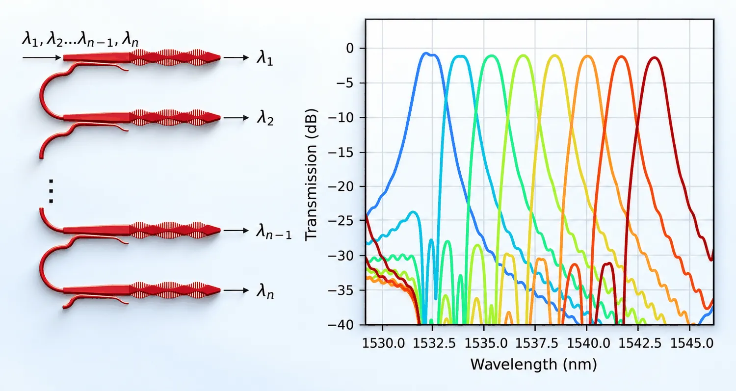
Dense wavelength-division multiplexing (DWDM) carries many channels on one waveguide, spaced a few nanometres apart in the C band. Thin-film lithium niobate (TFLN) is an attractive platform for it, because the same layer that carries the filters also carries high-speed modulators. The filter is the hard part: a shallow-etched TFLN ridge has a weak index contrast, so ring-based filters come out large and thermally sensitive.
This example builds an eight-channel DWDM demultiplexer from multimode waveguide grating (MWG) filters. A corrugation on the sidewalls of a two-mode waveguide reflects the forward TE₀ mode into the backward TE₁ mode. Because the rejected light returns in a different mode, a mode demultiplexer separates it from the incoming light, so the filter needs no circulator and no directional coupler. Three gratings in series enclose two coupled cavities, which turns the broad grating reflection into one narrow flat-top passband. The wavelength of a whole stage is then set by a single number: the length of the phase section between gratings.
The notebook covers:
- the LNOI layer stack and the two-mode waveguide the grating works with,
- the cavity split into gratings and phase sections, so the channels come almost free,
- the linear relation between and channel wavelength, measured with a three-point sweep,
- the mode demultiplexer and the width transitions, each with its own model,
- the eight-stage cascade and its circuit response.
Reference
- Zhu, Mingyu, et al. “Multichannel Lithium-Niobate-On-Insulator Photonic Filter for Dense Wavelength-Division Multiplexing.” ACS Photonics 2025 12 (2), 588-596, doi: 10.1021/acsphotonics.4c00884.
Note on cost: the two grating simulations come to 6.5 FlexCredits together and are reused at every channel, so the channel count does not drive the bill. The mode demultiplexer is the largest single run in the notebook. The three width transitions use eigenmode expansion and are negligible. Every result is cached, so re-running the notebook afterwards is free.
For more integrated photonic examples, please visit our examples page. If you are new to the finite-difference time-domain (FDTD) method, we highly recommend going through our FDTD101 tutorials.
import time
import matplotlib.pyplot as pltimport numpy as npimport photonforge as pfimport tidy3d as tdfrom photonforge.live_viewer import LiveViewer
# Browser-based layout viewer; every component built below is sent to it.viewer = LiveViewer()
LiveViewer started at http://127.0.0.1:45127. Call its 'stop()' method to free the port.The LNOI platform
Section titled “The LNOI platform”The stack is x-cut TFLN: a 400 nm film with a 200 nm partial etch, so a 200 nm slab remains everywhere outside the ridge, air above and buried oxide below. The etch leaves 60 degree sidewalls, measured from the wafer surface, which matters for a corrugated grating and is modelled explicitly rather than as a vertical wall.
Only the media come from Tidy3D. Every geometry, model, and circuit object below is PhotonForge.
lda0 = 1.540                                            # Centre wavelength of the channel comb (um)ldas = np.linspace(1.525, 1.555, 401)                   # Fine grid across the eight channelsfreqs = pf.C_0 / ldaslam = ldas * 1e3                                        # The same grid in nm, for every plot belowfreqs_coarse = pf.C_0 / np.linspace(1.520, 1.560, 21)   # Coarse grid for the smooth components
n_o, n_e = 2.211, 2.138       # Ordinary and extraordinary indices of x-cut LN at 1.55 umn_sio2 = 1.444                # Buried oxide indexh_film, h_slab = 0.400, 0.200                           # Film thickness and remaining slab (um)sidewall_deg = 30.0           # Measured from the wafer normal, so 60 degree sidewallsridge_layer = (1, 0)          # GDS layer of the unetched ridge
The film is birefringent, so it is described with an AnisotropicMedium. Light propagates along and the extraordinary axis lies in the plane of the wafer, transverse to propagation, so the extraordinary index goes on the component.
A PhotonForge Technology bundles the layer stack with
the port specifications, so every component built afterwards inherits the same cross sections and
mode solver settings. Four cross sections are needed: the 1.85 µm multimode waveguide that the
grating is written on, the 2.0 µm end of the mode demultiplexer, its 1.0 µm single-mode input,
and the 0.6 µm routing waveguide. The ridge extrusion carries sidewall_angle referenced to the
top of the film, which puts the slope on every edge including the grating tooth faces.
Each specification takes its modes in order of effective index and applies no polarization filter. On this ridge the ordering already puts TE₀ and TE₁ first, with the nearest TM mode about 0.07 lower in index, so a filter would change nothing. It is worth leaving out: a filtered specification forces the solver to store the full mode field profile at every frequency so that it can re-map mode order, which turns a result of a few hundred kilobytes into several gigabytes.
# Anisotropic LN, with the extraordinary axis transverse to propagation.ln = td.AnisotropicMedium(    xx=td.Medium(permittivity=n_o**2),    yy=td.Medium(permittivity=n_e**2),    zz=td.Medium(permittivity=n_o**2),    name="LN_xcut",)sio2 = td.Medium(permittivity=n_sio2**2, name="SiO2")air = td.Medium(permittivity=1.0, name="air")
# Mode solver window: 1.2 um below the film and 1.6 um above it.port_limits = (-1.2, 1.6)
# One LayerSpec: everything drawn on it stays unetched and becomes the ridge.layers = {"RIDGE": pf.LayerSpec(ridge_layer, "Unetched LN ridge (400 nm)", "#c0002018", "/")}
# Buried oxide, then the slab that survives the partial etch, then the sloped ridge on top.extrusion_specs = [    pf.ExtrusionSpec(pf.MaskSpec(), sio2, (-pf.Z_INF, 0.0)),    pf.ExtrusionSpec(pf.MaskSpec(), ln, (0.0, h_slab)),    pf.ExtrusionSpec(        pf.MaskSpec(ridge_layer), ln, (h_slab, h_film),        sidewall_angle=sidewall_deg, reference="top",    ),]
# The four waveguide cross sections used in the design. Modes are taken in order of effective# index, which on this ridge already puts TE0 and TE1 first, so no polarization filter is needed.ports = {    "MM_1850": pf.PortSpec("Grating waveguide, TE0 and TE1", 5.5, port_limits, num_modes=2,                           target_neff=1.82,                           path_profiles=[(1.850, 0, ridge_layer)], default_radius=100.0),    "MM_2000": pf.PortSpec("Mode demultiplexer wide end, TE0 and TE1", 5.5, port_limits, num_modes=2,                           target_neff=1.82,                           path_profiles=[(2.000, 0, ridge_layer)], default_radius=100.0),    "SM_1000": pf.PortSpec("Mode demultiplexer input, TE0", 4.5, port_limits, num_modes=1,                           target_neff=1.80,                           path_profiles=[(1.000, 0, ridge_layer)], default_radius=100.0),    "SM_600": pf.PortSpec("Single-mode routing waveguide, TE0", 4.0, port_limits, num_modes=1,                          target_neff=1.75,                          path_profiles=[(0.600, 0, ridge_layer)], default_radius=100.0),}
# Make this the default technology so components do not have to name it.tech = pf.Technology("LNOI 400/200 nm, 60 degree sidewalls", "1.0", layers, extrusion_specs, ports, air)pf.config.default_technology = tech
The whole design rests on the 1.85 µm waveguide supporting exactly two TE modes with well separated effective indices, because the grating couples one into the other. Solving the port modes gives those indices and shows the cross section that the sloped sidewall produces.
# Solve the two TE modes of the grating waveguide at the centre wavelength.modes = pf.port_modes("MM_1850", [pf.C_0 / lda0], verbose=False)n_eff = modes.data.n_eff.values.real.ravel()print(f"n_eff at {lda0} um: TE0 = {n_eff[0]:.4f}, TE1 = {n_eff[1]:.4f}")
fig, axs = plt.subplots(1, 3, figsize=(13, 3), tight_layout=True)
# Left panel: the ridge cross section as the mode solver sees it.pf.tidy3d_plot(tech.ports["MM_1850"], ax=axs[0])axs[0].set_title("MM_1850 cross section")
# Right panels: the even TE0 and odd TE1 field profiles the grating couples.for i, ax in enumerate(axs[1:]):    modes.plot_field("Ey", val="abs", mode_index=i, ax=ax, cmap="magma", eps_alpha=0.0)    ax.set_title(f"TE$_{i}$, $n_{{eff}}$ = {n_eff[i]:.4f}")plt.show()
n_eff at 1.54 um: TE0 = 1.8112, TE1 = 1.7281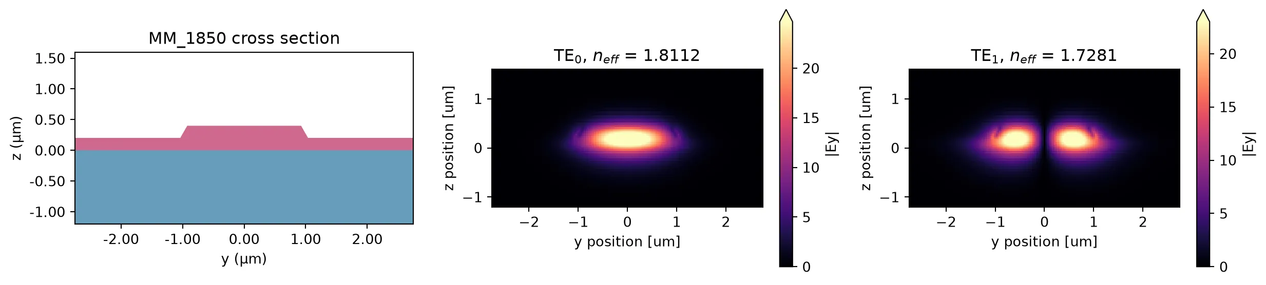
How the filter works
Section titled “How the filter works”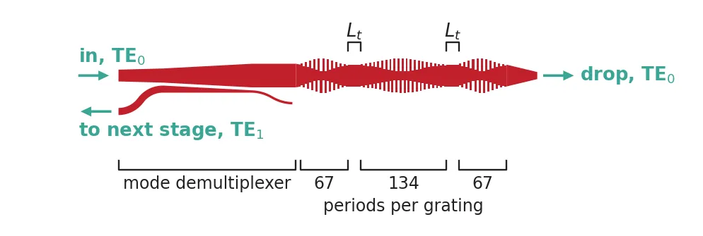
One stage of the demultiplexer, with the phase sections drawn longer than they are so that the three gratings separate visually.
The grating couples forward TE₀ to backward TE₁
Section titled “The grating couples forward TE₀ to backward TE₁”A grating couples two modes when its grating vector makes up the mismatch between their propagation constants. Here one mode travels forward and the other backward, so their propagation constants have opposite signs and the mismatch is their sum:
With the indices solved above this is about 435 nm at 1.54 µm, and the design uses nm.
Phase matching alone is not enough: the perturbation also has to have the right symmetry. TE₀ is even about the waveguide centre line and TE₁ is odd, so a perturbation that is even about that line, such as a uniform width modulation, gives zero overlap between them. The corrugation used here is antisymmetric instead. The waveguide keeps a constant width of 1.85 µm while its centre line steps by for half a period and by for the other half, so the teeth on the two sidewalls are offset by . That perturbation is odd about the centre line, which is exactly what couples an even mode to an odd one.
Why the tooth depth follows three Gaussian humps
Section titled “Why the tooth depth follows three Gaussian humps”A grating that starts and stops abruptly has a rectangular coupling envelope, and its reflection spectrum carries the side lobes that go with it. The corrugation depth here is apodized instead,
so the coupling ramps up and fades away over each grating. The side lobes drop and the stop-band floor sits far below the channel level, which is what keeps crosstalk between neighbouring channels low.
The depth profile of one cavity therefore shows three Gaussian humps, one per grating, not one. The three humps are three mirrors, and their lengths are 67, 134, and 67 periods.
Why three mirrors instead of two
Section titled “Why three mirrors instead of two”A single grating is a mirror: inside its stop band it returns TE₀ as backward TE₁ over a band many nanometres wide, far too broad for a DWDM channel. Two gratings enclose one Fabry-Perot cavity, which transmits a narrow Lorentzian line at each resonance. Three gratings enclose two cavities, coupled to each other through the middle mirror. Two coupled resonances sit side by side, and when their separation is comparable to their linewidth the pair merges into a single passband with a flat top and steeper edges than one resonance can give. The middle grating is twice as long as the outer two, so it is the stronger mirror: the coupling between the two cavities is weaker than the coupling to the outside world, which is the ordering a bandpass filter needs.
How one stage drops a channel and passes the rest
Section titled “How one stage drops a channel and passes the rest”Light enters a stage as TE₀. Two things then happen at once:
- At the cavity resonance, the light tunnels through all three mirrors and leaves the far end of the cavity as forward TE₀. This is the channel that the stage drops.
- Everywhere else in the stop band, the gratings reflect it, and it comes back to the input end as backward TE₁. This is everything the stage does not drop.
The rejected light is in a different mode from the incoming light, so it can be separated by geometry alone. The mode demultiplexer placed in front of the cavity carries forward TE₀ from its single-mode input into the multimode waveguide, and pulls backward TE₁ coming out of the multimode waveguide into a separate narrow waveguide. That narrow waveguide feeds the next stage. Nothing in this path is a circulator or a directional coupler, which is the reason for working in reflection between two modes in the first place.
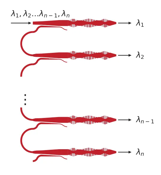
Eight stages in series, each with a slightly different phase-section length , therefore take one channel each out of the comb and pass the remainder along. The hairpin between stages is the route that carries the rejected light from one through port to the next input.
The cavity, one grating at a time
Section titled “The cavity, one grating at a time”The cavity is three gratings separated by two phase sections. Only the phase sections change from channel to channel, so simulating the whole cavity again for every channel repeats the expensive part for nothing. Each grating is instead simulated once on its own, and the cavity is assembled from those results with the phase sections carrying the only thing that differs.
This works because the corrugation is apodized. At the ends of a grating the teeth are about 100 nm deep on a 1850 nm waveguide, so the joints sit in waveguide that is almost unperturbed, where the two guided modes describe the field well.
A grating is built the way the whole cavity would be: the segment list walks along accumulating the length and centre-line offset of each piece, and the two sidewalls are read off that list. A short stub at each end puts the ports on the waveguide centre line, which the last tooth would otherwise leave offset by half a tooth depth.
@pf.parametric_componentdef grating(    *,    n_periods: int = 67,        # Number of corrugation periods    w_mwg: float = 1.850,       # Multimode waveguide width (um)    period: float = 0.4333,     # Corrugation period (um)    delta: float = 1.100,       # Peak corrugation depth (um)    duty: float = 0.5,          # Fraction of the period spent on the upper offset    b_apod: float = 10.0,       # Gaussian apodization strength    pad: float = 0.1,           # On-axis stub at each end, so the ports sit on the centre line) -> pf.Component:    """One Gaussian-apodized multimode waveguide grating."""
    # Gaussian apodization of the tooth depth across the grating.    i = np.arange(1, n_periods + 1)    depths = delta * np.exp(-b_apod * (i - n_periods / 2) ** 2 / n_periods**2)
    # Each period steps the centre line up then down, offsetting the two sidewalls by half a period.    segments = [(pad, 0.0)]    for d in depths:        segments += [(period * duty, 0.5 * d), (period * (1 - duty), -0.5 * d)]    segments.append((pad, 0.0))
    # Turn the segment list into the two sidewalls of a constant-width waveguide.    x, top, bottom = 0.0, [], []    for length, offset in segments:        top += [(x, offset + 0.5 * w_mwg), (x + length, offset + 0.5 * w_mwg)]        bottom += [(x, offset - 0.5 * w_mwg), (x + length, offset - 0.5 * w_mwg)]        x += length
    # Close the outline by running back along the bottom sidewall.    c = pf.Component(f"GRATING_{n_periods}")    c.add("RIDGE", pf.Polygon(top + bottom[::-1]))
    # Find the two waveguide ends from the geometry and name them input first.    p_in, p_out = sorted(c.detect_ports(["MM_1850"], on_boundary="x"), key=lambda p: p.center[0])    c.add_port(p_in, port_name="P0")    c.add_port(p_out, port_name="P1")
    # A lone grating does not resonate, so the default run time is long enough.    c.add_model(pf.Tidy3DModel(verbose=False))    return c
viewer(grating())
Plotting the tooth depths of the three gratings in sequence shows the apodization, and shows the outer gratings at half the length of the middle one.
# Read the shape back from the component, so no number is repeated here.n_periods = (67, 134, 67)shape = grating().parametric_kwargs
# Rebuild the apodized tooth depths of the three gratings.depths = np.concatenate([    shape["delta"] * np.exp(-shape["b_apod"] * (np.arange(1, n + 1) - n / 2) ** 2 / n**2)    for n in n_periods])
fig, ax = plt.subplots(figsize=(7.5, 2.6), tight_layout=True)ax.plot(np.arange(depths.size) * shape["period"], depths * 1e3, color="#c0202a", lw=1.8)ax.set(xlabel="Position along the cavity (um)", ylabel="Tooth depth (nm)")ax.grid(alpha=0.3)plt.show()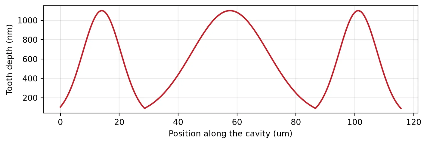
What the decomposition saves
Section titled “What the decomposition saves”The gratings are the only cloud simulations that would otherwise scale with the number of channels. Run once, they serve every channel. These figures were measured on this design.
| FDTD runs | billed | |
|---|---|---|
| One whole cavity, single excitation | 1 | 14.9 FlexCredits |
| Eight channels simulated that way | 8 | about 120 FlexCredits |
| Grating of 67 periods, every excitation | 4 | 1.9 FlexCredits |
| Grating of 134 periods, every excitation | 4 | 4.6 FlexCredits |
| Both gratings, reused at every channel | 8 | 6.5 FlexCredits |
Two effects compound. Each grating is a fraction of the cavity length, and a lone grating does not resonate, so its field decays quickly and the run stops early, while the cavity has to be followed until it rings down. Eight channels therefore cost less than half of one cavity, and every further channel is free.
Each grating needs all four excitations, because the corrugation is not mirror symmetric: a period runs up then down, which reverses when the grating is read from the other end.
# The only cloud simulations in the notebook. Launch both, then collect.gratings = {n: grating(n_periods=n) for n in (67, 134)}runners = {n: g.active_model.start(g, freqs) for n, g in gratings.items()}while any(r.status["message"] == "running" for r in runners.values()):    time.sleep(30)
# Store each result so the cavity reads data instead of calling a solver.for n, g in gratings.items():    g.add_model(pf.DataModel(runners[n].s_matrix, interpolation_method="linear"), "FDTD data")print("gratings simulated:", sorted(gratings))
gratings simulated: [67, 134]Assembling the cavity
Section titled “Assembling the cavity”The cavity is now a circuit: the two simulated gratings, the phase sections between them, and the straight leads at either end. A phase section is a plain two-mode waveguide, and straight already comes with a WaveguideModel, so no model has to be added. With no effective index set, that model solves the cross section and gives each mode the index it actually has, with no mixing between them, which is all a straight waveguide does. The reference_chain function places the pieces end to end, and the numbers in its sequence become these straight sections.
is still the only thing that differs between channels, but changing it now only re-assembles the circuit.
@pf.parametric_componentdef mwg_cavity(    *,    lt: float = 0.434,                 # Phase section between gratings, the channel knob (um)    n_periods: tuple = (67, 134, 67),  # Periods in the three gratings    l_in: float = 1.5,                 # Straight lead into the first grating (um)    l_out: float = 10.5,               # Straight lead out of the last grating (um)    pad: float = 0.1,                  # Stub already carried at each grating end (um)) -> pf.Component:    """Third-order Fabry-Perot cavity, assembled from the simulated gratings."""
    # Lead, then each grating separated by a phase section, then the output lead. The numbers    # in the sequence are the straight sections, with the port specification of the gratings.    gap = f" - {lt - 2 * pad} - "    sequence = f"{l_in - pad} - " + gap.join(f"g{n}" for n in n_periods) + f" - {l_out - pad}"    refs = pf.reference_chain({f"g{n}": gratings[n] for n in n_periods}, sequence)
    # Chain the pieces end to end and expose the two outermost ports.    c = pf.Component(f"MWG_CAVITY_LT{lt * 1e3:.0f}")    c.add(*refs)    c.add_port(refs[0]["P0"], port_name="P0")    c.add_port(refs[-1]["P1"], port_name="P1")
    c.add_model(pf.CircuitModel(verbose=False), "Circuit")    return c
cavity = mwg_cavity()print(f"cavity length: {cavity.size()[0]:.3f} um")viewer(cavity)
cavity length: 128.992 um;fill:%23221f20;font-weight:bold;font-size:0.735968px;}.terminal{fill:none;stroke:%23805080;stroke-width:0.091996;}.dashed{stroke-dasharray:0.459980,0.275988;}.port{fill:none;stroke:%23805080;stroke-width:0.183992;}.virtual-connection{fill:none;stroke:%23907090;stroke-width:0.137994;}.layer_1_0{stroke:%23c00020;fill:url(%23pat-layer_1_0);fill-opacity:0.492;}.label_1_0{fill:%23c00020;}</style><defs><path id=%22port-symbol%22 class=%22port%22 d=%22M 0,-0.367984 L 0.551976,0 0,0.367984%22 /><path id=%22ref-port-symbol%22 class=%22port%22 style=%22stroke-opacity:0.33;%22 d=%22M 0,-0.275988 C 0.367984,-0.275988 0.367984,0.275988 0,0.275988%22 /><circle id=%22port-bend-symbol%22 style=%22stroke-width:0;stroke:none;fill:%23805080;fill-opacity:1;%22 cx=%220%22 cy=%220%22 r=%220.165593%22 /><circle id=%22connection-symbol%22 style=%22stroke-width:0;stroke:none;fill:%23907090;fill-opacity:1;%22 cx=%220%22 cy=%220%22 r=%220.193192%22 /><pattern id=%22pat-layer_1_0%22 patternUnits=%22userSpaceOnUse%22 width=%220.459980%22 height=%220.459980%22 patternTransform=%22translate(0.189404,0.266304)%22><line x1=%220%22 y1=%220%22 x2=%220.459980%22 y2=%220.459980%22 style=%22stroke:%23c00020;stroke-width:0.045998%22 /><line x1=%22-0.229990%22 y1=%220.229990%22 x2=%220.229990%22 y2=%220.689970%22 style=%22stroke:%23c00020;stroke-width:0.045998%22 /><line x1=%220.229990%22 y1=%22-0.229990%22 x2=%220.689970%22 y2=%220.229990%22 style=%22stroke:%23c00020;stroke-width:0.045998%22 /></pattern><g id=%22C1%22 data-name=%22straight__HZELSZ7Y6PQG3I45LHLPVZQLT3BZEGPLWJAWJROFJKRP6B2ZENMA%22><path class=%22layer_1_0%22 d=%22M 0.000000,-0.925000 1.400000,-0.925000 1.400000,0.925000 0.000000,0.925000 z%22 /></g><g id=%22C2%22 data-name=%22GRATING_67%22><path class=%22layer_1_0%22 d=%22M 0.000000,-0.925000 0.100000,-0.925000 0.100000,-0.873000 0.317000,-0.873000 0.317000,-0.977000 0.533000,-0.977000 0.533000,-0.865000 0.750000,-0.865000 0.750000,-0.985000 0.967000,-0.985000 0.967000,-0.856000 1.183000,-0.856000 1.183000,-0.994000 1.400000,-0.994000 1.400000,-0.846000 1.617000,-0.846000 1.617000,-1.004000 1.833000,-1.004000 1.833000,-0.835000 2.050000,-0.835000 2.050000,-1.015000 2.267000,-1.015000 2.267000,-0.823000 2.483000,-0.823000 2.483000,-1.027000 2.700000,-1.027000 2.700000,-0.810000 2.916000,-0.810000 2.916000,-1.040000 3.133000,-1.040000 3.133000,-0.796000 3.350000,-0.796000 3.350000,-1.054000 3.566000,-1.054000 3.566000,-0.781000 3.783000,-0.781000 3.783000,-1.069000 4.000000,-1.069000 4.000000,-0.764000 4.216000,-0.764000 4.216000,-1.086000 4.433000,-1.086000 4.433000,-0.747000 4.650000,-0.747000 4.650000,-1.103000 4.866000,-1.103000 4.866000,-0.729000 5.083000,-0.729000 5.083000,-1.121000 5.300000,-1.121000 5.300000,-0.709000 5.516000,-0.709000 5.516000,-1.141000 5.733000,-1.141000 5.733000,-0.689000 5.950000,-0.689000 5.950000,-1.161000 6.166000,-1.161000 6.166000,-0.668000 6.383000,-0.668000 6.383000,-1.182000 6.600000,-1.182000 6.600000,-0.647000 6.816000,-0.647000 6.816000,-1.203000 7.033000,-1.203000 7.033000,-0.625000 7.249000,-0.625000 7.249000,-1.225000 7.466000,-1.225000 7.466000,-0.603000 7.683000,-0.603000 7.683000,-1.247000 7.899000,-1.247000 7.899000,-0.581000 8.116000,-0.581000 8.116000,-1.269000 8.333000,-1.269000 8.333000,-0.559000 8.549000,-0.559000 8.549000,-1.291000 8.766000,-1.291000 8.766000,-0.537000 8.983000,-0.537000 8.983000,-1.313000 9.199000,-1.313000 9.199000,-0.515000 9.416000,-0.515000 9.416000,-1.335000 9.633000,-1.335000 9.633000,-0.495000 9.849000,-0.495000 9.849000,-1.355000 10.066000,-1.355000 10.066000,-0.475000 10.283000,-0.475000 10.283000,-1.375000 10.499000,-1.375000 10.499000,-0.457000 10.716000,-0.457000 10.716000,-1.393000 10.933000,-1.393000 10.933000,-0.440000 11.149000,-0.440000 11.149000,-1.410000 11.366000,-1.410000 11.366000,-0.424000 11.582000,-0.424000 11.582000,-1.426000 11.799000,-1.426000 11.799000,-0.411000 12.016000,-0.411000 12.016000,-1.439000 12.232000,-1.439000 12.232000,-0.399000 12.449000,-0.399000 12.449000,-1.451000 12.666000,-1.451000 12.666000,-0.390000 12.882000,-0.390000 12.882000,-1.460000 13.099000,-1.460000 13.099000,-0.383000 13.316000,-0.383000 13.316000,-1.467000 13.532000,-1.467000 13.532000,-0.378000 13.749000,-0.378000 13.749000,-1.472000 13.966000,-1.472000 13.966000,-0.375000 14.182000,-0.375000 14.182000,-1.475000 14.399000,-1.475000 14.399000,-0.375000 14.616000,-0.375000 14.616000,-1.475000 14.832000,-1.475000 14.832000,-0.378000 15.049000,-0.378000 15.049000,-1.472000 15.266000,-1.472000 15.266000,-0.383000 15.482000,-0.383000 15.482000,-1.467000 15.699000,-1.467000 15.699000,-0.390000 15.915000,-0.390000 15.915000,-1.460000 16.132000,-1.460000 16.132000,-0.399000 16.349000,-0.399000 16.349000,-1.451000 16.565000,-1.451000 16.565000,-0.411000 16.782000,-0.411000 16.782000,-1.439000 16.999000,-1.439000 16.999000,-0.424000 17.215000,-0.424000 17.215000,-1.426000 17.432000,-1.426000 17.432000,-0.440000 17.649000,-0.440000 17.649000,-1.410000 17.865000,-1.410000 17.865000,-0.457000 18.082000,-0.457000 18.082000,-1.393000 18.299000,-1.393000 18.299000,-0.475000 18.515000,-0.475000 18.515000,-1.375000 18.732000,-1.375000 18.732000,-0.495000 18.949000,-0.495000 18.949000,-1.355000 19.165000,-1.355000 19.165000,-0.515000 19.382000,-0.515000 19.382000,-1.335000 19.599000,-1.335000 19.599000,-0.537000 19.815000,-0.537000 19.815000,-1.313000 20.032000,-1.313000 20.032000,-0.559000 20.248000,-0.559000 20.248000,-1.291000 20.465000,-1.291000 20.465000,-0.581000 20.682000,-0.581000 20.682000,-1.269000 20.898000,-1.269000 20.898000,-0.603000 21.115000,-0.603000 21.115000,-1.247000 21.332000,-1.247000 21.332000,-0.625000 21.548000,-0.625000 21.548000,-1.225000 21.765000,-1.225000 21.765000,-0.647000 21.982000,-0.647000 21.982000,-1.203000 22.198000,-1.203000 22.198000,-0.668000 22.415000,-0.668000 22.415000,-1.182000 22.632000,-1.182000 22.632000,-0.689000 22.848000,-0.689000 22.848000,-1.161000 23.065000,-1.161000 23.065000,-0.709000 23.282000,-0.709000 23.282000,-1.141000 23.498000,-1.141000 23.498000,-0.729000 23.715000,-0.729000 23.715000,-1.121000 23.932000,-1.121000 23.932000,-0.747000 24.148000,-0.747000 24.148000,-1.103000 24.365000,-1.103000 24.365000,-0.764000 24.581000,-0.764000 24.581000,-1.086000 24.798000,-1.086000 24.798000,-0.781000 25.015000,-0.781000 25.015000,-1.069000 25.231000,-1.069000 25.231000,-0.796000 25.448000,-0.796000 25.448000,-1.054000 25.665000,-1.054000 25.665000,-0.810000 25.881000,-0.810000 25.881000,-1.040000 26.098000,-1.040000 26.098000,-0.823000 26.315000,-0.823000 26.315000,-1.027000 26.531000,-1.027000 26.531000,-0.835000 26.748000,-0.835000 26.748000,-1.015000 26.965000,-1.015000 26.965000,-0.846000 27.181000,-0.846000 27.181000,-1.004000 27.398000,-1.004000 27.398000,-0.856000 27.615000,-0.856000 27.615000,-0.994000 27.831000,-0.994000 27.831000,-0.865000 28.048000,-0.865000 28.048000,-0.985000 28.265000,-0.985000 28.265000,-0.873000 28.481000,-0.873000 28.481000,-0.977000 28.698000,-0.977000 28.698000,-0.880000 28.914000,-0.880000 28.914000,-0.970000 29.131000,-0.970000 29.131000,-0.925000 29.231000,-0.925000 29.231000,0.925000 29.131000,0.925000 29.131000,0.880000 28.914000,0.880000 28.914000,0.970000 28.698000,0.970000 28.698000,0.873000 28.481000,0.873000 28.481000,0.977000 28.265000,0.977000 28.265000,0.865000 28.048000,0.865000 28.048000,0.985000 27.831000,0.985000 27.831000,0.856000 27.615000,0.856000 27.615000,0.994000 27.398000,0.994000 27.398000,0.846000 27.181000,0.846000 27.181000,1.004000 26.965000,1.004000 26.965000,0.835000 26.748000,0.835000 26.748000,1.015000 26.531000,1.015000 26.531000,0.823000 26.315000,0.823000 26.315000,1.027000 26.098000,1.027000 26.098000,0.810000 25.881000,0.810000 25.881000,1.040000 25.665000,1.040000 25.665000,0.796000 25.448000,0.796000 25.448000,1.054000 25.231000,1.054000 25.231000,0.781000 25.015000,0.781000 25.015000,1.069000 24.798000,1.069000 24.798000,0.764000 24.581000,0.764000 24.581000,1.086000 24.365000,1.086000 24.365000,0.747000 24.148000,0.747000 24.148000,1.103000 23.932000,1.103000 23.932000,0.729000 23.715000,0.729000 23.715000,1.121000 23.498000,1.121000 23.498000,0.709000 23.282000,0.709000 23.282000,1.141000 23.065000,1.141000 23.065000,0.689000 22.848000,0.689000 22.848000,1.161000 22.632000,1.161000 22.632000,0.668000 22.415000,0.668000 22.415000,1.182000 22.198000,1.182000 22.198000,0.647000 21.982000,0.647000 21.982000,1.203000 21.765000,1.203000 21.765000,0.625000 21.548000,0.625000 21.548000,1.225000 21.332000,1.225000 21.332000,0.603000 21.115000,0.603000 21.115000,1.247000 20.898000,1.247000 20.898000,0.581000 20.682000,0.581000 20.682000,1.269000 20.465000,1.269000 20.465000,0.559000 20.248000,0.559000 20.248000,1.291000 20.032000,1.291000 20.032000,0.537000 19.815000,0.537000 19.815000,1.313000 19.599000,1.313000 19.599000,0.515000 19.382000,0.515000 19.382000,1.335000 19.165000,1.335000 19.165000,0.495000 18.949000,0.495000 18.949000,1.355000 18.732000,1.355000 18.732000,0.475000 18.515000,0.475000 18.515000,1.375000 18.299000,1.375000 18.299000,0.457000 18.082000,0.457000 18.082000,1.393000 17.865000,1.393000 17.865000,0.440000 17.649000,0.440000 17.649000,1.410000 17.432000,1.410000 17.432000,0.424000 17.215000,0.424000 17.215000,1.426000 16.999000,1.426000 16.999000,0.411000 16.782000,0.411000 16.782000,1.439000 16.565000,1.439000 16.565000,0.399000 16.349000,0.399000 16.349000,1.451000 16.132000,1.451000 16.132000,0.390000 15.915000,0.390000 15.915000,1.460000 15.699000,1.460000 15.699000,0.383000 15.482000,0.383000 15.482000,1.467000 15.266000,1.467000 15.266000,0.378000 15.049000,0.378000 15.049000,1.472000 14.832000,1.472000 14.832000,0.375000 14.616000,0.375000 14.616000,1.475000 14.399000,1.475000 14.399000,0.375000 14.182000,0.375000 14.182000,1.475000 13.966000,1.475000 13.966000,0.378000 13.749000,0.378000 13.749000,1.472000 13.532000,1.472000 13.532000,0.383000 13.316000,0.383000 13.316000,1.467000 13.099000,1.467000 13.099000,0.390000 12.882000,0.390000 12.882000,1.460000 12.666000,1.460000 12.666000,0.399000 12.449000,0.399000 12.449000,1.451000 12.232000,1.451000 12.232000,0.411000 12.016000,0.411000 12.016000,1.439000 11.799000,1.439000 11.799000,0.424000 11.582000,0.424000 11.582000,1.426000 11.366000,1.426000 11.366000,0.440000 11.149000,0.440000 11.149000,1.410000 10.933000,1.410000 10.933000,0.457000 10.716000,0.457000 10.716000,1.393000 10.499000,1.393000 10.499000,0.475000 10.283000,0.475000 10.283000,1.375000 10.066000,1.375000 10.066000,0.495000 9.849000,0.495000 9.849000,1.355000 9.633000,1.355000 9.633000,0.515000 9.416000,0.515000 9.416000,1.335000 9.199000,1.335000 9.199000,0.537000 8.983000,0.537000 8.983000,1.313000 8.766000,1.313000 8.766000,0.559000 8.549000,0.559000 8.549000,1.291000 8.333000,1.291000 8.333000,0.581000 8.116000,0.581000 8.116000,1.269000 7.899000,1.269000 7.899000,0.603000 7.683000,0.603000 7.683000,1.247000 7.466000,1.247000 7.466000,0.625000 7.249000,0.625000 7.249000,1.225000 7.033000,1.225000 7.033000,0.647000 6.816000,0.647000 6.816000,1.203000 6.600000,1.203000 6.600000,0.668000 6.383000,0.668000 6.383000,1.182000 6.166000,1.182000 6.166000,0.689000 5.950000,0.689000 5.950000,1.161000 5.733000,1.161000 5.733000,0.709000 5.516000,0.709000 5.516000,1.141000 5.300000,1.141000 5.300000,0.729000 5.083000,0.729000 5.083000,1.121000 4.866000,1.121000 4.866000,0.747000 4.650000,0.747000 4.650000,1.103000 4.433000,1.103000 4.433000,0.764000 4.216000,0.764000 4.216000,1.086000 4.000000,1.086000 4.000000,0.781000 3.783000,0.781000 3.783000,1.069000 3.566000,1.069000 3.566000,0.796000 3.350000,0.796000 3.350000,1.054000 3.133000,1.054000 3.133000,0.810000 2.916000,0.810000 2.916000,1.040000 2.700000,1.040000 2.700000,0.823000 2.483000,0.823000 2.483000,1.027000 2.267000,1.027000 2.267000,0.835000 2.050000,0.835000 2.050000,1.015000 1.833000,1.015000 1.833000,0.846000 1.617000,0.846000 1.617000,1.004000 1.400000,1.004000 1.400000,0.856000 1.183000,0.856000 1.183000,0.994000 0.967000,0.994000 0.967000,0.865000 0.750000,0.865000 0.750000,0.985000 0.533000,0.985000 0.533000,0.873000 0.317000,0.873000 0.317000,0.977000 0.100000,0.977000 0.100000,0.925000 0.000000,0.925000 z%22 /></g><g id=%22C3%22 data-name=%22straight__3DIPTEFGIVEVI53Y6BKQACHWGANGXTONM6ONWOTYXHU7IU2R5JPA%22><path class=%22layer_1_0%22 d=%22M 0.000000,-0.925000 0.234000,-0.925000 0.234000,0.925000 0.000000,0.925000 z%22 /></g><g id=%22C4%22 data-name=%22GRATING_134%22><path class=%22layer_1_0%22 d=%22M 0.000000,-0.925000 0.100000,-0.925000 0.100000,-0.876000 0.317000,-0.876000 0.317000,-0.974000 0.533000,-0.974000 0.533000,-0.873000 0.750000,-0.873000 0.750000,-0.977000 0.967000,-0.977000 0.967000,-0.869000 1.183000,-0.869000 1.183000,-0.981000 1.400000,-0.981000 1.400000,-0.865000 1.617000,-0.865000 1.617000,-0.985000 1.833000,-0.985000 1.833000,-0.860000 2.050000,-0.860000 2.050000,-0.990000 2.267000,-0.990000 2.267000,-0.856000 2.483000,-0.856000 2.483000,-0.994000 2.700000,-0.994000 2.700000,-0.851000 2.916000,-0.851000 2.916000,-0.999000 3.133000,-0.999000 3.133000,-0.846000 3.350000,-0.846000 3.350000,-1.004000 3.566000,-1.004000 3.566000,-0.841000 3.783000,-0.841000 3.783000,-1.009000 4.000000,-1.009000 4.000000,-0.835000 4.216000,-0.835000 4.216000,-1.015000 4.433000,-1.015000 4.433000,-0.829000 4.650000,-0.829000 4.650000,-1.021000 4.866000,-1.021000 4.866000,-0.823000 5.083000,-0.823000 5.083000,-1.027000 5.300000,-1.027000 5.300000,-0.817000 5.516000,-0.817000 5.516000,-1.033000 5.733000,-1.033000 5.733000,-0.810000 5.950000,-0.810000 5.950000,-1.040000 6.166000,-1.040000 6.166000,-0.803000 6.383000,-0.803000 6.383000,-1.047000 6.600000,-1.047000 6.600000,-0.796000 6.816000,-0.796000 6.816000,-1.054000 7.033000,-1.054000 7.033000,-0.788000 7.249000,-0.788000 7.249000,-1.062000 7.466000,-1.062000 7.466000,-0.781000 7.683000,-0.781000 7.683000,-1.069000 7.899000,-1.069000 7.899000,-0.773000 8.116000,-0.773000 8.116000,-1.077000 8.333000,-1.077000 8.333000,-0.764000 8.549000,-0.764000 8.549000,-1.086000 8.766000,-1.086000 8.766000,-0.756000 8.983000,-0.756000 8.983000,-1.094000 9.199000,-1.094000 9.199000,-0.747000 9.416000,-0.747000 9.416000,-1.103000 9.633000,-1.103000 9.633000,-0.738000 9.849000,-0.738000 9.849000,-1.112000 10.066000,-1.112000 10.066000,-0.729000 10.283000,-0.729000 10.283000,-1.121000 10.499000,-1.121000 10.499000,-0.719000 10.716000,-0.719000 10.716000,-1.131000 10.933000,-1.131000 10.933000,-0.709000 11.149000,-0.709000 11.149000,-1.141000 11.366000,-1.141000 11.366000,-0.699000 11.582000,-0.699000 11.582000,-1.151000 11.799000,-1.151000 11.799000,-0.689000 12.016000,-0.689000 12.016000,-1.161000 12.232000,-1.161000 12.232000,-0.679000 12.449000,-0.679000 12.449000,-1.171000 12.666000,-1.171000 12.666000,-0.668000 12.882000,-0.668000 12.882000,-1.182000 13.099000,-1.182000 13.099000,-0.658000 13.316000,-0.658000 13.316000,-1.192000 13.532000,-1.192000 13.532000,-0.647000 13.749000,-0.647000 13.749000,-1.203000 13.966000,-1.203000 13.966000,-0.636000 14.182000,-0.636000 14.182000,-1.214000 14.399000,-1.214000 14.399000,-0.625000 14.616000,-0.625000 14.616000,-1.225000 14.832000,-1.225000 14.832000,-0.614000 15.049000,-0.614000 15.049000,-1.236000 15.266000,-1.236000 15.266000,-0.603000 15.482000,-0.603000 15.482000,-1.247000 15.699000,-1.247000 15.699000,-0.592000 15.915000,-0.592000 15.915000,-1.258000 16.132000,-1.258000 16.132000,-0.581000 16.349000,-0.581000 16.349000,-1.269000 16.565000,-1.269000 16.565000,-0.570000 16.782000,-0.570000 16.782000,-1.280000 16.999000,-1.280000 16.999000,-0.559000 17.215000,-0.559000 17.215000,-1.291000 17.432000,-1.291000 17.432000,-0.548000 17.649000,-0.548000 17.649000,-1.302000 17.865000,-1.302000 17.865000,-0.537000 18.082000,-0.537000 18.082000,-1.313000 18.299000,-1.313000 18.299000,-0.526000 18.515000,-0.526000 18.515000,-1.324000 18.732000,-1.324000 18.732000,-0.515000 18.949000,-0.515000 18.949000,-1.335000 19.165000,-1.335000 19.165000,-0.505000 19.382000,-0.505000 19.382000,-1.345000 19.599000,-1.345000 19.599000,-0.495000 19.815000,-0.495000 19.815000,-1.355000 20.032000,-1.355000 20.032000,-0.485000 20.248000,-0.485000 20.248000,-1.365000 20.465000,-1.365000 20.465000,-0.475000 20.682000,-0.475000 20.682000,-1.375000 20.898000,-1.375000 20.898000,-0.466000 21.115000,-0.466000 21.115000,-1.384000 21.332000,-1.384000 21.332000,-0.457000 21.548000,-0.457000 21.548000,-1.393000 21.765000,-1.393000 21.765000,-0.448000 21.982000,-0.448000 21.982000,-1.402000 22.198000,-1.402000 22.198000,-0.440000 22.415000,-0.440000 22.415000,-1.410000 22.632000,-1.410000 22.632000,-0.432000 22.848000,-0.432000 22.848000,-1.418000 23.065000,-1.418000 23.065000,-0.424000 23.282000,-0.424000 23.282000,-1.426000 23.498000,-1.426000 23.498000,-0.417000 23.715000,-0.417000 23.715000,-1.433000 23.932000,-1.433000 23.932000,-0.411000 24.148000,-0.411000 24.148000,-1.439000 24.365000,-1.439000 24.365000,-0.405000 24.581000,-0.405000 24.581000,-1.445000 24.798000,-1.445000 24.798000,-0.399000 25.015000,-0.399000 25.015000,-1.451000 25.231000,-1.451000 25.231000,-0.394000 25.448000,-0.394000 25.448000,-1.456000 25.665000,-1.456000 25.665000,-0.390000 25.881000,-0.390000 25.881000,-1.460000 26.098000,-1.460000 26.098000,-0.386000 26.315000,-0.386000 26.315000,-1.464000 26.531000,-1.464000 26.531000,-0.383000 26.748000,-0.383000 26.748000,-1.467000 26.965000,-1.467000 26.965000,-0.380000 27.181000,-0.380000 27.181000,-1.470000 27.398000,-1.470000 27.398000,-0.378000 27.615000,-0.378000 27.615000,-1.472000 27.831000,-1.472000 27.831000,-0.376000 28.048000,-0.376000 28.048000,-1.474000 28.265000,-1.474000 28.265000,-0.375000 28.481000,-0.375000 28.481000,-1.475000 28.698000,-1.475000 28.698000,-0.375000 28.914000,-0.375000 28.914000,-1.475000 29.131000,-1.475000 29.131000,-0.375000 29.348000,-0.375000 29.348000,-1.475000 29.564000,-1.475000 29.564000,-0.376000 29.781000,-0.376000 29.781000,-1.474000 29.998000,-1.474000 29.998000,-0.378000 30.214000,-0.378000 30.214000,-1.472000 30.431000,-1.472000 30.431000,-0.380000 30.648000,-0.380000 30.648000,-1.470000 30.864000,-1.470000 30.864000,-0.383000 31.081000,-0.383000 31.081000,-1.467000 31.298000,-1.467000 31.298000,-0.386000 31.514000,-0.386000 31.514000,-1.464000 31.731000,-1.464000 31.731000,-0.390000 31.948000,-0.390000 31.948000,-1.460000 32.164000,-1.460000 32.164000,-0.394000 32.381000,-0.394000 32.381000,-1.456000 32.598000,-1.456000 32.598000,-0.399000 32.814000,-0.399000 32.814000,-1.451000 33.031000,-1.451000 33.031000,-0.405000 33.247000,-0.405000 33.247000,-1.445000 33.464000,-1.445000 33.464000,-0.411000 33.681000,-0.411000 33.681000,-1.439000 33.897000,-1.439000 33.897000,-0.417000 34.114000,-0.417000 34.114000,-1.433000 34.331000,-1.433000 34.331000,-0.424000 34.547000,-0.424000 34.547000,-1.426000 34.764000,-1.426000 34.764000,-0.432000 34.981000,-0.432000 34.981000,-1.418000 35.197000,-1.418000 35.197000,-0.440000 35.414000,-0.440000 35.414000,-1.410000 35.631000,-1.410000 35.631000,-0.448000 35.847000,-0.448000 35.847000,-1.402000 36.064000,-1.402000 36.064000,-0.457000 36.281000,-0.457000 36.281000,-1.393000 36.497000,-1.393000 36.497000,-0.466000 36.714000,-0.466000 36.714000,-1.384000 36.931000,-1.384000 36.931000,-0.475000 37.147000,-0.475000 37.147000,-1.375000 37.364000,-1.375000 37.364000,-0.485000 37.580000,-0.485000 37.580000,-1.365000 37.797000,-1.365000 37.797000,-0.495000 38.014000,-0.495000 38.014000,-1.355000 38.230000,-1.355000 38.230000,-0.505000 38.447000,-0.505000 38.447000,-1.345000 38.664000,-1.345000 38.664000,-0.515000 38.880000,-0.515000 38.880000,-1.335000 39.097000,-1.335000 39.097000,-0.526000 39.314000,-0.526000 39.314000,-1.324000 39.530000,-1.324000 39.530000,-0.537000 39.747000,-0.537000 39.747000,-1.313000 39.964000,-1.313000 39.964000,-0.548000 40.180000,-0.548000 40.180000,-1.302000 40.397000,-1.302000 40.397000,-0.559000 40.614000,-0.559000 40.614000,-1.291000 40.830000,-1.291000 40.830000,-0.570000 41.047000,-0.570000 41.047000,-1.280000 41.264000,-1.280000 41.264000,-0.581000 41.480000,-0.581000 41.480000,-1.269000 41.697000,-1.269000 41.697000,-0.592000 41.913000,-0.592000 41.913000,-1.258000 42.130000,-1.258000 42.130000,-0.603000 42.347000,-0.603000 42.347000,-1.247000 42.563000,-1.247000 42.563000,-0.614000 42.780000,-0.614000 42.780000,-1.236000 42.997000,-1.236000 42.997000,-0.625000 43.213000,-0.625000 43.213000,-1.225000 43.430000,-1.225000 43.430000,-0.636000 43.647000,-0.636000 43.647000,-1.214000 43.863000,-1.214000 43.863000,-0.647000 44.080000,-0.647000 44.080000,-1.203000 44.297000,-1.203000 44.297000,-0.658000 44.513000,-0.658000 44.513000,-1.192000 44.730000,-1.192000 44.730000,-0.668000 44.947000,-0.668000 44.947000,-1.182000 45.163000,-1.182000 45.163000,-0.679000 45.380000,-0.679000 45.380000,-1.171000 45.597000,-1.171000 45.597000,-0.689000 45.813000,-0.689000 45.813000,-1.161000 46.030000,-1.161000 46.030000,-0.699000 46.246000,-0.699000 46.246000,-1.151000 46.463000,-1.151000 46.463000,-0.709000 46.680000,-0.709000 46.680000,-1.141000 46.896000,-1.141000 46.896000,-0.719000 47.113000,-0.719000 47.113000,-1.131000 47.330000,-1.131000 47.330000,-0.729000 47.546000,-0.729000 47.546000,-1.121000 47.763000,-1.121000 47.763000,-0.738000 47.980000,-0.738000 47.980000,-1.112000 48.196000,-1.112000 48.196000,-0.747000 48.413000,-0.747000 48.413000,-1.103000 48.630000,-1.103000 48.630000,-0.756000 48.846000,-0.756000 48.846000,-1.094000 49.063000,-1.094000 49.063000,-0.764000 49.280000,-0.764000 49.280000,-1.086000 49.496000,-1.086000 49.496000,-0.773000 49.713000,-0.773000 49.713000,-1.077000 49.930000,-1.077000 49.930000,-0.781000 50.146000,-0.781000 50.146000,-1.069000 50.363000,-1.069000 50.363000,-0.788000 50.579000,-0.788000 50.579000,-1.062000 50.796000,-1.062000 50.796000,-0.796000 51.013000,-0.796000 51.013000,-1.054000 51.229000,-1.054000 51.229000,-0.803000 51.446000,-0.803000 51.446000,-1.047000 51.663000,-1.047000 51.663000,-0.810000 51.879000,-0.810000 51.879000,-1.040000 52.096000,-1.040000 52.096000,-0.817000 52.313000,-0.817000 52.313000,-1.033000 52.529000,-1.033000 52.529000,-0.823000 52.746000,-0.823000 52.746000,-1.027000 52.963000,-1.027000 52.963000,-0.829000 53.179000,-0.829000 53.179000,-1.021000 53.396000,-1.021000 53.396000,-0.835000 53.613000,-0.835000 53.613000,-1.015000 53.829000,-1.015000 53.829000,-0.841000 54.046000,-0.841000 54.046000,-1.009000 54.263000,-1.009000 54.263000,-0.846000 54.479000,-0.846000 54.479000,-1.004000 54.696000,-1.004000 54.696000,-0.851000 54.912000,-0.851000 54.912000,-0.999000 55.129000,-0.999000 55.129000,-0.856000 55.346000,-0.856000 55.346000,-0.994000 55.562000,-0.994000 55.562000,-0.860000 55.779000,-0.860000 55.779000,-0.990000 55.996000,-0.990000 55.996000,-0.865000 56.212000,-0.865000 56.212000,-0.985000 56.429000,-0.985000 56.429000,-0.869000 56.646000,-0.869000 56.646000,-0.981000 56.862000,-0.981000 56.862000,-0.873000 57.079000,-0.873000 57.079000,-0.977000 57.296000,-0.977000 57.296000,-0.876000 57.512000,-0.876000 57.512000,-0.974000 57.729000,-0.974000 57.729000,-0.880000 57.946000,-0.880000 57.946000,-0.970000 58.162000,-0.970000 58.162000,-0.925000 58.262000,-0.925000 58.262000,0.925000 58.162000,0.925000 58.162000,0.880000 57.946000,0.880000 57.946000,0.970000 57.729000,0.970000 57.729000,0.876000 57.512000,0.876000 57.512000,0.974000 57.296000,0.974000 57.296000,0.873000 57.079000,0.873000 57.079000,0.977000 56.862000,0.977000 56.862000,0.869000 56.646000,0.869000 56.646000,0.981000 56.429000,0.981000 56.429000,0.865000 56.212000,0.865000 56.212000,0.985000 55.996000,0.985000 55.996000,0.860000 55.779000,0.860000 55.779000,0.990000 55.562000,0.990000 55.562000,0.856000 55.346000,0.856000 55.346000,0.994000 55.129000,0.994000 55.129000,0.851000 54.912000,0.851000 54.912000,0.999000 54.696000,0.999000 54.696000,0.846000 54.479000,0.846000 54.479000,1.004000 54.263000,1.004000 54.263000,0.841000 54.046000,0.841000 54.046000,1.009000 53.829000,1.009000 53.829000,0.835000 53.613000,0.835000 53.613000,1.015000 53.396000,1.015000 53.396000,0.829000 53.179000,0.829000 53.179000,1.021000 52.963000,1.021000 52.963000,0.823000 52.746000,0.823000 52.746000,1.027000 52.529000,1.027000 52.529000,0.817000 52.313000,0.817000 52.313000,1.033000 52.096000,1.033000 52.096000,0.810000 51.879000,0.810000 51.879000,1.040000 51.663000,1.040000 51.663000,0.803000 51.446000,0.803000 51.446000,1.047000 51.229000,1.047000 51.229000,0.796000 51.013000,0.796000 51.013000,1.054000 50.796000,1.054000 50.796000,0.788000 50.579000,0.788000 50.579000,1.062000 50.363000,1.062000 50.363000,0.781000 50.146000,0.781000 50.146000,1.069000 49.930000,1.069000 49.930000,0.773000 49.713000,0.773000 49.713000,1.077000 49.496000,1.077000 49.496000,0.764000 49.280000,0.764000 49.280000,1.086000 49.063000,1.086000 49.063000,0.756000 48.846000,0.756000 48.846000,1.094000 48.630000,1.094000 48.630000,0.747000 48.413000,0.747000 48.413000,1.103000 48.196000,1.103000 48.196000,0.738000 47.980000,0.738000 47.980000,1.112000 47.763000,1.112000 47.763000,0.729000 47.546000,0.729000 47.546000,1.121000 47.330000,1.121000 47.330000,0.719000 47.113000,0.719000 47.113000,1.131000 46.896000,1.131000 46.896000,0.709000 46.680000,0.709000 46.680000,1.141000 46.463000,1.141000 46.463000,0.699000 46.246000,0.699000 46.246000,1.151000 46.030000,1.151000 46.030000,0.689000 45.813000,0.689000 45.813000,1.161000 45.597000,1.161000 45.597000,0.679000 45.380000,0.679000 45.380000,1.171000 45.163000,1.171000 45.163000,0.668000 44.947000,0.668000 44.947000,1.182000 44.730000,1.182000 44.730000,0.658000 44.513000,0.658000 44.513000,1.192000 44.297000,1.192000 44.297000,0.647000 44.080000,0.647000 44.080000,1.203000 43.863000,1.203000 43.863000,0.636000 43.647000,0.636000 43.647000,1.214000 43.430000,1.214000 43.430000,0.625000 43.213000,0.625000 43.213000,1.225000 42.997000,1.225000 42.997000,0.614000 42.780000,0.614000 42.780000,1.236000 42.563000,1.236000 42.563000,0.603000 42.347000,0.603000 42.347000,1.247000 42.130000,1.247000 42.130000,0.592000 41.913000,0.592000 41.913000,1.258000 41.697000,1.258000 41.697000,0.581000 41.480000,0.581000 41.480000,1.269000 41.264000,1.269000 41.264000,0.570000 41.047000,0.570000 41.047000,1.280000 40.830000,1.280000 40.830000,0.559000 40.614000,0.559000 40.614000,1.291000 40.397000,1.291000 40.397000,0.548000 40.180000,0.548000 40.180000,1.302000 39.964000,1.302000 39.964000,0.537000 39.747000,0.537000 39.747000,1.313000 39.530000,1.313000 39.530000,0.526000 39.314000,0.526000 39.314000,1.324000 39.097000,1.324000 39.097000,0.515000 38.880000,0.515000 38.880000,1.335000 38.664000,1.335000 38.664000,0.505000 38.447000,0.505000 38.447000,1.345000 38.230000,1.345000 38.230000,0.495000 38.014000,0.495000 38.014000,1.355000 37.797000,1.355000 37.797000,0.485000 37.580000,0.485000 37.580000,1.365000 37.364000,1.365000 37.364000,0.475000 37.147000,0.475000 37.147000,1.375000 36.931000,1.375000 36.931000,0.466000 36.714000,0.466000 36.714000,1.384000 36.497000,1.384000 36.497000,0.457000 36.281000,0.457000 36.281000,1.393000 36.064000,1.393000 36.064000,0.448000 35.847000,0.448000 35.847000,1.402000 35.631000,1.402000 35.631000,0.440000 35.414000,0.440000 35.414000,1.410000 35.197000,1.410000 35.197000,0.432000 34.981000,0.432000 34.981000,1.418000 34.764000,1.418000 34.764000,0.424000 34.547000,0.424000 34.547000,1.426000 34.331000,1.426000 34.331000,0.417000 34.114000,0.417000 34.114000,1.433000 33.897000,1.433000 33.897000,0.411000 33.681000,0.411000 33.681000,1.439000 33.464000,1.439000 33.464000,0.405000 33.247000,0.405000 33.247000,1.445000 33.031000,1.445000 33.031000,0.399000 32.814000,0.399000 32.814000,1.451000 32.598000,1.451000 32.598000,0.394000 32.381000,0.394000 32.381000,1.456000 32.164000,1.456000 32.164000,0.390000 31.948000,0.390000 31.948000,1.460000 31.731000,1.460000 31.731000,0.386000 31.514000,0.386000 31.514000,1.464000 31.298000,1.464000 31.298000,0.383000 31.081000,0.383000 31.081000,1.467000 30.864000,1.467000 30.864000,0.380000 30.648000,0.380000 30.648000,1.470000 30.431000,1.470000 30.431000,0.378000 30.214000,0.378000 30.214000,1.472000 29.998000,1.472000 29.998000,0.376000 29.781000,0.376000 29.781000,1.474000 29.564000,1.474000 29.564000,0.375000 29.348000,0.375000 29.348000,1.475000 29.131000,1.475000 29.131000,0.375000 28.914000,0.375000 28.914000,1.475000 28.698000,1.475000 28.698000,0.375000 28.481000,0.375000 28.481000,1.475000 28.265000,1.475000 28.265000,0.376000 28.048000,0.376000 28.048000,1.474000 27.831000,1.474000 27.831000,0.378000 27.615000,0.378000 27.615000,1.472000 27.398000,1.472000 27.398000,0.380000 27.181000,0.380000 27.181000,1.470000 26.965000,1.470000 26.965000,0.383000 26.748000,0.383000 26.748000,1.467000 26.531000,1.467000 26.531000,0.386000 26.315000,0.386000 26.315000,1.464000 26.098000,1.464000 26.098000,0.390000 25.881000,0.390000 25.881000,1.460000 25.665000,1.460000 25.665000,0.394000 25.448000,0.394000 25.448000,1.456000 25.231000,1.456000 25.231000,0.399000 25.015000,0.399000 25.015000,1.451000 24.798000,1.451000 24.798000,0.405000 24.581000,0.405000 24.581000,1.445000 24.365000,1.445000 24.365000,0.411000 24.148000,0.411000 24.148000,1.439000 23.932000,1.439000 23.932000,0.417000 23.715000,0.417000 23.715000,1.433000 23.498000,1.433000 23.498000,0.424000 23.282000,0.424000 23.282000,1.426000 23.065000,1.426000 23.065000,0.432000 22.848000,0.432000 22.848000,1.418000 22.632000,1.418000 22.632000,0.440000 22.415000,0.440000 22.415000,1.410000 22.198000,1.410000 22.198000,0.448000 21.982000,0.448000 21.982000,1.402000 21.765000,1.402000 21.765000,0.457000 21.548000,0.457000 21.548000,1.393000 21.332000,1.393000 21.332000,0.466000 21.115000,0.466000 21.115000,1.384000 20.898000,1.384000 20.898000,0.475000 20.682000,0.475000 20.682000,1.375000 20.465000,1.375000 20.465000,0.485000 20.248000,0.485000 20.248000,1.365000 20.032000,1.365000 20.032000,0.495000 19.815000,0.495000 19.815000,1.355000 19.599000,1.355000 19.599000,0.505000 19.382000,0.505000 19.382000,1.345000 19.165000,1.345000 19.165000,0.515000 18.949000,0.515000 18.949000,1.335000 18.732000,1.335000 18.732000,0.526000 18.515000,0.526000 18.515000,1.324000 18.299000,1.324000 18.299000,0.537000 18.082000,0.537000 18.082000,1.313000 17.865000,1.313000 17.865000,0.548000 17.649000,0.548000 17.649000,1.302000 17.432000,1.302000 17.432000,0.559000 17.215000,0.559000 17.215000,1.291000 16.999000,1.291000 16.999000,0.570000 16.782000,0.570000 16.782000,1.280000 16.565000,1.280000 16.565000,0.581000 16.349000,0.581000 16.349000,1.269000 16.132000,1.269000 16.132000,0.592000 15.915000,0.592000 15.915000,1.258000 15.699000,1.258000 15.699000,0.603000 15.482000,0.603000 15.482000,1.247000 15.266000,1.247000 15.266000,0.614000 15.049000,0.614000 15.049000,1.236000 14.832000,1.236000 14.832000,0.625000 14.616000,0.625000 14.616000,1.225000 14.399000,1.225000 14.399000,0.636000 14.182000,0.636000 14.182000,1.214000 13.966000,1.214000 13.966000,0.647000 13.749000,0.647000 13.749000,1.203000 13.532000,1.203000 13.532000,0.658000 13.316000,0.658000 13.316000,1.192000 13.099000,1.192000 13.099000,0.668000 12.882000,0.668000 12.882000,1.182000 12.666000,1.182000 12.666000,0.679000 12.449000,0.679000 12.449000,1.171000 12.232000,1.171000 12.232000,0.689000 12.016000,0.689000 12.016000,1.161000 11.799000,1.161000 11.799000,0.699000 11.582000,0.699000 11.582000,1.151000 11.366000,1.151000 11.366000,0.709000 11.149000,0.709000 11.149000,1.141000 10.933000,1.141000 10.933000,0.719000 10.716000,0.719000 10.716000,1.131000 10.499000,1.131000 10.499000,0.729000 10.283000,0.729000 10.283000,1.121000 10.066000,1.121000 10.066000,0.738000 9.849000,0.738000 9.849000,1.112000 9.633000,1.112000 9.633000,0.747000 9.416000,0.747000 9.416000,1.103000 9.199000,1.103000 9.199000,0.756000 8.983000,0.756000 8.983000,1.094000 8.766000,1.094000 8.766000,0.764000 8.549000,0.764000 8.549000,1.086000 8.333000,1.086000 8.333000,0.773000 8.116000,0.773000 8.116000,1.077000 7.899000,1.077000 7.899000,0.781000 7.683000,0.781000 7.683000,1.069000 7.466000,1.069000 7.466000,0.788000 7.249000,0.788000 7.249000,1.062000 7.033000,1.062000 7.033000,0.796000 6.816000,0.796000 6.816000,1.054000 6.600000,1.054000 6.600000,0.803000 6.383000,0.803000 6.383000,1.047000 6.166000,1.047000 6.166000,0.810000 5.950000,0.810000 5.950000,1.040000 5.733000,1.040000 5.733000,0.817000 5.516000,0.817000 5.516000,1.033000 5.300000,1.033000 5.300000,0.823000 5.083000,0.823000 5.083000,1.027000 4.866000,1.027000 4.866000,0.829000 4.650000,0.829000 4.650000,1.021000 4.433000,1.021000 4.433000,0.835000 4.216000,0.835000 4.216000,1.015000 4.000000,1.015000 4.000000,0.841000 3.783000,0.841000 3.783000,1.009000 3.566000,1.009000 3.566000,0.846000 3.350000,0.846000 3.350000,1.004000 3.133000,1.004000 3.133000,0.851000 2.916000,0.851000 2.916000,0.999000 2.700000,0.999000 2.700000,0.856000 2.483000,0.856000 2.483000,0.994000 2.267000,0.994000 2.267000,0.860000 2.050000,0.860000 2.050000,0.990000 1.833000,0.990000 1.833000,0.865000 1.617000,0.865000 1.617000,0.985000 1.400000,0.985000 1.400000,0.869000 1.183000,0.869000 1.183000,0.981000 0.967000,0.981000 0.967000,0.873000 0.750000,0.873000 0.750000,0.977000 0.533000,0.977000 0.533000,0.876000 0.317000,0.876000 0.317000,0.974000 0.100000,0.974000 0.100000,0.925000 0.000000,0.925000 z%22 /></g><g id=%22C5%22 data-name=%22straight__TQCYPPIAXQXSY4ITNS5VI2JBUSJT6SY4NZR6C272KHK54NTP55VA%22><path class=%22layer_1_0%22 d=%22M 0.000000,-0.925000 10.400000,-0.925000 10.400000,0.925000 0.000000,0.925000 z%22 /></g></defs><g transform=%22scale(1 -1)%22><g id=%22C0%22 data-name=%22MWG_CAVITY_LT434%22><use transform=%22translate(0.000000 0.000000)%22 href=%22%23C1%22 /><use transform=%22translate(1.400000 0.000000)%22 href=%22%23C2%22 /><use transform=%22translate(30.631000 0.000000)%22 href=%22%23C3%22 /><use transform=%22translate(30.865000 0.000000)%22 href=%22%23C4%22 /><use transform=%22translate(89.127000 0.000000)%22 href=%22%23C3%22 /><use transform=%22translate(89.361000 0.000000)%22 href=%22%23C2%22 /><use transform=%22translate(118.592000 0.000000)%22 href=%22%23C5%22 /><g transform=%22translate(0.000000 0.000000) rotate(0.000000)%22><path class=%22port%22 d=%22M 0,-2.750000 V 2.750000%22 /><use href=%22%23port-symbol%22 /></g><text class=%22label%22 text-anchor=%22start%22 dominant-baseline=%22text-after-edge%22 x=%220.000000%22 y=%22-0.000000%22>P0</text><g transform=%22translate(128.992000 0.000000) rotate(180.000000)%22><path class=%22port%22 d=%22M 0,-2.750000 V 2.750000%22 /><use href=%22%23port-symbol%22 /></g><text class=%22label%22 text-anchor=%22end%22 dominant-baseline=%22text-before-edge%22 x=%22128.992000%22 y=%22-0.000000%22>P1</text></g></g></svg>)
The response of one cavity
Section titled “The response of one cavity”Composing the circuit gives the whole two-port, two-mode S matrix at once, so both quantities of
interest come from the same call: P0@0 to P1@0 is the forward TE₀ that leaves the far end,
and P0@0 to P0@1 is the backward TE₁ that returns to the input.
# A local calculation: the gratings read stored data and the phase sections are analytic.s_cavity = cavity.s_matrix(freqs)
# The drop port is forward TE0 through the cavity, the through port is backward TE1.drop_db = 10 * np.log10(np.abs(s_cavity[("P0@0", "P1@0")]) ** 2)through_db = 10 * np.log10(np.abs(s_cavity[("P0@0", "P0@1")]) ** 2)
fig, ax = plt.subplots(figsize=(7.5, 4.2), tight_layout=True)ax.plot(lam, through_db, color="#1060d0", lw=2.4, label="Through port, backward TE$_1$")ax.plot(lam, drop_db, color="#e8000b", lw=2.4, label="Drop port, forward TE$_0$")ax.set(xlim=(lam.min(), lam.max()), ylim=(-60, 5),       xlabel="Wavelength (nm)", ylabel="Transmission (dB)")ax.grid(alpha=0.3)ax.legend(loc="lower left")plt.show()
Uploading task 'Mode-GratingwaveguideTE0andTE1…'Starting task 'Mode-GratingwaveguideTE0andTE1': https://tidy3d.simulation.cloud/workbench?taskId=mo-3669bf08-0a5c-4bfa-9d10-286a9ea906aeDownloading data from 'Mode-GratingwaveguideTE0andTE1'…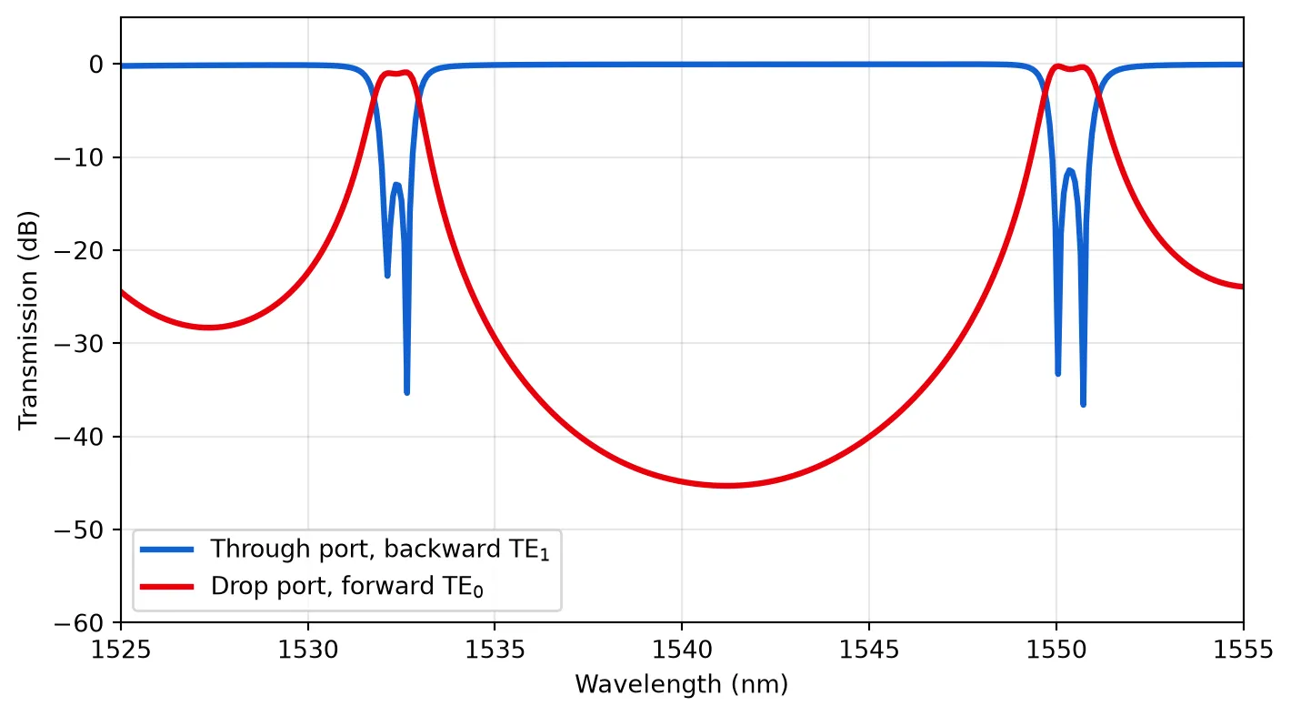
The through port sits near 0 dB right across the window, so the gratings reflect almost everything: with a corrugation this deep the stop band is wider than the 30 nm plotted here. Inside it the drop port shows a comb of narrow flat-topped passbands about 18 nm apart. That spacing is the free spectral range of the coupled cavities, and it is the budget the channel comb has to fit into.
Each passband is the channel its stage takes; everything else continues to the next stage. The design uses the branch near 1532 nm, so everything below searches a 16 nm band around it, which holds exactly one resonance of the comb for every phase-section length used here.
Setting the channel wavelength with Lₜ
Section titled “Setting the channel wavelength with Lₜ”Every stage uses the same gratings, so the stop band never moves. What moves is the resonance inside it, and it is set by the round-trip phase of the two cavities, which is proportional to the phase-section length . The response is linear over the range of interest, so three points are enough to calibrate it.
Because the gratings are already simulated, each of these costs nothing but a circuit composition.
lt_sweep = [0.434, 0.564, 0.695]          # Phase section lengths to calibrate against (um)
# Re-assembling the circuit at each value is all that is needed.s_sweep = [mwg_cavity(lt=lt).s_matrix(freqs) for lt in lt_sweep]
The resonance of each cavity is the drop-port maximum inside the design band. Restricting the search to that band is what separates the branch being designed from its neighbour in the comb, which can be the stronger of the two.
channel_band = (1530.0, 1546.0)     # Band the comb is placed in, narrower than one free spectral rangein_band = (lam > channel_band[0]) & (lam < channel_band[1])
# Each cavity resonance is the strongest drop peak inside that band.peaks = [lam[in_band][np.argmax((np.abs(s[("P0@0", "P1@0")]) ** 2)[in_band])] for s in s_sweep]
# Straight line through the three points: this is the tuning calibration.slope, intercept = np.polyfit(np.array(lt_sweep) * 1e3, peaks, 1)print("resonances (nm):", np.round(peaks, 2))print(f"tuning slope: {slope:.4f} nm of wavelength per nm of Lt")
resonances (nm): [1532.58 1537.6 1543.15]tuning slope: 0.0405 nm of wavelength per nm of Ltfig, axs = plt.subplots(1, 2, figsize=(12, 4), tight_layout=True)
# Left: the three measured spectra, showing the resonance sliding through a fixed stop band.for lt, s, color in zip(lt_sweep, s_sweep, ("#1b5e20", "#e8850b", "#7030a0")): axs[0].plot(lam, 10 * np.log10(np.abs(s[("P0@0", "P1@0")]) ** 2), color=color, lw=1.8, label=f"$L_t$ = {lt * 1e3:.0f} nm")axs[0].set(xlim=(lam.min(), lam.max()), ylim=(-60, 5), xlabel="Wavelength (nm)", ylabel="Drop transmission (dB)")axs[0].grid(alpha=0.3)axs[0].legend(loc="lower left")
# Right: the calibration line the channel grid is built from.lt_fine = np.linspace(0.40, 0.73, 50) * 1e3axs[1].plot(lt_fine, np.polyval([slope, intercept], lt_fine), color="#e8850b", lw=2, label=f"fit, {slope:.3f} nm/nm")axs[1].plot(np.array(lt_sweep) * 1e3, peaks, "o", color="#1b5e20", ms=8, label="simulated")axs[1].set(xlabel="$L_t$ (nm)", ylabel="Resonance wavelength (nm)")axs[1].grid(alpha=0.3)axs[1].legend()plt.show()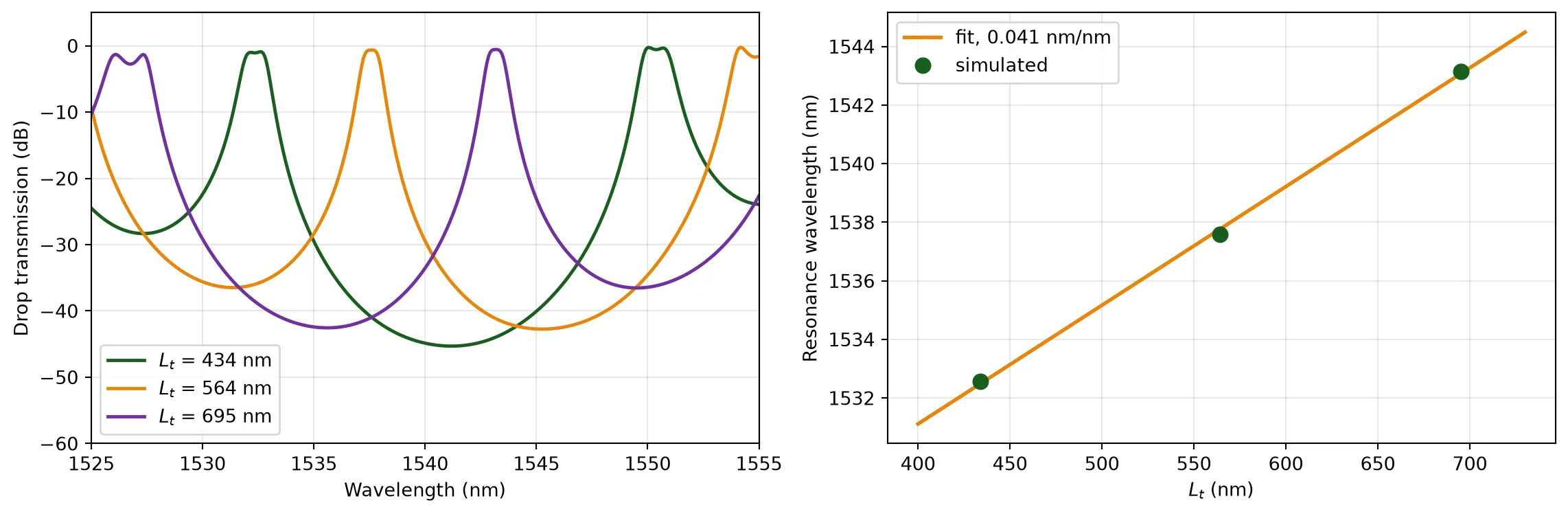
Eight channels from the calibration line
Section titled “Eight channels from the calibration line”The calibration converts a target channel grid into eight phase-section lengths. Evenly spaced gives an evenly spaced comb, so the eight values are simply spread across the calibrated range and rounded to the nanometre layout grid.
Each cavity is a circuit over the same two gratings, so the eight of them together add nothing to the simulation budget.
# Eight evenly spaced phase sections across the calibrated range, on the 1 nm layout grid.lt_channels = np.round(np.linspace(lt_sweep[0], lt_sweep[-1], 8), 3)print("Lt per channel (nm):", np.round(lt_channels * 1e3, 1))print(f"expected channel spacing: {slope * np.diff(lt_channels * 1e3)[0]:.2f} nm")
# One circuit per channel, over the gratings that are already simulated.cavities = [mwg_cavity(lt=lt) for lt in lt_channels]
Lt per channel (nm): [434. 471. 509. 546. 583. 620. 658. 695.]expected channel spacing: 1.50 nmMode demultiplexer
Section titled “Mode demultiplexer”Each stage needs a component that pulls backward TE₁ out of the multimode waveguide without disturbing forward TE₀. An adiabatic dual-core coupler does it: a narrow waveguide runs alongside a widening multimode waveguide, and along that taper the TE₁ supermode moves into the narrow waveguide while TE₀ stays where it is.
The coupling gap is set by the etch, not by the coupling strength. The ridge is 200 nm tall with 60 degree sidewalls, so each wall flares 116 nm outward between the top of the ridge and the slab. A gap drawn at 250 nm therefore closes to 19 nm where the two ridges meet the slab, which is below what the process can hold and below what the simulation grid can resolve. Drawn at 350 nm it is still 119 nm at the base, and the transfer has more room to stay adiabatic: the wider gap gives lower conversion loss and lower crosstalk than the tighter one.
Port A is the single-mode input, C is the multimode side facing the cavity, and B is the
narrow through port that feeds the next stage. Reading the device from C backwards: the narrow
waveguide starts at 0.2 µm, far from phase matching, then widens to 0.6 µm while the multimode
waveguide narrows from 2.0 µm to 1.0 µm, so TE₁ transfers across and emerges as TE₀ at
B. The narrow waveguide ends 2 µm short of the multimode end, where it carries no power.
@pf.parametric_componentdef mode_demux(    *,    w_in: float = 1.0,        # Single-mode input width of the wide waveguide (um)    w_mid: float = 1.2,       # Wide waveguide width at the start of the coupling section (um)    w_out: float = 2.0,       # Multimode width facing the cavity (um)    w_tap1: float = 0.6,      # Narrow waveguide width at the through port (um)    w_tap2: float = 0.2,      # Narrow waveguide width at the multimode end (um)    l_a: float = 50.0,        # Approach section length (um)    l_b: float = 100.0,       # Coupling section length (um)    l_c: float = 50.0,        # Separation section length (um)    gap_in: float = 2.25,     # Edge-to-edge gap at the input (um)    gap_mid: float = 0.35,    # Edge-to-edge gap through the coupling section (um)    gap_out: float = 1.25,    # Edge-to-edge gap where the narrow waveguide peels away (um)    l_tip: float = 2.0,       # How far short of the multimode end the narrow waveguide stops (um)) -> pf.Component:    """Adiabatic dual-core coupler: TE1 in the wide waveguide becomes TE0 in the narrow one."""
    # The wide waveguide widens monotonically from single mode to two modes.    x1, x2, x3 = l_a, l_a + l_b, l_a + l_b + l_c    wide = pf.Path((0, 0), w_in).segment((x1, 0), w_mid).segment((x2, 0), w_out).segment((x3, 0))
    # Centre lines of the narrow waveguide, set by the edge-to-edge gap at each station.    y0 = 0.5 * w_in + gap_in + 0.5 * w_tap1    y1 = 0.5 * w_mid + gap_mid + 0.5 * w_tap1    y2 = 0.5 * w_out + gap_mid + 0.5 * w_tap2    y3 = 0.5 * w_out + gap_out + 0.5 * w_tap2
    # The narrow waveguide comes in, runs alongside while narrowing, then peels away and stops.    narrow = pf.Path((0, y0), w_tap1).s_bend((x1, y1)).segment((x2, y2), w_tap2).s_bend((x3 - l_tip, y3))
    c = pf.Component("MODE_DEMUX")    c.add("RIDGE", wide, narrow)
    # Detect the three waveguide ends; they come back in the order the specs are listed.    port_a, port_b, port_c = c.detect_ports(["SM_1000", "SM_600", "MM_2000"], on_boundary="x")    c.add_port(port_a, port_name="A")    c.add_port(port_b, port_name="B")    c.add_port(port_c, port_name="C")
    c.add_model(pf.Tidy3DModel(verbose=False))    return c
mux = mode_demux()viewer(mux)
This is the one component in the design whose waveguides are not straight: the narrow one follows
two long shallow S-bends. Eigenmode expansion represents a device as a stack of uniform cells, so a
gradual lateral offset needs a great many of them, while FDTD handles it directly. The mode
demultiplexer therefore uses FDTD, and the straight transitions further down use eigenmode
expansion. Only two excitations matter in the cascade, forward TE₀ at A and backward TE₁
at C. They are evaluated on the coarse frequency grid because the response is
smooth, and stored as a DataModel so the circuit solve
interpolates instead of re-simulating.
# Two excitations on a coarse grid are enough for a response this smooth.s_mux = mux.s_matrix(freqs_coarse, model_kwargs={"inputs": ("A@0", "C@1")})mux.add_model(pf.DataModel(s_mux, interpolation_method="cubicspline"), "FDTD data")
# The two wanted paths and the two crosstalk paths of the device.lam_mux = s_mux.wavelengths * 1e3curves = {    "C TE$_1$ to B TE$_0$, rejected light to the next stage": np.abs(s_mux[("C@1", "B@0")]) ** 2,    "A TE$_0$ to C TE$_0$, input into the cavity": np.abs(s_mux[("A@0", "C@0")]) ** 2,    "C TE$_1$ to A TE$_0$, crosstalk": np.abs(s_mux[("C@1", "A@0")]) ** 2,    "A TE$_0$ to B TE$_0$, crosstalk": np.abs(s_mux[("A@0", "B@0")]) ** 2,}
fig, ax = plt.subplots(figsize=(7.5, 4), tight_layout=True)for label, value in curves.items():    ax.plot(lam_mux, 10 * np.log10(np.maximum(value, 1e-8)), lw=1.8, label=label)ax.set(xlabel="Wavelength (nm)", ylabel="Transmission (dB)", ylim=(-50, 2))ax.grid(alpha=0.3)ax.legend(fontsize=8, loc="lower right")plt.show()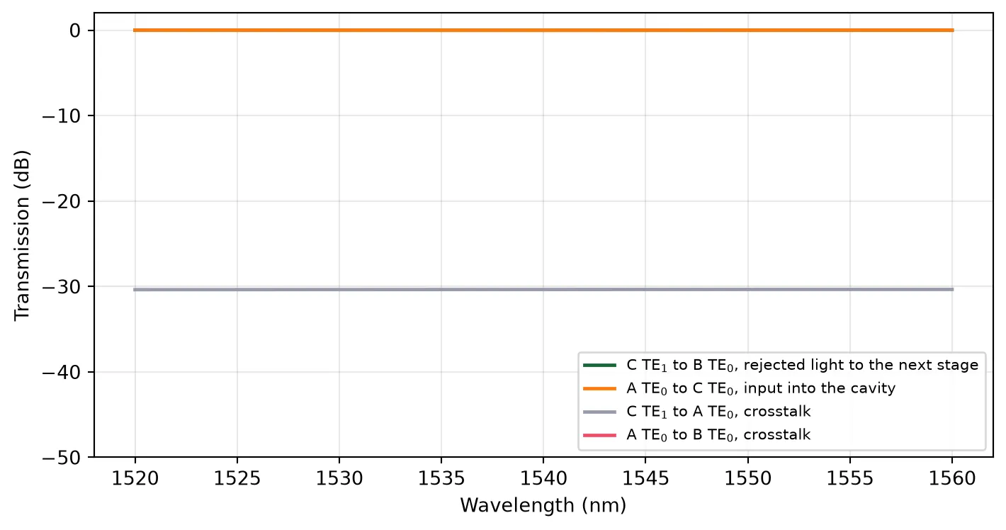
Width transitions
Section titled “Width transitions”Three width transitions connect the pieces: the multimode end of the demultiplexer to the slightly narrower grating waveguide, the grating waveguide to the single-mode drop waveguide, and the narrow through waveguide back to the demultiplexer input. They are straight and adiabatic, which is the regime where eigenmode expansion is both accurate and far cheaper than FDTD, so they use an EMEModel. All three come out lossless at the hundredth-of-a-decibel level, so they contribute nothing to the channel budget. The cell reports the departure from unit transmission rather than a signed loss, because at that level the numerical floor of the eigenmode expansion is the larger effect.
# Uniform EME grids; longer transitions need more cells to follow the width change.mode_spec = td.EMEModeSpec(num_modes=8)eme = dict(grid_spec=20, verbose=False)tapers = {    "mux to cavity": pf.parametric.transition(        port_spec1="MM_2000", port_spec2="MM_1850", length=5.0, name="TAPER_MUX_CAVITY",        model=pf.EMEModel(eme_grid_spec=td.EMEUniformGrid(num_cells=12, mode_spec=mode_spec), **eme)),    "cavity to drop": pf.parametric.transition(        port_spec1="MM_1850", port_spec2="SM_600", length=25.0, name="TAPER_DROP",        model=pf.EMEModel(eme_grid_spec=td.EMEUniformGrid(num_cells=30, mode_spec=mode_spec), **eme)),    "through to mux": pf.parametric.transition(        port_spec1="SM_600", port_spec2="SM_1000", length=15.0, name="TAPER_THROUGH",        model=pf.EMEModel(eme_grid_spec=td.EMEUniformGrid(num_cells=15, mode_spec=mode_spec), **eme)),}
# Run each transition once and store the result, so the circuit solve reads data instead of solving.for label, taper in tapers.items():    s = taper.s_matrix(freqs_coarse)    taper.add_model(pf.DataModel(s, interpolation_method="cubicspline"), "EME data")    # Worst departure from unit TE0 transmission across the band.    loss = -10 * np.log10(np.abs(s[("P0@0", "P1@0")]) ** 2)    print(f"{label}: TE0 insertion loss within {np.abs(loss).max():.3f} dB of zero")
viewer(tapers["cavity to drop"])
mux to cavity: TE0 insertion loss within 0.001 dB of zerocavity to drop: TE0 insertion loss within 0.001 dB of zero14:32:36 -03 WARNING: Warning messages were found in the solver log. For more information, check 'SimulationData.log' or use 'web.download_log(task_id)'.
through to mux: TE0 insertion loss within 0.007 dB of zero
Cascading eight stages
Section titled “Cascading eight stages”Each stage is a mode demultiplexer, a transition, a cavity, and a drop transition. The through port of one stage feeds the input of the next, so the stages stack upward on a 250 µm pitch, which matches a standard fibre-array spacing and lets every drop port run straight out to its own coupler. The connections between stages are made with route.
A route is built from the same parametric straights and bends, so every piece of it arrives with a WaveguideModel already attached and the routes need no model of their own. That model applies phase and no loss, which suits these routes: at the 100 µm radius used here FDTD gives a negligible loss and reflection for a 90 degree bend, and the bend mode stays 99 percent TE, so neither radiation nor mode conversion matters. Even summed over the fourteen bends the longest path crosses, what is left out stays well under the per-channel drop loss.
pitch = 250.0          # Stage pitch (um), equal to the fibre-array pitchx_through = -180.0     # Where the through transition of each stage sits (um)
demux = pf.Component("LNOI_DWDM_8CH")routes = []prev_through = None
for k, cavity_k in enumerate(cavities):    y = k * pitch
    # Place the stage: demultiplexer, transition, cavity, drop transition.    r_mux = demux.add_reference(mux)    r_mux.translate((0, y))    r_in = demux.add_reference(tapers["mux to cavity"])    r_in.connect("P0", r_mux["C"])    r_cavity = demux.add_reference(cavity_k)    r_cavity.connect("P0", r_in["P1"])    r_drop = demux.add_reference(tapers["cavity to drop"])    r_drop.connect("P0", r_cavity["P1"])    demux.add_port(r_drop["P1"], port_name=f"OUT{k + 1}")
    if k == 0:        # The first stage takes the chip input directly.        demux.add_port(r_mux["A"], port_name="IN")    else:        # Later stages are fed by the previous through port, widened back to the input width.        r_through = demux.add_reference(tapers["through to mux"])        r_through.translate((x_through, y))        for port1, port2 in ((prev_through, r_through["P0"]), (r_through["P1"], r_mux["A"])):            route = pf.parametric.route(port1=port1, port2=port2, radius=100.0)            demux.add_reference(route)            routes.append(route)    prev_through = r_mux["B"]
# Whatever survives all eight stages leaves on the through port.demux.add_port(prev_through, port_name="THRU")demux.add_model(pf.CircuitModel(verbose=False), "Circuit")
print("ports:", list(demux.ports))print("size (um):", np.round(demux.size(), 1))viewer(demux)
ports: ['IN', 'OUT1', 'OUT2', 'OUT3', 'OUT4', 'OUT5', 'OUT6', 'OUT7', 'OUT8', 'THRU']size (um): [ 639.8 1757.3];fill:%23221f20;font-weight:bold;font-size:77.321200px;}.terminal{fill:none;stroke:%23805080;stroke-width:9.665150;}.dashed{stroke-dasharray:48.325750,28.995450;}.port{fill:none;stroke:%23805080;stroke-width:19.330300;}.virtual-connection{fill:none;stroke:%23907090;stroke-width:14.497725;}.layer_1_0{stroke:%23c00020;fill:url(%23pat-layer_1_0);fill-opacity:0.492;}.label_1_0{fill:%23c00020;}</style><defs><path id=%22port-symbol%22 class=%22port%22 d=%22M 0,-38.660600 L 57.990900,0 0,38.660600%22 /><path id=%22ref-port-symbol%22 class=%22port%22 style=%22stroke-opacity:0.33;%22 d=%22M 0,-28.995450 C 38.660600,-28.995450 38.660600,28.995450 0,28.995450%22 /><circle id=%22port-bend-symbol%22 style=%22stroke-width:0;stroke:none;fill:%23805080;fill-opacity:1;%22 cx=%220%22 cy=%220%22 r=%2217.397270%22 /><circle id=%22connection-symbol%22 style=%22stroke-width:0;stroke:none;fill:%23907090;fill-opacity:1;%22 cx=%220%22 cy=%220%22 r=%2220.296815%22 /><pattern id=%22pat-layer_1_0%22 patternUnits=%22userSpaceOnUse%22 width=%2248.325750%22 height=%2248.325750%22 patternTransform=%22translate(19.898838,27.978066)%22><line x1=%220%22 y1=%220%22 x2=%2248.325750%22 y2=%2248.325750%22 style=%22stroke:%23c00020;stroke-width:4.832575%22 /><line x1=%22-24.162875%22 y1=%2224.162875%22 x2=%2224.162875%22 y2=%2272.488625%22 style=%22stroke:%23c00020;stroke-width:4.832575%22 /><line x1=%2224.162875%22 y1=%22-24.162875%22 x2=%2272.488625%22 y2=%2224.162875%22 style=%22stroke:%23c00020;stroke-width:4.832575%22 /></pattern><g id=%22C1%22 data-name=%22MODE_DEMUX%22><path class=%22layer_1_0%22 d=%22M 0.000000,-0.500000 25.000000,-0.550000 50.000000,-0.600000 100.000000,-0.800000 150.000000,-1.000000 200.000000,-1.000000 200.000000,1.000000 150.000000,1.000000 100.000000,0.800000 50.000000,0.600000 25.000000,0.550000 0.000000,0.500000 z%22 /><path class=%22layer_1_0%22 d=%22M 0.000000,2.750000 2.083000,2.744000 4.167000,2.725000 6.250000,2.694000 8.333000,2.650000 10.415000,2.594000 12.497000,2.525000 14.579000,2.444000 16.660000,2.350000 18.741000,2.244000 20.821000,2.125000 22.900000,1.994000 24.978000,1.851000 27.060000,1.707000 29.143000,1.576000 31.227000,1.457000 33.311000,1.350000 35.396000,1.257000 37.481000,1.175000 39.567000,1.106000 41.653000,1.050000 43.740000,1.006000 45.826000,0.975000 47.913000,0.956000 50.001000,0.950000 100.000000,1.150000 150.000000,1.350000 154.002000,1.369000 158.003000,1.411000 162.004000,1.475000 166.004000,1.561000 170.004000,1.669000 174.004000,1.800000 178.002000,1.931000 182.001000,2.039000 186.000000,2.126000 190.000000,2.189000 194.000000,2.231000 198.000000,2.250000 198.000000,2.450000 193.998000,2.431000 189.997000,2.389000 185.996000,2.325000 181.996000,2.239000 177.996000,2.131000 173.996000,2.000000 169.998000,1.869000 165.999000,1.761000 162.000000,1.674000 158.000000,1.611000 154.000000,1.569000 150.000000,1.550000 100.000000,1.550000 49.999000,1.550000 47.917000,1.556000 45.833000,1.575000 43.750000,1.606000 41.667000,1.650000 39.585000,1.706000 37.503000,1.775000 35.421000,1.856000 33.340000,1.950000 31.259000,2.056000 29.179000,2.175000 27.100000,2.306000 25.022000,2.449000 22.940000,2.593000 20.857000,2.724000 18.773000,2.843000 16.689000,2.950000 14.604000,3.043000 12.519000,3.125000 10.433000,3.194000 8.347000,3.250000 6.260000,3.294000 4.174000,3.325000 2.087000,3.344000 0.000000,3.350000 z%22 /></g><g id=%22C10%22 data-name=%22route__FWN4KWWLCCBGKLYKKID6LAWWNWVRKVUKDGZMLWMHO3GIZJJPUI7A%22><use transform=%22translate(-280.000000 400.000000) rotate(90.000000)%22 href=%22%23C27%22 /><use transform=%22translate(0.000000 253.050000) rotate(180.000000)%22 href=%22%23C28%22 /><use transform=%22translate(-180.000000 253.050000) rotate(180.000000)%22 href=%22%23C27%22 /><use transform=%22translate(-280.000000 353.050000) rotate(90.000000)%22 href=%22%23C29%22 /></g><g id=%22C11%22 data-name=%22route__SCPG7NV3FSJNZW5YHARUGKH3AQJLJVM3VNZJH3JD5YTKO2LZRHPQ%22><use transform=%22translate(-165.000000 500.000000)%22 href=%22%23C30%22 /></g><g id=%22C12%22 data-name=%22MWG_CAVITY_LT546%22><use transform=%22translate(0.000000 0.000000)%22 href=%22%23C31%22 /><use transform=%22translate(1.400000 0.000000)%22 href=%22%23C32%22 /><use transform=%22translate(30.631000 0.000000)%22 href=%22%23C33%22 /><use transform=%22translate(30.977000 0.000000)%22 href=%22%23C34%22 /><use transform=%22translate(89.239000 0.000000)%22 href=%22%23C33%22 /><use transform=%22translate(89.585000 0.000000)%22 href=%22%23C32%22 /><use transform=%22translate(118.816000 0.000000)%22 href=%22%23C35%22 /></g><g id=%22C13%22 data-name=%22route__VH7ZTQFKEGHZ7TFEKSRHQ74XZRTV7ZNUE6HUL2V7DUAN6VNNLD2A%22><use transform=%22translate(-280.000000 650.000000) rotate(90.000000)%22 href=%22%23C27%22 /><use transform=%22translate(0.000000 503.050000) rotate(180.000000)%22 href=%22%23C28%22 /><use transform=%22translate(-180.000000 503.050000) rotate(180.000000)%22 href=%22%23C27%22 /><use transform=%22translate(-280.000000 603.050000) rotate(90.000000)%22 href=%22%23C29%22 /></g><g id=%22C14%22 data-name=%22route__IPVPFRIVXEZCVGZMC4DEX2CZOLGDBSG37OB4OBBGUHMAQMF3VBIQ%22><use transform=%22translate(-165.000000 750.000000)%22 href=%22%23C30%22 /></g><g id=%22C15%22 data-name=%22MWG_CAVITY_LT583%22><use transform=%22translate(0.000000 0.000000)%22 href=%22%23C31%22 /><use transform=%22translate(1.400000 0.000000)%22 href=%22%23C32%22 /><use transform=%22translate(30.631000 0.000000)%22 href=%22%23C36%22 /><use transform=%22translate(31.014000 0.000000)%22 href=%22%23C34%22 /><use transform=%22translate(89.276000 0.000000)%22 href=%22%23C36%22 /><use transform=%22translate(89.659000 0.000000)%22 href=%22%23C32%22 /><use transform=%22translate(118.890000 0.000000)%22 href=%22%23C35%22 /></g><g id=%22C16%22 data-name=%22route__PPQOPOTETB2MCZENG3RKI4VQ2QRXUFHX2EAWY7DZTU73MSITDXVA%22><use transform=%22translate(-280.000000 900.000000) rotate(90.000000)%22 href=%22%23C27%22 /><use transform=%22translate(0.000000 753.050000) rotate(180.000000)%22 href=%22%23C28%22 /><use transform=%22translate(-180.000000 753.050000) rotate(180.000000)%22 href=%22%23C27%22 /><use transform=%22translate(-280.000000 853.050000) rotate(90.000000)%22 href=%22%23C29%22 /></g><g id=%22C17%22 data-name=%22route__OPAIK6XHATNA4QPYHBIRUDXPU6A5HYKYOC7MNZKZDFQV3DYWYAFQ%22><use transform=%22translate(-165.000000 1000.000000)%22 href=%22%23C30%22 /></g><g id=%22C18%22 data-name=%22MWG_CAVITY_LT620%22><use transform=%22translate(0.000000 0.000000)%22 href=%22%23C31%22 /><use transform=%22translate(1.400000 0.000000)%22 href=%22%23C32%22 /><use transform=%22translate(30.631000 0.000000)%22 href=%22%23C37%22 /><use transform=%22translate(31.051000 0.000000)%22 href=%22%23C34%22 /><use transform=%22translate(89.313000 0.000000)%22 href=%22%23C37%22 /><use transform=%22translate(89.733000 0.000000)%22 href=%22%23C32%22 /><use transform=%22translate(118.964000 0.000000)%22 href=%22%23C35%22 /></g><g id=%22C19%22 data-name=%22route__WULUGARLGSUU3BQKL625WI2X3EEM2HD3YAFMBXRJLDCHC3HRMXSA%22><use transform=%22translate(-280.000000 1150.000000) rotate(90.000000)%22 href=%22%23C27%22 /><use transform=%22translate(0.000000 1003.050000) rotate(180.000000)%22 href=%22%23C28%22 /><use transform=%22translate(-180.000000 1003.050000) rotate(180.000000)%22 href=%22%23C27%22 /><use transform=%22translate(-280.000000 1103.050000) rotate(90.000000)%22 href=%22%23C29%22 /></g><g id=%22C2%22 data-name=%22TAPER_MUX_CAVITY%22><path class=%22layer_1_0%22 d=%22M 0.000000,-1.000000 1.000000,-0.985000 2.000000,-0.970000 3.000000,-0.955000 4.000000,-0.940000 5.000000,-0.925000 5.000000,0.925000 4.000000,0.940000 3.000000,0.955000 2.000000,0.970000 1.000000,0.985000 0.000000,1.000000 z%22 /></g><g id=%22C20%22 data-name=%22route__6KRJ4BSOPQR25SME2OP5MRCJM23WXY3WTLTYFQPF26PUZB2334LA%22><use transform=%22translate(-165.000000 1250.000000)%22 href=%22%23C30%22 /></g><g id=%22C21%22 data-name=%22MWG_CAVITY_LT658%22><use transform=%22translate(0.000000 0.000000)%22 href=%22%23C31%22 /><use transform=%22translate(1.400000 0.000000)%22 href=%22%23C32%22 /><use transform=%22translate(30.631000 0.000000)%22 href=%22%23C38%22 /><use transform=%22translate(31.089000 0.000000)%22 href=%22%23C34%22 /><use transform=%22translate(89.351000 0.000000)%22 href=%22%23C38%22 /><use transform=%22translate(89.809000 0.000000)%22 href=%22%23C32%22 /><use transform=%22translate(119.040000 0.000000)%22 href=%22%23C35%22 /></g><g id=%22C22%22 data-name=%22route__BKKCSPPSZBDARBXJD4NSSHV4KIHQ3CQZG4BQKHWLPZZPXUATICTQ%22><use transform=%22translate(-280.000000 1400.000000) rotate(90.000000)%22 href=%22%23C27%22 /><use transform=%22translate(0.000000 1253.050000) rotate(180.000000)%22 href=%22%23C28%22 /><use transform=%22translate(-180.000000 1253.050000) rotate(180.000000)%22 href=%22%23C27%22 /><use transform=%22translate(-280.000000 1353.050000) rotate(90.000000)%22 href=%22%23C29%22 /></g><g id=%22C23%22 data-name=%22route__F5UNXUHSCZJX3ZXUCP5OLXWQBO4I2YPMKIOXWKD6YSWVTGKG54CA%22><use transform=%22translate(-165.000000 1500.000000)%22 href=%22%23C30%22 /></g><g id=%22C24%22 data-name=%22MWG_CAVITY_LT695%22><use transform=%22translate(0.000000 0.000000)%22 href=%22%23C31%22 /><use transform=%22translate(1.400000 0.000000)%22 href=%22%23C32%22 /><use transform=%22translate(30.631000 0.000000)%22 href=%22%23C39%22 /><use transform=%22translate(31.126000 0.000000)%22 href=%22%23C34%22 /><use transform=%22translate(89.388000 0.000000)%22 href=%22%23C39%22 /><use transform=%22translate(89.883000 0.000000)%22 href=%22%23C32%22 /><use transform=%22translate(119.114000 0.000000)%22 href=%22%23C35%22 /></g><g id=%22C25%22 data-name=%22route__ZEEMPG2CIPSBBI2TWAA4TZ64ZI32EPMIJYUKTR5I2NBMMFA5ZB3A%22><use transform=%22translate(-280.000000 1650.000000) rotate(90.000000)%22 href=%22%23C27%22 /><use transform=%22translate(0.000000 1503.050000) rotate(180.000000)%22 href=%22%23C28%22 /><use transform=%22translate(-180.000000 1503.050000) rotate(180.000000)%22 href=%22%23C27%22 /><use transform=%22translate(-280.000000 1603.050000) rotate(90.000000)%22 href=%22%23C29%22 /></g><g id=%22C26%22 data-name=%22route__TPN4JCR5C6Y2TQBNGFZILECGGOIQ232QYDVTNBHTOUNYR4EVN5HQ%22><use transform=%22translate(-165.000000 1750.000000)%22 href=%22%23C30%22 /></g><g id=%22C3%22 data-name=%22MWG_CAVITY_LT434%22><use transform=%22translate(0.000000 0.000000)%22 href=%22%23C31%22 /><use transform=%22translate(1.400000 0.000000)%22 href=%22%23C32%22 /><use transform=%22translate(30.631000 0.000000)%22 href=%22%23C40%22 /><use transform=%22translate(30.865000 0.000000)%22 href=%22%23C34%22 /><use transform=%22translate(89.127000 0.000000)%22 href=%22%23C40%22 /><use transform=%22translate(89.361000 0.000000)%22 href=%22%23C32%22 /><use transform=%22translate(118.592000 0.000000)%22 href=%22%23C35%22 /></g><g id=%22C4%22 data-name=%22TAPER_DROP%22><path class=%22layer_1_0%22 d=%22M 0.000000,-0.925000 5.000000,-0.800000 10.000000,-0.675000 15.000000,-0.550000 20.000000,-0.425000 25.000000,-0.300000 25.000000,0.300000 20.000000,0.425000 15.000000,0.550000 10.000000,0.675000 5.000000,0.800000 0.000000,0.925000 z%22 /></g><g id=%22C5%22 data-name=%22MWG_CAVITY_LT471%22><use transform=%22translate(0.000000 0.000000)%22 href=%22%23C31%22 /><use transform=%22translate(1.400000 0.000000)%22 href=%22%23C32%22 /><use transform=%22translate(30.631000 0.000000)%22 href=%22%23C41%22 /><use transform=%22translate(30.902000 0.000000)%22 href=%22%23C34%22 /><use transform=%22translate(89.164000 0.000000)%22 href=%22%23C41%22 /><use transform=%22translate(89.435000 0.000000)%22 href=%22%23C32%22 /><use transform=%22translate(118.666000 0.000000)%22 href=%22%23C35%22 /></g><g id=%22C6%22 data-name=%22TAPER_THROUGH%22><path class=%22layer_1_0%22 d=%22M 0.000000,-0.300000 3.000000,-0.340000 6.000000,-0.380000 9.000000,-0.420000 12.000000,-0.460000 15.000000,-0.500000 15.000000,0.500000 12.000000,0.460000 9.000000,0.420000 6.000000,0.380000 3.000000,0.340000 0.000000,0.300000 z%22 /></g><g id=%22C7%22 data-name=%22route__VA6BJHOYHC63QIZ445GA6YCQ4D6CFQ6FYUD2WBZ55TJ6QUZOXCAQ%22><use transform=%22translate(-280.000000 150.000000) rotate(90.000000)%22 href=%22%23C27%22 /><use transform=%22translate(0.000000 3.050000) rotate(180.000000)%22 href=%22%23C28%22 /><use transform=%22translate(-180.000000 3.050000) rotate(180.000000)%22 href=%22%23C27%22 /><use transform=%22translate(-280.000000 103.050000) rotate(90.000000)%22 href=%22%23C29%22 /></g><g id=%22C8%22 data-name=%22route__7PHWFB4XMCSUI3V4KMAKVV4OHL4NSMX3QKY3IBWDSXE3XR3HUBUQ%22><use transform=%22translate(-165.000000 250.000000)%22 href=%22%23C30%22 /></g><g id=%22C9%22 data-name=%22MWG_CAVITY_LT509%22><use transform=%22translate(0.000000 0.000000)%22 href=%22%23C31%22 /><use transform=%22translate(1.400000 0.000000)%22 href=%22%23C32%22 /><use transform=%22translate(30.631000 0.000000)%22 href=%22%23C42%22 /><use transform=%22translate(30.940000 0.000000)%22 href=%22%23C34%22 /><use transform=%22translate(89.202000 0.000000)%22 href=%22%23C42%22 /><use transform=%22translate(89.511000 0.000000)%22 href=%22%23C32%22 /><use transform=%22translate(118.742000 0.000000)%22 href=%22%23C35%22 /></g><g id=%22C27%22 data-name=%22bend__IKK4DHLUGL2VXXMLIUH6AUSDFGFKQCPCAEBQGLKIYSUAWAUNTJVA%22><path class=%22layer_1_0%22 d=%22M 0.000000,-0.300000 2.008000,-0.320000 3.011000,-0.345000 5.017000,-0.426000 6.020000,-0.482000 8.023000,-0.623000 9.023000,-0.709000 10.022000,-0.805000 12.018000,-1.027000 14.008000,-1.289000 15.001000,-1.435000 15.993000,-1.591000 16.983000,-1.757000 17.971000,-1.933000 18.958000,-2.119000 19.943000,-2.315000 21.906000,-2.736000 23.860000,-3.197000 24.833000,-3.442000 25.804000,-3.697000 27.738000,-4.236000 28.701000,-4.520000 29.661000,-4.814000 31.572000,-5.431000 33.470000,-6.086000 35.354000,-6.779000 37.224000,-7.510000 38.154000,-7.889000 40.001000,-8.676000 41.832000,-9.500000 42.741000,-9.926000 44.546000,-10.805000 45.442000,-11.258000 46.333000,-11.720000 48.101000,-12.671000 49.850000,-13.657000 51.579000,-14.679000 52.435000,-15.202000 54.132000,-16.275000 55.807000,-17.382000 57.459000,-18.523000 58.277000,-19.106000 59.894000,-20.296000 60.694000,-20.903000 62.274000,-22.141000 63.055000,-22.772000 64.597000,-24.057000 66.113000,-25.373000 67.603000,-26.720000 69.065000,-28.096000 70.499000,-29.501000 71.904000,-30.935000 73.280000,-32.397000 74.627000,-33.887000 75.943000,-35.403000 77.228000,-36.945000 78.482000,-38.513000 79.097000,-39.306000 80.303000,-40.912000 80.894000,-41.723000 81.477000,-42.541000 82.618000,-44.193000 83.725000,-45.868000 84.798000,-47.565000 85.836000,-49.283000 86.343000,-50.150000 87.329000,-51.899000 88.280000,-53.667000 88.742000,-54.558000 89.195000,-55.454000 90.074000,-57.259000 90.500000,-58.168000 91.324000,-59.999000 92.111000,-61.846000 92.860000,-63.709000 93.221000,-64.646000 93.914000,-66.530000 94.569000,-68.428000 95.186000,-70.339000 95.480000,-71.299000 95.764000,-72.262000 96.303000,-74.196000 96.558000,-75.167000 96.803000,-76.140000 97.264000,-78.094000 97.685000,-80.057000 97.881000,-81.042000 98.067000,-82.029000 98.243000,-83.017000 98.409000,-84.007000 98.565000,-84.999000 98.711000,-85.992000 98.973000,-87.982000 99.089000,-88.980000 99.195000,-89.978000 99.291000,-90.977000 99.377000,-91.977000 99.518000,-93.980000 99.574000,-94.983000 99.655000,-96.989000 99.680000,-97.992000 99.700000,-100.000000 100.300000,-100.000000 100.280000,-97.980000 100.219000,-95.961000 100.173000,-94.952000 100.051000,-92.936000 99.975000,-91.929000 99.792000,-89.918000 99.569000,-87.910000 99.442000,-86.908000 99.158000,-84.908000 99.001000,-83.911000 98.834000,-82.915000 98.657000,-81.920000 98.470000,-80.928000 98.273000,-79.937000 98.066000,-78.949000 97.849000,-77.963000 97.622000,-76.978000 97.139000,-75.017000 96.616000,-73.066000 96.340000,-72.095000 95.759000,-70.160000 95.453000,-69.198000 94.814000,-67.282000 94.136000,-65.379000 93.782000,-64.433000 93.047000,-62.552000 92.274000,-60.686000 91.464000,-58.836000 90.616000,-57.002000 90.179000,-56.092000 89.732000,-55.186000 88.811000,-53.388000 87.855000,-51.609000 87.363000,-50.727000 86.353000,-48.978000 85.835000,-48.111000 84.773000,-46.393000 84.229000,-45.542000 83.115000,-43.857000 82.545000,-43.023000 81.381000,-41.372000 80.787000,-40.556000 80.184000,-39.746000 78.955000,-38.143000 78.328000,-37.351000 77.693000,-36.566000 76.400000,-35.014000 75.742000,-34.248000 75.076000,-33.489000 73.721000,-31.990000 72.337000,-30.520000 70.923000,-29.077000 69.480000,-27.663000 68.010000,-26.279000 67.264000,-25.598000 65.752000,-24.258000 64.986000,-23.600000 64.213000,-22.950000 62.649000,-21.672000 61.857000,-21.045000 61.059000,-20.427000 59.444000,-19.213000 58.628000,-18.619000 57.805000,-18.033000 56.143000,-16.885000 54.458000,-15.771000 53.607000,-15.227000 51.889000,-14.165000 51.022000,-13.647000 49.273000,-12.637000 48.391000,-12.145000 46.612000,-11.189000 44.814000,-10.268000 43.908000,-9.821000 42.998000,-9.384000 41.164000,-8.536000 39.314000,-7.726000 37.448000,-6.953000 36.509000,-6.581000 34.621000,-5.864000 32.718000,-5.186000 31.762000,-4.862000 29.840000,-4.241000 27.905000,-3.660000 26.934000,-3.384000 24.983000,-2.861000 23.022000,-2.378000 21.051000,-1.934000 20.063000,-1.727000 19.072000,-1.530000 18.080000,-1.343000 17.085000,-1.166000 16.089000,-0.999000 15.092000,-0.842000 13.092000,-0.558000 12.090000,-0.431000 10.082000,-0.208000 8.071000,-0.025000 7.064000,0.051000 5.048000,0.173000 4.039000,0.219000 2.020000,0.280000 0.000000,0.300000 z%22 /></g><g id=%22C28%22 data-name=%22straight__YKFXTSDSQWC4F26FCCMTGT7OEYVHT7CBPQUTQYX2TRWKSZZHQWCQ%22><path class=%22layer_1_0%22 d=%22M 0.000000,-0.300000 180.000000,-0.300000 180.000000,0.300000 0.000000,0.300000 z%22 /></g><g id=%22C29%22 data-name=%22straight__NHC5YYKNNH2EGMIIPPWHSPHPKTOV5HQDVGQ66UNSBLEXXDMZQB7A%22><path class=%22layer_1_0%22 d=%22M 0.000000,-0.300000 46.950000,-0.300000 46.950000,0.300000 0.000000,0.300000 z%22 /></g><g id=%22C30%22 data-name=%22straight__GYKC5OFIZY5WWUK6MVWE2JIUWEJ2F7WMUJWHSJY7SY43VFTUPEPA%22><path class=%22layer_1_0%22 d=%22M 0.000000,-0.500000 165.000000,-0.500000 165.000000,0.500000 0.000000,0.500000 z%22 /></g><g id=%22C31%22 data-name=%22straight__HZELSZ7Y6PQG3I45LHLPVZQLT3BZEGPLWJAWJROFJKRP6B2ZENMA%22><path class=%22layer_1_0%22 d=%22M 0.000000,-0.925000 1.400000,-0.925000 1.400000,0.925000 0.000000,0.925000 z%22 /></g><g id=%22C32%22 data-name=%22GRATING_67%22><path class=%22layer_1_0%22 d=%22M 0.000000,-0.925000 0.100000,-0.925000 0.100000,-0.873000 0.317000,-0.873000 0.317000,-0.977000 0.533000,-0.977000 0.533000,-0.865000 0.750000,-0.865000 0.750000,-0.985000 0.967000,-0.985000 0.967000,-0.856000 1.183000,-0.856000 1.183000,-0.994000 1.400000,-0.994000 1.400000,-0.846000 1.617000,-0.846000 1.617000,-1.004000 1.833000,-1.004000 1.833000,-0.835000 2.050000,-0.835000 2.050000,-1.015000 2.267000,-1.015000 2.267000,-0.823000 2.483000,-0.823000 2.483000,-1.027000 2.700000,-1.027000 2.700000,-0.810000 2.916000,-0.810000 2.916000,-1.040000 3.133000,-1.040000 3.133000,-0.796000 3.350000,-0.796000 3.350000,-1.054000 3.566000,-1.054000 3.566000,-0.781000 3.783000,-0.781000 3.783000,-1.069000 4.000000,-1.069000 4.000000,-0.764000 4.216000,-0.764000 4.216000,-1.086000 4.433000,-1.086000 4.433000,-0.747000 4.650000,-0.747000 4.650000,-1.103000 4.866000,-1.103000 4.866000,-0.729000 5.083000,-0.729000 5.083000,-1.121000 5.300000,-1.121000 5.300000,-0.709000 5.516000,-0.709000 5.516000,-1.141000 5.733000,-1.141000 5.733000,-0.689000 5.950000,-0.689000 5.950000,-1.161000 6.166000,-1.161000 6.166000,-0.668000 6.383000,-0.668000 6.383000,-1.182000 6.600000,-1.182000 6.600000,-0.647000 6.816000,-0.647000 6.816000,-1.203000 7.033000,-1.203000 7.033000,-0.625000 7.249000,-0.625000 7.249000,-1.225000 7.466000,-1.225000 7.466000,-0.603000 7.683000,-0.603000 7.683000,-1.247000 7.899000,-1.247000 7.899000,-0.581000 8.116000,-0.581000 8.116000,-1.269000 8.333000,-1.269000 8.333000,-0.559000 8.549000,-0.559000 8.549000,-1.291000 8.766000,-1.291000 8.766000,-0.537000 8.983000,-0.537000 8.983000,-1.313000 9.199000,-1.313000 9.199000,-0.515000 9.416000,-0.515000 9.416000,-1.335000 9.633000,-1.335000 9.633000,-0.495000 9.849000,-0.495000 9.849000,-1.355000 10.066000,-1.355000 10.066000,-0.475000 10.283000,-0.475000 10.283000,-1.375000 10.499000,-1.375000 10.499000,-0.457000 10.716000,-0.457000 10.716000,-1.393000 10.933000,-1.393000 10.933000,-0.440000 11.149000,-0.440000 11.149000,-1.410000 11.366000,-1.410000 11.366000,-0.424000 11.582000,-0.424000 11.582000,-1.426000 11.799000,-1.426000 11.799000,-0.411000 12.016000,-0.411000 12.016000,-1.439000 12.232000,-1.439000 12.232000,-0.399000 12.449000,-0.399000 12.449000,-1.451000 12.666000,-1.451000 12.666000,-0.390000 12.882000,-0.390000 12.882000,-1.460000 13.099000,-1.460000 13.099000,-0.383000 13.316000,-0.383000 13.316000,-1.467000 13.532000,-1.467000 13.532000,-0.378000 13.749000,-0.378000 13.749000,-1.472000 13.966000,-1.472000 13.966000,-0.375000 14.182000,-0.375000 14.182000,-1.475000 14.399000,-1.475000 14.399000,-0.375000 14.616000,-0.375000 14.616000,-1.475000 14.832000,-1.475000 14.832000,-0.378000 15.049000,-0.378000 15.049000,-1.472000 15.266000,-1.472000 15.266000,-0.383000 15.482000,-0.383000 15.482000,-1.467000 15.699000,-1.467000 15.699000,-0.390000 15.915000,-0.390000 15.915000,-1.460000 16.132000,-1.460000 16.132000,-0.399000 16.349000,-0.399000 16.349000,-1.451000 16.565000,-1.451000 16.565000,-0.411000 16.782000,-0.411000 16.782000,-1.439000 16.999000,-1.439000 16.999000,-0.424000 17.215000,-0.424000 17.215000,-1.426000 17.432000,-1.426000 17.432000,-0.440000 17.649000,-0.440000 17.649000,-1.410000 17.865000,-1.410000 17.865000,-0.457000 18.082000,-0.457000 18.082000,-1.393000 18.299000,-1.393000 18.299000,-0.475000 18.515000,-0.475000 18.515000,-1.375000 18.732000,-1.375000 18.732000,-0.495000 18.949000,-0.495000 18.949000,-1.355000 19.165000,-1.355000 19.165000,-0.515000 19.382000,-0.515000 19.382000,-1.335000 19.599000,-1.335000 19.599000,-0.537000 19.815000,-0.537000 19.815000,-1.313000 20.032000,-1.313000 20.032000,-0.559000 20.248000,-0.559000 20.248000,-1.291000 20.465000,-1.291000 20.465000,-0.581000 20.682000,-0.581000 20.682000,-1.269000 20.898000,-1.269000 20.898000,-0.603000 21.115000,-0.603000 21.115000,-1.247000 21.332000,-1.247000 21.332000,-0.625000 21.548000,-0.625000 21.548000,-1.225000 21.765000,-1.225000 21.765000,-0.647000 21.982000,-0.647000 21.982000,-1.203000 22.198000,-1.203000 22.198000,-0.668000 22.415000,-0.668000 22.415000,-1.182000 22.632000,-1.182000 22.632000,-0.689000 22.848000,-0.689000 22.848000,-1.161000 23.065000,-1.161000 23.065000,-0.709000 23.282000,-0.709000 23.282000,-1.141000 23.498000,-1.141000 23.498000,-0.729000 23.715000,-0.729000 23.715000,-1.121000 23.932000,-1.121000 23.932000,-0.747000 24.148000,-0.747000 24.148000,-1.103000 24.365000,-1.103000 24.365000,-0.764000 24.581000,-0.764000 24.581000,-1.086000 24.798000,-1.086000 24.798000,-0.781000 25.015000,-0.781000 25.015000,-1.069000 25.231000,-1.069000 25.231000,-0.796000 25.448000,-0.796000 25.448000,-1.054000 25.665000,-1.054000 25.665000,-0.810000 25.881000,-0.810000 25.881000,-1.040000 26.098000,-1.040000 26.098000,-0.823000 26.315000,-0.823000 26.315000,-1.027000 26.531000,-1.027000 26.531000,-0.835000 26.748000,-0.835000 26.748000,-1.015000 26.965000,-1.015000 26.965000,-0.846000 27.181000,-0.846000 27.181000,-1.004000 27.398000,-1.004000 27.398000,-0.856000 27.615000,-0.856000 27.615000,-0.994000 27.831000,-0.994000 27.831000,-0.865000 28.048000,-0.865000 28.048000,-0.985000 28.265000,-0.985000 28.265000,-0.873000 28.481000,-0.873000 28.481000,-0.977000 28.698000,-0.977000 28.698000,-0.880000 28.914000,-0.880000 28.914000,-0.970000 29.131000,-0.970000 29.131000,-0.925000 29.231000,-0.925000 29.231000,0.925000 29.131000,0.925000 29.131000,0.880000 28.914000,0.880000 28.914000,0.970000 28.698000,0.970000 28.698000,0.873000 28.481000,0.873000 28.481000,0.977000 28.265000,0.977000 28.265000,0.865000 28.048000,0.865000 28.048000,0.985000 27.831000,0.985000 27.831000,0.856000 27.615000,0.856000 27.615000,0.994000 27.398000,0.994000 27.398000,0.846000 27.181000,0.846000 27.181000,1.004000 26.965000,1.004000 26.965000,0.835000 26.748000,0.835000 26.748000,1.015000 26.531000,1.015000 26.531000,0.823000 26.315000,0.823000 26.315000,1.027000 26.098000,1.027000 26.098000,0.810000 25.881000,0.810000 25.881000,1.040000 25.665000,1.040000 25.665000,0.796000 25.448000,0.796000 25.448000,1.054000 25.231000,1.054000 25.231000,0.781000 25.015000,0.781000 25.015000,1.069000 24.798000,1.069000 24.798000,0.764000 24.581000,0.764000 24.581000,1.086000 24.365000,1.086000 24.365000,0.747000 24.148000,0.747000 24.148000,1.103000 23.932000,1.103000 23.932000,0.729000 23.715000,0.729000 23.715000,1.121000 23.498000,1.121000 23.498000,0.709000 23.282000,0.709000 23.282000,1.141000 23.065000,1.141000 23.065000,0.689000 22.848000,0.689000 22.848000,1.161000 22.632000,1.161000 22.632000,0.668000 22.415000,0.668000 22.415000,1.182000 22.198000,1.182000 22.198000,0.647000 21.982000,0.647000 21.982000,1.203000 21.765000,1.203000 21.765000,0.625000 21.548000,0.625000 21.548000,1.225000 21.332000,1.225000 21.332000,0.603000 21.115000,0.603000 21.115000,1.247000 20.898000,1.247000 20.898000,0.581000 20.682000,0.581000 20.682000,1.269000 20.465000,1.269000 20.465000,0.559000 20.248000,0.559000 20.248000,1.291000 20.032000,1.291000 20.032000,0.537000 19.815000,0.537000 19.815000,1.313000 19.599000,1.313000 19.599000,0.515000 19.382000,0.515000 19.382000,1.335000 19.165000,1.335000 19.165000,0.495000 18.949000,0.495000 18.949000,1.355000 18.732000,1.355000 18.732000,0.475000 18.515000,0.475000 18.515000,1.375000 18.299000,1.375000 18.299000,0.457000 18.082000,0.457000 18.082000,1.393000 17.865000,1.393000 17.865000,0.440000 17.649000,0.440000 17.649000,1.410000 17.432000,1.410000 17.432000,0.424000 17.215000,0.424000 17.215000,1.426000 16.999000,1.426000 16.999000,0.411000 16.782000,0.411000 16.782000,1.439000 16.565000,1.439000 16.565000,0.399000 16.349000,0.399000 16.349000,1.451000 16.132000,1.451000 16.132000,0.390000 15.915000,0.390000 15.915000,1.460000 15.699000,1.460000 15.699000,0.383000 15.482000,0.383000 15.482000,1.467000 15.266000,1.467000 15.266000,0.378000 15.049000,0.378000 15.049000,1.472000 14.832000,1.472000 14.832000,0.375000 14.616000,0.375000 14.616000,1.475000 14.399000,1.475000 14.399000,0.375000 14.182000,0.375000 14.182000,1.475000 13.966000,1.475000 13.966000,0.378000 13.749000,0.378000 13.749000,1.472000 13.532000,1.472000 13.532000,0.383000 13.316000,0.383000 13.316000,1.467000 13.099000,1.467000 13.099000,0.390000 12.882000,0.390000 12.882000,1.460000 12.666000,1.460000 12.666000,0.399000 12.449000,0.399000 12.449000,1.451000 12.232000,1.451000 12.232000,0.411000 12.016000,0.411000 12.016000,1.439000 11.799000,1.439000 11.799000,0.424000 11.582000,0.424000 11.582000,1.426000 11.366000,1.426000 11.366000,0.440000 11.149000,0.440000 11.149000,1.410000 10.933000,1.410000 10.933000,0.457000 10.716000,0.457000 10.716000,1.393000 10.499000,1.393000 10.499000,0.475000 10.283000,0.475000 10.283000,1.375000 10.066000,1.375000 10.066000,0.495000 9.849000,0.495000 9.849000,1.355000 9.633000,1.355000 9.633000,0.515000 9.416000,0.515000 9.416000,1.335000 9.199000,1.335000 9.199000,0.537000 8.983000,0.537000 8.983000,1.313000 8.766000,1.313000 8.766000,0.559000 8.549000,0.559000 8.549000,1.291000 8.333000,1.291000 8.333000,0.581000 8.116000,0.581000 8.116000,1.269000 7.899000,1.269000 7.899000,0.603000 7.683000,0.603000 7.683000,1.247000 7.466000,1.247000 7.466000,0.625000 7.249000,0.625000 7.249000,1.225000 7.033000,1.225000 7.033000,0.647000 6.816000,0.647000 6.816000,1.203000 6.600000,1.203000 6.600000,0.668000 6.383000,0.668000 6.383000,1.182000 6.166000,1.182000 6.166000,0.689000 5.950000,0.689000 5.950000,1.161000 5.733000,1.161000 5.733000,0.709000 5.516000,0.709000 5.516000,1.141000 5.300000,1.141000 5.300000,0.729000 5.083000,0.729000 5.083000,1.121000 4.866000,1.121000 4.866000,0.747000 4.650000,0.747000 4.650000,1.103000 4.433000,1.103000 4.433000,0.764000 4.216000,0.764000 4.216000,1.086000 4.000000,1.086000 4.000000,0.781000 3.783000,0.781000 3.783000,1.069000 3.566000,1.069000 3.566000,0.796000 3.350000,0.796000 3.350000,1.054000 3.133000,1.054000 3.133000,0.810000 2.916000,0.810000 2.916000,1.040000 2.700000,1.040000 2.700000,0.823000 2.483000,0.823000 2.483000,1.027000 2.267000,1.027000 2.267000,0.835000 2.050000,0.835000 2.050000,1.015000 1.833000,1.015000 1.833000,0.846000 1.617000,0.846000 1.617000,1.004000 1.400000,1.004000 1.400000,0.856000 1.183000,0.856000 1.183000,0.994000 0.967000,0.994000 0.967000,0.865000 0.750000,0.865000 0.750000,0.985000 0.533000,0.985000 0.533000,0.873000 0.317000,0.873000 0.317000,0.977000 0.100000,0.977000 0.100000,0.925000 0.000000,0.925000 z%22 /></g><g id=%22C33%22 data-name=%22straight__JW7YSUY6Z535CT2QTSKG2WHIKHTZK63MO67OIN7HU3CQ7WFDBOUA%22><path class=%22layer_1_0%22 d=%22M 0.000000,-0.925000 0.346000,-0.925000 0.346000,0.925000 0.000000,0.925000 z%22 /></g><g id=%22C34%22 data-name=%22GRATING_134%22><path class=%22layer_1_0%22 d=%22M 0.000000,-0.925000 0.100000,-0.925000 0.100000,-0.876000 0.317000,-0.876000 0.317000,-0.974000 0.533000,-0.974000 0.533000,-0.873000 0.750000,-0.873000 0.750000,-0.977000 0.967000,-0.977000 0.967000,-0.869000 1.183000,-0.869000 1.183000,-0.981000 1.400000,-0.981000 1.400000,-0.865000 1.617000,-0.865000 1.617000,-0.985000 1.833000,-0.985000 1.833000,-0.860000 2.050000,-0.860000 2.050000,-0.990000 2.267000,-0.990000 2.267000,-0.856000 2.483000,-0.856000 2.483000,-0.994000 2.700000,-0.994000 2.700000,-0.851000 2.916000,-0.851000 2.916000,-0.999000 3.133000,-0.999000 3.133000,-0.846000 3.350000,-0.846000 3.350000,-1.004000 3.566000,-1.004000 3.566000,-0.841000 3.783000,-0.841000 3.783000,-1.009000 4.000000,-1.009000 4.000000,-0.835000 4.216000,-0.835000 4.216000,-1.015000 4.433000,-1.015000 4.433000,-0.829000 4.650000,-0.829000 4.650000,-1.021000 4.866000,-1.021000 4.866000,-0.823000 5.083000,-0.823000 5.083000,-1.027000 5.300000,-1.027000 5.300000,-0.817000 5.516000,-0.817000 5.516000,-1.033000 5.733000,-1.033000 5.733000,-0.810000 5.950000,-0.810000 5.950000,-1.040000 6.166000,-1.040000 6.166000,-0.803000 6.383000,-0.803000 6.383000,-1.047000 6.600000,-1.047000 6.600000,-0.796000 6.816000,-0.796000 6.816000,-1.054000 7.033000,-1.054000 7.033000,-0.788000 7.249000,-0.788000 7.249000,-1.062000 7.466000,-1.062000 7.466000,-0.781000 7.683000,-0.781000 7.683000,-1.069000 7.899000,-1.069000 7.899000,-0.773000 8.116000,-0.773000 8.116000,-1.077000 8.333000,-1.077000 8.333000,-0.764000 8.549000,-0.764000 8.549000,-1.086000 8.766000,-1.086000 8.766000,-0.756000 8.983000,-0.756000 8.983000,-1.094000 9.199000,-1.094000 9.199000,-0.747000 9.416000,-0.747000 9.416000,-1.103000 9.633000,-1.103000 9.633000,-0.738000 9.849000,-0.738000 9.849000,-1.112000 10.066000,-1.112000 10.066000,-0.729000 10.283000,-0.729000 10.283000,-1.121000 10.499000,-1.121000 10.499000,-0.719000 10.716000,-0.719000 10.716000,-1.131000 10.933000,-1.131000 10.933000,-0.709000 11.149000,-0.709000 11.149000,-1.141000 11.366000,-1.141000 11.366000,-0.699000 11.582000,-0.699000 11.582000,-1.151000 11.799000,-1.151000 11.799000,-0.689000 12.016000,-0.689000 12.016000,-1.161000 12.232000,-1.161000 12.232000,-0.679000 12.449000,-0.679000 12.449000,-1.171000 12.666000,-1.171000 12.666000,-0.668000 12.882000,-0.668000 12.882000,-1.182000 13.099000,-1.182000 13.099000,-0.658000 13.316000,-0.658000 13.316000,-1.192000 13.532000,-1.192000 13.532000,-0.647000 13.749000,-0.647000 13.749000,-1.203000 13.966000,-1.203000 13.966000,-0.636000 14.182000,-0.636000 14.182000,-1.214000 14.399000,-1.214000 14.399000,-0.625000 14.616000,-0.625000 14.616000,-1.225000 14.832000,-1.225000 14.832000,-0.614000 15.049000,-0.614000 15.049000,-1.236000 15.266000,-1.236000 15.266000,-0.603000 15.482000,-0.603000 15.482000,-1.247000 15.699000,-1.247000 15.699000,-0.592000 15.915000,-0.592000 15.915000,-1.258000 16.132000,-1.258000 16.132000,-0.581000 16.349000,-0.581000 16.349000,-1.269000 16.565000,-1.269000 16.565000,-0.570000 16.782000,-0.570000 16.782000,-1.280000 16.999000,-1.280000 16.999000,-0.559000 17.215000,-0.559000 17.215000,-1.291000 17.432000,-1.291000 17.432000,-0.548000 17.649000,-0.548000 17.649000,-1.302000 17.865000,-1.302000 17.865000,-0.537000 18.082000,-0.537000 18.082000,-1.313000 18.299000,-1.313000 18.299000,-0.526000 18.515000,-0.526000 18.515000,-1.324000 18.732000,-1.324000 18.732000,-0.515000 18.949000,-0.515000 18.949000,-1.335000 19.165000,-1.335000 19.165000,-0.505000 19.382000,-0.505000 19.382000,-1.345000 19.599000,-1.345000 19.599000,-0.495000 19.815000,-0.495000 19.815000,-1.355000 20.032000,-1.355000 20.032000,-0.485000 20.248000,-0.485000 20.248000,-1.365000 20.465000,-1.365000 20.465000,-0.475000 20.682000,-0.475000 20.682000,-1.375000 20.898000,-1.375000 20.898000,-0.466000 21.115000,-0.466000 21.115000,-1.384000 21.332000,-1.384000 21.332000,-0.457000 21.548000,-0.457000 21.548000,-1.393000 21.765000,-1.393000 21.765000,-0.448000 21.982000,-0.448000 21.982000,-1.402000 22.198000,-1.402000 22.198000,-0.440000 22.415000,-0.440000 22.415000,-1.410000 22.632000,-1.410000 22.632000,-0.432000 22.848000,-0.432000 22.848000,-1.418000 23.065000,-1.418000 23.065000,-0.424000 23.282000,-0.424000 23.282000,-1.426000 23.498000,-1.426000 23.498000,-0.417000 23.715000,-0.417000 23.715000,-1.433000 23.932000,-1.433000 23.932000,-0.411000 24.148000,-0.411000 24.148000,-1.439000 24.365000,-1.439000 24.365000,-0.405000 24.581000,-0.405000 24.581000,-1.445000 24.798000,-1.445000 24.798000,-0.399000 25.015000,-0.399000 25.015000,-1.451000 25.231000,-1.451000 25.231000,-0.394000 25.448000,-0.394000 25.448000,-1.456000 25.665000,-1.456000 25.665000,-0.390000 25.881000,-0.390000 25.881000,-1.460000 26.098000,-1.460000 26.098000,-0.386000 26.315000,-0.386000 26.315000,-1.464000 26.531000,-1.464000 26.531000,-0.383000 26.748000,-0.383000 26.748000,-1.467000 26.965000,-1.467000 26.965000,-0.380000 27.181000,-0.380000 27.181000,-1.470000 27.398000,-1.470000 27.398000,-0.378000 27.615000,-0.378000 27.615000,-1.472000 27.831000,-1.472000 27.831000,-0.376000 28.048000,-0.376000 28.048000,-1.474000 28.265000,-1.474000 28.265000,-0.375000 28.481000,-0.375000 28.481000,-1.475000 28.698000,-1.475000 28.698000,-0.375000 28.914000,-0.375000 28.914000,-1.475000 29.131000,-1.475000 29.131000,-0.375000 29.348000,-0.375000 29.348000,-1.475000 29.564000,-1.475000 29.564000,-0.376000 29.781000,-0.376000 29.781000,-1.474000 29.998000,-1.474000 29.998000,-0.378000 30.214000,-0.378000 30.214000,-1.472000 30.431000,-1.472000 30.431000,-0.380000 30.648000,-0.380000 30.648000,-1.470000 30.864000,-1.470000 30.864000,-0.383000 31.081000,-0.383000 31.081000,-1.467000 31.298000,-1.467000 31.298000,-0.386000 31.514000,-0.386000 31.514000,-1.464000 31.731000,-1.464000 31.731000,-0.390000 31.948000,-0.390000 31.948000,-1.460000 32.164000,-1.460000 32.164000,-0.394000 32.381000,-0.394000 32.381000,-1.456000 32.598000,-1.456000 32.598000,-0.399000 32.814000,-0.399000 32.814000,-1.451000 33.031000,-1.451000 33.031000,-0.405000 33.247000,-0.405000 33.247000,-1.445000 33.464000,-1.445000 33.464000,-0.411000 33.681000,-0.411000 33.681000,-1.439000 33.897000,-1.439000 33.897000,-0.417000 34.114000,-0.417000 34.114000,-1.433000 34.331000,-1.433000 34.331000,-0.424000 34.547000,-0.424000 34.547000,-1.426000 34.764000,-1.426000 34.764000,-0.432000 34.981000,-0.432000 34.981000,-1.418000 35.197000,-1.418000 35.197000,-0.440000 35.414000,-0.440000 35.414000,-1.410000 35.631000,-1.410000 35.631000,-0.448000 35.847000,-0.448000 35.847000,-1.402000 36.064000,-1.402000 36.064000,-0.457000 36.281000,-0.457000 36.281000,-1.393000 36.497000,-1.393000 36.497000,-0.466000 36.714000,-0.466000 36.714000,-1.384000 36.931000,-1.384000 36.931000,-0.475000 37.147000,-0.475000 37.147000,-1.375000 37.364000,-1.375000 37.364000,-0.485000 37.580000,-0.485000 37.580000,-1.365000 37.797000,-1.365000 37.797000,-0.495000 38.014000,-0.495000 38.014000,-1.355000 38.230000,-1.355000 38.230000,-0.505000 38.447000,-0.505000 38.447000,-1.345000 38.664000,-1.345000 38.664000,-0.515000 38.880000,-0.515000 38.880000,-1.335000 39.097000,-1.335000 39.097000,-0.526000 39.314000,-0.526000 39.314000,-1.324000 39.530000,-1.324000 39.530000,-0.537000 39.747000,-0.537000 39.747000,-1.313000 39.964000,-1.313000 39.964000,-0.548000 40.180000,-0.548000 40.180000,-1.302000 40.397000,-1.302000 40.397000,-0.559000 40.614000,-0.559000 40.614000,-1.291000 40.830000,-1.291000 40.830000,-0.570000 41.047000,-0.570000 41.047000,-1.280000 41.264000,-1.280000 41.264000,-0.581000 41.480000,-0.581000 41.480000,-1.269000 41.697000,-1.269000 41.697000,-0.592000 41.913000,-0.592000 41.913000,-1.258000 42.130000,-1.258000 42.130000,-0.603000 42.347000,-0.603000 42.347000,-1.247000 42.563000,-1.247000 42.563000,-0.614000 42.780000,-0.614000 42.780000,-1.236000 42.997000,-1.236000 42.997000,-0.625000 43.213000,-0.625000 43.213000,-1.225000 43.430000,-1.225000 43.430000,-0.636000 43.647000,-0.636000 43.647000,-1.214000 43.863000,-1.214000 43.863000,-0.647000 44.080000,-0.647000 44.080000,-1.203000 44.297000,-1.203000 44.297000,-0.658000 44.513000,-0.658000 44.513000,-1.192000 44.730000,-1.192000 44.730000,-0.668000 44.947000,-0.668000 44.947000,-1.182000 45.163000,-1.182000 45.163000,-0.679000 45.380000,-0.679000 45.380000,-1.171000 45.597000,-1.171000 45.597000,-0.689000 45.813000,-0.689000 45.813000,-1.161000 46.030000,-1.161000 46.030000,-0.699000 46.246000,-0.699000 46.246000,-1.151000 46.463000,-1.151000 46.463000,-0.709000 46.680000,-0.709000 46.680000,-1.141000 46.896000,-1.141000 46.896000,-0.719000 47.113000,-0.719000 47.113000,-1.131000 47.330000,-1.131000 47.330000,-0.729000 47.546000,-0.729000 47.546000,-1.121000 47.763000,-1.121000 47.763000,-0.738000 47.980000,-0.738000 47.980000,-1.112000 48.196000,-1.112000 48.196000,-0.747000 48.413000,-0.747000 48.413000,-1.103000 48.630000,-1.103000 48.630000,-0.756000 48.846000,-0.756000 48.846000,-1.094000 49.063000,-1.094000 49.063000,-0.764000 49.280000,-0.764000 49.280000,-1.086000 49.496000,-1.086000 49.496000,-0.773000 49.713000,-0.773000 49.713000,-1.077000 49.930000,-1.077000 49.930000,-0.781000 50.146000,-0.781000 50.146000,-1.069000 50.363000,-1.069000 50.363000,-0.788000 50.579000,-0.788000 50.579000,-1.062000 50.796000,-1.062000 50.796000,-0.796000 51.013000,-0.796000 51.013000,-1.054000 51.229000,-1.054000 51.229000,-0.803000 51.446000,-0.803000 51.446000,-1.047000 51.663000,-1.047000 51.663000,-0.810000 51.879000,-0.810000 51.879000,-1.040000 52.096000,-1.040000 52.096000,-0.817000 52.313000,-0.817000 52.313000,-1.033000 52.529000,-1.033000 52.529000,-0.823000 52.746000,-0.823000 52.746000,-1.027000 52.963000,-1.027000 52.963000,-0.829000 53.179000,-0.829000 53.179000,-1.021000 53.396000,-1.021000 53.396000,-0.835000 53.613000,-0.835000 53.613000,-1.015000 53.829000,-1.015000 53.829000,-0.841000 54.046000,-0.841000 54.046000,-1.009000 54.263000,-1.009000 54.263000,-0.846000 54.479000,-0.846000 54.479000,-1.004000 54.696000,-1.004000 54.696000,-0.851000 54.912000,-0.851000 54.912000,-0.999000 55.129000,-0.999000 55.129000,-0.856000 55.346000,-0.856000 55.346000,-0.994000 55.562000,-0.994000 55.562000,-0.860000 55.779000,-0.860000 55.779000,-0.990000 55.996000,-0.990000 55.996000,-0.865000 56.212000,-0.865000 56.212000,-0.985000 56.429000,-0.985000 56.429000,-0.869000 56.646000,-0.869000 56.646000,-0.981000 56.862000,-0.981000 56.862000,-0.873000 57.079000,-0.873000 57.079000,-0.977000 57.296000,-0.977000 57.296000,-0.876000 57.512000,-0.876000 57.512000,-0.974000 57.729000,-0.974000 57.729000,-0.880000 57.946000,-0.880000 57.946000,-0.970000 58.162000,-0.970000 58.162000,-0.925000 58.262000,-0.925000 58.262000,0.925000 58.162000,0.925000 58.162000,0.880000 57.946000,0.880000 57.946000,0.970000 57.729000,0.970000 57.729000,0.876000 57.512000,0.876000 57.512000,0.974000 57.296000,0.974000 57.296000,0.873000 57.079000,0.873000 57.079000,0.977000 56.862000,0.977000 56.862000,0.869000 56.646000,0.869000 56.646000,0.981000 56.429000,0.981000 56.429000,0.865000 56.212000,0.865000 56.212000,0.985000 55.996000,0.985000 55.996000,0.860000 55.779000,0.860000 55.779000,0.990000 55.562000,0.990000 55.562000,0.856000 55.346000,0.856000 55.346000,0.994000 55.129000,0.994000 55.129000,0.851000 54.912000,0.851000 54.912000,0.999000 54.696000,0.999000 54.696000,0.846000 54.479000,0.846000 54.479000,1.004000 54.263000,1.004000 54.263000,0.841000 54.046000,0.841000 54.046000,1.009000 53.829000,1.009000 53.829000,0.835000 53.613000,0.835000 53.613000,1.015000 53.396000,1.015000 53.396000,0.829000 53.179000,0.829000 53.179000,1.021000 52.963000,1.021000 52.963000,0.823000 52.746000,0.823000 52.746000,1.027000 52.529000,1.027000 52.529000,0.817000 52.313000,0.817000 52.313000,1.033000 52.096000,1.033000 52.096000,0.810000 51.879000,0.810000 51.879000,1.040000 51.663000,1.040000 51.663000,0.803000 51.446000,0.803000 51.446000,1.047000 51.229000,1.047000 51.229000,0.796000 51.013000,0.796000 51.013000,1.054000 50.796000,1.054000 50.796000,0.788000 50.579000,0.788000 50.579000,1.062000 50.363000,1.062000 50.363000,0.781000 50.146000,0.781000 50.146000,1.069000 49.930000,1.069000 49.930000,0.773000 49.713000,0.773000 49.713000,1.077000 49.496000,1.077000 49.496000,0.764000 49.280000,0.764000 49.280000,1.086000 49.063000,1.086000 49.063000,0.756000 48.846000,0.756000 48.846000,1.094000 48.630000,1.094000 48.630000,0.747000 48.413000,0.747000 48.413000,1.103000 48.196000,1.103000 48.196000,0.738000 47.980000,0.738000 47.980000,1.112000 47.763000,1.112000 47.763000,0.729000 47.546000,0.729000 47.546000,1.121000 47.330000,1.121000 47.330000,0.719000 47.113000,0.719000 47.113000,1.131000 46.896000,1.131000 46.896000,0.709000 46.680000,0.709000 46.680000,1.141000 46.463000,1.141000 46.463000,0.699000 46.246000,0.699000 46.246000,1.151000 46.030000,1.151000 46.030000,0.689000 45.813000,0.689000 45.813000,1.161000 45.597000,1.161000 45.597000,0.679000 45.380000,0.679000 45.380000,1.171000 45.163000,1.171000 45.163000,0.668000 44.947000,0.668000 44.947000,1.182000 44.730000,1.182000 44.730000,0.658000 44.513000,0.658000 44.513000,1.192000 44.297000,1.192000 44.297000,0.647000 44.080000,0.647000 44.080000,1.203000 43.863000,1.203000 43.863000,0.636000 43.647000,0.636000 43.647000,1.214000 43.430000,1.214000 43.430000,0.625000 43.213000,0.625000 43.213000,1.225000 42.997000,1.225000 42.997000,0.614000 42.780000,0.614000 42.780000,1.236000 42.563000,1.236000 42.563000,0.603000 42.347000,0.603000 42.347000,1.247000 42.130000,1.247000 42.130000,0.592000 41.913000,0.592000 41.913000,1.258000 41.697000,1.258000 41.697000,0.581000 41.480000,0.581000 41.480000,1.269000 41.264000,1.269000 41.264000,0.570000 41.047000,0.570000 41.047000,1.280000 40.830000,1.280000 40.830000,0.559000 40.614000,0.559000 40.614000,1.291000 40.397000,1.291000 40.397000,0.548000 40.180000,0.548000 40.180000,1.302000 39.964000,1.302000 39.964000,0.537000 39.747000,0.537000 39.747000,1.313000 39.530000,1.313000 39.530000,0.526000 39.314000,0.526000 39.314000,1.324000 39.097000,1.324000 39.097000,0.515000 38.880000,0.515000 38.880000,1.335000 38.664000,1.335000 38.664000,0.505000 38.447000,0.505000 38.447000,1.345000 38.230000,1.345000 38.230000,0.495000 38.014000,0.495000 38.014000,1.355000 37.797000,1.355000 37.797000,0.485000 37.580000,0.485000 37.580000,1.365000 37.364000,1.365000 37.364000,0.475000 37.147000,0.475000 37.147000,1.375000 36.931000,1.375000 36.931000,0.466000 36.714000,0.466000 36.714000,1.384000 36.497000,1.384000 36.497000,0.457000 36.281000,0.457000 36.281000,1.393000 36.064000,1.393000 36.064000,0.448000 35.847000,0.448000 35.847000,1.402000 35.631000,1.402000 35.631000,0.440000 35.414000,0.440000 35.414000,1.410000 35.197000,1.410000 35.197000,0.432000 34.981000,0.432000 34.981000,1.418000 34.764000,1.418000 34.764000,0.424000 34.547000,0.424000 34.547000,1.426000 34.331000,1.426000 34.331000,0.417000 34.114000,0.417000 34.114000,1.433000 33.897000,1.433000 33.897000,0.411000 33.681000,0.411000 33.681000,1.439000 33.464000,1.439000 33.464000,0.405000 33.247000,0.405000 33.247000,1.445000 33.031000,1.445000 33.031000,0.399000 32.814000,0.399000 32.814000,1.451000 32.598000,1.451000 32.598000,0.394000 32.381000,0.394000 32.381000,1.456000 32.164000,1.456000 32.164000,0.390000 31.948000,0.390000 31.948000,1.460000 31.731000,1.460000 31.731000,0.386000 31.514000,0.386000 31.514000,1.464000 31.298000,1.464000 31.298000,0.383000 31.081000,0.383000 31.081000,1.467000 30.864000,1.467000 30.864000,0.380000 30.648000,0.380000 30.648000,1.470000 30.431000,1.470000 30.431000,0.378000 30.214000,0.378000 30.214000,1.472000 29.998000,1.472000 29.998000,0.376000 29.781000,0.376000 29.781000,1.474000 29.564000,1.474000 29.564000,0.375000 29.348000,0.375000 29.348000,1.475000 29.131000,1.475000 29.131000,0.375000 28.914000,0.375000 28.914000,1.475000 28.698000,1.475000 28.698000,0.375000 28.481000,0.375000 28.481000,1.475000 28.265000,1.475000 28.265000,0.376000 28.048000,0.376000 28.048000,1.474000 27.831000,1.474000 27.831000,0.378000 27.615000,0.378000 27.615000,1.472000 27.398000,1.472000 27.398000,0.380000 27.181000,0.380000 27.181000,1.470000 26.965000,1.470000 26.965000,0.383000 26.748000,0.383000 26.748000,1.467000 26.531000,1.467000 26.531000,0.386000 26.315000,0.386000 26.315000,1.464000 26.098000,1.464000 26.098000,0.390000 25.881000,0.390000 25.881000,1.460000 25.665000,1.460000 25.665000,0.394000 25.448000,0.394000 25.448000,1.456000 25.231000,1.456000 25.231000,0.399000 25.015000,0.399000 25.015000,1.451000 24.798000,1.451000 24.798000,0.405000 24.581000,0.405000 24.581000,1.445000 24.365000,1.445000 24.365000,0.411000 24.148000,0.411000 24.148000,1.439000 23.932000,1.439000 23.932000,0.417000 23.715000,0.417000 23.715000,1.433000 23.498000,1.433000 23.498000,0.424000 23.282000,0.424000 23.282000,1.426000 23.065000,1.426000 23.065000,0.432000 22.848000,0.432000 22.848000,1.418000 22.632000,1.418000 22.632000,0.440000 22.415000,0.440000 22.415000,1.410000 22.198000,1.410000 22.198000,0.448000 21.982000,0.448000 21.982000,1.402000 21.765000,1.402000 21.765000,0.457000 21.548000,0.457000 21.548000,1.393000 21.332000,1.393000 21.332000,0.466000 21.115000,0.466000 21.115000,1.384000 20.898000,1.384000 20.898000,0.475000 20.682000,0.475000 20.682000,1.375000 20.465000,1.375000 20.465000,0.485000 20.248000,0.485000 20.248000,1.365000 20.032000,1.365000 20.032000,0.495000 19.815000,0.495000 19.815000,1.355000 19.599000,1.355000 19.599000,0.505000 19.382000,0.505000 19.382000,1.345000 19.165000,1.345000 19.165000,0.515000 18.949000,0.515000 18.949000,1.335000 18.732000,1.335000 18.732000,0.526000 18.515000,0.526000 18.515000,1.324000 18.299000,1.324000 18.299000,0.537000 18.082000,0.537000 18.082000,1.313000 17.865000,1.313000 17.865000,0.548000 17.649000,0.548000 17.649000,1.302000 17.432000,1.302000 17.432000,0.559000 17.215000,0.559000 17.215000,1.291000 16.999000,1.291000 16.999000,0.570000 16.782000,0.570000 16.782000,1.280000 16.565000,1.280000 16.565000,0.581000 16.349000,0.581000 16.349000,1.269000 16.132000,1.269000 16.132000,0.592000 15.915000,0.592000 15.915000,1.258000 15.699000,1.258000 15.699000,0.603000 15.482000,0.603000 15.482000,1.247000 15.266000,1.247000 15.266000,0.614000 15.049000,0.614000 15.049000,1.236000 14.832000,1.236000 14.832000,0.625000 14.616000,0.625000 14.616000,1.225000 14.399000,1.225000 14.399000,0.636000 14.182000,0.636000 14.182000,1.214000 13.966000,1.214000 13.966000,0.647000 13.749000,0.647000 13.749000,1.203000 13.532000,1.203000 13.532000,0.658000 13.316000,0.658000 13.316000,1.192000 13.099000,1.192000 13.099000,0.668000 12.882000,0.668000 12.882000,1.182000 12.666000,1.182000 12.666000,0.679000 12.449000,0.679000 12.449000,1.171000 12.232000,1.171000 12.232000,0.689000 12.016000,0.689000 12.016000,1.161000 11.799000,1.161000 11.799000,0.699000 11.582000,0.699000 11.582000,1.151000 11.366000,1.151000 11.366000,0.709000 11.149000,0.709000 11.149000,1.141000 10.933000,1.141000 10.933000,0.719000 10.716000,0.719000 10.716000,1.131000 10.499000,1.131000 10.499000,0.729000 10.283000,0.729000 10.283000,1.121000 10.066000,1.121000 10.066000,0.738000 9.849000,0.738000 9.849000,1.112000 9.633000,1.112000 9.633000,0.747000 9.416000,0.747000 9.416000,1.103000 9.199000,1.103000 9.199000,0.756000 8.983000,0.756000 8.983000,1.094000 8.766000,1.094000 8.766000,0.764000 8.549000,0.764000 8.549000,1.086000 8.333000,1.086000 8.333000,0.773000 8.116000,0.773000 8.116000,1.077000 7.899000,1.077000 7.899000,0.781000 7.683000,0.781000 7.683000,1.069000 7.466000,1.069000 7.466000,0.788000 7.249000,0.788000 7.249000,1.062000 7.033000,1.062000 7.033000,0.796000 6.816000,0.796000 6.816000,1.054000 6.600000,1.054000 6.600000,0.803000 6.383000,0.803000 6.383000,1.047000 6.166000,1.047000 6.166000,0.810000 5.950000,0.810000 5.950000,1.040000 5.733000,1.040000 5.733000,0.817000 5.516000,0.817000 5.516000,1.033000 5.300000,1.033000 5.300000,0.823000 5.083000,0.823000 5.083000,1.027000 4.866000,1.027000 4.866000,0.829000 4.650000,0.829000 4.650000,1.021000 4.433000,1.021000 4.433000,0.835000 4.216000,0.835000 4.216000,1.015000 4.000000,1.015000 4.000000,0.841000 3.783000,0.841000 3.783000,1.009000 3.566000,1.009000 3.566000,0.846000 3.350000,0.846000 3.350000,1.004000 3.133000,1.004000 3.133000,0.851000 2.916000,0.851000 2.916000,0.999000 2.700000,0.999000 2.700000,0.856000 2.483000,0.856000 2.483000,0.994000 2.267000,0.994000 2.267000,0.860000 2.050000,0.860000 2.050000,0.990000 1.833000,0.990000 1.833000,0.865000 1.617000,0.865000 1.617000,0.985000 1.400000,0.985000 1.400000,0.869000 1.183000,0.869000 1.183000,0.981000 0.967000,0.981000 0.967000,0.873000 0.750000,0.873000 0.750000,0.977000 0.533000,0.977000 0.533000,0.876000 0.317000,0.876000 0.317000,0.974000 0.100000,0.974000 0.100000,0.925000 0.000000,0.925000 z%22 /></g><g id=%22C35%22 data-name=%22straight__TQCYPPIAXQXSY4ITNS5VI2JBUSJT6SY4NZR6C272KHK54NTP55VA%22><path class=%22layer_1_0%22 d=%22M 0.000000,-0.925000 10.400000,-0.925000 10.400000,0.925000 0.000000,0.925000 z%22 /></g><g id=%22C36%22 data-name=%22straight__BLM24DZCJOBAIVUC5WUKG2N3UHMCDFMWQQCP57QQR5D6OQ342THQ%22><path class=%22layer_1_0%22 d=%22M 0.000000,-0.925000 0.383000,-0.925000 0.383000,0.925000 0.000000,0.925000 z%22 /></g><g id=%22C37%22 data-name=%22straight__C4CTYA76GGTSZ7IIR7MAOHASCGVCYFDWE6LFZA6EBMSNZ7XD5DDA%22><path class=%22layer_1_0%22 d=%22M 0.000000,-0.925000 0.420000,-0.925000 0.420000,0.925000 0.000000,0.925000 z%22 /></g><g id=%22C38%22 data-name=%22straight__YVPG7YLRDJOVVR7YCQGPOSZFGTM324WZFRIFAO2JCS2HX7IAQVVQ%22><path class=%22layer_1_0%22 d=%22M 0.000000,-0.925000 0.458000,-0.925000 0.458000,0.925000 0.000000,0.925000 z%22 /></g><g id=%22C39%22 data-name=%22straight__KEDAHKULLEIININVI3NMHIL4SEAJWHUERF42KAV7W42ZU6LC2DXQ%22><path class=%22layer_1_0%22 d=%22M 0.000000,-0.925000 0.495000,-0.925000 0.495000,0.925000 0.000000,0.925000 z%22 /></g><g id=%22C40%22 data-name=%22straight__3DIPTEFGIVEVI53Y6BKQACHWGANGXTONM6ONWOTYXHU7IU2R5JPA%22><path class=%22layer_1_0%22 d=%22M 0.000000,-0.925000 0.234000,-0.925000 0.234000,0.925000 0.000000,0.925000 z%22 /></g><g id=%22C41%22 data-name=%22straight__GNICNN4OIDOONCHZV5GEGLBJGI52BOBFGXSQ5C4B5Z3GRNGKQPUA%22><path class=%22layer_1_0%22 d=%22M 0.000000,-0.925000 0.271000,-0.925000 0.271000,0.925000 0.000000,0.925000 z%22 /></g><g id=%22C42%22 data-name=%22straight__6OYWZOL526FZMZ3NRRN5Y2HLIB3ZJMY4DT2E652H77O72CVTPA2Q%22><path class=%22layer_1_0%22 d=%22M 0.000000,-0.925000 0.309000,-0.925000 0.309000,0.925000 0.000000,0.925000 z%22 /></g></defs><g transform=%22scale(1 -1)%22><g id=%22C0%22 data-name=%22LNOI_DWDM_8CH%22><use transform=%22translate(0.000000 0.000000)%22 href=%22%23C1%22 /><use transform=%22translate(200.000000 0.000000)%22 href=%22%23C2%22 /><use transform=%22translate(205.000000 0.000000)%22 href=%22%23C3%22 /><use transform=%22translate(333.992000 0.000000)%22 href=%22%23C4%22 /><use transform=%22translate(0.000000 250.000000)%22 href=%22%23C1%22 /><use transform=%22translate(200.000000 250.000000)%22 href=%22%23C2%22 /><use transform=%22translate(205.000000 250.000000)%22 href=%22%23C5%22 /><use transform=%22translate(334.066000 250.000000)%22 href=%22%23C4%22 /><use transform=%22translate(-180.000000 250.000000)%22 href=%22%23C6%22 /><use transform=%22translate(0.000000 0.000000)%22 href=%22%23C7%22 /><use transform=%22translate(0.000000 0.000000)%22 href=%22%23C8%22 /><use transform=%22translate(0.000000 500.000000)%22 href=%22%23C1%22 /><use transform=%22translate(200.000000 500.000000)%22 href=%22%23C2%22 /><use transform=%22translate(205.000000 500.000000)%22 href=%22%23C9%22 /><use transform=%22translate(334.142000 500.000000)%22 href=%22%23C4%22 /><use transform=%22translate(-180.000000 500.000000)%22 href=%22%23C6%22 /><use transform=%22translate(0.000000 0.000000)%22 href=%22%23C10%22 /><use transform=%22translate(0.000000 0.000000)%22 href=%22%23C11%22 /><use transform=%22translate(0.000000 750.000000)%22 href=%22%23C1%22 /><use transform=%22translate(200.000000 750.000000)%22 href=%22%23C2%22 /><use transform=%22translate(205.000000 750.000000)%22 href=%22%23C12%22 /><use transform=%22translate(334.216000 750.000000)%22 href=%22%23C4%22 /><use transform=%22translate(-180.000000 750.000000)%22 href=%22%23C6%22 /><use transform=%22translate(0.000000 0.000000)%22 href=%22%23C13%22 /><use transform=%22translate(0.000000 0.000000)%22 href=%22%23C14%22 /><use transform=%22translate(0.000000 1000.000000)%22 href=%22%23C1%22 /><use transform=%22translate(200.000000 1000.000000)%22 href=%22%23C2%22 /><use transform=%22translate(205.000000 1000.000000)%22 href=%22%23C15%22 /><use transform=%22translate(334.290000 1000.000000)%22 href=%22%23C4%22 /><use transform=%22translate(-180.000000 1000.000000)%22 href=%22%23C6%22 /><use transform=%22translate(0.000000 0.000000)%22 href=%22%23C16%22 /><use transform=%22translate(0.000000 0.000000)%22 href=%22%23C17%22 /><use transform=%22translate(0.000000 1250.000000)%22 href=%22%23C1%22 /><use transform=%22translate(200.000000 1250.000000)%22 href=%22%23C2%22 /><use transform=%22translate(205.000000 1250.000000)%22 href=%22%23C18%22 /><use transform=%22translate(334.364000 1250.000000)%22 href=%22%23C4%22 /><use transform=%22translate(-180.000000 1250.000000)%22 href=%22%23C6%22 /><use transform=%22translate(0.000000 0.000000)%22 href=%22%23C19%22 /><use transform=%22translate(0.000000 0.000000)%22 href=%22%23C20%22 /><use transform=%22translate(0.000000 1500.000000)%22 href=%22%23C1%22 /><use transform=%22translate(200.000000 1500.000000)%22 href=%22%23C2%22 /><use transform=%22translate(205.000000 1500.000000)%22 href=%22%23C21%22 /><use transform=%22translate(334.440000 1500.000000)%22 href=%22%23C4%22 /><use transform=%22translate(-180.000000 1500.000000)%22 href=%22%23C6%22 /><use transform=%22translate(0.000000 0.000000)%22 href=%22%23C22%22 /><use transform=%22translate(0.000000 0.000000)%22 href=%22%23C23%22 /><use transform=%22translate(0.000000 1750.000000)%22 href=%22%23C1%22 /><use transform=%22translate(200.000000 1750.000000)%22 href=%22%23C2%22 /><use transform=%22translate(205.000000 1750.000000)%22 href=%22%23C24%22 /><use transform=%22translate(334.514000 1750.000000)%22 href=%22%23C4%22 /><use transform=%22translate(-180.000000 1750.000000)%22 href=%22%23C6%22 /><use transform=%22translate(0.000000 0.000000)%22 href=%22%23C25%22 /><use transform=%22translate(0.000000 0.000000)%22 href=%22%23C26%22 /><g transform=%22translate(0.000000 0.000000) rotate(0.000000)%22><path class=%22port%22 d=%22M 0,-2.250000 V 2.250000%22 /><use href=%22%23port-symbol%22 /></g><text class=%22label%22 text-anchor=%22start%22 dominant-baseline=%22text-after-edge%22 x=%220.000000%22 y=%22-0.000000%22>IN</text><g transform=%22translate(358.992000 0.000000) rotate(180.000000)%22><path class=%22port%22 d=%22M 0,-2.000000 V 2.000000%22 /><use href=%22%23port-symbol%22 /></g><text class=%22label%22 text-anchor=%22end%22 dominant-baseline=%22text-before-edge%22 x=%22358.992000%22 y=%22-0.000000%22>OUT1</text><g transform=%22translate(359.066000 250.000000) rotate(180.000000)%22><path class=%22port%22 d=%22M 0,-2.000000 V 2.000000%22 /><use href=%22%23port-symbol%22 /></g><text class=%22label%22 text-anchor=%22end%22 dominant-baseline=%22text-before-edge%22 x=%22359.066000%22 y=%22-250.000000%22>OUT2</text><g transform=%22translate(359.142000 500.000000) rotate(180.000000)%22><path class=%22port%22 d=%22M 0,-2.000000 V 2.000000%22 /><use href=%22%23port-symbol%22 /></g><text class=%22label%22 text-anchor=%22end%22 dominant-baseline=%22text-before-edge%22 x=%22359.142000%22 y=%22-500.000000%22>OUT3</text><g transform=%22translate(359.216000 750.000000) rotate(180.000000)%22><path class=%22port%22 d=%22M 0,-2.000000 V 2.000000%22 /><use href=%22%23port-symbol%22 /></g><text class=%22label%22 text-anchor=%22end%22 dominant-baseline=%22text-before-edge%22 x=%22359.216000%22 y=%22-750.000000%22>OUT4</text><g transform=%22translate(359.290000 1000.000000) rotate(180.000000)%22><path class=%22port%22 d=%22M 0,-2.000000 V 2.000000%22 /><use href=%22%23port-symbol%22 /></g><text class=%22label%22 text-anchor=%22end%22 dominant-baseline=%22text-before-edge%22 x=%22359.290000%22 y=%22-1000.000000%22>OUT5</text><g transform=%22translate(359.364000 1250.000000) rotate(180.000000)%22><path class=%22port%22 d=%22M 0,-2.000000 V 2.000000%22 /><use href=%22%23port-symbol%22 /></g><text class=%22label%22 text-anchor=%22end%22 dominant-baseline=%22text-before-edge%22 x=%22359.364000%22 y=%22-1250.000000%22>OUT6</text><g transform=%22translate(359.440000 1500.000000) rotate(180.000000)%22><path class=%22port%22 d=%22M 0,-2.000000 V 2.000000%22 /><use href=%22%23port-symbol%22 /></g><text class=%22label%22 text-anchor=%22end%22 dominant-baseline=%22text-before-edge%22 x=%22359.440000%22 y=%22-1500.000000%22>OUT7</text><g transform=%22translate(359.514000 1750.000000) rotate(180.000000)%22><path class=%22port%22 d=%22M 0,-2.000000 V 2.000000%22 /><use href=%22%23port-symbol%22 /></g><text class=%22label%22 text-anchor=%22end%22 dominant-baseline=%22text-before-edge%22 x=%22359.514000%22 y=%22-1750.000000%22>OUT8</text><g transform=%22translate(0.000000 1753.050000) rotate(0.000000)%22><path class=%22port%22 d=%22M 0,-2.000000 V 2.000000%22 /><use href=%22%23port-symbol%22 /></g><text class=%22label%22 text-anchor=%22start%22 dominant-baseline=%22text-after-edge%22 x=%220.000000%22 y=%22-1753.050000%22>THRU</text></g></g></svg>)
With every sub-component carrying a model, CircuitModel composes them into one system S matrix. Nothing is submitted to the cloud at this step: the cavities, the demultiplexer, and the transitions all read from stored data, so the whole eight-channel response is a local calculation.
# Compose the stages into the full response of the chip.s_demux = demux.s_matrix(freqs)
# Every drop port, plus the light that survives all eight stages.lam_chip = s_demux.wavelengths * 1e3drops = np.array([np.abs(s_demux[("IN@0", f"OUT{k + 1}@0")]) ** 2 for k in range(8)])through = np.abs(s_demux[("IN@0", "THRU@0")]) ** 2
Uploading task 'Mode-Single-moderoutingwaveguideTE0…'Uploading task 'Mode-Single-moderoutingwaveguideTE0…'Uploading task 'Mode-Single-moderoutingwaveguideTE0…'Uploading task 'Mode-Single-moderoutingwaveguideTE0…'Uploading task 'Mode-Single-moderoutingwaveguideTE0…'Uploading task 'Mode-Single-moderoutingwaveguideTE0…'Uploading task 'Mode-Single-moderoutingwaveguideTE0…'Uploading task 'Mode-ModedemultiplexerinputTE0…'Starting task 'Mode-Single-moderoutingwaveguideTE0': https://tidy3d.simulation.cloud/workbench?taskId=mo-eecf4cb4-5d2a-46e6-9eab-b2347a91a882Starting task 'Mode-Single-moderoutingwaveguideTE0': https://tidy3d.simulation.cloud/workbench?taskId=mo-65bc97d1-ada0-4ab3-a0ad-d6434de79f3bStarting task 'Mode-Single-moderoutingwaveguideTE0': https://tidy3d.simulation.cloud/workbench?taskId=mo-111e83cb-0c5d-4aa1-afbb-9db79bf8c334Starting task 'Mode-Single-moderoutingwaveguideTE0': https://tidy3d.simulation.cloud/workbench?taskId=mo-a69db76b-caa9-4ab4-b267-481464aec694Starting task 'Mode-Single-moderoutingwaveguideTE0': https://tidy3d.simulation.cloud/workbench?taskId=mo-3627a7e6-03f1-4405-8607-5799ff549047Downloading data from 'Mode-Single-moderoutingwaveguideTE0'…Starting task 'Mode-Single-moderoutingwaveguideTE0': https://tidy3d.simulation.cloud/workbench?taskId=mo-9d7b8d30-9600-4790-a756-4b2ef230af6eDownloading data from 'Mode-Single-moderoutingwaveguideTE0'…Starting task 'Mode-Single-moderoutingwaveguideTE0': https://tidy3d.simulation.cloud/workbench?taskId=mo-f7adf830-f4f2-4502-a32b-cee5e30ac355Downloading data from 'Mode-Single-moderoutingwaveguideTE0'…Downloading data from 'Mode-Single-moderoutingwaveguideTE0'…Downloading data from 'Mode-Single-moderoutingwaveguideTE0'…Downloading data from 'Mode-Single-moderoutingwaveguideTE0'…Starting task 'Mode-ModedemultiplexerinputTE0': https://tidy3d.simulation.cloud/workbench?taskId=mo-870a4af5-4ea5-4cdc-a60d-6357730221c3Downloading data from 'Mode-Single-moderoutingwaveguideTE0'…Downloading data from 'Mode-ModedemultiplexerinputTE0'…# The same design band as before, now on the circuit's wavelength grid.in_band = (lam_chip > channel_band[0]) & (lam_chip < channel_band[1])
fig, ax = plt.subplots(figsize=(9, 4.5), tight_layout=True)colors = plt.cm.turbo(np.linspace(0.17, 0.93, 8))for k in range(8): channel_db = 10 * np.log10(np.maximum(drops[k], 1e-9)) i = np.where(in_band)[0][np.argmax(channel_db[in_band])] ax.plot(lam_chip, channel_db, color=colors[k], lw=1.8) ax.text(lam_chip[i], channel_db[i] + 1.2, str(k + 1), color=colors[k], ha="center", fontsize=10, weight="bold")
# What is left after all eight stages have taken their channel.ax.plot(lam_chip, 10 * np.log10(np.maximum(through, 1e-9)), color="#555555", lw=1.4, ls="--", label="through port")ax.set(xlim=(lam.min(), lam.max()), ylim=(-45, 6), xlabel="Wavelength (nm)", ylabel="Transmission (dB)")ax.grid(alpha=0.3)ax.legend(loc="lower left", fontsize=9)plt.show()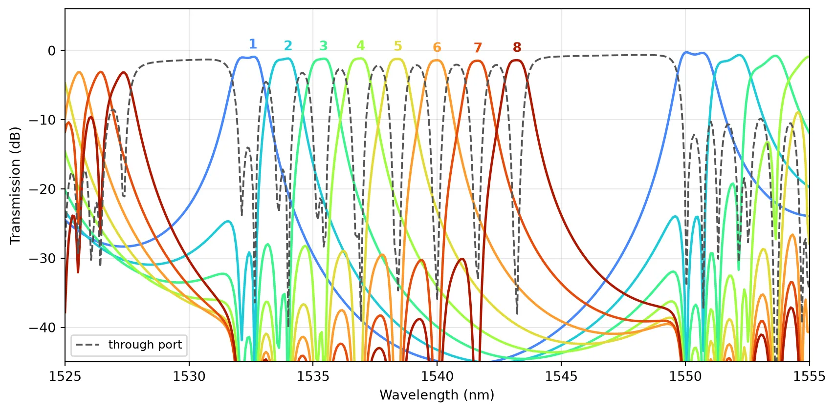
The numbers a link designer asks for are the channel spacing, the passband width, the drop loss, and how much of a neighbouring channel arrives at the wrong port.
for k in range(8): channel_db = 10 * np.log10(np.maximum(drops[k], 1e-12)) # Peak of this channel, and what every other channel delivers at that same wavelength. i = np.where(in_band)[0][np.argmax(channel_db[in_band])] others = {j: 10 * np.log10(max(drops[j][i], 1e-12)) for j in range(8) if j != k} adjacent = [others[j] for j in (k - 1, k + 1) if j in others] distant = [v for j, v in others.items() if j not in (k - 1, k + 1)] # 3 dB passband, restricted to the neighbourhood of the peak. band = np.where((channel_db > channel_db[i] - 3) & (np.abs(lam_chip - lam_chip[i]) < 3.0))[0] print(f"OUT{k + 1}: peak {channel_db[i]:5.2f} dB at {lam_chip[i]:7.2f} nm, " f"3 dB width {lam_chip[band.max()] - lam_chip[band.min()]:.2f} nm, " f"adjacent crosstalk {max(adjacent):6.1f} dB, non-adjacent {max(distant):6.1f} dB")OUT1: peak -0.91 dB at 1532.58 nm, 3 dB width 1.12 nm, adjacent crosstalk -33.5 dB, non-adjacent -46.9 dBOUT2: peak -1.15 dB at 1534.00 nm, 3 dB width 0.98 nm, adjacent crosstalk -20.8 dB, non-adjacent -68.5 dBOUT3: peak -1.18 dB at 1535.42 nm, 3 dB width 0.97 nm, adjacent crosstalk -21.8 dB, non-adjacent -32.2 dBOUT4: peak -1.14 dB at 1536.92 nm, 3 dB width 0.82 nm, adjacent crosstalk -22.5 dB, non-adjacent -33.4 dBOUT5: peak -1.22 dB at 1538.42 nm, 3 dB width 0.83 nm, adjacent crosstalk -22.8 dB, non-adjacent -33.8 dBOUT6: peak -1.40 dB at 1540.00 nm, 3 dB width 0.82 nm, adjacent crosstalk -23.2 dB, non-adjacent -34.2 dBOUT7: peak -1.47 dB at 1541.65 nm, 3 dB width 0.83 nm, adjacent crosstalk -23.9 dB, non-adjacent -34.5 dBOUT8: peak -1.40 dB at 1543.22 nm, 3 dB width 0.82 nm, adjacent crosstalk -22.9 dB, non-adjacent -34.0 dBSummary
Section titled “Summary”The eight channels land between 1532.6 nm and 1543.2 nm on a 1.52 nm grid, on a routed block of mm. The only geometry parameter that differs between stages is the phase-section length , at about 0.04 nm of wavelength per nm of . The drop loss, passband width, and crosstalk of each channel are printed above.
Moving the comb to a different grid means re-running the three-point calibration and the eight channel cavities. The circuit assembly and the routing are unchanged. The free spectral range of about 18 nm is the limit on how wide a comb one cavity design can carry.
Two numbers in the design are set by the etch rather than by the optics. The corrugation period follows from phase matching between the forward TE₀ and backward TE₁ modes, and the coupling gap of the mode demultiplexer has to clear the sidewall flare, which on a 200 nm ridge at 60 degrees removes 116 nm from each side of any gap drawn on the mask.
The same chip also works in reverse. Driving the OUT ports instead of IN multiplexes eight
sources onto one waveguide, since every component in the path is reciprocal.