

Electro-Optic Mach-Zehnder Modulator
In this notebook, we will design an electro-optic modulator based on the Pockels effect in a thin-film lithium niobate (TFLN) platform. The design is based on the work of Ying Li et al. [1], but using the open source LNOI400 PDK from Luxtelligence. Since the underlying technology differs, we do not expect to exactly reproduce the results reported in this work. However, the simulation results are in very good agreement with the foundry measurement, yielding VπL = 3.4 V.cm.
We will start with the calculation of VπL based on the optical waveguide and transmission line cross-sections defined in the PDK technology. Next, we can verify the modulation response and signal integrity of our design, and, finally, layout the full chip with coupling and reference structures.
References
- Ying Li, et al., “High-Performance Mach–Zehnder Modulator Based on Thin-Film Lithium Niobate with Low Voltage-Length Product,” ACS Omega 2023 8 (10), 9644-9651, doi: 10.1021/acsomega.3c00310.
import luxtelligence_lnoi400_forge as lxtimport numpy as npimport photonforge as pfimport tidy3d as tdfrom matplotlib import pyplot as plt
td.config.logging.level = "ERROR"
14:29:58 -03 WARNING: The material-library variant 'Palik_Lossless' is deprecated and maps to 'Palik_LowLoss' because it contains a tiny fitted loss despite its name. Use 'Palik_NoLoss' where available for a zero-loss Palik model.
Design of VπL
Section titled “Design of VπL”We compute the value of VπL for the modulator we want to design to define how long we will need it to be, based on the drivers we have available.
VπL can be derived exclusively by the optical waveguide and transmission line cross-section before the actual layout. This helps us define those cross-sections and make any required changes to the technology parameters and port specifications, if necessary.
Of course, for the VπL calculation, we need to account for the electrical field interaction with the substrate, so we include it in this first step.
tech = lxt.lnoi400()pf.config.default_technology = techOptical Waveguide
Section titled “Optical Waveguide”We can start by taking a look at the optical waveguide we will use. It is a wide multimode rib that is used for phase shifters and electro-optic modulators to reduce optical losses.
lda = 1.55wg_spec = tech.ports["RWG3000"]
_ = pf.tidy3d_plot(wg_spec, frequency=pf.C_0 / lda)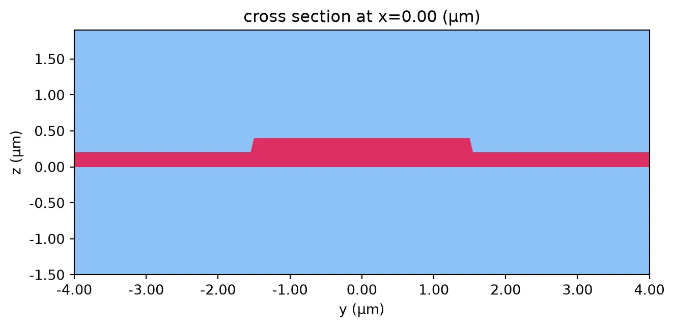
opt_solver = pf.port_modes(wg_spec, [pf.C_0 / lda], group_index=True)
_ = opt_solver.plot_field("E", "abs^2", mode_index=0)
opt_solver.data.to_dataframe()
Uploading task 'Mode-ModeSolver…'Starting task 'Mode-ModeSolver': https://tidy3d.simulation.cloud/workbench?taskId=mo-b23c64d8-c7d5-478c-956a-f8b2713da76cDownloading data from 'Mode-ModeSolver'…| wavelength | n eff | k eff | loss (dB/cm) | TE (Ey) fraction | wg TE fraction | wg TM fraction | mode area | group index | dispersion (ps/(nm km)) | ||
|---|---|---|---|---|---|---|---|---|---|---|---|
| f | mode_index | ||||||||||
| 1.934145e+14 | 0 | 1.55 | 1.848093 | 0.0 | 0.0 | 0.999712 | 0.988363 | 0.869788 | 1.397053 | 2.176146 | -438.086484 |
| 1 | 1.55 | 1.810298 | 0.0 | 0.0 | 0.997919 | 0.955418 | 0.874561 | 1.539675 | 2.208322 | -360.454085 | |
| 2 | 1.55 | 1.762410 | 0.0 | 0.0 | 0.004833 | 0.775415 | 0.987713 | 2.168234 | 2.295699 | -1326.498719 | |
| 3 | 1.55 | 1.749761 | 0.0 | 0.0 | 0.974982 | 0.908843 | 0.882403 | 1.850427 | 2.249283 | -456.187057 | |
| 4 | 1.55 | 1.721755 | 0.0 | 0.0 | 0.033712 | 0.785720 | 0.951274 | 2.261228 | 2.325592 | -1326.216054 |
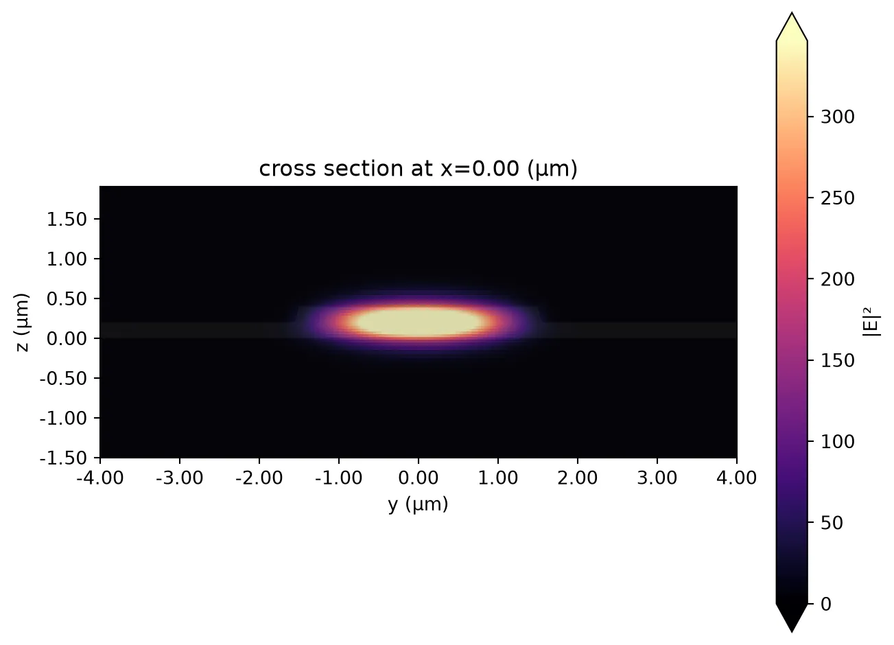
We see that this waveguide supports many modes, but we’re interested in the TE-like fundamental model (with mode_index == 0) with an effective index of 1.85 and group index of 2.20.
The design of a high-bandwidth electro-optic modulator with a low driving voltage requires careful simulation and a thorough understanding of the associated trade-offs. One critical factor is velocity matching between RF and optical signals. To achieve this, the RF transmission lines must be engineered so that the co-propagating optical and electrical signals travel at similar speeds (RF phase velocity close to the optical group velocity).
Another key consideration is the electrode geometry: narrower electrode gaps are necessary to generate a stronger electric field in the waveguide region, thereby enhancing the electro-optic modulation efficiency. However, the transmission line impedance must closely match the source impedance (typically 50 Ohms) to ensure efficient delivery of electrical signals with minimal losses. Achieving an optimized design typically involves iterating on the electrode geometry, optical etch depths, and the thicknesses and materials of the layer stack.
Coplanar Waveguide
Section titled “Coplanar Waveguide”Next, we will take a closer look at the RF transmission line cross-section we will be using.
We start with a simple transmission line without the waveguide in between the metal gap. The transmission line is a co-planar waveguide (CPW) geometry with 10 μm wide signal, 4 μm wide gap, and 180 μm wide ground line from the Foundry PDK itself.
# Define RF frequency range from 1 GHz to 65 GHzrf_freqs = np.linspace(1e9, 65e9, 20)
cpw_spec = tech.ports["UniCPW-EO"]ax = pf.tidy3d_plot(cpw_spec, frequency=rf_freqs[0])
ic = cpw_spec.to_tidy3d_impedance_calculator()_ = ic.voltage_integral.plot(ax=ax, x=0)_ = ic.current_integral.plot(ax=ax, x=0)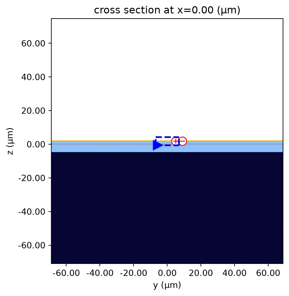
Analogously to the optical waveguide, we can easily calculate the CPW mode:
cpw_solver, z0 = pf.port_modes(cpw_spec, rf_freqs, impedance=True)
fig, ax = plt.subplots(1, 2, figsize=(9, 3), tight_layout=True)
cpw_solver.plot_field("Ey", "real", f=rf_freqs[0].item(), robust=False, ax=ax[0])
ax[1].plot(z0.f * 1e-9, z0.real)_ = ax[1].set(xlabel="Frequencies (GHz)", ylabel="Re{Z₀} (Ω)")
Uploading task 'Mode-ModeSolver…'Starting task 'Mode-ModeSolver': https://tidy3d.simulation.cloud/workbench?taskId=mo-a9e4c027-b612-4532-93f4-eec13ddd24d6Downloading data from 'Mode-ModeSolver'…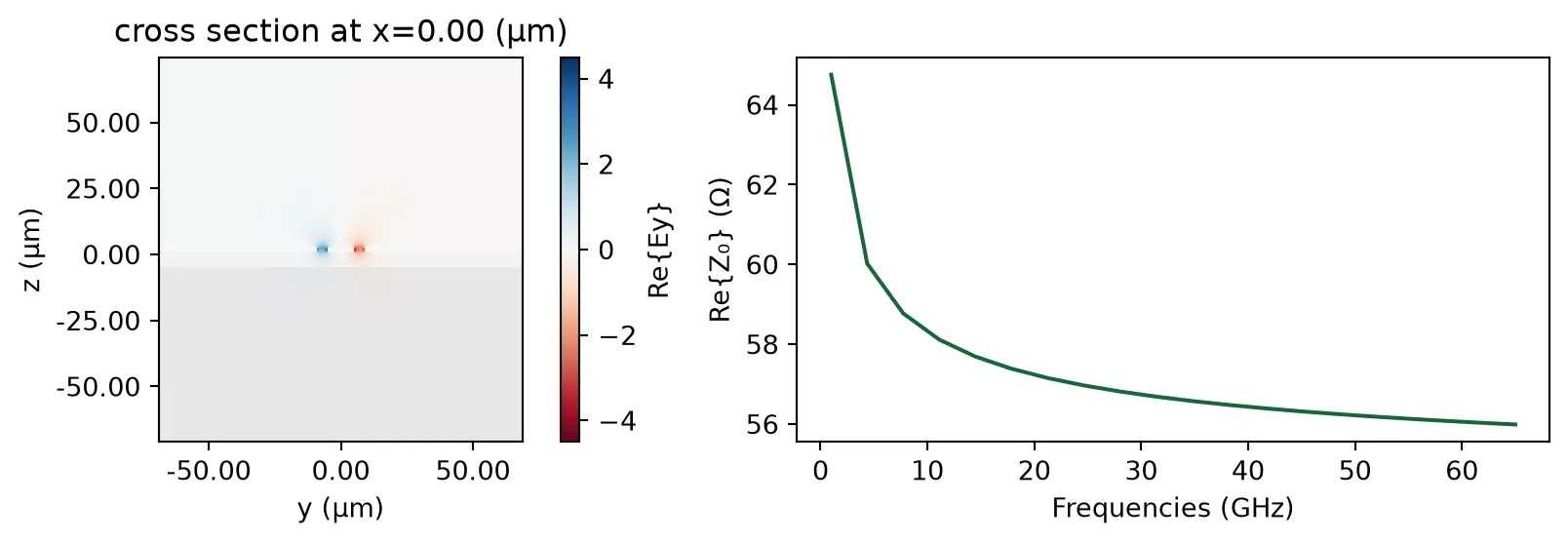
Computation of Vπ·L
Section titled “Computation of Vπ·L”PhotonForge allows us to combine both waveguide cross-sections to evaluate how effectively we can use the Pockels effect in this geometry to induce a phase shift in the MZM arm from the applied voltage. By running RF and optical simulations directly with all cross-perturbations included, PhotonForge allows designers to explore various trade-offs encountered when trying to design a high-bandwidth modulator with a low driving voltage.
We look at the path profiles of the CPW to get the gap and offset from the conductors:
cpw_paths = cpw_spec.path_profilescpw_paths{'gnd0': (180.0, -99.0, (21, 0)), 'gnd1': (180.0, 99.0, (21, 0)), 'signal': (10.0, 0.0, (21, 0))}ground_width, ground_offset, _ = cpw_paths["gnd1"]signal_width, _, _ = cpw_paths["signal"]offset = (ground_offset - ground_width / 2 + signal_width / 2) / 2gap = ground_offset - ground_width / 2 - signal_width / 2
print(f"Offset: {offset} μm\nGap: {gap} μm")Offset: 7.0 μmGap: 4.0 μmNow we combine the CPW with 2 optical waveguide profiles at the appropriate offsets:
mzm_spec = cpw_spec.combined_with(wg_spec, offset).combined_with(wg_spec, -offset)
ax = pf.tidy3d_plot(mzm_spec, frequency=rf_freqs[0])ic.voltage_integral.plot(ax=ax, x=0)_ = ic.current_integral.plot(ax=ax, x=0)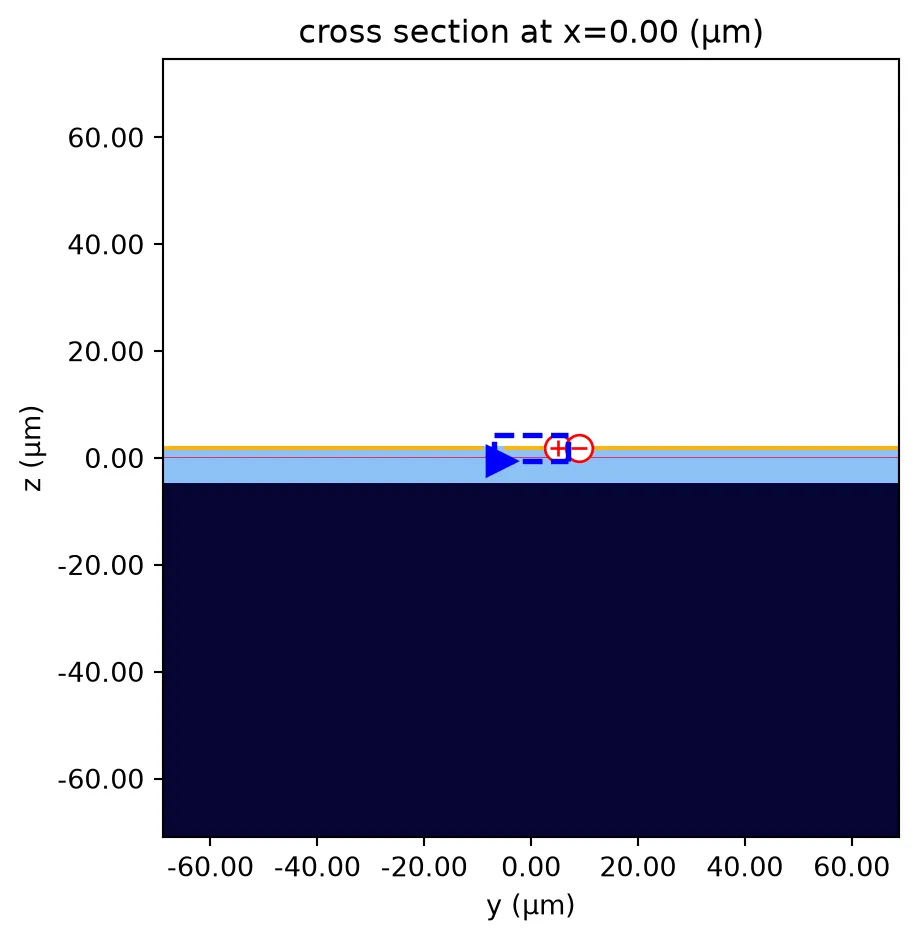
We solve again for the electric field profile, but we add mesh override structures to make sure the RF field is finely resolved in the optical waveguide region. To do so, we manually export the mode solver and update it with the desired overrides.
# Get the minimal grid spacing from the optical simulation to use here as welldy = np.diff(opt_solver.simulation.grid.boundaries.z).min()dz = np.diff(opt_solver.simulation.grid.boundaries.z).min()
# Mesh override parametersdl = (None, dy, dz)ln_thickness = tech.parametric_kwargs["ln_thickness"]size = (td.inf, gap, ln_thickness)
mzm_solver = mzm_spec.to_tidy3d(frequencies=rf_freqs, mesh_refinement=25)mzm_solver = mzm_solver.updated_copy(    "simulation/grid_spec",    override_structures=[        td.MeshOverrideStructure(            geometry=td.Box(center=(0, -offset, ln_thickness / 2), size=size), dl=dl        ),        td.MeshOverrideStructure(            geometry=td.Box(center=(0, offset, ln_thickness / 2), size=size), dl=dl        ),    ],)ax = mzm_solver.plot()mzm_solver.plot_grid(ax=ax)_ = ax.set(xlim=(offset - 4, offset + 4), ylim=(-1, 3))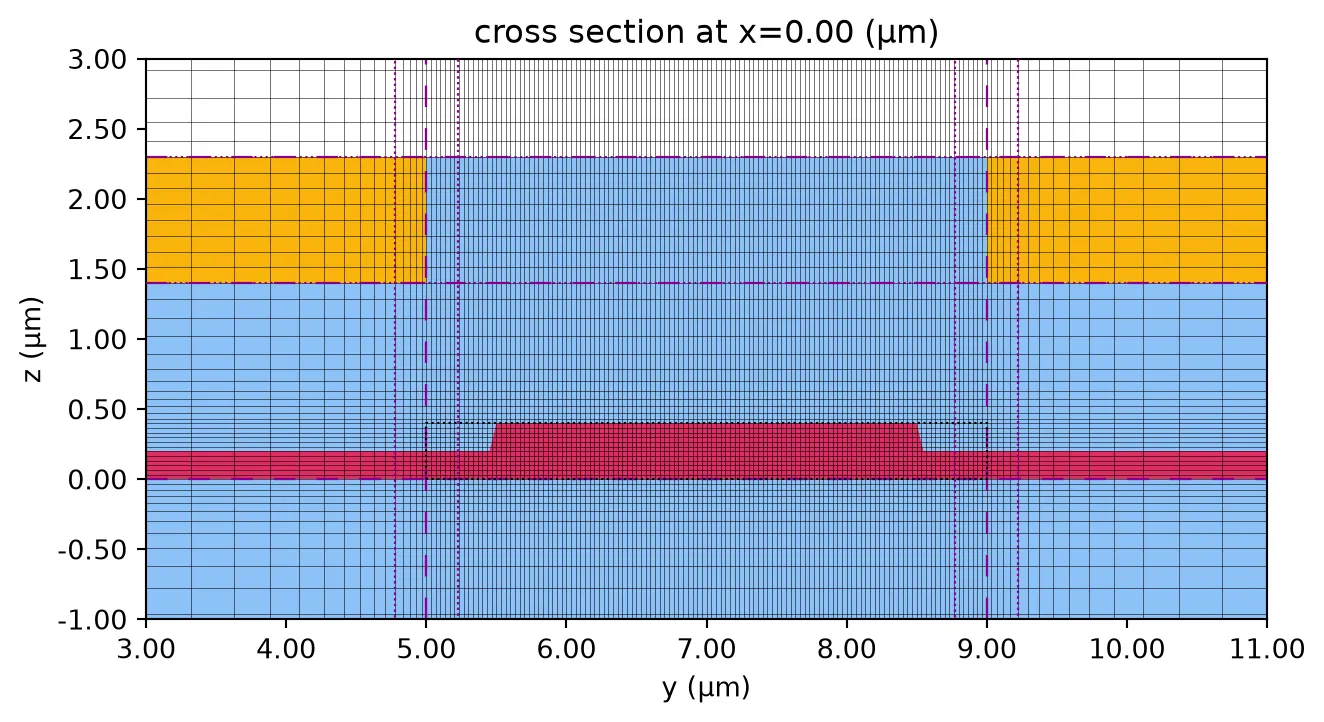
In the field plot we can clearly see the effects of the dielectric waveguides. We care about the Ey field component (the one aligned to z crystal axis in the X-cut LiNbO₃), because this field results in index change along z crystal axis due to large electro-optic coefficient ().
mzm_solver = pf.port_modes(mzm_solver)
_ = mzm_solver.plot_field("Ey", "real", f=rf_freqs[0].item(), robust=True)
Uploading task 'Mode-ModeSolver…'Starting task 'Mode-ModeSolver': https://tidy3d.simulation.cloud/workbench?taskId=mo-68c091b8-d56b-408f-a4c6-683f8758fbf0Downloading data from 'Mode-ModeSolver'…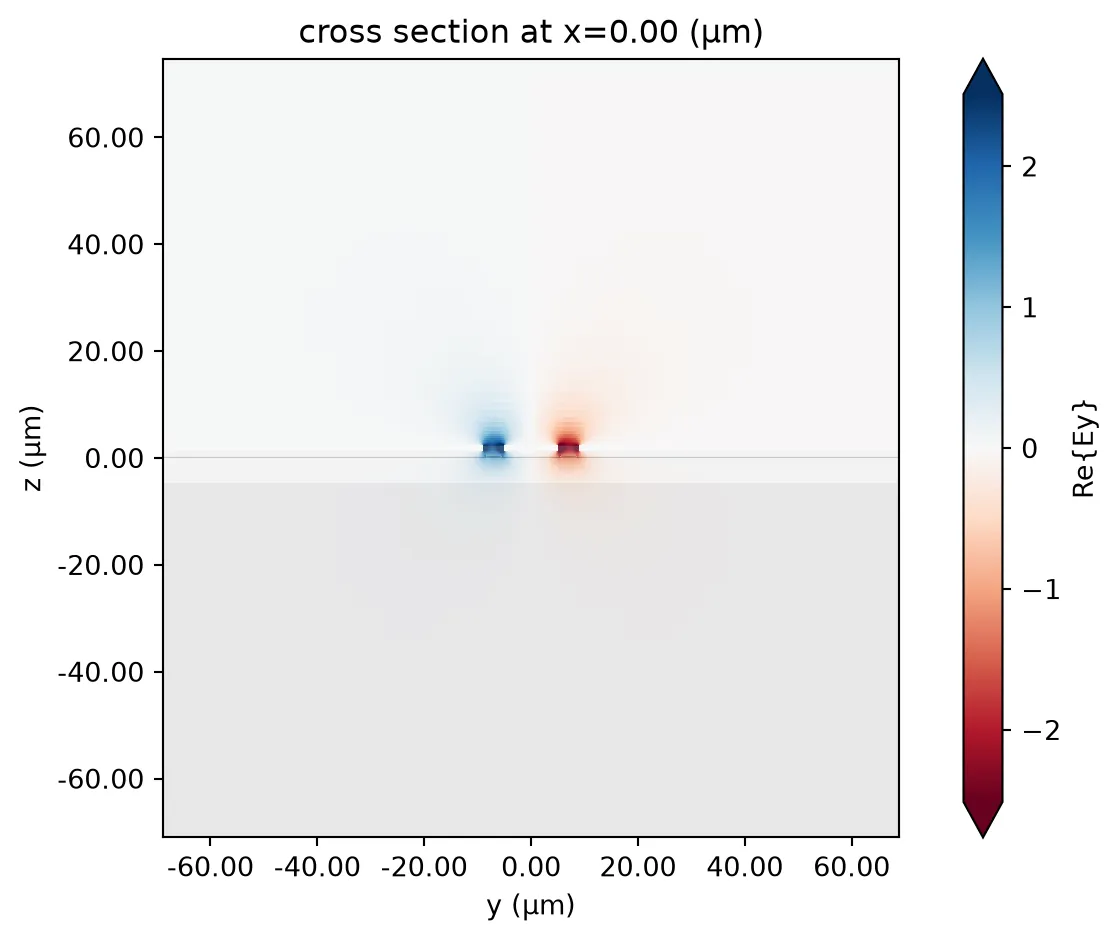
We are also interested in the characteristics for the MZM cross-section, readily available from the mode solver data and the impedance calculator from before.
Note that we cannot use the argument impedance=True in port_modes because we are passing a Tidy3D mode solver to it, not a port or port specification, and the mode solver does not contain the required information to calculate the impedance.
n_eff = mzm_solver.data.n_eff.isel(mode_index=0).valuesz0 = ic.compute_impedance(mzm_solver.data)
fig, ax = plt.subplots(1, 2, figsize=(8, 3), tight_layout=True)
ax[0].plot(rf_freqs * 1e-9, n_eff, ".-")ax[0].set(ylabel="Effective Index", xlabel="Frequency (GHz)")
ax[1].plot(rf_freqs * 1e-9, np.real(z0), ".-")_ = ax[1].set(ylabel="Re{Z₀} (Ω)", xlabel="Frequency (GHz)")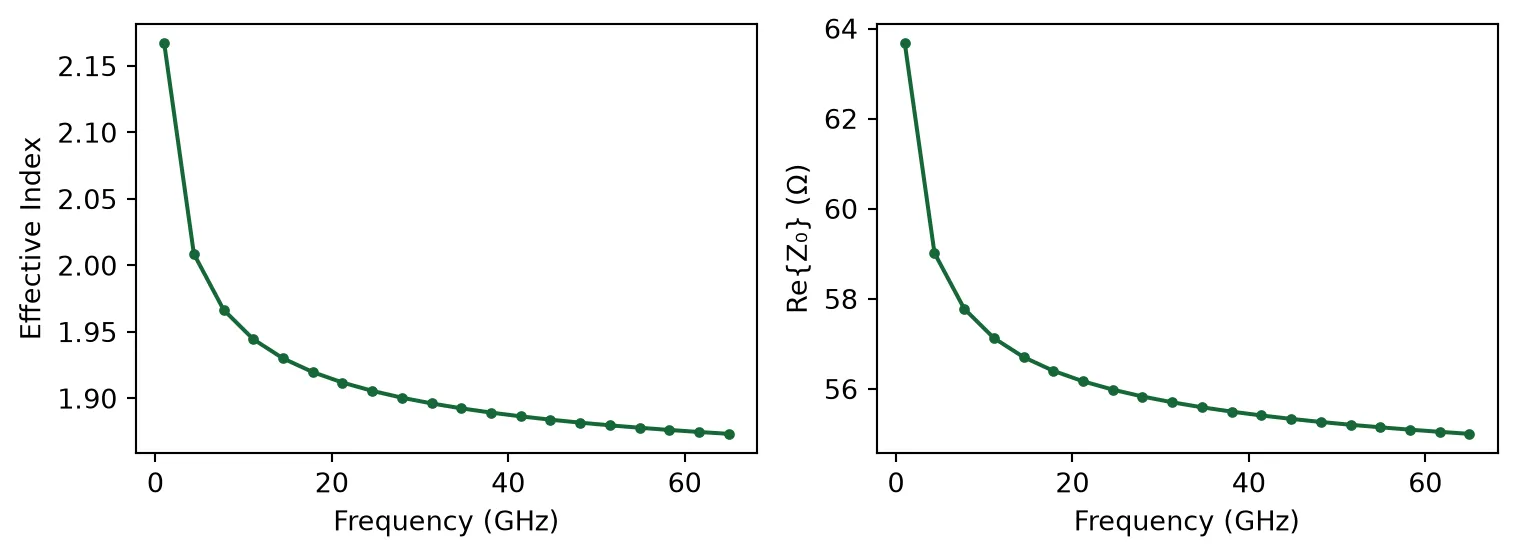
These results match closely the experimental data measured by the foundry at 65 GHZ: effective index around 1.88 and characteristic impedance of 55.6 Ω.
We will use the electrical field in the direction of the LiNbO₃ cut in this platform to perturb the optical medium. To do so, we first need to normalize the field by the voltage and offset its coordinates to match the optical simulation, where the dielectric waveguide is centered around y=0.
v0 = ic.voltage_integral.compute_voltage(mzm_solver.data)
ey_norm = (mzm_solver.data.Ey / v0).isel(f=0, mode_index=0, drop=True).absey_norm = ey_norm.assign_coords(y=ey_norm.y - offset)
ey_norm.isel(x=0).transpose("z", "y").plot(robust=True)# _ = plt.gca().set(xlim=(-gap, gap), ylim=(-1, 4))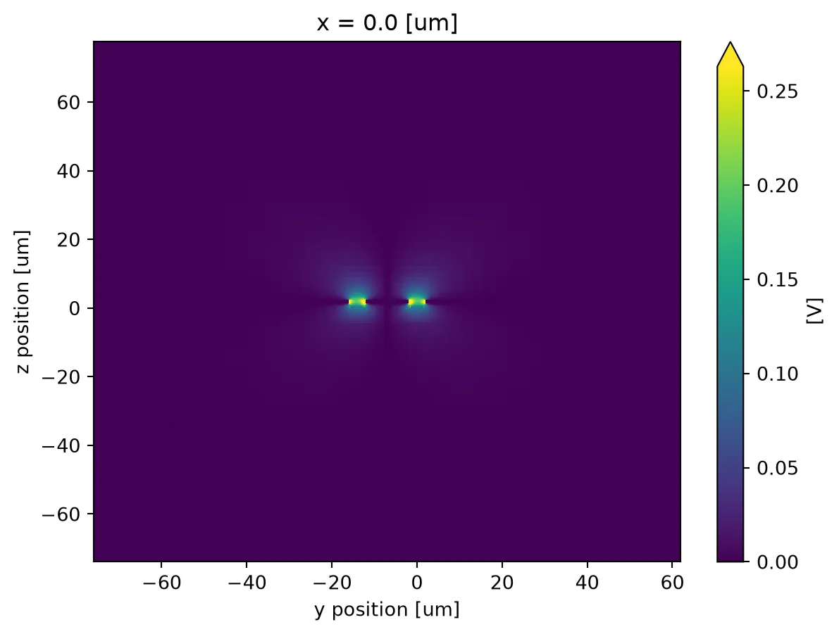
The normalized electrical field is used to perturb the LiNbO₃ in the z axis of the crystal according to the Pockels effect model:
ln = td.material_library["LiNbO3"]["Zelmon1997"](optical_axis=1)eps_o, eps_e, _ = (e.real for e in ln.eps_diagonal(pf.C_0 / lda))
n_e = eps_e**0.5r33 = 30.9e-6  # μm/V
# Index variation derived from the RF fieldΔn = -0.5 * n_e**3 * r33 * ey_norm
# We plot the whole domain, but the perturbation will only take effect over the LiNbO₃, not everywhere_ = Δn.isel(x=0).transpose("z", "y").plot(robust=False)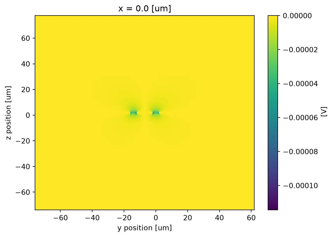
We can create a small function that generates the perturbed medium depending on the voltage and calculates the modes. The perturbed medium is created as a custom anisotropic medium from Tidy3D:
# Use a single data point for the homogeneous directionseps_o_array = td.SpatialDataArray(    np.full((1, 1, 1), eps_o), coords={"x": [0], "y": [0], "z": [0]})
def perturbed_solver(voltage):    perturbed_ln = td.CustomAnisotropicMedium(        xx=td.CustomMedium(permittivity=eps_o_array, subpixel=True),        yy=td.CustomMedium(permittivity=(n_e + voltage * Δn) ** 2, subpixel=True),        zz=td.CustomMedium(permittivity=eps_o_array, subpixel=True),    )    # We use the same optical waveguide as before and change the LiNbO₃ medium in the technology    return pf.port_modes(        wg_spec, [pf.C_0 / lda], technology=lxt.lnoi400(ln=perturbed_ln)    )
We calculate the effective index for a few voltage values to derive Vπ·L:
voltages = np.arange(5)n_eff = [    perturbed_solver(v).data.n_eff.isel(mode_index=0, f=0).item() for v in voltages]
_ = plt.plot(voltages, n_eff, ".-")plt.gca().set(xlabel="Voltage (V)", ylabel="Optical Effective Index")
# The variation is quite linear, so we simply use the largest intervaldneff_dV = abs(n_eff[-1] - n_eff[0]) / (voltages[-1] - voltages[0])
vpil = 0.5 * lda / dneff_dV  # in V·μm"
print(f"Vπ·L (single-drive) = {vpil * 1e-4:.2f} V·cm")print(f"Vπ·L (push-pull)    = {vpil * 1e-4 / 2:.2f} V·cm")
Uploading task 'Mode-ModeSolver…'Starting task 'Mode-ModeSolver': https://tidy3d.simulation.cloud/workbench?taskId=mo-a3008079-2a6b-4c5d-8996-e37efcebe3c9Downloading data from 'Mode-ModeSolver'…Uploading task 'Mode-ModeSolver…'Starting task 'Mode-ModeSolver': https://tidy3d.simulation.cloud/workbench?taskId=mo-81c26895-e0b4-4035-a347-44d128a19c88Downloading data from 'Mode-ModeSolver'…Uploading task 'Mode-ModeSolver…'Starting task 'Mode-ModeSolver': https://tidy3d.simulation.cloud/workbench?taskId=mo-7ad9e3f4-ddd6-473e-8060-24ce31a67771Downloading data from 'Mode-ModeSolver'…Uploading task 'Mode-ModeSolver…'Starting task 'Mode-ModeSolver': https://tidy3d.simulation.cloud/workbench?taskId=mo-2e794e2e-2f80-46f5-a7b1-0b83b4e2006bDownloading data from 'Mode-ModeSolver'…Uploading task 'Mode-ModeSolver…'Starting task 'Mode-ModeSolver': https://tidy3d.simulation.cloud/workbench?taskId=mo-deb25b58-7c90-4755-aa61-3775da5bf8ddDownloading data from 'Mode-ModeSolver'…Vπ·L (single-drive) = 5.48 V·cmVπ·L (push-pull) = 2.74 V·cm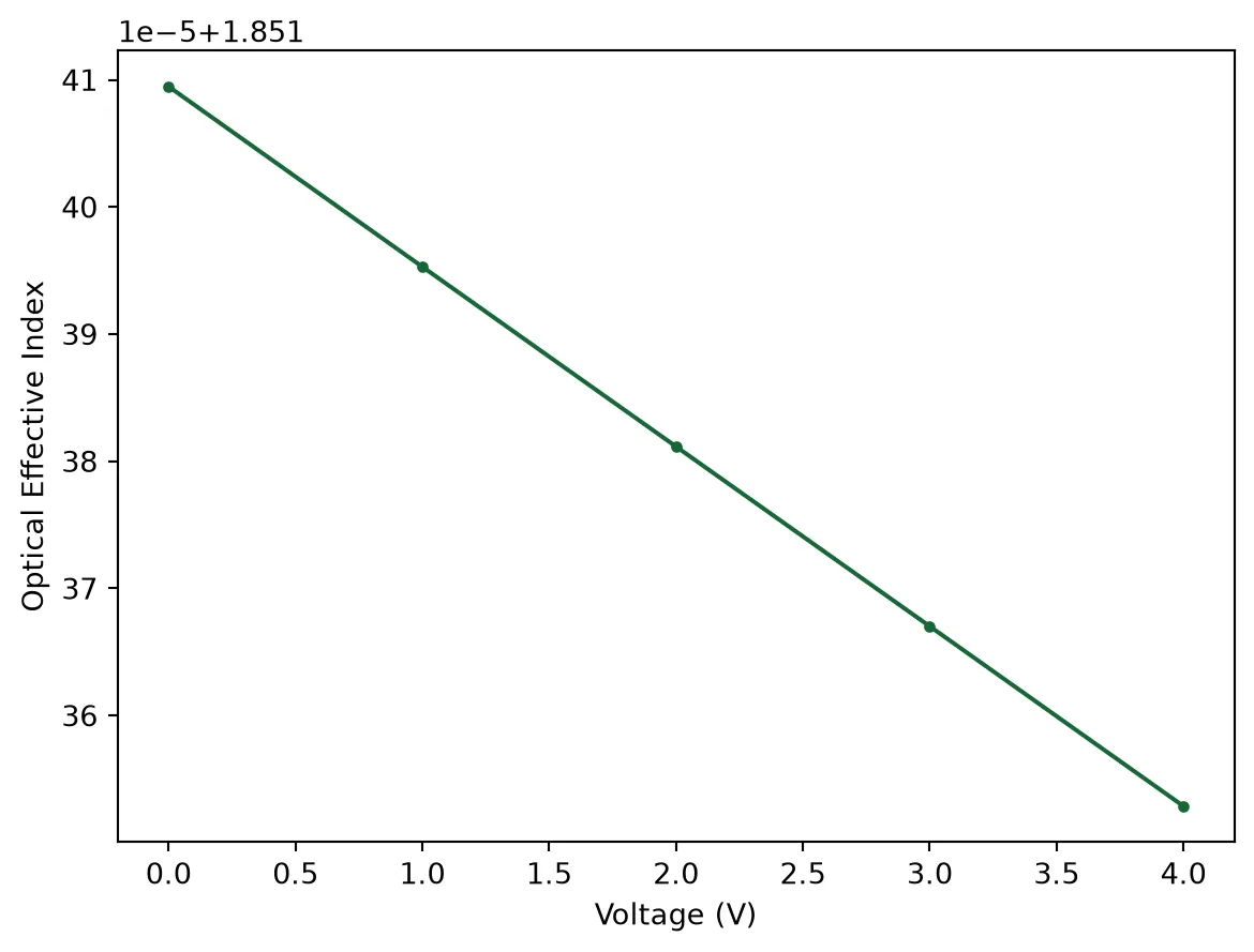
Finally, we can also include the penalty for impedance mismatch and voltage scaling to Vπ·L:
z_load = 50  # Ωz0_low_freq = z0.isel(f=0).real.item()
vpil_mismatch = vpil * (2 * z0_low_freq) / (z0_low_freq + z_load)
print(f"Mismatched Vπ·L (single-drive) = {vpil_mismatch * 1e-4:.2f} V·cm")print(f"Mismatched Vπ·L (push-pull)    = {vpil_mismatch * 1e-4 / 2:.2f} V·cm")
Mismatched Vπ·L (single-drive) = 6.14 V·cmMismatched Vπ·L (push-pull) = 3.07 V·cmChip Layout
Section titled “Chip Layout”After the initial design, we can create the full Mach-Zehnder modulator chip layout.
# Single mode waveguide as defaultrouting_spec = tech.ports["RWG1000"]pf.config.default_kwargs = {"radius": 70, "port_spec": routing_spec}
freqs = td.frequencies.c_band()
from photonforge.live_viewer import LiveViewer
viewer = LiveViewer()LiveViewer started at http://127.0.0.1:44545. Call its 'stop()' method to free the port.Mach-Zehnder Arms
Section titled “Mach-Zehnder Arms”The CPW will need to be contacted on both ends using GSG (ground-signal-ground) pads. They can be created from electrical terminals:
@pf.parametric_component()def gsg_pad(*, pad_size=(100, 100), pad_gap=50):    c = pf.Component()    c.add_terminal(        pf.Terminal(            "TL", pf.Rectangle(center=(0, -pad_size[1] - pad_gap), size=pad_size)        ),        "G0",    )    c.add_terminal(pf.Terminal("TL", pf.Rectangle(center=(0, 0), size=pad_size)), "S")    c.add_terminal(        pf.Terminal(            "TL", pf.Rectangle(center=(0, pad_size[1] + pad_gap), size=pad_size)        ),        "G1",    )    return c
pad = gsg_pad()viewer(pad)
The MZM arms are built from parametric straight sections, and the pads are routed using tapers to the CPW terminals:
@pf.parametric_component()def mzm_arms(*, length=3000, taper_length=150):    c = pf.Component()
    tline = c.add_reference(pf.parametric.straight(port_spec=cpw_spec, length=length))
    cpw_paths = cpw_spec.path_profiles    width_gnd, offset_gnd, _ = cpw_paths["gnd1"]    width_sig, _, _ = cpw_paths["signal"]    offset = (offset_gnd - width_gnd / 2 + width_sig / 2) / 2
    opt_wg = pf.parametric.straight(length=length, port_spec=wg_spec)    bot_arm = c.add_reference(opt_wg).translate((0, -offset))    top_arm = c.add_reference(opt_wg).translate((0, offset))
    c.add_port([bot_arm["P0"], top_arm["P0"], bot_arm["P1"], top_arm["P1"]])
    pad0 = c.add_reference(pad)    pad1 = c.add_reference(pad)    pad0.x_max = tline.x_min - taper_length    pad1.x_min = tline.x_max + taper_length
    c.add_terminal(        {            f"{name}:{suffix}": pad[name]            for pad, suffix in [(pad0, "in"), (pad1, "out")]            for name in ("G0", "G1", "S")        }    )
    c.add(        pf.parametric.route_taper(            terminal1=pad0["G0"], terminal2=tline["E0"].terminals("gnd0")        ),        pf.parametric.route_taper(            terminal1=pad0["S"], terminal2=tline["E0"].terminals("signal")        ),        pf.parametric.route_taper(            terminal1=pad0["G1"], terminal2=tline["E0"].terminals("gnd1")        ),        pf.parametric.route_taper(            terminal1=pad1["G0"], terminal2=tline["E1"].terminals("gnd0")        ),        pf.parametric.route_taper(            terminal1=pad1["S"], terminal2=tline["E1"].terminals("signal")        ),        pf.parametric.route_taper(            terminal1=pad1["G1"], terminal2=tline["E1"].terminals("gnd1")        ),    )
    return c
arms = mzm_arms()viewer(arms);fill:%23221f20;font-weight:bold;font-size:29.600000px;}.terminal{fill:none;stroke:%23805080;stroke-width:3.700000;}.dashed{stroke-dasharray:18.500000,11.100000;}.port{fill:none;stroke:%23805080;stroke-width:7.400000;}.virtual-connection{fill:none;stroke:%23907090;stroke-width:5.550000;}.layer_31_0{stroke:%23d4467c;fill:url(%23pat-layer_31_0);fill-opacity:0.492;}.label_31_0{fill:%23d4467c;}.layer_6_0{stroke:%237c605a;fill:url(%23pat-layer_6_0);fill-opacity:0.492;}.label_6_0{fill:%237c605a;}.layer_6_1{stroke:%2300d080;fill:url(%23pat-layer_6_1);fill-opacity:0.492;}.label_6_1{fill:%2300d080;}.layer_201_0{stroke:%23857b75;fill:url(%23pat-layer_201_0);fill-opacity:0.492;}.label_201_0{fill:%23857b75;}.layer_50_1{stroke:%23c7031c;fill:url(%23pat-layer_50_1);fill-opacity:0.492;}.label_50_1{fill:%23c7031c;}.layer_21_1{stroke:%233503fc;fill:url(%23pat-layer_21_1);fill-opacity:0.492;}.label_21_1{fill:%233503fc;}.layer_4_0{stroke:%235179b5;fill:url(%23pat-layer_4_0);fill-opacity:0.492;}.label_4_0{fill:%235179b5;}.layer_2_0{stroke:%237d57de;fill:url(%23pat-layer_2_0);fill-opacity:0.492;}.label_2_0{fill:%237d57de;}.layer_3_0{stroke:%23000080;fill:url(%23pat-layer_3_0);fill-opacity:0.492;}.label_3_0{fill:%23000080;}.layer_2_1{stroke:%23ff00ff;fill:url(%23pat-layer_2_1);fill-opacity:0.492;}.label_2_1{fill:%23ff00ff;}.layer_3_1{stroke:%236750bf;fill:url(%23pat-layer_3_1);fill-opacity:0.492;}.label_3_1{fill:%236750bf;}.layer_21_0{stroke:%233503fc;fill:url(%23pat-layer_21_0);fill-opacity:0.492;}.label_21_0{fill:%233503fc;}.layer_990_0{stroke:%23473328;fill:none;}.label_990_0{fill:%23473328;}</style><defs><path id=%22port-symbol%22 class=%22port%22 d=%22M 0,-14.800000 L 22.200000,0 0,14.800000%22 /><path id=%22ref-port-symbol%22 class=%22port%22 style=%22stroke-opacity:0.33;%22 d=%22M 0,-11.100000 C 14.800000,-11.100000 14.800000,11.100000 0,11.100000%22 /><circle id=%22port-bend-symbol%22 style=%22stroke-width:0;stroke:none;fill:%23805080;fill-opacity:1;%22 cx=%220%22 cy=%220%22 r=%226.660000%22 /><circle id=%22connection-symbol%22 style=%22stroke-width:0;stroke:none;fill:%23907090;fill-opacity:1;%22 cx=%220%22 cy=%220%22 r=%227.770000%22 /><pattern id=%22pat-layer_31_0%22 patternUnits=%22userSpaceOnUse%22 width=%2211.100000%22 height=%2211.100000%22 patternTransform=%22translate(8.488235,10.515789)%22><circle cx=%225.550000%22 cy=%225.550000%22 r=%221.850000%22 style=%22stroke:none;fill:%23d4467c;fill-opacity:1.0%22 /></pattern><pattern id=%22pat-layer_6_0%22 patternUnits=%22userSpaceOnUse%22 width=%2218.500000%22 height=%2218.500000%22 patternTransform=%22translate(8.705882,8.763158)%22><line x1=%220%22 y1=%229.250000%22 x2=%2218.500000%22 y2=%229.250000%22 style=%22stroke:%237c605a;stroke-width:1.850000%22 /></pattern><pattern id=%22pat-layer_6_1%22 patternUnits=%22userSpaceOnUse%22 width=%2211.100000%22 height=%2211.100000%22 patternTransform=%22translate(2.611765,7.010526)%22><line x1=%225.550000%22 y1=%220%22 x2=%225.550000%22 y2=%2211.100000%22 style=%22stroke:%2300d080;stroke-width:1.850000%22 /></pattern><pattern id=%22pat-layer_201_0%22 patternUnits=%22userSpaceOnUse%22 width=%2211.100000%22 height=%2211.100000%22 patternTransform=%22translate(8.488235,4.089474)%22><line x1=%225.550000%22 y1=%220%22 x2=%225.550000%22 y2=%2211.100000%22 style=%22stroke:%23857b75;stroke-width:1.850000%22 /><line x1=%220%22 y1=%225.550000%22 x2=%2211.100000%22 y2=%225.550000%22 style=%22stroke:%23857b75;stroke-width:1.850000%22 /></pattern><pattern id=%22pat-layer_50_1%22 patternUnits=%22userSpaceOnUse%22 width=%2211.100000%22 height=%2211.100000%22 patternTransform=%22translate(3.917647,1.168421)%22><line x1=%220%22 y1=%220%22 x2=%2211.100000%22 y2=%2211.100000%22 style=%22stroke:%23c7031c;stroke-width:1.850000%22 /><line x1=%22-5.550000%22 y1=%225.550000%22 x2=%225.550000%22 y2=%2216.650000%22 style=%22stroke:%23c7031c;stroke-width:1.850000%22 /><line x1=%225.550000%22 y1=%22-5.550000%22 x2=%2216.650000%22 y2=%225.550000%22 style=%22stroke:%23c7031c;stroke-width:1.850000%22 /><line x1=%2211.100000%22 y1=%220%22 x2=%220%22 y2=%2211.100000%22 style=%22stroke:%23c7031c;stroke-width:1.850000%22 /><line x1=%2216.650000%22 y1=%225.550000%22 x2=%225.550000%22 y2=%2216.650000%22 style=%22stroke:%23c7031c;stroke-width:1.850000%22 /><line x1=%225.550000%22 y1=%22-5.550000%22 x2=%22-5.550000%22 y2=%225.550000%22 style=%22stroke:%23c7031c;stroke-width:1.850000%22 /></pattern><pattern id=%22pat-layer_21_1%22 patternUnits=%22userSpaceOnUse%22 width=%2218.500000%22 height=%2218.500000%22 patternTransform=%22translate(7.617647,5.842105)%22><circle cx=%229.250000%22 cy=%229.250000%22 r=%221.850000%22 style=%22stroke:none;fill:%233503fc;fill-opacity:1.0%22 /></pattern><pattern id=%22pat-layer_4_0%22 patternUnits=%22userSpaceOnUse%22 width=%2218.500000%22 height=%2218.500000%22 patternTransform=%22translate(11.970588,5.842105)%22><line x1=%229.250000%22 y1=%220%22 x2=%229.250000%22 y2=%2218.500000%22 style=%22stroke:%235179b5;stroke-width:1.850000%22 /></pattern><pattern id=%22pat-layer_2_0%22 patternUnits=%22userSpaceOnUse%22 width=%2218.500000%22 height=%2218.500000%22 patternTransform=%22translate(15.235294,2.921053)%22><line x1=%220%22 y1=%220%22 x2=%2218.500000%22 y2=%2218.500000%22 style=%22stroke:%237d57de;stroke-width:1.850000%22 /><line x1=%22-9.250000%22 y1=%229.250000%22 x2=%229.250000%22 y2=%2227.750000%22 style=%22stroke:%237d57de;stroke-width:1.850000%22 /><line x1=%229.250000%22 y1=%22-9.250000%22 x2=%2227.750000%22 y2=%229.250000%22 style=%22stroke:%237d57de;stroke-width:1.850000%22 /></pattern><pattern id=%22pat-layer_3_0%22 patternUnits=%22userSpaceOnUse%22 width=%2211.100000%22 height=%2211.100000%22 patternTransform=%22translate(2.611765,8.178947)%22><line x1=%220%22 y1=%220%22 x2=%2211.100000%22 y2=%2211.100000%22 style=%22stroke:%23000080;stroke-width:1.850000%22 /><line x1=%22-5.550000%22 y1=%225.550000%22 x2=%225.550000%22 y2=%2216.650000%22 style=%22stroke:%23000080;stroke-width:1.850000%22 /><line x1=%225.550000%22 y1=%22-5.550000%22 x2=%2216.650000%22 y2=%225.550000%22 style=%22stroke:%23000080;stroke-width:1.850000%22 /></pattern><pattern id=%22pat-layer_2_1%22 patternUnits=%22userSpaceOnUse%22 width=%2211.100000%22 height=%2211.100000%22 patternTransform=%22translate(6.529412,3.505263)%22><line x1=%2211.100000%22 y1=%220%22 x2=%220%22 y2=%2211.100000%22 style=%22stroke:%23ff00ff;stroke-width:1.850000%22 /><line x1=%2216.650000%22 y1=%225.550000%22 x2=%225.550000%22 y2=%2216.650000%22 style=%22stroke:%23ff00ff;stroke-width:1.850000%22 /><line x1=%225.550000%22 y1=%22-5.550000%22 x2=%22-5.550000%22 y2=%225.550000%22 style=%22stroke:%23ff00ff;stroke-width:1.850000%22 /></pattern><pattern id=%22pat-layer_3_1%22 patternUnits=%22userSpaceOnUse%22 width=%2218.500000%22 height=%2218.500000%22 patternTransform=%22translate(0.000000,16.552632)%22><line x1=%220%22 y1=%220%22 x2=%2218.500000%22 y2=%2218.500000%22 style=%22stroke:%236750bf;stroke-width:1.850000%22 /><line x1=%22-9.250000%22 y1=%229.250000%22 x2=%229.250000%22 y2=%2227.750000%22 style=%22stroke:%236750bf;stroke-width:1.850000%22 /><line x1=%229.250000%22 y1=%22-9.250000%22 x2=%2227.750000%22 y2=%229.250000%22 style=%22stroke:%236750bf;stroke-width:1.850000%22 /></pattern><pattern id=%22pat-layer_21_0%22 patternUnits=%22userSpaceOnUse%22 width=%2211.100000%22 height=%2211.100000%22 patternTransform=%22translate(7.182353,1.752632)%22><line x1=%220%22 y1=%225.550000%22 x2=%2211.100000%22 y2=%225.550000%22 style=%22stroke:%233503fc;stroke-width:1.850000%22 /></pattern><g id=%22C1%22 data-name=%22straight__AG6SILVP37K2TEZZWX3AT24APB5V2ZFF2EQZCHJ7MFLQSWV5WG3Q%22><path class=%22layer_21_0%22 d=%22M 0.000000,-189.000000 3000.000000,-189.000000 3000.000000,-9.000000 0.000000,-9.000000 z%22 /><path class=%22layer_21_0%22 d=%22M 0.000000,9.000000 3000.000000,9.000000 3000.000000,189.000000 0.000000,189.000000 z%22 /><path class=%22layer_21_0%22 d=%22M 0.000000,-5.000000 3000.000000,-5.000000 3000.000000,5.000000 0.000000,5.000000 z%22 /></g><g id=%22C2%22 data-name=%22straight__COQUAEHJ3TMV6MSBWNCAOFHBICTW7SBMD3WQGXAUREJWA5HFT2EA%22><path class=%22layer_2_0%22 d=%22M 0.000000,-1.500000 3000.000000,-1.500000 3000.000000,1.500000 0.000000,1.500000 z%22 /><path class=%22layer_3_0%22 d=%22M 0.000000,-6.000000 3000.000000,-6.000000 3000.000000,6.000000 0.000000,6.000000 z%22 /></g><g id=%22C3%22 data-name=%22gsg_pad__EHZT4TPCDWNKDTN7XW5UFRPU6DHM2SJETLFKVCGZI6SCYBGCMJ3Q%22><rect class=%22terminal dashed%22 x=%22-50.000000%22 y=%22-200.000000%22 width=%22100.000000%22 height=%22100.000000%22 /><rect class=%22terminal dashed%22 x=%22-50.000000%22 y=%22100.000000%22 width=%22100.000000%22 height=%22100.000000%22 /><rect class=%22terminal dashed%22 x=%22-50.000000%22 y=%22-50.000000%22 width=%22100.000000%22 height=%22100.000000%22 /></g><g id=%22C4%22 data-name=%22route_taper__M2ROCEGOJLW3HT7CARRZUGQ6ZZVBXEDEJVO6TLBFOKEJ7GFKPSIQ%22><path class=%22layer_21_0%22 d=%22M -100.000000,-100.000000 -200.000000,-100.000000 -200.000000,-200.000000 -100.000000,-200.000000 0.000000,-189.000000 0.000000,-9.000000 z%22 /><rect class=%22terminal dashed%22 x=%22-200.000000%22 y=%22-200.000000%22 width=%22100.000000%22 height=%22100.000000%22 /><rect class=%22terminal dashed%22 x=%220.000000%22 y=%22-189.000000%22 width=%220.000000%22 height=%22180.000000%22 /></g><g id=%22C5%22 data-name=%22route_taper__3FI24T52I5STIIBAEYXOT3OJODLXCZ7ODECZUAQYWKMXI6YTFU6A%22><path class=%22layer_21_0%22 d=%22M -100.000000,50.000000 -200.000000,50.000000 -200.000000,-50.000000 -100.000000,-50.000000 0.000000,-5.000000 0.000000,5.000000 z%22 /><rect class=%22terminal dashed%22 x=%22-200.000000%22 y=%22-50.000000%22 width=%22100.000000%22 height=%22100.000000%22 /><rect class=%22terminal dashed%22 x=%220.000000%22 y=%22-5.000000%22 width=%220.000000%22 height=%2210.000000%22 /></g><g id=%22C6%22 data-name=%22route_taper__5KJBAW27FA63EAP3RJXMXB6SX3FDZNEIOSLYYKFBH7C6VIWWBXNA%22><path class=%22layer_21_0%22 d=%22M -100.000000,200.000000 -200.000000,200.000000 -200.000000,100.000000 -100.000000,100.000000 0.000000,9.000000 0.000000,189.000000 z%22 /><rect class=%22terminal dashed%22 x=%22-200.000000%22 y=%22100.000000%22 width=%22100.000000%22 height=%22100.000000%22 /><rect class=%22terminal dashed%22 x=%220.000000%22 y=%229.000000%22 width=%220.000000%22 height=%22180.000000%22 /></g><g id=%22C7%22 data-name=%22route_taper__WNDRC65BALYZPNB7XX3FEBC2UGZEKYKCY7M4VLNKXEHQN2GAF4DQ%22><path class=%22layer_21_0%22 d=%22M 3000.000000,-9.000000 3000.000000,-189.000000 3100.000000,-200.000000 3200.000000,-200.000000 3200.000000,-100.000000 3100.000000,-100.000000 z%22 /><rect class=%22terminal dashed%22 x=%223100.000000%22 y=%22-200.000000%22 width=%22100.000000%22 height=%22100.000000%22 /><rect class=%22terminal dashed%22 x=%223000.000000%22 y=%22-189.000000%22 width=%220.000000%22 height=%22180.000000%22 transform=%22translate(3000.000000 -99.000000) rotate(180.000000) translate(-3000.000000 99.000000)%22 /></g><g id=%22C8%22 data-name=%22route_taper__ES2DXYTUQAS74DGIJQQRQH26CLX3VUSNG4GLWD2N7OCBV4KLEZLQ%22><path class=%22layer_21_0%22 d=%22M 3000.000000,5.000000 3000.000000,-5.000000 3100.000000,-50.000000 3200.000000,-50.000000 3200.000000,50.000000 3100.000000,50.000000 z%22 /><rect class=%22terminal dashed%22 x=%223100.000000%22 y=%22-50.000000%22 width=%22100.000000%22 height=%22100.000000%22 /><rect class=%22terminal dashed%22 x=%223000.000000%22 y=%22-5.000000%22 width=%220.000000%22 height=%2210.000000%22 transform=%22translate(3000.000000 0.000000) rotate(180.000000) translate(-3000.000000 -0.000000)%22 /></g><g id=%22C9%22 data-name=%22route_taper__EX2QKAKHVK7NLR3BPYWBESMWGPFO3TP7S3NZRYPWWCIOIN24HLVA%22><path class=%22layer_21_0%22 d=%22M 3000.000000,189.000000 3000.000000,9.000000 3100.000000,100.000000 3200.000000,100.000000 3200.000000,200.000000 3100.000000,200.000000 z%22 /><rect class=%22terminal dashed%22 x=%223100.000000%22 y=%22100.000000%22 width=%22100.000000%22 height=%22100.000000%22 /><rect class=%22terminal dashed%22 x=%223000.000000%22 y=%229.000000%22 width=%220.000000%22 height=%22180.000000%22 transform=%22translate(3000.000000 99.000000) rotate(180.000000) translate(-3000.000000 -99.000000)%22 /></g></defs><g transform=%22scale(1 -1)%22><g id=%22C0%22 data-name=%22mzm_arms_l_3000_t_150%22><use transform=%22translate(0.000000 0.000000)%22 href=%22%23C1%22 /><use transform=%22translate(0.000000 -7.000000)%22 href=%22%23C2%22 /><use transform=%22translate(0.000000 7.000000)%22 href=%22%23C2%22 /><use transform=%22translate(-150.000000 0.000000)%22 href=%22%23C3%22 /><use transform=%22translate(3150.000000 0.000000)%22 href=%22%23C3%22 /><use transform=%22translate(0.000000 0.000000)%22 href=%22%23C4%22 /><use transform=%22translate(0.000000 0.000000)%22 href=%22%23C5%22 /><use transform=%22translate(0.000000 0.000000)%22 href=%22%23C6%22 /><use transform=%22translate(0.000000 0.000000)%22 href=%22%23C7%22 /><use transform=%22translate(0.000000 0.000000)%22 href=%22%23C8%22 /><use transform=%22translate(0.000000 0.000000)%22 href=%22%23C9%22 /><g transform=%22translate(0.000000 -7.000000) rotate(0.000000)%22><path class=%22port%22 d=%22M 0,-4.000000 V 4.000000%22 /><use href=%22%23port-symbol%22 /></g><text class=%22label%22 text-anchor=%22start%22 dominant-baseline=%22text-after-edge%22 x=%220.000000%22 y=%227.000000%22>P0</text><g transform=%22translate(0.000000 7.000000) rotate(0.000000)%22><path class=%22port%22 d=%22M 0,-4.000000 V 4.000000%22 /><use href=%22%23port-symbol%22 /></g><text class=%22label%22 text-anchor=%22start%22 dominant-baseline=%22text-after-edge%22 x=%220.000000%22 y=%22-7.000000%22>P1</text><g transform=%22translate(3000.000000 -7.000000) rotate(180.000000)%22><path class=%22port%22 d=%22M 0,-4.000000 V 4.000000%22 /><use href=%22%23port-symbol%22 /></g><text class=%22label%22 text-anchor=%22end%22 dominant-baseline=%22text-before-edge%22 x=%223000.000000%22 y=%227.000000%22>P2</text><g transform=%22translate(3000.000000 7.000000) rotate(180.000000)%22><path class=%22port%22 d=%22M 0,-4.000000 V 4.000000%22 /><use href=%22%23port-symbol%22 /></g><text class=%22label%22 text-anchor=%22end%22 dominant-baseline=%22text-before-edge%22 x=%223000.000000%22 y=%22-7.000000%22>P3</text><g transform=%22translate(-150.000000 -150.000000)%22><text class=%22label label_21_0%22 text-anchor=%22middle%22 dominant-baseline=%22central%22 x=%220%22 y=%220%22>G0:in</text></g><rect class=%22terminal%22 x=%22-200.000000%22 y=%22-200.000000%22 width=%22100.000000%22 height=%22100.000000%22 /><g transform=%22translate(3150.000000 -150.000000)%22><text class=%22label label_21_0%22 text-anchor=%22middle%22 dominant-baseline=%22central%22 x=%220%22 y=%220%22>G0:out</text></g><rect class=%22terminal%22 x=%223100.000000%22 y=%22-200.000000%22 width=%22100.000000%22 height=%22100.000000%22 /><g transform=%22translate(-150.000000 150.000000)%22><text class=%22label label_21_0%22 text-anchor=%22middle%22 dominant-baseline=%22central%22 x=%220%22 y=%220%22>G1:in</text></g><rect class=%22terminal%22 x=%22-200.000000%22 y=%22100.000000%22 width=%22100.000000%22 height=%22100.000000%22 /><g transform=%22translate(3150.000000 150.000000)%22><text class=%22label label_21_0%22 text-anchor=%22middle%22 dominant-baseline=%22central%22 x=%220%22 y=%220%22>G1:out</text></g><rect class=%22terminal%22 x=%223100.000000%22 y=%22100.000000%22 width=%22100.000000%22 height=%22100.000000%22 /><g transform=%22translate(-150.000000 0.000000)%22><text class=%22label label_21_0%22 text-anchor=%22middle%22 dominant-baseline=%22central%22 x=%220%22 y=%220%22>S:in</text></g><rect class=%22terminal%22 x=%22-200.000000%22 y=%22-50.000000%22 width=%22100.000000%22 height=%22100.000000%22 /><g transform=%22translate(3150.000000 0.000000)%22><text class=%22label label_21_0%22 text-anchor=%22middle%22 dominant-baseline=%22central%22 x=%220%22 y=%220%22>S:out</text></g><rect class=%22terminal%22 x=%223100.000000%22 y=%22-50.000000%22 width=%22100.000000%22 height=%22100.000000%22 /></g></g></svg>)
%22><rect x=%22-30.00%22 y=%22-30.00%22 width=%2260.00%22 height=%2260.00%22 fill=%22%23f4f5f7%22 stroke=%22%23232530%22 stroke-width=%221%22/><use href=%22%23g-wg%22 transform=%22translate(-30.00 -30.00) scale(1.2)%22/><circle cx=%22-30.00%22 cy=%227.50%22 r=%224%22 fill=%22%23f44e6a%22 stroke=%22%23f44e6a%22 stroke-width=%221%22/><circle cx=%2230.00%22 cy=%227.50%22 r=%224%22 fill=%22%23f44e6a%22 stroke=%22%23f44e6a%22 stroke-width=%221%22/></g><text x=%220.00%22 y=%22-88.20%22 font-size=%229%22 fill=%22%23232530%22 font-weight=%22400%22 text-anchor=%22middle%22 dominant-baseline=%22hanging%22 stroke=%22%23ffffff%22 stroke-width=%223.15%22 stroke-linejoin=%22round%22 paint-order=%22stroke%22>straight_1</text><g transform=%22matrix(1 -0 0 1 0.000 360.000)%22><use href=%22%23g-wg%22 transform=%22translate(-30.00 -30.00) scale(1.2)%22/><circle cx=%22-30.00%22 cy=%220.00%22 r=%224%22 fill=%22%2300643c%22 stroke=%22%2300643c%22 stroke-width=%221%22/><circle cx=%2230.00%22 cy=%220.00%22 r=%224%22 fill=%22%2300643c%22 stroke=%22%2300643c%22 stroke-width=%221%22/></g><text x=%220.00%22 y=%22391.80%22 font-size=%229%22 fill=%22%23232530%22 font-weight=%22400%22 text-anchor=%22middle%22 dominant-baseline=%22hanging%22 stroke=%22%23ffffff%22 stroke-width=%223.15%22 stroke-linejoin=%22round%22 paint-order=%22stroke%22>straight_2</text><text x=%22-42.00%22 y=%22360.00%22 font-size=%2210%22 fill=%22%23b8461c%22 font-weight=%22700%22 text-anchor=%22end%22 dominant-baseline=%22middle%22 stroke=%22%23ffffff%22 stroke-width=%223.50%22 stroke-linejoin=%22round%22 paint-order=%22stroke%22>P0</text><text x=%2242.00%22 y=%22360.00%22 font-size=%2210%22 fill=%22%23b8461c%22 font-weight=%22700%22 text-anchor=%22start%22 dominant-baseline=%22middle%22 stroke=%22%23ffffff%22 stroke-width=%223.50%22 stroke-linejoin=%22round%22 paint-order=%22stroke%22>P2</text><g transform=%22matrix(1 -0 0 1 0.000 -360.000)%22><use href=%22%23g-wg%22 transform=%22translate(-30.00 -30.00) scale(1.2)%22/><circle cx=%22-30.00%22 cy=%220.00%22 r=%224%22 fill=%22%2300643c%22 stroke=%22%2300643c%22 stroke-width=%221%22/><circle cx=%2230.00%22 cy=%220.00%22 r=%224%22 fill=%22%2300643c%22 stroke=%22%2300643c%22 stroke-width=%221%22/></g><text x=%220.00%22 y=%22-328.20%22 font-size=%229%22 fill=%22%23232530%22 font-weight=%22400%22 text-anchor=%22middle%22 dominant-baseline=%22hanging%22 stroke=%22%23ffffff%22 stroke-width=%223.15%22 stroke-linejoin=%22round%22 paint-order=%22stroke%22>straight_3</text><text x=%22-42.00%22 y=%22-360.00%22 font-size=%2210%22 fill=%22%23b8461c%22 font-weight=%22700%22 text-anchor=%22end%22 dominant-baseline=%22middle%22 stroke=%22%23ffffff%22 stroke-width=%223.50%22 stroke-linejoin=%22round%22 paint-order=%22stroke%22>P1</text><text x=%2242.00%22 y=%22-360.00%22 font-size=%2210%22 fill=%22%23b8461c%22 font-weight=%22700%22 text-anchor=%22start%22 dominant-baseline=%22middle%22 stroke=%22%23ffffff%22 stroke-width=%223.50%22 stroke-linejoin=%22round%22 paint-order=%22stroke%22>P3</text><g transform=%22matrix(1 -0 0 1 192.000 120.000)%22><rect x=%22-30.00%22 y=%22-30.00%22 width=%2260.00%22 height=%2260.00%22 fill=%22%23f4f5f7%22 stroke=%22%23232530%22 stroke-width=%221%22/><use href=%22%23g-bondpad%22 transform=%22translate(-30.00 -30.00) scale(1.2)%22/><circle cx=%22-20.00%22 cy=%2230.00%22 r=%224%22 fill=%22%23f44e6a%22 stroke=%22%23f44e6a%22 stroke-width=%221%22/><circle cx=%22-0.00%22 cy=%2230.00%22 r=%224%22 fill=%22%23f44e6a%22 stroke=%22%23f44e6a%22 stroke-width=%221%22/><circle cx=%2220.00%22 cy=%2230.00%22 r=%224%22 fill=%22%23f44e6a%22 stroke=%22%23f44e6a%22 stroke-width=%221%22/></g><text x=%22192.00%22 y=%22155.80%22 font-size=%229%22 fill=%22%23232530%22 font-weight=%22400%22 text-anchor=%22middle%22 dominant-baseline=%22hanging%22 stroke=%22%23ffffff%22 stroke-width=%223.15%22 stroke-linejoin=%22round%22 paint-order=%22stroke%22>gsg_pad_1</text><text x=%22175.50%22 y=%22167.05%22 font-size=%2210%22 fill=%22%23b8461c%22 font-weight=%22700%22 text-anchor=%22start%22 dominant-baseline=%22hanging%22 stroke=%22%23ffffff%22 stroke-width=%223.50%22 stroke-linejoin=%22round%22 paint-order=%22stroke%22>G0:in</text><text x=%22195.50%22 y=%22167.05%22 font-size=%2210%22 fill=%22%23b8461c%22 font-weight=%22700%22 text-anchor=%22start%22 dominant-baseline=%22hanging%22 stroke=%22%23ffffff%22 stroke-width=%223.50%22 stroke-linejoin=%22round%22 paint-order=%22stroke%22>G1:in</text><text x=%22215.50%22 y=%22167.05%22 font-size=%2210%22 fill=%22%23b8461c%22 font-weight=%22700%22 text-anchor=%22start%22 dominant-baseline=%22hanging%22 stroke=%22%23ffffff%22 stroke-width=%223.50%22 stroke-linejoin=%22round%22 paint-order=%22stroke%22>S:in</text><g transform=%22matrix(1 -0 0 1 0.000 -240.000)%22><rect x=%22-30.00%22 y=%22-30.00%22 width=%2260.00%22 height=%2260.00%22 fill=%22%23f4f5f7%22 stroke=%22%23232530%22 stroke-width=%221%22/><use href=%22%23g-bondpad%22 transform=%22translate(-30.00 -30.00) scale(1.2)%22/><circle cx=%22-20.00%22 cy=%2230.00%22 r=%224%22 fill=%22%23f44e6a%22 stroke=%22%23f44e6a%22 stroke-width=%221%22/><circle cx=%22-0.00%22 cy=%2230.00%22 r=%224%22 fill=%22%23f44e6a%22 stroke=%22%23f44e6a%22 stroke-width=%221%22/><circle cx=%2220.00%22 cy=%2230.00%22 r=%224%22 fill=%22%23f44e6a%22 stroke=%22%23f44e6a%22 stroke-width=%221%22/></g><text x=%220.00%22 y=%22-204.20%22 font-size=%229%22 fill=%22%23232530%22 font-weight=%22400%22 text-anchor=%22middle%22 dominant-baseline=%22hanging%22 stroke=%22%23ffffff%22 stroke-width=%223.15%22 stroke-linejoin=%22round%22 paint-order=%22stroke%22>gsg_pad_2</text><text x=%22-16.50%22 y=%22-192.95%22 font-size=%2210%22 fill=%22%23b8461c%22 font-weight=%22700%22 text-anchor=%22start%22 dominant-baseline=%22hanging%22 stroke=%22%23ffffff%22 stroke-width=%223.50%22 stroke-linejoin=%22round%22 paint-order=%22stroke%22>G0:out</text><text x=%223.50%22 y=%22-192.95%22 font-size=%2210%22 fill=%22%23b8461c%22 font-weight=%22700%22 text-anchor=%22start%22 dominant-baseline=%22hanging%22 stroke=%22%23ffffff%22 stroke-width=%223.50%22 stroke-linejoin=%22round%22 paint-order=%22stroke%22>G1:out</text><text x=%2223.50%22 y=%22-192.95%22 font-size=%2210%22 fill=%22%23b8461c%22 font-weight=%22700%22 text-anchor=%22start%22 dominant-baseline=%22hanging%22 stroke=%22%23ffffff%22 stroke-width=%223.50%22 stroke-linejoin=%22round%22 paint-order=%22stroke%22>S:out</text><g transform=%22matrix(1 -0 0 1 0.000 240.000)%22><rect x=%22-30.00%22 y=%22-30.00%22 width=%2260.00%22 height=%2260.00%22 fill=%22%23f4f5f7%22 stroke=%22%23232530%22 stroke-width=%221%22/><use href=%22%23g-connection%22 transform=%22translate(-30.00 -30.00) scale(1.2)%22/><circle cx=%2230.00%22 cy=%220.00%22 r=%224%22 fill=%22%23f44e6a%22 stroke=%22%23f44e6a%22 stroke-width=%221%22/><circle cx=%220.00%22 cy=%2230.00%22 r=%224%22 fill=%22%23f44e6a%22 stroke=%22%23f44e6a%22 stroke-width=%221%22/></g><text x=%220.00%22 y=%22275.80%22 font-size=%229%22 fill=%22%23232530%22 font-weight=%22400%22 text-anchor=%22middle%22 dominant-baseline=%22hanging%22 stroke=%22%23ffffff%22 stroke-width=%223.15%22 stroke-linejoin=%22round%22 paint-order=%22stroke%22>route_taper</text><g transform=%22matrix(1 -0 0 1 0.000 120.000)%22><rect x=%22-30.00%22 y=%22-30.00%22 width=%2260.00%22 height=%2260.00%22 fill=%22%23f4f5f7%22 stroke=%22%23232530%22 stroke-width=%221%22/><use href=%22%23g-connection%22 transform=%22translate(-30.00 -30.00) scale(1.2)%22/><circle cx=%2230.00%22 cy=%220.00%22 r=%224%22 fill=%22%23f44e6a%22 stroke=%22%23f44e6a%22 stroke-width=%221%22/><circle cx=%220.00%22 cy=%2230.00%22 r=%224%22 fill=%22%23f44e6a%22 stroke=%22%23f44e6a%22 stroke-width=%221%22/></g><text x=%220.00%22 y=%22155.80%22 font-size=%229%22 fill=%22%23232530%22 font-weight=%22400%22 text-anchor=%22middle%22 dominant-baseline=%22hanging%22 stroke=%22%23ffffff%22 stroke-width=%223.15%22 stroke-linejoin=%22round%22 paint-order=%22stroke%22>route_taper</text><g transform=%22matrix(1 -0 0 1 0.000 0.000)%22><rect x=%22-30.00%22 y=%22-30.00%22 width=%2260.00%22 height=%2260.00%22 fill=%22%23f4f5f7%22 stroke=%22%23232530%22 stroke-width=%221%22/><use href=%22%23g-connection%22 transform=%22translate(-30.00 -30.00) scale(1.2)%22/><circle cx=%2230.00%22 cy=%220.00%22 r=%224%22 fill=%22%23f44e6a%22 stroke=%22%23f44e6a%22 stroke-width=%221%22/><circle cx=%220.00%22 cy=%2230.00%22 r=%224%22 fill=%22%23f44e6a%22 stroke=%22%23f44e6a%22 stroke-width=%221%22/></g><text x=%220.00%22 y=%2235.80%22 font-size=%229%22 fill=%22%23232530%22 font-weight=%22400%22 text-anchor=%22middle%22 dominant-baseline=%22hanging%22 stroke=%22%23ffffff%22 stroke-width=%223.15%22 stroke-linejoin=%22round%22 paint-order=%22stroke%22>route_taper</text><g transform=%22matrix(1 -0 0 1 192.000 -120.000)%22><rect x=%22-30.00%22 y=%22-30.00%22 width=%2260.00%22 height=%2260.00%22 fill=%22%23f4f5f7%22 stroke=%22%23232530%22 stroke-width=%221%22/><use href=%22%23g-connection%22 transform=%22translate(-30.00 -30.00) scale(1.2)%22/><circle cx=%22-30.00%22 cy=%220.00%22 r=%224%22 fill=%22%23f44e6a%22 stroke=%22%23f44e6a%22 stroke-width=%221%22/><circle cx=%220.00%22 cy=%2230.00%22 r=%224%22 fill=%22%23f44e6a%22 stroke=%22%23f44e6a%22 stroke-width=%221%22/></g><text x=%22192.00%22 y=%22-84.20%22 font-size=%229%22 fill=%22%23232530%22 font-weight=%22400%22 text-anchor=%22middle%22 dominant-baseline=%22hanging%22 stroke=%22%23ffffff%22 stroke-width=%223.15%22 stroke-linejoin=%22round%22 paint-order=%22stroke%22>route_taper</text><g transform=%22matrix(1 -0 0 1 192.000 -240.000)%22><rect x=%22-30.00%22 y=%22-30.00%22 width=%2260.00%22 height=%2260.00%22 fill=%22%23f4f5f7%22 stroke=%22%23232530%22 stroke-width=%221%22/><use href=%22%23g-connection%22 transform=%22translate(-30.00 -30.00) scale(1.2)%22/><circle cx=%22-30.00%22 cy=%220.00%22 r=%224%22 fill=%22%23f44e6a%22 stroke=%22%23f44e6a%22 stroke-width=%221%22/><circle cx=%220.00%22 cy=%2230.00%22 r=%224%22 fill=%22%23f44e6a%22 stroke=%22%23f44e6a%22 stroke-width=%221%22/></g><text x=%22192.00%22 y=%22-204.20%22 font-size=%229%22 fill=%22%23232530%22 font-weight=%22400%22 text-anchor=%22middle%22 dominant-baseline=%22hanging%22 stroke=%22%23ffffff%22 stroke-width=%223.15%22 stroke-linejoin=%22round%22 paint-order=%22stroke%22>route_taper</text><g transform=%22matrix(1 -0 0 1 192.000 -360.000)%22><rect x=%22-30.00%22 y=%22-30.00%22 width=%2260.00%22 height=%2260.00%22 fill=%22%23f4f5f7%22 stroke=%22%23232530%22 stroke-width=%221%22/><use href=%22%23g-connection%22 transform=%22translate(-30.00 -30.00) scale(1.2)%22/><circle cx=%22-30.00%22 cy=%220.00%22 r=%224%22 fill=%22%23f44e6a%22 stroke=%22%23f44e6a%22 stroke-width=%221%22/><circle cx=%220.00%22 cy=%2230.00%22 r=%224%22 fill=%22%23f44e6a%22 stroke=%22%23f44e6a%22 stroke-width=%221%22/></g><text x=%22192.00%22 y=%22-324.20%22 font-size=%229%22 fill=%22%23232530%22 font-weight=%22400%22 text-anchor=%22middle%22 dominant-baseline=%22hanging%22 stroke=%22%23ffffff%22 stroke-width=%223.15%22 stroke-linejoin=%22round%22 paint-order=%22stroke%22>route_taper</text><g fill=%22none%22 stroke-width=%222%22></g></svg>)
The waveguide used for routing is single mode, but the MZM arms use a multimode cross-section. Designing the taper between then is as easy as instancing a parametric component and fine-tuning the total length. Here we use a short section, but the simulation results show low enough insertion loss for this example.
taper = pf.parametric.transition(port_spec1=routing_spec, port_spec2=wg_spec, length=20)viewer(taper)
_ = pf.plot_s_matrix( taper.s_matrix(frequencies=freqs, model_kwargs={"inputs": ["P0@0"]}), y="dB")Uploading task 'P0@0…'Starting task 'P0@0': https://tidy3d.simulation.cloud/workbench?taskId=fdve-bc19a981-de39-4fb4-a524-e9c274cb4f2cDownloading data from 'P0@0'…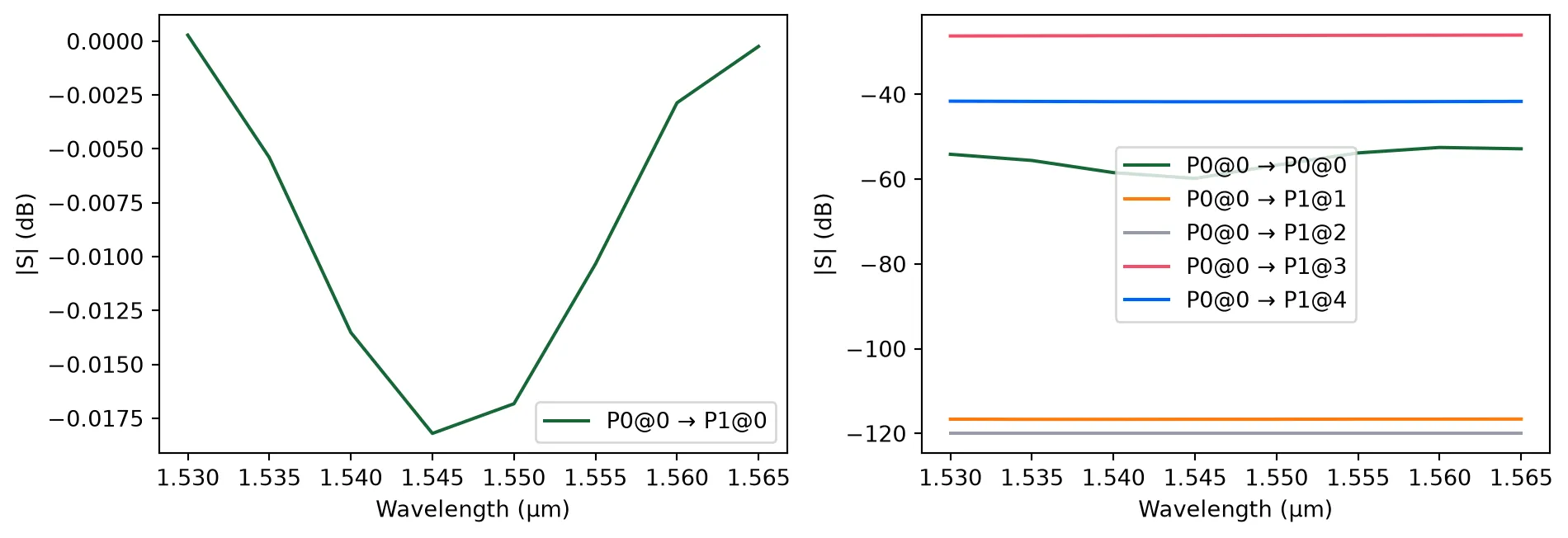
Y Spliter
Section titled “Y Spliter”The phase-shifter arms from the MZM are accessed by Y splitters in our design, so we also need to design it.
A simple S bend-based geometry can be used if the absolute lowest loss is not required:
@pf.parametric_component()def y_splitter(*, s_offset, taper_length=25):    c = pf.Component()
    core_width, _ = routing_spec.path_profile_for("LN_RIDGE")
    s_length = pf.s_bend_length(s_offset)
    for width, offset, layer in routing_spec.path_profiles:        input_taper = pf.Path((0, 0), width, offset=offset)        input_taper.segment((taper_length, 0), width + core_width)
        bottom_arm = pf.Path((taper_length, -0.5 * core_width), width, offset=offset)        bottom_arm.s_bend((taper_length + s_length, -s_offset))
        top_arm = pf.Path((taper_length, 0.5 * core_width), width, offset=offset)        top_arm.s_bend((taper_length + s_length, s_offset))
        # Heal the narrow regions for minimal feature size of approximately 100 nm        path_list = pf.heal(            [input_taper, bottom_arm, top_arm], 0.1 + pf.config.tolerance        )
        c.add(layer, *path_list)
    # Add ports    c.add_port(c.detect_ports([routing_spec]))
    # Add a model    c.add_model(pf.Tidy3DModel(), model_name="Tidy3D")
    return c
s_offset = 0.5 * (arms.ports["P1"].center[1] - arms.ports["P0"].center[1])splitter = y_splitter(s_offset=s_offset)viewer(splitter)
We can easily simulate it in Tidy3D over the C band. Before simulating, we add a field monitor so that we can visualize the simulated fields.
Note that the grid specification and shutoff arguments are given to reduce the simulation size at the cost of convergence. These should be removed if accurate results are needed.
# create a monitorfield_xy = td.FieldMonitor(    name="field_xy",    center=(0, 0, 0.2),    size=(td.inf, td.inf, 0),    freqs=[freqs[len(freqs) // 2]],)
# update the Tidy3DModel to add monitors_ = splitter.models["Tidy3D"].update(monitors=[field_xy])
s_matrix = splitter.s_matrix(frequencies=freqs, model_kwargs={"inputs": ["P0@0"]})Uploading task 'P0@0…'Starting task 'P0@0': https://tidy3d.simulation.cloud/workbench?taskId=fdve-106c48b9-3c09-46af-b83e-bca35aa87cc5Downloading data from 'P0@0'…_ = pf.plot_s_matrix(s_matrix, y="dB")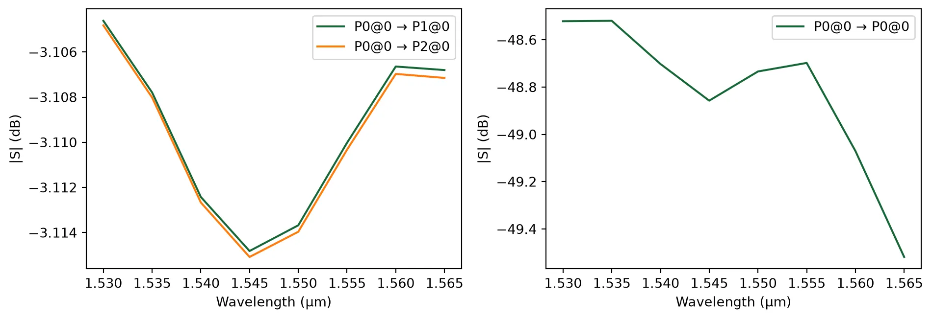
sim_data = splitter.models["Tidy3D"].batch_data(splitter, freqs, inputs=["P0@0"])sim_data.task_ids14:34:32 -03 Loading simulation from local cache. View cached task using web UI at 'https://tidy3d.simulation.cloud/workbench?taskId=fdve-106c48b9-3c0 9-46af-b83e-bca35aa87cc5'.
{'P0@0': 'fdve-106c48b9-3c09-46af-b83e-bca35aa87cc5'}# visualize the fieldsfig, ax = plt.subplots(1, 1, figsize=(10, 5))_ = sim_data["P0@0"].plot_field("field_xy", "E", "abs", robust=False, ax=ax)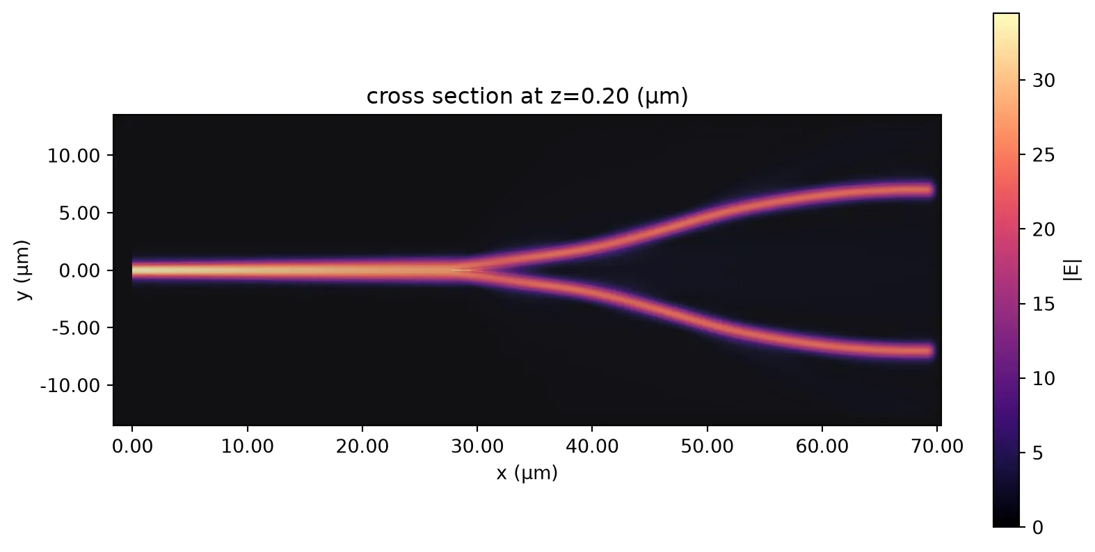
EO-MZM
Section titled “EO-MZM”Now add the splitters to the phase shifter arms to create the Mach-Zehnder interferometer, with an offset to separate both:
@pf.parametric_component()def eo_mzm():    netlist = {        "instances": {            "y_in": splitter,            "y_out": splitter,            "arms": arms,            "taper_in0": taper,            "taper_in1": taper,            "taper_out0": taper,            "taper_out1": taper,        },        "connections": [            (("taper_in0", "P0"), ("y_in", "P1")),            (("taper_in1", "P0"), ("y_in", "P2")),            (("arms", "P0"), ("taper_in0", "P1")),            (("taper_out0", "P1"), ("arms", "P2")),            (("taper_out1", "P1"), ("arms", "P3")),            (("y_out", "P1"), ("taper_out1", "P0")),        ],        "ports": [            ("y_in", "P0"),            ("y_out", "P0"),        ],        "models": [(pf.CircuitModel(), "Circuit")],    }
    return pf.component_from_netlist(netlist)
mzm = eo_mzm()viewer(mzm);fill:%23221f20;font-weight:bold;font-size:29.600000px;}.terminal{fill:none;stroke:%23805080;stroke-width:3.700000;}.dashed{stroke-dasharray:18.500000,11.100000;}.port{fill:none;stroke:%23805080;stroke-width:7.400000;}.virtual-connection{fill:none;stroke:%23907090;stroke-width:5.550000;}.layer_31_0{stroke:%23d4467c;fill:url(%23pat-layer_31_0);fill-opacity:0.492;}.label_31_0{fill:%23d4467c;}.layer_6_0{stroke:%237c605a;fill:url(%23pat-layer_6_0);fill-opacity:0.492;}.label_6_0{fill:%237c605a;}.layer_6_1{stroke:%2300d080;fill:url(%23pat-layer_6_1);fill-opacity:0.492;}.label_6_1{fill:%2300d080;}.layer_201_0{stroke:%23857b75;fill:url(%23pat-layer_201_0);fill-opacity:0.492;}.label_201_0{fill:%23857b75;}.layer_50_1{stroke:%23c7031c;fill:url(%23pat-layer_50_1);fill-opacity:0.492;}.label_50_1{fill:%23c7031c;}.layer_21_1{stroke:%233503fc;fill:url(%23pat-layer_21_1);fill-opacity:0.492;}.label_21_1{fill:%233503fc;}.layer_4_0{stroke:%235179b5;fill:url(%23pat-layer_4_0);fill-opacity:0.492;}.label_4_0{fill:%235179b5;}.layer_2_0{stroke:%237d57de;fill:url(%23pat-layer_2_0);fill-opacity:0.492;}.label_2_0{fill:%237d57de;}.layer_3_0{stroke:%23000080;fill:url(%23pat-layer_3_0);fill-opacity:0.492;}.label_3_0{fill:%23000080;}.layer_2_1{stroke:%23ff00ff;fill:url(%23pat-layer_2_1);fill-opacity:0.492;}.label_2_1{fill:%23ff00ff;}.layer_3_1{stroke:%236750bf;fill:url(%23pat-layer_3_1);fill-opacity:0.492;}.label_3_1{fill:%236750bf;}.layer_21_0{stroke:%233503fc;fill:url(%23pat-layer_21_0);fill-opacity:0.492;}.label_21_0{fill:%233503fc;}.layer_990_0{stroke:%23473328;fill:none;}.label_990_0{fill:%23473328;}</style><defs><path id=%22port-symbol%22 class=%22port%22 d=%22M 0,-14.800000 L 22.200000,0 0,14.800000%22 /><path id=%22ref-port-symbol%22 class=%22port%22 style=%22stroke-opacity:0.33;%22 d=%22M 0,-11.100000 C 14.800000,-11.100000 14.800000,11.100000 0,11.100000%22 /><circle id=%22port-bend-symbol%22 style=%22stroke-width:0;stroke:none;fill:%23805080;fill-opacity:1;%22 cx=%220%22 cy=%220%22 r=%226.660000%22 /><circle id=%22connection-symbol%22 style=%22stroke-width:0;stroke:none;fill:%23907090;fill-opacity:1;%22 cx=%220%22 cy=%220%22 r=%227.770000%22 /><pattern id=%22pat-layer_31_0%22 patternUnits=%22userSpaceOnUse%22 width=%2211.100000%22 height=%2211.100000%22 patternTransform=%22translate(8.488235,10.515789)%22><circle cx=%225.550000%22 cy=%225.550000%22 r=%221.850000%22 style=%22stroke:none;fill:%23d4467c;fill-opacity:1.0%22 /></pattern><pattern id=%22pat-layer_6_0%22 patternUnits=%22userSpaceOnUse%22 width=%2218.500000%22 height=%2218.500000%22 patternTransform=%22translate(8.705882,8.763158)%22><line x1=%220%22 y1=%229.250000%22 x2=%2218.500000%22 y2=%229.250000%22 style=%22stroke:%237c605a;stroke-width:1.850000%22 /></pattern><pattern id=%22pat-layer_6_1%22 patternUnits=%22userSpaceOnUse%22 width=%2211.100000%22 height=%2211.100000%22 patternTransform=%22translate(2.611765,7.010526)%22><line x1=%225.550000%22 y1=%220%22 x2=%225.550000%22 y2=%2211.100000%22 style=%22stroke:%2300d080;stroke-width:1.850000%22 /></pattern><pattern id=%22pat-layer_201_0%22 patternUnits=%22userSpaceOnUse%22 width=%2211.100000%22 height=%2211.100000%22 patternTransform=%22translate(8.488235,4.089474)%22><line x1=%225.550000%22 y1=%220%22 x2=%225.550000%22 y2=%2211.100000%22 style=%22stroke:%23857b75;stroke-width:1.850000%22 /><line x1=%220%22 y1=%225.550000%22 x2=%2211.100000%22 y2=%225.550000%22 style=%22stroke:%23857b75;stroke-width:1.850000%22 /></pattern><pattern id=%22pat-layer_50_1%22 patternUnits=%22userSpaceOnUse%22 width=%2211.100000%22 height=%2211.100000%22 patternTransform=%22translate(3.917647,1.168421)%22><line x1=%220%22 y1=%220%22 x2=%2211.100000%22 y2=%2211.100000%22 style=%22stroke:%23c7031c;stroke-width:1.850000%22 /><line x1=%22-5.550000%22 y1=%225.550000%22 x2=%225.550000%22 y2=%2216.650000%22 style=%22stroke:%23c7031c;stroke-width:1.850000%22 /><line x1=%225.550000%22 y1=%22-5.550000%22 x2=%2216.650000%22 y2=%225.550000%22 style=%22stroke:%23c7031c;stroke-width:1.850000%22 /><line x1=%2211.100000%22 y1=%220%22 x2=%220%22 y2=%2211.100000%22 style=%22stroke:%23c7031c;stroke-width:1.850000%22 /><line x1=%2216.650000%22 y1=%225.550000%22 x2=%225.550000%22 y2=%2216.650000%22 style=%22stroke:%23c7031c;stroke-width:1.850000%22 /><line x1=%225.550000%22 y1=%22-5.550000%22 x2=%22-5.550000%22 y2=%225.550000%22 style=%22stroke:%23c7031c;stroke-width:1.850000%22 /></pattern><pattern id=%22pat-layer_21_1%22 patternUnits=%22userSpaceOnUse%22 width=%2218.500000%22 height=%2218.500000%22 patternTransform=%22translate(7.617647,5.842105)%22><circle cx=%229.250000%22 cy=%229.250000%22 r=%221.850000%22 style=%22stroke:none;fill:%233503fc;fill-opacity:1.0%22 /></pattern><pattern id=%22pat-layer_4_0%22 patternUnits=%22userSpaceOnUse%22 width=%2218.500000%22 height=%2218.500000%22 patternTransform=%22translate(11.970588,5.842105)%22><line x1=%229.250000%22 y1=%220%22 x2=%229.250000%22 y2=%2218.500000%22 style=%22stroke:%235179b5;stroke-width:1.850000%22 /></pattern><pattern id=%22pat-layer_2_0%22 patternUnits=%22userSpaceOnUse%22 width=%2218.500000%22 height=%2218.500000%22 patternTransform=%22translate(15.235294,2.921053)%22><line x1=%220%22 y1=%220%22 x2=%2218.500000%22 y2=%2218.500000%22 style=%22stroke:%237d57de;stroke-width:1.850000%22 /><line x1=%22-9.250000%22 y1=%229.250000%22 x2=%229.250000%22 y2=%2227.750000%22 style=%22stroke:%237d57de;stroke-width:1.850000%22 /><line x1=%229.250000%22 y1=%22-9.250000%22 x2=%2227.750000%22 y2=%229.250000%22 style=%22stroke:%237d57de;stroke-width:1.850000%22 /></pattern><pattern id=%22pat-layer_3_0%22 patternUnits=%22userSpaceOnUse%22 width=%2211.100000%22 height=%2211.100000%22 patternTransform=%22translate(2.611765,8.178947)%22><line x1=%220%22 y1=%220%22 x2=%2211.100000%22 y2=%2211.100000%22 style=%22stroke:%23000080;stroke-width:1.850000%22 /><line x1=%22-5.550000%22 y1=%225.550000%22 x2=%225.550000%22 y2=%2216.650000%22 style=%22stroke:%23000080;stroke-width:1.850000%22 /><line x1=%225.550000%22 y1=%22-5.550000%22 x2=%2216.650000%22 y2=%225.550000%22 style=%22stroke:%23000080;stroke-width:1.850000%22 /></pattern><pattern id=%22pat-layer_2_1%22 patternUnits=%22userSpaceOnUse%22 width=%2211.100000%22 height=%2211.100000%22 patternTransform=%22translate(6.529412,3.505263)%22><line x1=%2211.100000%22 y1=%220%22 x2=%220%22 y2=%2211.100000%22 style=%22stroke:%23ff00ff;stroke-width:1.850000%22 /><line x1=%2216.650000%22 y1=%225.550000%22 x2=%225.550000%22 y2=%2216.650000%22 style=%22stroke:%23ff00ff;stroke-width:1.850000%22 /><line x1=%225.550000%22 y1=%22-5.550000%22 x2=%22-5.550000%22 y2=%225.550000%22 style=%22stroke:%23ff00ff;stroke-width:1.850000%22 /></pattern><pattern id=%22pat-layer_3_1%22 patternUnits=%22userSpaceOnUse%22 width=%2218.500000%22 height=%2218.500000%22 patternTransform=%22translate(0.000000,16.552632)%22><line x1=%220%22 y1=%220%22 x2=%2218.500000%22 y2=%2218.500000%22 style=%22stroke:%236750bf;stroke-width:1.850000%22 /><line x1=%22-9.250000%22 y1=%229.250000%22 x2=%229.250000%22 y2=%2227.750000%22 style=%22stroke:%236750bf;stroke-width:1.850000%22 /><line x1=%229.250000%22 y1=%22-9.250000%22 x2=%2227.750000%22 y2=%229.250000%22 style=%22stroke:%236750bf;stroke-width:1.850000%22 /></pattern><pattern id=%22pat-layer_21_0%22 patternUnits=%22userSpaceOnUse%22 width=%2211.100000%22 height=%2211.100000%22 patternTransform=%22translate(7.182353,1.752632)%22><line x1=%220%22 y1=%225.550000%22 x2=%2211.100000%22 y2=%225.550000%22 style=%22stroke:%233503fc;stroke-width:1.850000%22 /></pattern><g id=%22C1%22 data-name=%22y_splitter_s_7P000000000000001_t_25%22><path class=%22layer_2_0%22 d=%22M 68.715000,-6.500000 67.797000,-6.494000 66.879000,-6.477000 65.962000,-6.449000 65.045000,-6.410000 64.128000,-6.359000 63.212000,-6.297000 62.297000,-6.224000 61.383000,-6.139000 60.470000,-6.043000 59.559000,-5.936000 58.648000,-5.818000 57.740000,-5.688000 56.833000,-5.548000 55.927000,-5.396000 55.024000,-5.233000 54.123000,-5.059000 53.223000,-4.874000 52.327000,-4.678000 51.432000,-4.471000 50.541000,-4.253000 49.652000,-4.024000 48.766000,-3.784000 47.883000,-3.533000 47.010000,-3.274000 46.112000,-3.006000 45.254000,-2.763000 45.254000,-2.762000 44.319000,-2.509000 43.419000,-2.277000 42.554000,-2.066000 42.554000,-2.065000 41.544000,-1.831000 41.544000,-1.832000 40.699000,-1.647000 39.787000,-1.460000 38.875000,-1.284000 38.002000,-1.127000 38.002000,-1.126000 36.981000,-0.955000 36.981000,-0.956000 36.122000,-0.822000 35.200000,-0.691000 34.279000,-0.571000 33.401000,-0.468000 32.373000,-0.360000 32.373000,-0.361000 31.552000,-0.284000 30.520000,-0.201000 30.520000,-0.202000 29.648000,-0.143000 27.769000,-0.050000 27.769000,0.050000 29.648000,0.143000 30.520000,0.202000 31.552000,0.284000 32.373000,0.361000 32.373000,0.360000 33.401000,0.468000 34.279000,0.571000 35.200000,0.691000 36.122000,0.822000 36.981000,0.956000 36.981000,0.955000 38.002000,1.126000 38.002000,1.127000 38.875000,1.284000 39.787000,1.460000 40.699000,1.647000 41.544000,1.832000 41.544000,1.831000 42.554000,2.065000 42.554000,2.066000 43.419000,2.277000 44.319000,2.509000 45.254000,2.762000 45.254000,2.763000 46.112000,3.006000 47.010000,3.274000 47.883000,3.533000 48.766000,3.784000 49.652000,4.024000 50.541000,4.253000 51.432000,4.471000 52.327000,4.678000 53.223000,4.874000 54.123000,5.059000 55.024000,5.233000 55.927000,5.396000 56.833000,5.548000 57.739000,5.689000 58.648000,5.818000 59.559000,5.936000 60.470000,6.043000 61.383000,6.139000 62.297000,6.224000 63.212000,6.297000 64.128000,6.359000 65.045000,6.410000 65.962000,6.449000 66.879000,6.477000 67.797000,6.494000 68.715000,6.500000 68.715000,7.500000 67.785000,7.494000 66.804000,7.476000 66.804000,7.474000 65.925000,7.449000 64.996000,7.408000 64.067000,7.357000 63.141000,7.294000 63.140000,7.294000 62.161000,7.216000 62.161000,7.215000 61.287000,7.134000 60.311000,7.032000 60.311000,7.031000 59.435000,6.929000 58.514000,6.809000 57.593000,6.678000 56.677000,6.536000 55.709000,6.373000 54.840000,6.216000 53.928000,6.040000 53.016000,5.853000 52.113000,5.655000 52.112000,5.655000 51.156000,5.433000 50.296000,5.223000 49.396000,4.991000 48.455000,4.736000 47.603000,4.494000 46.645000,4.208000 45.832000,3.967000 44.949000,3.716000 44.063000,3.476000 43.174000,3.247000 42.283000,3.029000 41.388000,2.822000 40.492000,2.626000 39.592000,2.441000 38.691000,2.267000 37.788000,2.104000 36.882000,1.952000 35.975000,1.812000 35.067000,1.682000 34.156000,1.564000 33.245000,1.457000 32.332000,1.361000 31.418000,1.276000 30.503000,1.203000 29.587000,1.141000 28.670000,1.090000 27.753000,1.051000 26.836000,1.023000 25.918000,1.006000 25.001000,1.000000 25.000000,1.000000 12.500000,0.750000 0.000000,0.500000 0.000000,-0.500000 12.500000,-0.750000 25.000000,-1.000000 25.001000,-1.000000 25.918000,-1.006000 26.836000,-1.023000 27.753000,-1.051000 28.670000,-1.090000 29.587000,-1.141000 30.503000,-1.203000 31.418000,-1.276000 32.332000,-1.361000 33.245000,-1.457000 34.156000,-1.564000 35.067000,-1.682000 35.976000,-1.811000 36.882000,-1.952000 37.788000,-2.104000 38.691000,-2.267000 39.592000,-2.441000 40.492000,-2.626000 41.388000,-2.822000 42.283000,-3.029000 43.174000,-3.247000 44.063000,-3.476000 44.949000,-3.716000 45.832000,-3.967000 46.645000,-4.208000 47.603000,-4.494000 48.455000,-4.736000 49.396000,-4.991000 50.296000,-5.223000 51.156000,-5.433000 52.112000,-5.655000 52.113000,-5.655000 53.016000,-5.853000 53.928000,-6.040000 54.840000,-6.216000 55.709000,-6.372000 55.709000,-6.373000 56.677000,-6.536000 57.593000,-6.678000 58.515000,-6.809000 59.435000,-6.929000 60.311000,-7.031000 60.311000,-7.032000 61.287000,-7.134000 62.161000,-7.215000 62.161000,-7.216000 63.140000,-7.294000 63.141000,-7.294000 64.067000,-7.357000 64.996000,-7.408000 65.925000,-7.449000 66.804000,-7.474000 66.804000,-7.476000 67.785000,-7.494000 68.715000,-7.500000 z%22 /><path class=%22layer_3_0%22 d=%22M 68.715000,-2.000000 67.852000,-1.995000 66.990000,-1.979000 65.266000,-1.915000 63.544000,-1.809000 62.684000,-1.740000 61.825000,-1.661000 60.968000,-1.571000 60.111000,-1.470000 59.255000,-1.359000 58.401000,-1.237000 57.549000,-1.105000 56.698000,-0.963000 55.849000,-0.810000 55.002000,-0.646000 53.315000,-0.288000 52.475000,-0.094000 52.091000,0.000000 52.475000,0.094000 53.315000,0.288000 55.002000,0.646000 55.849000,0.810000 56.698000,0.963000 57.549000,1.105000 58.401000,1.237000 59.255000,1.359000 60.111000,1.470000 60.968000,1.571000 61.825000,1.661000 62.684000,1.740000 63.544000,1.809000 65.266000,1.915000 66.990000,1.979000 67.852000,1.995000 68.715000,2.000000 68.715000,12.000000 67.729000,11.994000 66.744000,11.976000 65.759000,11.945000 64.774000,11.903000 63.790000,11.849000 62.807000,11.782000 61.774000,11.699000 61.774000,11.698000 60.843000,11.612000 59.862000,11.510000 58.884000,11.395000 57.906000,11.268000 56.932000,11.129000 55.957000,10.978000 54.985000,10.815000 54.015000,10.640000 53.047000,10.453000 52.081000,10.255000 51.119000,10.044000 50.159000,9.822000 49.200000,9.587000 48.247000,9.342000 47.296000,9.084000 46.347000,8.815000 45.441000,8.545000 44.576000,8.288000 43.746000,8.052000 42.078000,7.611000 41.240000,7.406000 40.400000,7.212000 38.713000,6.854000 37.866000,6.690000 37.017000,6.537000 36.166000,6.395000 35.314000,6.263000 34.460000,6.141000 33.604000,6.030000 32.747000,5.929000 31.890000,5.839000 31.031000,5.760000 30.171000,5.691000 28.449000,5.585000 26.725000,5.521000 25.863000,5.505000 25.000000,5.500000 12.500000,5.250000 0.000000,5.000000 0.000000,-5.000000 12.500000,-5.250000 25.000000,-5.500000 25.863000,-5.505000 26.725000,-5.521000 28.449000,-5.585000 29.310000,-5.633000 30.171000,-5.691000 31.031000,-5.760000 31.890000,-5.839000 32.747000,-5.929000 33.604000,-6.030000 34.460000,-6.141000 35.314000,-6.263000 36.166000,-6.395000 37.017000,-6.537000 37.866000,-6.690000 38.713000,-6.854000 40.400000,-7.212000 41.240000,-7.406000 42.078000,-7.611000 43.746000,-8.052000 44.576000,-8.288000 45.441000,-8.545000 46.347000,-8.815000 47.296000,-9.084000 48.247000,-9.342000 49.200000,-9.587000 50.159000,-9.822000 51.120000,-10.044000 52.081000,-10.255000 53.047000,-10.453000 54.015000,-10.640000 54.985000,-10.815000 55.958000,-10.978000 56.932000,-11.129000 57.906000,-11.268000 58.883000,-11.395000 59.814000,-11.503000 59.814000,-11.504000 60.845000,-11.612000 61.774000,-11.698000 61.774000,-11.699000 62.807000,-11.782000 63.791000,-11.848000 64.775000,-11.903000 65.759000,-11.945000 66.744000,-11.976000 67.729000,-11.994000 68.715000,-12.000000 z%22 /></g><g id=%22C2%22 data-name=%22mzm_arms_l_3000_t_150%22><use transform=%22translate(0.000000 0.000000)%22 href=%22%23C4%22 /><use transform=%22translate(0.000000 -7.000000)%22 href=%22%23C5%22 /><use transform=%22translate(0.000000 7.000000)%22 href=%22%23C5%22 /><use transform=%22translate(-150.000000 0.000000)%22 href=%22%23C6%22 /><use transform=%22translate(3150.000000 0.000000)%22 href=%22%23C6%22 /><use transform=%22translate(0.000000 0.000000)%22 href=%22%23C7%22 /><use transform=%22translate(0.000000 0.000000)%22 href=%22%23C8%22 /><use transform=%22translate(0.000000 0.000000)%22 href=%22%23C9%22 /><use transform=%22translate(0.000000 0.000000)%22 href=%22%23C10%22 /><use transform=%22translate(0.000000 0.000000)%22 href=%22%23C11%22 /><use transform=%22translate(0.000000 0.000000)%22 href=%22%23C12%22 /><rect class=%22terminal dashed%22 x=%22-200.000000%22 y=%22-200.000000%22 width=%22100.000000%22 height=%22100.000000%22 /><rect class=%22terminal dashed%22 x=%223100.000000%22 y=%22-200.000000%22 width=%22100.000000%22 height=%22100.000000%22 /><rect class=%22terminal dashed%22 x=%22-200.000000%22 y=%22100.000000%22 width=%22100.000000%22 height=%22100.000000%22 /><rect class=%22terminal dashed%22 x=%223100.000000%22 y=%22100.000000%22 width=%22100.000000%22 height=%22100.000000%22 /><rect class=%22terminal dashed%22 x=%22-200.000000%22 y=%22-50.000000%22 width=%22100.000000%22 height=%22100.000000%22 /><rect class=%22terminal dashed%22 x=%223100.000000%22 y=%22-50.000000%22 width=%22100.000000%22 height=%22100.000000%22 /></g><g id=%22C3%22 data-name=%22transition__AMNY2TPUX3FKPYS7E4ISTHC72RJF7QOUXPWAT4TFOMHDLLGSIF4A%22><path class=%22layer_2_0%22 d=%22M 0.000000,-0.500000 4.000000,-0.700000 8.000000,-0.900000 12.000000,-1.100000 16.000000,-1.300000 20.000000,-1.500000 20.000000,1.500000 16.000000,1.300000 12.000000,1.100000 8.000000,0.900000 4.000000,0.700000 0.000000,0.500000 z%22 /><path class=%22layer_3_0%22 d=%22M 0.000000,-5.000000 4.000000,-5.200000 8.000000,-5.400000 12.000000,-5.600000 16.000000,-5.800000 20.000000,-6.000000 20.000000,6.000000 16.000000,5.800000 12.000000,5.600000 8.000000,5.400000 4.000000,5.200000 0.000000,5.000000 z%22 /></g><g id=%22C10%22 data-name=%22route_taper__WNDRC65BALYZPNB7XX3FEBC2UGZEKYKCY7M4VLNKXEHQN2GAF4DQ%22><path class=%22layer_21_0%22 d=%22M 3000.000000,-9.000000 3000.000000,-189.000000 3100.000000,-200.000000 3200.000000,-200.000000 3200.000000,-100.000000 3100.000000,-100.000000 z%22 /><rect class=%22terminal dashed%22 x=%223100.000000%22 y=%22-200.000000%22 width=%22100.000000%22 height=%22100.000000%22 /><rect class=%22terminal dashed%22 x=%223000.000000%22 y=%22-189.000000%22 width=%220.000000%22 height=%22180.000000%22 transform=%22translate(3000.000000 -99.000000) rotate(180.000000) translate(-3000.000000 99.000000)%22 /></g><g id=%22C11%22 data-name=%22route_taper__ES2DXYTUQAS74DGIJQQRQH26CLX3VUSNG4GLWD2N7OCBV4KLEZLQ%22><path class=%22layer_21_0%22 d=%22M 3000.000000,5.000000 3000.000000,-5.000000 3100.000000,-50.000000 3200.000000,-50.000000 3200.000000,50.000000 3100.000000,50.000000 z%22 /><rect class=%22terminal dashed%22 x=%223100.000000%22 y=%22-50.000000%22 width=%22100.000000%22 height=%22100.000000%22 /><rect class=%22terminal dashed%22 x=%223000.000000%22 y=%22-5.000000%22 width=%220.000000%22 height=%2210.000000%22 transform=%22translate(3000.000000 0.000000) rotate(180.000000) translate(-3000.000000 -0.000000)%22 /></g><g id=%22C12%22 data-name=%22route_taper__EX2QKAKHVK7NLR3BPYWBESMWGPFO3TP7S3NZRYPWWCIOIN24HLVA%22><path class=%22layer_21_0%22 d=%22M 3000.000000,189.000000 3000.000000,9.000000 3100.000000,100.000000 3200.000000,100.000000 3200.000000,200.000000 3100.000000,200.000000 z%22 /><rect class=%22terminal dashed%22 x=%223100.000000%22 y=%22100.000000%22 width=%22100.000000%22 height=%22100.000000%22 /><rect class=%22terminal dashed%22 x=%223000.000000%22 y=%229.000000%22 width=%220.000000%22 height=%22180.000000%22 transform=%22translate(3000.000000 99.000000) rotate(180.000000) translate(-3000.000000 -99.000000)%22 /></g><g id=%22C4%22 data-name=%22straight__AG6SILVP37K2TEZZWX3AT24APB5V2ZFF2EQZCHJ7MFLQSWV5WG3Q%22><path class=%22layer_21_0%22 d=%22M 0.000000,-189.000000 3000.000000,-189.000000 3000.000000,-9.000000 0.000000,-9.000000 z%22 /><path class=%22layer_21_0%22 d=%22M 0.000000,9.000000 3000.000000,9.000000 3000.000000,189.000000 0.000000,189.000000 z%22 /><path class=%22layer_21_0%22 d=%22M 0.000000,-5.000000 3000.000000,-5.000000 3000.000000,5.000000 0.000000,5.000000 z%22 /></g><g id=%22C5%22 data-name=%22straight__COQUAEHJ3TMV6MSBWNCAOFHBICTW7SBMD3WQGXAUREJWA5HFT2EA%22><path class=%22layer_2_0%22 d=%22M 0.000000,-1.500000 3000.000000,-1.500000 3000.000000,1.500000 0.000000,1.500000 z%22 /><path class=%22layer_3_0%22 d=%22M 0.000000,-6.000000 3000.000000,-6.000000 3000.000000,6.000000 0.000000,6.000000 z%22 /></g><g id=%22C6%22 data-name=%22gsg_pad__EHZT4TPCDWNKDTN7XW5UFRPU6DHM2SJETLFKVCGZI6SCYBGCMJ3Q%22><rect class=%22terminal dashed%22 x=%22-50.000000%22 y=%22-200.000000%22 width=%22100.000000%22 height=%22100.000000%22 /><rect class=%22terminal dashed%22 x=%22-50.000000%22 y=%22100.000000%22 width=%22100.000000%22 height=%22100.000000%22 /><rect class=%22terminal dashed%22 x=%22-50.000000%22 y=%22-50.000000%22 width=%22100.000000%22 height=%22100.000000%22 /></g><g id=%22C7%22 data-name=%22route_taper__M2ROCEGOJLW3HT7CARRZUGQ6ZZVBXEDEJVO6TLBFOKEJ7GFKPSIQ%22><path class=%22layer_21_0%22 d=%22M -100.000000,-100.000000 -200.000000,-100.000000 -200.000000,-200.000000 -100.000000,-200.000000 0.000000,-189.000000 0.000000,-9.000000 z%22 /><rect class=%22terminal dashed%22 x=%22-200.000000%22 y=%22-200.000000%22 width=%22100.000000%22 height=%22100.000000%22 /><rect class=%22terminal dashed%22 x=%220.000000%22 y=%22-189.000000%22 width=%220.000000%22 height=%22180.000000%22 /></g><g id=%22C8%22 data-name=%22route_taper__3FI24T52I5STIIBAEYXOT3OJODLXCZ7ODECZUAQYWKMXI6YTFU6A%22><path class=%22layer_21_0%22 d=%22M -100.000000,50.000000 -200.000000,50.000000 -200.000000,-50.000000 -100.000000,-50.000000 0.000000,-5.000000 0.000000,5.000000 z%22 /><rect class=%22terminal dashed%22 x=%22-200.000000%22 y=%22-50.000000%22 width=%22100.000000%22 height=%22100.000000%22 /><rect class=%22terminal dashed%22 x=%220.000000%22 y=%22-5.000000%22 width=%220.000000%22 height=%2210.000000%22 /></g><g id=%22C9%22 data-name=%22route_taper__5KJBAW27FA63EAP3RJXMXB6SX3FDZNEIOSLYYKFBH7C6VIWWBXNA%22><path class=%22layer_21_0%22 d=%22M -100.000000,200.000000 -200.000000,200.000000 -200.000000,100.000000 -100.000000,100.000000 0.000000,9.000000 0.000000,189.000000 z%22 /><rect class=%22terminal dashed%22 x=%22-200.000000%22 y=%22100.000000%22 width=%22100.000000%22 height=%22100.000000%22 /><rect class=%22terminal dashed%22 x=%220.000000%22 y=%229.000000%22 width=%220.000000%22 height=%22180.000000%22 /></g></defs><g transform=%22scale(1 -1)%22><g id=%22C0%22 data-name=%22eo_mzm%22><use transform=%22translate(0.000000 0.000000)%22 href=%22%23C1%22 /><use transform=%22translate(3177.430000 0.000000) rotate(180.000000)%22 href=%22%23C1%22 /><use transform=%22translate(88.715000 0.000000)%22 href=%22%23C2%22 /><use transform=%22translate(68.715000 -7.000000)%22 href=%22%23C3%22 /><use transform=%22translate(68.715000 7.000000)%22 href=%22%23C3%22 /><use transform=%22translate(3108.715000 -7.000000) rotate(180.000000)%22 href=%22%23C3%22 /><use transform=%22translate(3108.715000 7.000000) rotate(180.000000)%22 href=%22%23C3%22 /><g transform=%22translate(0.000000 0.000000) rotate(0.000000)%22><path class=%22port%22 d=%22M 0,-2.500000 V 2.500000%22 /><use href=%22%23port-symbol%22 /></g><text class=%22label%22 text-anchor=%22start%22 dominant-baseline=%22text-after-edge%22 x=%220.000000%22 y=%22-0.000000%22>P0</text><g transform=%22translate(3177.430000 0.000000) rotate(180.000000)%22><path class=%22port%22 d=%22M 0,-2.500000 V 2.500000%22 /><use href=%22%23port-symbol%22 /></g><text class=%22label%22 text-anchor=%22end%22 dominant-baseline=%22text-before-edge%22 x=%223177.430000%22 y=%22-0.000000%22>P1</text></g></g></svg>)
Edge Coupler
Section titled “Edge Coupler”The original work [1] uses a simple transition to a 2.5 μm-wide waveguide at the chip edges to couple to lensed fibers.
Optimizing the length and tapering profile of such a device can be easily done within PhotonForge using, e.g. Monte Carlo sweeps. An example of design can be found in our edge coupler notebook.
For the purpose of this example, we will simply use a PDK-provided edge coupler.
edge_coupler = lxt.component.edge_coupler()viewer(edge_coupler)
Full Chip
Section titled “Full Chip”We integrate the edge couplers with the MZM and create a complete device for testing. As a reference, we should also create a straight waveguide link to evaluate the coupling losses. These components are created by a single parametric function to improve consistency:
@pf.parametric_component()def coupled_device(*, full_length=4000, coupler_length=20, reference_link=False):    c = pf.Component()
    in_coupler = pf.Reference(edge_coupler)    out_coupler = pf.Reference(edge_coupler, origin=(full_length, 0), rotation=180)    c.add(in_coupler, out_coupler)
    if reference_link:        c.add(pf.parametric.route(port1=in_coupler["P1"], port2=out_coupler["P1"]))    else:        mzm_ref = c.add_reference(mzm)        mzm_ref.x_mid = full_length / 2
        if mzm_ref["P0"].center[0] < in_coupler["P1"].center[0]:            raise RuntimeError("Device not long enough for the desired MZM.")
        c.add(            pf.parametric.route(port1=in_coupler["P1"], port2=mzm_ref["P0"]),            pf.parametric.route(port1=out_coupler["P1"], port2=mzm_ref["P1"]),        )
    c.add_port([in_coupler["P0"], out_coupler["P0"]])
    c.add_model(pf.CircuitModel(), "Circuit")
    return c
device = coupled_device()viewer(device);fill:%23221f20;font-weight:bold;font-size:32.000000px;}.terminal{fill:none;stroke:%23805080;stroke-width:4.000000;}.dashed{stroke-dasharray:20.000000,12.000000;}.port{fill:none;stroke:%23805080;stroke-width:8.000000;}.virtual-connection{fill:none;stroke:%23907090;stroke-width:6.000000;}.layer_31_0{stroke:%23d4467c;fill:url(%23pat-layer_31_0);fill-opacity:0.492;}.label_31_0{fill:%23d4467c;}.layer_6_0{stroke:%237c605a;fill:url(%23pat-layer_6_0);fill-opacity:0.492;}.label_6_0{fill:%237c605a;}.layer_6_1{stroke:%2300d080;fill:url(%23pat-layer_6_1);fill-opacity:0.492;}.label_6_1{fill:%2300d080;}.layer_201_0{stroke:%23857b75;fill:url(%23pat-layer_201_0);fill-opacity:0.492;}.label_201_0{fill:%23857b75;}.layer_50_1{stroke:%23c7031c;fill:url(%23pat-layer_50_1);fill-opacity:0.492;}.label_50_1{fill:%23c7031c;}.layer_21_1{stroke:%233503fc;fill:url(%23pat-layer_21_1);fill-opacity:0.492;}.label_21_1{fill:%233503fc;}.layer_4_0{stroke:%235179b5;fill:url(%23pat-layer_4_0);fill-opacity:0.492;}.label_4_0{fill:%235179b5;}.layer_2_0{stroke:%237d57de;fill:url(%23pat-layer_2_0);fill-opacity:0.492;}.label_2_0{fill:%237d57de;}.layer_3_0{stroke:%23000080;fill:url(%23pat-layer_3_0);fill-opacity:0.492;}.label_3_0{fill:%23000080;}.layer_2_1{stroke:%23ff00ff;fill:url(%23pat-layer_2_1);fill-opacity:0.492;}.label_2_1{fill:%23ff00ff;}.layer_3_1{stroke:%236750bf;fill:url(%23pat-layer_3_1);fill-opacity:0.492;}.label_3_1{fill:%236750bf;}.layer_21_0{stroke:%233503fc;fill:url(%23pat-layer_21_0);fill-opacity:0.492;}.label_21_0{fill:%233503fc;}.layer_990_0{stroke:%23473328;fill:none;}.label_990_0{fill:%23473328;}</style><defs><path id=%22port-symbol%22 class=%22port%22 d=%22M 0,-16.000000 L 24.000000,0 0,16.000000%22 /><path id=%22ref-port-symbol%22 class=%22port%22 style=%22stroke-opacity:0.33;%22 d=%22M 0,-12.000000 C 16.000000,-12.000000 16.000000,12.000000 0,12.000000%22 /><circle id=%22port-bend-symbol%22 style=%22stroke-width:0;stroke:none;fill:%23805080;fill-opacity:1;%22 cx=%220%22 cy=%220%22 r=%227.200000%22 /><circle id=%22connection-symbol%22 style=%22stroke-width:0;stroke:none;fill:%23907090;fill-opacity:1;%22 cx=%220%22 cy=%220%22 r=%228.400000%22 /><pattern id=%22pat-layer_31_0%22 patternUnits=%22userSpaceOnUse%22 width=%2212.000000%22 height=%2212.000000%22 patternTransform=%22translate(9.176471,11.368421)%22><circle cx=%226.000000%22 cy=%226.000000%22 r=%222.000000%22 style=%22stroke:none;fill:%23d4467c;fill-opacity:1.0%22 /></pattern><pattern id=%22pat-layer_6_0%22 patternUnits=%22userSpaceOnUse%22 width=%2220.000000%22 height=%2220.000000%22 patternTransform=%22translate(9.411765,9.473684)%22><line x1=%220%22 y1=%2210.000000%22 x2=%2220.000000%22 y2=%2210.000000%22 style=%22stroke:%237c605a;stroke-width:2.000000%22 /></pattern><pattern id=%22pat-layer_6_1%22 patternUnits=%22userSpaceOnUse%22 width=%2212.000000%22 height=%2212.000000%22 patternTransform=%22translate(2.823529,7.578947)%22><line x1=%226.000000%22 y1=%220%22 x2=%226.000000%22 y2=%2212.000000%22 style=%22stroke:%2300d080;stroke-width:2.000000%22 /></pattern><pattern id=%22pat-layer_201_0%22 patternUnits=%22userSpaceOnUse%22 width=%2212.000000%22 height=%2212.000000%22 patternTransform=%22translate(9.176471,4.421053)%22><line x1=%226.000000%22 y1=%220%22 x2=%226.000000%22 y2=%2212.000000%22 style=%22stroke:%23857b75;stroke-width:2.000000%22 /><line x1=%220%22 y1=%226.000000%22 x2=%2212.000000%22 y2=%226.000000%22 style=%22stroke:%23857b75;stroke-width:2.000000%22 /></pattern><pattern id=%22pat-layer_50_1%22 patternUnits=%22userSpaceOnUse%22 width=%2212.000000%22 height=%2212.000000%22 patternTransform=%22translate(4.235294,1.263158)%22><line x1=%220%22 y1=%220%22 x2=%2212.000000%22 y2=%2212.000000%22 style=%22stroke:%23c7031c;stroke-width:2.000000%22 /><line x1=%22-6.000000%22 y1=%226.000000%22 x2=%226.000000%22 y2=%2218.000000%22 style=%22stroke:%23c7031c;stroke-width:2.000000%22 /><line x1=%226.000000%22 y1=%22-6.000000%22 x2=%2218.000000%22 y2=%226.000000%22 style=%22stroke:%23c7031c;stroke-width:2.000000%22 /><line x1=%2212.000000%22 y1=%220%22 x2=%220%22 y2=%2212.000000%22 style=%22stroke:%23c7031c;stroke-width:2.000000%22 /><line x1=%2218.000000%22 y1=%226.000000%22 x2=%226.000000%22 y2=%2218.000000%22 style=%22stroke:%23c7031c;stroke-width:2.000000%22 /><line x1=%226.000000%22 y1=%22-6.000000%22 x2=%22-6.000000%22 y2=%226.000000%22 style=%22stroke:%23c7031c;stroke-width:2.000000%22 /></pattern><pattern id=%22pat-layer_21_1%22 patternUnits=%22userSpaceOnUse%22 width=%2220.000000%22 height=%2220.000000%22 patternTransform=%22translate(8.235294,6.315789)%22><circle cx=%2210.000000%22 cy=%2210.000000%22 r=%222.000000%22 style=%22stroke:none;fill:%233503fc;fill-opacity:1.0%22 /></pattern><pattern id=%22pat-layer_4_0%22 patternUnits=%22userSpaceOnUse%22 width=%2220.000000%22 height=%2220.000000%22 patternTransform=%22translate(12.941176,6.315789)%22><line x1=%2210.000000%22 y1=%220%22 x2=%2210.000000%22 y2=%2220.000000%22 style=%22stroke:%235179b5;stroke-width:2.000000%22 /></pattern><pattern id=%22pat-layer_2_0%22 patternUnits=%22userSpaceOnUse%22 width=%2220.000000%22 height=%2220.000000%22 patternTransform=%22translate(16.470588,3.157895)%22><line x1=%220%22 y1=%220%22 x2=%2220.000000%22 y2=%2220.000000%22 style=%22stroke:%237d57de;stroke-width:2.000000%22 /><line x1=%22-10.000000%22 y1=%2210.000000%22 x2=%2210.000000%22 y2=%2230.000000%22 style=%22stroke:%237d57de;stroke-width:2.000000%22 /><line x1=%2210.000000%22 y1=%22-10.000000%22 x2=%2230.000000%22 y2=%2210.000000%22 style=%22stroke:%237d57de;stroke-width:2.000000%22 /></pattern><pattern id=%22pat-layer_3_0%22 patternUnits=%22userSpaceOnUse%22 width=%2212.000000%22 height=%2212.000000%22 patternTransform=%22translate(2.823529,8.842105)%22><line x1=%220%22 y1=%220%22 x2=%2212.000000%22 y2=%2212.000000%22 style=%22stroke:%23000080;stroke-width:2.000000%22 /><line x1=%22-6.000000%22 y1=%226.000000%22 x2=%226.000000%22 y2=%2218.000000%22 style=%22stroke:%23000080;stroke-width:2.000000%22 /><line x1=%226.000000%22 y1=%22-6.000000%22 x2=%2218.000000%22 y2=%226.000000%22 style=%22stroke:%23000080;stroke-width:2.000000%22 /></pattern><pattern id=%22pat-layer_2_1%22 patternUnits=%22userSpaceOnUse%22 width=%2212.000000%22 height=%2212.000000%22 patternTransform=%22translate(7.058824,3.789474)%22><line x1=%2212.000000%22 y1=%220%22 x2=%220%22 y2=%2212.000000%22 style=%22stroke:%23ff00ff;stroke-width:2.000000%22 /><line x1=%2218.000000%22 y1=%226.000000%22 x2=%226.000000%22 y2=%2218.000000%22 style=%22stroke:%23ff00ff;stroke-width:2.000000%22 /><line x1=%226.000000%22 y1=%22-6.000000%22 x2=%22-6.000000%22 y2=%226.000000%22 style=%22stroke:%23ff00ff;stroke-width:2.000000%22 /></pattern><pattern id=%22pat-layer_3_1%22 patternUnits=%22userSpaceOnUse%22 width=%2220.000000%22 height=%2220.000000%22 patternTransform=%22translate(0.000000,17.894737)%22><line x1=%220%22 y1=%220%22 x2=%2220.000000%22 y2=%2220.000000%22 style=%22stroke:%236750bf;stroke-width:2.000000%22 /><line x1=%22-10.000000%22 y1=%2210.000000%22 x2=%2210.000000%22 y2=%2230.000000%22 style=%22stroke:%236750bf;stroke-width:2.000000%22 /><line x1=%2210.000000%22 y1=%22-10.000000%22 x2=%2230.000000%22 y2=%2210.000000%22 style=%22stroke:%236750bf;stroke-width:2.000000%22 /></pattern><pattern id=%22pat-layer_21_0%22 patternUnits=%22userSpaceOnUse%22 width=%2212.000000%22 height=%2212.000000%22 patternTransform=%22translate(7.764706,1.894737)%22><line x1=%220%22 y1=%226.000000%22 x2=%2212.000000%22 y2=%226.000000%22 style=%22stroke:%233503fc;stroke-width:2.000000%22 /></pattern><g id=%22C1%22 data-name=%22edge_coupler__D4E7NKX2GQ3U2736LLE4YDC3XWAYHPRUI55W2MOYTHNRCAOLWJFA%22><path class=%22layer_2_0%22 d=%22M 120.000000,-0.125000 360.000000,-0.500000 360.000000,0.500000 120.000000,0.125000 z%22 /><path class=%22layer_3_0%22 d=%22M 0.000000,-0.125000 360.000000,-2.825000 360.000000,2.825000 0.000000,0.125000 z%22 /><rect class=%22layer_3_1%22 x=%220.000000%22 y=%22-10.000000%22 width=%22360.000000%22 height=%2220.000000%22 /></g><g id=%22C2%22 data-name=%22eo_mzm%22><use transform=%22translate(0.000000 0.000000)%22 href=%22%23C5%22 /><use transform=%22translate(3177.430000 0.000000) rotate(180.000000)%22 href=%22%23C5%22 /><use transform=%22translate(88.715000 0.000000)%22 href=%22%23C6%22 /><use transform=%22translate(68.715000 -7.000000)%22 href=%22%23C7%22 /><use transform=%22translate(68.715000 7.000000)%22 href=%22%23C7%22 /><use transform=%22translate(3108.715000 -7.000000) rotate(180.000000)%22 href=%22%23C7%22 /><use transform=%22translate(3108.715000 7.000000) rotate(180.000000)%22 href=%22%23C7%22 /></g><g id=%22C3%22 data-name=%22route__JGQXTMPF44NCZ2DMOETORXSFGANAFZZPHZNUSDBC4KXDC3HM2DJQ%22><use transform=%22translate(360.000000 0.000000)%22 href=%22%23C8%22 /></g><g id=%22C4%22 data-name=%22route__HSF6N3VZV3X6RX7F2NXA4ZJVIYTF3ESBCACGF5Z5XL4UBVOJ3OUA%22><use transform=%22translate(3640.000000 0.000000) rotate(180.000000)%22 href=%22%23C8%22 /></g><g id=%22C5%22 data-name=%22y_splitter_s_7P000000000000001_t_25%22><path class=%22layer_2_0%22 d=%22M 68.715000,-6.500000 67.797000,-6.494000 66.879000,-6.477000 65.962000,-6.449000 65.045000,-6.410000 64.128000,-6.359000 63.212000,-6.297000 62.297000,-6.224000 61.383000,-6.139000 60.470000,-6.043000 59.559000,-5.936000 58.648000,-5.818000 57.740000,-5.688000 56.833000,-5.548000 55.927000,-5.396000 55.024000,-5.233000 54.123000,-5.059000 53.223000,-4.874000 52.327000,-4.678000 51.432000,-4.471000 50.541000,-4.253000 49.652000,-4.024000 48.766000,-3.784000 47.883000,-3.533000 47.010000,-3.274000 46.112000,-3.006000 45.254000,-2.763000 45.254000,-2.762000 44.319000,-2.509000 43.419000,-2.277000 42.554000,-2.066000 42.554000,-2.065000 41.544000,-1.831000 41.544000,-1.832000 40.699000,-1.647000 39.787000,-1.460000 38.875000,-1.284000 38.002000,-1.127000 38.002000,-1.126000 36.981000,-0.955000 36.981000,-0.956000 36.122000,-0.822000 35.200000,-0.691000 34.279000,-0.571000 33.401000,-0.468000 32.373000,-0.360000 32.373000,-0.361000 31.552000,-0.284000 30.520000,-0.201000 30.520000,-0.202000 29.648000,-0.143000 27.769000,-0.050000 27.769000,0.050000 29.648000,0.143000 30.520000,0.202000 31.552000,0.284000 32.373000,0.361000 32.373000,0.360000 33.401000,0.468000 34.279000,0.571000 35.200000,0.691000 36.122000,0.822000 36.981000,0.956000 36.981000,0.955000 38.002000,1.126000 38.002000,1.127000 38.875000,1.284000 39.787000,1.460000 40.699000,1.647000 41.544000,1.832000 41.544000,1.831000 42.554000,2.065000 42.554000,2.066000 43.419000,2.277000 44.319000,2.509000 45.254000,2.762000 45.254000,2.763000 46.112000,3.006000 47.010000,3.274000 47.883000,3.533000 48.766000,3.784000 49.652000,4.024000 50.541000,4.253000 51.432000,4.471000 52.327000,4.678000 53.223000,4.874000 54.123000,5.059000 55.024000,5.233000 55.927000,5.396000 56.833000,5.548000 57.739000,5.689000 58.648000,5.818000 59.559000,5.936000 60.470000,6.043000 61.383000,6.139000 62.297000,6.224000 63.212000,6.297000 64.128000,6.359000 65.045000,6.410000 65.962000,6.449000 66.879000,6.477000 67.797000,6.494000 68.715000,6.500000 68.715000,7.500000 67.785000,7.494000 66.804000,7.476000 66.804000,7.474000 65.925000,7.449000 64.996000,7.408000 64.067000,7.357000 63.141000,7.294000 63.140000,7.294000 62.161000,7.216000 62.161000,7.215000 61.287000,7.134000 60.311000,7.032000 60.311000,7.031000 59.435000,6.929000 58.514000,6.809000 57.593000,6.678000 56.677000,6.536000 55.709000,6.373000 54.840000,6.216000 53.928000,6.040000 53.016000,5.853000 52.113000,5.655000 52.112000,5.655000 51.156000,5.433000 50.296000,5.223000 49.396000,4.991000 48.455000,4.736000 47.603000,4.494000 46.645000,4.208000 45.832000,3.967000 44.949000,3.716000 44.063000,3.476000 43.174000,3.247000 42.283000,3.029000 41.388000,2.822000 40.492000,2.626000 39.592000,2.441000 38.691000,2.267000 37.788000,2.104000 36.882000,1.952000 35.975000,1.812000 35.067000,1.682000 34.156000,1.564000 33.245000,1.457000 32.332000,1.361000 31.418000,1.276000 30.503000,1.203000 29.587000,1.141000 28.670000,1.090000 27.753000,1.051000 26.836000,1.023000 25.918000,1.006000 25.001000,1.000000 25.000000,1.000000 12.500000,0.750000 0.000000,0.500000 0.000000,-0.500000 12.500000,-0.750000 25.000000,-1.000000 25.001000,-1.000000 25.918000,-1.006000 26.836000,-1.023000 27.753000,-1.051000 28.670000,-1.090000 29.587000,-1.141000 30.503000,-1.203000 31.418000,-1.276000 32.332000,-1.361000 33.245000,-1.457000 34.156000,-1.564000 35.067000,-1.682000 35.976000,-1.811000 36.882000,-1.952000 37.788000,-2.104000 38.691000,-2.267000 39.592000,-2.441000 40.492000,-2.626000 41.388000,-2.822000 42.283000,-3.029000 43.174000,-3.247000 44.063000,-3.476000 44.949000,-3.716000 45.832000,-3.967000 46.645000,-4.208000 47.603000,-4.494000 48.455000,-4.736000 49.396000,-4.991000 50.296000,-5.223000 51.156000,-5.433000 52.112000,-5.655000 52.113000,-5.655000 53.016000,-5.853000 53.928000,-6.040000 54.840000,-6.216000 55.709000,-6.372000 55.709000,-6.373000 56.677000,-6.536000 57.593000,-6.678000 58.515000,-6.809000 59.435000,-6.929000 60.311000,-7.031000 60.311000,-7.032000 61.287000,-7.134000 62.161000,-7.215000 62.161000,-7.216000 63.140000,-7.294000 63.141000,-7.294000 64.067000,-7.357000 64.996000,-7.408000 65.925000,-7.449000 66.804000,-7.474000 66.804000,-7.476000 67.785000,-7.494000 68.715000,-7.500000 z%22 /><path class=%22layer_3_0%22 d=%22M 68.715000,-2.000000 67.852000,-1.995000 66.990000,-1.979000 65.266000,-1.915000 63.544000,-1.809000 62.684000,-1.740000 61.825000,-1.661000 60.968000,-1.571000 60.111000,-1.470000 59.255000,-1.359000 58.401000,-1.237000 57.549000,-1.105000 56.698000,-0.963000 55.849000,-0.810000 55.002000,-0.646000 53.315000,-0.288000 52.475000,-0.094000 52.091000,0.000000 52.475000,0.094000 53.315000,0.288000 55.002000,0.646000 55.849000,0.810000 56.698000,0.963000 57.549000,1.105000 58.401000,1.237000 59.255000,1.359000 60.111000,1.470000 60.968000,1.571000 61.825000,1.661000 62.684000,1.740000 63.544000,1.809000 65.266000,1.915000 66.990000,1.979000 67.852000,1.995000 68.715000,2.000000 68.715000,12.000000 67.729000,11.994000 66.744000,11.976000 65.759000,11.945000 64.774000,11.903000 63.790000,11.849000 62.807000,11.782000 61.774000,11.699000 61.774000,11.698000 60.843000,11.612000 59.862000,11.510000 58.884000,11.395000 57.906000,11.268000 56.932000,11.129000 55.957000,10.978000 54.985000,10.815000 54.015000,10.640000 53.047000,10.453000 52.081000,10.255000 51.119000,10.044000 50.159000,9.822000 49.200000,9.587000 48.247000,9.342000 47.296000,9.084000 46.347000,8.815000 45.441000,8.545000 44.576000,8.288000 43.746000,8.052000 42.078000,7.611000 41.240000,7.406000 40.400000,7.212000 38.713000,6.854000 37.866000,6.690000 37.017000,6.537000 36.166000,6.395000 35.314000,6.263000 34.460000,6.141000 33.604000,6.030000 32.747000,5.929000 31.890000,5.839000 31.031000,5.760000 30.171000,5.691000 28.449000,5.585000 26.725000,5.521000 25.863000,5.505000 25.000000,5.500000 12.500000,5.250000 0.000000,5.000000 0.000000,-5.000000 12.500000,-5.250000 25.000000,-5.500000 25.863000,-5.505000 26.725000,-5.521000 28.449000,-5.585000 29.310000,-5.633000 30.171000,-5.691000 31.031000,-5.760000 31.890000,-5.839000 32.747000,-5.929000 33.604000,-6.030000 34.460000,-6.141000 35.314000,-6.263000 36.166000,-6.395000 37.017000,-6.537000 37.866000,-6.690000 38.713000,-6.854000 40.400000,-7.212000 41.240000,-7.406000 42.078000,-7.611000 43.746000,-8.052000 44.576000,-8.288000 45.441000,-8.545000 46.347000,-8.815000 47.296000,-9.084000 48.247000,-9.342000 49.200000,-9.587000 50.159000,-9.822000 51.120000,-10.044000 52.081000,-10.255000 53.047000,-10.453000 54.015000,-10.640000 54.985000,-10.815000 55.958000,-10.978000 56.932000,-11.129000 57.906000,-11.268000 58.883000,-11.395000 59.814000,-11.503000 59.814000,-11.504000 60.845000,-11.612000 61.774000,-11.698000 61.774000,-11.699000 62.807000,-11.782000 63.791000,-11.848000 64.775000,-11.903000 65.759000,-11.945000 66.744000,-11.976000 67.729000,-11.994000 68.715000,-12.000000 z%22 /></g><g id=%22C6%22 data-name=%22mzm_arms_l_3000_t_150%22><use transform=%22translate(0.000000 0.000000)%22 href=%22%23C9%22 /><use transform=%22translate(0.000000 -7.000000)%22 href=%22%23C10%22 /><use transform=%22translate(0.000000 7.000000)%22 href=%22%23C10%22 /><use transform=%22translate(-150.000000 0.000000)%22 href=%22%23C11%22 /><use transform=%22translate(3150.000000 0.000000)%22 href=%22%23C11%22 /><use transform=%22translate(0.000000 0.000000)%22 href=%22%23C12%22 /><use transform=%22translate(0.000000 0.000000)%22 href=%22%23C13%22 /><use transform=%22translate(0.000000 0.000000)%22 href=%22%23C14%22 /><use transform=%22translate(0.000000 0.000000)%22 href=%22%23C15%22 /><use transform=%22translate(0.000000 0.000000)%22 href=%22%23C16%22 /><use transform=%22translate(0.000000 0.000000)%22 href=%22%23C17%22 /><rect class=%22terminal dashed%22 x=%22-200.000000%22 y=%22-200.000000%22 width=%22100.000000%22 height=%22100.000000%22 /><rect class=%22terminal dashed%22 x=%223100.000000%22 y=%22-200.000000%22 width=%22100.000000%22 height=%22100.000000%22 /><rect class=%22terminal dashed%22 x=%22-200.000000%22 y=%22100.000000%22 width=%22100.000000%22 height=%22100.000000%22 /><rect class=%22terminal dashed%22 x=%223100.000000%22 y=%22100.000000%22 width=%22100.000000%22 height=%22100.000000%22 /><rect class=%22terminal dashed%22 x=%22-200.000000%22 y=%22-50.000000%22 width=%22100.000000%22 height=%22100.000000%22 /><rect class=%22terminal dashed%22 x=%223100.000000%22 y=%22-50.000000%22 width=%22100.000000%22 height=%22100.000000%22 /></g><g id=%22C7%22 data-name=%22transition__AMNY2TPUX3FKPYS7E4ISTHC72RJF7QOUXPWAT4TFOMHDLLGSIF4A%22><path class=%22layer_2_0%22 d=%22M 0.000000,-0.500000 4.000000,-0.700000 8.000000,-0.900000 12.000000,-1.100000 16.000000,-1.300000 20.000000,-1.500000 20.000000,1.500000 16.000000,1.300000 12.000000,1.100000 8.000000,0.900000 4.000000,0.700000 0.000000,0.500000 z%22 /><path class=%22layer_3_0%22 d=%22M 0.000000,-5.000000 4.000000,-5.200000 8.000000,-5.400000 12.000000,-5.600000 16.000000,-5.800000 20.000000,-6.000000 20.000000,6.000000 16.000000,5.800000 12.000000,5.600000 8.000000,5.400000 4.000000,5.200000 0.000000,5.000000 z%22 /></g><g id=%22C8%22 data-name=%22straight__R4DX56A2FTZQZ3APVXRFRA3J7EFPTGOZAVS6FXGZBSYBBX3RXIXA%22><path class=%22layer_2_0%22 d=%22M 0.000000,-0.500000 51.285000,-0.500000 51.285000,0.500000 0.000000,0.500000 z%22 /><path class=%22layer_3_0%22 d=%22M 0.000000,-5.000000 51.285000,-5.000000 51.285000,5.000000 0.000000,5.000000 z%22 /></g><g id=%22C10%22 data-name=%22straight__COQUAEHJ3TMV6MSBWNCAOFHBICTW7SBMD3WQGXAUREJWA5HFT2EA%22><path class=%22layer_2_0%22 d=%22M 0.000000,-1.500000 3000.000000,-1.500000 3000.000000,1.500000 0.000000,1.500000 z%22 /><path class=%22layer_3_0%22 d=%22M 0.000000,-6.000000 3000.000000,-6.000000 3000.000000,6.000000 0.000000,6.000000 z%22 /></g><g id=%22C11%22 data-name=%22gsg_pad__EHZT4TPCDWNKDTN7XW5UFRPU6DHM2SJETLFKVCGZI6SCYBGCMJ3Q%22><rect class=%22terminal dashed%22 x=%22-50.000000%22 y=%22-200.000000%22 width=%22100.000000%22 height=%22100.000000%22 /><rect class=%22terminal dashed%22 x=%22-50.000000%22 y=%22100.000000%22 width=%22100.000000%22 height=%22100.000000%22 /><rect class=%22terminal dashed%22 x=%22-50.000000%22 y=%22-50.000000%22 width=%22100.000000%22 height=%22100.000000%22 /></g><g id=%22C12%22 data-name=%22route_taper__M2ROCEGOJLW3HT7CARRZUGQ6ZZVBXEDEJVO6TLBFOKEJ7GFKPSIQ%22><path class=%22layer_21_0%22 d=%22M -100.000000,-100.000000 -200.000000,-100.000000 -200.000000,-200.000000 -100.000000,-200.000000 0.000000,-189.000000 0.000000,-9.000000 z%22 /><rect class=%22terminal dashed%22 x=%22-200.000000%22 y=%22-200.000000%22 width=%22100.000000%22 height=%22100.000000%22 /><rect class=%22terminal dashed%22 x=%220.000000%22 y=%22-189.000000%22 width=%220.000000%22 height=%22180.000000%22 /></g><g id=%22C13%22 data-name=%22route_taper__3FI24T52I5STIIBAEYXOT3OJODLXCZ7ODECZUAQYWKMXI6YTFU6A%22><path class=%22layer_21_0%22 d=%22M -100.000000,50.000000 -200.000000,50.000000 -200.000000,-50.000000 -100.000000,-50.000000 0.000000,-5.000000 0.000000,5.000000 z%22 /><rect class=%22terminal dashed%22 x=%22-200.000000%22 y=%22-50.000000%22 width=%22100.000000%22 height=%22100.000000%22 /><rect class=%22terminal dashed%22 x=%220.000000%22 y=%22-5.000000%22 width=%220.000000%22 height=%2210.000000%22 /></g><g id=%22C14%22 data-name=%22route_taper__5KJBAW27FA63EAP3RJXMXB6SX3FDZNEIOSLYYKFBH7C6VIWWBXNA%22><path class=%22layer_21_0%22 d=%22M -100.000000,200.000000 -200.000000,200.000000 -200.000000,100.000000 -100.000000,100.000000 0.000000,9.000000 0.000000,189.000000 z%22 /><rect class=%22terminal dashed%22 x=%22-200.000000%22 y=%22100.000000%22 width=%22100.000000%22 height=%22100.000000%22 /><rect class=%22terminal dashed%22 x=%220.000000%22 y=%229.000000%22 width=%220.000000%22 height=%22180.000000%22 /></g><g id=%22C15%22 data-name=%22route_taper__WNDRC65BALYZPNB7XX3FEBC2UGZEKYKCY7M4VLNKXEHQN2GAF4DQ%22><path class=%22layer_21_0%22 d=%22M 3000.000000,-9.000000 3000.000000,-189.000000 3100.000000,-200.000000 3200.000000,-200.000000 3200.000000,-100.000000 3100.000000,-100.000000 z%22 /><rect class=%22terminal dashed%22 x=%223100.000000%22 y=%22-200.000000%22 width=%22100.000000%22 height=%22100.000000%22 /><rect class=%22terminal dashed%22 x=%223000.000000%22 y=%22-189.000000%22 width=%220.000000%22 height=%22180.000000%22 transform=%22translate(3000.000000 -99.000000) rotate(180.000000) translate(-3000.000000 99.000000)%22 /></g><g id=%22C16%22 data-name=%22route_taper__ES2DXYTUQAS74DGIJQQRQH26CLX3VUSNG4GLWD2N7OCBV4KLEZLQ%22><path class=%22layer_21_0%22 d=%22M 3000.000000,5.000000 3000.000000,-5.000000 3100.000000,-50.000000 3200.000000,-50.000000 3200.000000,50.000000 3100.000000,50.000000 z%22 /><rect class=%22terminal dashed%22 x=%223100.000000%22 y=%22-50.000000%22 width=%22100.000000%22 height=%22100.000000%22 /><rect class=%22terminal dashed%22 x=%223000.000000%22 y=%22-5.000000%22 width=%220.000000%22 height=%2210.000000%22 transform=%22translate(3000.000000 0.000000) rotate(180.000000) translate(-3000.000000 -0.000000)%22 /></g><g id=%22C17%22 data-name=%22route_taper__EX2QKAKHVK7NLR3BPYWBESMWGPFO3TP7S3NZRYPWWCIOIN24HLVA%22><path class=%22layer_21_0%22 d=%22M 3000.000000,189.000000 3000.000000,9.000000 3100.000000,100.000000 3200.000000,100.000000 3200.000000,200.000000 3100.000000,200.000000 z%22 /><rect class=%22terminal dashed%22 x=%223100.000000%22 y=%22100.000000%22 width=%22100.000000%22 height=%22100.000000%22 /><rect class=%22terminal dashed%22 x=%223000.000000%22 y=%229.000000%22 width=%220.000000%22 height=%22180.000000%22 transform=%22translate(3000.000000 99.000000) rotate(180.000000) translate(-3000.000000 -99.000000)%22 /></g><g id=%22C9%22 data-name=%22straight__AG6SILVP37K2TEZZWX3AT24APB5V2ZFF2EQZCHJ7MFLQSWV5WG3Q%22><path class=%22layer_21_0%22 d=%22M 0.000000,-189.000000 3000.000000,-189.000000 3000.000000,-9.000000 0.000000,-9.000000 z%22 /><path class=%22layer_21_0%22 d=%22M 0.000000,9.000000 3000.000000,9.000000 3000.000000,189.000000 0.000000,189.000000 z%22 /><path class=%22layer_21_0%22 d=%22M 0.000000,-5.000000 3000.000000,-5.000000 3000.000000,5.000000 0.000000,5.000000 z%22 /></g></defs><g transform=%22scale(1 -1)%22><g id=%22C0%22 data-name=%22coupled_device_c_20_f_4000_r_False%22><use transform=%22translate(0.000000 0.000000)%22 href=%22%23C1%22 /><use transform=%22translate(4000.000000 0.000000) rotate(180.000000)%22 href=%22%23C1%22 /><use transform=%22translate(411.285000 0.000000)%22 href=%22%23C2%22 /><use transform=%22translate(0.000000 0.000000)%22 href=%22%23C3%22 /><use transform=%22translate(0.000000 0.000000)%22 href=%22%23C4%22 /><g transform=%22translate(0.000000 0.000000) rotate(0.000000)%22><path class=%22port%22 d=%22M 0,-5.000000 V 5.000000%22 /><use href=%22%23port-symbol%22 /></g><text class=%22label%22 text-anchor=%22start%22 dominant-baseline=%22text-after-edge%22 x=%220.000000%22 y=%22-0.000000%22>P0</text><g transform=%22translate(4000.000000 0.000000) rotate(180.000000)%22><path class=%22port%22 d=%22M 0,-5.000000 V 5.000000%22 /><use href=%22%23port-symbol%22 /></g><text class=%22label%22 text-anchor=%22end%22 dominant-baseline=%22text-before-edge%22 x=%224000.000000%22 y=%22-0.000000%22>P1</text></g></g></svg>)
%22><use href=%22%23g-taper%22 transform=%22translate(-30.00 -30.00) scale(1.2)%22/><circle cx=%22-30.00%22 cy=%220.00%22 r=%224%22 fill=%22%2300643c%22 stroke=%22%2300643c%22 stroke-width=%221%22/><circle cx=%2230.00%22 cy=%220.00%22 r=%224%22 fill=%22%2300643c%22 stroke=%22%2300643c%22 stroke-width=%221%22/></g><text x=%220.00%22 y=%2231.80%22 font-size=%229%22 fill=%22%23232530%22 font-weight=%22400%22 text-anchor=%22middle%22 dominant-baseline=%22hanging%22 stroke=%22%23ffffff%22 stroke-width=%223.15%22 stroke-linejoin=%22round%22 paint-order=%22stroke%22>edge_coupler_1</text><text x=%22-42.00%22 y=%220.00%22 font-size=%2210%22 fill=%22%23b8461c%22 font-weight=%22700%22 text-anchor=%22end%22 dominant-baseline=%22middle%22 stroke=%22%23ffffff%22 stroke-width=%223.50%22 stroke-linejoin=%22round%22 paint-order=%22stroke%22>P0</text><g transform=%22matrix(-1 -1.22465e-16 1.22465e-16 -1 384.000 0.000)%22><use href=%22%23g-taper%22 transform=%22translate(-30.00 -30.00) scale(1.2)%22/><circle cx=%22-30.00%22 cy=%220.00%22 r=%224%22 fill=%22%2300643c%22 stroke=%22%2300643c%22 stroke-width=%221%22/><circle cx=%2230.00%22 cy=%220.00%22 r=%224%22 fill=%22%2300643c%22 stroke=%22%2300643c%22 stroke-width=%221%22/></g><text x=%22384.00%22 y=%2231.80%22 font-size=%229%22 fill=%22%23232530%22 font-weight=%22400%22 text-anchor=%22middle%22 dominant-baseline=%22hanging%22 stroke=%22%23ffffff%22 stroke-width=%223.15%22 stroke-linejoin=%22round%22 paint-order=%22stroke%22>edge_coupler_2</text><text x=%22426.00%22 y=%220.00%22 font-size=%2210%22 fill=%22%23b8461c%22 font-weight=%22700%22 text-anchor=%22start%22 dominant-baseline=%22middle%22 stroke=%22%23ffffff%22 stroke-width=%223.50%22 stroke-linejoin=%22round%22 paint-order=%22stroke%22>P1</text><g transform=%22matrix(1 -0 0 1 192.000 0.000)%22><rect x=%22-30.00%22 y=%22-30.00%22 width=%2260.00%22 height=%2260.00%22 fill=%22%23f4f5f7%22 stroke=%22%23232530%22 stroke-width=%221%22/><use href=%22%23g-mzm%22 transform=%22translate(-30.00 -30.00) scale(1.2)%22/><circle cx=%22-30.00%22 cy=%220.00%22 r=%224%22 fill=%22%2300643c%22 stroke=%22%2300643c%22 stroke-width=%221%22/><circle cx=%2230.00%22 cy=%220.00%22 r=%224%22 fill=%22%2300643c%22 stroke=%22%2300643c%22 stroke-width=%221%22/></g><text x=%22192.00%22 y=%2231.80%22 font-size=%229%22 fill=%22%23232530%22 font-weight=%22400%22 text-anchor=%22middle%22 dominant-baseline=%22hanging%22 stroke=%22%23ffffff%22 stroke-width=%223.15%22 stroke-linejoin=%22round%22 paint-order=%22stroke%22>eo_mzm_1</text><g fill=%22none%22 stroke-width=%222%22></g></svg>)
coupled_device(reference_link=True);fill:%23221f20;font-weight:bold;font-size:16.800000px;}.terminal{fill:none;stroke:%23805080;stroke-width:2.100000;}.dashed{stroke-dasharray:10.500000,6.300000;}.port{fill:none;stroke:%23805080;stroke-width:4.200000;}.virtual-connection{fill:none;stroke:%23907090;stroke-width:3.150000;}.layer_31_0{stroke:%23d4467c;fill:url(%23pat-layer_31_0);fill-opacity:0.492;}.label_31_0{fill:%23d4467c;}.layer_6_0{stroke:%237c605a;fill:url(%23pat-layer_6_0);fill-opacity:0.492;}.label_6_0{fill:%237c605a;}.layer_6_1{stroke:%2300d080;fill:url(%23pat-layer_6_1);fill-opacity:0.492;}.label_6_1{fill:%2300d080;}.layer_201_0{stroke:%23857b75;fill:url(%23pat-layer_201_0);fill-opacity:0.492;}.label_201_0{fill:%23857b75;}.layer_50_1{stroke:%23c7031c;fill:url(%23pat-layer_50_1);fill-opacity:0.492;}.label_50_1{fill:%23c7031c;}.layer_21_1{stroke:%233503fc;fill:url(%23pat-layer_21_1);fill-opacity:0.492;}.label_21_1{fill:%233503fc;}.layer_4_0{stroke:%235179b5;fill:url(%23pat-layer_4_0);fill-opacity:0.492;}.label_4_0{fill:%235179b5;}.layer_2_0{stroke:%237d57de;fill:url(%23pat-layer_2_0);fill-opacity:0.492;}.label_2_0{fill:%237d57de;}.layer_3_0{stroke:%23000080;fill:url(%23pat-layer_3_0);fill-opacity:0.492;}.label_3_0{fill:%23000080;}.layer_2_1{stroke:%23ff00ff;fill:url(%23pat-layer_2_1);fill-opacity:0.492;}.label_2_1{fill:%23ff00ff;}.layer_3_1{stroke:%236750bf;fill:url(%23pat-layer_3_1);fill-opacity:0.492;}.label_3_1{fill:%236750bf;}.layer_21_0{stroke:%233503fc;fill:url(%23pat-layer_21_0);fill-opacity:0.492;}.label_21_0{fill:%233503fc;}.layer_990_0{stroke:%23473328;fill:none;}.label_990_0{fill:%23473328;}</style><defs><path id=%22port-symbol%22 class=%22port%22 d=%22M 0,-8.400000 L 12.600000,0 0,8.400000%22 /><path id=%22ref-port-symbol%22 class=%22port%22 style=%22stroke-opacity:0.33;%22 d=%22M 0,-6.300000 C 8.400000,-6.300000 8.400000,6.300000 0,6.300000%22 /><circle id=%22port-bend-symbol%22 style=%22stroke-width:0;stroke:none;fill:%23805080;fill-opacity:1;%22 cx=%220%22 cy=%220%22 r=%223.780000%22 /><circle id=%22connection-symbol%22 style=%22stroke-width:0;stroke:none;fill:%23907090;fill-opacity:1;%22 cx=%220%22 cy=%220%22 r=%224.410000%22 /><pattern id=%22pat-layer_31_0%22 patternUnits=%22userSpaceOnUse%22 width=%226.300000%22 height=%226.300000%22 patternTransform=%22translate(4.817647,5.968421)%22><circle cx=%223.150000%22 cy=%223.150000%22 r=%221.050000%22 style=%22stroke:none;fill:%23d4467c;fill-opacity:1.0%22 /></pattern><pattern id=%22pat-layer_6_0%22 patternUnits=%22userSpaceOnUse%22 width=%2210.500000%22 height=%2210.500000%22 patternTransform=%22translate(4.941176,4.973684)%22><line x1=%220%22 y1=%225.250000%22 x2=%2210.500000%22 y2=%225.250000%22 style=%22stroke:%237c605a;stroke-width:1.050000%22 /></pattern><pattern id=%22pat-layer_6_1%22 patternUnits=%22userSpaceOnUse%22 width=%226.300000%22 height=%226.300000%22 patternTransform=%22translate(1.482353,3.978947)%22><line x1=%223.150000%22 y1=%220%22 x2=%223.150000%22 y2=%226.300000%22 style=%22stroke:%2300d080;stroke-width:1.050000%22 /></pattern><pattern id=%22pat-layer_201_0%22 patternUnits=%22userSpaceOnUse%22 width=%226.300000%22 height=%226.300000%22 patternTransform=%22translate(4.817647,2.321053)%22><line x1=%223.150000%22 y1=%220%22 x2=%223.150000%22 y2=%226.300000%22 style=%22stroke:%23857b75;stroke-width:1.050000%22 /><line x1=%220%22 y1=%223.150000%22 x2=%226.300000%22 y2=%223.150000%22 style=%22stroke:%23857b75;stroke-width:1.050000%22 /></pattern><pattern id=%22pat-layer_50_1%22 patternUnits=%22userSpaceOnUse%22 width=%226.300000%22 height=%226.300000%22 patternTransform=%22translate(2.223529,0.663158)%22><line x1=%220%22 y1=%220%22 x2=%226.300000%22 y2=%226.300000%22 style=%22stroke:%23c7031c;stroke-width:1.050000%22 /><line x1=%22-3.150000%22 y1=%223.150000%22 x2=%223.150000%22 y2=%229.450000%22 style=%22stroke:%23c7031c;stroke-width:1.050000%22 /><line x1=%223.150000%22 y1=%22-3.150000%22 x2=%229.450000%22 y2=%223.150000%22 style=%22stroke:%23c7031c;stroke-width:1.050000%22 /><line x1=%226.300000%22 y1=%220%22 x2=%220%22 y2=%226.300000%22 style=%22stroke:%23c7031c;stroke-width:1.050000%22 /><line x1=%229.450000%22 y1=%223.150000%22 x2=%223.150000%22 y2=%229.450000%22 style=%22stroke:%23c7031c;stroke-width:1.050000%22 /><line x1=%223.150000%22 y1=%22-3.150000%22 x2=%22-3.150000%22 y2=%223.150000%22 style=%22stroke:%23c7031c;stroke-width:1.050000%22 /></pattern><pattern id=%22pat-layer_21_1%22 patternUnits=%22userSpaceOnUse%22 width=%2210.500000%22 height=%2210.500000%22 patternTransform=%22translate(4.323529,3.315789)%22><circle cx=%225.250000%22 cy=%225.250000%22 r=%221.050000%22 style=%22stroke:none;fill:%233503fc;fill-opacity:1.0%22 /></pattern><pattern id=%22pat-layer_4_0%22 patternUnits=%22userSpaceOnUse%22 width=%2210.500000%22 height=%2210.500000%22 patternTransform=%22translate(6.794118,3.315789)%22><line x1=%225.250000%22 y1=%220%22 x2=%225.250000%22 y2=%2210.500000%22 style=%22stroke:%235179b5;stroke-width:1.050000%22 /></pattern><pattern id=%22pat-layer_2_0%22 patternUnits=%22userSpaceOnUse%22 width=%2210.500000%22 height=%2210.500000%22 patternTransform=%22translate(8.647059,1.657895)%22><line x1=%220%22 y1=%220%22 x2=%2210.500000%22 y2=%2210.500000%22 style=%22stroke:%237d57de;stroke-width:1.050000%22 /><line x1=%22-5.250000%22 y1=%225.250000%22 x2=%225.250000%22 y2=%2215.750000%22 style=%22stroke:%237d57de;stroke-width:1.050000%22 /><line x1=%225.250000%22 y1=%22-5.250000%22 x2=%2215.750000%22 y2=%225.250000%22 style=%22stroke:%237d57de;stroke-width:1.050000%22 /></pattern><pattern id=%22pat-layer_3_0%22 patternUnits=%22userSpaceOnUse%22 width=%226.300000%22 height=%226.300000%22 patternTransform=%22translate(1.482353,4.642105)%22><line x1=%220%22 y1=%220%22 x2=%226.300000%22 y2=%226.300000%22 style=%22stroke:%23000080;stroke-width:1.050000%22 /><line x1=%22-3.150000%22 y1=%223.150000%22 x2=%223.150000%22 y2=%229.450000%22 style=%22stroke:%23000080;stroke-width:1.050000%22 /><line x1=%223.150000%22 y1=%22-3.150000%22 x2=%229.450000%22 y2=%223.150000%22 style=%22stroke:%23000080;stroke-width:1.050000%22 /></pattern><pattern id=%22pat-layer_2_1%22 patternUnits=%22userSpaceOnUse%22 width=%226.300000%22 height=%226.300000%22 patternTransform=%22translate(3.705882,1.989474)%22><line x1=%226.300000%22 y1=%220%22 x2=%220%22 y2=%226.300000%22 style=%22stroke:%23ff00ff;stroke-width:1.050000%22 /><line x1=%229.450000%22 y1=%223.150000%22 x2=%223.150000%22 y2=%229.450000%22 style=%22stroke:%23ff00ff;stroke-width:1.050000%22 /><line x1=%223.150000%22 y1=%22-3.150000%22 x2=%22-3.150000%22 y2=%223.150000%22 style=%22stroke:%23ff00ff;stroke-width:1.050000%22 /></pattern><pattern id=%22pat-layer_3_1%22 patternUnits=%22userSpaceOnUse%22 width=%2210.500000%22 height=%2210.500000%22 patternTransform=%22translate(0.000000,9.394737)%22><line x1=%220%22 y1=%220%22 x2=%2210.500000%22 y2=%2210.500000%22 style=%22stroke:%236750bf;stroke-width:1.050000%22 /><line x1=%22-5.250000%22 y1=%225.250000%22 x2=%225.250000%22 y2=%2215.750000%22 style=%22stroke:%236750bf;stroke-width:1.050000%22 /><line x1=%225.250000%22 y1=%22-5.250000%22 x2=%2215.750000%22 y2=%225.250000%22 style=%22stroke:%236750bf;stroke-width:1.050000%22 /></pattern><pattern id=%22pat-layer_21_0%22 patternUnits=%22userSpaceOnUse%22 width=%226.300000%22 height=%226.300000%22 patternTransform=%22translate(4.076471,0.994737)%22><line x1=%220%22 y1=%223.150000%22 x2=%226.300000%22 y2=%223.150000%22 style=%22stroke:%233503fc;stroke-width:1.050000%22 /></pattern><g id=%22C1%22 data-name=%22edge_coupler__D4E7NKX2GQ3U2736LLE4YDC3XWAYHPRUI55W2MOYTHNRCAOLWJFA%22><path class=%22layer_2_0%22 d=%22M 120.000000,-0.125000 360.000000,-0.500000 360.000000,0.500000 120.000000,0.125000 z%22 /><path class=%22layer_3_0%22 d=%22M 0.000000,-0.125000 360.000000,-2.825000 360.000000,2.825000 0.000000,0.125000 z%22 /><rect class=%22layer_3_1%22 x=%220.000000%22 y=%22-10.000000%22 width=%22360.000000%22 height=%2220.000000%22 /></g><g id=%22C2%22 data-name=%22route__BLZINECQS3JED73TSQS7D222DKVGJCZYETLTTUGBGHGQFEXSD6FA%22><use transform=%22translate(360.000000 0.000000)%22 href=%22%23C3%22 /></g><g id=%22C3%22 data-name=%22straight__54T5PDS6YKA4UFWP52WGZZFJFENAFTQMH2HQP6LWWSB4JVYZ7PNQ%22><path class=%22layer_2_0%22 d=%22M 0.000000,-0.500000 3280.000000,-0.500000 3280.000000,0.500000 0.000000,0.500000 z%22 /><path class=%22layer_3_0%22 d=%22M 0.000000,-5.000000 3280.000000,-5.000000 3280.000000,5.000000 0.000000,5.000000 z%22 /></g></defs><g transform=%22scale(1 -1)%22><g id=%22C0%22 data-name=%22coupled_device_c_20_f_4000_r_True%22><use transform=%22translate(0.000000 0.000000)%22 href=%22%23C1%22 /><use transform=%22translate(4000.000000 0.000000) rotate(180.000000)%22 href=%22%23C1%22 /><use transform=%22translate(0.000000 0.000000)%22 href=%22%23C2%22 /><g transform=%22translate(0.000000 0.000000) rotate(0.000000)%22><path class=%22port%22 d=%22M 0,-5.000000 V 5.000000%22 /><use href=%22%23port-symbol%22 /></g><text class=%22label%22 text-anchor=%22start%22 dominant-baseline=%22text-after-edge%22 x=%220.000000%22 y=%22-0.000000%22>P0</text><g transform=%22translate(4000.000000 0.000000) rotate(180.000000)%22><path class=%22port%22 d=%22M 0,-5.000000 V 5.000000%22 /><use href=%22%23port-symbol%22 /></g><text class=%22label%22 text-anchor=%22end%22 dominant-baseline=%22text-before-edge%22 x=%224000.000000%22 y=%22-0.000000%22>P1</text></g></g></svg>)
%22><use href=%22%23g-taper%22 transform=%22translate(-30.00 -30.00) scale(1.2)%22/><circle cx=%22-30.00%22 cy=%220.00%22 r=%224%22 fill=%22%2300643c%22 stroke=%22%2300643c%22 stroke-width=%221%22/><circle cx=%2230.00%22 cy=%220.00%22 r=%224%22 fill=%22%2300643c%22 stroke=%22%2300643c%22 stroke-width=%221%22/></g><text x=%220.00%22 y=%2231.80%22 font-size=%229%22 fill=%22%23232530%22 font-weight=%22400%22 text-anchor=%22middle%22 dominant-baseline=%22hanging%22 stroke=%22%23ffffff%22 stroke-width=%223.15%22 stroke-linejoin=%22round%22 paint-order=%22stroke%22>edge_coupler_1</text><text x=%22-42.00%22 y=%220.00%22 font-size=%2210%22 fill=%22%23b8461c%22 font-weight=%22700%22 text-anchor=%22end%22 dominant-baseline=%22middle%22 stroke=%22%23ffffff%22 stroke-width=%223.50%22 stroke-linejoin=%22round%22 paint-order=%22stroke%22>P0</text><g transform=%22matrix(-1 -1.22465e-16 1.22465e-16 -1 192.000 0.000)%22><use href=%22%23g-taper%22 transform=%22translate(-30.00 -30.00) scale(1.2)%22/><circle cx=%22-30.00%22 cy=%220.00%22 r=%224%22 fill=%22%2300643c%22 stroke=%22%2300643c%22 stroke-width=%221%22/><circle cx=%2230.00%22 cy=%220.00%22 r=%224%22 fill=%22%2300643c%22 stroke=%22%2300643c%22 stroke-width=%221%22/></g><text x=%22192.00%22 y=%2231.80%22 font-size=%229%22 fill=%22%23232530%22 font-weight=%22400%22 text-anchor=%22middle%22 dominant-baseline=%22hanging%22 stroke=%22%23ffffff%22 stroke-width=%223.15%22 stroke-linejoin=%22round%22 paint-order=%22stroke%22>edge_coupler_2</text><text x=%22234.00%22 y=%220.00%22 font-size=%2210%22 fill=%22%23b8461c%22 font-weight=%22700%22 text-anchor=%22start%22 dominant-baseline=%22middle%22 stroke=%22%23ffffff%22 stroke-width=%223.50%22 stroke-linejoin=%22round%22 paint-order=%22stroke%22>P1</text><g fill=%22none%22 stroke-width=%222%22></g></svg>)
%22><use href=%22%23g-taper%22 transform=%22translate(-30.00 -30.00) scale(1.2)%22/><circle cx=%22-30.00%22 cy=%220.00%22 r=%224%22 fill=%22%2300643c%22 stroke=%22%2300643c%22 stroke-width=%221%22/><circle cx=%2230.00%22 cy=%220.00%22 r=%224%22 fill=%22%2300643c%22 stroke=%22%2300643c%22 stroke-width=%221%22/></g><text x=%220.00%22 y=%2231.80%22 font-size=%229%22 fill=%22%23232530%22 font-weight=%22400%22 text-anchor=%22middle%22 dominant-baseline=%22hanging%22 stroke=%22%23ffffff%22 stroke-width=%223.15%22 stroke-linejoin=%22round%22 paint-order=%22stroke%22>edge_coupler_1</text><text x=%22-42.00%22 y=%220.00%22 font-size=%2210%22 fill=%22%23b8461c%22 font-weight=%22700%22 text-anchor=%22end%22 dominant-baseline=%22middle%22 stroke=%22%23ffffff%22 stroke-width=%223.50%22 stroke-linejoin=%22round%22 paint-order=%22stroke%22>P0</text><g transform=%22matrix(-1 -1.22465e-16 1.22465e-16 -1 384.000 0.000)%22><use href=%22%23g-taper%22 transform=%22translate(-30.00 -30.00) scale(1.2)%22/><circle cx=%22-30.00%22 cy=%220.00%22 r=%224%22 fill=%22%2300643c%22 stroke=%22%2300643c%22 stroke-width=%221%22/><circle cx=%2230.00%22 cy=%220.00%22 r=%224%22 fill=%22%2300643c%22 stroke=%22%2300643c%22 stroke-width=%221%22/></g><text x=%22384.00%22 y=%2231.80%22 font-size=%229%22 fill=%22%23232530%22 font-weight=%22400%22 text-anchor=%22middle%22 dominant-baseline=%22hanging%22 stroke=%22%23ffffff%22 stroke-width=%223.15%22 stroke-linejoin=%22round%22 paint-order=%22stroke%22>edge_coupler_2</text><text x=%22426.00%22 y=%220.00%22 font-size=%2210%22 fill=%22%23b8461c%22 font-weight=%22700%22 text-anchor=%22start%22 dominant-baseline=%22middle%22 stroke=%22%23ffffff%22 stroke-width=%223.50%22 stroke-linejoin=%22round%22 paint-order=%22stroke%22>P1</text><g transform=%22matrix(1 -0 0 1 192.000 0.000)%22><use href=%22%23g-wg%22 transform=%22translate(-30.00 -30.00) scale(1.2)%22/><circle cx=%22-30.00%22 cy=%220.00%22 r=%224%22 fill=%22%2300643c%22 stroke=%22%2300643c%22 stroke-width=%221%22/><circle cx=%2230.00%22 cy=%220.00%22 r=%224%22 fill=%22%2300643c%22 stroke=%22%2300643c%22 stroke-width=%221%22/></g><text x=%22192.00%22 y=%2231.80%22 font-size=%229%22 fill=%22%23232530%22 font-weight=%22400%22 text-anchor=%22middle%22 dominant-baseline=%22hanging%22 stroke=%22%23ffffff%22 stroke-width=%223.15%22 stroke-linejoin=%22round%22 paint-order=%22stroke%22>route</text><g fill=%22none%22 stroke-width=%222%22></g></svg>)
Finally, the full chip layout is created with a number of repetitions of the design and reference link devices. We also add a chip contour using the envelope function.
num_devices = 3io_gap = 250
main = pf.Component("MAIN")main.add(    pf.Reference(        coupled_device(reference_link=True),        rows=num_devices,        spacing=(0, 2 * io_gap),    ),    pf.Reference(        coupled_device(),        origin=(0, io_gap),        rows=num_devices,        spacing=(0, 2 * io_gap),    ),)
# Contourcontour = pf.envelope(    main, offset=io_gap, use_box=True, trim_x_min=True, trim_x_max=True)main.add("CHIP_CONTOUR", contour)
# Labelslabel_gap = 30x_end = contour.x_max - label_gapfor i in range(num_devices):    main.add(        "LABELS",        *pf.text(f"REF {i+1} A", 20, origin=(label_gap, label_gap + io_gap * 2 * i)),        *pf.text(            f"MZM {i+1} A", 20, origin=(label_gap, label_gap + io_gap * (1 + 2 * i))        ),        *pf.text(            f"REF {i+1} B",            20,            origin=(x_end, -label_gap + io_gap * 2 * i),            rotation=180,        ),        *pf.text(            f"MZM {i+1} B",            20,            origin=(x_end, -label_gap + io_gap * (1 + 2 * i)),            rotation=180,        ),    )
viewer(main);fill:%23221f20;font-weight:bold;font-size:94.400000px;}.terminal{fill:none;stroke:%23805080;stroke-width:11.800000;}.dashed{stroke-dasharray:59.000000,35.400000;}.port{fill:none;stroke:%23805080;stroke-width:23.600000;}.virtual-connection{fill:none;stroke:%23907090;stroke-width:17.700000;}.layer_31_0{stroke:%23d4467c;fill:url(%23pat-layer_31_0);fill-opacity:0.492;}.label_31_0{fill:%23d4467c;}.layer_6_0{stroke:%237c605a;fill:url(%23pat-layer_6_0);fill-opacity:0.492;}.label_6_0{fill:%237c605a;}.layer_6_1{stroke:%2300d080;fill:url(%23pat-layer_6_1);fill-opacity:0.492;}.label_6_1{fill:%2300d080;}.layer_201_0{stroke:%23857b75;fill:url(%23pat-layer_201_0);fill-opacity:0.492;}.label_201_0{fill:%23857b75;}.layer_50_1{stroke:%23c7031c;fill:url(%23pat-layer_50_1);fill-opacity:0.492;}.label_50_1{fill:%23c7031c;}.layer_21_1{stroke:%233503fc;fill:url(%23pat-layer_21_1);fill-opacity:0.492;}.label_21_1{fill:%233503fc;}.layer_4_0{stroke:%235179b5;fill:url(%23pat-layer_4_0);fill-opacity:0.492;}.label_4_0{fill:%235179b5;}.layer_2_0{stroke:%237d57de;fill:url(%23pat-layer_2_0);fill-opacity:0.492;}.label_2_0{fill:%237d57de;}.layer_3_0{stroke:%23000080;fill:url(%23pat-layer_3_0);fill-opacity:0.492;}.label_3_0{fill:%23000080;}.layer_2_1{stroke:%23ff00ff;fill:url(%23pat-layer_2_1);fill-opacity:0.492;}.label_2_1{fill:%23ff00ff;}.layer_3_1{stroke:%236750bf;fill:url(%23pat-layer_3_1);fill-opacity:0.492;}.label_3_1{fill:%236750bf;}.layer_21_0{stroke:%233503fc;fill:url(%23pat-layer_21_0);fill-opacity:0.492;}.label_21_0{fill:%233503fc;}.layer_990_0{stroke:%23473328;fill:none;}.label_990_0{fill:%23473328;}</style><defs><path id=%22port-symbol%22 class=%22port%22 d=%22M 0,-47.200000 L 70.800000,0 0,47.200000%22 /><path id=%22ref-port-symbol%22 class=%22port%22 style=%22stroke-opacity:0.33;%22 d=%22M 0,-35.400000 C 47.200000,-35.400000 47.200000,35.400000 0,35.400000%22 /><circle id=%22port-bend-symbol%22 style=%22stroke-width:0;stroke:none;fill:%23805080;fill-opacity:1;%22 cx=%220%22 cy=%220%22 r=%2221.240000%22 /><circle id=%22connection-symbol%22 style=%22stroke-width:0;stroke:none;fill:%23907090;fill-opacity:1;%22 cx=%220%22 cy=%220%22 r=%2224.780000%22 /><pattern id=%22pat-layer_31_0%22 patternUnits=%22userSpaceOnUse%22 width=%2235.400000%22 height=%2235.400000%22 patternTransform=%22translate(27.070588,33.536842)%22><circle cx=%2217.700000%22 cy=%2217.700000%22 r=%225.900000%22 style=%22stroke:none;fill:%23d4467c;fill-opacity:1.0%22 /></pattern><pattern id=%22pat-layer_6_0%22 patternUnits=%22userSpaceOnUse%22 width=%2259.000000%22 height=%2259.000000%22 patternTransform=%22translate(27.764706,27.947368)%22><line x1=%220%22 y1=%2229.500000%22 x2=%2259.000000%22 y2=%2229.500000%22 style=%22stroke:%237c605a;stroke-width:5.900000%22 /></pattern><pattern id=%22pat-layer_6_1%22 patternUnits=%22userSpaceOnUse%22 width=%2235.400000%22 height=%2235.400000%22 patternTransform=%22translate(8.329412,22.357895)%22><line x1=%2217.700000%22 y1=%220%22 x2=%2217.700000%22 y2=%2235.400000%22 style=%22stroke:%2300d080;stroke-width:5.900000%22 /></pattern><pattern id=%22pat-layer_201_0%22 patternUnits=%22userSpaceOnUse%22 width=%2235.400000%22 height=%2235.400000%22 patternTransform=%22translate(27.070588,13.042105)%22><line x1=%2217.700000%22 y1=%220%22 x2=%2217.700000%22 y2=%2235.400000%22 style=%22stroke:%23857b75;stroke-width:5.900000%22 /><line x1=%220%22 y1=%2217.700000%22 x2=%2235.400000%22 y2=%2217.700000%22 style=%22stroke:%23857b75;stroke-width:5.900000%22 /></pattern><pattern id=%22pat-layer_50_1%22 patternUnits=%22userSpaceOnUse%22 width=%2235.400000%22 height=%2235.400000%22 patternTransform=%22translate(12.494118,3.726316)%22><line x1=%220%22 y1=%220%22 x2=%2235.400000%22 y2=%2235.400000%22 style=%22stroke:%23c7031c;stroke-width:5.900000%22 /><line x1=%22-17.700000%22 y1=%2217.700000%22 x2=%2217.700000%22 y2=%2253.100000%22 style=%22stroke:%23c7031c;stroke-width:5.900000%22 /><line x1=%2217.700000%22 y1=%22-17.700000%22 x2=%2253.100000%22 y2=%2217.700000%22 style=%22stroke:%23c7031c;stroke-width:5.900000%22 /><line x1=%2235.400000%22 y1=%220%22 x2=%220%22 y2=%2235.400000%22 style=%22stroke:%23c7031c;stroke-width:5.900000%22 /><line x1=%2253.100000%22 y1=%2217.700000%22 x2=%2217.700000%22 y2=%2253.100000%22 style=%22stroke:%23c7031c;stroke-width:5.900000%22 /><line x1=%2217.700000%22 y1=%22-17.700000%22 x2=%22-17.700000%22 y2=%2217.700000%22 style=%22stroke:%23c7031c;stroke-width:5.900000%22 /></pattern><pattern id=%22pat-layer_21_1%22 patternUnits=%22userSpaceOnUse%22 width=%2259.000000%22 height=%2259.000000%22 patternTransform=%22translate(24.294118,18.631579)%22><circle cx=%2229.500000%22 cy=%2229.500000%22 r=%225.900000%22 style=%22stroke:none;fill:%233503fc;fill-opacity:1.0%22 /></pattern><pattern id=%22pat-layer_4_0%22 patternUnits=%22userSpaceOnUse%22 width=%2259.000000%22 height=%2259.000000%22 patternTransform=%22translate(38.176471,18.631579)%22><line x1=%2229.500000%22 y1=%220%22 x2=%2229.500000%22 y2=%2259.000000%22 style=%22stroke:%235179b5;stroke-width:5.900000%22 /></pattern><pattern id=%22pat-layer_2_0%22 patternUnits=%22userSpaceOnUse%22 width=%2259.000000%22 height=%2259.000000%22 patternTransform=%22translate(48.588235,9.315789)%22><line x1=%220%22 y1=%220%22 x2=%2259.000000%22 y2=%2259.000000%22 style=%22stroke:%237d57de;stroke-width:5.900000%22 /><line x1=%22-29.500000%22 y1=%2229.500000%22 x2=%2229.500000%22 y2=%2288.500000%22 style=%22stroke:%237d57de;stroke-width:5.900000%22 /><line x1=%2229.500000%22 y1=%22-29.500000%22 x2=%2288.500000%22 y2=%2229.500000%22 style=%22stroke:%237d57de;stroke-width:5.900000%22 /></pattern><pattern id=%22pat-layer_3_0%22 patternUnits=%22userSpaceOnUse%22 width=%2235.400000%22 height=%2235.400000%22 patternTransform=%22translate(8.329412,26.084211)%22><line x1=%220%22 y1=%220%22 x2=%2235.400000%22 y2=%2235.400000%22 style=%22stroke:%23000080;stroke-width:5.900000%22 /><line x1=%22-17.700000%22 y1=%2217.700000%22 x2=%2217.700000%22 y2=%2253.100000%22 style=%22stroke:%23000080;stroke-width:5.900000%22 /><line x1=%2217.700000%22 y1=%22-17.700000%22 x2=%2253.100000%22 y2=%2217.700000%22 style=%22stroke:%23000080;stroke-width:5.900000%22 /></pattern><pattern id=%22pat-layer_2_1%22 patternUnits=%22userSpaceOnUse%22 width=%2235.400000%22 height=%2235.400000%22 patternTransform=%22translate(20.823529,11.178947)%22><line x1=%2235.400000%22 y1=%220%22 x2=%220%22 y2=%2235.400000%22 style=%22stroke:%23ff00ff;stroke-width:5.900000%22 /><line x1=%2253.100000%22 y1=%2217.700000%22 x2=%2217.700000%22 y2=%2253.100000%22 style=%22stroke:%23ff00ff;stroke-width:5.900000%22 /><line x1=%2217.700000%22 y1=%22-17.700000%22 x2=%22-17.700000%22 y2=%2217.700000%22 style=%22stroke:%23ff00ff;stroke-width:5.900000%22 /></pattern><pattern id=%22pat-layer_3_1%22 patternUnits=%22userSpaceOnUse%22 width=%2259.000000%22 height=%2259.000000%22 patternTransform=%22translate(0.000000,52.789474)%22><line x1=%220%22 y1=%220%22 x2=%2259.000000%22 y2=%2259.000000%22 style=%22stroke:%236750bf;stroke-width:5.900000%22 /><line x1=%22-29.500000%22 y1=%2229.500000%22 x2=%2229.500000%22 y2=%2288.500000%22 style=%22stroke:%236750bf;stroke-width:5.900000%22 /><line x1=%2229.500000%22 y1=%22-29.500000%22 x2=%2288.500000%22 y2=%2229.500000%22 style=%22stroke:%236750bf;stroke-width:5.900000%22 /></pattern><pattern id=%22pat-layer_21_0%22 patternUnits=%22userSpaceOnUse%22 width=%2235.400000%22 height=%2235.400000%22 patternTransform=%22translate(22.905882,5.589474)%22><line x1=%220%22 y1=%2217.700000%22 x2=%2235.400000%22 y2=%2217.700000%22 style=%22stroke:%233503fc;stroke-width:5.900000%22 /></pattern><g id=%22C1%22 data-name=%22coupled_device_c_20_f_4000_r_True%22><use transform=%22translate(0.000000 0.000000)%22 href=%22%23C3%22 /><use transform=%22translate(4000.000000 0.000000) rotate(180.000000)%22 href=%22%23C3%22 /><use transform=%22translate(0.000000 0.000000)%22 href=%22%23C4%22 /></g><g id=%22C2%22 data-name=%22coupled_device_c_20_f_4000_r_False%22><use transform=%22translate(0.000000 0.000000)%22 href=%22%23C3%22 /><use transform=%22translate(4000.000000 0.000000) rotate(180.000000)%22 href=%22%23C3%22 /><use transform=%22translate(411.285000 0.000000)%22 href=%22%23C5%22 /><use transform=%22translate(0.000000 0.000000)%22 href=%22%23C6%22 /><use transform=%22translate(0.000000 0.000000)%22 href=%22%23C7%22 /></g><g id=%22C3%22 data-name=%22edge_coupler__D4E7NKX2GQ3U2736LLE4YDC3XWAYHPRUI55W2MOYTHNRCAOLWJFA%22><path class=%22layer_2_0%22 d=%22M 120.000000,-0.125000 360.000000,-0.500000 360.000000,0.500000 120.000000,0.125000 z%22 /><path class=%22layer_3_0%22 d=%22M 0.000000,-0.125000 360.000000,-2.825000 360.000000,2.825000 0.000000,0.125000 z%22 /><rect class=%22layer_3_1%22 x=%220.000000%22 y=%22-10.000000%22 width=%22360.000000%22 height=%2220.000000%22 /></g><g id=%22C4%22 data-name=%22route__BLZINECQS3JED73TSQS7D222DKVGJCZYETLTTUGBGHGQFEXSD6FA%22><use transform=%22translate(360.000000 0.000000)%22 href=%22%23C8%22 /></g><g id=%22C5%22 data-name=%22eo_mzm%22><use transform=%22translate(0.000000 0.000000)%22 href=%22%23C9%22 /><use transform=%22translate(3177.430000 0.000000) rotate(180.000000)%22 href=%22%23C9%22 /><use transform=%22translate(88.715000 0.000000)%22 href=%22%23C10%22 /><use transform=%22translate(68.715000 -7.000000)%22 href=%22%23C11%22 /><use transform=%22translate(68.715000 7.000000)%22 href=%22%23C11%22 /><use transform=%22translate(3108.715000 -7.000000) rotate(180.000000)%22 href=%22%23C11%22 /><use transform=%22translate(3108.715000 7.000000) rotate(180.000000)%22 href=%22%23C11%22 /></g><g id=%22C6%22 data-name=%22route__JGQXTMPF44NCZ2DMOETORXSFGANAFZZPHZNUSDBC4KXDC3HM2DJQ%22><use transform=%22translate(360.000000 0.000000)%22 href=%22%23C12%22 /></g><g id=%22C7%22 data-name=%22route__HSF6N3VZV3X6RX7F2NXA4ZJVIYTF3ESBCACGF5Z5XL4UBVOJ3OUA%22><use transform=%22translate(3640.000000 0.000000) rotate(180.000000)%22 href=%22%23C12%22 /></g><g id=%22C10%22 data-name=%22mzm_arms_l_3000_t_150%22><use transform=%22translate(0.000000 0.000000)%22 href=%22%23C13%22 /><use transform=%22translate(0.000000 -7.000000)%22 href=%22%23C14%22 /><use transform=%22translate(0.000000 7.000000)%22 href=%22%23C14%22 /><use transform=%22translate(-150.000000 0.000000)%22 href=%22%23C15%22 /><use transform=%22translate(3150.000000 0.000000)%22 href=%22%23C15%22 /><use transform=%22translate(0.000000 0.000000)%22 href=%22%23C16%22 /><use transform=%22translate(0.000000 0.000000)%22 href=%22%23C17%22 /><use transform=%22translate(0.000000 0.000000)%22 href=%22%23C18%22 /><use transform=%22translate(0.000000 0.000000)%22 href=%22%23C19%22 /><use transform=%22translate(0.000000 0.000000)%22 href=%22%23C20%22 /><use transform=%22translate(0.000000 0.000000)%22 href=%22%23C21%22 /><rect class=%22terminal dashed%22 x=%22-200.000000%22 y=%22-200.000000%22 width=%22100.000000%22 height=%22100.000000%22 /><rect class=%22terminal dashed%22 x=%223100.000000%22 y=%22-200.000000%22 width=%22100.000000%22 height=%22100.000000%22 /><rect class=%22terminal dashed%22 x=%22-200.000000%22 y=%22100.000000%22 width=%22100.000000%22 height=%22100.000000%22 /><rect class=%22terminal dashed%22 x=%223100.000000%22 y=%22100.000000%22 width=%22100.000000%22 height=%22100.000000%22 /><rect class=%22terminal dashed%22 x=%22-200.000000%22 y=%22-50.000000%22 width=%22100.000000%22 height=%22100.000000%22 /><rect class=%22terminal dashed%22 x=%223100.000000%22 y=%22-50.000000%22 width=%22100.000000%22 height=%22100.000000%22 /></g><g id=%22C11%22 data-name=%22transition__AMNY2TPUX3FKPYS7E4ISTHC72RJF7QOUXPWAT4TFOMHDLLGSIF4A%22><path class=%22layer_2_0%22 d=%22M 0.000000,-0.500000 4.000000,-0.700000 8.000000,-0.900000 12.000000,-1.100000 16.000000,-1.300000 20.000000,-1.500000 20.000000,1.500000 16.000000,1.300000 12.000000,1.100000 8.000000,0.900000 4.000000,0.700000 0.000000,0.500000 z%22 /><path class=%22layer_3_0%22 d=%22M 0.000000,-5.000000 4.000000,-5.200000 8.000000,-5.400000 12.000000,-5.600000 16.000000,-5.800000 20.000000,-6.000000 20.000000,6.000000 16.000000,5.800000 12.000000,5.600000 8.000000,5.400000 4.000000,5.200000 0.000000,5.000000 z%22 /></g><g id=%22C12%22 data-name=%22straight__R4DX56A2FTZQZ3APVXRFRA3J7EFPTGOZAVS6FXGZBSYBBX3RXIXA%22><path class=%22layer_2_0%22 d=%22M 0.000000,-0.500000 51.285000,-0.500000 51.285000,0.500000 0.000000,0.500000 z%22 /><path class=%22layer_3_0%22 d=%22M 0.000000,-5.000000 51.285000,-5.000000 51.285000,5.000000 0.000000,5.000000 z%22 /></g><g id=%22C8%22 data-name=%22straight__54T5PDS6YKA4UFWP52WGZZFJFENAFTQMH2HQP6LWWSB4JVYZ7PNQ%22><path class=%22layer_2_0%22 d=%22M 0.000000,-0.500000 3280.000000,-0.500000 3280.000000,0.500000 0.000000,0.500000 z%22 /><path class=%22layer_3_0%22 d=%22M 0.000000,-5.000000 3280.000000,-5.000000 3280.000000,5.000000 0.000000,5.000000 z%22 /></g><g id=%22C9%22 data-name=%22y_splitter_s_7P000000000000001_t_25%22><path class=%22layer_2_0%22 d=%22M 68.715000,-6.500000 67.797000,-6.494000 66.879000,-6.477000 65.962000,-6.449000 65.045000,-6.410000 64.128000,-6.359000 63.212000,-6.297000 62.297000,-6.224000 61.383000,-6.139000 60.470000,-6.043000 59.559000,-5.936000 58.648000,-5.818000 57.740000,-5.688000 56.833000,-5.548000 55.927000,-5.396000 55.024000,-5.233000 54.123000,-5.059000 53.223000,-4.874000 52.327000,-4.678000 51.432000,-4.471000 50.541000,-4.253000 49.652000,-4.024000 48.766000,-3.784000 47.883000,-3.533000 47.010000,-3.274000 46.112000,-3.006000 45.254000,-2.763000 45.254000,-2.762000 44.319000,-2.509000 43.419000,-2.277000 42.554000,-2.066000 42.554000,-2.065000 41.544000,-1.831000 41.544000,-1.832000 40.699000,-1.647000 39.787000,-1.460000 38.875000,-1.284000 38.002000,-1.127000 38.002000,-1.126000 36.981000,-0.955000 36.981000,-0.956000 36.122000,-0.822000 35.200000,-0.691000 34.279000,-0.571000 33.401000,-0.468000 32.373000,-0.360000 32.373000,-0.361000 31.552000,-0.284000 30.520000,-0.201000 30.520000,-0.202000 29.648000,-0.143000 27.769000,-0.050000 27.769000,0.050000 29.648000,0.143000 30.520000,0.202000 31.552000,0.284000 32.373000,0.361000 32.373000,0.360000 33.401000,0.468000 34.279000,0.571000 35.200000,0.691000 36.122000,0.822000 36.981000,0.956000 36.981000,0.955000 38.002000,1.126000 38.002000,1.127000 38.875000,1.284000 39.787000,1.460000 40.699000,1.647000 41.544000,1.832000 41.544000,1.831000 42.554000,2.065000 42.554000,2.066000 43.419000,2.277000 44.319000,2.509000 45.254000,2.762000 45.254000,2.763000 46.112000,3.006000 47.010000,3.274000 47.883000,3.533000 48.766000,3.784000 49.652000,4.024000 50.541000,4.253000 51.432000,4.471000 52.327000,4.678000 53.223000,4.874000 54.123000,5.059000 55.024000,5.233000 55.927000,5.396000 56.833000,5.548000 57.739000,5.689000 58.648000,5.818000 59.559000,5.936000 60.470000,6.043000 61.383000,6.139000 62.297000,6.224000 63.212000,6.297000 64.128000,6.359000 65.045000,6.410000 65.962000,6.449000 66.879000,6.477000 67.797000,6.494000 68.715000,6.500000 68.715000,7.500000 67.785000,7.494000 66.804000,7.476000 66.804000,7.474000 65.925000,7.449000 64.996000,7.408000 64.067000,7.357000 63.141000,7.294000 63.140000,7.294000 62.161000,7.216000 62.161000,7.215000 61.287000,7.134000 60.311000,7.032000 60.311000,7.031000 59.435000,6.929000 58.514000,6.809000 57.593000,6.678000 56.677000,6.536000 55.709000,6.373000 54.840000,6.216000 53.928000,6.040000 53.016000,5.853000 52.113000,5.655000 52.112000,5.655000 51.156000,5.433000 50.296000,5.223000 49.396000,4.991000 48.455000,4.736000 47.603000,4.494000 46.645000,4.208000 45.832000,3.967000 44.949000,3.716000 44.063000,3.476000 43.174000,3.247000 42.283000,3.029000 41.388000,2.822000 40.492000,2.626000 39.592000,2.441000 38.691000,2.267000 37.788000,2.104000 36.882000,1.952000 35.975000,1.812000 35.067000,1.682000 34.156000,1.564000 33.245000,1.457000 32.332000,1.361000 31.418000,1.276000 30.503000,1.203000 29.587000,1.141000 28.670000,1.090000 27.753000,1.051000 26.836000,1.023000 25.918000,1.006000 25.001000,1.000000 25.000000,1.000000 12.500000,0.750000 0.000000,0.500000 0.000000,-0.500000 12.500000,-0.750000 25.000000,-1.000000 25.001000,-1.000000 25.918000,-1.006000 26.836000,-1.023000 27.753000,-1.051000 28.670000,-1.090000 29.587000,-1.141000 30.503000,-1.203000 31.418000,-1.276000 32.332000,-1.361000 33.245000,-1.457000 34.156000,-1.564000 35.067000,-1.682000 35.976000,-1.811000 36.882000,-1.952000 37.788000,-2.104000 38.691000,-2.267000 39.592000,-2.441000 40.492000,-2.626000 41.388000,-2.822000 42.283000,-3.029000 43.174000,-3.247000 44.063000,-3.476000 44.949000,-3.716000 45.832000,-3.967000 46.645000,-4.208000 47.603000,-4.494000 48.455000,-4.736000 49.396000,-4.991000 50.296000,-5.223000 51.156000,-5.433000 52.112000,-5.655000 52.113000,-5.655000 53.016000,-5.853000 53.928000,-6.040000 54.840000,-6.216000 55.709000,-6.372000 55.709000,-6.373000 56.677000,-6.536000 57.593000,-6.678000 58.515000,-6.809000 59.435000,-6.929000 60.311000,-7.031000 60.311000,-7.032000 61.287000,-7.134000 62.161000,-7.215000 62.161000,-7.216000 63.140000,-7.294000 63.141000,-7.294000 64.067000,-7.357000 64.996000,-7.408000 65.925000,-7.449000 66.804000,-7.474000 66.804000,-7.476000 67.785000,-7.494000 68.715000,-7.500000 z%22 /><path class=%22layer_3_0%22 d=%22M 68.715000,-2.000000 67.852000,-1.995000 66.990000,-1.979000 65.266000,-1.915000 63.544000,-1.809000 62.684000,-1.740000 61.825000,-1.661000 60.968000,-1.571000 60.111000,-1.470000 59.255000,-1.359000 58.401000,-1.237000 57.549000,-1.105000 56.698000,-0.963000 55.849000,-0.810000 55.002000,-0.646000 53.315000,-0.288000 52.475000,-0.094000 52.091000,0.000000 52.475000,0.094000 53.315000,0.288000 55.002000,0.646000 55.849000,0.810000 56.698000,0.963000 57.549000,1.105000 58.401000,1.237000 59.255000,1.359000 60.111000,1.470000 60.968000,1.571000 61.825000,1.661000 62.684000,1.740000 63.544000,1.809000 65.266000,1.915000 66.990000,1.979000 67.852000,1.995000 68.715000,2.000000 68.715000,12.000000 67.729000,11.994000 66.744000,11.976000 65.759000,11.945000 64.774000,11.903000 63.790000,11.849000 62.807000,11.782000 61.774000,11.699000 61.774000,11.698000 60.843000,11.612000 59.862000,11.510000 58.884000,11.395000 57.906000,11.268000 56.932000,11.129000 55.957000,10.978000 54.985000,10.815000 54.015000,10.640000 53.047000,10.453000 52.081000,10.255000 51.119000,10.044000 50.159000,9.822000 49.200000,9.587000 48.247000,9.342000 47.296000,9.084000 46.347000,8.815000 45.441000,8.545000 44.576000,8.288000 43.746000,8.052000 42.078000,7.611000 41.240000,7.406000 40.400000,7.212000 38.713000,6.854000 37.866000,6.690000 37.017000,6.537000 36.166000,6.395000 35.314000,6.263000 34.460000,6.141000 33.604000,6.030000 32.747000,5.929000 31.890000,5.839000 31.031000,5.760000 30.171000,5.691000 28.449000,5.585000 26.725000,5.521000 25.863000,5.505000 25.000000,5.500000 12.500000,5.250000 0.000000,5.000000 0.000000,-5.000000 12.500000,-5.250000 25.000000,-5.500000 25.863000,-5.505000 26.725000,-5.521000 28.449000,-5.585000 29.310000,-5.633000 30.171000,-5.691000 31.031000,-5.760000 31.890000,-5.839000 32.747000,-5.929000 33.604000,-6.030000 34.460000,-6.141000 35.314000,-6.263000 36.166000,-6.395000 37.017000,-6.537000 37.866000,-6.690000 38.713000,-6.854000 40.400000,-7.212000 41.240000,-7.406000 42.078000,-7.611000 43.746000,-8.052000 44.576000,-8.288000 45.441000,-8.545000 46.347000,-8.815000 47.296000,-9.084000 48.247000,-9.342000 49.200000,-9.587000 50.159000,-9.822000 51.120000,-10.044000 52.081000,-10.255000 53.047000,-10.453000 54.015000,-10.640000 54.985000,-10.815000 55.958000,-10.978000 56.932000,-11.129000 57.906000,-11.268000 58.883000,-11.395000 59.814000,-11.503000 59.814000,-11.504000 60.845000,-11.612000 61.774000,-11.698000 61.774000,-11.699000 62.807000,-11.782000 63.791000,-11.848000 64.775000,-11.903000 65.759000,-11.945000 66.744000,-11.976000 67.729000,-11.994000 68.715000,-12.000000 z%22 /></g><g id=%22C13%22 data-name=%22straight__AG6SILVP37K2TEZZWX3AT24APB5V2ZFF2EQZCHJ7MFLQSWV5WG3Q%22><path class=%22layer_21_0%22 d=%22M 0.000000,-189.000000 3000.000000,-189.000000 3000.000000,-9.000000 0.000000,-9.000000 z%22 /><path class=%22layer_21_0%22 d=%22M 0.000000,9.000000 3000.000000,9.000000 3000.000000,189.000000 0.000000,189.000000 z%22 /><path class=%22layer_21_0%22 d=%22M 0.000000,-5.000000 3000.000000,-5.000000 3000.000000,5.000000 0.000000,5.000000 z%22 /></g><g id=%22C14%22 data-name=%22straight__COQUAEHJ3TMV6MSBWNCAOFHBICTW7SBMD3WQGXAUREJWA5HFT2EA%22><path class=%22layer_2_0%22 d=%22M 0.000000,-1.500000 3000.000000,-1.500000 3000.000000,1.500000 0.000000,1.500000 z%22 /><path class=%22layer_3_0%22 d=%22M 0.000000,-6.000000 3000.000000,-6.000000 3000.000000,6.000000 0.000000,6.000000 z%22 /></g><g id=%22C15%22 data-name=%22gsg_pad__EHZT4TPCDWNKDTN7XW5UFRPU6DHM2SJETLFKVCGZI6SCYBGCMJ3Q%22><rect class=%22terminal dashed%22 x=%22-50.000000%22 y=%22-200.000000%22 width=%22100.000000%22 height=%22100.000000%22 /><rect class=%22terminal dashed%22 x=%22-50.000000%22 y=%22100.000000%22 width=%22100.000000%22 height=%22100.000000%22 /><rect class=%22terminal dashed%22 x=%22-50.000000%22 y=%22-50.000000%22 width=%22100.000000%22 height=%22100.000000%22 /></g><g id=%22C16%22 data-name=%22route_taper__M2ROCEGOJLW3HT7CARRZUGQ6ZZVBXEDEJVO6TLBFOKEJ7GFKPSIQ%22><path class=%22layer_21_0%22 d=%22M -100.000000,-100.000000 -200.000000,-100.000000 -200.000000,-200.000000 -100.000000,-200.000000 0.000000,-189.000000 0.000000,-9.000000 z%22 /><rect class=%22terminal dashed%22 x=%22-200.000000%22 y=%22-200.000000%22 width=%22100.000000%22 height=%22100.000000%22 /><rect class=%22terminal dashed%22 x=%220.000000%22 y=%22-189.000000%22 width=%220.000000%22 height=%22180.000000%22 /></g><g id=%22C17%22 data-name=%22route_taper__3FI24T52I5STIIBAEYXOT3OJODLXCZ7ODECZUAQYWKMXI6YTFU6A%22><path class=%22layer_21_0%22 d=%22M -100.000000,50.000000 -200.000000,50.000000 -200.000000,-50.000000 -100.000000,-50.000000 0.000000,-5.000000 0.000000,5.000000 z%22 /><rect class=%22terminal dashed%22 x=%22-200.000000%22 y=%22-50.000000%22 width=%22100.000000%22 height=%22100.000000%22 /><rect class=%22terminal dashed%22 x=%220.000000%22 y=%22-5.000000%22 width=%220.000000%22 height=%2210.000000%22 /></g><g id=%22C18%22 data-name=%22route_taper__5KJBAW27FA63EAP3RJXMXB6SX3FDZNEIOSLYYKFBH7C6VIWWBXNA%22><path class=%22layer_21_0%22 d=%22M -100.000000,200.000000 -200.000000,200.000000 -200.000000,100.000000 -100.000000,100.000000 0.000000,9.000000 0.000000,189.000000 z%22 /><rect class=%22terminal dashed%22 x=%22-200.000000%22 y=%22100.000000%22 width=%22100.000000%22 height=%22100.000000%22 /><rect class=%22terminal dashed%22 x=%220.000000%22 y=%229.000000%22 width=%220.000000%22 height=%22180.000000%22 /></g><g id=%22C19%22 data-name=%22route_taper__WNDRC65BALYZPNB7XX3FEBC2UGZEKYKCY7M4VLNKXEHQN2GAF4DQ%22><path class=%22layer_21_0%22 d=%22M 3000.000000,-9.000000 3000.000000,-189.000000 3100.000000,-200.000000 3200.000000,-200.000000 3200.000000,-100.000000 3100.000000,-100.000000 z%22 /><rect class=%22terminal dashed%22 x=%223100.000000%22 y=%22-200.000000%22 width=%22100.000000%22 height=%22100.000000%22 /><rect class=%22terminal dashed%22 x=%223000.000000%22 y=%22-189.000000%22 width=%220.000000%22 height=%22180.000000%22 transform=%22translate(3000.000000 -99.000000) rotate(180.000000) translate(-3000.000000 99.000000)%22 /></g><g id=%22C20%22 data-name=%22route_taper__ES2DXYTUQAS74DGIJQQRQH26CLX3VUSNG4GLWD2N7OCBV4KLEZLQ%22><path class=%22layer_21_0%22 d=%22M 3000.000000,5.000000 3000.000000,-5.000000 3100.000000,-50.000000 3200.000000,-50.000000 3200.000000,50.000000 3100.000000,50.000000 z%22 /><rect class=%22terminal dashed%22 x=%223100.000000%22 y=%22-50.000000%22 width=%22100.000000%22 height=%22100.000000%22 /><rect class=%22terminal dashed%22 x=%223000.000000%22 y=%22-5.000000%22 width=%220.000000%22 height=%2210.000000%22 transform=%22translate(3000.000000 0.000000) rotate(180.000000) translate(-3000.000000 -0.000000)%22 /></g><g id=%22C21%22 data-name=%22route_taper__EX2QKAKHVK7NLR3BPYWBESMWGPFO3TP7S3NZRYPWWCIOIN24HLVA%22><path class=%22layer_21_0%22 d=%22M 3000.000000,189.000000 3000.000000,9.000000 3100.000000,100.000000 3200.000000,100.000000 3200.000000,200.000000 3100.000000,200.000000 z%22 /><rect class=%22terminal dashed%22 x=%223100.000000%22 y=%22100.000000%22 width=%22100.000000%22 height=%22100.000000%22 /><rect class=%22terminal dashed%22 x=%223000.000000%22 y=%229.000000%22 width=%220.000000%22 height=%22180.000000%22 transform=%22translate(3000.000000 99.000000) rotate(180.000000) translate(-3000.000000 -99.000000)%22 /></g></defs><g transform=%22scale(1 -1)%22><g id=%22C0%22 data-name=%22MAIN%22><use transform=%22translate(0.000000 0.000000)%22 href=%22%23C1%22 /><use transform=%22translate(0.000000 500.000000)%22 href=%22%23C1%22 /><use transform=%22translate(0.000000 1000.000000)%22 href=%22%23C1%22 /><use transform=%22translate(0.000000 250.000000)%22 href=%22%23C2%22 /><use transform=%22translate(0.000000 750.000000)%22 href=%22%23C2%22 /><use transform=%22translate(0.000000 1250.000000)%22 href=%22%23C2%22 /><path class=%22layer_4_0%22 d=%22M 30.000000,34.000000 32.000000,34.000000 32.000000,45.000000 36.000000,45.000000 37.000000,44.000000 37.000000,42.500000 35.000000,40.500000 34.000000,40.500000 34.000000,38.500000 35.000000,38.500000 37.000000,36.500000 37.000000,34.000000 39.000000,34.000000 39.000000,37.500000 37.000000,39.500000 39.000000,41.760000 39.000000,44.760000 36.760000,47.000000 30.000000,47.000000 z%22 /><path class=%22layer_4_0%22 d=%22M 41.800000,47.000000 41.800000,34.000000 49.800000,34.000000 49.800000,36.000000 43.800000,36.000000 43.800000,39.500000 47.800000,39.500000 47.800000,41.500000 43.800000,41.500000 43.800000,45.000000 49.800000,45.000000 49.800000,47.000000 z%22 /><path class=%22layer_4_0%22 d=%22M 52.600000,47.000000 52.600000,34.000000 54.600000,34.000000 54.600000,39.000000 58.600000,39.000000 58.600000,41.000000 54.600000,41.000000 54.600000,45.000000 60.600000,45.000000 60.600000,47.000000 z%22 /><path class=%22layer_4_0%22 d=%22M 76.600000,36.000000 74.600000,36.000000 74.600000,34.000000 80.600000,34.000000 80.600000,36.000000 78.600000,36.000000 78.600000,47.000000 76.600000,47.000000 74.600000,45.000000 74.600000,43.000000 76.600000,43.000000 z%22 /><path class=%22layer_4_0%22 d=%22M 94.600000,34.000000 96.600000,34.000000 96.600000,38.000000 98.100000,38.000000 98.100000,40.000000 96.600000,40.000000 96.600000,43.000000 98.600000,45.000000 99.600000,45.000000 101.600000,43.000000 101.600000,40.000000 100.100000,40.000000 100.100000,38.000000 101.600000,38.000000 101.600000,34.000000 103.600000,34.000000 103.600000,44.000000 100.600000,47.000000 97.600000,47.000000 94.600000,44.000000 z%22 /><path class=%22layer_4_0%22 d=%22M 30.000000,284.000000 32.000000,284.000000 32.000000,293.000000 33.000000,293.000000 36.000000,290.000000 39.000000,293.000000 40.000000,293.000000 40.000000,284.000000 42.000000,284.000000 42.000000,297.000000 39.760000,297.000000 36.000000,293.260000 32.260000,297.000000 30.000000,297.000000 z%22 /><path class=%22layer_4_0%22 d=%22M 44.800000,295.000000 52.800000,295.000000 52.800000,294.000000 44.800000,288.260000 44.800000,284.000000 54.800000,284.000000 54.800000,286.000000 46.800000,286.000000 46.800000,287.000000 54.800000,292.760000 54.800000,297.000000 44.800000,297.000000 z%22 /><path class=%22layer_4_0%22 d=%22M 57.600000,284.000000 59.600000,284.000000 59.600000,293.000000 60.600000,293.000000 63.600000,290.000000 66.600000,293.000000 67.600000,293.000000 67.600000,284.000000 69.600000,284.000000 69.600000,297.000000 67.360000,297.000000 63.600000,293.260000 59.860000,297.000000 57.600000,297.000000 z%22 /><path class=%22layer_4_0%22 d=%22M 85.600000,286.000000 83.600000,286.000000 83.600000,284.000000 89.600000,284.000000 89.600000,286.000000 87.600000,286.000000 87.600000,297.000000 85.600000,297.000000 83.600000,295.000000 83.600000,293.000000 85.600000,293.000000 z%22 /><path class=%22layer_4_0%22 d=%22M 103.600000,284.000000 105.600000,284.000000 105.600000,288.000000 107.100000,288.000000 107.100000,290.000000 105.600000,290.000000 105.600000,293.000000 107.600000,295.000000 108.600000,295.000000 110.600000,293.000000 110.600000,290.000000 109.100000,290.000000 109.100000,288.000000 110.600000,288.000000 110.600000,284.000000 112.600000,284.000000 112.600000,294.000000 109.600000,297.000000 106.600000,297.000000 103.600000,294.000000 z%22 /><path class=%22layer_4_0%22 d=%22M 3970.000000,-34.000000 3968.000000,-34.000000 3968.000000,-45.000000 3964.000000,-45.000000 3963.000000,-44.000000 3963.000000,-42.500000 3965.000000,-40.500000 3966.000000,-40.500000 3966.000000,-38.500000 3965.000000,-38.500000 3963.000000,-36.500000 3963.000000,-34.000000 3961.000000,-34.000000 3961.000000,-37.500000 3963.000000,-39.500000 3961.000000,-41.760000 3961.000000,-44.760000 3963.240000,-47.000000 3970.000000,-47.000000 z%22 /><path class=%22layer_4_0%22 d=%22M 3958.200000,-47.000000 3958.200000,-34.000000 3950.200000,-34.000000 3950.200000,-36.000000 3956.200000,-36.000000 3956.200000,-39.500000 3952.200000,-39.500000 3952.200000,-41.500000 3956.200000,-41.500000 3956.200000,-45.000000 3950.200000,-45.000000 3950.200000,-47.000000 z%22 /><path class=%22layer_4_0%22 d=%22M 3947.400000,-47.000000 3947.400000,-34.000000 3945.400000,-34.000000 3945.400000,-39.000000 3941.400000,-39.000000 3941.400000,-41.000000 3945.400000,-41.000000 3945.400000,-45.000000 3939.400000,-45.000000 3939.400000,-47.000000 z%22 /><path class=%22layer_4_0%22 d=%22M 3923.400000,-36.000000 3925.400000,-36.000000 3925.400000,-34.000000 3919.400000,-34.000000 3919.400000,-36.000000 3921.400000,-36.000000 3921.400000,-47.000000 3923.400000,-47.000000 3925.400000,-45.000000 3925.400000,-43.000000 3923.400000,-43.000000 z%22 /><path class=%22layer_4_0%22 d=%22M 3905.400000,-47.000000 3905.400000,-41.500000 3903.400000,-41.500000 3903.400000,-45.000000 3899.900000,-45.000000 3898.900000,-44.000000 3898.900000,-43.000000 3900.900000,-41.000000 3898.400000,-38.500000 3898.400000,-37.500000 3899.900000,-36.000000 3903.400000,-36.000000 3903.400000,-39.500000 3905.400000,-39.500000 3905.400000,-34.000000 3898.900000,-34.000000 3896.400000,-36.500000 3896.400000,-39.000000 3897.900000,-40.500000 3897.900000,-41.500000 3896.900000,-42.500000 3896.900000,-45.000000 3898.900000,-47.000000 z%22 /><path class=%22layer_4_0%22 d=%22M 3970.000000,216.000000 3968.000000,216.000000 3968.000000,207.000000 3967.000000,207.000000 3964.000000,210.000000 3961.000000,207.000000 3960.000000,207.000000 3960.000000,216.000000 3958.000000,216.000000 3958.000000,203.000000 3960.240000,203.000000 3964.000000,206.740000 3967.740000,203.000000 3970.000000,203.000000 z%22 /><path class=%22layer_4_0%22 d=%22M 3955.200000,205.000000 3947.200000,205.000000 3947.200000,206.000000 3955.200000,211.740000 3955.200000,216.000000 3945.200000,216.000000 3945.200000,214.000000 3953.200000,214.000000 3953.200000,213.000000 3945.200000,207.240000 3945.200000,203.000000 3955.200000,203.000000 z%22 /><path class=%22layer_4_0%22 d=%22M 3942.400000,216.000000 3940.400000,216.000000 3940.400000,207.000000 3939.400000,207.000000 3936.400000,210.000000 3933.400000,207.000000 3932.400000,207.000000 3932.400000,216.000000 3930.400000,216.000000 3930.400000,203.000000 3932.640000,203.000000 3936.400000,206.740000 3940.140000,203.000000 3942.400000,203.000000 z%22 /><path class=%22layer_4_0%22 d=%22M 3914.400000,214.000000 3916.400000,214.000000 3916.400000,216.000000 3910.400000,216.000000 3910.400000,214.000000 3912.400000,214.000000 3912.400000,203.000000 3914.400000,203.000000 3916.400000,205.000000 3916.400000,207.000000 3914.400000,207.000000 z%22 /><path class=%22layer_4_0%22 d=%22M 3896.400000,203.000000 3896.400000,208.500000 3894.400000,208.500000 3894.400000,205.000000 3890.900000,205.000000 3889.900000,206.000000 3889.900000,207.000000 3891.900000,209.000000 3889.400000,211.500000 3889.400000,212.500000 3890.900000,214.000000 3894.400000,214.000000 3894.400000,210.500000 3896.400000,210.500000 3896.400000,216.000000 3889.900000,216.000000 3887.400000,213.500000 3887.400000,211.000000 3888.900000,209.500000 3888.900000,208.500000 3887.900000,207.500000 3887.900000,205.000000 3889.900000,203.000000 z%22 /><path class=%22layer_4_0%22 d=%22M 30.000000,534.000000 32.000000,534.000000 32.000000,545.000000 36.000000,545.000000 37.000000,544.000000 37.000000,542.500000 35.000000,540.500000 34.000000,540.500000 34.000000,538.500000 35.000000,538.500000 37.000000,536.500000 37.000000,534.000000 39.000000,534.000000 39.000000,537.500000 37.000000,539.500000 39.000000,541.760000 39.000000,544.760000 36.760000,547.000000 30.000000,547.000000 z%22 /><path class=%22layer_4_0%22 d=%22M 41.800000,547.000000 41.800000,534.000000 49.800000,534.000000 49.800000,536.000000 43.800000,536.000000 43.800000,539.500000 47.800000,539.500000 47.800000,541.500000 43.800000,541.500000 43.800000,545.000000 49.800000,545.000000 49.800000,547.000000 z%22 /><path class=%22layer_4_0%22 d=%22M 52.600000,547.000000 52.600000,534.000000 54.600000,534.000000 54.600000,539.000000 58.600000,539.000000 58.600000,541.000000 54.600000,541.000000 54.600000,545.000000 60.600000,545.000000 60.600000,547.000000 z%22 /><path class=%22layer_4_0%22 d=%22M 74.600000,543.000000 76.600000,543.000000 76.600000,545.000000 81.600000,545.000000 81.600000,543.000000 74.600000,536.000000 74.600000,534.000000 83.600000,534.000000 83.600000,536.000000 78.600000,536.000000 78.600000,537.000000 83.600000,542.000000 83.600000,545.760000 82.360000,547.000000 75.860000,547.000000 74.600000,545.760000 z%22 /><path class=%22layer_4_0%22 d=%22M 97.600000,534.000000 99.600000,534.000000 99.600000,538.000000 101.100000,538.000000 101.100000,540.000000 99.600000,540.000000 99.600000,543.000000 101.600000,545.000000 102.600000,545.000000 104.600000,543.000000 104.600000,540.000000 103.100000,540.000000 103.100000,538.000000 104.600000,538.000000 104.600000,534.000000 106.600000,534.000000 106.600000,544.000000 103.600000,547.000000 100.600000,547.000000 97.600000,544.000000 z%22 /><path class=%22layer_4_0%22 d=%22M 30.000000,784.000000 32.000000,784.000000 32.000000,793.000000 33.000000,793.000000 36.000000,790.000000 39.000000,793.000000 40.000000,793.000000 40.000000,784.000000 42.000000,784.000000 42.000000,797.000000 39.760000,797.000000 36.000000,793.260000 32.260000,797.000000 30.000000,797.000000 z%22 /><path class=%22layer_4_0%22 d=%22M 44.800000,795.000000 52.800000,795.000000 52.800000,794.000000 44.800000,788.260000 44.800000,784.000000 54.800000,784.000000 54.800000,786.000000 46.800000,786.000000 46.800000,787.000000 54.800000,792.760000 54.800000,797.000000 44.800000,797.000000 z%22 /><path class=%22layer_4_0%22 d=%22M 57.600000,784.000000 59.600000,784.000000 59.600000,793.000000 60.600000,793.000000 63.600000,790.000000 66.600000,793.000000 67.600000,793.000000 67.600000,784.000000 69.600000,784.000000 69.600000,797.000000 67.360000,797.000000 63.600000,793.260000 59.860000,797.000000 57.600000,797.000000 z%22 /><path class=%22layer_4_0%22 d=%22M 83.600000,793.000000 85.600000,793.000000 85.600000,795.000000 90.600000,795.000000 90.600000,793.000000 83.600000,786.000000 83.600000,784.000000 92.600000,784.000000 92.600000,786.000000 87.600000,786.000000 87.600000,787.000000 92.600000,792.000000 92.600000,795.760000 91.360000,797.000000 84.860000,797.000000 83.600000,795.760000 z%22 /><path class=%22layer_4_0%22 d=%22M 106.600000,784.000000 108.600000,784.000000 108.600000,788.000000 110.100000,788.000000 110.100000,790.000000 108.600000,790.000000 108.600000,793.000000 110.600000,795.000000 111.600000,795.000000 113.600000,793.000000 113.600000,790.000000 112.100000,790.000000 112.100000,788.000000 113.600000,788.000000 113.600000,784.000000 115.600000,784.000000 115.600000,794.000000 112.600000,797.000000 109.600000,797.000000 106.600000,794.000000 z%22 /><path class=%22layer_4_0%22 d=%22M 3970.000000,466.000000 3968.000000,466.000000 3968.000000,455.000000 3964.000000,455.000000 3963.000000,456.000000 3963.000000,457.500000 3965.000000,459.500000 3966.000000,459.500000 3966.000000,461.500000 3965.000000,461.500000 3963.000000,463.500000 3963.000000,466.000000 3961.000000,466.000000 3961.000000,462.500000 3963.000000,460.500000 3961.000000,458.240000 3961.000000,455.240000 3963.240000,453.000000 3970.000000,453.000000 z%22 /><path class=%22layer_4_0%22 d=%22M 3958.200000,453.000000 3958.200000,466.000000 3950.200000,466.000000 3950.200000,464.000000 3956.200000,464.000000 3956.200000,460.500000 3952.200000,460.500000 3952.200000,458.500000 3956.200000,458.500000 3956.200000,455.000000 3950.200000,455.000000 3950.200000,453.000000 z%22 /><path class=%22layer_4_0%22 d=%22M 3947.400000,453.000000 3947.400000,466.000000 3945.400000,466.000000 3945.400000,461.000000 3941.400000,461.000000 3941.400000,459.000000 3945.400000,459.000000 3945.400000,455.000000 3939.400000,455.000000 3939.400000,453.000000 z%22 /><path class=%22layer_4_0%22 d=%22M 3925.400000,457.000000 3923.400000,457.000000 3923.400000,455.000000 3918.400000,455.000000 3918.400000,457.000000 3925.400000,464.000000 3925.400000,466.000000 3916.400000,466.000000 3916.400000,464.000000 3921.400000,464.000000 3921.400000,463.000000 3916.400000,458.000000 3916.400000,454.240000 3917.640000,453.000000 3924.140000,453.000000 3925.400000,454.240000 z%22 /><path class=%22layer_4_0%22 d=%22M 3902.400000,453.000000 3902.400000,458.500000 3900.400000,458.500000 3900.400000,455.000000 3896.900000,455.000000 3895.900000,456.000000 3895.900000,457.000000 3897.900000,459.000000 3895.400000,461.500000 3895.400000,462.500000 3896.900000,464.000000 3900.400000,464.000000 3900.400000,460.500000 3902.400000,460.500000 3902.400000,466.000000 3895.900000,466.000000 3893.400000,463.500000 3893.400000,461.000000 3894.900000,459.500000 3894.900000,458.500000 3893.900000,457.500000 3893.900000,455.000000 3895.900000,453.000000 z%22 /><path class=%22layer_4_0%22 d=%22M 3970.000000,716.000000 3968.000000,716.000000 3968.000000,707.000000 3967.000000,707.000000 3964.000000,710.000000 3961.000000,707.000000 3960.000000,707.000000 3960.000000,716.000000 3958.000000,716.000000 3958.000000,703.000000 3960.240000,703.000000 3964.000000,706.740000 3967.740000,703.000000 3970.000000,703.000000 z%22 /><path class=%22layer_4_0%22 d=%22M 3955.200000,705.000000 3947.200000,705.000000 3947.200000,706.000000 3955.200000,711.740000 3955.200000,716.000000 3945.200000,716.000000 3945.200000,714.000000 3953.200000,714.000000 3953.200000,713.000000 3945.200000,707.240000 3945.200000,703.000000 3955.200000,703.000000 z%22 /><path class=%22layer_4_0%22 d=%22M 3942.400000,716.000000 3940.400000,716.000000 3940.400000,707.000000 3939.400000,707.000000 3936.400000,710.000000 3933.400000,707.000000 3932.400000,707.000000 3932.400000,716.000000 3930.400000,716.000000 3930.400000,703.000000 3932.640000,703.000000 3936.400000,706.740000 3940.140000,703.000000 3942.400000,703.000000 z%22 /><path class=%22layer_4_0%22 d=%22M 3916.400000,707.000000 3914.400000,707.000000 3914.400000,705.000000 3909.400000,705.000000 3909.400000,707.000000 3916.400000,714.000000 3916.400000,716.000000 3907.400000,716.000000 3907.400000,714.000000 3912.400000,714.000000 3912.400000,713.000000 3907.400000,708.000000 3907.400000,704.240000 3908.640000,703.000000 3915.140000,703.000000 3916.400000,704.240000 z%22 /><path class=%22layer_4_0%22 d=%22M 3893.400000,703.000000 3893.400000,708.500000 3891.400000,708.500000 3891.400000,705.000000 3887.900000,705.000000 3886.900000,706.000000 3886.900000,707.000000 3888.900000,709.000000 3886.400000,711.500000 3886.400000,712.500000 3887.900000,714.000000 3891.400000,714.000000 3891.400000,710.500000 3893.400000,710.500000 3893.400000,716.000000 3886.900000,716.000000 3884.400000,713.500000 3884.400000,711.000000 3885.900000,709.500000 3885.900000,708.500000 3884.900000,707.500000 3884.900000,705.000000 3886.900000,703.000000 z%22 /><path class=%22layer_4_0%22 d=%22M 30.000000,1034.000000 32.000000,1034.000000 32.000000,1045.000000 36.000000,1045.000000 37.000000,1044.000000 37.000000,1042.500000 35.000000,1040.500000 34.000000,1040.500000 34.000000,1038.500000 35.000000,1038.500000 37.000000,1036.500000 37.000000,1034.000000 39.000000,1034.000000 39.000000,1037.500000 37.000000,1039.500000 39.000000,1041.760000 39.000000,1044.760000 36.760000,1047.000000 30.000000,1047.000000 z%22 /><path class=%22layer_4_0%22 d=%22M 41.800000,1047.000000 41.800000,1034.000000 49.800000,1034.000000 49.800000,1036.000000 43.800000,1036.000000 43.800000,1039.500000 47.800000,1039.500000 47.800000,1041.500000 43.800000,1041.500000 43.800000,1045.000000 49.800000,1045.000000 49.800000,1047.000000 z%22 /><path class=%22layer_4_0%22 d=%22M 52.600000,1047.000000 52.600000,1034.000000 54.600000,1034.000000 54.600000,1039.000000 58.600000,1039.000000 58.600000,1041.000000 54.600000,1041.000000 54.600000,1045.000000 60.600000,1045.000000 60.600000,1047.000000 z%22 /><path class=%22layer_4_0%22 d=%22M 74.600000,1047.000000 74.600000,1045.000000 79.360000,1045.000000 79.360000,1044.000000 77.960000,1042.500000 81.600000,1039.000000 81.600000,1038.000000 79.600000,1036.000000 78.600000,1036.000000 76.600000,1038.000000 74.600000,1038.000000 74.600000,1037.260000 77.860000,1034.000000 80.360000,1034.000000 83.600000,1037.260000 83.600000,1039.760000 80.700000,1042.500000 83.600000,1045.500000 83.600000,1047.000000 z%22 /><path class=%22layer_4_0%22 d=%22M 97.600000,1034.000000 99.600000,1034.000000 99.600000,1038.000000 101.100000,1038.000000 101.100000,1040.000000 99.600000,1040.000000 99.600000,1043.000000 101.600000,1045.000000 102.600000,1045.000000 104.600000,1043.000000 104.600000,1040.000000 103.100000,1040.000000 103.100000,1038.000000 104.600000,1038.000000 104.600000,1034.000000 106.600000,1034.000000 106.600000,1044.000000 103.600000,1047.000000 100.600000,1047.000000 97.600000,1044.000000 z%22 /><path class=%22layer_4_0%22 d=%22M 30.000000,1284.000000 32.000000,1284.000000 32.000000,1293.000000 33.000000,1293.000000 36.000000,1290.000000 39.000000,1293.000000 40.000000,1293.000000 40.000000,1284.000000 42.000000,1284.000000 42.000000,1297.000000 39.760000,1297.000000 36.000000,1293.260000 32.260000,1297.000000 30.000000,1297.000000 z%22 /><path class=%22layer_4_0%22 d=%22M 44.800000,1295.000000 52.800000,1295.000000 52.800000,1294.000000 44.800000,1288.260000 44.800000,1284.000000 54.800000,1284.000000 54.800000,1286.000000 46.800000,1286.000000 46.800000,1287.000000 54.800000,1292.760000 54.800000,1297.000000 44.800000,1297.000000 z%22 /><path class=%22layer_4_0%22 d=%22M 57.600000,1284.000000 59.600000,1284.000000 59.600000,1293.000000 60.600000,1293.000000 63.600000,1290.000000 66.600000,1293.000000 67.600000,1293.000000 67.600000,1284.000000 69.600000,1284.000000 69.600000,1297.000000 67.360000,1297.000000 63.600000,1293.260000 59.860000,1297.000000 57.600000,1297.000000 z%22 /><path class=%22layer_4_0%22 d=%22M 83.600000,1297.000000 83.600000,1295.000000 88.360000,1295.000000 88.360000,1294.000000 86.960000,1292.500000 90.600000,1289.000000 90.600000,1288.000000 88.600000,1286.000000 87.600000,1286.000000 85.600000,1288.000000 83.600000,1288.000000 83.600000,1287.260000 86.860000,1284.000000 89.360000,1284.000000 92.600000,1287.260000 92.600000,1289.760000 89.700000,1292.500000 92.600000,1295.500000 92.600000,1297.000000 z%22 /><path class=%22layer_4_0%22 d=%22M 106.600000,1284.000000 108.600000,1284.000000 108.600000,1288.000000 110.100000,1288.000000 110.100000,1290.000000 108.600000,1290.000000 108.600000,1293.000000 110.600000,1295.000000 111.600000,1295.000000 113.600000,1293.000000 113.600000,1290.000000 112.100000,1290.000000 112.100000,1288.000000 113.600000,1288.000000 113.600000,1284.000000 115.600000,1284.000000 115.600000,1294.000000 112.600000,1297.000000 109.600000,1297.000000 106.600000,1294.000000 z%22 /><path class=%22layer_4_0%22 d=%22M 3970.000000,966.000000 3968.000000,966.000000 3968.000000,955.000000 3964.000000,955.000000 3963.000000,956.000000 3963.000000,957.500000 3965.000000,959.500000 3966.000000,959.500000 3966.000000,961.500000 3965.000000,961.500000 3963.000000,963.500000 3963.000000,966.000000 3961.000000,966.000000 3961.000000,962.500000 3963.000000,960.500000 3961.000000,958.240000 3961.000000,955.240000 3963.240000,953.000000 3970.000000,953.000000 z%22 /><path class=%22layer_4_0%22 d=%22M 3958.200000,953.000000 3958.200000,966.000000 3950.200000,966.000000 3950.200000,964.000000 3956.200000,964.000000 3956.200000,960.500000 3952.200000,960.500000 3952.200000,958.500000 3956.200000,958.500000 3956.200000,955.000000 3950.200000,955.000000 3950.200000,953.000000 z%22 /><path class=%22layer_4_0%22 d=%22M 3947.400000,953.000000 3947.400000,966.000000 3945.400000,966.000000 3945.400000,961.000000 3941.400000,961.000000 3941.400000,959.000000 3945.400000,959.000000 3945.400000,955.000000 3939.400000,955.000000 3939.400000,953.000000 z%22 /><path class=%22layer_4_0%22 d=%22M 3925.400000,953.000000 3925.400000,955.000000 3920.640000,955.000000 3920.640000,956.000000 3922.040000,957.500000 3918.400000,961.000000 3918.400000,962.000000 3920.400000,964.000000 3921.400000,964.000000 3923.400000,962.000000 3925.400000,962.000000 3925.400000,962.740000 3922.140000,966.000000 3919.640000,966.000000 3916.400000,962.740000 3916.400000,960.240000 3919.300000,957.500000 3916.400000,954.500000 3916.400000,953.000000 z%22 /><path class=%22layer_4_0%22 d=%22M 3902.400000,953.000000 3902.400000,958.500000 3900.400000,958.500000 3900.400000,955.000000 3896.900000,955.000000 3895.900000,956.000000 3895.900000,957.000000 3897.900000,959.000000 3895.400000,961.500000 3895.400000,962.500000 3896.900000,964.000000 3900.400000,964.000000 3900.400000,960.500000 3902.400000,960.500000 3902.400000,966.000000 3895.900000,966.000000 3893.400000,963.500000 3893.400000,961.000000 3894.900000,959.500000 3894.900000,958.500000 3893.900000,957.500000 3893.900000,955.000000 3895.900000,953.000000 z%22 /><path class=%22layer_4_0%22 d=%22M 3970.000000,1216.000000 3968.000000,1216.000000 3968.000000,1207.000000 3967.000000,1207.000000 3964.000000,1210.000000 3961.000000,1207.000000 3960.000000,1207.000000 3960.000000,1216.000000 3958.000000,1216.000000 3958.000000,1203.000000 3960.240000,1203.000000 3964.000000,1206.740000 3967.740000,1203.000000 3970.000000,1203.000000 z%22 /><path class=%22layer_4_0%22 d=%22M 3955.200000,1205.000000 3947.200000,1205.000000 3947.200000,1206.000000 3955.200000,1211.740000 3955.200000,1216.000000 3945.200000,1216.000000 3945.200000,1214.000000 3953.200000,1214.000000 3953.200000,1213.000000 3945.200000,1207.240000 3945.200000,1203.000000 3955.200000,1203.000000 z%22 /><path class=%22layer_4_0%22 d=%22M 3942.400000,1216.000000 3940.400000,1216.000000 3940.400000,1207.000000 3939.400000,1207.000000 3936.400000,1210.000000 3933.400000,1207.000000 3932.400000,1207.000000 3932.400000,1216.000000 3930.400000,1216.000000 3930.400000,1203.000000 3932.640000,1203.000000 3936.400000,1206.740000 3940.140000,1203.000000 3942.400000,1203.000000 z%22 /><path class=%22layer_4_0%22 d=%22M 3916.400000,1203.000000 3916.400000,1205.000000 3911.640000,1205.000000 3911.640000,1206.000000 3913.040000,1207.500000 3909.400000,1211.000000 3909.400000,1212.000000 3911.400000,1214.000000 3912.400000,1214.000000 3914.400000,1212.000000 3916.400000,1212.000000 3916.400000,1212.740000 3913.140000,1216.000000 3910.640000,1216.000000 3907.400000,1212.740000 3907.400000,1210.240000 3910.300000,1207.500000 3907.400000,1204.500000 3907.400000,1203.000000 z%22 /><path class=%22layer_4_0%22 d=%22M 3893.400000,1203.000000 3893.400000,1208.500000 3891.400000,1208.500000 3891.400000,1205.000000 3887.900000,1205.000000 3886.900000,1206.000000 3886.900000,1207.000000 3888.900000,1209.000000 3886.400000,1211.500000 3886.400000,1212.500000 3887.900000,1214.000000 3891.400000,1214.000000 3891.400000,1210.500000 3893.400000,1210.500000 3893.400000,1216.000000 3886.900000,1216.000000 3884.400000,1213.500000 3884.400000,1211.000000 3885.900000,1209.500000 3885.900000,1208.500000 3884.900000,1207.500000 3884.900000,1205.000000 3886.900000,1203.000000 z%22 /><rect class=%22layer_6_0%22 x=%220.000000%22 y=%22-260.000000%22 width=%224000.000000%22 height=%221960.000000%22 /></g></g></svg>)
%22><rect x=%22-30.00%22 y=%22-30.00%22 width=%2260.00%22 height=%2260.00%22 fill=%22%23f4f5f7%22 stroke=%22%23232530%22 stroke-width=%221%22/><circle cx=%22-30.00%22 cy=%220.00%22 r=%224%22 fill=%22%2300643c%22 stroke=%22%2300643c%22 stroke-width=%221%22/><circle cx=%2230.00%22 cy=%220.00%22 r=%224%22 fill=%22%2300643c%22 stroke=%22%2300643c%22 stroke-width=%221%22/></g><text x=%22-26.75%22 y=%22300.00%22 font-size=%226.5%22 fill=%22%23434756%22 font-weight=%22400%22 text-anchor=%22start%22 dominant-baseline=%22middle%22 stroke=%22%23ffffff%22 stroke-width=%222.27%22 stroke-linejoin=%22round%22 paint-order=%22stroke%22>P0</text><text x=%2226.75%22 y=%22300.00%22 font-size=%226.5%22 fill=%22%23434756%22 font-weight=%22400%22 text-anchor=%22end%22 dominant-baseline=%22middle%22 stroke=%22%23ffffff%22 stroke-width=%222.27%22 stroke-linejoin=%22round%22 paint-order=%22stroke%22>P1</text><text x=%220.00%22 y=%22300.00%22 font-size=%226.5%22 fill=%22%23232530%22 font-weight=%22400%22 text-anchor=%22middle%22 dominant-baseline=%22middle%22 stroke=%22%23ffffff%22 stroke-width=%222.27%22 stroke-linejoin=%22round%22 paint-order=%22stroke%22>coupled_device_c_20_f_4000_r_True</text><text x=%220.00%22 y=%22331.80%22 font-size=%229%22 fill=%22%23232530%22 font-weight=%22400%22 text-anchor=%22middle%22 dominant-baseline=%22hanging%22 stroke=%22%23ffffff%22 stroke-width=%223.15%22 stroke-linejoin=%22round%22 paint-order=%22stroke%22>coupled_device_c_20_f_4000_r_True_1[0]</text><g transform=%22matrix(1 -0 0 1 0.000 60.000)%22><rect x=%22-30.00%22 y=%22-30.00%22 width=%2260.00%22 height=%2260.00%22 fill=%22%23f4f5f7%22 stroke=%22%23232530%22 stroke-width=%221%22/><circle cx=%22-30.00%22 cy=%220.00%22 r=%224%22 fill=%22%2300643c%22 stroke=%22%2300643c%22 stroke-width=%221%22/><circle cx=%2230.00%22 cy=%220.00%22 r=%224%22 fill=%22%2300643c%22 stroke=%22%2300643c%22 stroke-width=%221%22/></g><text x=%22-26.75%22 y=%2260.00%22 font-size=%226.5%22 fill=%22%23434756%22 font-weight=%22400%22 text-anchor=%22start%22 dominant-baseline=%22middle%22 stroke=%22%23ffffff%22 stroke-width=%222.27%22 stroke-linejoin=%22round%22 paint-order=%22stroke%22>P0</text><text x=%2226.75%22 y=%2260.00%22 font-size=%226.5%22 fill=%22%23434756%22 font-weight=%22400%22 text-anchor=%22end%22 dominant-baseline=%22middle%22 stroke=%22%23ffffff%22 stroke-width=%222.27%22 stroke-linejoin=%22round%22 paint-order=%22stroke%22>P1</text><text x=%220.00%22 y=%2260.00%22 font-size=%226.5%22 fill=%22%23232530%22 font-weight=%22400%22 text-anchor=%22middle%22 dominant-baseline=%22middle%22 stroke=%22%23ffffff%22 stroke-width=%222.27%22 stroke-linejoin=%22round%22 paint-order=%22stroke%22>coupled_device_c_20_f_4000_r_True</text><text x=%220.00%22 y=%2291.80%22 font-size=%229%22 fill=%22%23232530%22 font-weight=%22400%22 text-anchor=%22middle%22 dominant-baseline=%22hanging%22 stroke=%22%23ffffff%22 stroke-width=%223.15%22 stroke-linejoin=%22round%22 paint-order=%22stroke%22>coupled_device_c_20_f_4000_r_True_1[1]</text><g transform=%22matrix(1 -0 0 1 0.000 -180.000)%22><rect x=%22-30.00%22 y=%22-30.00%22 width=%2260.00%22 height=%2260.00%22 fill=%22%23f4f5f7%22 stroke=%22%23232530%22 stroke-width=%221%22/><circle cx=%22-30.00%22 cy=%220.00%22 r=%224%22 fill=%22%2300643c%22 stroke=%22%2300643c%22 stroke-width=%221%22/><circle cx=%2230.00%22 cy=%220.00%22 r=%224%22 fill=%22%2300643c%22 stroke=%22%2300643c%22 stroke-width=%221%22/></g><text x=%22-26.75%22 y=%22-180.00%22 font-size=%226.5%22 fill=%22%23434756%22 font-weight=%22400%22 text-anchor=%22start%22 dominant-baseline=%22middle%22 stroke=%22%23ffffff%22 stroke-width=%222.27%22 stroke-linejoin=%22round%22 paint-order=%22stroke%22>P0</text><text x=%2226.75%22 y=%22-180.00%22 font-size=%226.5%22 fill=%22%23434756%22 font-weight=%22400%22 text-anchor=%22end%22 dominant-baseline=%22middle%22 stroke=%22%23ffffff%22 stroke-width=%222.27%22 stroke-linejoin=%22round%22 paint-order=%22stroke%22>P1</text><text x=%220.00%22 y=%22-180.00%22 font-size=%226.5%22 fill=%22%23232530%22 font-weight=%22400%22 text-anchor=%22middle%22 dominant-baseline=%22middle%22 stroke=%22%23ffffff%22 stroke-width=%222.27%22 stroke-linejoin=%22round%22 paint-order=%22stroke%22>coupled_device_c_20_f_4000_r_True</text><text x=%220.00%22 y=%22-148.20%22 font-size=%229%22 fill=%22%23232530%22 font-weight=%22400%22 text-anchor=%22middle%22 dominant-baseline=%22hanging%22 stroke=%22%23ffffff%22 stroke-width=%223.15%22 stroke-linejoin=%22round%22 paint-order=%22stroke%22>coupled_device_c_20_f_4000_r_True_1[2]</text><g transform=%22matrix(1 -0 0 1 0.000 180.000)%22><rect x=%22-30.00%22 y=%22-30.00%22 width=%2260.00%22 height=%2260.00%22 fill=%22%23f4f5f7%22 stroke=%22%23232530%22 stroke-width=%221%22/><circle cx=%22-30.00%22 cy=%220.00%22 r=%224%22 fill=%22%2300643c%22 stroke=%22%2300643c%22 stroke-width=%221%22/><circle cx=%2230.00%22 cy=%220.00%22 r=%224%22 fill=%22%2300643c%22 stroke=%22%2300643c%22 stroke-width=%221%22/></g><text x=%22-26.75%22 y=%22180.00%22 font-size=%226.5%22 fill=%22%23434756%22 font-weight=%22400%22 text-anchor=%22start%22 dominant-baseline=%22middle%22 stroke=%22%23ffffff%22 stroke-width=%222.27%22 stroke-linejoin=%22round%22 paint-order=%22stroke%22>P0</text><text x=%2226.75%22 y=%22180.00%22 font-size=%226.5%22 fill=%22%23434756%22 font-weight=%22400%22 text-anchor=%22end%22 dominant-baseline=%22middle%22 stroke=%22%23ffffff%22 stroke-width=%222.27%22 stroke-linejoin=%22round%22 paint-order=%22stroke%22>P1</text><text x=%220.00%22 y=%22180.00%22 font-size=%226.5%22 fill=%22%23232530%22 font-weight=%22400%22 text-anchor=%22middle%22 dominant-baseline=%22middle%22 stroke=%22%23ffffff%22 stroke-width=%222.27%22 stroke-linejoin=%22round%22 paint-order=%22stroke%22>coupled_device_c_20_f_4000_r_False</text><text x=%220.00%22 y=%22211.80%22 font-size=%229%22 fill=%22%23232530%22 font-weight=%22400%22 text-anchor=%22middle%22 dominant-baseline=%22hanging%22 stroke=%22%23ffffff%22 stroke-width=%223.15%22 stroke-linejoin=%22round%22 paint-order=%22stroke%22>coupled_device_c_20_f_4000_r_False_1[0]</text><g transform=%22matrix(1 -0 0 1 0.000 -60.000)%22><rect x=%22-30.00%22 y=%22-30.00%22 width=%2260.00%22 height=%2260.00%22 fill=%22%23f4f5f7%22 stroke=%22%23232530%22 stroke-width=%221%22/><circle cx=%22-30.00%22 cy=%220.00%22 r=%224%22 fill=%22%2300643c%22 stroke=%22%2300643c%22 stroke-width=%221%22/><circle cx=%2230.00%22 cy=%220.00%22 r=%224%22 fill=%22%2300643c%22 stroke=%22%2300643c%22 stroke-width=%221%22/></g><text x=%22-26.75%22 y=%22-60.00%22 font-size=%226.5%22 fill=%22%23434756%22 font-weight=%22400%22 text-anchor=%22start%22 dominant-baseline=%22middle%22 stroke=%22%23ffffff%22 stroke-width=%222.27%22 stroke-linejoin=%22round%22 paint-order=%22stroke%22>P0</text><text x=%2226.75%22 y=%22-60.00%22 font-size=%226.5%22 fill=%22%23434756%22 font-weight=%22400%22 text-anchor=%22end%22 dominant-baseline=%22middle%22 stroke=%22%23ffffff%22 stroke-width=%222.27%22 stroke-linejoin=%22round%22 paint-order=%22stroke%22>P1</text><text x=%220.00%22 y=%22-60.00%22 font-size=%226.5%22 fill=%22%23232530%22 font-weight=%22400%22 text-anchor=%22middle%22 dominant-baseline=%22middle%22 stroke=%22%23ffffff%22 stroke-width=%222.27%22 stroke-linejoin=%22round%22 paint-order=%22stroke%22>coupled_device_c_20_f_4000_r_False</text><text x=%220.00%22 y=%22-28.20%22 font-size=%229%22 fill=%22%23232530%22 font-weight=%22400%22 text-anchor=%22middle%22 dominant-baseline=%22hanging%22 stroke=%22%23ffffff%22 stroke-width=%223.15%22 stroke-linejoin=%22round%22 paint-order=%22stroke%22>coupled_device_c_20_f_4000_r_False_1[1]</text><g transform=%22matrix(1 -0 0 1 0.000 -300.000)%22><rect x=%22-30.00%22 y=%22-30.00%22 width=%2260.00%22 height=%2260.00%22 fill=%22%23f4f5f7%22 stroke=%22%23232530%22 stroke-width=%221%22/><circle cx=%22-30.00%22 cy=%220.00%22 r=%224%22 fill=%22%2300643c%22 stroke=%22%2300643c%22 stroke-width=%221%22/><circle cx=%2230.00%22 cy=%220.00%22 r=%224%22 fill=%22%2300643c%22 stroke=%22%2300643c%22 stroke-width=%221%22/></g><text x=%22-26.75%22 y=%22-300.00%22 font-size=%226.5%22 fill=%22%23434756%22 font-weight=%22400%22 text-anchor=%22start%22 dominant-baseline=%22middle%22 stroke=%22%23ffffff%22 stroke-width=%222.27%22 stroke-linejoin=%22round%22 paint-order=%22stroke%22>P0</text><text x=%2226.75%22 y=%22-300.00%22 font-size=%226.5%22 fill=%22%23434756%22 font-weight=%22400%22 text-anchor=%22end%22 dominant-baseline=%22middle%22 stroke=%22%23ffffff%22 stroke-width=%222.27%22 stroke-linejoin=%22round%22 paint-order=%22stroke%22>P1</text><text x=%220.00%22 y=%22-300.00%22 font-size=%226.5%22 fill=%22%23232530%22 font-weight=%22400%22 text-anchor=%22middle%22 dominant-baseline=%22middle%22 stroke=%22%23ffffff%22 stroke-width=%222.27%22 stroke-linejoin=%22round%22 paint-order=%22stroke%22>coupled_device_c_20_f_4000_r_False</text><text x=%220.00%22 y=%22-268.20%22 font-size=%229%22 fill=%22%23232530%22 font-weight=%22400%22 text-anchor=%22middle%22 dominant-baseline=%22hanging%22 stroke=%22%23ffffff%22 stroke-width=%223.15%22 stroke-linejoin=%22round%22 paint-order=%22stroke%22>coupled_device_c_20_f_4000_r_False_1[2]</text><g fill=%22none%22 stroke-width=%222%22></g></svg>)
Besides generating the GDSII layout for fabrication, we can also store the full design in a phf file to keep track of the technology specifications, ports and models in the design, not only its geometry.
main.write_gds("EO-MZM.gds")pf.write_phf("EO-MZM.phf")