

Dual Polarization IQ Modulator
This example will show how to build and route a dual polarization IQ modulator using the SiEPIC OpenEBL photonics platform.
import numpy as npimport photonforge as pfimport siepic_forge as siepicfrom photonforge.live_viewer import LiveViewer
viewer = LiveViewer()
LiveViewer started at http://127.0.0.1:37863. Call its 'stop()' method to free the port.We start by setting a few default parameters in the global configuration.
pf.config.svg_labels = False
tech = siepic.ebeam()pf.config.default_technology = tech
port_spec = tech.ports["TE_1550_500"]pf.config.default_kwargs["port_spec"] = port_spec
pf.config.default_kwargs["radius"] = 20pf.config.default_kwargs["euler_fraction"] = 0.5
The modulator output includes both TE and TM waveguide polarizations, so we need to create an additional port specification with support for both:
dual_mode_spec = port_spec.copy()dual_mode_spec.num_modes = 2  # Use both modes
# Add back to the default technology to use it more easily latertech.add_port("TE-TM_1550_500", dual_mode_spec)
_ = pf.tidy3d_plot(dual_mode_spec)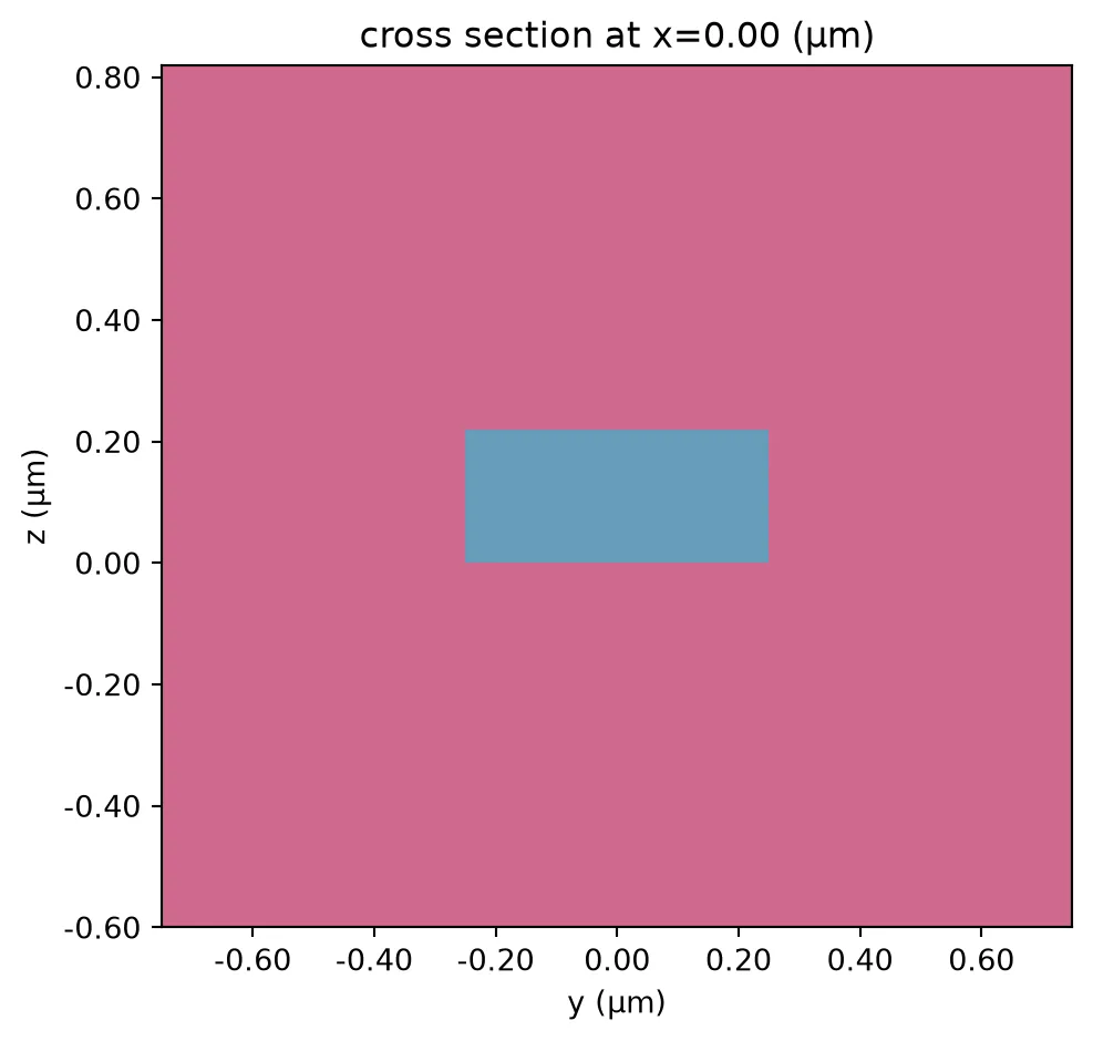
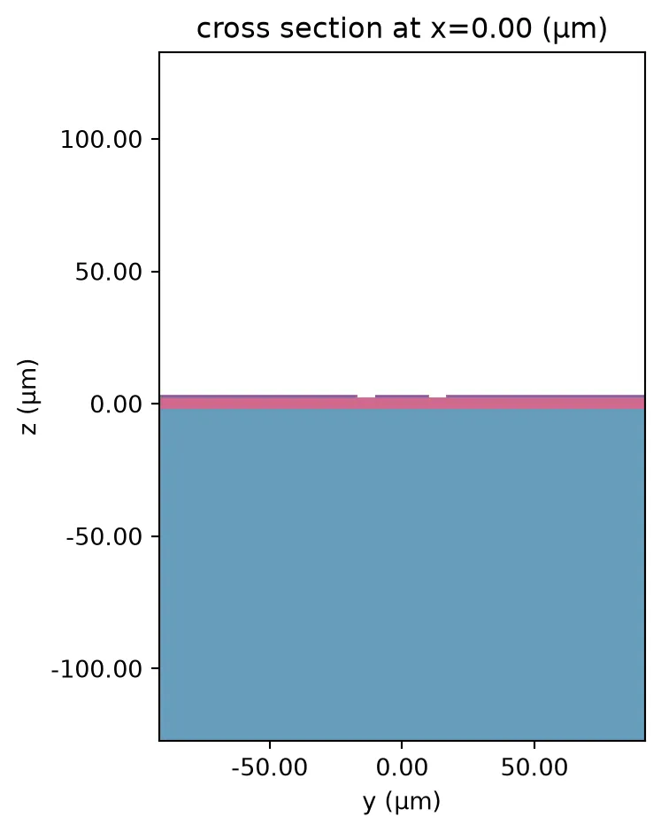
The modulator will use a co-planar waveguide (CPW) for the RF signal, so we also need to create an appropriate specification for that. We will use the cpw_spec utility to generate the specification with default parameters.
cpw_spec = pf.cpw_spec("M2_router", signal_width=20, gap=7, ground_width=75)tech.add_port("CPW", cpw_spec)
_ = pf.tidy3d_plot(cpw_spec)
14:31:34 -03 WARNING: RF simulations and functionality will require new license requirements in an upcoming release. All RF-specific classes are now available within the sub-package 'tidy3d.rf'. - Contains a 'LossyMetalMedium'.
MZM design
Section titled “MZM design”The main component in the modulator is a phase shifter. We create this, and all other components, as a parametric component, so that we can use caching, updates and store parametric arguments for free, in case we need them later.
@pf.parametric_componentdef phase_shifter(    *,    length=3000,    rib_width=7,    taper_length=10,    i_width=0.15,    p_width=1.75,    pp_width=1.7,    p_contact=1.0,    pad_size=100,    pad_distance=200,    pad_separation=150,):    strip = pf.config.default_kwargs["port_spec"]
    rib = strip.copy()    rib.description = "Phase shifter internal"    rib.width = rib_width - 2 * pf.config.tolerance    rib.path_profiles = rib.path_profiles + [(rib_width, 0, "Si Slab")]
    # Keep the vanishing slab at least 100 nm wide at the strip end    taper = pf.parametric.transition(        port_spec1=strip, port_spec2=rib, length=taper_length, min_width=0.1    )
    straight = pf.parametric.straight(port_spec=rib, length=length)
    c = pf.Component()
    # Taper in, rib section, and the same taper reversed on the way out    refs = pf.reference_chain({"taper": taper, "rib": straight}, "taper - rib - P1:taper")    c.add(*refs)
    c.add_port([refs[0]["P0"], refs[-1]["P0"]])
    doping_regions = [        # start y, width, layer        (rib_width / 2 - p_contact, p_contact, "Si"),        (i_width / 2, p_width, "Si n"),        (i_width / 2 + p_width, pp_width, "Si n++"),    ]    for y, width, layer in doping_regions:        straight.add(            layer,            pf.Rectangle(corner1=(0, y), size=(length, width)),            pf.Rectangle(corner2=(length, -y), size=(length, width)),        )
    # Add CPW    w1, off1, _ = cpw_spec.path_profiles["gnd1"]    w0, off0, _ = cpw_spec.path_profiles["signal"]    offset = (w0 / 2 + off1 - w1 / 2) / 2    cpw = pf.Reference(        pf.parametric.straight(port_spec=cpw_spec, length=length + 2 * taper_length),        (0, -offset),    )    c.add(cpw)
    # Add terminals    c.add_terminal(        {            f"{name}:{side}": pf.Terminal(                "M2_router",                pf.Rectangle(center=(x, y - offset), size=(pad_size, pad_size)),            )            for x, side in [                (-pad_distance - pad_size / 2, "in"),                (length + 2 * taper_length + pad_distance + pad_size / 2, "out"),            ]            for y, name in [                (-pad_separation, "gnd0"),                (0, "signal"),                (pad_separation, "gnd1"),            ]        }    )
    for p, side in [("E0", "in"), ("E1", "out")]:        for name in ("gnd0", "signal", "gnd1"):            c.add(                pf.parametric.route_taper(                    terminal1=c[f"{name}:{side}"], terminal2=cpw[p].terminals(name)                )            )
    # Add integrated termination    c.add(        "M1_heater",        pf.envelope([c["gnd0:in"].structure, c["gnd1:in"].structure], use_box=True),    )
    c.add_model(pf.CircuitModel(), "Circuit")
    return c
ps = phase_shifter()viewer(ps);fill:%23221f20;font-weight:bold;font-size:30.480000px;}.terminal{fill:none;stroke:%23805080;stroke-width:3.810000;}.dashed{stroke-dasharray:19.050000,11.430000;}.port{fill:none;stroke:%23805080;stroke-width:7.620000;}.virtual-connection{fill:none;stroke:%23907090;stroke-width:5.715000;}.layer_31_0{stroke:%238c78ef;fill:url(%23pat-layer_31_0);fill-opacity:0.492;}.label_31_0{fill:%238c78ef;}.layer_33_0{stroke:%238c78ef;fill:url(%23pat-layer_33_0);fill-opacity:0.492;}.label_33_0{fill:%238c78ef;}.layer_102_0{stroke:%238c78ef;fill:url(%23pat-layer_102_0);fill-opacity:0.492;}.label_102_0{fill:%238c78ef;}.layer_110_0{stroke:%238c78ef;fill:url(%23pat-layer_110_0);fill-opacity:0.492;}.label_110_0{fill:%238c78ef;}.layer_189_0{stroke:%23000000;fill:none;}.label_189_0{fill:%23000000;}.layer_201_0{stroke:%2300ee00;fill:url(%23pat-layer_201_0);fill-opacity:0.492;}.label_201_0{fill:%2300ee00;}.layer_401_0{stroke:%236a8ad2;fill:url(%23pat-layer_401_0);fill-opacity:0.492;}.label_401_0{fill:%236a8ad2;}.layer_202_0{stroke:%23007600;fill:url(%23pat-layer_202_0);fill-opacity:0.492;}.label_202_0{fill:%23007600;}.layer_68_0{stroke:%23008000;fill:url(%23pat-layer_68_0);fill-opacity:0.492;}.label_68_0{fill:%23008000;}.layer_5_0{stroke:%236a8ad2;fill:url(%23pat-layer_5_0);fill-opacity:0.492;}.label_5_0{fill:%236a8ad2;}.layer_998_0{stroke:%23000000;fill:none;}.label_998_0{fill:%23000000;}.layer_312_1{stroke:%2300b8b8;fill:url(%23pat-layer_312_1);fill-opacity:0.492;}.label_312_1{fill:%2300b8b8;}.layer_312_0{stroke:%2300b8b8;fill:url(%23pat-layer_312_0);fill-opacity:0.492;}.label_312_0{fill:%2300b8b8;}.layer_402_0{stroke:%23ff0000;fill:url(%23pat-layer_402_0);fill-opacity:0.492;}.label_402_0{fill:%23ff0000;}.layer_401_4{stroke:%236a8ad2;fill:url(%23pat-layer_401_4);fill-opacity:0.492;}.label_401_4{fill:%236a8ad2;}.layer_389_0{stroke:%23ff00ff;fill:url(%23pat-layer_389_0);fill-opacity:0.492;}.label_389_0{fill:%23ff00ff;}.layer_402_1{stroke:%23ff0000;fill:url(%23pat-layer_402_1);fill-opacity:0.492;}.label_402_1{fill:%23ff0000;}.layer_350_1{stroke:%23697a00;fill:url(%23pat-layer_350_1);fill-opacity:0.492;}.label_350_1{fill:%23697a00;}.layer_401_1{stroke:%236a8ad2;fill:url(%23pat-layer_401_1);fill-opacity:0.492;}.label_401_1{fill:%236a8ad2;}.layer_313_2{stroke:%2301d95b;fill:url(%23pat-layer_313_2);fill-opacity:0.492;}.label_313_2{fill:%2301d95b;}.layer_313_1{stroke:%2301d95b;fill:url(%23pat-layer_313_1);fill-opacity:0.492;}.label_313_1{fill:%2301d95b;}.layer_313_0{stroke:%2301d95b;fill:url(%23pat-layer_313_0);fill-opacity:0.492;}.label_313_0{fill:%2301d95b;}.layer_400_0{stroke:%23a96868;fill:url(%23pat-layer_400_0);fill-opacity:0.492;}.label_400_0{fill:%23a96868;}.layer_312_3{stroke:%2300b8b8;fill:url(%23pat-layer_312_3);fill-opacity:0.492;}.label_312_3{fill:%2300b8b8;}.layer_389_1{stroke:%23ff00ff;fill:url(%23pat-layer_389_1);fill-opacity:0.492;}.label_389_1{fill:%23ff00ff;}.layer_401_3{stroke:%236a8ad2;fill:url(%23pat-layer_401_3);fill-opacity:0.492;}.label_401_3{fill:%236a8ad2;}.layer_403_2{stroke:%23500080;fill:url(%23pat-layer_403_2);fill-opacity:0.492;}.label_403_2{fill:%23500080;}.layer_403_3{stroke:%23500080;fill:url(%23pat-layer_403_3);fill-opacity:0.492;}.label_403_3{fill:%23500080;}.layer_403_1{stroke:%23500080;fill:url(%23pat-layer_403_1);fill-opacity:0.492;}.label_403_1{fill:%23500080;}.layer_403_0{stroke:%23500080;fill:url(%23pat-layer_403_0);fill-opacity:0.492;}.label_403_0{fill:%23500080;}.layer_311_1{stroke:%23ac6c56;fill:url(%23pat-layer_311_1);fill-opacity:0.492;}.label_311_1{fill:%23ac6c56;}.layer_311_0{stroke:%23ac6c56;fill:url(%23pat-layer_311_0);fill-opacity:0.492;}.label_311_0{fill:%23ac6c56;}.layer_301_1{stroke:%23800057;fill:url(%23pat-layer_301_1);fill-opacity:0.492;}.label_301_1{fill:%23800057;}.layer_301_0{stroke:%23800057;fill:url(%23pat-layer_301_0);fill-opacity:0.492;}.label_301_0{fill:%23800057;}.layer_305_1{stroke:%23808080;fill:url(%23pat-layer_305_1);fill-opacity:0.492;}.label_305_1{fill:%23808080;}.layer_305_0{stroke:%23808080;fill:url(%23pat-layer_305_0);fill-opacity:0.492;}.label_305_0{fill:%23808080;}.layer_999_0{stroke:%230000ff;fill:url(%23pat-layer_999_0);fill-opacity:0.492;}.label_999_0{fill:%230000ff;}.layer_81_0{stroke:%23808080;fill:url(%23pat-layer_81_0);fill-opacity:0.492;}.label_81_0{fill:%23808080;}.layer_290_0{stroke:%23a46eda;fill:none;}.label_290_0{fill:%23a46eda;}.layer_205_0{stroke:%2349b203;fill:url(%23pat-layer_205_0);fill-opacity:0.492;}.label_205_0{fill:%2349b203;}.layer_11_0{stroke:%230000ff;fill:url(%23pat-layer_11_0);fill-opacity:0.492;}.label_11_0{fill:%230000ff;}.layer_12_0{stroke:%23a57b00;fill:url(%23pat-layer_12_0);fill-opacity:0.492;}.label_12_0{fill:%23a57b00;}.layer_13_0{stroke:%23800057;fill:url(%23pat-layer_13_0);fill-opacity:0.492;}.label_13_0{fill:%23800057;}.layer_6_0{stroke:%23ff0000;fill:url(%23pat-layer_6_0);fill-opacity:0.492;}.label_6_0{fill:%23ff0000;}.layer_1_10{stroke:%23c96585;fill:url(%23pat-layer_1_10);fill-opacity:0.492;}.label_1_10{fill:%23c96585;}.layer_1_11{stroke:%23800000;fill:url(%23pat-layer_1_11);fill-opacity:0.492;}.label_1_11{fill:%23800000;}.layer_200_0{stroke:%23ff0000;fill:url(%23pat-layer_200_0);fill-opacity:0.492;}.label_200_0{fill:%23ff0000;}.layer_1_0{stroke:%23c96585;fill:url(%23pat-layer_1_0);fill-opacity:0.492;}.label_1_0{fill:%23c96585;}.layer_2_0{stroke:%23a46eda;fill:url(%23pat-layer_2_0);fill-opacity:0.492;}.label_2_0{fill:%23a46eda;}.layer_20_0{stroke:%2353793d;fill:url(%23pat-layer_20_0);fill-opacity:0.492;}.label_20_0{fill:%2353793d;}.layer_22_0{stroke:%23ec7600;fill:url(%23pat-layer_22_0);fill-opacity:0.492;}.label_22_0{fill:%23ec7600;}.layer_24_0{stroke:%2300b8b8;fill:url(%23pat-layer_24_0);fill-opacity:0.492;}.label_24_0{fill:%2300b8b8;}.layer_21_0{stroke:%23736264;fill:url(%23pat-layer_21_0);fill-opacity:0.492;}.label_21_0{fill:%23736264;}.layer_23_0{stroke:%23697a00;fill:url(%23pat-layer_23_0);fill-opacity:0.492;}.label_23_0{fill:%23697a00;}.layer_25_0{stroke:%23008000;fill:url(%23pat-layer_25_0);fill-opacity:0.492;}.label_25_0{fill:%23008000;}.layer_350_0{stroke:%23697a00;fill:url(%23pat-layer_350_0);fill-opacity:0.492;}.label_350_0{fill:%23697a00;}.layer_10_0{stroke:%23000000;fill:none;}.label_10_0{fill:%23000000;}.layer_203_0{stroke:%23008000;fill:url(%23pat-layer_203_0);fill-opacity:0.492;}.label_203_0{fill:%23008000;}.layer_40_0{stroke:%230000ff;fill:url(%23pat-layer_40_0);fill-opacity:0.492;}.label_40_0{fill:%230000ff;}.layer_401_2{stroke:%236a8ad2;fill:url(%23pat-layer_401_2);fill-opacity:0.492;}.label_401_2{fill:%236a8ad2;}.layer_301_2{stroke:%23800057;fill:url(%23pat-layer_301_2);fill-opacity:0.492;}.label_301_2{fill:%23800057;}</style><defs><path id=%22port-symbol%22 class=%22port%22 d=%22M 0,-15.240000 L 22.860000,0 0,15.240000%22 /><path id=%22ref-port-symbol%22 class=%22port%22 style=%22stroke-opacity:0.33;%22 d=%22M 0,-11.430000 C 15.240000,-11.430000 15.240000,11.430000 0,11.430000%22 /><circle id=%22port-bend-symbol%22 style=%22stroke-width:0;stroke:none;fill:%23805080;fill-opacity:1;%22 cx=%220%22 cy=%220%22 r=%226.858000%22 /><circle id=%22connection-symbol%22 style=%22stroke-width:0;stroke:none;fill:%23907090;fill-opacity:1;%22 cx=%220%22 cy=%220%22 r=%228.001000%22 /><pattern id=%22pat-layer_31_0%22 patternUnits=%22userSpaceOnUse%22 width=%2219.050000%22 height=%2219.050000%22 patternTransform=%22translate(14.567647,18.047368)%22><line x1=%220%22 y1=%220%22 x2=%2219.050000%22 y2=%2219.050000%22 style=%22stroke:%238c78ef;stroke-width:1.905000%22 /><line x1=%22-9.525000%22 y1=%229.525000%22 x2=%229.525000%22 y2=%2228.575000%22 style=%22stroke:%238c78ef;stroke-width:1.905000%22 /><line x1=%229.525000%22 y1=%22-9.525000%22 x2=%2228.575000%22 y2=%229.525000%22 style=%22stroke:%238c78ef;stroke-width:1.905000%22 /></pattern><pattern id=%22pat-layer_33_0%22 patternUnits=%22userSpaceOnUse%22 width=%2219.050000%22 height=%2219.050000%22 patternTransform=%22translate(11.205882,2.005263)%22><line x1=%220%22 y1=%220%22 x2=%2219.050000%22 y2=%2219.050000%22 style=%22stroke:%238c78ef;stroke-width:1.905000%22 /><line x1=%22-9.525000%22 y1=%229.525000%22 x2=%229.525000%22 y2=%2228.575000%22 style=%22stroke:%238c78ef;stroke-width:1.905000%22 /><line x1=%229.525000%22 y1=%22-9.525000%22 x2=%2228.575000%22 y2=%229.525000%22 style=%22stroke:%238c78ef;stroke-width:1.905000%22 /></pattern><pattern id=%22pat-layer_102_0%22 patternUnits=%22userSpaceOnUse%22 width=%2219.050000%22 height=%2219.050000%22 patternTransform=%22translate(0.000000,1.002632)%22><line x1=%220%22 y1=%220%22 x2=%2219.050000%22 y2=%2219.050000%22 style=%22stroke:%238c78ef;stroke-width:1.905000%22 /><line x1=%22-9.525000%22 y1=%229.525000%22 x2=%229.525000%22 y2=%2228.575000%22 style=%22stroke:%238c78ef;stroke-width:1.905000%22 /><line x1=%229.525000%22 y1=%22-9.525000%22 x2=%2228.575000%22 y2=%229.525000%22 style=%22stroke:%238c78ef;stroke-width:1.905000%22 /></pattern><pattern id=%22pat-layer_110_0%22 patternUnits=%22userSpaceOnUse%22 width=%2219.050000%22 height=%2219.050000%22 patternTransform=%22translate(5.602941,13.034211)%22><line x1=%220%22 y1=%220%22 x2=%2219.050000%22 y2=%2219.050000%22 style=%22stroke:%238c78ef;stroke-width:1.905000%22 /><line x1=%22-9.525000%22 y1=%229.525000%22 x2=%229.525000%22 y2=%2228.575000%22 style=%22stroke:%238c78ef;stroke-width:1.905000%22 /><line x1=%229.525000%22 y1=%22-9.525000%22 x2=%2228.575000%22 y2=%229.525000%22 style=%22stroke:%238c78ef;stroke-width:1.905000%22 /></pattern><pattern id=%22pat-layer_201_0%22 patternUnits=%22userSpaceOnUse%22 width=%2219.050000%22 height=%2219.050000%22 patternTransform=%22translate(14.567647,7.018421)%22><circle cx=%229.525000%22 cy=%229.525000%22 r=%221.905000%22 style=%22stroke:none;fill:%2300ee00;fill-opacity:1.0%22 /></pattern><pattern id=%22pat-layer_401_0%22 patternUnits=%22userSpaceOnUse%22 width=%2211.430000%22 height=%2211.430000%22 patternTransform=%22translate(1.344706,1.804737)%22><line x1=%220%22 y1=%220%22 x2=%2211.430000%22 y2=%2211.430000%22 style=%22stroke:%236a8ad2;stroke-width:1.905000%22 /><line x1=%22-5.715000%22 y1=%225.715000%22 x2=%225.715000%22 y2=%2217.145000%22 style=%22stroke:%236a8ad2;stroke-width:1.905000%22 /><line x1=%225.715000%22 y1=%22-5.715000%22 x2=%2217.145000%22 y2=%225.715000%22 style=%22stroke:%236a8ad2;stroke-width:1.905000%22 /><line x1=%2211.430000%22 y1=%220%22 x2=%220%22 y2=%2211.430000%22 style=%22stroke:%236a8ad2;stroke-width:1.905000%22 /><line x1=%2217.145000%22 y1=%225.715000%22 x2=%225.715000%22 y2=%2217.145000%22 style=%22stroke:%236a8ad2;stroke-width:1.905000%22 /><line x1=%225.715000%22 y1=%22-5.715000%22 x2=%22-5.715000%22 y2=%225.715000%22 style=%22stroke:%236a8ad2;stroke-width:1.905000%22 /></pattern><pattern id=%22pat-layer_202_0%22 patternUnits=%22userSpaceOnUse%22 width=%2211.430000%22 height=%2211.430000%22 patternTransform=%22translate(2.017059,10.828421)%22><circle cx=%225.715000%22 cy=%225.715000%22 r=%221.905000%22 style=%22stroke:none;fill:%23007600;fill-opacity:1.0%22 /></pattern><pattern id=%22pat-layer_68_0%22 patternUnits=%22userSpaceOnUse%22 width=%2219.050000%22 height=%2219.050000%22 patternTransform=%22translate(0.000000,7.018421)%22><circle cx=%229.525000%22 cy=%229.525000%22 r=%221.905000%22 style=%22stroke:none;fill:%23008000;fill-opacity:1.0%22 /></pattern><pattern id=%22pat-layer_5_0%22 patternUnits=%22userSpaceOnUse%22 width=%2211.430000%22 height=%2211.430000%22 patternTransform=%22translate(0.672353,10.226842)%22><line x1=%225.715000%22 y1=%220%22 x2=%225.715000%22 y2=%2211.430000%22 style=%22stroke:%236a8ad2;stroke-width:1.905000%22 /></pattern><pattern id=%22pat-layer_312_1%22 patternUnits=%22userSpaceOnUse%22 width=%2211.430000%22 height=%2211.430000%22 patternTransform=%22translate(2.689412,9.023684)%22><line x1=%220%22 y1=%220%22 x2=%2211.430000%22 y2=%2211.430000%22 style=%22stroke:%2300b8b8;stroke-width:1.905000%22 /><line x1=%22-5.715000%22 y1=%225.715000%22 x2=%225.715000%22 y2=%2217.145000%22 style=%22stroke:%2300b8b8;stroke-width:1.905000%22 /><line x1=%225.715000%22 y1=%22-5.715000%22 x2=%2217.145000%22 y2=%225.715000%22 style=%22stroke:%2300b8b8;stroke-width:1.905000%22 /></pattern><pattern id=%22pat-layer_312_0%22 patternUnits=%22userSpaceOnUse%22 width=%2219.050000%22 height=%2219.050000%22 patternTransform=%22translate(8.964706,12.031579)%22><line x1=%229.525000%22 y1=%220%22 x2=%229.525000%22 y2=%2219.050000%22 style=%22stroke:%2300b8b8;stroke-width:1.905000%22 /></pattern><pattern id=%22pat-layer_402_0%22 patternUnits=%22userSpaceOnUse%22 width=%2219.050000%22 height=%2219.050000%22 patternTransform=%22translate(10.085294,14.036842)%22><line x1=%229.525000%22 y1=%220%22 x2=%229.525000%22 y2=%2219.050000%22 style=%22stroke:%23ff0000;stroke-width:1.905000%22 /><line x1=%220%22 y1=%229.525000%22 x2=%2219.050000%22 y2=%229.525000%22 style=%22stroke:%23ff0000;stroke-width:1.905000%22 /></pattern><pattern id=%22pat-layer_401_4%22 patternUnits=%22userSpaceOnUse%22 width=%2211.430000%22 height=%2211.430000%22 patternTransform=%22translate(2.017059,9.023684)%22><line x1=%225.715000%22 y1=%220%22 x2=%225.715000%22 y2=%2211.430000%22 style=%22stroke:%236a8ad2;stroke-width:1.905000%22 /></pattern><pattern id=%22pat-layer_389_0%22 patternUnits=%22userSpaceOnUse%22 width=%2211.430000%22 height=%2211.430000%22 patternTransform=%22translate(2.017059,2.406316)%22><line x1=%225.715000%22 y1=%220%22 x2=%225.715000%22 y2=%2211.430000%22 style=%22stroke:%23ff00ff;stroke-width:1.905000%22 /><line x1=%220%22 y1=%225.715000%22 x2=%2211.430000%22 y2=%225.715000%22 style=%22stroke:%23ff00ff;stroke-width:1.905000%22 /></pattern><pattern id=%22pat-layer_402_1%22 patternUnits=%22userSpaceOnUse%22 width=%2211.430000%22 height=%2211.430000%22 patternTransform=%22translate(3.361765,10.226842)%22><line x1=%220%22 y1=%220%22 x2=%2211.430000%22 y2=%2211.430000%22 style=%22stroke:%23ff0000;stroke-width:1.905000%22 /><line x1=%22-5.715000%22 y1=%225.715000%22 x2=%225.715000%22 y2=%2217.145000%22 style=%22stroke:%23ff0000;stroke-width:1.905000%22 /><line x1=%225.715000%22 y1=%22-5.715000%22 x2=%2217.145000%22 y2=%225.715000%22 style=%22stroke:%23ff0000;stroke-width:1.905000%22 /><line x1=%2211.430000%22 y1=%220%22 x2=%220%22 y2=%2211.430000%22 style=%22stroke:%23ff0000;stroke-width:1.905000%22 /><line x1=%2217.145000%22 y1=%225.715000%22 x2=%225.715000%22 y2=%2217.145000%22 style=%22stroke:%23ff0000;stroke-width:1.905000%22 /><line x1=%225.715000%22 y1=%22-5.715000%22 x2=%22-5.715000%22 y2=%225.715000%22 style=%22stroke:%23ff0000;stroke-width:1.905000%22 /></pattern><pattern id=%22pat-layer_350_1%22 patternUnits=%22userSpaceOnUse%22 width=%2211.430000%22 height=%2211.430000%22 patternTransform=%22translate(10.085294,9.023684)%22><circle cx=%225.715000%22 cy=%225.715000%22 r=%221.905000%22 style=%22stroke:none;fill:%23697a00;fill-opacity:1.0%22 /></pattern><pattern id=%22pat-layer_401_1%22 patternUnits=%22userSpaceOnUse%22 width=%2219.050000%22 height=%2219.050000%22 patternTransform=%22translate(16.808824,6.015789)%22><line x1=%220%22 y1=%220%22 x2=%2219.050000%22 y2=%2219.050000%22 style=%22stroke:%236a8ad2;stroke-width:1.905000%22 /><line x1=%22-9.525000%22 y1=%229.525000%22 x2=%229.525000%22 y2=%2228.575000%22 style=%22stroke:%236a8ad2;stroke-width:1.905000%22 /><line x1=%229.525000%22 y1=%22-9.525000%22 x2=%2228.575000%22 y2=%229.525000%22 style=%22stroke:%236a8ad2;stroke-width:1.905000%22 /><line x1=%2219.050000%22 y1=%220%22 x2=%220%22 y2=%2219.050000%22 style=%22stroke:%236a8ad2;stroke-width:1.905000%22 /><line x1=%2228.575000%22 y1=%229.525000%22 x2=%229.525000%22 y2=%2228.575000%22 style=%22stroke:%236a8ad2;stroke-width:1.905000%22 /><line x1=%229.525000%22 y1=%22-9.525000%22 x2=%22-9.525000%22 y2=%229.525000%22 style=%22stroke:%236a8ad2;stroke-width:1.905000%22 /></pattern><pattern id=%22pat-layer_313_2%22 patternUnits=%22userSpaceOnUse%22 width=%2211.430000%22 height=%2211.430000%22 patternTransform=%22translate(4.706471,6.015789)%22><line x1=%220%22 y1=%220%22 x2=%2211.430000%22 y2=%2211.430000%22 style=%22stroke:%2301d95b;stroke-width:1.905000%22 /><line x1=%22-5.715000%22 y1=%225.715000%22 x2=%225.715000%22 y2=%2217.145000%22 style=%22stroke:%2301d95b;stroke-width:1.905000%22 /><line x1=%225.715000%22 y1=%22-5.715000%22 x2=%2217.145000%22 y2=%225.715000%22 style=%22stroke:%2301d95b;stroke-width:1.905000%22 /></pattern><pattern id=%22pat-layer_313_1%22 patternUnits=%22userSpaceOnUse%22 width=%2219.050000%22 height=%2219.050000%22 patternTransform=%22translate(12.326471,7.018421)%22><line x1=%229.525000%22 y1=%220%22 x2=%229.525000%22 y2=%2219.050000%22 style=%22stroke:%2301d95b;stroke-width:1.905000%22 /></pattern><pattern id=%22pat-layer_313_0%22 patternUnits=%22userSpaceOnUse%22 width=%2211.430000%22 height=%2211.430000%22 patternTransform=%22translate(10.085294,2.406316)%22><line x1=%225.715000%22 y1=%220%22 x2=%225.715000%22 y2=%2211.430000%22 style=%22stroke:%2301d95b;stroke-width:1.905000%22 /></pattern><pattern id=%22pat-layer_400_0%22 patternUnits=%22userSpaceOnUse%22 width=%2219.050000%22 height=%2219.050000%22 patternTransform=%22translate(13.447059,11.028947)%22><line x1=%220%22 y1=%220%22 x2=%2219.050000%22 y2=%2219.050000%22 style=%22stroke:%23a96868;stroke-width:1.905000%22 /><line x1=%22-9.525000%22 y1=%229.525000%22 x2=%229.525000%22 y2=%2228.575000%22 style=%22stroke:%23a96868;stroke-width:1.905000%22 /><line x1=%229.525000%22 y1=%22-9.525000%22 x2=%2228.575000%22 y2=%229.525000%22 style=%22stroke:%23a96868;stroke-width:1.905000%22 /><line x1=%2219.050000%22 y1=%220%22 x2=%220%22 y2=%2219.050000%22 style=%22stroke:%23a96868;stroke-width:1.905000%22 /><line x1=%2228.575000%22 y1=%229.525000%22 x2=%229.525000%22 y2=%2228.575000%22 style=%22stroke:%23a96868;stroke-width:1.905000%22 /><line x1=%229.525000%22 y1=%22-9.525000%22 x2=%22-9.525000%22 y2=%229.525000%22 style=%22stroke:%23a96868;stroke-width:1.905000%22 /></pattern><pattern id=%22pat-layer_312_3%22 patternUnits=%22userSpaceOnUse%22 width=%2211.430000%22 height=%2211.430000%22 patternTransform=%22translate(8.740588,1.203158)%22><line x1=%2211.430000%22 y1=%220%22 x2=%220%22 y2=%2211.430000%22 style=%22stroke:%2300b8b8;stroke-width:1.905000%22 /><line x1=%2217.145000%22 y1=%225.715000%22 x2=%225.715000%22 y2=%2217.145000%22 style=%22stroke:%2300b8b8;stroke-width:1.905000%22 /><line x1=%225.715000%22 y1=%22-5.715000%22 x2=%22-5.715000%22 y2=%225.715000%22 style=%22stroke:%2300b8b8;stroke-width:1.905000%22 /></pattern><pattern id=%22pat-layer_389_1%22 patternUnits=%22userSpaceOnUse%22 width=%2219.050000%22 height=%2219.050000%22 patternTransform=%22translate(17.929412,7.018421)%22><line x1=%229.525000%22 y1=%220%22 x2=%229.525000%22 y2=%2219.050000%22 style=%22stroke:%23ff00ff;stroke-width:1.905000%22 /><line x1=%220%22 y1=%229.525000%22 x2=%2219.050000%22 y2=%229.525000%22 style=%22stroke:%23ff00ff;stroke-width:1.905000%22 /></pattern><pattern id=%22pat-layer_401_3%22 patternUnits=%22userSpaceOnUse%22 width=%2219.050000%22 height=%2219.050000%22 patternTransform=%22translate(7.844118,12.031579)%22><line x1=%220%22 y1=%229.525000%22 x2=%2219.050000%22 y2=%229.525000%22 style=%22stroke:%236a8ad2;stroke-width:1.905000%22 /></pattern><pattern id=%22pat-layer_403_2%22 patternUnits=%22userSpaceOnUse%22 width=%2211.430000%22 height=%2211.430000%22 patternTransform=%22translate(5.378824,7.218947)%22><line x1=%220%22 y1=%220%22 x2=%2211.430000%22 y2=%2211.430000%22 style=%22stroke:%23500080;stroke-width:1.905000%22 /><line x1=%22-5.715000%22 y1=%225.715000%22 x2=%225.715000%22 y2=%2217.145000%22 style=%22stroke:%23500080;stroke-width:1.905000%22 /><line x1=%225.715000%22 y1=%22-5.715000%22 x2=%2217.145000%22 y2=%225.715000%22 style=%22stroke:%23500080;stroke-width:1.905000%22 /><line x1=%2211.430000%22 y1=%220%22 x2=%220%22 y2=%2211.430000%22 style=%22stroke:%23500080;stroke-width:1.905000%22 /><line x1=%2217.145000%22 y1=%225.715000%22 x2=%225.715000%22 y2=%2217.145000%22 style=%22stroke:%23500080;stroke-width:1.905000%22 /><line x1=%225.715000%22 y1=%22-5.715000%22 x2=%22-5.715000%22 y2=%225.715000%22 style=%22stroke:%23500080;stroke-width:1.905000%22 /></pattern><pattern id=%22pat-layer_403_3%22 patternUnits=%22userSpaceOnUse%22 width=%2219.050000%22 height=%2219.050000%22 patternTransform=%22translate(4.482353,15.039474)%22><line x1=%220%22 y1=%220%22 x2=%2219.050000%22 y2=%2219.050000%22 style=%22stroke:%23500080;stroke-width:1.905000%22 /><line x1=%22-9.525000%22 y1=%229.525000%22 x2=%229.525000%22 y2=%2228.575000%22 style=%22stroke:%23500080;stroke-width:1.905000%22 /><line x1=%229.525000%22 y1=%22-9.525000%22 x2=%2228.575000%22 y2=%229.525000%22 style=%22stroke:%23500080;stroke-width:1.905000%22 /><line x1=%2219.050000%22 y1=%220%22 x2=%220%22 y2=%2219.050000%22 style=%22stroke:%23500080;stroke-width:1.905000%22 /><line x1=%2228.575000%22 y1=%229.525000%22 x2=%229.525000%22 y2=%2228.575000%22 style=%22stroke:%23500080;stroke-width:1.905000%22 /><line x1=%229.525000%22 y1=%22-9.525000%22 x2=%22-9.525000%22 y2=%229.525000%22 style=%22stroke:%23500080;stroke-width:1.905000%22 /></pattern><pattern id=%22pat-layer_403_1%22 patternUnits=%22userSpaceOnUse%22 width=%2219.050000%22 height=%2219.050000%22 patternTransform=%22translate(13.447059,9.023684)%22><line x1=%229.525000%22 y1=%220%22 x2=%229.525000%22 y2=%2219.050000%22 style=%22stroke:%23500080;stroke-width:1.905000%22 /><line x1=%220%22 y1=%229.525000%22 x2=%2219.050000%22 y2=%229.525000%22 style=%22stroke:%23500080;stroke-width:1.905000%22 /></pattern><pattern id=%22pat-layer_403_0%22 patternUnits=%22userSpaceOnUse%22 width=%2211.430000%22 height=%2211.430000%22 patternTransform=%22translate(10.757647,3.609474)%22><line x1=%225.715000%22 y1=%220%22 x2=%225.715000%22 y2=%2211.430000%22 style=%22stroke:%23500080;stroke-width:1.905000%22 /><line x1=%220%22 y1=%225.715000%22 x2=%2211.430000%22 y2=%225.715000%22 style=%22stroke:%23500080;stroke-width:1.905000%22 /></pattern><pattern id=%22pat-layer_311_1%22 patternUnits=%22userSpaceOnUse%22 width=%2219.050000%22 height=%2219.050000%22 patternTransform=%22translate(15.688235,4.010526)%22><line x1=%220%22 y1=%220%22 x2=%2219.050000%22 y2=%2219.050000%22 style=%22stroke:%23ac6c56;stroke-width:1.905000%22 /><line x1=%22-9.525000%22 y1=%229.525000%22 x2=%229.525000%22 y2=%2228.575000%22 style=%22stroke:%23ac6c56;stroke-width:1.905000%22 /><line x1=%229.525000%22 y1=%22-9.525000%22 x2=%2228.575000%22 y2=%229.525000%22 style=%22stroke:%23ac6c56;stroke-width:1.905000%22 /></pattern><pattern id=%22pat-layer_311_0%22 patternUnits=%22userSpaceOnUse%22 width=%2211.430000%22 height=%2211.430000%22 patternTransform=%22translate(0.672353,0.601579)%22><line x1=%220%22 y1=%220%22 x2=%2211.430000%22 y2=%2211.430000%22 style=%22stroke:%23ac6c56;stroke-width:1.905000%22 /><line x1=%22-5.715000%22 y1=%225.715000%22 x2=%225.715000%22 y2=%2217.145000%22 style=%22stroke:%23ac6c56;stroke-width:1.905000%22 /><line x1=%225.715000%22 y1=%22-5.715000%22 x2=%2217.145000%22 y2=%225.715000%22 style=%22stroke:%23ac6c56;stroke-width:1.905000%22 /></pattern><pattern id=%22pat-layer_301_1%22 patternUnits=%22userSpaceOnUse%22 width=%2219.050000%22 height=%2219.050000%22 patternTransform=%22translate(13.447059,8.021053)%22><line x1=%220%22 y1=%229.525000%22 x2=%2219.050000%22 y2=%229.525000%22 style=%22stroke:%23800057;stroke-width:1.905000%22 /></pattern><pattern id=%22pat-layer_301_0%22 patternUnits=%22userSpaceOnUse%22 width=%2211.430000%22 height=%2211.430000%22 patternTransform=%22translate(10.757647,3.007895)%22><line x1=%220%22 y1=%225.715000%22 x2=%2211.430000%22 y2=%225.715000%22 style=%22stroke:%23800057;stroke-width:1.905000%22 /></pattern><pattern id=%22pat-layer_305_1%22 patternUnits=%22userSpaceOnUse%22 width=%2219.050000%22 height=%2219.050000%22 patternTransform=%22translate(6.723529,14.036842)%22><line x1=%229.525000%22 y1=%220%22 x2=%229.525000%22 y2=%2219.050000%22 style=%22stroke:%23808080;stroke-width:1.905000%22 /><line x1=%220%22 y1=%229.525000%22 x2=%2219.050000%22 y2=%229.525000%22 style=%22stroke:%23808080;stroke-width:1.905000%22 /></pattern><pattern id=%22pat-layer_305_0%22 patternUnits=%22userSpaceOnUse%22 width=%2211.430000%22 height=%2211.430000%22 patternTransform=%22translate(6.723529,6.617368)%22><line x1=%225.715000%22 y1=%220%22 x2=%225.715000%22 y2=%2211.430000%22 style=%22stroke:%23808080;stroke-width:1.905000%22 /><line x1=%220%22 y1=%225.715000%22 x2=%2211.430000%22 y2=%225.715000%22 style=%22stroke:%23808080;stroke-width:1.905000%22 /></pattern><pattern id=%22pat-layer_999_0%22 patternUnits=%22userSpaceOnUse%22 width=%2211.430000%22 height=%2211.430000%22 patternTransform=%22translate(4.034118,4.211053)%22><line x1=%225.715000%22 y1=%220%22 x2=%225.715000%22 y2=%2211.430000%22 style=%22stroke:%230000ff;stroke-width:1.905000%22 /></pattern><pattern id=%22pat-layer_81_0%22 patternUnits=%22userSpaceOnUse%22 width=%2211.430000%22 height=%2211.430000%22 patternTransform=%22translate(4.034118,10.226842)%22><line x1=%225.715000%22 y1=%220%22 x2=%225.715000%22 y2=%2211.430000%22 style=%22stroke:%23808080;stroke-width:1.905000%22 /><line x1=%220%22 y1=%225.715000%22 x2=%2211.430000%22 y2=%225.715000%22 style=%22stroke:%23808080;stroke-width:1.905000%22 /></pattern><pattern id=%22pat-layer_205_0%22 patternUnits=%22userSpaceOnUse%22 width=%2211.430000%22 height=%2211.430000%22 patternTransform=%22translate(4.706471,7.820526)%22><line x1=%220%22 y1=%220%22 x2=%2211.430000%22 y2=%2211.430000%22 style=%22stroke:%2349b203;stroke-width:1.905000%22 /><line x1=%22-5.715000%22 y1=%225.715000%22 x2=%225.715000%22 y2=%2217.145000%22 style=%22stroke:%2349b203;stroke-width:1.905000%22 /><line x1=%225.715000%22 y1=%22-5.715000%22 x2=%2217.145000%22 y2=%225.715000%22 style=%22stroke:%2349b203;stroke-width:1.905000%22 /><line x1=%2211.430000%22 y1=%220%22 x2=%220%22 y2=%2211.430000%22 style=%22stroke:%2349b203;stroke-width:1.905000%22 /><line x1=%2217.145000%22 y1=%225.715000%22 x2=%225.715000%22 y2=%2217.145000%22 style=%22stroke:%2349b203;stroke-width:1.905000%22 /><line x1=%225.715000%22 y1=%22-5.715000%22 x2=%22-5.715000%22 y2=%225.715000%22 style=%22stroke:%2349b203;stroke-width:1.905000%22 /></pattern><pattern id=%22pat-layer_11_0%22 patternUnits=%22userSpaceOnUse%22 width=%2211.430000%22 height=%2211.430000%22 patternTransform=%22translate(6.051176,4.211053)%22><line x1=%2211.430000%22 y1=%220%22 x2=%220%22 y2=%2211.430000%22 style=%22stroke:%230000ff;stroke-width:1.905000%22 /><line x1=%2217.145000%22 y1=%225.715000%22 x2=%225.715000%22 y2=%2217.145000%22 style=%22stroke:%230000ff;stroke-width:1.905000%22 /><line x1=%225.715000%22 y1=%22-5.715000%22 x2=%22-5.715000%22 y2=%225.715000%22 style=%22stroke:%230000ff;stroke-width:1.905000%22 /></pattern><pattern id=%22pat-layer_12_0%22 patternUnits=%22userSpaceOnUse%22 width=%2211.430000%22 height=%2211.430000%22 patternTransform=%22translate(10.757647,10.828421)%22><line x1=%220%22 y1=%220%22 x2=%2211.430000%22 y2=%2211.430000%22 style=%22stroke:%23a57b00;stroke-width:1.905000%22 /><line x1=%22-5.715000%22 y1=%225.715000%22 x2=%225.715000%22 y2=%2217.145000%22 style=%22stroke:%23a57b00;stroke-width:1.905000%22 /><line x1=%225.715000%22 y1=%22-5.715000%22 x2=%2217.145000%22 y2=%225.715000%22 style=%22stroke:%23a57b00;stroke-width:1.905000%22 /></pattern><pattern id=%22pat-layer_13_0%22 patternUnits=%22userSpaceOnUse%22 width=%2211.430000%22 height=%2211.430000%22 patternTransform=%22translate(4.034118,6.015789)%22><line x1=%2211.430000%22 y1=%220%22 x2=%220%22 y2=%2211.430000%22 style=%22stroke:%23800057;stroke-width:1.905000%22 /><line x1=%2217.145000%22 y1=%225.715000%22 x2=%225.715000%22 y2=%2217.145000%22 style=%22stroke:%23800057;stroke-width:1.905000%22 /><line x1=%225.715000%22 y1=%22-5.715000%22 x2=%22-5.715000%22 y2=%225.715000%22 style=%22stroke:%23800057;stroke-width:1.905000%22 /></pattern><pattern id=%22pat-layer_6_0%22 patternUnits=%22userSpaceOnUse%22 width=%2219.050000%22 height=%2219.050000%22 patternTransform=%22translate(8.964706,9.023684)%22><line x1=%220%22 y1=%229.525000%22 x2=%2219.050000%22 y2=%229.525000%22 style=%22stroke:%23ff0000;stroke-width:1.905000%22 /></pattern><pattern id=%22pat-layer_1_10%22 patternUnits=%22userSpaceOnUse%22 width=%2211.430000%22 height=%2211.430000%22 patternTransform=%22translate(0.672353,1.804737)%22><line x1=%220%22 y1=%220%22 x2=%2211.430000%22 y2=%2211.430000%22 style=%22stroke:%23c96585;stroke-width:1.905000%22 /><line x1=%22-5.715000%22 y1=%225.715000%22 x2=%225.715000%22 y2=%2217.145000%22 style=%22stroke:%23c96585;stroke-width:1.905000%22 /><line x1=%225.715000%22 y1=%22-5.715000%22 x2=%2217.145000%22 y2=%225.715000%22 style=%22stroke:%23c96585;stroke-width:1.905000%22 /><line x1=%2211.430000%22 y1=%220%22 x2=%220%22 y2=%2211.430000%22 style=%22stroke:%23c96585;stroke-width:1.905000%22 /><line x1=%2217.145000%22 y1=%225.715000%22 x2=%225.715000%22 y2=%2217.145000%22 style=%22stroke:%23c96585;stroke-width:1.905000%22 /><line x1=%225.715000%22 y1=%22-5.715000%22 x2=%22-5.715000%22 y2=%225.715000%22 style=%22stroke:%23c96585;stroke-width:1.905000%22 /></pattern><pattern id=%22pat-layer_1_11%22 patternUnits=%22userSpaceOnUse%22 width=%2219.050000%22 height=%2219.050000%22 patternTransform=%22translate(15.688235,6.015789)%22><line x1=%229.525000%22 y1=%220%22 x2=%229.525000%22 y2=%2219.050000%22 style=%22stroke:%23800000;stroke-width:1.905000%22 /><line x1=%220%22 y1=%229.525000%22 x2=%2219.050000%22 y2=%229.525000%22 style=%22stroke:%23800000;stroke-width:1.905000%22 /></pattern><pattern id=%22pat-layer_200_0%22 patternUnits=%22userSpaceOnUse%22 width=%2219.050000%22 height=%2219.050000%22 patternTransform=%22translate(6.723529,15.039474)%22><line x1=%220%22 y1=%220%22 x2=%2219.050000%22 y2=%2219.050000%22 style=%22stroke:%23ff0000;stroke-width:1.905000%22 /><line x1=%22-9.525000%22 y1=%229.525000%22 x2=%229.525000%22 y2=%2228.575000%22 style=%22stroke:%23ff0000;stroke-width:1.905000%22 /><line x1=%229.525000%22 y1=%22-9.525000%22 x2=%2228.575000%22 y2=%229.525000%22 style=%22stroke:%23ff0000;stroke-width:1.905000%22 /><line x1=%2219.050000%22 y1=%220%22 x2=%220%22 y2=%2219.050000%22 style=%22stroke:%23ff0000;stroke-width:1.905000%22 /><line x1=%2228.575000%22 y1=%229.525000%22 x2=%229.525000%22 y2=%2228.575000%22 style=%22stroke:%23ff0000;stroke-width:1.905000%22 /><line x1=%229.525000%22 y1=%22-9.525000%22 x2=%22-9.525000%22 y2=%229.525000%22 style=%22stroke:%23ff0000;stroke-width:1.905000%22 /></pattern><pattern id=%22pat-layer_1_0%22 patternUnits=%22userSpaceOnUse%22 width=%2211.430000%22 height=%2211.430000%22 patternTransform=%22translate(4.706471,6.617368)%22><line x1=%2211.430000%22 y1=%220%22 x2=%220%22 y2=%2211.430000%22 style=%22stroke:%23c96585;stroke-width:1.905000%22 /><line x1=%2217.145000%22 y1=%225.715000%22 x2=%225.715000%22 y2=%2217.145000%22 style=%22stroke:%23c96585;stroke-width:1.905000%22 /><line x1=%225.715000%22 y1=%22-5.715000%22 x2=%22-5.715000%22 y2=%225.715000%22 style=%22stroke:%23c96585;stroke-width:1.905000%22 /></pattern><pattern id=%22pat-layer_2_0%22 patternUnits=%22userSpaceOnUse%22 width=%2219.050000%22 height=%2219.050000%22 patternTransform=%22translate(15.688235,3.007895)%22><line x1=%220%22 y1=%220%22 x2=%2219.050000%22 y2=%2219.050000%22 style=%22stroke:%23a46eda;stroke-width:1.905000%22 /><line x1=%22-9.525000%22 y1=%229.525000%22 x2=%229.525000%22 y2=%2228.575000%22 style=%22stroke:%23a46eda;stroke-width:1.905000%22 /><line x1=%229.525000%22 y1=%22-9.525000%22 x2=%2228.575000%22 y2=%229.525000%22 style=%22stroke:%23a46eda;stroke-width:1.905000%22 /></pattern><pattern id=%22pat-layer_20_0%22 patternUnits=%22userSpaceOnUse%22 width=%2219.050000%22 height=%2219.050000%22 patternTransform=%22translate(4.482353,11.028947)%22><line x1=%220%22 y1=%229.525000%22 x2=%2219.050000%22 y2=%229.525000%22 style=%22stroke:%2353793d;stroke-width:1.905000%22 /></pattern><pattern id=%22pat-layer_22_0%22 patternUnits=%22userSpaceOnUse%22 width=%2219.050000%22 height=%2219.050000%22 patternTransform=%22translate(1.120588,14.036842)%22><line x1=%220%22 y1=%220%22 x2=%2219.050000%22 y2=%2219.050000%22 style=%22stroke:%23ec7600;stroke-width:1.905000%22 /><line x1=%22-9.525000%22 y1=%229.525000%22 x2=%229.525000%22 y2=%2228.575000%22 style=%22stroke:%23ec7600;stroke-width:1.905000%22 /><line x1=%229.525000%22 y1=%22-9.525000%22 x2=%2228.575000%22 y2=%229.525000%22 style=%22stroke:%23ec7600;stroke-width:1.905000%22 /><line x1=%2219.050000%22 y1=%220%22 x2=%220%22 y2=%2219.050000%22 style=%22stroke:%23ec7600;stroke-width:1.905000%22 /><line x1=%2228.575000%22 y1=%229.525000%22 x2=%229.525000%22 y2=%2228.575000%22 style=%22stroke:%23ec7600;stroke-width:1.905000%22 /><line x1=%229.525000%22 y1=%22-9.525000%22 x2=%22-9.525000%22 y2=%229.525000%22 style=%22stroke:%23ec7600;stroke-width:1.905000%22 /></pattern><pattern id=%22pat-layer_24_0%22 patternUnits=%22userSpaceOnUse%22 width=%2219.050000%22 height=%2219.050000%22 patternTransform=%22translate(16.808824,17.044737)%22><line x1=%229.525000%22 y1=%220%22 x2=%229.525000%22 y2=%2219.050000%22 style=%22stroke:%2300b8b8;stroke-width:1.905000%22 /><line x1=%220%22 y1=%229.525000%22 x2=%2219.050000%22 y2=%229.525000%22 style=%22stroke:%2300b8b8;stroke-width:1.905000%22 /></pattern><pattern id=%22pat-layer_21_0%22 patternUnits=%22userSpaceOnUse%22 width=%2211.430000%22 height=%2211.430000%22 patternTransform=%22translate(7.395882,1.804737)%22><line x1=%220%22 y1=%225.715000%22 x2=%2211.430000%22 y2=%225.715000%22 style=%22stroke:%23736264;stroke-width:1.905000%22 /></pattern><pattern id=%22pat-layer_23_0%22 patternUnits=%22userSpaceOnUse%22 width=%2211.430000%22 height=%2211.430000%22 patternTransform=%22translate(5.378824,3.609474)%22><line x1=%220%22 y1=%220%22 x2=%2211.430000%22 y2=%2211.430000%22 style=%22stroke:%23697a00;stroke-width:1.905000%22 /><line x1=%22-5.715000%22 y1=%225.715000%22 x2=%225.715000%22 y2=%2217.145000%22 style=%22stroke:%23697a00;stroke-width:1.905000%22 /><line x1=%225.715000%22 y1=%22-5.715000%22 x2=%2217.145000%22 y2=%225.715000%22 style=%22stroke:%23697a00;stroke-width:1.905000%22 /><line x1=%2211.430000%22 y1=%220%22 x2=%220%22 y2=%2211.430000%22 style=%22stroke:%23697a00;stroke-width:1.905000%22 /><line x1=%2217.145000%22 y1=%225.715000%22 x2=%225.715000%22 y2=%2217.145000%22 style=%22stroke:%23697a00;stroke-width:1.905000%22 /><line x1=%225.715000%22 y1=%22-5.715000%22 x2=%22-5.715000%22 y2=%225.715000%22 style=%22stroke:%23697a00;stroke-width:1.905000%22 /></pattern><pattern id=%22pat-layer_25_0%22 patternUnits=%22userSpaceOnUse%22 width=%2211.430000%22 height=%2211.430000%22 patternTransform=%22translate(3.361765,5.414211)%22><line x1=%225.715000%22 y1=%220%22 x2=%225.715000%22 y2=%2211.430000%22 style=%22stroke:%23008000;stroke-width:1.905000%22 /><line x1=%220%22 y1=%225.715000%22 x2=%2211.430000%22 y2=%225.715000%22 style=%22stroke:%23008000;stroke-width:1.905000%22 /></pattern><pattern id=%22pat-layer_350_0%22 patternUnits=%22userSpaceOnUse%22 width=%2219.050000%22 height=%2219.050000%22 patternTransform=%22translate(2.241176,12.031579)%22><line x1=%2219.050000%22 y1=%220%22 x2=%220%22 y2=%2219.050000%22 style=%22stroke:%23697a00;stroke-width:1.905000%22 /><line x1=%2228.575000%22 y1=%229.525000%22 x2=%229.525000%22 y2=%2228.575000%22 style=%22stroke:%23697a00;stroke-width:1.905000%22 /><line x1=%229.525000%22 y1=%22-9.525000%22 x2=%22-9.525000%22 y2=%229.525000%22 style=%22stroke:%23697a00;stroke-width:1.905000%22 /></pattern><pattern id=%22pat-layer_203_0%22 patternUnits=%22userSpaceOnUse%22 width=%2219.050000%22 height=%2219.050000%22 patternTransform=%22translate(11.205882,10.026316)%22><line x1=%2219.050000%22 y1=%220%22 x2=%220%22 y2=%2219.050000%22 style=%22stroke:%23008000;stroke-width:1.905000%22 /><line x1=%2228.575000%22 y1=%229.525000%22 x2=%229.525000%22 y2=%2228.575000%22 style=%22stroke:%23008000;stroke-width:1.905000%22 /><line x1=%229.525000%22 y1=%22-9.525000%22 x2=%22-9.525000%22 y2=%229.525000%22 style=%22stroke:%23008000;stroke-width:1.905000%22 /></pattern><pattern id=%22pat-layer_40_0%22 patternUnits=%22userSpaceOnUse%22 width=%2219.050000%22 height=%2219.050000%22 patternTransform=%22translate(8.964706,3.007895)%22><circle cx=%229.525000%22 cy=%229.525000%22 r=%221.905000%22 style=%22stroke:none;fill:%230000ff;fill-opacity:1.0%22 /></pattern><pattern id=%22pat-layer_401_2%22 patternUnits=%22userSpaceOnUse%22 width=%2211.430000%22 height=%2211.430000%22 patternTransform=%22translate(7.395882,5.414211)%22><line x1=%220%22 y1=%225.715000%22 x2=%2211.430000%22 y2=%225.715000%22 style=%22stroke:%236a8ad2;stroke-width:1.905000%22 /></pattern><pattern id=%22pat-layer_301_2%22 patternUnits=%22userSpaceOnUse%22 width=%2211.430000%22 height=%2211.430000%22 patternTransform=%22translate(5.378824,6.617368)%22><line x1=%225.715000%22 y1=%220%22 x2=%225.715000%22 y2=%2211.430000%22 style=%22stroke:%23800057;stroke-width:1.905000%22 /></pattern><g id=%22C1%22 data-name=%22transition__EEK7YDANI3L7IG4J7AMIPLPBJEXPLWRN2AMRGTQK2NUDSABZUVYQ%22><path class=%22layer_1_0%22 d=%22M 0.000000,-0.250000 2.000000,-0.250000 4.000000,-0.250000 6.000000,-0.250000 8.000000,-0.250000 10.000000,-0.250000 10.000000,0.250000 8.000000,0.250000 6.000000,0.250000 4.000000,0.250000 2.000000,0.250000 0.000000,0.250000 z%22 /><path class=%22layer_2_0%22 d=%22M 0.000000,-0.050000 2.000000,-0.740000 4.000000,-1.430000 6.000000,-2.120000 8.000000,-2.810000 10.000000,-3.500000 10.000000,3.500000 8.000000,2.810000 6.000000,2.120000 4.000000,1.430000 2.000000,0.740000 0.000000,0.050000 z%22 /></g><g id=%22C2%22 data-name=%22straight__OYIDNPXIGLDUNJBFA3FHQUX3ANOVBM67U7CP4ZVPGFBYV4JY6MWQ%22><path class=%22layer_1_0%22 d=%22M 0.000000,-0.250000 3000.000000,-0.250000 3000.000000,0.250000 0.000000,0.250000 z%22 /><rect class=%22layer_1_0%22 x=%220.000000%22 y=%222.500000%22 width=%223000.000000%22 height=%221.000000%22 /><rect class=%22layer_1_0%22 x=%220.000000%22 y=%22-3.500000%22 width=%223000.000000%22 height=%221.000000%22 /><path class=%22layer_2_0%22 d=%22M 0.000000,-3.500000 3000.000000,-3.500000 3000.000000,3.500000 0.000000,3.500000 z%22 /><rect class=%22layer_20_0%22 x=%220.000000%22 y=%220.075000%22 width=%223000.000000%22 height=%221.750000%22 /><rect class=%22layer_20_0%22 x=%220.000000%22 y=%22-1.825000%22 width=%223000.000000%22 height=%221.750000%22 /><rect class=%22layer_24_0%22 x=%220.000000%22 y=%221.825000%22 width=%223000.000000%22 height=%221.700000%22 /><rect class=%22layer_24_0%22 x=%220.000000%22 y=%22-3.525000%22 width=%223000.000000%22 height=%221.700000%22 /></g><g id=%22C3%22 data-name=%22straight__B2AS62VTPVMX74SO36JQ4D2KXZI5L3VFWUHD5LKIAHVA3HQVWPHA%22><path class=%22layer_12_0%22 d=%22M 0.000000,-92.000000 3020.000000,-92.000000 3020.000000,-17.000000 0.000000,-17.000000 z%22 /><path class=%22layer_12_0%22 d=%22M 0.000000,17.000000 3020.000000,17.000000 3020.000000,92.000000 0.000000,92.000000 z%22 /><path class=%22layer_12_0%22 d=%22M 0.000000,-10.000000 3020.000000,-10.000000 3020.000000,10.000000 0.000000,10.000000 z%22 /></g><g id=%22C4%22 data-name=%22route_taper__Y7SNPRGLD4LDYKILSG5XUU676X6ONCBFH2RC4DXCPM74F5UOZGJA%22><path class=%22layer_12_0%22 d=%22M -200.000000,-113.500000 -300.000000,-113.500000 -300.000000,-213.500000 -200.000000,-213.500000 0.000000,-105.500000 0.000000,-30.500000 z%22 /><rect class=%22terminal dashed%22 x=%22-300.000000%22 y=%22-213.500000%22 width=%22100.000000%22 height=%22100.000000%22 /><rect class=%22terminal dashed%22 x=%220.000000%22 y=%22-105.500000%22 width=%220.000000%22 height=%2275.000000%22 /></g><g id=%22C5%22 data-name=%22route_taper__ZAQVA2AIPWRW7UG7T4RLWFK6U3CGJCTQJFBNC4XULRRH76JZV6QA%22><path class=%22layer_12_0%22 d=%22M -200.000000,36.500000 -300.000000,36.500000 -300.000000,-63.500000 -200.000000,-63.500000 0.000000,-23.500000 0.000000,-3.500000 z%22 /><rect class=%22terminal dashed%22 x=%22-300.000000%22 y=%22-63.500000%22 width=%22100.000000%22 height=%22100.000000%22 /><rect class=%22terminal dashed%22 x=%220.000000%22 y=%22-23.500000%22 width=%220.000000%22 height=%2220.000000%22 /></g><g id=%22C6%22 data-name=%22route_taper__BWDDP4R4PJAPVM25XZLIMHN7PQ7PIBNYVMF5W3I65ELT6ZAYP33A%22><path class=%22layer_12_0%22 d=%22M -200.000000,186.500000 -300.000000,186.500000 -300.000000,86.500000 -200.000000,86.500000 0.000000,3.500000 0.000000,78.500000 z%22 /><rect class=%22terminal dashed%22 x=%22-300.000000%22 y=%2286.500000%22 width=%22100.000000%22 height=%22100.000000%22 /><rect class=%22terminal dashed%22 x=%220.000000%22 y=%223.500000%22 width=%220.000000%22 height=%2275.000000%22 /></g><g id=%22C7%22 data-name=%22route_taper__JCQKDUD3SFWHJB7H4TYBLASDQPBY2MTZWSPK2ATX27P7UXMU3MNQ%22><path class=%22layer_12_0%22 d=%22M 3020.000000,-30.500000 3020.000000,-105.500000 3220.000000,-213.500000 3320.000000,-213.500000 3320.000000,-113.500000 3220.000000,-113.500000 z%22 /><rect class=%22terminal dashed%22 x=%223220.000000%22 y=%22-213.500000%22 width=%22100.000000%22 height=%22100.000000%22 /><rect class=%22terminal dashed%22 x=%223020.000000%22 y=%22-105.500000%22 width=%220.000000%22 height=%2275.000000%22 transform=%22translate(3020.000000 -68.000000) rotate(180.000000) translate(-3020.000000 68.000000)%22 /></g><g id=%22C8%22 data-name=%22route_taper__EUNNXKISZS6A62WTLRN75MD6WX54YSMXC7KGD32IGSHDDX5SD4BA%22><path class=%22layer_12_0%22 d=%22M 3020.000000,-3.500000 3020.000000,-23.500000 3220.000000,-63.500000 3320.000000,-63.500000 3320.000000,36.500000 3220.000000,36.500000 z%22 /><rect class=%22terminal dashed%22 x=%223220.000000%22 y=%22-63.500000%22 width=%22100.000000%22 height=%22100.000000%22 /><rect class=%22terminal dashed%22 x=%223020.000000%22 y=%22-23.500000%22 width=%220.000000%22 height=%2220.000000%22 transform=%22translate(3020.000000 -13.500000) rotate(180.000000) translate(-3020.000000 13.500000)%22 /></g><g id=%22C9%22 data-name=%22route_taper__KMKBCOLWR2JYECHCHWDZW2IL6V3PR2XT7UUFUOTUM6OWMKVKOAXQ%22><path class=%22layer_12_0%22 d=%22M 3020.000000,78.500000 3020.000000,3.500000 3220.000000,86.500000 3320.000000,86.500000 3320.000000,186.500000 3220.000000,186.500000 z%22 /><rect class=%22terminal dashed%22 x=%223220.000000%22 y=%2286.500000%22 width=%22100.000000%22 height=%22100.000000%22 /><rect class=%22terminal dashed%22 x=%223020.000000%22 y=%223.500000%22 width=%220.000000%22 height=%2275.000000%22 transform=%22translate(3020.000000 41.000000) rotate(180.000000) translate(-3020.000000 -41.000000)%22 /></g></defs><g transform=%22scale(1 -1)%22><g id=%22C0%22 data-name=%22phase_shifter__O5I4WKM7FPGRY4QADEAPFDCBHW2DRAHWXKU3GPYTOSNOWV3ODNWA%22><use transform=%22translate(0.000000 0.000000)%22 href=%22%23C1%22 /><use transform=%22translate(10.000000 0.000000)%22 href=%22%23C2%22 /><use transform=%22translate(3020.000000 0.000000) rotate(180.000000)%22 href=%22%23C1%22 /><use transform=%22translate(0.000000 -13.500000)%22 href=%22%23C3%22 /><use transform=%22translate(0.000000 0.000000)%22 href=%22%23C4%22 /><use transform=%22translate(0.000000 0.000000)%22 href=%22%23C5%22 /><use transform=%22translate(0.000000 0.000000)%22 href=%22%23C6%22 /><use transform=%22translate(0.000000 0.000000)%22 href=%22%23C7%22 /><use transform=%22translate(0.000000 0.000000)%22 href=%22%23C8%22 /><use transform=%22translate(0.000000 0.000000)%22 href=%22%23C9%22 /><rect class=%22layer_11_0%22 x=%22-300.000000%22 y=%22-213.500000%22 width=%22100.000000%22 height=%22400.000000%22 /><g transform=%22translate(0.000000 0.000000) rotate(0.000000)%22><path class=%22port%22 d=%22M 0,-0.750000 V 0.750000%22 /><use href=%22%23port-symbol%22 /></g><text class=%22label%22 text-anchor=%22start%22 dominant-baseline=%22text-after-edge%22 x=%220.000000%22 y=%22-0.000000%22>P0</text><g transform=%22translate(3020.000000 0.000000) rotate(180.000000)%22><path class=%22port%22 d=%22M 0,-0.750000 V 0.750000%22 /><use href=%22%23port-symbol%22 /></g><text class=%22label%22 text-anchor=%22end%22 dominant-baseline=%22text-before-edge%22 x=%223020.000000%22 y=%22-0.000000%22>P1</text><g transform=%22translate(-250.000000 -163.500000)%22><text class=%22label label_12_0%22 text-anchor=%22middle%22 dominant-baseline=%22central%22 x=%220%22 y=%220%22>gnd0:in</text></g><rect class=%22terminal%22 x=%22-300.000000%22 y=%22-213.500000%22 width=%22100.000000%22 height=%22100.000000%22 /><g transform=%22translate(3270.000000 -163.500000)%22><text class=%22label label_12_0%22 text-anchor=%22middle%22 dominant-baseline=%22central%22 x=%220%22 y=%220%22>gnd0:out</text></g><rect class=%22terminal%22 x=%223220.000000%22 y=%22-213.500000%22 width=%22100.000000%22 height=%22100.000000%22 /><g transform=%22translate(-250.000000 136.500000)%22><text class=%22label label_12_0%22 text-anchor=%22middle%22 dominant-baseline=%22central%22 x=%220%22 y=%220%22>gnd1:in</text></g><rect class=%22terminal%22 x=%22-300.000000%22 y=%2286.500000%22 width=%22100.000000%22 height=%22100.000000%22 /><g transform=%22translate(3270.000000 136.500000)%22><text class=%22label label_12_0%22 text-anchor=%22middle%22 dominant-baseline=%22central%22 x=%220%22 y=%220%22>gnd1:out</text></g><rect class=%22terminal%22 x=%223220.000000%22 y=%2286.500000%22 width=%22100.000000%22 height=%22100.000000%22 /><g transform=%22translate(-250.000000 -13.500000)%22><text class=%22label label_12_0%22 text-anchor=%22middle%22 dominant-baseline=%22central%22 x=%220%22 y=%220%22>signal:in</text></g><rect class=%22terminal%22 x=%22-300.000000%22 y=%22-63.500000%22 width=%22100.000000%22 height=%22100.000000%22 /><g transform=%22translate(3270.000000 -13.500000)%22><text class=%22label label_12_0%22 text-anchor=%22middle%22 dominant-baseline=%22central%22 x=%220%22 y=%220%22>signal:out</text></g><rect class=%22terminal%22 x=%223220.000000%22 y=%22-63.500000%22 width=%22100.000000%22 height=%22100.000000%22 /></g></g></svg>)
Besides the phase shifter, we will also need a splitter and a thermal tuning element. For the splitter, the PDK already includes a Y junction that we can use directly:
splitter = siepic.component("ebeam_y_1550")splitter
And for the thermal tuning element, we can create a straight waveguide section with a heater and proper terminals to access them.
@pf.parametric_componentdef heated_waveguide(*, length=200, heater_width=3, pad_size=20, pad_distance=5):    c = pf.Component()
    ref = c.add_reference(pf.parametric.straight(length=length))    c.add_port([ref["P0"], ref["P1"]])
    heater = pf.Path((-pad_distance - pad_size, 0), pad_size)    heater.segment((-pad_distance, 0))    heater.segment((0, 0), heater_width)    heater.segment((length, 0))    heater.segment((length + pad_distance, 0), pad_size)    heater.segment((length + pad_distance + pad_size, 0))
    c.add("M1_heater", heater)
    pad0 = pf.Terminal(        "M2_router",        pf.Rectangle(            center=(-pad_distance - pad_size / 2, 0), size=(pad_size, pad_size)        ),    )    pad1 = pf.Terminal(        "M2_router",        pf.Rectangle(            center=(length + pad_distance + pad_size / 2, 0), size=(pad_size, pad_size)        ),    )
    c.add_terminal([pad0, pad1], add_structure=True)
    c.add_model(pf.CircuitModel(), "Circuit")
    return c
heater = heated_waveguide()viewer(heater);fill:%23221f20;font-weight:bold;font-size:1.800000px;}.terminal{fill:none;stroke:%23805080;stroke-width:0.225000;}.dashed{stroke-dasharray:1.125000,0.675000;}.port{fill:none;stroke:%23805080;stroke-width:0.450000;}.virtual-connection{fill:none;stroke:%23907090;stroke-width:0.337500;}.layer_31_0{stroke:%238c78ef;fill:url(%23pat-layer_31_0);fill-opacity:0.492;}.label_31_0{fill:%238c78ef;}.layer_33_0{stroke:%238c78ef;fill:url(%23pat-layer_33_0);fill-opacity:0.492;}.label_33_0{fill:%238c78ef;}.layer_102_0{stroke:%238c78ef;fill:url(%23pat-layer_102_0);fill-opacity:0.492;}.label_102_0{fill:%238c78ef;}.layer_110_0{stroke:%238c78ef;fill:url(%23pat-layer_110_0);fill-opacity:0.492;}.label_110_0{fill:%238c78ef;}.layer_189_0{stroke:%23000000;fill:none;}.label_189_0{fill:%23000000;}.layer_201_0{stroke:%2300ee00;fill:url(%23pat-layer_201_0);fill-opacity:0.492;}.label_201_0{fill:%2300ee00;}.layer_401_0{stroke:%236a8ad2;fill:url(%23pat-layer_401_0);fill-opacity:0.492;}.label_401_0{fill:%236a8ad2;}.layer_202_0{stroke:%23007600;fill:url(%23pat-layer_202_0);fill-opacity:0.492;}.label_202_0{fill:%23007600;}.layer_68_0{stroke:%23008000;fill:url(%23pat-layer_68_0);fill-opacity:0.492;}.label_68_0{fill:%23008000;}.layer_5_0{stroke:%236a8ad2;fill:url(%23pat-layer_5_0);fill-opacity:0.492;}.label_5_0{fill:%236a8ad2;}.layer_998_0{stroke:%23000000;fill:none;}.label_998_0{fill:%23000000;}.layer_312_1{stroke:%2300b8b8;fill:url(%23pat-layer_312_1);fill-opacity:0.492;}.label_312_1{fill:%2300b8b8;}.layer_312_0{stroke:%2300b8b8;fill:url(%23pat-layer_312_0);fill-opacity:0.492;}.label_312_0{fill:%2300b8b8;}.layer_402_0{stroke:%23ff0000;fill:url(%23pat-layer_402_0);fill-opacity:0.492;}.label_402_0{fill:%23ff0000;}.layer_401_4{stroke:%236a8ad2;fill:url(%23pat-layer_401_4);fill-opacity:0.492;}.label_401_4{fill:%236a8ad2;}.layer_389_0{stroke:%23ff00ff;fill:url(%23pat-layer_389_0);fill-opacity:0.492;}.label_389_0{fill:%23ff00ff;}.layer_402_1{stroke:%23ff0000;fill:url(%23pat-layer_402_1);fill-opacity:0.492;}.label_402_1{fill:%23ff0000;}.layer_350_1{stroke:%23697a00;fill:url(%23pat-layer_350_1);fill-opacity:0.492;}.label_350_1{fill:%23697a00;}.layer_401_1{stroke:%236a8ad2;fill:url(%23pat-layer_401_1);fill-opacity:0.492;}.label_401_1{fill:%236a8ad2;}.layer_313_2{stroke:%2301d95b;fill:url(%23pat-layer_313_2);fill-opacity:0.492;}.label_313_2{fill:%2301d95b;}.layer_313_1{stroke:%2301d95b;fill:url(%23pat-layer_313_1);fill-opacity:0.492;}.label_313_1{fill:%2301d95b;}.layer_313_0{stroke:%2301d95b;fill:url(%23pat-layer_313_0);fill-opacity:0.492;}.label_313_0{fill:%2301d95b;}.layer_400_0{stroke:%23a96868;fill:url(%23pat-layer_400_0);fill-opacity:0.492;}.label_400_0{fill:%23a96868;}.layer_312_3{stroke:%2300b8b8;fill:url(%23pat-layer_312_3);fill-opacity:0.492;}.label_312_3{fill:%2300b8b8;}.layer_389_1{stroke:%23ff00ff;fill:url(%23pat-layer_389_1);fill-opacity:0.492;}.label_389_1{fill:%23ff00ff;}.layer_401_3{stroke:%236a8ad2;fill:url(%23pat-layer_401_3);fill-opacity:0.492;}.label_401_3{fill:%236a8ad2;}.layer_403_2{stroke:%23500080;fill:url(%23pat-layer_403_2);fill-opacity:0.492;}.label_403_2{fill:%23500080;}.layer_403_3{stroke:%23500080;fill:url(%23pat-layer_403_3);fill-opacity:0.492;}.label_403_3{fill:%23500080;}.layer_403_1{stroke:%23500080;fill:url(%23pat-layer_403_1);fill-opacity:0.492;}.label_403_1{fill:%23500080;}.layer_403_0{stroke:%23500080;fill:url(%23pat-layer_403_0);fill-opacity:0.492;}.label_403_0{fill:%23500080;}.layer_311_1{stroke:%23ac6c56;fill:url(%23pat-layer_311_1);fill-opacity:0.492;}.label_311_1{fill:%23ac6c56;}.layer_311_0{stroke:%23ac6c56;fill:url(%23pat-layer_311_0);fill-opacity:0.492;}.label_311_0{fill:%23ac6c56;}.layer_301_1{stroke:%23800057;fill:url(%23pat-layer_301_1);fill-opacity:0.492;}.label_301_1{fill:%23800057;}.layer_301_0{stroke:%23800057;fill:url(%23pat-layer_301_0);fill-opacity:0.492;}.label_301_0{fill:%23800057;}.layer_305_1{stroke:%23808080;fill:url(%23pat-layer_305_1);fill-opacity:0.492;}.label_305_1{fill:%23808080;}.layer_305_0{stroke:%23808080;fill:url(%23pat-layer_305_0);fill-opacity:0.492;}.label_305_0{fill:%23808080;}.layer_999_0{stroke:%230000ff;fill:url(%23pat-layer_999_0);fill-opacity:0.492;}.label_999_0{fill:%230000ff;}.layer_81_0{stroke:%23808080;fill:url(%23pat-layer_81_0);fill-opacity:0.492;}.label_81_0{fill:%23808080;}.layer_290_0{stroke:%23a46eda;fill:none;}.label_290_0{fill:%23a46eda;}.layer_205_0{stroke:%2349b203;fill:url(%23pat-layer_205_0);fill-opacity:0.492;}.label_205_0{fill:%2349b203;}.layer_11_0{stroke:%230000ff;fill:url(%23pat-layer_11_0);fill-opacity:0.492;}.label_11_0{fill:%230000ff;}.layer_12_0{stroke:%23a57b00;fill:url(%23pat-layer_12_0);fill-opacity:0.492;}.label_12_0{fill:%23a57b00;}.layer_13_0{stroke:%23800057;fill:url(%23pat-layer_13_0);fill-opacity:0.492;}.label_13_0{fill:%23800057;}.layer_6_0{stroke:%23ff0000;fill:url(%23pat-layer_6_0);fill-opacity:0.492;}.label_6_0{fill:%23ff0000;}.layer_1_10{stroke:%23c96585;fill:url(%23pat-layer_1_10);fill-opacity:0.492;}.label_1_10{fill:%23c96585;}.layer_1_11{stroke:%23800000;fill:url(%23pat-layer_1_11);fill-opacity:0.492;}.label_1_11{fill:%23800000;}.layer_200_0{stroke:%23ff0000;fill:url(%23pat-layer_200_0);fill-opacity:0.492;}.label_200_0{fill:%23ff0000;}.layer_1_0{stroke:%23c96585;fill:url(%23pat-layer_1_0);fill-opacity:0.492;}.label_1_0{fill:%23c96585;}.layer_2_0{stroke:%23a46eda;fill:url(%23pat-layer_2_0);fill-opacity:0.492;}.label_2_0{fill:%23a46eda;}.layer_20_0{stroke:%2353793d;fill:url(%23pat-layer_20_0);fill-opacity:0.492;}.label_20_0{fill:%2353793d;}.layer_22_0{stroke:%23ec7600;fill:url(%23pat-layer_22_0);fill-opacity:0.492;}.label_22_0{fill:%23ec7600;}.layer_24_0{stroke:%2300b8b8;fill:url(%23pat-layer_24_0);fill-opacity:0.492;}.label_24_0{fill:%2300b8b8;}.layer_21_0{stroke:%23736264;fill:url(%23pat-layer_21_0);fill-opacity:0.492;}.label_21_0{fill:%23736264;}.layer_23_0{stroke:%23697a00;fill:url(%23pat-layer_23_0);fill-opacity:0.492;}.label_23_0{fill:%23697a00;}.layer_25_0{stroke:%23008000;fill:url(%23pat-layer_25_0);fill-opacity:0.492;}.label_25_0{fill:%23008000;}.layer_350_0{stroke:%23697a00;fill:url(%23pat-layer_350_0);fill-opacity:0.492;}.label_350_0{fill:%23697a00;}.layer_10_0{stroke:%23000000;fill:none;}.label_10_0{fill:%23000000;}.layer_203_0{stroke:%23008000;fill:url(%23pat-layer_203_0);fill-opacity:0.492;}.label_203_0{fill:%23008000;}.layer_40_0{stroke:%230000ff;fill:url(%23pat-layer_40_0);fill-opacity:0.492;}.label_40_0{fill:%230000ff;}.layer_401_2{stroke:%236a8ad2;fill:url(%23pat-layer_401_2);fill-opacity:0.492;}.label_401_2{fill:%236a8ad2;}.layer_301_2{stroke:%23800057;fill:url(%23pat-layer_301_2);fill-opacity:0.492;}.label_301_2{fill:%23800057;}</style><defs><path id=%22port-symbol%22 class=%22port%22 d=%22M 0,-0.900000 L 1.350000,0 0,0.900000%22 /><path id=%22ref-port-symbol%22 class=%22port%22 style=%22stroke-opacity:0.33;%22 d=%22M 0,-0.675000 C 0.900000,-0.675000 0.900000,0.675000 0,0.675000%22 /><circle id=%22port-bend-symbol%22 style=%22stroke-width:0;stroke:none;fill:%23805080;fill-opacity:1;%22 cx=%220%22 cy=%220%22 r=%220.405000%22 /><circle id=%22connection-symbol%22 style=%22stroke-width:0;stroke:none;fill:%23907090;fill-opacity:1;%22 cx=%220%22 cy=%220%22 r=%220.472500%22 /><pattern id=%22pat-layer_31_0%22 patternUnits=%22userSpaceOnUse%22 width=%221.125000%22 height=%221.125000%22 patternTransform=%22translate(0.860294,1.065789)%22><line x1=%220%22 y1=%220%22 x2=%221.125000%22 y2=%221.125000%22 style=%22stroke:%238c78ef;stroke-width:0.112500%22 /><line x1=%22-0.562500%22 y1=%220.562500%22 x2=%220.562500%22 y2=%221.687500%22 style=%22stroke:%238c78ef;stroke-width:0.112500%22 /><line x1=%220.562500%22 y1=%22-0.562500%22 x2=%221.687500%22 y2=%220.562500%22 style=%22stroke:%238c78ef;stroke-width:0.112500%22 /></pattern><pattern id=%22pat-layer_33_0%22 patternUnits=%22userSpaceOnUse%22 width=%221.125000%22 height=%221.125000%22 patternTransform=%22translate(0.661765,0.118421)%22><line x1=%220%22 y1=%220%22 x2=%221.125000%22 y2=%221.125000%22 style=%22stroke:%238c78ef;stroke-width:0.112500%22 /><line x1=%22-0.562500%22 y1=%220.562500%22 x2=%220.562500%22 y2=%221.687500%22 style=%22stroke:%238c78ef;stroke-width:0.112500%22 /><line x1=%220.562500%22 y1=%22-0.562500%22 x2=%221.687500%22 y2=%220.562500%22 style=%22stroke:%238c78ef;stroke-width:0.112500%22 /></pattern><pattern id=%22pat-layer_102_0%22 patternUnits=%22userSpaceOnUse%22 width=%221.125000%22 height=%221.125000%22 patternTransform=%22translate(0.000000,0.059211)%22><line x1=%220%22 y1=%220%22 x2=%221.125000%22 y2=%221.125000%22 style=%22stroke:%238c78ef;stroke-width:0.112500%22 /><line x1=%22-0.562500%22 y1=%220.562500%22 x2=%220.562500%22 y2=%221.687500%22 style=%22stroke:%238c78ef;stroke-width:0.112500%22 /><line x1=%220.562500%22 y1=%22-0.562500%22 x2=%221.687500%22 y2=%220.562500%22 style=%22stroke:%238c78ef;stroke-width:0.112500%22 /></pattern><pattern id=%22pat-layer_110_0%22 patternUnits=%22userSpaceOnUse%22 width=%221.125000%22 height=%221.125000%22 patternTransform=%22translate(0.330882,0.769737)%22><line x1=%220%22 y1=%220%22 x2=%221.125000%22 y2=%221.125000%22 style=%22stroke:%238c78ef;stroke-width:0.112500%22 /><line x1=%22-0.562500%22 y1=%220.562500%22 x2=%220.562500%22 y2=%221.687500%22 style=%22stroke:%238c78ef;stroke-width:0.112500%22 /><line x1=%220.562500%22 y1=%22-0.562500%22 x2=%221.687500%22 y2=%220.562500%22 style=%22stroke:%238c78ef;stroke-width:0.112500%22 /></pattern><pattern id=%22pat-layer_201_0%22 patternUnits=%22userSpaceOnUse%22 width=%221.125000%22 height=%221.125000%22 patternTransform=%22translate(0.860294,0.414474)%22><circle cx=%220.562500%22 cy=%220.562500%22 r=%220.112500%22 style=%22stroke:none;fill:%2300ee00;fill-opacity:1.0%22 /></pattern><pattern id=%22pat-layer_401_0%22 patternUnits=%22userSpaceOnUse%22 width=%220.675000%22 height=%220.675000%22 patternTransform=%22translate(0.079412,0.106579)%22><line x1=%220%22 y1=%220%22 x2=%220.675000%22 y2=%220.675000%22 style=%22stroke:%236a8ad2;stroke-width:0.112500%22 /><line x1=%22-0.337500%22 y1=%220.337500%22 x2=%220.337500%22 y2=%221.012500%22 style=%22stroke:%236a8ad2;stroke-width:0.112500%22 /><line x1=%220.337500%22 y1=%22-0.337500%22 x2=%221.012500%22 y2=%220.337500%22 style=%22stroke:%236a8ad2;stroke-width:0.112500%22 /><line x1=%220.675000%22 y1=%220%22 x2=%220%22 y2=%220.675000%22 style=%22stroke:%236a8ad2;stroke-width:0.112500%22 /><line x1=%221.012500%22 y1=%220.337500%22 x2=%220.337500%22 y2=%221.012500%22 style=%22stroke:%236a8ad2;stroke-width:0.112500%22 /><line x1=%220.337500%22 y1=%22-0.337500%22 x2=%22-0.337500%22 y2=%220.337500%22 style=%22stroke:%236a8ad2;stroke-width:0.112500%22 /></pattern><pattern id=%22pat-layer_202_0%22 patternUnits=%22userSpaceOnUse%22 width=%220.675000%22 height=%220.675000%22 patternTransform=%22translate(0.119118,0.639474)%22><circle cx=%220.337500%22 cy=%220.337500%22 r=%220.112500%22 style=%22stroke:none;fill:%23007600;fill-opacity:1.0%22 /></pattern><pattern id=%22pat-layer_68_0%22 patternUnits=%22userSpaceOnUse%22 width=%221.125000%22 height=%221.125000%22 patternTransform=%22translate(0.000000,0.414474)%22><circle cx=%220.562500%22 cy=%220.562500%22 r=%220.112500%22 style=%22stroke:none;fill:%23008000;fill-opacity:1.0%22 /></pattern><pattern id=%22pat-layer_5_0%22 patternUnits=%22userSpaceOnUse%22 width=%220.675000%22 height=%220.675000%22 patternTransform=%22translate(0.039706,0.603947)%22><line x1=%220.337500%22 y1=%220%22 x2=%220.337500%22 y2=%220.675000%22 style=%22stroke:%236a8ad2;stroke-width:0.112500%22 /></pattern><pattern id=%22pat-layer_312_1%22 patternUnits=%22userSpaceOnUse%22 width=%220.675000%22 height=%220.675000%22 patternTransform=%22translate(0.158824,0.532895)%22><line x1=%220%22 y1=%220%22 x2=%220.675000%22 y2=%220.675000%22 style=%22stroke:%2300b8b8;stroke-width:0.112500%22 /><line x1=%22-0.337500%22 y1=%220.337500%22 x2=%220.337500%22 y2=%221.012500%22 style=%22stroke:%2300b8b8;stroke-width:0.112500%22 /><line x1=%220.337500%22 y1=%22-0.337500%22 x2=%221.012500%22 y2=%220.337500%22 style=%22stroke:%2300b8b8;stroke-width:0.112500%22 /></pattern><pattern id=%22pat-layer_312_0%22 patternUnits=%22userSpaceOnUse%22 width=%221.125000%22 height=%221.125000%22 patternTransform=%22translate(0.529412,0.710526)%22><line x1=%220.562500%22 y1=%220%22 x2=%220.562500%22 y2=%221.125000%22 style=%22stroke:%2300b8b8;stroke-width:0.112500%22 /></pattern><pattern id=%22pat-layer_402_0%22 patternUnits=%22userSpaceOnUse%22 width=%221.125000%22 height=%221.125000%22 patternTransform=%22translate(0.595588,0.828947)%22><line x1=%220.562500%22 y1=%220%22 x2=%220.562500%22 y2=%221.125000%22 style=%22stroke:%23ff0000;stroke-width:0.112500%22 /><line x1=%220%22 y1=%220.562500%22 x2=%221.125000%22 y2=%220.562500%22 style=%22stroke:%23ff0000;stroke-width:0.112500%22 /></pattern><pattern id=%22pat-layer_401_4%22 patternUnits=%22userSpaceOnUse%22 width=%220.675000%22 height=%220.675000%22 patternTransform=%22translate(0.119118,0.532895)%22><line x1=%220.337500%22 y1=%220%22 x2=%220.337500%22 y2=%220.675000%22 style=%22stroke:%236a8ad2;stroke-width:0.112500%22 /></pattern><pattern id=%22pat-layer_389_0%22 patternUnits=%22userSpaceOnUse%22 width=%220.675000%22 height=%220.675000%22 patternTransform=%22translate(0.119118,0.142105)%22><line x1=%220.337500%22 y1=%220%22 x2=%220.337500%22 y2=%220.675000%22 style=%22stroke:%23ff00ff;stroke-width:0.112500%22 /><line x1=%220%22 y1=%220.337500%22 x2=%220.675000%22 y2=%220.337500%22 style=%22stroke:%23ff00ff;stroke-width:0.112500%22 /></pattern><pattern id=%22pat-layer_402_1%22 patternUnits=%22userSpaceOnUse%22 width=%220.675000%22 height=%220.675000%22 patternTransform=%22translate(0.198529,0.603947)%22><line x1=%220%22 y1=%220%22 x2=%220.675000%22 y2=%220.675000%22 style=%22stroke:%23ff0000;stroke-width:0.112500%22 /><line x1=%22-0.337500%22 y1=%220.337500%22 x2=%220.337500%22 y2=%221.012500%22 style=%22stroke:%23ff0000;stroke-width:0.112500%22 /><line x1=%220.337500%22 y1=%22-0.337500%22 x2=%221.012500%22 y2=%220.337500%22 style=%22stroke:%23ff0000;stroke-width:0.112500%22 /><line x1=%220.675000%22 y1=%220%22 x2=%220%22 y2=%220.675000%22 style=%22stroke:%23ff0000;stroke-width:0.112500%22 /><line x1=%221.012500%22 y1=%220.337500%22 x2=%220.337500%22 y2=%221.012500%22 style=%22stroke:%23ff0000;stroke-width:0.112500%22 /><line x1=%220.337500%22 y1=%22-0.337500%22 x2=%22-0.337500%22 y2=%220.337500%22 style=%22stroke:%23ff0000;stroke-width:0.112500%22 /></pattern><pattern id=%22pat-layer_350_1%22 patternUnits=%22userSpaceOnUse%22 width=%220.675000%22 height=%220.675000%22 patternTransform=%22translate(0.595588,0.532895)%22><circle cx=%220.337500%22 cy=%220.337500%22 r=%220.112500%22 style=%22stroke:none;fill:%23697a00;fill-opacity:1.0%22 /></pattern><pattern id=%22pat-layer_401_1%22 patternUnits=%22userSpaceOnUse%22 width=%221.125000%22 height=%221.125000%22 patternTransform=%22translate(0.992647,0.355263)%22><line x1=%220%22 y1=%220%22 x2=%221.125000%22 y2=%221.125000%22 style=%22stroke:%236a8ad2;stroke-width:0.112500%22 /><line x1=%22-0.562500%22 y1=%220.562500%22 x2=%220.562500%22 y2=%221.687500%22 style=%22stroke:%236a8ad2;stroke-width:0.112500%22 /><line x1=%220.562500%22 y1=%22-0.562500%22 x2=%221.687500%22 y2=%220.562500%22 style=%22stroke:%236a8ad2;stroke-width:0.112500%22 /><line x1=%221.125000%22 y1=%220%22 x2=%220%22 y2=%221.125000%22 style=%22stroke:%236a8ad2;stroke-width:0.112500%22 /><line x1=%221.687500%22 y1=%220.562500%22 x2=%220.562500%22 y2=%221.687500%22 style=%22stroke:%236a8ad2;stroke-width:0.112500%22 /><line x1=%220.562500%22 y1=%22-0.562500%22 x2=%22-0.562500%22 y2=%220.562500%22 style=%22stroke:%236a8ad2;stroke-width:0.112500%22 /></pattern><pattern id=%22pat-layer_313_2%22 patternUnits=%22userSpaceOnUse%22 width=%220.675000%22 height=%220.675000%22 patternTransform=%22translate(0.277941,0.355263)%22><line x1=%220%22 y1=%220%22 x2=%220.675000%22 y2=%220.675000%22 style=%22stroke:%2301d95b;stroke-width:0.112500%22 /><line x1=%22-0.337500%22 y1=%220.337500%22 x2=%220.337500%22 y2=%221.012500%22 style=%22stroke:%2301d95b;stroke-width:0.112500%22 /><line x1=%220.337500%22 y1=%22-0.337500%22 x2=%221.012500%22 y2=%220.337500%22 style=%22stroke:%2301d95b;stroke-width:0.112500%22 /></pattern><pattern id=%22pat-layer_313_1%22 patternUnits=%22userSpaceOnUse%22 width=%221.125000%22 height=%221.125000%22 patternTransform=%22translate(0.727941,0.414474)%22><line x1=%220.562500%22 y1=%220%22 x2=%220.562500%22 y2=%221.125000%22 style=%22stroke:%2301d95b;stroke-width:0.112500%22 /></pattern><pattern id=%22pat-layer_313_0%22 patternUnits=%22userSpaceOnUse%22 width=%220.675000%22 height=%220.675000%22 patternTransform=%22translate(0.595588,0.142105)%22><line x1=%220.337500%22 y1=%220%22 x2=%220.337500%22 y2=%220.675000%22 style=%22stroke:%2301d95b;stroke-width:0.112500%22 /></pattern><pattern id=%22pat-layer_400_0%22 patternUnits=%22userSpaceOnUse%22 width=%221.125000%22 height=%221.125000%22 patternTransform=%22translate(0.794118,0.651316)%22><line x1=%220%22 y1=%220%22 x2=%221.125000%22 y2=%221.125000%22 style=%22stroke:%23a96868;stroke-width:0.112500%22 /><line x1=%22-0.562500%22 y1=%220.562500%22 x2=%220.562500%22 y2=%221.687500%22 style=%22stroke:%23a96868;stroke-width:0.112500%22 /><line x1=%220.562500%22 y1=%22-0.562500%22 x2=%221.687500%22 y2=%220.562500%22 style=%22stroke:%23a96868;stroke-width:0.112500%22 /><line x1=%221.125000%22 y1=%220%22 x2=%220%22 y2=%221.125000%22 style=%22stroke:%23a96868;stroke-width:0.112500%22 /><line x1=%221.687500%22 y1=%220.562500%22 x2=%220.562500%22 y2=%221.687500%22 style=%22stroke:%23a96868;stroke-width:0.112500%22 /><line x1=%220.562500%22 y1=%22-0.562500%22 x2=%22-0.562500%22 y2=%220.562500%22 style=%22stroke:%23a96868;stroke-width:0.112500%22 /></pattern><pattern id=%22pat-layer_312_3%22 patternUnits=%22userSpaceOnUse%22 width=%220.675000%22 height=%220.675000%22 patternTransform=%22translate(0.516176,0.071053)%22><line x1=%220.675000%22 y1=%220%22 x2=%220%22 y2=%220.675000%22 style=%22stroke:%2300b8b8;stroke-width:0.112500%22 /><line x1=%221.012500%22 y1=%220.337500%22 x2=%220.337500%22 y2=%221.012500%22 style=%22stroke:%2300b8b8;stroke-width:0.112500%22 /><line x1=%220.337500%22 y1=%22-0.337500%22 x2=%22-0.337500%22 y2=%220.337500%22 style=%22stroke:%2300b8b8;stroke-width:0.112500%22 /></pattern><pattern id=%22pat-layer_389_1%22 patternUnits=%22userSpaceOnUse%22 width=%221.125000%22 height=%221.125000%22 patternTransform=%22translate(1.058824,0.414474)%22><line x1=%220.562500%22 y1=%220%22 x2=%220.562500%22 y2=%221.125000%22 style=%22stroke:%23ff00ff;stroke-width:0.112500%22 /><line x1=%220%22 y1=%220.562500%22 x2=%221.125000%22 y2=%220.562500%22 style=%22stroke:%23ff00ff;stroke-width:0.112500%22 /></pattern><pattern id=%22pat-layer_401_3%22 patternUnits=%22userSpaceOnUse%22 width=%221.125000%22 height=%221.125000%22 patternTransform=%22translate(0.463235,0.710526)%22><line x1=%220%22 y1=%220.562500%22 x2=%221.125000%22 y2=%220.562500%22 style=%22stroke:%236a8ad2;stroke-width:0.112500%22 /></pattern><pattern id=%22pat-layer_403_2%22 patternUnits=%22userSpaceOnUse%22 width=%220.675000%22 height=%220.675000%22 patternTransform=%22translate(0.317647,0.426316)%22><line x1=%220%22 y1=%220%22 x2=%220.675000%22 y2=%220.675000%22 style=%22stroke:%23500080;stroke-width:0.112500%22 /><line x1=%22-0.337500%22 y1=%220.337500%22 x2=%220.337500%22 y2=%221.012500%22 style=%22stroke:%23500080;stroke-width:0.112500%22 /><line x1=%220.337500%22 y1=%22-0.337500%22 x2=%221.012500%22 y2=%220.337500%22 style=%22stroke:%23500080;stroke-width:0.112500%22 /><line x1=%220.675000%22 y1=%220%22 x2=%220%22 y2=%220.675000%22 style=%22stroke:%23500080;stroke-width:0.112500%22 /><line x1=%221.012500%22 y1=%220.337500%22 x2=%220.337500%22 y2=%221.012500%22 style=%22stroke:%23500080;stroke-width:0.112500%22 /><line x1=%220.337500%22 y1=%22-0.337500%22 x2=%22-0.337500%22 y2=%220.337500%22 style=%22stroke:%23500080;stroke-width:0.112500%22 /></pattern><pattern id=%22pat-layer_403_3%22 patternUnits=%22userSpaceOnUse%22 width=%221.125000%22 height=%221.125000%22 patternTransform=%22translate(0.264706,0.888158)%22><line x1=%220%22 y1=%220%22 x2=%221.125000%22 y2=%221.125000%22 style=%22stroke:%23500080;stroke-width:0.112500%22 /><line x1=%22-0.562500%22 y1=%220.562500%22 x2=%220.562500%22 y2=%221.687500%22 style=%22stroke:%23500080;stroke-width:0.112500%22 /><line x1=%220.562500%22 y1=%22-0.562500%22 x2=%221.687500%22 y2=%220.562500%22 style=%22stroke:%23500080;stroke-width:0.112500%22 /><line x1=%221.125000%22 y1=%220%22 x2=%220%22 y2=%221.125000%22 style=%22stroke:%23500080;stroke-width:0.112500%22 /><line x1=%221.687500%22 y1=%220.562500%22 x2=%220.562500%22 y2=%221.687500%22 style=%22stroke:%23500080;stroke-width:0.112500%22 /><line x1=%220.562500%22 y1=%22-0.562500%22 x2=%22-0.562500%22 y2=%220.562500%22 style=%22stroke:%23500080;stroke-width:0.112500%22 /></pattern><pattern id=%22pat-layer_403_1%22 patternUnits=%22userSpaceOnUse%22 width=%221.125000%22 height=%221.125000%22 patternTransform=%22translate(0.794118,0.532895)%22><line x1=%220.562500%22 y1=%220%22 x2=%220.562500%22 y2=%221.125000%22 style=%22stroke:%23500080;stroke-width:0.112500%22 /><line x1=%220%22 y1=%220.562500%22 x2=%221.125000%22 y2=%220.562500%22 style=%22stroke:%23500080;stroke-width:0.112500%22 /></pattern><pattern id=%22pat-layer_403_0%22 patternUnits=%22userSpaceOnUse%22 width=%220.675000%22 height=%220.675000%22 patternTransform=%22translate(0.635294,0.213158)%22><line x1=%220.337500%22 y1=%220%22 x2=%220.337500%22 y2=%220.675000%22 style=%22stroke:%23500080;stroke-width:0.112500%22 /><line x1=%220%22 y1=%220.337500%22 x2=%220.675000%22 y2=%220.337500%22 style=%22stroke:%23500080;stroke-width:0.112500%22 /></pattern><pattern id=%22pat-layer_311_1%22 patternUnits=%22userSpaceOnUse%22 width=%221.125000%22 height=%221.125000%22 patternTransform=%22translate(0.926471,0.236842)%22><line x1=%220%22 y1=%220%22 x2=%221.125000%22 y2=%221.125000%22 style=%22stroke:%23ac6c56;stroke-width:0.112500%22 /><line x1=%22-0.562500%22 y1=%220.562500%22 x2=%220.562500%22 y2=%221.687500%22 style=%22stroke:%23ac6c56;stroke-width:0.112500%22 /><line x1=%220.562500%22 y1=%22-0.562500%22 x2=%221.687500%22 y2=%220.562500%22 style=%22stroke:%23ac6c56;stroke-width:0.112500%22 /></pattern><pattern id=%22pat-layer_311_0%22 patternUnits=%22userSpaceOnUse%22 width=%220.675000%22 height=%220.675000%22 patternTransform=%22translate(0.039706,0.035526)%22><line x1=%220%22 y1=%220%22 x2=%220.675000%22 y2=%220.675000%22 style=%22stroke:%23ac6c56;stroke-width:0.112500%22 /><line x1=%22-0.337500%22 y1=%220.337500%22 x2=%220.337500%22 y2=%221.012500%22 style=%22stroke:%23ac6c56;stroke-width:0.112500%22 /><line x1=%220.337500%22 y1=%22-0.337500%22 x2=%221.012500%22 y2=%220.337500%22 style=%22stroke:%23ac6c56;stroke-width:0.112500%22 /></pattern><pattern id=%22pat-layer_301_1%22 patternUnits=%22userSpaceOnUse%22 width=%221.125000%22 height=%221.125000%22 patternTransform=%22translate(0.794118,0.473684)%22><line x1=%220%22 y1=%220.562500%22 x2=%221.125000%22 y2=%220.562500%22 style=%22stroke:%23800057;stroke-width:0.112500%22 /></pattern><pattern id=%22pat-layer_301_0%22 patternUnits=%22userSpaceOnUse%22 width=%220.675000%22 height=%220.675000%22 patternTransform=%22translate(0.635294,0.177632)%22><line x1=%220%22 y1=%220.337500%22 x2=%220.675000%22 y2=%220.337500%22 style=%22stroke:%23800057;stroke-width:0.112500%22 /></pattern><pattern id=%22pat-layer_305_1%22 patternUnits=%22userSpaceOnUse%22 width=%221.125000%22 height=%221.125000%22 patternTransform=%22translate(0.397059,0.828947)%22><line x1=%220.562500%22 y1=%220%22 x2=%220.562500%22 y2=%221.125000%22 style=%22stroke:%23808080;stroke-width:0.112500%22 /><line x1=%220%22 y1=%220.562500%22 x2=%221.125000%22 y2=%220.562500%22 style=%22stroke:%23808080;stroke-width:0.112500%22 /></pattern><pattern id=%22pat-layer_305_0%22 patternUnits=%22userSpaceOnUse%22 width=%220.675000%22 height=%220.675000%22 patternTransform=%22translate(0.397059,0.390789)%22><line x1=%220.337500%22 y1=%220%22 x2=%220.337500%22 y2=%220.675000%22 style=%22stroke:%23808080;stroke-width:0.112500%22 /><line x1=%220%22 y1=%220.337500%22 x2=%220.675000%22 y2=%220.337500%22 style=%22stroke:%23808080;stroke-width:0.112500%22 /></pattern><pattern id=%22pat-layer_999_0%22 patternUnits=%22userSpaceOnUse%22 width=%220.675000%22 height=%220.675000%22 patternTransform=%22translate(0.238235,0.248684)%22><line x1=%220.337500%22 y1=%220%22 x2=%220.337500%22 y2=%220.675000%22 style=%22stroke:%230000ff;stroke-width:0.112500%22 /></pattern><pattern id=%22pat-layer_81_0%22 patternUnits=%22userSpaceOnUse%22 width=%220.675000%22 height=%220.675000%22 patternTransform=%22translate(0.238235,0.603947)%22><line x1=%220.337500%22 y1=%220%22 x2=%220.337500%22 y2=%220.675000%22 style=%22stroke:%23808080;stroke-width:0.112500%22 /><line x1=%220%22 y1=%220.337500%22 x2=%220.675000%22 y2=%220.337500%22 style=%22stroke:%23808080;stroke-width:0.112500%22 /></pattern><pattern id=%22pat-layer_205_0%22 patternUnits=%22userSpaceOnUse%22 width=%220.675000%22 height=%220.675000%22 patternTransform=%22translate(0.277941,0.461842)%22><line x1=%220%22 y1=%220%22 x2=%220.675000%22 y2=%220.675000%22 style=%22stroke:%2349b203;stroke-width:0.112500%22 /><line x1=%22-0.337500%22 y1=%220.337500%22 x2=%220.337500%22 y2=%221.012500%22 style=%22stroke:%2349b203;stroke-width:0.112500%22 /><line x1=%220.337500%22 y1=%22-0.337500%22 x2=%221.012500%22 y2=%220.337500%22 style=%22stroke:%2349b203;stroke-width:0.112500%22 /><line x1=%220.675000%22 y1=%220%22 x2=%220%22 y2=%220.675000%22 style=%22stroke:%2349b203;stroke-width:0.112500%22 /><line x1=%221.012500%22 y1=%220.337500%22 x2=%220.337500%22 y2=%221.012500%22 style=%22stroke:%2349b203;stroke-width:0.112500%22 /><line x1=%220.337500%22 y1=%22-0.337500%22 x2=%22-0.337500%22 y2=%220.337500%22 style=%22stroke:%2349b203;stroke-width:0.112500%22 /></pattern><pattern id=%22pat-layer_11_0%22 patternUnits=%22userSpaceOnUse%22 width=%220.675000%22 height=%220.675000%22 patternTransform=%22translate(0.357353,0.248684)%22><line x1=%220.675000%22 y1=%220%22 x2=%220%22 y2=%220.675000%22 style=%22stroke:%230000ff;stroke-width:0.112500%22 /><line x1=%221.012500%22 y1=%220.337500%22 x2=%220.337500%22 y2=%221.012500%22 style=%22stroke:%230000ff;stroke-width:0.112500%22 /><line x1=%220.337500%22 y1=%22-0.337500%22 x2=%22-0.337500%22 y2=%220.337500%22 style=%22stroke:%230000ff;stroke-width:0.112500%22 /></pattern><pattern id=%22pat-layer_12_0%22 patternUnits=%22userSpaceOnUse%22 width=%220.675000%22 height=%220.675000%22 patternTransform=%22translate(0.635294,0.639474)%22><line x1=%220%22 y1=%220%22 x2=%220.675000%22 y2=%220.675000%22 style=%22stroke:%23a57b00;stroke-width:0.112500%22 /><line x1=%22-0.337500%22 y1=%220.337500%22 x2=%220.337500%22 y2=%221.012500%22 style=%22stroke:%23a57b00;stroke-width:0.112500%22 /><line x1=%220.337500%22 y1=%22-0.337500%22 x2=%221.012500%22 y2=%220.337500%22 style=%22stroke:%23a57b00;stroke-width:0.112500%22 /></pattern><pattern id=%22pat-layer_13_0%22 patternUnits=%22userSpaceOnUse%22 width=%220.675000%22 height=%220.675000%22 patternTransform=%22translate(0.238235,0.355263)%22><line x1=%220.675000%22 y1=%220%22 x2=%220%22 y2=%220.675000%22 style=%22stroke:%23800057;stroke-width:0.112500%22 /><line x1=%221.012500%22 y1=%220.337500%22 x2=%220.337500%22 y2=%221.012500%22 style=%22stroke:%23800057;stroke-width:0.112500%22 /><line x1=%220.337500%22 y1=%22-0.337500%22 x2=%22-0.337500%22 y2=%220.337500%22 style=%22stroke:%23800057;stroke-width:0.112500%22 /></pattern><pattern id=%22pat-layer_6_0%22 patternUnits=%22userSpaceOnUse%22 width=%221.125000%22 height=%221.125000%22 patternTransform=%22translate(0.529412,0.532895)%22><line x1=%220%22 y1=%220.562500%22 x2=%221.125000%22 y2=%220.562500%22 style=%22stroke:%23ff0000;stroke-width:0.112500%22 /></pattern><pattern id=%22pat-layer_1_10%22 patternUnits=%22userSpaceOnUse%22 width=%220.675000%22 height=%220.675000%22 patternTransform=%22translate(0.039706,0.106579)%22><line x1=%220%22 y1=%220%22 x2=%220.675000%22 y2=%220.675000%22 style=%22stroke:%23c96585;stroke-width:0.112500%22 /><line x1=%22-0.337500%22 y1=%220.337500%22 x2=%220.337500%22 y2=%221.012500%22 style=%22stroke:%23c96585;stroke-width:0.112500%22 /><line x1=%220.337500%22 y1=%22-0.337500%22 x2=%221.012500%22 y2=%220.337500%22 style=%22stroke:%23c96585;stroke-width:0.112500%22 /><line x1=%220.675000%22 y1=%220%22 x2=%220%22 y2=%220.675000%22 style=%22stroke:%23c96585;stroke-width:0.112500%22 /><line x1=%221.012500%22 y1=%220.337500%22 x2=%220.337500%22 y2=%221.012500%22 style=%22stroke:%23c96585;stroke-width:0.112500%22 /><line x1=%220.337500%22 y1=%22-0.337500%22 x2=%22-0.337500%22 y2=%220.337500%22 style=%22stroke:%23c96585;stroke-width:0.112500%22 /></pattern><pattern id=%22pat-layer_1_11%22 patternUnits=%22userSpaceOnUse%22 width=%221.125000%22 height=%221.125000%22 patternTransform=%22translate(0.926471,0.355263)%22><line x1=%220.562500%22 y1=%220%22 x2=%220.562500%22 y2=%221.125000%22 style=%22stroke:%23800000;stroke-width:0.112500%22 /><line x1=%220%22 y1=%220.562500%22 x2=%221.125000%22 y2=%220.562500%22 style=%22stroke:%23800000;stroke-width:0.112500%22 /></pattern><pattern id=%22pat-layer_200_0%22 patternUnits=%22userSpaceOnUse%22 width=%221.125000%22 height=%221.125000%22 patternTransform=%22translate(0.397059,0.888158)%22><line x1=%220%22 y1=%220%22 x2=%221.125000%22 y2=%221.125000%22 style=%22stroke:%23ff0000;stroke-width:0.112500%22 /><line x1=%22-0.562500%22 y1=%220.562500%22 x2=%220.562500%22 y2=%221.687500%22 style=%22stroke:%23ff0000;stroke-width:0.112500%22 /><line x1=%220.562500%22 y1=%22-0.562500%22 x2=%221.687500%22 y2=%220.562500%22 style=%22stroke:%23ff0000;stroke-width:0.112500%22 /><line x1=%221.125000%22 y1=%220%22 x2=%220%22 y2=%221.125000%22 style=%22stroke:%23ff0000;stroke-width:0.112500%22 /><line x1=%221.687500%22 y1=%220.562500%22 x2=%220.562500%22 y2=%221.687500%22 style=%22stroke:%23ff0000;stroke-width:0.112500%22 /><line x1=%220.562500%22 y1=%22-0.562500%22 x2=%22-0.562500%22 y2=%220.562500%22 style=%22stroke:%23ff0000;stroke-width:0.112500%22 /></pattern><pattern id=%22pat-layer_1_0%22 patternUnits=%22userSpaceOnUse%22 width=%220.675000%22 height=%220.675000%22 patternTransform=%22translate(0.277941,0.390789)%22><line x1=%220.675000%22 y1=%220%22 x2=%220%22 y2=%220.675000%22 style=%22stroke:%23c96585;stroke-width:0.112500%22 /><line x1=%221.012500%22 y1=%220.337500%22 x2=%220.337500%22 y2=%221.012500%22 style=%22stroke:%23c96585;stroke-width:0.112500%22 /><line x1=%220.337500%22 y1=%22-0.337500%22 x2=%22-0.337500%22 y2=%220.337500%22 style=%22stroke:%23c96585;stroke-width:0.112500%22 /></pattern><pattern id=%22pat-layer_2_0%22 patternUnits=%22userSpaceOnUse%22 width=%221.125000%22 height=%221.125000%22 patternTransform=%22translate(0.926471,0.177632)%22><line x1=%220%22 y1=%220%22 x2=%221.125000%22 y2=%221.125000%22 style=%22stroke:%23a46eda;stroke-width:0.112500%22 /><line x1=%22-0.562500%22 y1=%220.562500%22 x2=%220.562500%22 y2=%221.687500%22 style=%22stroke:%23a46eda;stroke-width:0.112500%22 /><line x1=%220.562500%22 y1=%22-0.562500%22 x2=%221.687500%22 y2=%220.562500%22 style=%22stroke:%23a46eda;stroke-width:0.112500%22 /></pattern><pattern id=%22pat-layer_20_0%22 patternUnits=%22userSpaceOnUse%22 width=%221.125000%22 height=%221.125000%22 patternTransform=%22translate(0.264706,0.651316)%22><line x1=%220%22 y1=%220.562500%22 x2=%221.125000%22 y2=%220.562500%22 style=%22stroke:%2353793d;stroke-width:0.112500%22 /></pattern><pattern id=%22pat-layer_22_0%22 patternUnits=%22userSpaceOnUse%22 width=%221.125000%22 height=%221.125000%22 patternTransform=%22translate(0.066176,0.828947)%22><line x1=%220%22 y1=%220%22 x2=%221.125000%22 y2=%221.125000%22 style=%22stroke:%23ec7600;stroke-width:0.112500%22 /><line x1=%22-0.562500%22 y1=%220.562500%22 x2=%220.562500%22 y2=%221.687500%22 style=%22stroke:%23ec7600;stroke-width:0.112500%22 /><line x1=%220.562500%22 y1=%22-0.562500%22 x2=%221.687500%22 y2=%220.562500%22 style=%22stroke:%23ec7600;stroke-width:0.112500%22 /><line x1=%221.125000%22 y1=%220%22 x2=%220%22 y2=%221.125000%22 style=%22stroke:%23ec7600;stroke-width:0.112500%22 /><line x1=%221.687500%22 y1=%220.562500%22 x2=%220.562500%22 y2=%221.687500%22 style=%22stroke:%23ec7600;stroke-width:0.112500%22 /><line x1=%220.562500%22 y1=%22-0.562500%22 x2=%22-0.562500%22 y2=%220.562500%22 style=%22stroke:%23ec7600;stroke-width:0.112500%22 /></pattern><pattern id=%22pat-layer_24_0%22 patternUnits=%22userSpaceOnUse%22 width=%221.125000%22 height=%221.125000%22 patternTransform=%22translate(0.992647,1.006579)%22><line x1=%220.562500%22 y1=%220%22 x2=%220.562500%22 y2=%221.125000%22 style=%22stroke:%2300b8b8;stroke-width:0.112500%22 /><line x1=%220%22 y1=%220.562500%22 x2=%221.125000%22 y2=%220.562500%22 style=%22stroke:%2300b8b8;stroke-width:0.112500%22 /></pattern><pattern id=%22pat-layer_21_0%22 patternUnits=%22userSpaceOnUse%22 width=%220.675000%22 height=%220.675000%22 patternTransform=%22translate(0.436765,0.106579)%22><line x1=%220%22 y1=%220.337500%22 x2=%220.675000%22 y2=%220.337500%22 style=%22stroke:%23736264;stroke-width:0.112500%22 /></pattern><pattern id=%22pat-layer_23_0%22 patternUnits=%22userSpaceOnUse%22 width=%220.675000%22 height=%220.675000%22 patternTransform=%22translate(0.317647,0.213158)%22><line x1=%220%22 y1=%220%22 x2=%220.675000%22 y2=%220.675000%22 style=%22stroke:%23697a00;stroke-width:0.112500%22 /><line x1=%22-0.337500%22 y1=%220.337500%22 x2=%220.337500%22 y2=%221.012500%22 style=%22stroke:%23697a00;stroke-width:0.112500%22 /><line x1=%220.337500%22 y1=%22-0.337500%22 x2=%221.012500%22 y2=%220.337500%22 style=%22stroke:%23697a00;stroke-width:0.112500%22 /><line x1=%220.675000%22 y1=%220%22 x2=%220%22 y2=%220.675000%22 style=%22stroke:%23697a00;stroke-width:0.112500%22 /><line x1=%221.012500%22 y1=%220.337500%22 x2=%220.337500%22 y2=%221.012500%22 style=%22stroke:%23697a00;stroke-width:0.112500%22 /><line x1=%220.337500%22 y1=%22-0.337500%22 x2=%22-0.337500%22 y2=%220.337500%22 style=%22stroke:%23697a00;stroke-width:0.112500%22 /></pattern><pattern id=%22pat-layer_25_0%22 patternUnits=%22userSpaceOnUse%22 width=%220.675000%22 height=%220.675000%22 patternTransform=%22translate(0.198529,0.319737)%22><line x1=%220.337500%22 y1=%220%22 x2=%220.337500%22 y2=%220.675000%22 style=%22stroke:%23008000;stroke-width:0.112500%22 /><line x1=%220%22 y1=%220.337500%22 x2=%220.675000%22 y2=%220.337500%22 style=%22stroke:%23008000;stroke-width:0.112500%22 /></pattern><pattern id=%22pat-layer_350_0%22 patternUnits=%22userSpaceOnUse%22 width=%221.125000%22 height=%221.125000%22 patternTransform=%22translate(0.132353,0.710526)%22><line x1=%221.125000%22 y1=%220%22 x2=%220%22 y2=%221.125000%22 style=%22stroke:%23697a00;stroke-width:0.112500%22 /><line x1=%221.687500%22 y1=%220.562500%22 x2=%220.562500%22 y2=%221.687500%22 style=%22stroke:%23697a00;stroke-width:0.112500%22 /><line x1=%220.562500%22 y1=%22-0.562500%22 x2=%22-0.562500%22 y2=%220.562500%22 style=%22stroke:%23697a00;stroke-width:0.112500%22 /></pattern><pattern id=%22pat-layer_203_0%22 patternUnits=%22userSpaceOnUse%22 width=%221.125000%22 height=%221.125000%22 patternTransform=%22translate(0.661765,0.592105)%22><line x1=%221.125000%22 y1=%220%22 x2=%220%22 y2=%221.125000%22 style=%22stroke:%23008000;stroke-width:0.112500%22 /><line x1=%221.687500%22 y1=%220.562500%22 x2=%220.562500%22 y2=%221.687500%22 style=%22stroke:%23008000;stroke-width:0.112500%22 /><line x1=%220.562500%22 y1=%22-0.562500%22 x2=%22-0.562500%22 y2=%220.562500%22 style=%22stroke:%23008000;stroke-width:0.112500%22 /></pattern><pattern id=%22pat-layer_40_0%22 patternUnits=%22userSpaceOnUse%22 width=%221.125000%22 height=%221.125000%22 patternTransform=%22translate(0.529412,0.177632)%22><circle cx=%220.562500%22 cy=%220.562500%22 r=%220.112500%22 style=%22stroke:none;fill:%230000ff;fill-opacity:1.0%22 /></pattern><pattern id=%22pat-layer_401_2%22 patternUnits=%22userSpaceOnUse%22 width=%220.675000%22 height=%220.675000%22 patternTransform=%22translate(0.436765,0.319737)%22><line x1=%220%22 y1=%220.337500%22 x2=%220.675000%22 y2=%220.337500%22 style=%22stroke:%236a8ad2;stroke-width:0.112500%22 /></pattern><pattern id=%22pat-layer_301_2%22 patternUnits=%22userSpaceOnUse%22 width=%220.675000%22 height=%220.675000%22 patternTransform=%22translate(0.317647,0.390789)%22><line x1=%220.337500%22 y1=%220%22 x2=%220.337500%22 y2=%220.675000%22 style=%22stroke:%23800057;stroke-width:0.112500%22 /></pattern><g id=%22C1%22 data-name=%22straight_l_200%22><path class=%22layer_1_0%22 d=%22M 0.000000,-0.250000 200.000000,-0.250000 200.000000,0.250000 0.000000,0.250000 z%22 /></g></defs><g transform=%22scale(1 -1)%22><g id=%22C0%22 data-name=%22heated_waveguide_heate_3_lengt_200_pad_d_5_pad_s_20%22><use transform=%22translate(0.000000 0.000000)%22 href=%22%23C1%22 /><path class=%22layer_11_0%22 d=%22M -25.000000,-10.000000 -5.000000,-10.000000 -2.500000,-5.750000 0.000000,-1.500000 200.000000,-1.500000 202.500000,-5.750000 205.000000,-10.000000 225.000000,-10.000000 225.000000,10.000000 205.000000,10.000000 202.500000,5.750000 200.000000,1.500000 0.000000,1.500000 -2.500000,5.750000 -5.000000,10.000000 -25.000000,10.000000 z%22 /><rect class=%22layer_12_0%22 x=%22-25.000000%22 y=%22-10.000000%22 width=%2220.000000%22 height=%2220.000000%22 /><rect class=%22layer_12_0%22 x=%22205.000000%22 y=%22-10.000000%22 width=%2220.000000%22 height=%2220.000000%22 /><g transform=%22translate(0.000000 0.000000) rotate(0.000000)%22><path class=%22port%22 d=%22M 0,-0.750000 V 0.750000%22 /><use href=%22%23port-symbol%22 /></g><text class=%22label%22 text-anchor=%22start%22 dominant-baseline=%22text-after-edge%22 x=%220.000000%22 y=%22-0.000000%22>P0</text><g transform=%22translate(200.000000 0.000000) rotate(180.000000)%22><path class=%22port%22 d=%22M 0,-0.750000 V 0.750000%22 /><use href=%22%23port-symbol%22 /></g><text class=%22label%22 text-anchor=%22end%22 dominant-baseline=%22text-before-edge%22 x=%22200.000000%22 y=%22-0.000000%22>P1</text><g transform=%22translate(-15.000000 0.000000)%22><text class=%22label label_12_0%22 text-anchor=%22middle%22 dominant-baseline=%22central%22 x=%220%22 y=%220%22>T0</text></g><rect class=%22terminal%22 x=%22-25.000000%22 y=%22-10.000000%22 width=%2220.000000%22 height=%2220.000000%22 /><g transform=%22translate(215.000000 0.000000)%22><text class=%22label label_12_0%22 text-anchor=%22middle%22 dominant-baseline=%22central%22 x=%220%22 y=%220%22>T1</text></g><rect class=%22terminal%22 x=%22205.000000%22 y=%22-10.000000%22 width=%2220.000000%22 height=%2220.000000%22 /></g></g></svg>)
%22><use href=%22%23g-wg%22 transform=%22translate(-30.00 -30.00) scale(1.2)%22/><circle cx=%22-30.00%22 cy=%220.00%22 r=%224%22 fill=%22%2300643c%22 stroke=%22%2300643c%22 stroke-width=%221%22/><circle cx=%2230.00%22 cy=%220.00%22 r=%224%22 fill=%22%2300643c%22 stroke=%22%2300643c%22 stroke-width=%221%22/></g><text x=%220.00%22 y=%2231.80%22 font-size=%229%22 fill=%22%23232530%22 font-weight=%22400%22 text-anchor=%22middle%22 dominant-baseline=%22hanging%22 stroke=%22%23ffffff%22 stroke-width=%223.15%22 stroke-linejoin=%22round%22 paint-order=%22stroke%22>straight_l_200_1</text><text x=%22-42.00%22 y=%220.00%22 font-size=%2210%22 fill=%22%23b8461c%22 font-weight=%22700%22 text-anchor=%22end%22 dominant-baseline=%22middle%22 stroke=%22%23ffffff%22 stroke-width=%223.50%22 stroke-linejoin=%22round%22 paint-order=%22stroke%22>P0</text><text x=%2242.00%22 y=%220.00%22 font-size=%2210%22 fill=%22%23b8461c%22 font-weight=%22700%22 text-anchor=%22start%22 dominant-baseline=%22middle%22 stroke=%22%23ffffff%22 stroke-width=%223.50%22 stroke-linejoin=%22round%22 paint-order=%22stroke%22>P1</text><g fill=%22none%22 stroke-width=%222%22></g></svg>)
We use each created component to construct a Mach-Zehnder modulator with thermal tuning on both arms. We make sure to route the ground terminals and add the remaining ones to be routed later. In particular, the 2 sets of GSG pads from each phase shifter are joined together to form a GSGSG pad.
@pf.parametric_componentdef create_mzm(*, heater_gap=150):    c = pf.Component()
    arm_bot = c.add_reference(ps)    arm_top = c.add_reference(ps)
    offset = arm_bot["gnd1:in"].center() - arm_top["gnd0:in"].center()
    arm_bot.translate(-offset / 2)    arm_top.translate(offset / 2)
    heater_bot = c.add_reference(heater).translate(-offset / 2)    heater_top = c.add_reference(heater).translate(offset / 2)    heater_bot.x_max = arm_bot.x_min - heater_gap    heater_top.x_max = arm_top.x_min - heater_gap
    c.add(        pf.parametric.route_z(            port1=[(heater_bot, "P1"), (heater_top, "P1")],            port2=[(arm_bot, "P0"), (arm_top, "P0")],        )    )
    radius = pf.config.default_kwargs["radius"]
    y_in = c.add_reference(splitter)    y_out = c.add_reference(splitter).rotate(180)    y_in.x_max = heater_bot["P0"].center[0] - 2 * radius    y_out.x_min = arm_bot["P1"].center[0] + 2 * radius
    c.add(        pf.parametric.route_z(            port1=[(y_in, "P1"), (y_in, "P2")],            port2=[(heater_bot, "P0"), (heater_top, "P0")],            alignment="port1",        ),        pf.parametric.route_z(            port1=[(arm_bot, "P1"), (arm_top, "P1")],            port2=[(y_out, "P2"), (y_out, "P1")],        ),    )
    c.add(        pf.parametric.route_manhattan(            terminal1=(heater_bot, "T1"), terminal2=(arm_bot, "gnd0:in"), direction1="y"        ),        pf.parametric.route_manhattan(            terminal1=(heater_top, "T1"), terminal2=(arm_top, "gnd1:in"), direction1="y"        ),    )
    c.add_port([y_in["P0"], y_out["P0"]])    c.add_terminal(        {            "gnd0": arm_bot["gnd0:out"],            "sig0": arm_bot["signal:out"],            "gnd1": arm_bot["gnd1:out"],            "sig1": arm_top["signal:out"],            "gnd2": arm_top["gnd1:out"],            "T0": heater_bot["T0"],            "T1": heater_top["T0"],            "gnd:heater": arm_bot["gnd1:in"],        }    )
    c.add_model(pf.CircuitModel(), "Circuit")
    return c
mzm = create_mzm()viewer(mzm);fill:%23221f20;font-weight:bold;font-size:44.199800px;}.terminal{fill:none;stroke:%23805080;stroke-width:5.524975;}.dashed{stroke-dasharray:27.624875,16.574925;}.port{fill:none;stroke:%23805080;stroke-width:11.049950;}.virtual-connection{fill:none;stroke:%23907090;stroke-width:8.287463;}.layer_31_0{stroke:%238c78ef;fill:url(%23pat-layer_31_0);fill-opacity:0.492;}.label_31_0{fill:%238c78ef;}.layer_33_0{stroke:%238c78ef;fill:url(%23pat-layer_33_0);fill-opacity:0.492;}.label_33_0{fill:%238c78ef;}.layer_102_0{stroke:%238c78ef;fill:url(%23pat-layer_102_0);fill-opacity:0.492;}.label_102_0{fill:%238c78ef;}.layer_110_0{stroke:%238c78ef;fill:url(%23pat-layer_110_0);fill-opacity:0.492;}.label_110_0{fill:%238c78ef;}.layer_189_0{stroke:%23000000;fill:none;}.label_189_0{fill:%23000000;}.layer_201_0{stroke:%2300ee00;fill:url(%23pat-layer_201_0);fill-opacity:0.492;}.label_201_0{fill:%2300ee00;}.layer_401_0{stroke:%236a8ad2;fill:url(%23pat-layer_401_0);fill-opacity:0.492;}.label_401_0{fill:%236a8ad2;}.layer_202_0{stroke:%23007600;fill:url(%23pat-layer_202_0);fill-opacity:0.492;}.label_202_0{fill:%23007600;}.layer_68_0{stroke:%23008000;fill:url(%23pat-layer_68_0);fill-opacity:0.492;}.label_68_0{fill:%23008000;}.layer_5_0{stroke:%236a8ad2;fill:url(%23pat-layer_5_0);fill-opacity:0.492;}.label_5_0{fill:%236a8ad2;}.layer_998_0{stroke:%23000000;fill:none;}.label_998_0{fill:%23000000;}.layer_312_1{stroke:%2300b8b8;fill:url(%23pat-layer_312_1);fill-opacity:0.492;}.label_312_1{fill:%2300b8b8;}.layer_312_0{stroke:%2300b8b8;fill:url(%23pat-layer_312_0);fill-opacity:0.492;}.label_312_0{fill:%2300b8b8;}.layer_402_0{stroke:%23ff0000;fill:url(%23pat-layer_402_0);fill-opacity:0.492;}.label_402_0{fill:%23ff0000;}.layer_401_4{stroke:%236a8ad2;fill:url(%23pat-layer_401_4);fill-opacity:0.492;}.label_401_4{fill:%236a8ad2;}.layer_389_0{stroke:%23ff00ff;fill:url(%23pat-layer_389_0);fill-opacity:0.492;}.label_389_0{fill:%23ff00ff;}.layer_402_1{stroke:%23ff0000;fill:url(%23pat-layer_402_1);fill-opacity:0.492;}.label_402_1{fill:%23ff0000;}.layer_350_1{stroke:%23697a00;fill:url(%23pat-layer_350_1);fill-opacity:0.492;}.label_350_1{fill:%23697a00;}.layer_401_1{stroke:%236a8ad2;fill:url(%23pat-layer_401_1);fill-opacity:0.492;}.label_401_1{fill:%236a8ad2;}.layer_313_2{stroke:%2301d95b;fill:url(%23pat-layer_313_2);fill-opacity:0.492;}.label_313_2{fill:%2301d95b;}.layer_313_1{stroke:%2301d95b;fill:url(%23pat-layer_313_1);fill-opacity:0.492;}.label_313_1{fill:%2301d95b;}.layer_313_0{stroke:%2301d95b;fill:url(%23pat-layer_313_0);fill-opacity:0.492;}.label_313_0{fill:%2301d95b;}.layer_400_0{stroke:%23a96868;fill:url(%23pat-layer_400_0);fill-opacity:0.492;}.label_400_0{fill:%23a96868;}.layer_312_3{stroke:%2300b8b8;fill:url(%23pat-layer_312_3);fill-opacity:0.492;}.label_312_3{fill:%2300b8b8;}.layer_389_1{stroke:%23ff00ff;fill:url(%23pat-layer_389_1);fill-opacity:0.492;}.label_389_1{fill:%23ff00ff;}.layer_401_3{stroke:%236a8ad2;fill:url(%23pat-layer_401_3);fill-opacity:0.492;}.label_401_3{fill:%236a8ad2;}.layer_403_2{stroke:%23500080;fill:url(%23pat-layer_403_2);fill-opacity:0.492;}.label_403_2{fill:%23500080;}.layer_403_3{stroke:%23500080;fill:url(%23pat-layer_403_3);fill-opacity:0.492;}.label_403_3{fill:%23500080;}.layer_403_1{stroke:%23500080;fill:url(%23pat-layer_403_1);fill-opacity:0.492;}.label_403_1{fill:%23500080;}.layer_403_0{stroke:%23500080;fill:url(%23pat-layer_403_0);fill-opacity:0.492;}.label_403_0{fill:%23500080;}.layer_311_1{stroke:%23ac6c56;fill:url(%23pat-layer_311_1);fill-opacity:0.492;}.label_311_1{fill:%23ac6c56;}.layer_311_0{stroke:%23ac6c56;fill:url(%23pat-layer_311_0);fill-opacity:0.492;}.label_311_0{fill:%23ac6c56;}.layer_301_1{stroke:%23800057;fill:url(%23pat-layer_301_1);fill-opacity:0.492;}.label_301_1{fill:%23800057;}.layer_301_0{stroke:%23800057;fill:url(%23pat-layer_301_0);fill-opacity:0.492;}.label_301_0{fill:%23800057;}.layer_305_1{stroke:%23808080;fill:url(%23pat-layer_305_1);fill-opacity:0.492;}.label_305_1{fill:%23808080;}.layer_305_0{stroke:%23808080;fill:url(%23pat-layer_305_0);fill-opacity:0.492;}.label_305_0{fill:%23808080;}.layer_999_0{stroke:%230000ff;fill:url(%23pat-layer_999_0);fill-opacity:0.492;}.label_999_0{fill:%230000ff;}.layer_81_0{stroke:%23808080;fill:url(%23pat-layer_81_0);fill-opacity:0.492;}.label_81_0{fill:%23808080;}.layer_290_0{stroke:%23a46eda;fill:none;}.label_290_0{fill:%23a46eda;}.layer_205_0{stroke:%2349b203;fill:url(%23pat-layer_205_0);fill-opacity:0.492;}.label_205_0{fill:%2349b203;}.layer_11_0{stroke:%230000ff;fill:url(%23pat-layer_11_0);fill-opacity:0.492;}.label_11_0{fill:%230000ff;}.layer_12_0{stroke:%23a57b00;fill:url(%23pat-layer_12_0);fill-opacity:0.492;}.label_12_0{fill:%23a57b00;}.layer_13_0{stroke:%23800057;fill:url(%23pat-layer_13_0);fill-opacity:0.492;}.label_13_0{fill:%23800057;}.layer_6_0{stroke:%23ff0000;fill:url(%23pat-layer_6_0);fill-opacity:0.492;}.label_6_0{fill:%23ff0000;}.layer_1_10{stroke:%23c96585;fill:url(%23pat-layer_1_10);fill-opacity:0.492;}.label_1_10{fill:%23c96585;}.layer_1_11{stroke:%23800000;fill:url(%23pat-layer_1_11);fill-opacity:0.492;}.label_1_11{fill:%23800000;}.layer_200_0{stroke:%23ff0000;fill:url(%23pat-layer_200_0);fill-opacity:0.492;}.label_200_0{fill:%23ff0000;}.layer_1_0{stroke:%23c96585;fill:url(%23pat-layer_1_0);fill-opacity:0.492;}.label_1_0{fill:%23c96585;}.layer_2_0{stroke:%23a46eda;fill:url(%23pat-layer_2_0);fill-opacity:0.492;}.label_2_0{fill:%23a46eda;}.layer_20_0{stroke:%2353793d;fill:url(%23pat-layer_20_0);fill-opacity:0.492;}.label_20_0{fill:%2353793d;}.layer_22_0{stroke:%23ec7600;fill:url(%23pat-layer_22_0);fill-opacity:0.492;}.label_22_0{fill:%23ec7600;}.layer_24_0{stroke:%2300b8b8;fill:url(%23pat-layer_24_0);fill-opacity:0.492;}.label_24_0{fill:%2300b8b8;}.layer_21_0{stroke:%23736264;fill:url(%23pat-layer_21_0);fill-opacity:0.492;}.label_21_0{fill:%23736264;}.layer_23_0{stroke:%23697a00;fill:url(%23pat-layer_23_0);fill-opacity:0.492;}.label_23_0{fill:%23697a00;}.layer_25_0{stroke:%23008000;fill:url(%23pat-layer_25_0);fill-opacity:0.492;}.label_25_0{fill:%23008000;}.layer_350_0{stroke:%23697a00;fill:url(%23pat-layer_350_0);fill-opacity:0.492;}.label_350_0{fill:%23697a00;}.layer_10_0{stroke:%23000000;fill:none;}.label_10_0{fill:%23000000;}.layer_203_0{stroke:%23008000;fill:url(%23pat-layer_203_0);fill-opacity:0.492;}.label_203_0{fill:%23008000;}.layer_40_0{stroke:%230000ff;fill:url(%23pat-layer_40_0);fill-opacity:0.492;}.label_40_0{fill:%230000ff;}.layer_401_2{stroke:%236a8ad2;fill:url(%23pat-layer_401_2);fill-opacity:0.492;}.label_401_2{fill:%236a8ad2;}.layer_301_2{stroke:%23800057;fill:url(%23pat-layer_301_2);fill-opacity:0.492;}.label_301_2{fill:%23800057;}</style><defs><path id=%22port-symbol%22 class=%22port%22 d=%22M 0,-22.099900 L 33.149850,0 0,22.099900%22 /><path id=%22ref-port-symbol%22 class=%22port%22 style=%22stroke-opacity:0.33;%22 d=%22M 0,-16.574925 C 22.099900,-16.574925 22.099900,16.574925 0,16.574925%22 /><circle id=%22port-bend-symbol%22 style=%22stroke-width:0;stroke:none;fill:%23805080;fill-opacity:1;%22 cx=%220%22 cy=%220%22 r=%229.944955%22 /><circle id=%22connection-symbol%22 style=%22stroke-width:0;stroke:none;fill:%23907090;fill-opacity:1;%22 cx=%220%22 cy=%220%22 r=%2211.602448%22 /><pattern id=%22pat-layer_31_0%22 patternUnits=%22userSpaceOnUse%22 width=%2227.624875%22 height=%2227.624875%22 patternTransform=%22translate(21.124904,26.170934)%22><line x1=%220%22 y1=%220%22 x2=%2227.624875%22 y2=%2227.624875%22 style=%22stroke:%238c78ef;stroke-width:2.762488%22 /><line x1=%22-13.812438%22 y1=%2213.812438%22 x2=%2213.812438%22 y2=%2241.437313%22 style=%22stroke:%238c78ef;stroke-width:2.762488%22 /><line x1=%2213.812438%22 y1=%22-13.812438%22 x2=%2241.437313%22 y2=%2213.812438%22 style=%22stroke:%238c78ef;stroke-width:2.762488%22 /></pattern><pattern id=%22pat-layer_33_0%22 patternUnits=%22userSpaceOnUse%22 width=%2227.624875%22 height=%2227.624875%22 patternTransform=%22translate(16.249926,2.907882)%22><line x1=%220%22 y1=%220%22 x2=%2227.624875%22 y2=%2227.624875%22 style=%22stroke:%238c78ef;stroke-width:2.762488%22 /><line x1=%22-13.812438%22 y1=%2213.812438%22 x2=%2213.812438%22 y2=%2241.437313%22 style=%22stroke:%238c78ef;stroke-width:2.762488%22 /><line x1=%2213.812438%22 y1=%22-13.812438%22 x2=%2241.437313%22 y2=%2213.812438%22 style=%22stroke:%238c78ef;stroke-width:2.762488%22 /></pattern><pattern id=%22pat-layer_102_0%22 patternUnits=%22userSpaceOnUse%22 width=%2227.624875%22 height=%2227.624875%22 patternTransform=%22translate(0.000000,1.453941)%22><line x1=%220%22 y1=%220%22 x2=%2227.624875%22 y2=%2227.624875%22 style=%22stroke:%238c78ef;stroke-width:2.762488%22 /><line x1=%22-13.812438%22 y1=%2213.812438%22 x2=%2213.812438%22 y2=%2241.437313%22 style=%22stroke:%238c78ef;stroke-width:2.762488%22 /><line x1=%2213.812438%22 y1=%22-13.812438%22 x2=%2241.437313%22 y2=%2213.812438%22 style=%22stroke:%238c78ef;stroke-width:2.762488%22 /></pattern><pattern id=%22pat-layer_110_0%22 patternUnits=%22userSpaceOnUse%22 width=%2227.624875%22 height=%2227.624875%22 patternTransform=%22translate(8.124963,18.901230)%22><line x1=%220%22 y1=%220%22 x2=%2227.624875%22 y2=%2227.624875%22 style=%22stroke:%238c78ef;stroke-width:2.762488%22 /><line x1=%22-13.812438%22 y1=%2213.812438%22 x2=%2213.812438%22 y2=%2241.437313%22 style=%22stroke:%238c78ef;stroke-width:2.762488%22 /><line x1=%2213.812438%22 y1=%22-13.812438%22 x2=%2241.437313%22 y2=%2213.812438%22 style=%22stroke:%238c78ef;stroke-width:2.762488%22 /></pattern><pattern id=%22pat-layer_201_0%22 patternUnits=%22userSpaceOnUse%22 width=%2227.624875%22 height=%2227.624875%22 patternTransform=%22translate(21.124904,10.177586)%22><circle cx=%2213.812438%22 cy=%2213.812438%22 r=%222.762488%22 style=%22stroke:none;fill:%2300ee00;fill-opacity:1.0%22 /></pattern><pattern id=%22pat-layer_401_0%22 patternUnits=%22userSpaceOnUse%22 width=%2216.574925%22 height=%2216.574925%22 patternTransform=%22translate(1.949991,2.617093)%22><line x1=%220%22 y1=%220%22 x2=%2216.574925%22 y2=%2216.574925%22 style=%22stroke:%236a8ad2;stroke-width:2.762488%22 /><line x1=%22-8.287463%22 y1=%228.287463%22 x2=%228.287463%22 y2=%2224.862388%22 style=%22stroke:%236a8ad2;stroke-width:2.762488%22 /><line x1=%228.287463%22 y1=%22-8.287463%22 x2=%2224.862388%22 y2=%228.287463%22 style=%22stroke:%236a8ad2;stroke-width:2.762488%22 /><line x1=%2216.574925%22 y1=%220%22 x2=%220%22 y2=%2216.574925%22 style=%22stroke:%236a8ad2;stroke-width:2.762488%22 /><line x1=%2224.862388%22 y1=%228.287463%22 x2=%228.287463%22 y2=%2224.862388%22 style=%22stroke:%236a8ad2;stroke-width:2.762488%22 /><line x1=%228.287463%22 y1=%22-8.287463%22 x2=%22-8.287463%22 y2=%228.287463%22 style=%22stroke:%236a8ad2;stroke-width:2.762488%22 /></pattern><pattern id=%22pat-layer_202_0%22 patternUnits=%22userSpaceOnUse%22 width=%2216.574925%22 height=%2216.574925%22 patternTransform=%22translate(2.924987,15.702561)%22><circle cx=%228.287463%22 cy=%228.287463%22 r=%222.762488%22 style=%22stroke:none;fill:%23007600;fill-opacity:1.0%22 /></pattern><pattern id=%22pat-layer_68_0%22 patternUnits=%22userSpaceOnUse%22 width=%2227.624875%22 height=%2227.624875%22 patternTransform=%22translate(0.000000,10.177586)%22><circle cx=%2213.812438%22 cy=%2213.812438%22 r=%222.762488%22 style=%22stroke:none;fill:%23008000;fill-opacity:1.0%22 /></pattern><pattern id=%22pat-layer_5_0%22 patternUnits=%22userSpaceOnUse%22 width=%2216.574925%22 height=%2216.574925%22 patternTransform=%22translate(0.974996,14.830196)%22><line x1=%228.287463%22 y1=%220%22 x2=%228.287463%22 y2=%2216.574925%22 style=%22stroke:%236a8ad2;stroke-width:2.762488%22 /></pattern><pattern id=%22pat-layer_312_1%22 patternUnits=%22userSpaceOnUse%22 width=%2216.574925%22 height=%2216.574925%22 patternTransform=%22translate(3.899982,13.085467)%22><line x1=%220%22 y1=%220%22 x2=%2216.574925%22 y2=%2216.574925%22 style=%22stroke:%2300b8b8;stroke-width:2.762488%22 /><line x1=%22-8.287463%22 y1=%228.287463%22 x2=%228.287463%22 y2=%2224.862388%22 style=%22stroke:%2300b8b8;stroke-width:2.762488%22 /><line x1=%228.287463%22 y1=%22-8.287463%22 x2=%2224.862388%22 y2=%228.287463%22 style=%22stroke:%2300b8b8;stroke-width:2.762488%22 /></pattern><pattern id=%22pat-layer_312_0%22 patternUnits=%22userSpaceOnUse%22 width=%2227.624875%22 height=%2227.624875%22 patternTransform=%22translate(12.999941,17.447289)%22><line x1=%2213.812438%22 y1=%220%22 x2=%2213.812438%22 y2=%2227.624875%22 style=%22stroke:%2300b8b8;stroke-width:2.762488%22 /></pattern><pattern id=%22pat-layer_402_0%22 patternUnits=%22userSpaceOnUse%22 width=%2227.624875%22 height=%2227.624875%22 patternTransform=%22translate(14.624934,20.355171)%22><line x1=%2213.812438%22 y1=%220%22 x2=%2213.812438%22 y2=%2227.624875%22 style=%22stroke:%23ff0000;stroke-width:2.762488%22 /><line x1=%220%22 y1=%2213.812438%22 x2=%2227.624875%22 y2=%2213.812438%22 style=%22stroke:%23ff0000;stroke-width:2.762488%22 /></pattern><pattern id=%22pat-layer_401_4%22 patternUnits=%22userSpaceOnUse%22 width=%2216.574925%22 height=%2216.574925%22 patternTransform=%22translate(2.924987,13.085467)%22><line x1=%228.287463%22 y1=%220%22 x2=%228.287463%22 y2=%2216.574925%22 style=%22stroke:%236a8ad2;stroke-width:2.762488%22 /></pattern><pattern id=%22pat-layer_389_0%22 patternUnits=%22userSpaceOnUse%22 width=%2216.574925%22 height=%2216.574925%22 patternTransform=%22translate(2.924987,3.489458)%22><line x1=%228.287463%22 y1=%220%22 x2=%228.287463%22 y2=%2216.574925%22 style=%22stroke:%23ff00ff;stroke-width:2.762488%22 /><line x1=%220%22 y1=%228.287463%22 x2=%2216.574925%22 y2=%228.287463%22 style=%22stroke:%23ff00ff;stroke-width:2.762488%22 /></pattern><pattern id=%22pat-layer_402_1%22 patternUnits=%22userSpaceOnUse%22 width=%2216.574925%22 height=%2216.574925%22 patternTransform=%22translate(4.874978,14.830196)%22><line x1=%220%22 y1=%220%22 x2=%2216.574925%22 y2=%2216.574925%22 style=%22stroke:%23ff0000;stroke-width:2.762488%22 /><line x1=%22-8.287463%22 y1=%228.287463%22 x2=%228.287463%22 y2=%2224.862388%22 style=%22stroke:%23ff0000;stroke-width:2.762488%22 /><line x1=%228.287463%22 y1=%22-8.287463%22 x2=%2224.862388%22 y2=%228.287463%22 style=%22stroke:%23ff0000;stroke-width:2.762488%22 /><line x1=%2216.574925%22 y1=%220%22 x2=%220%22 y2=%2216.574925%22 style=%22stroke:%23ff0000;stroke-width:2.762488%22 /><line x1=%2224.862388%22 y1=%228.287463%22 x2=%228.287463%22 y2=%2224.862388%22 style=%22stroke:%23ff0000;stroke-width:2.762488%22 /><line x1=%228.287463%22 y1=%22-8.287463%22 x2=%22-8.287463%22 y2=%228.287463%22 style=%22stroke:%23ff0000;stroke-width:2.762488%22 /></pattern><pattern id=%22pat-layer_350_1%22 patternUnits=%22userSpaceOnUse%22 width=%2216.574925%22 height=%2216.574925%22 patternTransform=%22translate(14.624934,13.085467)%22><circle cx=%228.287463%22 cy=%228.287463%22 r=%222.762488%22 style=%22stroke:none;fill:%23697a00;fill-opacity:1.0%22 /></pattern><pattern id=%22pat-layer_401_1%22 patternUnits=%22userSpaceOnUse%22 width=%2227.624875%22 height=%2227.624875%22 patternTransform=%22translate(24.374890,8.723645)%22><line x1=%220%22 y1=%220%22 x2=%2227.624875%22 y2=%2227.624875%22 style=%22stroke:%236a8ad2;stroke-width:2.762488%22 /><line x1=%22-13.812438%22 y1=%2213.812438%22 x2=%2213.812438%22 y2=%2241.437313%22 style=%22stroke:%236a8ad2;stroke-width:2.762488%22 /><line x1=%2213.812438%22 y1=%22-13.812438%22 x2=%2241.437313%22 y2=%2213.812438%22 style=%22stroke:%236a8ad2;stroke-width:2.762488%22 /><line x1=%2227.624875%22 y1=%220%22 x2=%220%22 y2=%2227.624875%22 style=%22stroke:%236a8ad2;stroke-width:2.762488%22 /><line x1=%2241.437313%22 y1=%2213.812438%22 x2=%2213.812438%22 y2=%2241.437313%22 style=%22stroke:%236a8ad2;stroke-width:2.762488%22 /><line x1=%2213.812438%22 y1=%22-13.812438%22 x2=%22-13.812438%22 y2=%2213.812438%22 style=%22stroke:%236a8ad2;stroke-width:2.762488%22 /></pattern><pattern id=%22pat-layer_313_2%22 patternUnits=%22userSpaceOnUse%22 width=%2216.574925%22 height=%2216.574925%22 patternTransform=%22translate(6.824969,8.723645)%22><line x1=%220%22 y1=%220%22 x2=%2216.574925%22 y2=%2216.574925%22 style=%22stroke:%2301d95b;stroke-width:2.762488%22 /><line x1=%22-8.287463%22 y1=%228.287463%22 x2=%228.287463%22 y2=%2224.862388%22 style=%22stroke:%2301d95b;stroke-width:2.762488%22 /><line x1=%228.287463%22 y1=%22-8.287463%22 x2=%2224.862388%22 y2=%228.287463%22 style=%22stroke:%2301d95b;stroke-width:2.762488%22 /></pattern><pattern id=%22pat-layer_313_1%22 patternUnits=%22userSpaceOnUse%22 width=%2227.624875%22 height=%2227.624875%22 patternTransform=%22translate(17.874919,10.177586)%22><line x1=%2213.812438%22 y1=%220%22 x2=%2213.812438%22 y2=%2227.624875%22 style=%22stroke:%2301d95b;stroke-width:2.762488%22 /></pattern><pattern id=%22pat-layer_313_0%22 patternUnits=%22userSpaceOnUse%22 width=%2216.574925%22 height=%2216.574925%22 patternTransform=%22translate(14.624934,3.489458)%22><line x1=%228.287463%22 y1=%220%22 x2=%228.287463%22 y2=%2216.574925%22 style=%22stroke:%2301d95b;stroke-width:2.762488%22 /></pattern><pattern id=%22pat-layer_400_0%22 patternUnits=%22userSpaceOnUse%22 width=%2227.624875%22 height=%2227.624875%22 patternTransform=%22translate(19.499912,15.993349)%22><line x1=%220%22 y1=%220%22 x2=%2227.624875%22 y2=%2227.624875%22 style=%22stroke:%23a96868;stroke-width:2.762488%22 /><line x1=%22-13.812438%22 y1=%2213.812438%22 x2=%2213.812438%22 y2=%2241.437313%22 style=%22stroke:%23a96868;stroke-width:2.762488%22 /><line x1=%2213.812438%22 y1=%22-13.812438%22 x2=%2241.437313%22 y2=%2213.812438%22 style=%22stroke:%23a96868;stroke-width:2.762488%22 /><line x1=%2227.624875%22 y1=%220%22 x2=%220%22 y2=%2227.624875%22 style=%22stroke:%23a96868;stroke-width:2.762488%22 /><line x1=%2241.437313%22 y1=%2213.812438%22 x2=%2213.812438%22 y2=%2241.437313%22 style=%22stroke:%23a96868;stroke-width:2.762488%22 /><line x1=%2213.812438%22 y1=%22-13.812438%22 x2=%22-13.812438%22 y2=%2213.812438%22 style=%22stroke:%23a96868;stroke-width:2.762488%22 /></pattern><pattern id=%22pat-layer_312_3%22 patternUnits=%22userSpaceOnUse%22 width=%2216.574925%22 height=%2216.574925%22 patternTransform=%22translate(12.674943,1.744729)%22><line x1=%2216.574925%22 y1=%220%22 x2=%220%22 y2=%2216.574925%22 style=%22stroke:%2300b8b8;stroke-width:2.762488%22 /><line x1=%2224.862388%22 y1=%228.287463%22 x2=%228.287463%22 y2=%2224.862388%22 style=%22stroke:%2300b8b8;stroke-width:2.762488%22 /><line x1=%228.287463%22 y1=%22-8.287463%22 x2=%22-8.287463%22 y2=%228.287463%22 style=%22stroke:%2300b8b8;stroke-width:2.762488%22 /></pattern><pattern id=%22pat-layer_389_1%22 patternUnits=%22userSpaceOnUse%22 width=%2227.624875%22 height=%2227.624875%22 patternTransform=%22translate(25.999882,10.177586)%22><line x1=%2213.812438%22 y1=%220%22 x2=%2213.812438%22 y2=%2227.624875%22 style=%22stroke:%23ff00ff;stroke-width:2.762488%22 /><line x1=%220%22 y1=%2213.812438%22 x2=%2227.624875%22 y2=%2213.812438%22 style=%22stroke:%23ff00ff;stroke-width:2.762488%22 /></pattern><pattern id=%22pat-layer_401_3%22 patternUnits=%22userSpaceOnUse%22 width=%2227.624875%22 height=%2227.624875%22 patternTransform=%22translate(11.374949,17.447289)%22><line x1=%220%22 y1=%2213.812438%22 x2=%2227.624875%22 y2=%2213.812438%22 style=%22stroke:%236a8ad2;stroke-width:2.762488%22 /></pattern><pattern id=%22pat-layer_403_2%22 patternUnits=%22userSpaceOnUse%22 width=%2216.574925%22 height=%2216.574925%22 patternTransform=%22translate(7.799965,10.468374)%22><line x1=%220%22 y1=%220%22 x2=%2216.574925%22 y2=%2216.574925%22 style=%22stroke:%23500080;stroke-width:2.762488%22 /><line x1=%22-8.287463%22 y1=%228.287463%22 x2=%228.287463%22 y2=%2224.862388%22 style=%22stroke:%23500080;stroke-width:2.762488%22 /><line x1=%228.287463%22 y1=%22-8.287463%22 x2=%2224.862388%22 y2=%228.287463%22 style=%22stroke:%23500080;stroke-width:2.762488%22 /><line x1=%2216.574925%22 y1=%220%22 x2=%220%22 y2=%2216.574925%22 style=%22stroke:%23500080;stroke-width:2.762488%22 /><line x1=%2224.862388%22 y1=%228.287463%22 x2=%228.287463%22 y2=%2224.862388%22 style=%22stroke:%23500080;stroke-width:2.762488%22 /><line x1=%228.287463%22 y1=%22-8.287463%22 x2=%22-8.287463%22 y2=%228.287463%22 style=%22stroke:%23500080;stroke-width:2.762488%22 /></pattern><pattern id=%22pat-layer_403_3%22 patternUnits=%22userSpaceOnUse%22 width=%2227.624875%22 height=%2227.624875%22 patternTransform=%22translate(6.499971,21.809112)%22><line x1=%220%22 y1=%220%22 x2=%2227.624875%22 y2=%2227.624875%22 style=%22stroke:%23500080;stroke-width:2.762488%22 /><line x1=%22-13.812438%22 y1=%2213.812438%22 x2=%2213.812438%22 y2=%2241.437313%22 style=%22stroke:%23500080;stroke-width:2.762488%22 /><line x1=%2213.812438%22 y1=%22-13.812438%22 x2=%2241.437313%22 y2=%2213.812438%22 style=%22stroke:%23500080;stroke-width:2.762488%22 /><line x1=%2227.624875%22 y1=%220%22 x2=%220%22 y2=%2227.624875%22 style=%22stroke:%23500080;stroke-width:2.762488%22 /><line x1=%2241.437313%22 y1=%2213.812438%22 x2=%2213.812438%22 y2=%2241.437313%22 style=%22stroke:%23500080;stroke-width:2.762488%22 /><line x1=%2213.812438%22 y1=%22-13.812438%22 x2=%22-13.812438%22 y2=%2213.812438%22 style=%22stroke:%23500080;stroke-width:2.762488%22 /></pattern><pattern id=%22pat-layer_403_1%22 patternUnits=%22userSpaceOnUse%22 width=%2227.624875%22 height=%2227.624875%22 patternTransform=%22translate(19.499912,13.085467)%22><line x1=%2213.812438%22 y1=%220%22 x2=%2213.812438%22 y2=%2227.624875%22 style=%22stroke:%23500080;stroke-width:2.762488%22 /><line x1=%220%22 y1=%2213.812438%22 x2=%2227.624875%22 y2=%2213.812438%22 style=%22stroke:%23500080;stroke-width:2.762488%22 /></pattern><pattern id=%22pat-layer_403_0%22 patternUnits=%22userSpaceOnUse%22 width=%2216.574925%22 height=%2216.574925%22 patternTransform=%22translate(15.599929,5.234187)%22><line x1=%228.287463%22 y1=%220%22 x2=%228.287463%22 y2=%2216.574925%22 style=%22stroke:%23500080;stroke-width:2.762488%22 /><line x1=%220%22 y1=%228.287463%22 x2=%2216.574925%22 y2=%228.287463%22 style=%22stroke:%23500080;stroke-width:2.762488%22 /></pattern><pattern id=%22pat-layer_311_1%22 patternUnits=%22userSpaceOnUse%22 width=%2227.624875%22 height=%2227.624875%22 patternTransform=%22translate(22.749897,5.815763)%22><line x1=%220%22 y1=%220%22 x2=%2227.624875%22 y2=%2227.624875%22 style=%22stroke:%23ac6c56;stroke-width:2.762488%22 /><line x1=%22-13.812438%22 y1=%2213.812438%22 x2=%2213.812438%22 y2=%2241.437313%22 style=%22stroke:%23ac6c56;stroke-width:2.762488%22 /><line x1=%2213.812438%22 y1=%22-13.812438%22 x2=%2241.437313%22 y2=%2213.812438%22 style=%22stroke:%23ac6c56;stroke-width:2.762488%22 /></pattern><pattern id=%22pat-layer_311_0%22 patternUnits=%22userSpaceOnUse%22 width=%2216.574925%22 height=%2216.574925%22 patternTransform=%22translate(0.974996,0.872364)%22><line x1=%220%22 y1=%220%22 x2=%2216.574925%22 y2=%2216.574925%22 style=%22stroke:%23ac6c56;stroke-width:2.762488%22 /><line x1=%22-8.287463%22 y1=%228.287463%22 x2=%228.287463%22 y2=%2224.862388%22 style=%22stroke:%23ac6c56;stroke-width:2.762488%22 /><line x1=%228.287463%22 y1=%22-8.287463%22 x2=%2224.862388%22 y2=%228.287463%22 style=%22stroke:%23ac6c56;stroke-width:2.762488%22 /></pattern><pattern id=%22pat-layer_301_1%22 patternUnits=%22userSpaceOnUse%22 width=%2227.624875%22 height=%2227.624875%22 patternTransform=%22translate(19.499912,11.631526)%22><line x1=%220%22 y1=%2213.812438%22 x2=%2227.624875%22 y2=%2213.812438%22 style=%22stroke:%23800057;stroke-width:2.762488%22 /></pattern><pattern id=%22pat-layer_301_0%22 patternUnits=%22userSpaceOnUse%22 width=%2216.574925%22 height=%2216.574925%22 patternTransform=%22translate(15.599929,4.361822)%22><line x1=%220%22 y1=%228.287463%22 x2=%2216.574925%22 y2=%228.287463%22 style=%22stroke:%23800057;stroke-width:2.762488%22 /></pattern><pattern id=%22pat-layer_305_1%22 patternUnits=%22userSpaceOnUse%22 width=%2227.624875%22 height=%2227.624875%22 patternTransform=%22translate(9.749956,20.355171)%22><line x1=%2213.812438%22 y1=%220%22 x2=%2213.812438%22 y2=%2227.624875%22 style=%22stroke:%23808080;stroke-width:2.762488%22 /><line x1=%220%22 y1=%2213.812438%22 x2=%2227.624875%22 y2=%2213.812438%22 style=%22stroke:%23808080;stroke-width:2.762488%22 /></pattern><pattern id=%22pat-layer_305_0%22 patternUnits=%22userSpaceOnUse%22 width=%2216.574925%22 height=%2216.574925%22 patternTransform=%22translate(9.749956,9.596009)%22><line x1=%228.287463%22 y1=%220%22 x2=%228.287463%22 y2=%2216.574925%22 style=%22stroke:%23808080;stroke-width:2.762488%22 /><line x1=%220%22 y1=%228.287463%22 x2=%2216.574925%22 y2=%228.287463%22 style=%22stroke:%23808080;stroke-width:2.762488%22 /></pattern><pattern id=%22pat-layer_999_0%22 patternUnits=%22userSpaceOnUse%22 width=%2216.574925%22 height=%2216.574925%22 patternTransform=%22translate(5.849974,6.106551)%22><line x1=%228.287463%22 y1=%220%22 x2=%228.287463%22 y2=%2216.574925%22 style=%22stroke:%230000ff;stroke-width:2.762488%22 /></pattern><pattern id=%22pat-layer_81_0%22 patternUnits=%22userSpaceOnUse%22 width=%2216.574925%22 height=%2216.574925%22 patternTransform=%22translate(5.849974,14.830196)%22><line x1=%228.287463%22 y1=%220%22 x2=%228.287463%22 y2=%2216.574925%22 style=%22stroke:%23808080;stroke-width:2.762488%22 /><line x1=%220%22 y1=%228.287463%22 x2=%2216.574925%22 y2=%228.287463%22 style=%22stroke:%23808080;stroke-width:2.762488%22 /></pattern><pattern id=%22pat-layer_205_0%22 patternUnits=%22userSpaceOnUse%22 width=%2216.574925%22 height=%2216.574925%22 patternTransform=%22translate(6.824969,11.340738)%22><line x1=%220%22 y1=%220%22 x2=%2216.574925%22 y2=%2216.574925%22 style=%22stroke:%2349b203;stroke-width:2.762488%22 /><line x1=%22-8.287463%22 y1=%228.287463%22 x2=%228.287463%22 y2=%2224.862388%22 style=%22stroke:%2349b203;stroke-width:2.762488%22 /><line x1=%228.287463%22 y1=%22-8.287463%22 x2=%2224.862388%22 y2=%228.287463%22 style=%22stroke:%2349b203;stroke-width:2.762488%22 /><line x1=%2216.574925%22 y1=%220%22 x2=%220%22 y2=%2216.574925%22 style=%22stroke:%2349b203;stroke-width:2.762488%22 /><line x1=%2224.862388%22 y1=%228.287463%22 x2=%228.287463%22 y2=%2224.862388%22 style=%22stroke:%2349b203;stroke-width:2.762488%22 /><line x1=%228.287463%22 y1=%22-8.287463%22 x2=%22-8.287463%22 y2=%228.287463%22 style=%22stroke:%2349b203;stroke-width:2.762488%22 /></pattern><pattern id=%22pat-layer_11_0%22 patternUnits=%22userSpaceOnUse%22 width=%2216.574925%22 height=%2216.574925%22 patternTransform=%22translate(8.774960,6.106551)%22><line x1=%2216.574925%22 y1=%220%22 x2=%220%22 y2=%2216.574925%22 style=%22stroke:%230000ff;stroke-width:2.762488%22 /><line x1=%2224.862388%22 y1=%228.287463%22 x2=%228.287463%22 y2=%2224.862388%22 style=%22stroke:%230000ff;stroke-width:2.762488%22 /><line x1=%228.287463%22 y1=%22-8.287463%22 x2=%22-8.287463%22 y2=%228.287463%22 style=%22stroke:%230000ff;stroke-width:2.762488%22 /></pattern><pattern id=%22pat-layer_12_0%22 patternUnits=%22userSpaceOnUse%22 width=%2216.574925%22 height=%2216.574925%22 patternTransform=%22translate(15.599929,15.702561)%22><line x1=%220%22 y1=%220%22 x2=%2216.574925%22 y2=%2216.574925%22 style=%22stroke:%23a57b00;stroke-width:2.762488%22 /><line x1=%22-8.287463%22 y1=%228.287463%22 x2=%228.287463%22 y2=%2224.862388%22 style=%22stroke:%23a57b00;stroke-width:2.762488%22 /><line x1=%228.287463%22 y1=%22-8.287463%22 x2=%2224.862388%22 y2=%228.287463%22 style=%22stroke:%23a57b00;stroke-width:2.762488%22 /></pattern><pattern id=%22pat-layer_13_0%22 patternUnits=%22userSpaceOnUse%22 width=%2216.574925%22 height=%2216.574925%22 patternTransform=%22translate(5.849974,8.723645)%22><line x1=%2216.574925%22 y1=%220%22 x2=%220%22 y2=%2216.574925%22 style=%22stroke:%23800057;stroke-width:2.762488%22 /><line x1=%2224.862388%22 y1=%228.287463%22 x2=%228.287463%22 y2=%2224.862388%22 style=%22stroke:%23800057;stroke-width:2.762488%22 /><line x1=%228.287463%22 y1=%22-8.287463%22 x2=%22-8.287463%22 y2=%228.287463%22 style=%22stroke:%23800057;stroke-width:2.762488%22 /></pattern><pattern id=%22pat-layer_6_0%22 patternUnits=%22userSpaceOnUse%22 width=%2227.624875%22 height=%2227.624875%22 patternTransform=%22translate(12.999941,13.085467)%22><line x1=%220%22 y1=%2213.812438%22 x2=%2227.624875%22 y2=%2213.812438%22 style=%22stroke:%23ff0000;stroke-width:2.762488%22 /></pattern><pattern id=%22pat-layer_1_10%22 patternUnits=%22userSpaceOnUse%22 width=%2216.574925%22 height=%2216.574925%22 patternTransform=%22translate(0.974996,2.617093)%22><line x1=%220%22 y1=%220%22 x2=%2216.574925%22 y2=%2216.574925%22 style=%22stroke:%23c96585;stroke-width:2.762488%22 /><line x1=%22-8.287463%22 y1=%228.287463%22 x2=%228.287463%22 y2=%2224.862388%22 style=%22stroke:%23c96585;stroke-width:2.762488%22 /><line x1=%228.287463%22 y1=%22-8.287463%22 x2=%2224.862388%22 y2=%228.287463%22 style=%22stroke:%23c96585;stroke-width:2.762488%22 /><line x1=%2216.574925%22 y1=%220%22 x2=%220%22 y2=%2216.574925%22 style=%22stroke:%23c96585;stroke-width:2.762488%22 /><line x1=%2224.862388%22 y1=%228.287463%22 x2=%228.287463%22 y2=%2224.862388%22 style=%22stroke:%23c96585;stroke-width:2.762488%22 /><line x1=%228.287463%22 y1=%22-8.287463%22 x2=%22-8.287463%22 y2=%228.287463%22 style=%22stroke:%23c96585;stroke-width:2.762488%22 /></pattern><pattern id=%22pat-layer_1_11%22 patternUnits=%22userSpaceOnUse%22 width=%2227.624875%22 height=%2227.624875%22 patternTransform=%22translate(22.749897,8.723645)%22><line x1=%2213.812438%22 y1=%220%22 x2=%2213.812438%22 y2=%2227.624875%22 style=%22stroke:%23800000;stroke-width:2.762488%22 /><line x1=%220%22 y1=%2213.812438%22 x2=%2227.624875%22 y2=%2213.812438%22 style=%22stroke:%23800000;stroke-width:2.762488%22 /></pattern><pattern id=%22pat-layer_200_0%22 patternUnits=%22userSpaceOnUse%22 width=%2227.624875%22 height=%2227.624875%22 patternTransform=%22translate(9.749956,21.809112)%22><line x1=%220%22 y1=%220%22 x2=%2227.624875%22 y2=%2227.624875%22 style=%22stroke:%23ff0000;stroke-width:2.762488%22 /><line x1=%22-13.812438%22 y1=%2213.812438%22 x2=%2213.812438%22 y2=%2241.437313%22 style=%22stroke:%23ff0000;stroke-width:2.762488%22 /><line x1=%2213.812438%22 y1=%22-13.812438%22 x2=%2241.437313%22 y2=%2213.812438%22 style=%22stroke:%23ff0000;stroke-width:2.762488%22 /><line x1=%2227.624875%22 y1=%220%22 x2=%220%22 y2=%2227.624875%22 style=%22stroke:%23ff0000;stroke-width:2.762488%22 /><line x1=%2241.437313%22 y1=%2213.812438%22 x2=%2213.812438%22 y2=%2241.437313%22 style=%22stroke:%23ff0000;stroke-width:2.762488%22 /><line x1=%2213.812438%22 y1=%22-13.812438%22 x2=%22-13.812438%22 y2=%2213.812438%22 style=%22stroke:%23ff0000;stroke-width:2.762488%22 /></pattern><pattern id=%22pat-layer_1_0%22 patternUnits=%22userSpaceOnUse%22 width=%2216.574925%22 height=%2216.574925%22 patternTransform=%22translate(6.824969,9.596009)%22><line x1=%2216.574925%22 y1=%220%22 x2=%220%22 y2=%2216.574925%22 style=%22stroke:%23c96585;stroke-width:2.762488%22 /><line x1=%2224.862388%22 y1=%228.287463%22 x2=%228.287463%22 y2=%2224.862388%22 style=%22stroke:%23c96585;stroke-width:2.762488%22 /><line x1=%228.287463%22 y1=%22-8.287463%22 x2=%22-8.287463%22 y2=%228.287463%22 style=%22stroke:%23c96585;stroke-width:2.762488%22 /></pattern><pattern id=%22pat-layer_2_0%22 patternUnits=%22userSpaceOnUse%22 width=%2227.624875%22 height=%2227.624875%22 patternTransform=%22translate(22.749897,4.361822)%22><line x1=%220%22 y1=%220%22 x2=%2227.624875%22 y2=%2227.624875%22 style=%22stroke:%23a46eda;stroke-width:2.762488%22 /><line x1=%22-13.812438%22 y1=%2213.812438%22 x2=%2213.812438%22 y2=%2241.437313%22 style=%22stroke:%23a46eda;stroke-width:2.762488%22 /><line x1=%2213.812438%22 y1=%22-13.812438%22 x2=%2241.437313%22 y2=%2213.812438%22 style=%22stroke:%23a46eda;stroke-width:2.762488%22 /></pattern><pattern id=%22pat-layer_20_0%22 patternUnits=%22userSpaceOnUse%22 width=%2227.624875%22 height=%2227.624875%22 patternTransform=%22translate(6.499971,15.993349)%22><line x1=%220%22 y1=%2213.812438%22 x2=%2227.624875%22 y2=%2213.812438%22 style=%22stroke:%2353793d;stroke-width:2.762488%22 /></pattern><pattern id=%22pat-layer_22_0%22 patternUnits=%22userSpaceOnUse%22 width=%2227.624875%22 height=%2227.624875%22 patternTransform=%22translate(1.624993,20.355171)%22><line x1=%220%22 y1=%220%22 x2=%2227.624875%22 y2=%2227.624875%22 style=%22stroke:%23ec7600;stroke-width:2.762488%22 /><line x1=%22-13.812438%22 y1=%2213.812438%22 x2=%2213.812438%22 y2=%2241.437313%22 style=%22stroke:%23ec7600;stroke-width:2.762488%22 /><line x1=%2213.812438%22 y1=%22-13.812438%22 x2=%2241.437313%22 y2=%2213.812438%22 style=%22stroke:%23ec7600;stroke-width:2.762488%22 /><line x1=%2227.624875%22 y1=%220%22 x2=%220%22 y2=%2227.624875%22 style=%22stroke:%23ec7600;stroke-width:2.762488%22 /><line x1=%2241.437313%22 y1=%2213.812438%22 x2=%2213.812438%22 y2=%2241.437313%22 style=%22stroke:%23ec7600;stroke-width:2.762488%22 /><line x1=%2213.812438%22 y1=%22-13.812438%22 x2=%22-13.812438%22 y2=%2213.812438%22 style=%22stroke:%23ec7600;stroke-width:2.762488%22 /></pattern><pattern id=%22pat-layer_24_0%22 patternUnits=%22userSpaceOnUse%22 width=%2227.624875%22 height=%2227.624875%22 patternTransform=%22translate(24.374890,24.716993)%22><line x1=%2213.812438%22 y1=%220%22 x2=%2213.812438%22 y2=%2227.624875%22 style=%22stroke:%2300b8b8;stroke-width:2.762488%22 /><line x1=%220%22 y1=%2213.812438%22 x2=%2227.624875%22 y2=%2213.812438%22 style=%22stroke:%2300b8b8;stroke-width:2.762488%22 /></pattern><pattern id=%22pat-layer_21_0%22 patternUnits=%22userSpaceOnUse%22 width=%2216.574925%22 height=%2216.574925%22 patternTransform=%22translate(10.724951,2.617093)%22><line x1=%220%22 y1=%228.287463%22 x2=%2216.574925%22 y2=%228.287463%22 style=%22stroke:%23736264;stroke-width:2.762488%22 /></pattern><pattern id=%22pat-layer_23_0%22 patternUnits=%22userSpaceOnUse%22 width=%2216.574925%22 height=%2216.574925%22 patternTransform=%22translate(7.799965,5.234187)%22><line x1=%220%22 y1=%220%22 x2=%2216.574925%22 y2=%2216.574925%22 style=%22stroke:%23697a00;stroke-width:2.762488%22 /><line x1=%22-8.287463%22 y1=%228.287463%22 x2=%228.287463%22 y2=%2224.862388%22 style=%22stroke:%23697a00;stroke-width:2.762488%22 /><line x1=%228.287463%22 y1=%22-8.287463%22 x2=%2224.862388%22 y2=%228.287463%22 style=%22stroke:%23697a00;stroke-width:2.762488%22 /><line x1=%2216.574925%22 y1=%220%22 x2=%220%22 y2=%2216.574925%22 style=%22stroke:%23697a00;stroke-width:2.762488%22 /><line x1=%2224.862388%22 y1=%228.287463%22 x2=%228.287463%22 y2=%2224.862388%22 style=%22stroke:%23697a00;stroke-width:2.762488%22 /><line x1=%228.287463%22 y1=%22-8.287463%22 x2=%22-8.287463%22 y2=%228.287463%22 style=%22stroke:%23697a00;stroke-width:2.762488%22 /></pattern><pattern id=%22pat-layer_25_0%22 patternUnits=%22userSpaceOnUse%22 width=%2216.574925%22 height=%2216.574925%22 patternTransform=%22translate(4.874978,7.851280)%22><line x1=%228.287463%22 y1=%220%22 x2=%228.287463%22 y2=%2216.574925%22 style=%22stroke:%23008000;stroke-width:2.762488%22 /><line x1=%220%22 y1=%228.287463%22 x2=%2216.574925%22 y2=%228.287463%22 style=%22stroke:%23008000;stroke-width:2.762488%22 /></pattern><pattern id=%22pat-layer_350_0%22 patternUnits=%22userSpaceOnUse%22 width=%2227.624875%22 height=%2227.624875%22 patternTransform=%22translate(3.249985,17.447289)%22><line x1=%2227.624875%22 y1=%220%22 x2=%220%22 y2=%2227.624875%22 style=%22stroke:%23697a00;stroke-width:2.762488%22 /><line x1=%2241.437313%22 y1=%2213.812438%22 x2=%2213.812438%22 y2=%2241.437313%22 style=%22stroke:%23697a00;stroke-width:2.762488%22 /><line x1=%2213.812438%22 y1=%22-13.812438%22 x2=%22-13.812438%22 y2=%2213.812438%22 style=%22stroke:%23697a00;stroke-width:2.762488%22 /></pattern><pattern id=%22pat-layer_203_0%22 patternUnits=%22userSpaceOnUse%22 width=%2227.624875%22 height=%2227.624875%22 patternTransform=%22translate(16.249926,14.539408)%22><line x1=%2227.624875%22 y1=%220%22 x2=%220%22 y2=%2227.624875%22 style=%22stroke:%23008000;stroke-width:2.762488%22 /><line x1=%2241.437313%22 y1=%2213.812438%22 x2=%2213.812438%22 y2=%2241.437313%22 style=%22stroke:%23008000;stroke-width:2.762488%22 /><line x1=%2213.812438%22 y1=%22-13.812438%22 x2=%22-13.812438%22 y2=%2213.812438%22 style=%22stroke:%23008000;stroke-width:2.762488%22 /></pattern><pattern id=%22pat-layer_40_0%22 patternUnits=%22userSpaceOnUse%22 width=%2227.624875%22 height=%2227.624875%22 patternTransform=%22translate(12.999941,4.361822)%22><circle cx=%2213.812438%22 cy=%2213.812438%22 r=%222.762488%22 style=%22stroke:none;fill:%230000ff;fill-opacity:1.0%22 /></pattern><pattern id=%22pat-layer_401_2%22 patternUnits=%22userSpaceOnUse%22 width=%2216.574925%22 height=%2216.574925%22 patternTransform=%22translate(10.724951,7.851280)%22><line x1=%220%22 y1=%228.287463%22 x2=%2216.574925%22 y2=%228.287463%22 style=%22stroke:%236a8ad2;stroke-width:2.762488%22 /></pattern><pattern id=%22pat-layer_301_2%22 patternUnits=%22userSpaceOnUse%22 width=%2216.574925%22 height=%2216.574925%22 patternTransform=%22translate(7.799965,9.596009)%22><line x1=%228.287463%22 y1=%220%22 x2=%228.287463%22 y2=%2216.574925%22 style=%22stroke:%23800057;stroke-width:2.762488%22 /></pattern><g id=%22C1%22 data-name=%22phase_shifter__O5I4WKM7FPGRY4QADEAPFDCBHW2DRAHWXKU3GPYTOSNOWV3ODNWA%22><use transform=%22translate(0.000000 0.000000)%22 href=%22%23C9%22 /><use transform=%22translate(10.000000 0.000000)%22 href=%22%23C10%22 /><use transform=%22translate(3020.000000 0.000000) rotate(180.000000)%22 href=%22%23C9%22 /><use transform=%22translate(0.000000 -13.500000)%22 href=%22%23C11%22 /><use transform=%22translate(0.000000 0.000000)%22 href=%22%23C12%22 /><use transform=%22translate(0.000000 0.000000)%22 href=%22%23C13%22 /><use transform=%22translate(0.000000 0.000000)%22 href=%22%23C14%22 /><use transform=%22translate(0.000000 0.000000)%22 href=%22%23C15%22 /><use transform=%22translate(0.000000 0.000000)%22 href=%22%23C16%22 /><use transform=%22translate(0.000000 0.000000)%22 href=%22%23C17%22 /><rect class=%22layer_11_0%22 x=%22-300.000000%22 y=%22-213.500000%22 width=%22100.000000%22 height=%22400.000000%22 /><rect class=%22terminal dashed%22 x=%22-300.000000%22 y=%22-213.500000%22 width=%22100.000000%22 height=%22100.000000%22 /><rect class=%22terminal dashed%22 x=%223220.000000%22 y=%22-213.500000%22 width=%22100.000000%22 height=%22100.000000%22 /><rect class=%22terminal dashed%22 x=%22-300.000000%22 y=%2286.500000%22 width=%22100.000000%22 height=%22100.000000%22 /><rect class=%22terminal dashed%22 x=%223220.000000%22 y=%2286.500000%22 width=%22100.000000%22 height=%22100.000000%22 /><rect class=%22terminal dashed%22 x=%22-300.000000%22 y=%22-63.500000%22 width=%22100.000000%22 height=%22100.000000%22 /><rect class=%22terminal dashed%22 x=%223220.000000%22 y=%22-63.500000%22 width=%22100.000000%22 height=%22100.000000%22 /></g><g id=%22C2%22 data-name=%22heated_waveguide_heate_3_lengt_200_pad_d_5_pad_s_20%22><use transform=%22translate(0.000000 0.000000)%22 href=%22%23C18%22 /><path class=%22layer_11_0%22 d=%22M -25.000000,-10.000000 -5.000000,-10.000000 -2.500000,-5.750000 0.000000,-1.500000 200.000000,-1.500000 202.500000,-5.750000 205.000000,-10.000000 225.000000,-10.000000 225.000000,10.000000 205.000000,10.000000 202.500000,5.750000 200.000000,1.500000 0.000000,1.500000 -2.500000,5.750000 -5.000000,10.000000 -25.000000,10.000000 z%22 /><rect class=%22layer_12_0%22 x=%22-25.000000%22 y=%22-10.000000%22 width=%2220.000000%22 height=%2220.000000%22 /><rect class=%22layer_12_0%22 x=%22205.000000%22 y=%22-10.000000%22 width=%2220.000000%22 height=%2220.000000%22 /><rect class=%22terminal dashed%22 x=%22-25.000000%22 y=%22-10.000000%22 width=%2220.000000%22 height=%2220.000000%22 /><rect class=%22terminal dashed%22 x=%22205.000000%22 y=%22-10.000000%22 width=%2220.000000%22 height=%2220.000000%22 /></g><g id=%22C3%22 data-name=%22route_z__MOXRWHY7MWKNFTBMYTOHVSBKDFAHPJISACPAYNJ3E73ZQVCA3M3Q%22><use transform=%22translate(0.000000 0.000000)%22 href=%22%23C19%22 /><use transform=%22translate(0.000000 0.000000)%22 href=%22%23C20%22 /></g><g id=%22C4%22 data-name=%22ebeam_y_1550%22><path class=%22layer_1_0%22 d=%22M 6.500000,-3.000000 6.500000,-2.500000 6.456000,-2.500000 6.356000,-2.499000 6.344000,-2.499000 6.293000,-2.498000 6.283000,-2.498000 6.244000,-2.497000 6.237000,-2.497000 6.237000,-2.997000 6.279000,-2.998000 6.286000,-2.998000 6.341000,-2.999000 6.354000,-2.999000 6.458000,-3.000000 z%22 /><path class=%22layer_1_0%22 d=%22M 5.033000,-2.404000 5.019000,-2.402000 5.003000,-2.400000 4.959000,-2.394000 4.903000,-2.386000 4.814000,-2.373000 4.743000,-2.362000 4.725000,-2.359000 4.718000,-2.358000 4.700000,-2.355000 4.693000,-2.354000 4.603000,-2.339000 4.592000,-2.337000 4.574000,-2.334000 4.552000,-2.330000 4.540000,-2.328000 4.414000,-2.305000 4.372000,-2.297000 4.326000,-2.288000 4.256000,-2.274000 4.217000,-2.266000 4.208000,-2.264000 4.193000,-2.261000 4.189000,-2.260000 4.165000,-2.255000 4.086000,-2.238000 4.073000,-2.235000 4.041000,-2.228000 4.037000,-2.227000 4.032000,-2.226000 3.962000,-2.210000 3.799000,-2.171000 3.731000,-2.154000 3.623000,-2.126000 3.512000,-2.096000 3.437000,-2.075000 3.336000,-2.046000 3.323000,-2.042000 3.282000,-2.030000 3.180000,-1.999000 3.174000,-1.997000 3.164000,-1.994000 3.075000,-1.966000 3.013000,-1.946000 2.869000,-1.898000 2.849000,-1.891000 2.834000,-1.886000 2.820000,-1.881000 2.785000,-1.869000 2.706000,-1.841000 2.648000,-1.820000 2.532000,-1.777000 2.527000,-1.775000 2.516000,-1.771000 2.461000,-1.750000 2.451000,-1.746000 2.445000,-1.744000 2.265000,-2.210000 2.267000,-2.211000 2.301000,-2.224000 2.311000,-2.228000 2.412000,-2.266000 2.491000,-2.295000 2.555000,-2.318000 2.669000,-2.358000 2.681000,-2.362000 2.701000,-2.369000 2.722000,-2.376000 2.763000,-2.390000 2.863000,-2.423000 2.922000,-2.442000 3.017000,-2.472000 3.102000,-2.498000 3.200000,-2.527000 3.203000,-2.528000 3.217000,-2.532000 3.220000,-2.533000 3.262000,-2.545000 3.272000,-2.548000 3.315000,-2.560000 3.325000,-2.563000 3.434000,-2.593000 3.442000,-2.595000 3.460000,-2.600000 3.468000,-2.602000 3.475000,-2.604000 3.483000,-2.606000 3.509000,-2.613000 3.590000,-2.634000 3.714000,-2.665000 3.735000,-2.670000 3.751000,-2.674000 3.781000,-2.681000 3.810000,-2.688000 3.875000,-2.703000 3.941000,-2.718000 3.955000,-2.721000 3.977000,-2.726000 4.065000,-2.745000 4.147000,-2.762000 4.257000,-2.784000 4.263000,-2.785000 4.288000,-2.790000 4.294000,-2.791000 4.357000,-2.803000 4.363000,-2.804000 4.395000,-2.810000 4.485000,-2.826000 4.503000,-2.829000 4.508000,-2.830000 4.550000,-2.837000 4.561000,-2.839000 4.653000,-2.854000 4.757000,-2.870000 4.811000,-2.878000 4.860000,-2.885000 4.875000,-2.887000 4.881000,-2.888000 4.993000,-2.903000 4.994000,-2.903000 5.024000,-2.907000 5.033000,-2.908000 z%22 /><path class=%22layer_1_0%22 d=%22M 6.237000,-2.997000 6.237000,-2.497000 6.203000,-2.496000 6.198000,-2.496000 6.166000,-2.495000 6.164000,-2.495000 6.135000,-2.494000 6.130000,-2.494000 6.103000,-2.493000 6.101000,-2.493000 6.076000,-2.492000 6.074000,-2.492000 6.052000,-2.491000 6.050000,-2.491000 6.028000,-2.490000 6.025000,-2.490000 6.004000,-2.489000 6.001000,-2.489000 5.982000,-2.488000 5.979000,-2.488000 5.960000,-2.487000 5.958000,-2.487000 5.902000,-2.484000 5.900000,-2.484000 5.863000,-2.482000 5.830000,-2.480000 5.829000,-2.480000 5.798000,-2.478000 5.796000,-2.478000 5.692000,-2.471000 5.680000,-2.470000 5.678000,-2.470000 5.625000,-2.466000 5.577000,-2.462000 5.575000,-2.462000 5.551000,-2.460000 5.541000,-2.459000 5.472000,-2.453000 5.368000,-2.443000 5.292000,-2.435000 5.194000,-2.424000 5.119000,-2.415000 5.112000,-2.414000 5.033000,-2.404000 5.033000,-2.908000 5.040000,-2.909000 5.049000,-2.910000 5.064000,-2.912000 5.114000,-2.918000 5.132000,-2.920000 5.148000,-2.922000 5.228000,-2.931000 5.294000,-2.938000 5.406000,-2.949000 5.407000,-2.949000 5.429000,-2.951000 5.438000,-2.952000 5.451000,-2.953000 5.507000,-2.958000 5.508000,-2.958000 5.555000,-2.962000 5.593000,-2.965000 5.594000,-2.965000 5.619000,-2.967000 5.647000,-2.969000 5.648000,-2.969000 5.660000,-2.970000 5.676000,-2.971000 5.689000,-2.972000 5.705000,-2.973000 5.718000,-2.974000 5.749000,-2.976000 5.750000,-2.976000 5.765000,-2.977000 5.766000,-2.977000 5.814000,-2.980000 5.868000,-2.983000 5.869000,-2.983000 5.887000,-2.984000 5.888000,-2.984000 5.926000,-2.986000 5.927000,-2.986000 5.946000,-2.987000 5.949000,-2.987000 5.968000,-2.988000 5.969000,-2.988000 6.014000,-2.990000 6.017000,-2.990000 6.039000,-2.991000 6.040000,-2.991000 6.065000,-2.992000 6.068000,-2.992000 6.094000,-2.993000 6.095000,-2.993000 6.123000,-2.994000 6.127000,-2.994000 6.156000,-2.995000 6.159000,-2.995000 6.191000,-2.996000 6.195000,-2.996000 6.233000,-2.997000 z%22 /><path class=%22layer_1_0%22 d=%22M 2.445000,-1.744000 0.235000,-0.890000 0.055000,-1.356000 2.265000,-2.210000 z%22 /><path class=%22layer_1_0%22 d=%22M -0.762000,-0.555000 -0.772000,-0.552000 -0.815000,-0.540000 -0.825000,-0.537000 -0.934000,-0.507000 -0.942000,-0.505000 -0.960000,-0.500000 -0.968000,-0.498000 -0.975000,-0.496000 -0.983000,-0.494000 -1.009000,-0.487000 -1.090000,-0.466000 -1.214000,-0.435000 -1.235000,-0.430000 -1.251000,-0.426000 -1.310000,-0.412000 -1.332000,-0.407000 -1.340000,-0.405000 -1.441000,-0.382000 -1.455000,-0.379000 -1.468000,-0.376000 -1.565000,-0.355000 -1.647000,-0.338000 -1.757000,-0.316000 -1.763000,-0.315000 -1.788000,-0.310000 -1.794000,-0.309000 -1.895000,-0.290000 -1.968000,-0.277000 -2.003000,-0.271000 -2.008000,-0.270000 -2.050000,-0.263000 -2.061000,-0.261000 -2.153000,-0.246000 -2.230000,-0.234000 -2.311000,-0.222000 -2.360000,-0.215000 -2.375000,-0.213000 -2.381000,-0.212000 -2.493000,-0.197000 -2.494000,-0.197000 -2.524000,-0.193000 -2.533000,-0.192000 -2.540000,-0.191000 -2.549000,-0.190000 -2.564000,-0.188000 -2.614000,-0.182000 -2.632000,-0.180000 -2.648000,-0.178000 -2.710000,-0.171000 -2.794000,-0.162000 -2.906000,-0.151000 -2.907000,-0.151000 -2.929000,-0.149000 -2.938000,-0.148000 -2.951000,-0.147000 -3.007000,-0.142000 -3.008000,-0.142000 -3.043000,-0.139000 -3.093000,-0.135000 -3.094000,-0.135000 -3.147000,-0.131000 -3.148000,-0.131000 -3.160000,-0.130000 -3.176000,-0.129000 -3.189000,-0.128000 -3.205000,-0.127000 -3.218000,-0.126000 -3.249000,-0.124000 -3.250000,-0.124000 -3.265000,-0.123000 -3.266000,-0.123000 -3.314000,-0.120000 -3.368000,-0.117000 -3.369000,-0.117000 -3.387000,-0.116000 -3.388000,-0.116000 -3.426000,-0.114000 -3.427000,-0.114000 -3.446000,-0.113000 -3.449000,-0.113000 -3.468000,-0.112000 -3.469000,-0.112000 -3.514000,-0.110000 -3.517000,-0.110000 -3.539000,-0.109000 -3.540000,-0.109000 -3.565000,-0.108000 -3.568000,-0.108000 -3.594000,-0.107000 -3.595000,-0.107000 -3.623000,-0.106000 -3.627000,-0.106000 -3.656000,-0.105000 -3.659000,-0.105000 -3.691000,-0.104000 -3.695000,-0.104000 -3.733000,-0.103000 -3.737000,-0.103000 -3.779000,-0.102000 -3.786000,-0.102000 -3.841000,-0.101000 -3.854000,-0.101000 -3.958000,-0.100000 -4.000000,-0.100000 -4.000000,-0.600000 -3.956000,-0.600000 -3.856000,-0.601000 -3.844000,-0.601000 -3.793000,-0.602000 -3.783000,-0.602000 -3.744000,-0.603000 -3.737000,-0.603000 -3.703000,-0.604000 -3.698000,-0.604000 -3.666000,-0.605000 -3.664000,-0.605000 -3.635000,-0.606000 -3.630000,-0.606000 -3.603000,-0.607000 -3.601000,-0.607000 -3.576000,-0.608000 -3.574000,-0.608000 -3.552000,-0.609000 -3.550000,-0.609000 -3.528000,-0.610000 -3.525000,-0.610000 -3.504000,-0.611000 -3.501000,-0.611000 -3.482000,-0.612000 -3.479000,-0.612000 -3.460000,-0.613000 -3.458000,-0.613000 -3.402000,-0.616000 -3.400000,-0.616000 -3.330000,-0.620000 -3.329000,-0.620000 -3.298000,-0.622000 -3.296000,-0.622000 -3.192000,-0.629000 -3.180000,-0.630000 -3.178000,-0.630000 -3.125000,-0.634000 -3.077000,-0.638000 -3.075000,-0.638000 -3.051000,-0.640000 -3.018000,-0.643000 -2.994000,-0.645000 -2.868000,-0.657000 -2.792000,-0.665000 -2.677000,-0.678000 -2.619000,-0.685000 -2.612000,-0.686000 -2.533000,-0.696000 -2.519000,-0.698000 -2.503000,-0.700000 -2.459000,-0.706000 -2.334000,-0.724000 -2.243000,-0.738000 -2.225000,-0.741000 -2.218000,-0.742000 -2.200000,-0.745000 -2.193000,-0.746000 -2.103000,-0.761000 -2.092000,-0.763000 -2.074000,-0.766000 -2.052000,-0.770000 -2.040000,-0.772000 -1.909000,-0.796000 -1.872000,-0.803000 -1.826000,-0.812000 -1.756000,-0.826000 -1.717000,-0.834000 -1.708000,-0.836000 -1.693000,-0.839000 -1.689000,-0.840000 -1.577000,-0.864000 -1.573000,-0.865000 -1.541000,-0.872000 -1.537000,-0.873000 -1.532000,-0.874000 -1.458000,-0.891000 -1.299000,-0.929000 -1.231000,-0.946000 -1.192000,-0.956000 -1.123000,-0.974000 -1.034000,-0.998000 -0.976000,-1.014000 -0.881000,-1.041000 -0.836000,-1.054000 -0.823000,-1.058000 -0.762000,-1.076000 z%22 /><path class=%22layer_1_0%22 d=%22M 0.235000,-0.890000 0.233000,-0.889000 0.199000,-0.876000 0.189000,-0.872000 0.088000,-0.834000 0.031000,-0.813000 -0.055000,-0.782000 -0.086000,-0.771000 -0.169000,-0.742000 -0.181000,-0.738000 -0.201000,-0.731000 -0.222000,-0.724000 -0.263000,-0.710000 -0.363000,-0.677000 -0.422000,-0.658000 -0.517000,-0.628000 -0.612000,-0.599000 -0.703000,-0.572000 -0.717000,-0.568000 -0.720000,-0.567000 -0.762000,-0.555000 -0.762000,-1.076000 -0.680000,-1.101000 -0.674000,-1.103000 -0.651000,-1.110000 -0.575000,-1.134000 -0.513000,-1.154000 -0.369000,-1.202000 -0.349000,-1.209000 -0.334000,-1.214000 -0.320000,-1.219000 -0.285000,-1.231000 -0.181000,-1.268000 -0.107000,-1.295000 -0.032000,-1.323000 -0.027000,-1.325000 -0.016000,-1.329000 0.039000,-1.350000 0.049000,-1.354000 0.055000,-1.356000 z%22 /><path class=%22layer_1_0%22 d=%22M 6.244000,2.497000 6.283000,2.498000 6.293000,2.498000 6.344000,2.499000 6.356000,2.499000 6.456000,2.500000 6.500000,2.500000 6.500000,3.000000 6.458000,3.000000 6.354000,2.999000 6.341000,2.999000 6.286000,2.998000 6.279000,2.998000 6.237000,2.997000 6.237000,2.497000 z%22 /><path class=%22layer_1_0%22 d=%22M 2.451000,1.746000 2.461000,1.750000 2.516000,1.771000 2.527000,1.775000 2.532000,1.777000 2.648000,1.820000 2.706000,1.841000 2.785000,1.869000 2.820000,1.881000 2.834000,1.886000 2.849000,1.891000 2.869000,1.898000 3.013000,1.946000 3.075000,1.966000 3.164000,1.994000 3.174000,1.997000 3.180000,1.999000 3.282000,2.030000 3.323000,2.042000 3.336000,2.046000 3.437000,2.075000 3.512000,2.096000 3.623000,2.126000 3.731000,2.154000 3.799000,2.171000 3.962000,2.210000 4.032000,2.226000 4.037000,2.227000 4.041000,2.228000 4.073000,2.235000 4.086000,2.238000 4.165000,2.255000 4.189000,2.260000 4.193000,2.261000 4.208000,2.264000 4.217000,2.266000 4.256000,2.274000 4.326000,2.288000 4.372000,2.297000 4.414000,2.305000 4.540000,2.328000 4.552000,2.330000 4.574000,2.334000 4.592000,2.337000 4.603000,2.339000 4.693000,2.354000 4.700000,2.355000 4.718000,2.358000 4.725000,2.359000 4.743000,2.362000 4.814000,2.373000 4.903000,2.386000 4.959000,2.394000 5.003000,2.400000 5.019000,2.402000 5.033000,2.404000 5.033000,2.908000 5.024000,2.907000 4.994000,2.903000 4.993000,2.903000 4.881000,2.888000 4.875000,2.887000 4.860000,2.885000 4.811000,2.878000 4.757000,2.870000 4.653000,2.854000 4.561000,2.839000 4.550000,2.837000 4.508000,2.830000 4.503000,2.829000 4.485000,2.826000 4.395000,2.810000 4.363000,2.804000 4.357000,2.803000 4.294000,2.791000 4.288000,2.790000 4.263000,2.785000 4.257000,2.784000 4.147000,2.762000 4.065000,2.745000 3.977000,2.726000 3.955000,2.721000 3.941000,2.718000 3.875000,2.703000 3.810000,2.688000 3.781000,2.681000 3.751000,2.674000 3.735000,2.670000 3.714000,2.665000 3.590000,2.634000 3.509000,2.613000 3.483000,2.606000 3.475000,2.604000 3.468000,2.602000 3.460000,2.600000 3.442000,2.595000 3.434000,2.593000 3.325000,2.563000 3.315000,2.560000 3.272000,2.548000 3.262000,2.545000 3.220000,2.533000 3.217000,2.532000 3.203000,2.528000 3.200000,2.527000 3.102000,2.498000 3.017000,2.472000 2.922000,2.442000 2.863000,2.423000 2.763000,2.390000 2.722000,2.376000 2.701000,2.369000 2.681000,2.362000 2.669000,2.358000 2.555000,2.318000 2.491000,2.295000 2.412000,2.266000 2.311000,2.228000 2.301000,2.224000 2.267000,2.211000 2.265000,2.210000 2.445000,1.744000 z%22 /><path class=%22layer_1_0%22 d=%22M 5.112000,2.414000 5.119000,2.415000 5.194000,2.424000 5.292000,2.435000 5.368000,2.443000 5.472000,2.453000 5.541000,2.459000 5.551000,2.460000 5.575000,2.462000 5.577000,2.462000 5.625000,2.466000 5.678000,2.470000 5.680000,2.470000 5.692000,2.471000 5.796000,2.478000 5.798000,2.478000 5.829000,2.480000 5.830000,2.480000 5.863000,2.482000 5.900000,2.484000 5.902000,2.484000 5.958000,2.487000 5.960000,2.487000 5.979000,2.488000 5.982000,2.488000 6.001000,2.489000 6.004000,2.489000 6.025000,2.490000 6.028000,2.490000 6.050000,2.491000 6.052000,2.491000 6.074000,2.492000 6.076000,2.492000 6.101000,2.493000 6.103000,2.493000 6.130000,2.494000 6.135000,2.494000 6.164000,2.495000 6.166000,2.495000 6.198000,2.496000 6.203000,2.496000 6.237000,2.497000 6.237000,2.997000 6.233000,2.997000 6.195000,2.996000 6.191000,2.996000 6.159000,2.995000 6.156000,2.995000 6.127000,2.994000 6.123000,2.994000 6.095000,2.993000 6.094000,2.993000 6.068000,2.992000 6.065000,2.992000 6.040000,2.991000 6.039000,2.991000 6.017000,2.990000 6.014000,2.990000 5.969000,2.988000 5.968000,2.988000 5.949000,2.987000 5.946000,2.987000 5.927000,2.986000 5.926000,2.986000 5.888000,2.984000 5.887000,2.984000 5.869000,2.983000 5.868000,2.983000 5.814000,2.980000 5.766000,2.977000 5.765000,2.977000 5.750000,2.976000 5.749000,2.976000 5.718000,2.974000 5.705000,2.973000 5.689000,2.972000 5.676000,2.971000 5.660000,2.970000 5.648000,2.969000 5.647000,2.969000 5.619000,2.967000 5.594000,2.965000 5.593000,2.965000 5.555000,2.962000 5.508000,2.958000 5.507000,2.958000 5.451000,2.953000 5.438000,2.952000 5.429000,2.951000 5.407000,2.949000 5.406000,2.949000 5.294000,2.938000 5.228000,2.931000 5.148000,2.922000 5.132000,2.920000 5.114000,2.918000 5.064000,2.912000 5.049000,2.910000 5.040000,2.909000 5.033000,2.908000 5.033000,2.404000 z%22 /><path class=%22layer_1_0%22 d=%22M 2.445000,1.744000 2.265000,2.210000 0.055000,1.356000 0.235000,0.890000 z%22 /><path class=%22layer_1_0%22 d=%22M -3.958000,0.100000 -3.854000,0.101000 -3.841000,0.101000 -3.786000,0.102000 -3.779000,0.102000 -3.737000,0.103000 -3.733000,0.103000 -3.695000,0.104000 -3.691000,0.104000 -3.659000,0.105000 -3.656000,0.105000 -3.627000,0.106000 -3.623000,0.106000 -3.595000,0.107000 -3.594000,0.107000 -3.568000,0.108000 -3.565000,0.108000 -3.540000,0.109000 -3.539000,0.109000 -3.517000,0.110000 -3.514000,0.110000 -3.469000,0.112000 -3.468000,0.112000 -3.449000,0.113000 -3.446000,0.113000 -3.427000,0.114000 -3.426000,0.114000 -3.388000,0.116000 -3.387000,0.116000 -3.369000,0.117000 -3.368000,0.117000 -3.314000,0.120000 -3.266000,0.123000 -3.265000,0.123000 -3.250000,0.124000 -3.249000,0.124000 -3.218000,0.126000 -3.205000,0.127000 -3.189000,0.128000 -3.176000,0.129000 -3.160000,0.130000 -3.148000,0.131000 -3.147000,0.131000 -3.094000,0.135000 -3.093000,0.135000 -3.043000,0.139000 -3.008000,0.142000 -3.007000,0.142000 -2.951000,0.147000 -2.938000,0.148000 -2.929000,0.149000 -2.907000,0.151000 -2.906000,0.151000 -2.794000,0.162000 -2.710000,0.171000 -2.648000,0.178000 -2.632000,0.180000 -2.614000,0.182000 -2.564000,0.188000 -2.549000,0.190000 -2.540000,0.191000 -2.533000,0.192000 -2.524000,0.193000 -2.494000,0.197000 -2.493000,0.197000 -2.381000,0.212000 -2.375000,0.213000 -2.360000,0.215000 -2.311000,0.222000 -2.230000,0.234000 -2.153000,0.246000 -2.061000,0.261000 -2.050000,0.263000 -2.008000,0.270000 -2.003000,0.271000 -1.968000,0.277000 -1.895000,0.290000 -1.794000,0.309000 -1.788000,0.310000 -1.763000,0.315000 -1.757000,0.316000 -1.647000,0.338000 -1.565000,0.355000 -1.468000,0.376000 -1.455000,0.379000 -1.441000,0.382000 -1.340000,0.405000 -1.332000,0.407000 -1.310000,0.412000 -1.251000,0.426000 -1.235000,0.430000 -1.214000,0.435000 -1.090000,0.466000 -1.009000,0.487000 -0.983000,0.494000 -0.975000,0.496000 -0.968000,0.498000 -0.960000,0.500000 -0.942000,0.505000 -0.934000,0.507000 -0.825000,0.537000 -0.815000,0.540000 -0.772000,0.552000 -0.762000,0.555000 -0.762000,1.076000 -0.823000,1.058000 -0.836000,1.054000 -0.881000,1.041000 -0.976000,1.014000 -1.034000,0.998000 -1.123000,0.974000 -1.192000,0.956000 -1.231000,0.946000 -1.299000,0.929000 -1.458000,0.891000 -1.532000,0.874000 -1.537000,0.873000 -1.541000,0.872000 -1.573000,0.865000 -1.577000,0.864000 -1.689000,0.840000 -1.693000,0.839000 -1.708000,0.836000 -1.717000,0.834000 -1.756000,0.826000 -1.826000,0.812000 -1.872000,0.803000 -1.909000,0.796000 -2.040000,0.772000 -2.052000,0.770000 -2.074000,0.766000 -2.092000,0.763000 -2.103000,0.761000 -2.193000,0.746000 -2.200000,0.745000 -2.218000,0.742000 -2.225000,0.741000 -2.243000,0.738000 -2.334000,0.724000 -2.459000,0.706000 -2.503000,0.700000 -2.519000,0.698000 -2.533000,0.696000 -2.612000,0.686000 -2.619000,0.685000 -2.677000,0.678000 -2.792000,0.665000 -2.868000,0.657000 -2.994000,0.645000 -3.018000,0.643000 -3.051000,0.640000 -3.075000,0.638000 -3.077000,0.638000 -3.125000,0.634000 -3.178000,0.630000 -3.180000,0.630000 -3.192000,0.629000 -3.296000,0.622000 -3.298000,0.622000 -3.329000,0.620000 -3.330000,0.620000 -3.400000,0.616000 -3.402000,0.616000 -3.458000,0.613000 -3.460000,0.613000 -3.479000,0.612000 -3.482000,0.612000 -3.501000,0.611000 -3.504000,0.611000 -3.525000,0.610000 -3.528000,0.610000 -3.550000,0.609000 -3.552000,0.609000 -3.574000,0.608000 -3.576000,0.608000 -3.601000,0.607000 -3.603000,0.607000 -3.630000,0.606000 -3.635000,0.606000 -3.664000,0.605000 -3.666000,0.605000 -3.698000,0.604000 -3.703000,0.604000 -3.737000,0.603000 -3.744000,0.603000 -3.783000,0.602000 -3.793000,0.602000 -3.844000,0.601000 -3.856000,0.601000 -3.956000,0.600000 -4.000000,0.600000 -4.000000,0.100000 z%22 /><path class=%22layer_1_0%22 d=%22M -0.720000,0.567000 -0.717000,0.568000 -0.703000,0.572000 -0.612000,0.599000 -0.517000,0.628000 -0.422000,0.658000 -0.363000,0.677000 -0.263000,0.710000 -0.222000,0.724000 -0.201000,0.731000 -0.181000,0.738000 -0.169000,0.742000 -0.086000,0.771000 -0.055000,0.782000 0.031000,0.813000 0.088000,0.834000 0.189000,0.872000 0.199000,0.876000 0.233000,0.889000 0.235000,0.890000 0.055000,1.356000 0.049000,1.354000 0.039000,1.350000 -0.016000,1.329000 -0.027000,1.325000 -0.032000,1.323000 -0.107000,1.295000 -0.181000,1.268000 -0.285000,1.231000 -0.320000,1.219000 -0.334000,1.214000 -0.349000,1.209000 -0.369000,1.202000 -0.513000,1.154000 -0.575000,1.134000 -0.651000,1.110000 -0.674000,1.103000 -0.680000,1.101000 -0.762000,1.076000 -0.762000,0.555000 z%22 /><path class=%22layer_1_0%22 d=%22M -5.122000,0.662000 -5.135000,0.654000 -5.145000,0.647000 -5.157000,0.638000 -5.162000,0.634000 -5.163000,0.633000 -5.169000,0.628000 -5.179000,0.619000 -5.204000,0.594000 -5.214000,0.583000 -5.216000,0.581000 -5.230000,0.565000 -5.232000,0.563000 -5.237000,0.557000 -5.245000,0.548000 -5.250000,0.542000 -5.251000,0.541000 -5.256000,0.535000 -5.257000,0.534000 -5.262000,0.528000 -5.263000,0.527000 -5.268000,0.521000 -5.269000,0.520000 -5.274000,0.514000 -5.275000,0.513000 -5.280000,0.507000 -5.295000,0.490000 -5.297000,0.488000 -5.305000,0.479000 -5.344000,0.440000 -5.352000,0.433000 -5.357000,0.429000 -5.358000,0.428000 -5.368000,0.420000 -5.380000,0.411000 -5.390000,0.404000 -5.396000,0.400000 -5.401000,0.397000 -5.404000,0.395000 -5.414000,0.389000 -5.421000,0.385000 -5.434000,0.378000 -5.442000,0.374000 -5.453000,0.369000 -5.457000,0.367000 -5.469000,0.362000 -5.471000,0.361000 -5.481000,0.357000 -5.484000,0.356000 -5.489000,0.354000 -5.492000,0.353000 -5.497000,0.351000 -5.536000,0.338000 -5.556000,0.332000 -5.584000,0.324000 -5.588000,0.323000 -5.591000,0.322000 -5.595000,0.321000 -5.609000,0.317000 -5.613000,0.316000 -5.616000,0.315000 -5.620000,0.314000 -5.623000,0.313000 -5.627000,0.312000 -5.630000,0.311000 -5.634000,0.310000 -5.654000,0.304000 -5.670000,0.299000 -5.697000,0.290000 -5.711000,0.285000 -5.768000,0.266000 -5.778000,0.263000 -5.796000,0.258000 -5.808000,0.255000 -5.813000,0.254000 -5.817000,0.253000 -5.833000,0.250000 -5.855000,0.247000 -5.856000,0.247000 -5.866000,0.246000 -5.868000,0.246000 -5.883000,0.245000 -5.926000,0.245000 -5.945000,0.246000 -5.947000,0.246000 -5.961000,0.247000 -5.963000,0.247000 -5.975000,0.248000 -5.976000,0.248000 -5.987000,0.249000 -5.989000,0.249000 -5.999000,0.250000 -6.000000,0.250000 -6.000000,-0.250000 -5.999000,-0.250000 -5.989000,-0.249000 -5.987000,-0.249000 -5.976000,-0.248000 -5.975000,-0.248000 -5.963000,-0.247000 -5.961000,-0.247000 -5.947000,-0.246000 -5.945000,-0.246000 -5.926000,-0.245000 -5.883000,-0.245000 -5.868000,-0.246000 -5.866000,-0.246000 -5.856000,-0.247000 -5.855000,-0.247000 -5.833000,-0.250000 -5.817000,-0.253000 -5.813000,-0.254000 -5.808000,-0.255000 -5.796000,-0.258000 -5.778000,-0.263000 -5.768000,-0.266000 -5.711000,-0.285000 -5.697000,-0.290000 -5.670000,-0.299000 -5.654000,-0.304000 -5.634000,-0.310000 -5.630000,-0.311000 -5.627000,-0.312000 -5.623000,-0.313000 -5.620000,-0.314000 -5.616000,-0.315000 -5.613000,-0.316000 -5.609000,-0.317000 -5.595000,-0.321000 -5.591000,-0.322000 -5.588000,-0.323000 -5.584000,-0.324000 -5.556000,-0.332000 -5.536000,-0.338000 -5.497000,-0.351000 -5.492000,-0.353000 -5.489000,-0.354000 -5.484000,-0.356000 -5.481000,-0.357000 -5.471000,-0.361000 -5.469000,-0.362000 -5.457000,-0.367000 -5.453000,-0.369000 -5.442000,-0.374000 -5.434000,-0.378000 -5.421000,-0.385000 -5.414000,-0.389000 -5.404000,-0.395000 -5.401000,-0.397000 -5.396000,-0.400000 -5.390000,-0.404000 -5.380000,-0.411000 -5.368000,-0.420000 -5.358000,-0.428000 -5.357000,-0.429000 -5.352000,-0.433000 -5.344000,-0.440000 -5.305000,-0.479000 -5.297000,-0.488000 -5.295000,-0.490000 -5.280000,-0.507000 -5.275000,-0.513000 -5.274000,-0.514000 -5.269000,-0.520000 -5.268000,-0.521000 -5.263000,-0.527000 -5.262000,-0.528000 -5.257000,-0.534000 -5.256000,-0.535000 -5.251000,-0.541000 -5.250000,-0.542000 -5.245000,-0.548000 -5.237000,-0.557000 -5.232000,-0.563000 -5.230000,-0.565000 -5.216000,-0.581000 -5.214000,-0.583000 -5.204000,-0.594000 -5.179000,-0.619000 -5.169000,-0.628000 -5.163000,-0.633000 -5.162000,-0.634000 -5.157000,-0.638000 -5.145000,-0.647000 -5.135000,-0.654000 -5.122000,-0.662000 z%22 /><path class=%22layer_1_0%22 d=%22M -4.910000,-0.703000 -4.884000,-0.702000 -4.880000,-0.702000 -4.860000,-0.701000 -4.856000,-0.701000 -4.835000,-0.700000 -4.831000,-0.700000 -4.804000,-0.699000 -4.695000,-0.699000 -4.669000,-0.700000 -4.665000,-0.700000 -4.645000,-0.701000 -4.642000,-0.701000 -4.623000,-0.702000 -4.619000,-0.702000 -4.597000,-0.703000 -4.538000,-0.703000 -4.522000,-0.702000 -4.520000,-0.702000 -4.510000,-0.701000 -4.509000,-0.701000 -4.492000,-0.699000 -4.485000,-0.698000 -4.473000,-0.696000 -4.453000,-0.692000 -4.444000,-0.690000 -4.424000,-0.685000 -4.421000,-0.684000 -4.410000,-0.681000 -4.407000,-0.680000 -4.403000,-0.679000 -4.397000,-0.677000 -4.387000,-0.674000 -4.372000,-0.669000 -4.361000,-0.665000 -4.355000,-0.663000 -4.328000,-0.653000 -4.323000,-0.651000 -4.320000,-0.650000 -4.310000,-0.646000 -4.307000,-0.645000 -4.292000,-0.639000 -4.289000,-0.638000 -4.279000,-0.634000 -4.276000,-0.633000 -4.271000,-0.631000 -4.268000,-0.630000 -4.263000,-0.628000 -4.260000,-0.627000 -4.255000,-0.625000 -4.232000,-0.617000 -4.206000,-0.609000 -4.182000,-0.603000 -4.167000,-0.600000 -4.161000,-0.599000 -4.160000,-0.599000 -4.154000,-0.598000 -4.146000,-0.597000 -4.145000,-0.597000 -4.136000,-0.596000 -4.135000,-0.596000 -4.123000,-0.595000 -4.067000,-0.595000 -4.051000,-0.596000 -4.049000,-0.596000 -4.037000,-0.597000 -4.035000,-0.597000 -4.024000,-0.598000 -4.023000,-0.598000 -4.012000,-0.599000 -4.011000,-0.599000 -4.001000,-0.600000 -4.000000,-0.600000 -4.000000,0.600000 -4.001000,0.600000 -4.011000,0.599000 -4.012000,0.599000 -4.023000,0.598000 -4.024000,0.598000 -4.035000,0.597000 -4.037000,0.597000 -4.049000,0.596000 -4.051000,0.596000 -4.067000,0.595000 -4.123000,0.595000 -4.135000,0.596000 -4.136000,0.596000 -4.145000,0.597000 -4.146000,0.597000 -4.154000,0.598000 -4.160000,0.599000 -4.161000,0.599000 -4.167000,0.600000 -4.182000,0.603000 -4.206000,0.609000 -4.232000,0.617000 -4.255000,0.625000 -4.260000,0.627000 -4.263000,0.628000 -4.268000,0.630000 -4.271000,0.631000 -4.276000,0.633000 -4.279000,0.634000 -4.289000,0.638000 -4.292000,0.639000 -4.307000,0.645000 -4.310000,0.646000 -4.320000,0.650000 -4.323000,0.651000 -4.328000,0.653000 -4.355000,0.663000 -4.361000,0.665000 -4.372000,0.669000 -4.387000,0.674000 -4.397000,0.677000 -4.403000,0.679000 -4.407000,0.680000 -4.410000,0.681000 -4.421000,0.684000 -4.424000,0.685000 -4.444000,0.690000 -4.453000,0.692000 -4.473000,0.696000 -4.485000,0.698000 -4.492000,0.699000 -4.509000,0.701000 -4.510000,0.701000 -4.520000,0.702000 -4.522000,0.702000 -4.538000,0.703000 -4.597000,0.703000 -4.619000,0.702000 -4.623000,0.702000 -4.642000,0.701000 -4.645000,0.701000 -4.665000,0.700000 -4.669000,0.700000 -4.695000,0.699000 -4.804000,0.699000 -4.831000,0.700000 -4.835000,0.700000 -4.856000,0.701000 -4.860000,0.701000 -4.880000,0.702000 -4.884000,0.702000 -4.910000,0.703000 -4.957000,0.703000 -4.975000,0.702000 -4.978000,0.702000 -4.989000,0.701000 -4.991000,0.701000 -5.008000,0.699000 -5.009000,0.699000 -5.015000,0.698000 -5.016000,0.698000 -5.028000,0.696000 -5.038000,0.694000 -5.047000,0.692000 -5.062000,0.688000 -5.077000,0.683000 -5.090000,0.678000 -5.092000,0.677000 -5.099000,0.674000 -5.115000,0.666000 -5.122000,0.662000 -5.122000,-0.662000 -5.115000,-0.666000 -5.099000,-0.674000 -5.092000,-0.677000 -5.090000,-0.678000 -5.077000,-0.683000 -5.062000,-0.688000 -5.047000,-0.692000 -5.038000,-0.694000 -5.028000,-0.696000 -5.016000,-0.698000 -5.015000,-0.698000 -5.009000,-0.699000 -5.008000,-0.699000 -4.991000,-0.701000 -4.989000,-0.701000 -4.978000,-0.702000 -4.975000,-0.702000 -4.957000,-0.703000 z%22 /><rect class=%22layer_1_0%22 x=%226.500000%22 y=%22-3.000000%22 width=%220.900000%22 height=%220.500000%22 /><rect class=%22layer_1_0%22 x=%226.500000%22 y=%222.500000%22 width=%220.900000%22 height=%220.500000%22 /><rect class=%22layer_1_0%22 x=%22-7.400000%22 y=%22-0.250000%22 width=%221.400000%22 height=%220.500000%22 /><path class=%22layer_1_10%22 d=%22M -7.350000,0.250000 -7.450000,0.250000 -7.450000,-0.250000 -7.350000,-0.250000 z%22 /><path class=%22layer_1_10%22 d=%22M 7.350000,2.500000 7.450000,2.500000 7.450000,3.000000 7.350000,3.000000 z%22 /><path class=%22layer_1_10%22 d=%22M 7.350000,-3.000000 7.450000,-3.000000 7.450000,-2.500000 7.350000,-2.500000 z%22 /><rect class=%22layer_68_0%22 x=%22-7.400000%22 y=%22-3.500000%22 width=%2214.800000%22 height=%227.000000%22 /></g><g id=%22C5%22 data-name=%22route_z__SRGDZNSLH2DCCGOLYF6DN37BL5EB7HXNASYUFXGP5UOVAGDHDRZA%22><use transform=%22translate(0.000000 0.000000)%22 href=%22%23C21%22 /><use transform=%22translate(0.000000 0.000000)%22 href=%22%23C22%22 /></g><g id=%22C6%22 data-name=%22route_z__P5BOG6WYILUPAB7QPA3PQSQJGWRWIZVWBK6LBXXBLV65T2VZ6C7A%22><use transform=%22translate(0.000000 0.000000)%22 href=%22%23C23%22 /><use transform=%22translate(0.000000 0.000000)%22 href=%22%23C24%22 /></g><g id=%22C7%22 data-name=%22route_manhattan__YECA6WZT3JS6FMGQXR6FYCIUG22YI4KR66X6FTOD3EUHQUBO32IQ%22><path class=%22layer_12_0%22 d=%22M -470.000000,-140.000000 -470.000000,-323.500000 -200.000000,-323.500000 -200.000000,-303.500000 -450.000000,-303.500000 -450.000000,-140.000000 z%22 /><rect class=%22terminal dashed%22 x=%22-470.000000%22 y=%22-160.000000%22 width=%2220.000000%22 height=%2220.000000%22 /><rect class=%22terminal dashed%22 x=%22-300.000000%22 y=%22-363.500000%22 width=%22100.000000%22 height=%22100.000000%22 /></g><g id=%22C8%22 data-name=%22route_manhattan__CYQ3TBEZG55Q3Y5XTKI247DAKY5V6PQEYQYVF2U6SHEBBL4W4WWA%22><path class=%22layer_12_0%22 d=%22M -450.000000,140.000000 -450.000000,276.500000 -200.000000,276.500000 -200.000000,296.500000 -470.000000,296.500000 -470.000000,140.000000 z%22 /><rect class=%22terminal dashed%22 x=%22-470.000000%22 y=%22140.000000%22 width=%2220.000000%22 height=%2220.000000%22 /><rect class=%22terminal dashed%22 x=%22-300.000000%22 y=%22236.500000%22 width=%22100.000000%22 height=%22100.000000%22 /></g><g id=%22C10%22 data-name=%22straight__OYIDNPXIGLDUNJBFA3FHQUX3ANOVBM67U7CP4ZVPGFBYV4JY6MWQ%22><path class=%22layer_1_0%22 d=%22M 0.000000,-0.250000 3000.000000,-0.250000 3000.000000,0.250000 0.000000,0.250000 z%22 /><rect class=%22layer_1_0%22 x=%220.000000%22 y=%222.500000%22 width=%223000.000000%22 height=%221.000000%22 /><rect class=%22layer_1_0%22 x=%220.000000%22 y=%22-3.500000%22 width=%223000.000000%22 height=%221.000000%22 /><path class=%22layer_2_0%22 d=%22M 0.000000,-3.500000 3000.000000,-3.500000 3000.000000,3.500000 0.000000,3.500000 z%22 /><rect class=%22layer_20_0%22 x=%220.000000%22 y=%220.075000%22 width=%223000.000000%22 height=%221.750000%22 /><rect class=%22layer_20_0%22 x=%220.000000%22 y=%22-1.825000%22 width=%223000.000000%22 height=%221.750000%22 /><rect class=%22layer_24_0%22 x=%220.000000%22 y=%221.825000%22 width=%223000.000000%22 height=%221.700000%22 /><rect class=%22layer_24_0%22 x=%220.000000%22 y=%22-3.525000%22 width=%223000.000000%22 height=%221.700000%22 /></g><g id=%22C11%22 data-name=%22straight__B2AS62VTPVMX74SO36JQ4D2KXZI5L3VFWUHD5LKIAHVA3HQVWPHA%22><path class=%22layer_12_0%22 d=%22M 0.000000,-92.000000 3020.000000,-92.000000 3020.000000,-17.000000 0.000000,-17.000000 z%22 /><path class=%22layer_12_0%22 d=%22M 0.000000,17.000000 3020.000000,17.000000 3020.000000,92.000000 0.000000,92.000000 z%22 /><path class=%22layer_12_0%22 d=%22M 0.000000,-10.000000 3020.000000,-10.000000 3020.000000,10.000000 0.000000,10.000000 z%22 /></g><g id=%22C12%22 data-name=%22route_taper__Y7SNPRGLD4LDYKILSG5XUU676X6ONCBFH2RC4DXCPM74F5UOZGJA%22><path class=%22layer_12_0%22 d=%22M -200.000000,-113.500000 -300.000000,-113.500000 -300.000000,-213.500000 -200.000000,-213.500000 0.000000,-105.500000 0.000000,-30.500000 z%22 /><rect class=%22terminal dashed%22 x=%22-300.000000%22 y=%22-213.500000%22 width=%22100.000000%22 height=%22100.000000%22 /><rect class=%22terminal dashed%22 x=%220.000000%22 y=%22-105.500000%22 width=%220.000000%22 height=%2275.000000%22 /></g><g id=%22C13%22 data-name=%22route_taper__ZAQVA2AIPWRW7UG7T4RLWFK6U3CGJCTQJFBNC4XULRRH76JZV6QA%22><path class=%22layer_12_0%22 d=%22M -200.000000,36.500000 -300.000000,36.500000 -300.000000,-63.500000 -200.000000,-63.500000 0.000000,-23.500000 0.000000,-3.500000 z%22 /><rect class=%22terminal dashed%22 x=%22-300.000000%22 y=%22-63.500000%22 width=%22100.000000%22 height=%22100.000000%22 /><rect class=%22terminal dashed%22 x=%220.000000%22 y=%22-23.500000%22 width=%220.000000%22 height=%2220.000000%22 /></g><g id=%22C14%22 data-name=%22route_taper__BWDDP4R4PJAPVM25XZLIMHN7PQ7PIBNYVMF5W3I65ELT6ZAYP33A%22><path class=%22layer_12_0%22 d=%22M -200.000000,186.500000 -300.000000,186.500000 -300.000000,86.500000 -200.000000,86.500000 0.000000,3.500000 0.000000,78.500000 z%22 /><rect class=%22terminal dashed%22 x=%22-300.000000%22 y=%2286.500000%22 width=%22100.000000%22 height=%22100.000000%22 /><rect class=%22terminal dashed%22 x=%220.000000%22 y=%223.500000%22 width=%220.000000%22 height=%2275.000000%22 /></g><g id=%22C15%22 data-name=%22route_taper__JCQKDUD3SFWHJB7H4TYBLASDQPBY2MTZWSPK2ATX27P7UXMU3MNQ%22><path class=%22layer_12_0%22 d=%22M 3020.000000,-30.500000 3020.000000,-105.500000 3220.000000,-213.500000 3320.000000,-213.500000 3320.000000,-113.500000 3220.000000,-113.500000 z%22 /><rect class=%22terminal dashed%22 x=%223220.000000%22 y=%22-213.500000%22 width=%22100.000000%22 height=%22100.000000%22 /><rect class=%22terminal dashed%22 x=%223020.000000%22 y=%22-105.500000%22 width=%220.000000%22 height=%2275.000000%22 transform=%22translate(3020.000000 -68.000000) rotate(180.000000) translate(-3020.000000 68.000000)%22 /></g><g id=%22C16%22 data-name=%22route_taper__EUNNXKISZS6A62WTLRN75MD6WX54YSMXC7KGD32IGSHDDX5SD4BA%22><path class=%22layer_12_0%22 d=%22M 3020.000000,-3.500000 3020.000000,-23.500000 3220.000000,-63.500000 3320.000000,-63.500000 3320.000000,36.500000 3220.000000,36.500000 z%22 /><rect class=%22terminal dashed%22 x=%223220.000000%22 y=%22-63.500000%22 width=%22100.000000%22 height=%22100.000000%22 /><rect class=%22terminal dashed%22 x=%223020.000000%22 y=%22-23.500000%22 width=%220.000000%22 height=%2220.000000%22 transform=%22translate(3020.000000 -13.500000) rotate(180.000000) translate(-3020.000000 13.500000)%22 /></g><g id=%22C17%22 data-name=%22route_taper__KMKBCOLWR2JYECHCHWDZW2IL6V3PR2XT7UUFUOTUM6OWMKVKOAXQ%22><path class=%22layer_12_0%22 d=%22M 3020.000000,78.500000 3020.000000,3.500000 3220.000000,86.500000 3320.000000,86.500000 3320.000000,186.500000 3220.000000,186.500000 z%22 /><rect class=%22terminal dashed%22 x=%223220.000000%22 y=%2286.500000%22 width=%22100.000000%22 height=%22100.000000%22 /><rect class=%22terminal dashed%22 x=%223020.000000%22 y=%223.500000%22 width=%220.000000%22 height=%2275.000000%22 transform=%22translate(3020.000000 41.000000) rotate(180.000000) translate(-3020.000000 -41.000000)%22 /></g><g id=%22C18%22 data-name=%22straight_l_200%22><path class=%22layer_1_0%22 d=%22M 0.000000,-0.250000 200.000000,-0.250000 200.000000,0.250000 0.000000,0.250000 z%22 /></g><g id=%22C19%22 data-name=%22route_z__N475_N150__0_N150%22><use transform=%22translate(-475.000000 -150.000000)%22 href=%22%23C25%22 /></g><g id=%22C20%22 data-name=%22route_z__N475_150__0_150%22><use transform=%22translate(-475.000000 150.000000)%22 href=%22%23C25%22 /></g><g id=%22C21%22 data-name=%22route_z__N715P05_N2P75__N675_N150%22><use transform=%22translate(-715.050000 -2.750000)%22 href=%22%23C26%22 /><use transform=%22translate(-675.050000 -150.000000)%22 href=%22%23C27%22 /><use transform=%22translate(-695.050000 -22.750000) rotate(90.000000)%22 href=%22%23C28%22 /><use transform=%22translate(-695.050000 -130.000000) rotate(270.000000)%22 href=%22%23C28%22 /><use transform=%22translate(-695.050000 -22.750000) rotate(270.000000)%22 href=%22%23C29%22 /></g><g id=%22C22%22 data-name=%22route_z__N715P05_2P75__N675_150%22><use transform=%22translate(-715.050000 2.750000)%22 href=%22%23C26%22 /><use transform=%22translate(-675.050000 150.000000)%22 href=%22%23C27%22 /><use transform=%22translate(-715.050000 2.750000)%22 href=%22%23C28%22 /><use transform=%22translate(-675.050000 150.000000) rotate(180.000000)%22 href=%22%23C28%22 /><use transform=%22translate(-695.050000 22.750000) rotate(90.000000)%22 href=%22%23C29%22 /></g><g id=%22C23%22 data-name=%22route_z__3020_N150__3060P05_N2P75%22><use transform=%22translate(3020.000000 -150.000000)%22 href=%22%23C30%22 /><use transform=%22translate(3060.025000 -2.750000)%22 href=%22%23C31%22 /><use transform=%22translate(3020.025000 -150.000000)%22 href=%22%23C28%22 /><use transform=%22translate(3060.025000 -2.750000) rotate(180.000000)%22 href=%22%23C28%22 /><use transform=%22translate(3040.025000 -130.000000) rotate(90.000000)%22 href=%22%23C29%22 /></g><g id=%22C24%22 data-name=%22route_z__3020_150__3060P05_2P75%22><use transform=%22translate(3020.000000 150.000000)%22 href=%22%23C30%22 /><use transform=%22translate(3060.025000 2.750000)%22 href=%22%23C31%22 /><use transform=%22translate(3040.025000 130.000000) rotate(90.000000)%22 href=%22%23C28%22 /><use transform=%22translate(3040.025000 22.750000) rotate(270.000000)%22 href=%22%23C28%22 /><use transform=%22translate(3040.025000 130.000000) rotate(270.000000)%22 href=%22%23C29%22 /></g><g id=%22C9%22 data-name=%22transition__EEK7YDANI3L7IG4J7AMIPLPBJEXPLWRN2AMRGTQK2NUDSABZUVYQ%22><path class=%22layer_1_0%22 d=%22M 0.000000,-0.250000 2.000000,-0.250000 4.000000,-0.250000 6.000000,-0.250000 8.000000,-0.250000 10.000000,-0.250000 10.000000,0.250000 8.000000,0.250000 6.000000,0.250000 4.000000,0.250000 2.000000,0.250000 0.000000,0.250000 z%22 /><path class=%22layer_2_0%22 d=%22M 0.000000,-0.050000 2.000000,-0.740000 4.000000,-1.430000 6.000000,-2.120000 8.000000,-2.810000 10.000000,-3.500000 10.000000,3.500000 8.000000,2.810000 6.000000,2.120000 4.000000,1.430000 2.000000,0.740000 0.000000,0.050000 z%22 /></g><g id=%22C25%22 data-name=%22straight__WK4QMQSJ3DOQEVH36KECH46J6L2XKZCPO6AON5FSVOXWWTDA42TA%22><path class=%22layer_1_0%22 d=%22M 0.000000,-0.250000 475.000000,-0.250000 475.000000,0.250000 0.000000,0.250000 z%22 /></g><g id=%22C26%22 data-name=%22straight__NR7RJIMGVFYSGIITSFDZDHIXN52AQT7GHYI66VJUE3AMVZQAHZQQ%22><path class=%22layer_1_0%22 d=%22%22 /></g><g id=%22C27%22 data-name=%22straight__RGUTIT37Q4MUOOFVST57TPP2WYI5EALCHZ4CTVG5CNSRAT33ZRVA%22><path class=%22layer_1_0%22 d=%22M 0.000000,-0.250000 0.050000,-0.250000 0.050000,0.250000 0.000000,0.250000 z%22 /></g><g id=%22C28%22 data-name=%22bend__K7QACQQYV2RWT56UKZ3UR6PWEVB7WSWMF25TIF6LX4OOURFA2HFQ%22><path class=%22layer_1_0%22 d=%22M 0.000000,-0.250000 2.083000,-0.240000 3.127000,-0.218000 4.172000,-0.173000 5.217000,-0.100000 5.739000,-0.050000 6.260000,0.010000 6.781000,0.081000 7.300000,0.163000 7.817000,0.258000 8.333000,0.366000 8.845000,0.489000 9.354000,0.627000 9.859000,0.781000 10.359000,0.951000 10.854000,1.138000 11.341000,1.344000 11.821000,1.567000 12.292000,1.808000 12.754000,2.066000 13.206000,2.341000 13.648000,2.632000 14.079000,2.939000 14.498000,3.262000 14.905000,3.600000 15.299000,3.953000 15.680000,4.320000 16.047000,4.701000 16.400000,5.096000 16.738000,5.502000 17.061000,5.922000 17.368000,6.352000 17.659000,6.794000 17.934000,7.246000 18.192000,7.708000 18.433000,8.179000 18.656000,8.659000 18.862000,9.146000 19.049000,9.641000 19.219000,10.141000 19.373000,10.646000 19.511000,11.155000 19.634000,11.667000 19.742000,12.183000 19.837000,12.700000 19.919000,13.219000 19.990000,13.740000 20.050000,14.261000 20.100000,14.783000 20.173000,15.828000 20.218000,16.873000 20.240000,17.917000 20.250000,20.000000 19.750000,20.000000 19.740000,17.924000 19.718000,16.889000 19.674000,15.856000 19.601000,14.826000 19.494000,13.802000 19.425000,13.292000 19.344000,12.784000 19.251000,12.279000 19.146000,11.777000 19.026000,11.278000 18.892000,10.784000 18.743000,10.294000 18.579000,9.810000 18.397000,9.332000 18.199000,8.861000 17.983000,8.398000 17.751000,7.944000 17.502000,7.498000 17.237000,7.061000 16.956000,6.635000 16.659000,6.219000 16.347000,5.815000 16.021000,5.422000 15.680000,5.042000 15.326000,4.674000 14.958000,4.320000 14.578000,3.979000 14.185000,3.653000 13.781000,3.341000 13.365000,3.044000 12.939000,2.763000 12.502000,2.498000 12.056000,2.249000 11.602000,2.017000 11.139000,1.801000 10.668000,1.603000 10.190000,1.421000 9.706000,1.257000 9.216000,1.108000 8.722000,0.974000 8.223000,0.854000 7.721000,0.749000 7.216000,0.656000 6.708000,0.575000 6.198000,0.506000 5.174000,0.399000 4.144000,0.326000 3.111000,0.282000 2.076000,0.260000 0.000000,0.250000 z%22 /></g><g id=%22C29%22 data-name=%22straight__CDN2FSVDIVVKUITBUNFUOROWAFL4HT7JATAZPI7ZT3XJVVSLCHPQ%22><path class=%22layer_1_0%22 d=%22M 0.000000,-0.250000 107.250000,-0.250000 107.250000,0.250000 0.000000,0.250000 z%22 /></g><g id=%22C30%22 data-name=%22straight__NBRQ7JIUS2IE3PYMB5HXJJB2IITM54MV2NBYHHENJH6LMJKRPEPA%22><path class=%22layer_1_0%22 d=%22M 0.000000,-0.250000 0.025000,-0.250000 0.025000,0.250000 0.000000,0.250000 z%22 /></g><g id=%22C31%22 data-name=%22straight__JR3ARU6ZSE4YZZ33QKOVEOIP3CI6AHFNNE3ROLOE4A5UJSYLS25A%22><path class=%22layer_1_0%22 d=%22M 0.000000,-0.250000 0.025000,-0.250000 0.025000,0.250000 0.000000,0.250000 z%22 /></g></defs><g transform=%22scale(1 -1)%22><g id=%22C0%22 data-name=%22create_mzm_h_150%22><use transform=%22translate(0.000000 -150.000000)%22 href=%22%23C1%22 /><use transform=%22translate(0.000000 150.000000)%22 href=%22%23C1%22 /><use transform=%22translate(-675.000000 -150.000000)%22 href=%22%23C2%22 /><use transform=%22translate(-675.000000 150.000000)%22 href=%22%23C2%22 /><use transform=%22translate(0.000000 0.000000)%22 href=%22%23C3%22 /><use transform=%22translate(-722.450000 0.000000)%22 href=%22%23C4%22 /><use transform=%22translate(3067.450000 0.000000) rotate(180.000000)%22 href=%22%23C4%22 /><use transform=%22translate(0.000000 0.000000)%22 href=%22%23C5%22 /><use transform=%22translate(0.000000 0.000000)%22 href=%22%23C6%22 /><use transform=%22translate(0.000000 0.000000)%22 href=%22%23C7%22 /><use transform=%22translate(0.000000 0.000000)%22 href=%22%23C8%22 /><g transform=%22translate(-729.850000 0.000000) rotate(0.000000)%22><path class=%22port%22 d=%22M 0,-0.750000 V 0.750000%22 /><use href=%22%23port-symbol%22 /></g><text class=%22label%22 text-anchor=%22start%22 dominant-baseline=%22text-after-edge%22 x=%22-729.850000%22 y=%22-0.000000%22>P0</text><g transform=%22translate(3074.850000 0.000000) rotate(180.000000)%22><path class=%22port%22 d=%22M 0,-0.750000 V 0.750000%22 /><use href=%22%23port-symbol%22 /></g><text class=%22label%22 text-anchor=%22end%22 dominant-baseline=%22text-before-edge%22 x=%223074.850000%22 y=%22-0.000000%22>P1</text><g transform=%22translate(-690.000000 -150.000000)%22><text class=%22label label_12_0%22 text-anchor=%22middle%22 dominant-baseline=%22central%22 x=%220%22 y=%220%22>T0</text></g><rect class=%22terminal%22 x=%22-700.000000%22 y=%22-160.000000%22 width=%2220.000000%22 height=%2220.000000%22 /><g transform=%22translate(-690.000000 150.000000)%22><text class=%22label label_12_0%22 text-anchor=%22middle%22 dominant-baseline=%22central%22 x=%220%22 y=%220%22>T1</text></g><rect class=%22terminal%22 x=%22-700.000000%22 y=%22140.000000%22 width=%2220.000000%22 height=%2220.000000%22 /><g transform=%22translate(3270.000000 -313.500000)%22><text class=%22label label_12_0%22 text-anchor=%22middle%22 dominant-baseline=%22central%22 x=%220%22 y=%220%22>gnd0</text></g><rect class=%22terminal%22 x=%223220.000000%22 y=%22-363.500000%22 width=%22100.000000%22 height=%22100.000000%22 /><g transform=%22translate(3270.000000 -13.500000)%22><text class=%22label label_12_0%22 text-anchor=%22middle%22 dominant-baseline=%22central%22 x=%220%22 y=%220%22>gnd1</text></g><rect class=%22terminal%22 x=%223220.000000%22 y=%22-63.500000%22 width=%22100.000000%22 height=%22100.000000%22 /><g transform=%22translate(3270.000000 286.500000)%22><text class=%22label label_12_0%22 text-anchor=%22middle%22 dominant-baseline=%22central%22 x=%220%22 y=%220%22>gnd2</text></g><rect class=%22terminal%22 x=%223220.000000%22 y=%22236.500000%22 width=%22100.000000%22 height=%22100.000000%22 /><g transform=%22translate(-250.000000 -13.500000)%22><text class=%22label label_12_0%22 text-anchor=%22middle%22 dominant-baseline=%22central%22 x=%220%22 y=%220%22>gnd:heater</text></g><rect class=%22terminal%22 x=%22-300.000000%22 y=%22-63.500000%22 width=%22100.000000%22 height=%22100.000000%22 /><g transform=%22translate(3270.000000 -163.500000)%22><text class=%22label label_12_0%22 text-anchor=%22middle%22 dominant-baseline=%22central%22 x=%220%22 y=%220%22>sig0</text></g><rect class=%22terminal%22 x=%223220.000000%22 y=%22-213.500000%22 width=%22100.000000%22 height=%22100.000000%22 /><g transform=%22translate(3270.000000 136.500000)%22><text class=%22label label_12_0%22 text-anchor=%22middle%22 dominant-baseline=%22central%22 x=%220%22 y=%220%22>sig1</text></g><rect class=%22terminal%22 x=%223220.000000%22 y=%2286.500000%22 width=%22100.000000%22 height=%22100.000000%22 /></g></g></svg>)
Dual polarization modulator
Section titled “Dual polarization modulator”The full modulator will use 2 of those modulator branches, one for each polarization. Their output signals must be combined with a polarization splitter and rotator (PSR), similar to the one designed in the Polarization Splitter and Rotator example. We use the same design here for convenience:
@pf.parametric_componentdef polarization_splitter_rotator(    *,    rotator_length=30,    mid_taper_length=5,    splitter_length=42.4,    taper_length=10,    rotator_width=1.2,    taper_width=0.1,    coupler_width1=0.9,    coupler_width2=0.75,    splitter_width1=0.2,    gap=0.15,    s_factor=6,):    component = pf.Component()
    core_width, _ = port_spec.path_profile_for("Si")    output_separation = port_spec.width    s_bend_length = s_factor * output_separation    splitter_width2 = coupler_width1 + splitter_width1 - coupler_width2    if splitter_width2 <= 0:        raise ValueError("Invalid input")
    p0 = (0, 0)    p1 = (        rotator_length        + mid_taper_length        + splitter_length        + s_bend_length        + taper_length,        -output_separation,    )    p2 = (        rotator_length        + mid_taper_length        + splitter_length        + s_bend_length        + taper_length,        gap + 0.5 * (coupler_width2 + splitter_width2),    )    tapers = [        pf.Path(p0, core_width).segment((rotator_length, 0), taper_width),        pf.Path(p1, core_width).segment((-taper_length, 0), taper_width, relative=True),        pf.Path(p2, core_width).segment((-taper_length, 0), taper_width, relative=True),    ]
    main_path = (        pf.Path((0, 0), core_width)        .segment((rotator_length, 0), rotator_width)        .segment((mid_taper_length, 0), coupler_width1, relative=True)        .segment((splitter_length, 0), coupler_width2, relative=True)        .s_bend((s_bend_length, -output_separation), euler_fraction=0.5, relative=True)        .segment((taper_length, 0), core_width, relative=True)    )
    coupled_path = (        pf.Path(p2, core_width)        .segment((-taper_length, 0), splitter_width2, relative=True)        .segment((-s_bend_length, 0), relative=True)        .segment((-splitter_length, 0), splitter_width1, relative=True)    )    component.add("Si", *tapers, "Si Slab", main_path, coupled_path)
    component.add_port(        [            pf.Port(p0, 0, "TE-TM_1550_500"),            pf.Port(p1, 180, "TE_1550_500"),            pf.Port(p2, 180, "TE_1550_500"),        ]    )
    component.add_model(pf.Tidy3DModel(), "Tidy3D")
    return component
psr = polarization_splitter_rotator()viewer(psr)
We add yet another heater section and splitter to build the input section of the modulator. The output, as mentioned before, will be joined through the PSR.
@pf.parametric_componentdef create_dual_pol_mod(*, cpw_pad_separation=500):    c = pf.Component()
    arm_bot = c.add_reference(mzm)    arm_top = c.add_reference(mzm)
    offset = mzm.size()[1] + cpw_pad_separation
    arm_bot.translate((0, -offset / 2))    arm_top.translate((0, offset / 2))
    heater_top = c.add_reference(heater).connect("P1", arm_top["P0"])
    radius = pf.config.default_kwargs["radius"]
    y_in = c.add_reference(splitter)    y_in.x_max = heater_top["P0"].center[0] - 2 * radius
    psr_out = c.add_reference(psr).rotate(180)    psr_out.x_min = arm_bot["P1"].center[0] + 2 * radius
    c.add(        pf.parametric.route_z(            port1=[(y_in, "P1"), (y_in, "P2")],            port2=[(arm_bot, "P0"), (heater_top, "P0")],            alignment="port1",        ),        pf.parametric.route(port1=(arm_bot, "P1"), port2=(psr_out, "P2")),        pf.parametric.route(port1=(arm_top, "P1"), port2=(psr_out, "P1")),    )
    c.add(        pf.parametric.route_manhattan(            terminal1=(heater_top, "T1"), terminal2=(arm_top, "gnd:heater")        )    )
    c.add_port([y_in["P0"], psr_out["P0"]])    c.add_terminal(        {            f"{k}:bot": v[0]            for k, v in arm_bot.get_terminals().items()            if "heater" not in k        }    )    c.add_terminal(        {            f"{k}:top": v[0]            for k, v in arm_top.get_terminals().items()            if "heater" not in k        }    )    c.add_terminal(heater_top["T0"], "T2:top")
    c.add_model(pf.CircuitModel(), "Circuit")
    return c
dpm = create_dual_pol_mod()viewer(dpm);fill:%23221f20;font-weight:bold;font-size:93.219200px;}.terminal{fill:none;stroke:%23805080;stroke-width:11.652400;}.dashed{stroke-dasharray:58.262000,34.957200;}.port{fill:none;stroke:%23805080;stroke-width:23.304800;}.virtual-connection{fill:none;stroke:%23907090;stroke-width:17.478600;}.layer_31_0{stroke:%238c78ef;fill:url(%23pat-layer_31_0);fill-opacity:0.492;}.label_31_0{fill:%238c78ef;}.layer_33_0{stroke:%238c78ef;fill:url(%23pat-layer_33_0);fill-opacity:0.492;}.label_33_0{fill:%238c78ef;}.layer_102_0{stroke:%238c78ef;fill:url(%23pat-layer_102_0);fill-opacity:0.492;}.label_102_0{fill:%238c78ef;}.layer_110_0{stroke:%238c78ef;fill:url(%23pat-layer_110_0);fill-opacity:0.492;}.label_110_0{fill:%238c78ef;}.layer_189_0{stroke:%23000000;fill:none;}.label_189_0{fill:%23000000;}.layer_201_0{stroke:%2300ee00;fill:url(%23pat-layer_201_0);fill-opacity:0.492;}.label_201_0{fill:%2300ee00;}.layer_401_0{stroke:%236a8ad2;fill:url(%23pat-layer_401_0);fill-opacity:0.492;}.label_401_0{fill:%236a8ad2;}.layer_202_0{stroke:%23007600;fill:url(%23pat-layer_202_0);fill-opacity:0.492;}.label_202_0{fill:%23007600;}.layer_68_0{stroke:%23008000;fill:url(%23pat-layer_68_0);fill-opacity:0.492;}.label_68_0{fill:%23008000;}.layer_5_0{stroke:%236a8ad2;fill:url(%23pat-layer_5_0);fill-opacity:0.492;}.label_5_0{fill:%236a8ad2;}.layer_998_0{stroke:%23000000;fill:none;}.label_998_0{fill:%23000000;}.layer_312_1{stroke:%2300b8b8;fill:url(%23pat-layer_312_1);fill-opacity:0.492;}.label_312_1{fill:%2300b8b8;}.layer_312_0{stroke:%2300b8b8;fill:url(%23pat-layer_312_0);fill-opacity:0.492;}.label_312_0{fill:%2300b8b8;}.layer_402_0{stroke:%23ff0000;fill:url(%23pat-layer_402_0);fill-opacity:0.492;}.label_402_0{fill:%23ff0000;}.layer_401_4{stroke:%236a8ad2;fill:url(%23pat-layer_401_4);fill-opacity:0.492;}.label_401_4{fill:%236a8ad2;}.layer_389_0{stroke:%23ff00ff;fill:url(%23pat-layer_389_0);fill-opacity:0.492;}.label_389_0{fill:%23ff00ff;}.layer_402_1{stroke:%23ff0000;fill:url(%23pat-layer_402_1);fill-opacity:0.492;}.label_402_1{fill:%23ff0000;}.layer_350_1{stroke:%23697a00;fill:url(%23pat-layer_350_1);fill-opacity:0.492;}.label_350_1{fill:%23697a00;}.layer_401_1{stroke:%236a8ad2;fill:url(%23pat-layer_401_1);fill-opacity:0.492;}.label_401_1{fill:%236a8ad2;}.layer_313_2{stroke:%2301d95b;fill:url(%23pat-layer_313_2);fill-opacity:0.492;}.label_313_2{fill:%2301d95b;}.layer_313_1{stroke:%2301d95b;fill:url(%23pat-layer_313_1);fill-opacity:0.492;}.label_313_1{fill:%2301d95b;}.layer_313_0{stroke:%2301d95b;fill:url(%23pat-layer_313_0);fill-opacity:0.492;}.label_313_0{fill:%2301d95b;}.layer_400_0{stroke:%23a96868;fill:url(%23pat-layer_400_0);fill-opacity:0.492;}.label_400_0{fill:%23a96868;}.layer_312_3{stroke:%2300b8b8;fill:url(%23pat-layer_312_3);fill-opacity:0.492;}.label_312_3{fill:%2300b8b8;}.layer_389_1{stroke:%23ff00ff;fill:url(%23pat-layer_389_1);fill-opacity:0.492;}.label_389_1{fill:%23ff00ff;}.layer_401_3{stroke:%236a8ad2;fill:url(%23pat-layer_401_3);fill-opacity:0.492;}.label_401_3{fill:%236a8ad2;}.layer_403_2{stroke:%23500080;fill:url(%23pat-layer_403_2);fill-opacity:0.492;}.label_403_2{fill:%23500080;}.layer_403_3{stroke:%23500080;fill:url(%23pat-layer_403_3);fill-opacity:0.492;}.label_403_3{fill:%23500080;}.layer_403_1{stroke:%23500080;fill:url(%23pat-layer_403_1);fill-opacity:0.492;}.label_403_1{fill:%23500080;}.layer_403_0{stroke:%23500080;fill:url(%23pat-layer_403_0);fill-opacity:0.492;}.label_403_0{fill:%23500080;}.layer_311_1{stroke:%23ac6c56;fill:url(%23pat-layer_311_1);fill-opacity:0.492;}.label_311_1{fill:%23ac6c56;}.layer_311_0{stroke:%23ac6c56;fill:url(%23pat-layer_311_0);fill-opacity:0.492;}.label_311_0{fill:%23ac6c56;}.layer_301_1{stroke:%23800057;fill:url(%23pat-layer_301_1);fill-opacity:0.492;}.label_301_1{fill:%23800057;}.layer_301_0{stroke:%23800057;fill:url(%23pat-layer_301_0);fill-opacity:0.492;}.label_301_0{fill:%23800057;}.layer_305_1{stroke:%23808080;fill:url(%23pat-layer_305_1);fill-opacity:0.492;}.label_305_1{fill:%23808080;}.layer_305_0{stroke:%23808080;fill:url(%23pat-layer_305_0);fill-opacity:0.492;}.label_305_0{fill:%23808080;}.layer_999_0{stroke:%230000ff;fill:url(%23pat-layer_999_0);fill-opacity:0.492;}.label_999_0{fill:%230000ff;}.layer_81_0{stroke:%23808080;fill:url(%23pat-layer_81_0);fill-opacity:0.492;}.label_81_0{fill:%23808080;}.layer_290_0{stroke:%23a46eda;fill:none;}.label_290_0{fill:%23a46eda;}.layer_205_0{stroke:%2349b203;fill:url(%23pat-layer_205_0);fill-opacity:0.492;}.label_205_0{fill:%2349b203;}.layer_11_0{stroke:%230000ff;fill:url(%23pat-layer_11_0);fill-opacity:0.492;}.label_11_0{fill:%230000ff;}.layer_12_0{stroke:%23a57b00;fill:url(%23pat-layer_12_0);fill-opacity:0.492;}.label_12_0{fill:%23a57b00;}.layer_13_0{stroke:%23800057;fill:url(%23pat-layer_13_0);fill-opacity:0.492;}.label_13_0{fill:%23800057;}.layer_6_0{stroke:%23ff0000;fill:url(%23pat-layer_6_0);fill-opacity:0.492;}.label_6_0{fill:%23ff0000;}.layer_1_10{stroke:%23c96585;fill:url(%23pat-layer_1_10);fill-opacity:0.492;}.label_1_10{fill:%23c96585;}.layer_1_11{stroke:%23800000;fill:url(%23pat-layer_1_11);fill-opacity:0.492;}.label_1_11{fill:%23800000;}.layer_200_0{stroke:%23ff0000;fill:url(%23pat-layer_200_0);fill-opacity:0.492;}.label_200_0{fill:%23ff0000;}.layer_1_0{stroke:%23c96585;fill:url(%23pat-layer_1_0);fill-opacity:0.492;}.label_1_0{fill:%23c96585;}.layer_2_0{stroke:%23a46eda;fill:url(%23pat-layer_2_0);fill-opacity:0.492;}.label_2_0{fill:%23a46eda;}.layer_20_0{stroke:%2353793d;fill:url(%23pat-layer_20_0);fill-opacity:0.492;}.label_20_0{fill:%2353793d;}.layer_22_0{stroke:%23ec7600;fill:url(%23pat-layer_22_0);fill-opacity:0.492;}.label_22_0{fill:%23ec7600;}.layer_24_0{stroke:%2300b8b8;fill:url(%23pat-layer_24_0);fill-opacity:0.492;}.label_24_0{fill:%2300b8b8;}.layer_21_0{stroke:%23736264;fill:url(%23pat-layer_21_0);fill-opacity:0.492;}.label_21_0{fill:%23736264;}.layer_23_0{stroke:%23697a00;fill:url(%23pat-layer_23_0);fill-opacity:0.492;}.label_23_0{fill:%23697a00;}.layer_25_0{stroke:%23008000;fill:url(%23pat-layer_25_0);fill-opacity:0.492;}.label_25_0{fill:%23008000;}.layer_350_0{stroke:%23697a00;fill:url(%23pat-layer_350_0);fill-opacity:0.492;}.label_350_0{fill:%23697a00;}.layer_10_0{stroke:%23000000;fill:none;}.label_10_0{fill:%23000000;}.layer_203_0{stroke:%23008000;fill:url(%23pat-layer_203_0);fill-opacity:0.492;}.label_203_0{fill:%23008000;}.layer_40_0{stroke:%230000ff;fill:url(%23pat-layer_40_0);fill-opacity:0.492;}.label_40_0{fill:%230000ff;}.layer_401_2{stroke:%236a8ad2;fill:url(%23pat-layer_401_2);fill-opacity:0.492;}.label_401_2{fill:%236a8ad2;}.layer_301_2{stroke:%23800057;fill:url(%23pat-layer_301_2);fill-opacity:0.492;}.label_301_2{fill:%23800057;}</style><defs><path id=%22port-symbol%22 class=%22port%22 d=%22M 0,-46.609600 L 69.914400,0 0,46.609600%22 /><path id=%22ref-port-symbol%22 class=%22port%22 style=%22stroke-opacity:0.33;%22 d=%22M 0,-34.957200 C 46.609600,-34.957200 46.609600,34.957200 0,34.957200%22 /><circle id=%22port-bend-symbol%22 style=%22stroke-width:0;stroke:none;fill:%23805080;fill-opacity:1;%22 cx=%220%22 cy=%220%22 r=%2220.974320%22 /><circle id=%22connection-symbol%22 style=%22stroke-width:0;stroke:none;fill:%23907090;fill-opacity:1;%22 cx=%220%22 cy=%220%22 r=%2224.470040%22 /><pattern id=%22pat-layer_31_0%22 patternUnits=%22userSpaceOnUse%22 width=%2258.262000%22 height=%2258.262000%22 patternTransform=%22translate(44.553294,55.195579)%22><line x1=%220%22 y1=%220%22 x2=%2258.262000%22 y2=%2258.262000%22 style=%22stroke:%238c78ef;stroke-width:5.826200%22 /><line x1=%22-29.131000%22 y1=%2229.131000%22 x2=%2229.131000%22 y2=%2287.393000%22 style=%22stroke:%238c78ef;stroke-width:5.826200%22 /><line x1=%2229.131000%22 y1=%22-29.131000%22 x2=%2287.393000%22 y2=%2229.131000%22 style=%22stroke:%238c78ef;stroke-width:5.826200%22 /></pattern><pattern id=%22pat-layer_33_0%22 patternUnits=%22userSpaceOnUse%22 width=%2258.262000%22 height=%2258.262000%22 patternTransform=%22translate(34.271765,6.132842)%22><line x1=%220%22 y1=%220%22 x2=%2258.262000%22 y2=%2258.262000%22 style=%22stroke:%238c78ef;stroke-width:5.826200%22 /><line x1=%22-29.131000%22 y1=%2229.131000%22 x2=%2229.131000%22 y2=%2287.393000%22 style=%22stroke:%238c78ef;stroke-width:5.826200%22 /><line x1=%2229.131000%22 y1=%22-29.131000%22 x2=%2287.393000%22 y2=%2229.131000%22 style=%22stroke:%238c78ef;stroke-width:5.826200%22 /></pattern><pattern id=%22pat-layer_102_0%22 patternUnits=%22userSpaceOnUse%22 width=%2258.262000%22 height=%2258.262000%22 patternTransform=%22translate(0.000000,3.066421)%22><line x1=%220%22 y1=%220%22 x2=%2258.262000%22 y2=%2258.262000%22 style=%22stroke:%238c78ef;stroke-width:5.826200%22 /><line x1=%22-29.131000%22 y1=%2229.131000%22 x2=%2229.131000%22 y2=%2287.393000%22 style=%22stroke:%238c78ef;stroke-width:5.826200%22 /><line x1=%2229.131000%22 y1=%22-29.131000%22 x2=%2287.393000%22 y2=%2229.131000%22 style=%22stroke:%238c78ef;stroke-width:5.826200%22 /></pattern><pattern id=%22pat-layer_110_0%22 patternUnits=%22userSpaceOnUse%22 width=%2258.262000%22 height=%2258.262000%22 patternTransform=%22translate(17.135882,39.863474)%22><line x1=%220%22 y1=%220%22 x2=%2258.262000%22 y2=%2258.262000%22 style=%22stroke:%238c78ef;stroke-width:5.826200%22 /><line x1=%22-29.131000%22 y1=%2229.131000%22 x2=%2229.131000%22 y2=%2287.393000%22 style=%22stroke:%238c78ef;stroke-width:5.826200%22 /><line x1=%2229.131000%22 y1=%22-29.131000%22 x2=%2287.393000%22 y2=%2229.131000%22 style=%22stroke:%238c78ef;stroke-width:5.826200%22 /></pattern><pattern id=%22pat-layer_201_0%22 patternUnits=%22userSpaceOnUse%22 width=%2258.262000%22 height=%2258.262000%22 patternTransform=%22translate(44.553294,21.464947)%22><circle cx=%2229.131000%22 cy=%2229.131000%22 r=%225.826200%22 style=%22stroke:none;fill:%2300ee00;fill-opacity:1.0%22 /></pattern><pattern id=%22pat-layer_401_0%22 patternUnits=%22userSpaceOnUse%22 width=%2234.957200%22 height=%2234.957200%22 patternTransform=%22translate(4.112612,5.519558)%22><line x1=%220%22 y1=%220%22 x2=%2234.957200%22 y2=%2234.957200%22 style=%22stroke:%236a8ad2;stroke-width:5.826200%22 /><line x1=%22-17.478600%22 y1=%2217.478600%22 x2=%2217.478600%22 y2=%2252.435800%22 style=%22stroke:%236a8ad2;stroke-width:5.826200%22 /><line x1=%2217.478600%22 y1=%22-17.478600%22 x2=%2252.435800%22 y2=%2217.478600%22 style=%22stroke:%236a8ad2;stroke-width:5.826200%22 /><line x1=%2234.957200%22 y1=%220%22 x2=%220%22 y2=%2234.957200%22 style=%22stroke:%236a8ad2;stroke-width:5.826200%22 /><line x1=%2252.435800%22 y1=%2217.478600%22 x2=%2217.478600%22 y2=%2252.435800%22 style=%22stroke:%236a8ad2;stroke-width:5.826200%22 /><line x1=%2217.478600%22 y1=%22-17.478600%22 x2=%22-17.478600%22 y2=%2217.478600%22 style=%22stroke:%236a8ad2;stroke-width:5.826200%22 /></pattern><pattern id=%22pat-layer_202_0%22 patternUnits=%22userSpaceOnUse%22 width=%2234.957200%22 height=%2234.957200%22 patternTransform=%22translate(6.168918,33.117347)%22><circle cx=%2217.478600%22 cy=%2217.478600%22 r=%225.826200%22 style=%22stroke:none;fill:%23007600;fill-opacity:1.0%22 /></pattern><pattern id=%22pat-layer_68_0%22 patternUnits=%22userSpaceOnUse%22 width=%2258.262000%22 height=%2258.262000%22 patternTransform=%22translate(0.000000,21.464947)%22><circle cx=%2229.131000%22 cy=%2229.131000%22 r=%225.826200%22 style=%22stroke:none;fill:%23008000;fill-opacity:1.0%22 /></pattern><pattern id=%22pat-layer_5_0%22 patternUnits=%22userSpaceOnUse%22 width=%2234.957200%22 height=%2234.957200%22 patternTransform=%22translate(2.056306,31.277495)%22><line x1=%2217.478600%22 y1=%220%22 x2=%2217.478600%22 y2=%2234.957200%22 style=%22stroke:%236a8ad2;stroke-width:5.826200%22 /></pattern><pattern id=%22pat-layer_312_1%22 patternUnits=%22userSpaceOnUse%22 width=%2234.957200%22 height=%2234.957200%22 patternTransform=%22translate(8.225224,27.597789)%22><line x1=%220%22 y1=%220%22 x2=%2234.957200%22 y2=%2234.957200%22 style=%22stroke:%2300b8b8;stroke-width:5.826200%22 /><line x1=%22-17.478600%22 y1=%2217.478600%22 x2=%2217.478600%22 y2=%2252.435800%22 style=%22stroke:%2300b8b8;stroke-width:5.826200%22 /><line x1=%2217.478600%22 y1=%22-17.478600%22 x2=%2252.435800%22 y2=%2217.478600%22 style=%22stroke:%2300b8b8;stroke-width:5.826200%22 /></pattern><pattern id=%22pat-layer_312_0%22 patternUnits=%22userSpaceOnUse%22 width=%2258.262000%22 height=%2258.262000%22 patternTransform=%22translate(27.417412,36.797053)%22><line x1=%2229.131000%22 y1=%220%22 x2=%2229.131000%22 y2=%2258.262000%22 style=%22stroke:%2300b8b8;stroke-width:5.826200%22 /></pattern><pattern id=%22pat-layer_402_0%22 patternUnits=%22userSpaceOnUse%22 width=%2258.262000%22 height=%2258.262000%22 patternTransform=%22translate(30.844588,42.929895)%22><line x1=%2229.131000%22 y1=%220%22 x2=%2229.131000%22 y2=%2258.262000%22 style=%22stroke:%23ff0000;stroke-width:5.826200%22 /><line x1=%220%22 y1=%2229.131000%22 x2=%2258.262000%22 y2=%2229.131000%22 style=%22stroke:%23ff0000;stroke-width:5.826200%22 /></pattern><pattern id=%22pat-layer_401_4%22 patternUnits=%22userSpaceOnUse%22 width=%2234.957200%22 height=%2234.957200%22 patternTransform=%22translate(6.168918,27.597789)%22><line x1=%2217.478600%22 y1=%220%22 x2=%2217.478600%22 y2=%2234.957200%22 style=%22stroke:%236a8ad2;stroke-width:5.826200%22 /></pattern><pattern id=%22pat-layer_389_0%22 patternUnits=%22userSpaceOnUse%22 width=%2234.957200%22 height=%2234.957200%22 patternTransform=%22translate(6.168918,7.359411)%22><line x1=%2217.478600%22 y1=%220%22 x2=%2217.478600%22 y2=%2234.957200%22 style=%22stroke:%23ff00ff;stroke-width:5.826200%22 /><line x1=%220%22 y1=%2217.478600%22 x2=%2234.957200%22 y2=%2217.478600%22 style=%22stroke:%23ff00ff;stroke-width:5.826200%22 /></pattern><pattern id=%22pat-layer_402_1%22 patternUnits=%22userSpaceOnUse%22 width=%2234.957200%22 height=%2234.957200%22 patternTransform=%22translate(10.281529,31.277495)%22><line x1=%220%22 y1=%220%22 x2=%2234.957200%22 y2=%2234.957200%22 style=%22stroke:%23ff0000;stroke-width:5.826200%22 /><line x1=%22-17.478600%22 y1=%2217.478600%22 x2=%2217.478600%22 y2=%2252.435800%22 style=%22stroke:%23ff0000;stroke-width:5.826200%22 /><line x1=%2217.478600%22 y1=%22-17.478600%22 x2=%2252.435800%22 y2=%2217.478600%22 style=%22stroke:%23ff0000;stroke-width:5.826200%22 /><line x1=%2234.957200%22 y1=%220%22 x2=%220%22 y2=%2234.957200%22 style=%22stroke:%23ff0000;stroke-width:5.826200%22 /><line x1=%2252.435800%22 y1=%2217.478600%22 x2=%2217.478600%22 y2=%2252.435800%22 style=%22stroke:%23ff0000;stroke-width:5.826200%22 /><line x1=%2217.478600%22 y1=%22-17.478600%22 x2=%22-17.478600%22 y2=%2217.478600%22 style=%22stroke:%23ff0000;stroke-width:5.826200%22 /></pattern><pattern id=%22pat-layer_350_1%22 patternUnits=%22userSpaceOnUse%22 width=%2234.957200%22 height=%2234.957200%22 patternTransform=%22translate(30.844588,27.597789)%22><circle cx=%2217.478600%22 cy=%2217.478600%22 r=%225.826200%22 style=%22stroke:none;fill:%23697a00;fill-opacity:1.0%22 /></pattern><pattern id=%22pat-layer_401_1%22 patternUnits=%22userSpaceOnUse%22 width=%2258.262000%22 height=%2258.262000%22 patternTransform=%22translate(51.407647,18.398526)%22><line x1=%220%22 y1=%220%22 x2=%2258.262000%22 y2=%2258.262000%22 style=%22stroke:%236a8ad2;stroke-width:5.826200%22 /><line x1=%22-29.131000%22 y1=%2229.131000%22 x2=%2229.131000%22 y2=%2287.393000%22 style=%22stroke:%236a8ad2;stroke-width:5.826200%22 /><line x1=%2229.131000%22 y1=%22-29.131000%22 x2=%2287.393000%22 y2=%2229.131000%22 style=%22stroke:%236a8ad2;stroke-width:5.826200%22 /><line x1=%2258.262000%22 y1=%220%22 x2=%220%22 y2=%2258.262000%22 style=%22stroke:%236a8ad2;stroke-width:5.826200%22 /><line x1=%2287.393000%22 y1=%2229.131000%22 x2=%2229.131000%22 y2=%2287.393000%22 style=%22stroke:%236a8ad2;stroke-width:5.826200%22 /><line x1=%2229.131000%22 y1=%22-29.131000%22 x2=%22-29.131000%22 y2=%2229.131000%22 style=%22stroke:%236a8ad2;stroke-width:5.826200%22 /></pattern><pattern id=%22pat-layer_313_2%22 patternUnits=%22userSpaceOnUse%22 width=%2234.957200%22 height=%2234.957200%22 patternTransform=%22translate(14.394141,18.398526)%22><line x1=%220%22 y1=%220%22 x2=%2234.957200%22 y2=%2234.957200%22 style=%22stroke:%2301d95b;stroke-width:5.826200%22 /><line x1=%22-17.478600%22 y1=%2217.478600%22 x2=%2217.478600%22 y2=%2252.435800%22 style=%22stroke:%2301d95b;stroke-width:5.826200%22 /><line x1=%2217.478600%22 y1=%22-17.478600%22 x2=%2252.435800%22 y2=%2217.478600%22 style=%22stroke:%2301d95b;stroke-width:5.826200%22 /></pattern><pattern id=%22pat-layer_313_1%22 patternUnits=%22userSpaceOnUse%22 width=%2258.262000%22 height=%2258.262000%22 patternTransform=%22translate(37.698941,21.464947)%22><line x1=%2229.131000%22 y1=%220%22 x2=%2229.131000%22 y2=%2258.262000%22 style=%22stroke:%2301d95b;stroke-width:5.826200%22 /></pattern><pattern id=%22pat-layer_313_0%22 patternUnits=%22userSpaceOnUse%22 width=%2234.957200%22 height=%2234.957200%22 patternTransform=%22translate(30.844588,7.359411)%22><line x1=%2217.478600%22 y1=%220%22 x2=%2217.478600%22 y2=%2234.957200%22 style=%22stroke:%2301d95b;stroke-width:5.826200%22 /></pattern><pattern id=%22pat-layer_400_0%22 patternUnits=%22userSpaceOnUse%22 width=%2258.262000%22 height=%2258.262000%22 patternTransform=%22translate(41.126118,33.730632)%22><line x1=%220%22 y1=%220%22 x2=%2258.262000%22 y2=%2258.262000%22 style=%22stroke:%23a96868;stroke-width:5.826200%22 /><line x1=%22-29.131000%22 y1=%2229.131000%22 x2=%2229.131000%22 y2=%2287.393000%22 style=%22stroke:%23a96868;stroke-width:5.826200%22 /><line x1=%2229.131000%22 y1=%22-29.131000%22 x2=%2287.393000%22 y2=%2229.131000%22 style=%22stroke:%23a96868;stroke-width:5.826200%22 /><line x1=%2258.262000%22 y1=%220%22 x2=%220%22 y2=%2258.262000%22 style=%22stroke:%23a96868;stroke-width:5.826200%22 /><line x1=%2287.393000%22 y1=%2229.131000%22 x2=%2229.131000%22 y2=%2287.393000%22 style=%22stroke:%23a96868;stroke-width:5.826200%22 /><line x1=%2229.131000%22 y1=%22-29.131000%22 x2=%22-29.131000%22 y2=%2229.131000%22 style=%22stroke:%23a96868;stroke-width:5.826200%22 /></pattern><pattern id=%22pat-layer_312_3%22 patternUnits=%22userSpaceOnUse%22 width=%2234.957200%22 height=%2234.957200%22 patternTransform=%22translate(26.731976,3.679705)%22><line x1=%2234.957200%22 y1=%220%22 x2=%220%22 y2=%2234.957200%22 style=%22stroke:%2300b8b8;stroke-width:5.826200%22 /><line x1=%2252.435800%22 y1=%2217.478600%22 x2=%2217.478600%22 y2=%2252.435800%22 style=%22stroke:%2300b8b8;stroke-width:5.826200%22 /><line x1=%2217.478600%22 y1=%22-17.478600%22 x2=%22-17.478600%22 y2=%2217.478600%22 style=%22stroke:%2300b8b8;stroke-width:5.826200%22 /></pattern><pattern id=%22pat-layer_389_1%22 patternUnits=%22userSpaceOnUse%22 width=%2258.262000%22 height=%2258.262000%22 patternTransform=%22translate(54.834824,21.464947)%22><line x1=%2229.131000%22 y1=%220%22 x2=%2229.131000%22 y2=%2258.262000%22 style=%22stroke:%23ff00ff;stroke-width:5.826200%22 /><line x1=%220%22 y1=%2229.131000%22 x2=%2258.262000%22 y2=%2229.131000%22 style=%22stroke:%23ff00ff;stroke-width:5.826200%22 /></pattern><pattern id=%22pat-layer_401_3%22 patternUnits=%22userSpaceOnUse%22 width=%2258.262000%22 height=%2258.262000%22 patternTransform=%22translate(23.990235,36.797053)%22><line x1=%220%22 y1=%2229.131000%22 x2=%2258.262000%22 y2=%2229.131000%22 style=%22stroke:%236a8ad2;stroke-width:5.826200%22 /></pattern><pattern id=%22pat-layer_403_2%22 patternUnits=%22userSpaceOnUse%22 width=%2234.957200%22 height=%2234.957200%22 patternTransform=%22translate(16.450447,22.078232)%22><line x1=%220%22 y1=%220%22 x2=%2234.957200%22 y2=%2234.957200%22 style=%22stroke:%23500080;stroke-width:5.826200%22 /><line x1=%22-17.478600%22 y1=%2217.478600%22 x2=%2217.478600%22 y2=%2252.435800%22 style=%22stroke:%23500080;stroke-width:5.826200%22 /><line x1=%2217.478600%22 y1=%22-17.478600%22 x2=%2252.435800%22 y2=%2217.478600%22 style=%22stroke:%23500080;stroke-width:5.826200%22 /><line x1=%2234.957200%22 y1=%220%22 x2=%220%22 y2=%2234.957200%22 style=%22stroke:%23500080;stroke-width:5.826200%22 /><line x1=%2252.435800%22 y1=%2217.478600%22 x2=%2217.478600%22 y2=%2252.435800%22 style=%22stroke:%23500080;stroke-width:5.826200%22 /><line x1=%2217.478600%22 y1=%22-17.478600%22 x2=%22-17.478600%22 y2=%2217.478600%22 style=%22stroke:%23500080;stroke-width:5.826200%22 /></pattern><pattern id=%22pat-layer_403_3%22 patternUnits=%22userSpaceOnUse%22 width=%2258.262000%22 height=%2258.262000%22 patternTransform=%22translate(13.708706,45.996316)%22><line x1=%220%22 y1=%220%22 x2=%2258.262000%22 y2=%2258.262000%22 style=%22stroke:%23500080;stroke-width:5.826200%22 /><line x1=%22-29.131000%22 y1=%2229.131000%22 x2=%2229.131000%22 y2=%2287.393000%22 style=%22stroke:%23500080;stroke-width:5.826200%22 /><line x1=%2229.131000%22 y1=%22-29.131000%22 x2=%2287.393000%22 y2=%2229.131000%22 style=%22stroke:%23500080;stroke-width:5.826200%22 /><line x1=%2258.262000%22 y1=%220%22 x2=%220%22 y2=%2258.262000%22 style=%22stroke:%23500080;stroke-width:5.826200%22 /><line x1=%2287.393000%22 y1=%2229.131000%22 x2=%2229.131000%22 y2=%2287.393000%22 style=%22stroke:%23500080;stroke-width:5.826200%22 /><line x1=%2229.131000%22 y1=%22-29.131000%22 x2=%22-29.131000%22 y2=%2229.131000%22 style=%22stroke:%23500080;stroke-width:5.826200%22 /></pattern><pattern id=%22pat-layer_403_1%22 patternUnits=%22userSpaceOnUse%22 width=%2258.262000%22 height=%2258.262000%22 patternTransform=%22translate(41.126118,27.597789)%22><line x1=%2229.131000%22 y1=%220%22 x2=%2229.131000%22 y2=%2258.262000%22 style=%22stroke:%23500080;stroke-width:5.826200%22 /><line x1=%220%22 y1=%2229.131000%22 x2=%2258.262000%22 y2=%2229.131000%22 style=%22stroke:%23500080;stroke-width:5.826200%22 /></pattern><pattern id=%22pat-layer_403_0%22 patternUnits=%22userSpaceOnUse%22 width=%2234.957200%22 height=%2234.957200%22 patternTransform=%22translate(32.900894,11.039116)%22><line x1=%2217.478600%22 y1=%220%22 x2=%2217.478600%22 y2=%2234.957200%22 style=%22stroke:%23500080;stroke-width:5.826200%22 /><line x1=%220%22 y1=%2217.478600%22 x2=%2234.957200%22 y2=%2217.478600%22 style=%22stroke:%23500080;stroke-width:5.826200%22 /></pattern><pattern id=%22pat-layer_311_1%22 patternUnits=%22userSpaceOnUse%22 width=%2258.262000%22 height=%2258.262000%22 patternTransform=%22translate(47.980471,12.265684)%22><line x1=%220%22 y1=%220%22 x2=%2258.262000%22 y2=%2258.262000%22 style=%22stroke:%23ac6c56;stroke-width:5.826200%22 /><line x1=%22-29.131000%22 y1=%2229.131000%22 x2=%2229.131000%22 y2=%2287.393000%22 style=%22stroke:%23ac6c56;stroke-width:5.826200%22 /><line x1=%2229.131000%22 y1=%22-29.131000%22 x2=%2287.393000%22 y2=%2229.131000%22 style=%22stroke:%23ac6c56;stroke-width:5.826200%22 /></pattern><pattern id=%22pat-layer_311_0%22 patternUnits=%22userSpaceOnUse%22 width=%2234.957200%22 height=%2234.957200%22 patternTransform=%22translate(2.056306,1.839853)%22><line x1=%220%22 y1=%220%22 x2=%2234.957200%22 y2=%2234.957200%22 style=%22stroke:%23ac6c56;stroke-width:5.826200%22 /><line x1=%22-17.478600%22 y1=%2217.478600%22 x2=%2217.478600%22 y2=%2252.435800%22 style=%22stroke:%23ac6c56;stroke-width:5.826200%22 /><line x1=%2217.478600%22 y1=%22-17.478600%22 x2=%2252.435800%22 y2=%2217.478600%22 style=%22stroke:%23ac6c56;stroke-width:5.826200%22 /></pattern><pattern id=%22pat-layer_301_1%22 patternUnits=%22userSpaceOnUse%22 width=%2258.262000%22 height=%2258.262000%22 patternTransform=%22translate(41.126118,24.531368)%22><line x1=%220%22 y1=%2229.131000%22 x2=%2258.262000%22 y2=%2229.131000%22 style=%22stroke:%23800057;stroke-width:5.826200%22 /></pattern><pattern id=%22pat-layer_301_0%22 patternUnits=%22userSpaceOnUse%22 width=%2234.957200%22 height=%2234.957200%22 patternTransform=%22translate(32.900894,9.199263)%22><line x1=%220%22 y1=%2217.478600%22 x2=%2234.957200%22 y2=%2217.478600%22 style=%22stroke:%23800057;stroke-width:5.826200%22 /></pattern><pattern id=%22pat-layer_305_1%22 patternUnits=%22userSpaceOnUse%22 width=%2258.262000%22 height=%2258.262000%22 patternTransform=%22translate(20.563059,42.929895)%22><line x1=%2229.131000%22 y1=%220%22 x2=%2229.131000%22 y2=%2258.262000%22 style=%22stroke:%23808080;stroke-width:5.826200%22 /><line x1=%220%22 y1=%2229.131000%22 x2=%2258.262000%22 y2=%2229.131000%22 style=%22stroke:%23808080;stroke-width:5.826200%22 /></pattern><pattern id=%22pat-layer_305_0%22 patternUnits=%22userSpaceOnUse%22 width=%2234.957200%22 height=%2234.957200%22 patternTransform=%22translate(20.563059,20.238379)%22><line x1=%2217.478600%22 y1=%220%22 x2=%2217.478600%22 y2=%2234.957200%22 style=%22stroke:%23808080;stroke-width:5.826200%22 /><line x1=%220%22 y1=%2217.478600%22 x2=%2234.957200%22 y2=%2217.478600%22 style=%22stroke:%23808080;stroke-width:5.826200%22 /></pattern><pattern id=%22pat-layer_999_0%22 patternUnits=%22userSpaceOnUse%22 width=%2234.957200%22 height=%2234.957200%22 patternTransform=%22translate(12.337835,12.878968)%22><line x1=%2217.478600%22 y1=%220%22 x2=%2217.478600%22 y2=%2234.957200%22 style=%22stroke:%230000ff;stroke-width:5.826200%22 /></pattern><pattern id=%22pat-layer_81_0%22 patternUnits=%22userSpaceOnUse%22 width=%2234.957200%22 height=%2234.957200%22 patternTransform=%22translate(12.337835,31.277495)%22><line x1=%2217.478600%22 y1=%220%22 x2=%2217.478600%22 y2=%2234.957200%22 style=%22stroke:%23808080;stroke-width:5.826200%22 /><line x1=%220%22 y1=%2217.478600%22 x2=%2234.957200%22 y2=%2217.478600%22 style=%22stroke:%23808080;stroke-width:5.826200%22 /></pattern><pattern id=%22pat-layer_205_0%22 patternUnits=%22userSpaceOnUse%22 width=%2234.957200%22 height=%2234.957200%22 patternTransform=%22translate(14.394141,23.918084)%22><line x1=%220%22 y1=%220%22 x2=%2234.957200%22 y2=%2234.957200%22 style=%22stroke:%2349b203;stroke-width:5.826200%22 /><line x1=%22-17.478600%22 y1=%2217.478600%22 x2=%2217.478600%22 y2=%2252.435800%22 style=%22stroke:%2349b203;stroke-width:5.826200%22 /><line x1=%2217.478600%22 y1=%22-17.478600%22 x2=%2252.435800%22 y2=%2217.478600%22 style=%22stroke:%2349b203;stroke-width:5.826200%22 /><line x1=%2234.957200%22 y1=%220%22 x2=%220%22 y2=%2234.957200%22 style=%22stroke:%2349b203;stroke-width:5.826200%22 /><line x1=%2252.435800%22 y1=%2217.478600%22 x2=%2217.478600%22 y2=%2252.435800%22 style=%22stroke:%2349b203;stroke-width:5.826200%22 /><line x1=%2217.478600%22 y1=%22-17.478600%22 x2=%22-17.478600%22 y2=%2217.478600%22 style=%22stroke:%2349b203;stroke-width:5.826200%22 /></pattern><pattern id=%22pat-layer_11_0%22 patternUnits=%22userSpaceOnUse%22 width=%2234.957200%22 height=%2234.957200%22 patternTransform=%22translate(18.506753,12.878968)%22><line x1=%2234.957200%22 y1=%220%22 x2=%220%22 y2=%2234.957200%22 style=%22stroke:%230000ff;stroke-width:5.826200%22 /><line x1=%2252.435800%22 y1=%2217.478600%22 x2=%2217.478600%22 y2=%2252.435800%22 style=%22stroke:%230000ff;stroke-width:5.826200%22 /><line x1=%2217.478600%22 y1=%22-17.478600%22 x2=%22-17.478600%22 y2=%2217.478600%22 style=%22stroke:%230000ff;stroke-width:5.826200%22 /></pattern><pattern id=%22pat-layer_12_0%22 patternUnits=%22userSpaceOnUse%22 width=%2234.957200%22 height=%2234.957200%22 patternTransform=%22translate(32.900894,33.117347)%22><line x1=%220%22 y1=%220%22 x2=%2234.957200%22 y2=%2234.957200%22 style=%22stroke:%23a57b00;stroke-width:5.826200%22 /><line x1=%22-17.478600%22 y1=%2217.478600%22 x2=%2217.478600%22 y2=%2252.435800%22 style=%22stroke:%23a57b00;stroke-width:5.826200%22 /><line x1=%2217.478600%22 y1=%22-17.478600%22 x2=%2252.435800%22 y2=%2217.478600%22 style=%22stroke:%23a57b00;stroke-width:5.826200%22 /></pattern><pattern id=%22pat-layer_13_0%22 patternUnits=%22userSpaceOnUse%22 width=%2234.957200%22 height=%2234.957200%22 patternTransform=%22translate(12.337835,18.398526)%22><line x1=%2234.957200%22 y1=%220%22 x2=%220%22 y2=%2234.957200%22 style=%22stroke:%23800057;stroke-width:5.826200%22 /><line x1=%2252.435800%22 y1=%2217.478600%22 x2=%2217.478600%22 y2=%2252.435800%22 style=%22stroke:%23800057;stroke-width:5.826200%22 /><line x1=%2217.478600%22 y1=%22-17.478600%22 x2=%22-17.478600%22 y2=%2217.478600%22 style=%22stroke:%23800057;stroke-width:5.826200%22 /></pattern><pattern id=%22pat-layer_6_0%22 patternUnits=%22userSpaceOnUse%22 width=%2258.262000%22 height=%2258.262000%22 patternTransform=%22translate(27.417412,27.597789)%22><line x1=%220%22 y1=%2229.131000%22 x2=%2258.262000%22 y2=%2229.131000%22 style=%22stroke:%23ff0000;stroke-width:5.826200%22 /></pattern><pattern id=%22pat-layer_1_10%22 patternUnits=%22userSpaceOnUse%22 width=%2234.957200%22 height=%2234.957200%22 patternTransform=%22translate(2.056306,5.519558)%22><line x1=%220%22 y1=%220%22 x2=%2234.957200%22 y2=%2234.957200%22 style=%22stroke:%23c96585;stroke-width:5.826200%22 /><line x1=%22-17.478600%22 y1=%2217.478600%22 x2=%2217.478600%22 y2=%2252.435800%22 style=%22stroke:%23c96585;stroke-width:5.826200%22 /><line x1=%2217.478600%22 y1=%22-17.478600%22 x2=%2252.435800%22 y2=%2217.478600%22 style=%22stroke:%23c96585;stroke-width:5.826200%22 /><line x1=%2234.957200%22 y1=%220%22 x2=%220%22 y2=%2234.957200%22 style=%22stroke:%23c96585;stroke-width:5.826200%22 /><line x1=%2252.435800%22 y1=%2217.478600%22 x2=%2217.478600%22 y2=%2252.435800%22 style=%22stroke:%23c96585;stroke-width:5.826200%22 /><line x1=%2217.478600%22 y1=%22-17.478600%22 x2=%22-17.478600%22 y2=%2217.478600%22 style=%22stroke:%23c96585;stroke-width:5.826200%22 /></pattern><pattern id=%22pat-layer_1_11%22 patternUnits=%22userSpaceOnUse%22 width=%2258.262000%22 height=%2258.262000%22 patternTransform=%22translate(47.980471,18.398526)%22><line x1=%2229.131000%22 y1=%220%22 x2=%2229.131000%22 y2=%2258.262000%22 style=%22stroke:%23800000;stroke-width:5.826200%22 /><line x1=%220%22 y1=%2229.131000%22 x2=%2258.262000%22 y2=%2229.131000%22 style=%22stroke:%23800000;stroke-width:5.826200%22 /></pattern><pattern id=%22pat-layer_200_0%22 patternUnits=%22userSpaceOnUse%22 width=%2258.262000%22 height=%2258.262000%22 patternTransform=%22translate(20.563059,45.996316)%22><line x1=%220%22 y1=%220%22 x2=%2258.262000%22 y2=%2258.262000%22 style=%22stroke:%23ff0000;stroke-width:5.826200%22 /><line x1=%22-29.131000%22 y1=%2229.131000%22 x2=%2229.131000%22 y2=%2287.393000%22 style=%22stroke:%23ff0000;stroke-width:5.826200%22 /><line x1=%2229.131000%22 y1=%22-29.131000%22 x2=%2287.393000%22 y2=%2229.131000%22 style=%22stroke:%23ff0000;stroke-width:5.826200%22 /><line x1=%2258.262000%22 y1=%220%22 x2=%220%22 y2=%2258.262000%22 style=%22stroke:%23ff0000;stroke-width:5.826200%22 /><line x1=%2287.393000%22 y1=%2229.131000%22 x2=%2229.131000%22 y2=%2287.393000%22 style=%22stroke:%23ff0000;stroke-width:5.826200%22 /><line x1=%2229.131000%22 y1=%22-29.131000%22 x2=%22-29.131000%22 y2=%2229.131000%22 style=%22stroke:%23ff0000;stroke-width:5.826200%22 /></pattern><pattern id=%22pat-layer_1_0%22 patternUnits=%22userSpaceOnUse%22 width=%2234.957200%22 height=%2234.957200%22 patternTransform=%22translate(14.394141,20.238379)%22><line x1=%2234.957200%22 y1=%220%22 x2=%220%22 y2=%2234.957200%22 style=%22stroke:%23c96585;stroke-width:5.826200%22 /><line x1=%2252.435800%22 y1=%2217.478600%22 x2=%2217.478600%22 y2=%2252.435800%22 style=%22stroke:%23c96585;stroke-width:5.826200%22 /><line x1=%2217.478600%22 y1=%22-17.478600%22 x2=%22-17.478600%22 y2=%2217.478600%22 style=%22stroke:%23c96585;stroke-width:5.826200%22 /></pattern><pattern id=%22pat-layer_2_0%22 patternUnits=%22userSpaceOnUse%22 width=%2258.262000%22 height=%2258.262000%22 patternTransform=%22translate(47.980471,9.199263)%22><line x1=%220%22 y1=%220%22 x2=%2258.262000%22 y2=%2258.262000%22 style=%22stroke:%23a46eda;stroke-width:5.826200%22 /><line x1=%22-29.131000%22 y1=%2229.131000%22 x2=%2229.131000%22 y2=%2287.393000%22 style=%22stroke:%23a46eda;stroke-width:5.826200%22 /><line x1=%2229.131000%22 y1=%22-29.131000%22 x2=%2287.393000%22 y2=%2229.131000%22 style=%22stroke:%23a46eda;stroke-width:5.826200%22 /></pattern><pattern id=%22pat-layer_20_0%22 patternUnits=%22userSpaceOnUse%22 width=%2258.262000%22 height=%2258.262000%22 patternTransform=%22translate(13.708706,33.730632)%22><line x1=%220%22 y1=%2229.131000%22 x2=%2258.262000%22 y2=%2229.131000%22 style=%22stroke:%2353793d;stroke-width:5.826200%22 /></pattern><pattern id=%22pat-layer_22_0%22 patternUnits=%22userSpaceOnUse%22 width=%2258.262000%22 height=%2258.262000%22 patternTransform=%22translate(3.427176,42.929895)%22><line x1=%220%22 y1=%220%22 x2=%2258.262000%22 y2=%2258.262000%22 style=%22stroke:%23ec7600;stroke-width:5.826200%22 /><line x1=%22-29.131000%22 y1=%2229.131000%22 x2=%2229.131000%22 y2=%2287.393000%22 style=%22stroke:%23ec7600;stroke-width:5.826200%22 /><line x1=%2229.131000%22 y1=%22-29.131000%22 x2=%2287.393000%22 y2=%2229.131000%22 style=%22stroke:%23ec7600;stroke-width:5.826200%22 /><line x1=%2258.262000%22 y1=%220%22 x2=%220%22 y2=%2258.262000%22 style=%22stroke:%23ec7600;stroke-width:5.826200%22 /><line x1=%2287.393000%22 y1=%2229.131000%22 x2=%2229.131000%22 y2=%2287.393000%22 style=%22stroke:%23ec7600;stroke-width:5.826200%22 /><line x1=%2229.131000%22 y1=%22-29.131000%22 x2=%22-29.131000%22 y2=%2229.131000%22 style=%22stroke:%23ec7600;stroke-width:5.826200%22 /></pattern><pattern id=%22pat-layer_24_0%22 patternUnits=%22userSpaceOnUse%22 width=%2258.262000%22 height=%2258.262000%22 patternTransform=%22translate(51.407647,52.129158)%22><line x1=%2229.131000%22 y1=%220%22 x2=%2229.131000%22 y2=%2258.262000%22 style=%22stroke:%2300b8b8;stroke-width:5.826200%22 /><line x1=%220%22 y1=%2229.131000%22 x2=%2258.262000%22 y2=%2229.131000%22 style=%22stroke:%2300b8b8;stroke-width:5.826200%22 /></pattern><pattern id=%22pat-layer_21_0%22 patternUnits=%22userSpaceOnUse%22 width=%2234.957200%22 height=%2234.957200%22 patternTransform=%22translate(22.619365,5.519558)%22><line x1=%220%22 y1=%2217.478600%22 x2=%2234.957200%22 y2=%2217.478600%22 style=%22stroke:%23736264;stroke-width:5.826200%22 /></pattern><pattern id=%22pat-layer_23_0%22 patternUnits=%22userSpaceOnUse%22 width=%2234.957200%22 height=%2234.957200%22 patternTransform=%22translate(16.450447,11.039116)%22><line x1=%220%22 y1=%220%22 x2=%2234.957200%22 y2=%2234.957200%22 style=%22stroke:%23697a00;stroke-width:5.826200%22 /><line x1=%22-17.478600%22 y1=%2217.478600%22 x2=%2217.478600%22 y2=%2252.435800%22 style=%22stroke:%23697a00;stroke-width:5.826200%22 /><line x1=%2217.478600%22 y1=%22-17.478600%22 x2=%2252.435800%22 y2=%2217.478600%22 style=%22stroke:%23697a00;stroke-width:5.826200%22 /><line x1=%2234.957200%22 y1=%220%22 x2=%220%22 y2=%2234.957200%22 style=%22stroke:%23697a00;stroke-width:5.826200%22 /><line x1=%2252.435800%22 y1=%2217.478600%22 x2=%2217.478600%22 y2=%2252.435800%22 style=%22stroke:%23697a00;stroke-width:5.826200%22 /><line x1=%2217.478600%22 y1=%22-17.478600%22 x2=%22-17.478600%22 y2=%2217.478600%22 style=%22stroke:%23697a00;stroke-width:5.826200%22 /></pattern><pattern id=%22pat-layer_25_0%22 patternUnits=%22userSpaceOnUse%22 width=%2234.957200%22 height=%2234.957200%22 patternTransform=%22translate(10.281529,16.558674)%22><line x1=%2217.478600%22 y1=%220%22 x2=%2217.478600%22 y2=%2234.957200%22 style=%22stroke:%23008000;stroke-width:5.826200%22 /><line x1=%220%22 y1=%2217.478600%22 x2=%2234.957200%22 y2=%2217.478600%22 style=%22stroke:%23008000;stroke-width:5.826200%22 /></pattern><pattern id=%22pat-layer_350_0%22 patternUnits=%22userSpaceOnUse%22 width=%2258.262000%22 height=%2258.262000%22 patternTransform=%22translate(6.854353,36.797053)%22><line x1=%2258.262000%22 y1=%220%22 x2=%220%22 y2=%2258.262000%22 style=%22stroke:%23697a00;stroke-width:5.826200%22 /><line x1=%2287.393000%22 y1=%2229.131000%22 x2=%2229.131000%22 y2=%2287.393000%22 style=%22stroke:%23697a00;stroke-width:5.826200%22 /><line x1=%2229.131000%22 y1=%22-29.131000%22 x2=%22-29.131000%22 y2=%2229.131000%22 style=%22stroke:%23697a00;stroke-width:5.826200%22 /></pattern><pattern id=%22pat-layer_203_0%22 patternUnits=%22userSpaceOnUse%22 width=%2258.262000%22 height=%2258.262000%22 patternTransform=%22translate(34.271765,30.664211)%22><line x1=%2258.262000%22 y1=%220%22 x2=%220%22 y2=%2258.262000%22 style=%22stroke:%23008000;stroke-width:5.826200%22 /><line x1=%2287.393000%22 y1=%2229.131000%22 x2=%2229.131000%22 y2=%2287.393000%22 style=%22stroke:%23008000;stroke-width:5.826200%22 /><line x1=%2229.131000%22 y1=%22-29.131000%22 x2=%22-29.131000%22 y2=%2229.131000%22 style=%22stroke:%23008000;stroke-width:5.826200%22 /></pattern><pattern id=%22pat-layer_40_0%22 patternUnits=%22userSpaceOnUse%22 width=%2258.262000%22 height=%2258.262000%22 patternTransform=%22translate(27.417412,9.199263)%22><circle cx=%2229.131000%22 cy=%2229.131000%22 r=%225.826200%22 style=%22stroke:none;fill:%230000ff;fill-opacity:1.0%22 /></pattern><pattern id=%22pat-layer_401_2%22 patternUnits=%22userSpaceOnUse%22 width=%2234.957200%22 height=%2234.957200%22 patternTransform=%22translate(22.619365,16.558674)%22><line x1=%220%22 y1=%2217.478600%22 x2=%2234.957200%22 y2=%2217.478600%22 style=%22stroke:%236a8ad2;stroke-width:5.826200%22 /></pattern><pattern id=%22pat-layer_301_2%22 patternUnits=%22userSpaceOnUse%22 width=%2234.957200%22 height=%2234.957200%22 patternTransform=%22translate(16.450447,20.238379)%22><line x1=%2217.478600%22 y1=%220%22 x2=%2217.478600%22 y2=%2234.957200%22 style=%22stroke:%23800057;stroke-width:5.826200%22 /></pattern><g id=%22C1%22 data-name=%22create_mzm_h_150%22><use transform=%22translate(0.000000 -150.000000)%22 href=%22%23C9%22 /><use transform=%22translate(0.000000 150.000000)%22 href=%22%23C9%22 /><use transform=%22translate(-675.000000 -150.000000)%22 href=%22%23C2%22 /><use transform=%22translate(-675.000000 150.000000)%22 href=%22%23C2%22 /><use transform=%22translate(0.000000 0.000000)%22 href=%22%23C10%22 /><use transform=%22translate(-722.450000 0.000000)%22 href=%22%23C3%22 /><use transform=%22translate(3067.450000 0.000000) rotate(180.000000)%22 href=%22%23C3%22 /><use transform=%22translate(0.000000 0.000000)%22 href=%22%23C11%22 /><use transform=%22translate(0.000000 0.000000)%22 href=%22%23C12%22 /><use transform=%22translate(0.000000 0.000000)%22 href=%22%23C13%22 /><use transform=%22translate(0.000000 0.000000)%22 href=%22%23C14%22 /><rect class=%22terminal dashed%22 x=%22-700.000000%22 y=%22-160.000000%22 width=%2220.000000%22 height=%2220.000000%22 /><rect class=%22terminal dashed%22 x=%22-700.000000%22 y=%22140.000000%22 width=%2220.000000%22 height=%2220.000000%22 /><rect class=%22terminal dashed%22 x=%223220.000000%22 y=%22-363.500000%22 width=%22100.000000%22 height=%22100.000000%22 /><rect class=%22terminal dashed%22 x=%223220.000000%22 y=%22-63.500000%22 width=%22100.000000%22 height=%22100.000000%22 /><rect class=%22terminal dashed%22 x=%223220.000000%22 y=%22236.500000%22 width=%22100.000000%22 height=%22100.000000%22 /><rect class=%22terminal dashed%22 x=%22-300.000000%22 y=%22-63.500000%22 width=%22100.000000%22 height=%22100.000000%22 /><rect class=%22terminal dashed%22 x=%223220.000000%22 y=%22-213.500000%22 width=%22100.000000%22 height=%22100.000000%22 /><rect class=%22terminal dashed%22 x=%223220.000000%22 y=%2286.500000%22 width=%22100.000000%22 height=%22100.000000%22 /></g><g id=%22C2%22 data-name=%22heated_waveguide_heate_3_lengt_200_pad_d_5_pad_s_20%22><use transform=%22translate(0.000000 0.000000)%22 href=%22%23C15%22 /><path class=%22layer_11_0%22 d=%22M -25.000000,-10.000000 -5.000000,-10.000000 -2.500000,-5.750000 0.000000,-1.500000 200.000000,-1.500000 202.500000,-5.750000 205.000000,-10.000000 225.000000,-10.000000 225.000000,10.000000 205.000000,10.000000 202.500000,5.750000 200.000000,1.500000 0.000000,1.500000 -2.500000,5.750000 -5.000000,10.000000 -25.000000,10.000000 z%22 /><rect class=%22layer_12_0%22 x=%22-25.000000%22 y=%22-10.000000%22 width=%2220.000000%22 height=%2220.000000%22 /><rect class=%22layer_12_0%22 x=%22205.000000%22 y=%22-10.000000%22 width=%2220.000000%22 height=%2220.000000%22 /><rect class=%22terminal dashed%22 x=%22-25.000000%22 y=%22-10.000000%22 width=%2220.000000%22 height=%2220.000000%22 /><rect class=%22terminal dashed%22 x=%22205.000000%22 y=%22-10.000000%22 width=%2220.000000%22 height=%2220.000000%22 /></g><g id=%22C3%22 data-name=%22ebeam_y_1550%22><path class=%22layer_1_0%22 d=%22M 6.500000,-3.000000 6.500000,-2.500000 6.456000,-2.500000 6.356000,-2.499000 6.344000,-2.499000 6.293000,-2.498000 6.283000,-2.498000 6.244000,-2.497000 6.237000,-2.497000 6.237000,-2.997000 6.279000,-2.998000 6.286000,-2.998000 6.341000,-2.999000 6.354000,-2.999000 6.458000,-3.000000 z%22 /><path class=%22layer_1_0%22 d=%22M 5.033000,-2.404000 5.019000,-2.402000 5.003000,-2.400000 4.959000,-2.394000 4.903000,-2.386000 4.814000,-2.373000 4.743000,-2.362000 4.725000,-2.359000 4.718000,-2.358000 4.700000,-2.355000 4.693000,-2.354000 4.603000,-2.339000 4.592000,-2.337000 4.574000,-2.334000 4.552000,-2.330000 4.540000,-2.328000 4.414000,-2.305000 4.372000,-2.297000 4.326000,-2.288000 4.256000,-2.274000 4.217000,-2.266000 4.208000,-2.264000 4.193000,-2.261000 4.189000,-2.260000 4.165000,-2.255000 4.086000,-2.238000 4.073000,-2.235000 4.041000,-2.228000 4.037000,-2.227000 4.032000,-2.226000 3.962000,-2.210000 3.799000,-2.171000 3.731000,-2.154000 3.623000,-2.126000 3.512000,-2.096000 3.437000,-2.075000 3.336000,-2.046000 3.323000,-2.042000 3.282000,-2.030000 3.180000,-1.999000 3.174000,-1.997000 3.164000,-1.994000 3.075000,-1.966000 3.013000,-1.946000 2.869000,-1.898000 2.849000,-1.891000 2.834000,-1.886000 2.820000,-1.881000 2.785000,-1.869000 2.706000,-1.841000 2.648000,-1.820000 2.532000,-1.777000 2.527000,-1.775000 2.516000,-1.771000 2.461000,-1.750000 2.451000,-1.746000 2.445000,-1.744000 2.265000,-2.210000 2.267000,-2.211000 2.301000,-2.224000 2.311000,-2.228000 2.412000,-2.266000 2.491000,-2.295000 2.555000,-2.318000 2.669000,-2.358000 2.681000,-2.362000 2.701000,-2.369000 2.722000,-2.376000 2.763000,-2.390000 2.863000,-2.423000 2.922000,-2.442000 3.017000,-2.472000 3.102000,-2.498000 3.200000,-2.527000 3.203000,-2.528000 3.217000,-2.532000 3.220000,-2.533000 3.262000,-2.545000 3.272000,-2.548000 3.315000,-2.560000 3.325000,-2.563000 3.434000,-2.593000 3.442000,-2.595000 3.460000,-2.600000 3.468000,-2.602000 3.475000,-2.604000 3.483000,-2.606000 3.509000,-2.613000 3.590000,-2.634000 3.714000,-2.665000 3.735000,-2.670000 3.751000,-2.674000 3.781000,-2.681000 3.810000,-2.688000 3.875000,-2.703000 3.941000,-2.718000 3.955000,-2.721000 3.977000,-2.726000 4.065000,-2.745000 4.147000,-2.762000 4.257000,-2.784000 4.263000,-2.785000 4.288000,-2.790000 4.294000,-2.791000 4.357000,-2.803000 4.363000,-2.804000 4.395000,-2.810000 4.485000,-2.826000 4.503000,-2.829000 4.508000,-2.830000 4.550000,-2.837000 4.561000,-2.839000 4.653000,-2.854000 4.757000,-2.870000 4.811000,-2.878000 4.860000,-2.885000 4.875000,-2.887000 4.881000,-2.888000 4.993000,-2.903000 4.994000,-2.903000 5.024000,-2.907000 5.033000,-2.908000 z%22 /><path class=%22layer_1_0%22 d=%22M 6.237000,-2.997000 6.237000,-2.497000 6.203000,-2.496000 6.198000,-2.496000 6.166000,-2.495000 6.164000,-2.495000 6.135000,-2.494000 6.130000,-2.494000 6.103000,-2.493000 6.101000,-2.493000 6.076000,-2.492000 6.074000,-2.492000 6.052000,-2.491000 6.050000,-2.491000 6.028000,-2.490000 6.025000,-2.490000 6.004000,-2.489000 6.001000,-2.489000 5.982000,-2.488000 5.979000,-2.488000 5.960000,-2.487000 5.958000,-2.487000 5.902000,-2.484000 5.900000,-2.484000 5.863000,-2.482000 5.830000,-2.480000 5.829000,-2.480000 5.798000,-2.478000 5.796000,-2.478000 5.692000,-2.471000 5.680000,-2.470000 5.678000,-2.470000 5.625000,-2.466000 5.577000,-2.462000 5.575000,-2.462000 5.551000,-2.460000 5.541000,-2.459000 5.472000,-2.453000 5.368000,-2.443000 5.292000,-2.435000 5.194000,-2.424000 5.119000,-2.415000 5.112000,-2.414000 5.033000,-2.404000 5.033000,-2.908000 5.040000,-2.909000 5.049000,-2.910000 5.064000,-2.912000 5.114000,-2.918000 5.132000,-2.920000 5.148000,-2.922000 5.228000,-2.931000 5.294000,-2.938000 5.406000,-2.949000 5.407000,-2.949000 5.429000,-2.951000 5.438000,-2.952000 5.451000,-2.953000 5.507000,-2.958000 5.508000,-2.958000 5.555000,-2.962000 5.593000,-2.965000 5.594000,-2.965000 5.619000,-2.967000 5.647000,-2.969000 5.648000,-2.969000 5.660000,-2.970000 5.676000,-2.971000 5.689000,-2.972000 5.705000,-2.973000 5.718000,-2.974000 5.749000,-2.976000 5.750000,-2.976000 5.765000,-2.977000 5.766000,-2.977000 5.814000,-2.980000 5.868000,-2.983000 5.869000,-2.983000 5.887000,-2.984000 5.888000,-2.984000 5.926000,-2.986000 5.927000,-2.986000 5.946000,-2.987000 5.949000,-2.987000 5.968000,-2.988000 5.969000,-2.988000 6.014000,-2.990000 6.017000,-2.990000 6.039000,-2.991000 6.040000,-2.991000 6.065000,-2.992000 6.068000,-2.992000 6.094000,-2.993000 6.095000,-2.993000 6.123000,-2.994000 6.127000,-2.994000 6.156000,-2.995000 6.159000,-2.995000 6.191000,-2.996000 6.195000,-2.996000 6.233000,-2.997000 z%22 /><path class=%22layer_1_0%22 d=%22M 2.445000,-1.744000 0.235000,-0.890000 0.055000,-1.356000 2.265000,-2.210000 z%22 /><path class=%22layer_1_0%22 d=%22M -0.762000,-0.555000 -0.772000,-0.552000 -0.815000,-0.540000 -0.825000,-0.537000 -0.934000,-0.507000 -0.942000,-0.505000 -0.960000,-0.500000 -0.968000,-0.498000 -0.975000,-0.496000 -0.983000,-0.494000 -1.009000,-0.487000 -1.090000,-0.466000 -1.214000,-0.435000 -1.235000,-0.430000 -1.251000,-0.426000 -1.310000,-0.412000 -1.332000,-0.407000 -1.340000,-0.405000 -1.441000,-0.382000 -1.455000,-0.379000 -1.468000,-0.376000 -1.565000,-0.355000 -1.647000,-0.338000 -1.757000,-0.316000 -1.763000,-0.315000 -1.788000,-0.310000 -1.794000,-0.309000 -1.895000,-0.290000 -1.968000,-0.277000 -2.003000,-0.271000 -2.008000,-0.270000 -2.050000,-0.263000 -2.061000,-0.261000 -2.153000,-0.246000 -2.230000,-0.234000 -2.311000,-0.222000 -2.360000,-0.215000 -2.375000,-0.213000 -2.381000,-0.212000 -2.493000,-0.197000 -2.494000,-0.197000 -2.524000,-0.193000 -2.533000,-0.192000 -2.540000,-0.191000 -2.549000,-0.190000 -2.564000,-0.188000 -2.614000,-0.182000 -2.632000,-0.180000 -2.648000,-0.178000 -2.710000,-0.171000 -2.794000,-0.162000 -2.906000,-0.151000 -2.907000,-0.151000 -2.929000,-0.149000 -2.938000,-0.148000 -2.951000,-0.147000 -3.007000,-0.142000 -3.008000,-0.142000 -3.043000,-0.139000 -3.093000,-0.135000 -3.094000,-0.135000 -3.147000,-0.131000 -3.148000,-0.131000 -3.160000,-0.130000 -3.176000,-0.129000 -3.189000,-0.128000 -3.205000,-0.127000 -3.218000,-0.126000 -3.249000,-0.124000 -3.250000,-0.124000 -3.265000,-0.123000 -3.266000,-0.123000 -3.314000,-0.120000 -3.368000,-0.117000 -3.369000,-0.117000 -3.387000,-0.116000 -3.388000,-0.116000 -3.426000,-0.114000 -3.427000,-0.114000 -3.446000,-0.113000 -3.449000,-0.113000 -3.468000,-0.112000 -3.469000,-0.112000 -3.514000,-0.110000 -3.517000,-0.110000 -3.539000,-0.109000 -3.540000,-0.109000 -3.565000,-0.108000 -3.568000,-0.108000 -3.594000,-0.107000 -3.595000,-0.107000 -3.623000,-0.106000 -3.627000,-0.106000 -3.656000,-0.105000 -3.659000,-0.105000 -3.691000,-0.104000 -3.695000,-0.104000 -3.733000,-0.103000 -3.737000,-0.103000 -3.779000,-0.102000 -3.786000,-0.102000 -3.841000,-0.101000 -3.854000,-0.101000 -3.958000,-0.100000 -4.000000,-0.100000 -4.000000,-0.600000 -3.956000,-0.600000 -3.856000,-0.601000 -3.844000,-0.601000 -3.793000,-0.602000 -3.783000,-0.602000 -3.744000,-0.603000 -3.737000,-0.603000 -3.703000,-0.604000 -3.698000,-0.604000 -3.666000,-0.605000 -3.664000,-0.605000 -3.635000,-0.606000 -3.630000,-0.606000 -3.603000,-0.607000 -3.601000,-0.607000 -3.576000,-0.608000 -3.574000,-0.608000 -3.552000,-0.609000 -3.550000,-0.609000 -3.528000,-0.610000 -3.525000,-0.610000 -3.504000,-0.611000 -3.501000,-0.611000 -3.482000,-0.612000 -3.479000,-0.612000 -3.460000,-0.613000 -3.458000,-0.613000 -3.402000,-0.616000 -3.400000,-0.616000 -3.330000,-0.620000 -3.329000,-0.620000 -3.298000,-0.622000 -3.296000,-0.622000 -3.192000,-0.629000 -3.180000,-0.630000 -3.178000,-0.630000 -3.125000,-0.634000 -3.077000,-0.638000 -3.075000,-0.638000 -3.051000,-0.640000 -3.018000,-0.643000 -2.994000,-0.645000 -2.868000,-0.657000 -2.792000,-0.665000 -2.677000,-0.678000 -2.619000,-0.685000 -2.612000,-0.686000 -2.533000,-0.696000 -2.519000,-0.698000 -2.503000,-0.700000 -2.459000,-0.706000 -2.334000,-0.724000 -2.243000,-0.738000 -2.225000,-0.741000 -2.218000,-0.742000 -2.200000,-0.745000 -2.193000,-0.746000 -2.103000,-0.761000 -2.092000,-0.763000 -2.074000,-0.766000 -2.052000,-0.770000 -2.040000,-0.772000 -1.909000,-0.796000 -1.872000,-0.803000 -1.826000,-0.812000 -1.756000,-0.826000 -1.717000,-0.834000 -1.708000,-0.836000 -1.693000,-0.839000 -1.689000,-0.840000 -1.577000,-0.864000 -1.573000,-0.865000 -1.541000,-0.872000 -1.537000,-0.873000 -1.532000,-0.874000 -1.458000,-0.891000 -1.299000,-0.929000 -1.231000,-0.946000 -1.192000,-0.956000 -1.123000,-0.974000 -1.034000,-0.998000 -0.976000,-1.014000 -0.881000,-1.041000 -0.836000,-1.054000 -0.823000,-1.058000 -0.762000,-1.076000 z%22 /><path class=%22layer_1_0%22 d=%22M 0.235000,-0.890000 0.233000,-0.889000 0.199000,-0.876000 0.189000,-0.872000 0.088000,-0.834000 0.031000,-0.813000 -0.055000,-0.782000 -0.086000,-0.771000 -0.169000,-0.742000 -0.181000,-0.738000 -0.201000,-0.731000 -0.222000,-0.724000 -0.263000,-0.710000 -0.363000,-0.677000 -0.422000,-0.658000 -0.517000,-0.628000 -0.612000,-0.599000 -0.703000,-0.572000 -0.717000,-0.568000 -0.720000,-0.567000 -0.762000,-0.555000 -0.762000,-1.076000 -0.680000,-1.101000 -0.674000,-1.103000 -0.651000,-1.110000 -0.575000,-1.134000 -0.513000,-1.154000 -0.369000,-1.202000 -0.349000,-1.209000 -0.334000,-1.214000 -0.320000,-1.219000 -0.285000,-1.231000 -0.181000,-1.268000 -0.107000,-1.295000 -0.032000,-1.323000 -0.027000,-1.325000 -0.016000,-1.329000 0.039000,-1.350000 0.049000,-1.354000 0.055000,-1.356000 z%22 /><path class=%22layer_1_0%22 d=%22M 6.244000,2.497000 6.283000,2.498000 6.293000,2.498000 6.344000,2.499000 6.356000,2.499000 6.456000,2.500000 6.500000,2.500000 6.500000,3.000000 6.458000,3.000000 6.354000,2.999000 6.341000,2.999000 6.286000,2.998000 6.279000,2.998000 6.237000,2.997000 6.237000,2.497000 z%22 /><path class=%22layer_1_0%22 d=%22M 2.451000,1.746000 2.461000,1.750000 2.516000,1.771000 2.527000,1.775000 2.532000,1.777000 2.648000,1.820000 2.706000,1.841000 2.785000,1.869000 2.820000,1.881000 2.834000,1.886000 2.849000,1.891000 2.869000,1.898000 3.013000,1.946000 3.075000,1.966000 3.164000,1.994000 3.174000,1.997000 3.180000,1.999000 3.282000,2.030000 3.323000,2.042000 3.336000,2.046000 3.437000,2.075000 3.512000,2.096000 3.623000,2.126000 3.731000,2.154000 3.799000,2.171000 3.962000,2.210000 4.032000,2.226000 4.037000,2.227000 4.041000,2.228000 4.073000,2.235000 4.086000,2.238000 4.165000,2.255000 4.189000,2.260000 4.193000,2.261000 4.208000,2.264000 4.217000,2.266000 4.256000,2.274000 4.326000,2.288000 4.372000,2.297000 4.414000,2.305000 4.540000,2.328000 4.552000,2.330000 4.574000,2.334000 4.592000,2.337000 4.603000,2.339000 4.693000,2.354000 4.700000,2.355000 4.718000,2.358000 4.725000,2.359000 4.743000,2.362000 4.814000,2.373000 4.903000,2.386000 4.959000,2.394000 5.003000,2.400000 5.019000,2.402000 5.033000,2.404000 5.033000,2.908000 5.024000,2.907000 4.994000,2.903000 4.993000,2.903000 4.881000,2.888000 4.875000,2.887000 4.860000,2.885000 4.811000,2.878000 4.757000,2.870000 4.653000,2.854000 4.561000,2.839000 4.550000,2.837000 4.508000,2.830000 4.503000,2.829000 4.485000,2.826000 4.395000,2.810000 4.363000,2.804000 4.357000,2.803000 4.294000,2.791000 4.288000,2.790000 4.263000,2.785000 4.257000,2.784000 4.147000,2.762000 4.065000,2.745000 3.977000,2.726000 3.955000,2.721000 3.941000,2.718000 3.875000,2.703000 3.810000,2.688000 3.781000,2.681000 3.751000,2.674000 3.735000,2.670000 3.714000,2.665000 3.590000,2.634000 3.509000,2.613000 3.483000,2.606000 3.475000,2.604000 3.468000,2.602000 3.460000,2.600000 3.442000,2.595000 3.434000,2.593000 3.325000,2.563000 3.315000,2.560000 3.272000,2.548000 3.262000,2.545000 3.220000,2.533000 3.217000,2.532000 3.203000,2.528000 3.200000,2.527000 3.102000,2.498000 3.017000,2.472000 2.922000,2.442000 2.863000,2.423000 2.763000,2.390000 2.722000,2.376000 2.701000,2.369000 2.681000,2.362000 2.669000,2.358000 2.555000,2.318000 2.491000,2.295000 2.412000,2.266000 2.311000,2.228000 2.301000,2.224000 2.267000,2.211000 2.265000,2.210000 2.445000,1.744000 z%22 /><path class=%22layer_1_0%22 d=%22M 5.112000,2.414000 5.119000,2.415000 5.194000,2.424000 5.292000,2.435000 5.368000,2.443000 5.472000,2.453000 5.541000,2.459000 5.551000,2.460000 5.575000,2.462000 5.577000,2.462000 5.625000,2.466000 5.678000,2.470000 5.680000,2.470000 5.692000,2.471000 5.796000,2.478000 5.798000,2.478000 5.829000,2.480000 5.830000,2.480000 5.863000,2.482000 5.900000,2.484000 5.902000,2.484000 5.958000,2.487000 5.960000,2.487000 5.979000,2.488000 5.982000,2.488000 6.001000,2.489000 6.004000,2.489000 6.025000,2.490000 6.028000,2.490000 6.050000,2.491000 6.052000,2.491000 6.074000,2.492000 6.076000,2.492000 6.101000,2.493000 6.103000,2.493000 6.130000,2.494000 6.135000,2.494000 6.164000,2.495000 6.166000,2.495000 6.198000,2.496000 6.203000,2.496000 6.237000,2.497000 6.237000,2.997000 6.233000,2.997000 6.195000,2.996000 6.191000,2.996000 6.159000,2.995000 6.156000,2.995000 6.127000,2.994000 6.123000,2.994000 6.095000,2.993000 6.094000,2.993000 6.068000,2.992000 6.065000,2.992000 6.040000,2.991000 6.039000,2.991000 6.017000,2.990000 6.014000,2.990000 5.969000,2.988000 5.968000,2.988000 5.949000,2.987000 5.946000,2.987000 5.927000,2.986000 5.926000,2.986000 5.888000,2.984000 5.887000,2.984000 5.869000,2.983000 5.868000,2.983000 5.814000,2.980000 5.766000,2.977000 5.765000,2.977000 5.750000,2.976000 5.749000,2.976000 5.718000,2.974000 5.705000,2.973000 5.689000,2.972000 5.676000,2.971000 5.660000,2.970000 5.648000,2.969000 5.647000,2.969000 5.619000,2.967000 5.594000,2.965000 5.593000,2.965000 5.555000,2.962000 5.508000,2.958000 5.507000,2.958000 5.451000,2.953000 5.438000,2.952000 5.429000,2.951000 5.407000,2.949000 5.406000,2.949000 5.294000,2.938000 5.228000,2.931000 5.148000,2.922000 5.132000,2.920000 5.114000,2.918000 5.064000,2.912000 5.049000,2.910000 5.040000,2.909000 5.033000,2.908000 5.033000,2.404000 z%22 /><path class=%22layer_1_0%22 d=%22M 2.445000,1.744000 2.265000,2.210000 0.055000,1.356000 0.235000,0.890000 z%22 /><path class=%22layer_1_0%22 d=%22M -3.958000,0.100000 -3.854000,0.101000 -3.841000,0.101000 -3.786000,0.102000 -3.779000,0.102000 -3.737000,0.103000 -3.733000,0.103000 -3.695000,0.104000 -3.691000,0.104000 -3.659000,0.105000 -3.656000,0.105000 -3.627000,0.106000 -3.623000,0.106000 -3.595000,0.107000 -3.594000,0.107000 -3.568000,0.108000 -3.565000,0.108000 -3.540000,0.109000 -3.539000,0.109000 -3.517000,0.110000 -3.514000,0.110000 -3.469000,0.112000 -3.468000,0.112000 -3.449000,0.113000 -3.446000,0.113000 -3.427000,0.114000 -3.426000,0.114000 -3.388000,0.116000 -3.387000,0.116000 -3.369000,0.117000 -3.368000,0.117000 -3.314000,0.120000 -3.266000,0.123000 -3.265000,0.123000 -3.250000,0.124000 -3.249000,0.124000 -3.218000,0.126000 -3.205000,0.127000 -3.189000,0.128000 -3.176000,0.129000 -3.160000,0.130000 -3.148000,0.131000 -3.147000,0.131000 -3.094000,0.135000 -3.093000,0.135000 -3.043000,0.139000 -3.008000,0.142000 -3.007000,0.142000 -2.951000,0.147000 -2.938000,0.148000 -2.929000,0.149000 -2.907000,0.151000 -2.906000,0.151000 -2.794000,0.162000 -2.710000,0.171000 -2.648000,0.178000 -2.632000,0.180000 -2.614000,0.182000 -2.564000,0.188000 -2.549000,0.190000 -2.540000,0.191000 -2.533000,0.192000 -2.524000,0.193000 -2.494000,0.197000 -2.493000,0.197000 -2.381000,0.212000 -2.375000,0.213000 -2.360000,0.215000 -2.311000,0.222000 -2.230000,0.234000 -2.153000,0.246000 -2.061000,0.261000 -2.050000,0.263000 -2.008000,0.270000 -2.003000,0.271000 -1.968000,0.277000 -1.895000,0.290000 -1.794000,0.309000 -1.788000,0.310000 -1.763000,0.315000 -1.757000,0.316000 -1.647000,0.338000 -1.565000,0.355000 -1.468000,0.376000 -1.455000,0.379000 -1.441000,0.382000 -1.340000,0.405000 -1.332000,0.407000 -1.310000,0.412000 -1.251000,0.426000 -1.235000,0.430000 -1.214000,0.435000 -1.090000,0.466000 -1.009000,0.487000 -0.983000,0.494000 -0.975000,0.496000 -0.968000,0.498000 -0.960000,0.500000 -0.942000,0.505000 -0.934000,0.507000 -0.825000,0.537000 -0.815000,0.540000 -0.772000,0.552000 -0.762000,0.555000 -0.762000,1.076000 -0.823000,1.058000 -0.836000,1.054000 -0.881000,1.041000 -0.976000,1.014000 -1.034000,0.998000 -1.123000,0.974000 -1.192000,0.956000 -1.231000,0.946000 -1.299000,0.929000 -1.458000,0.891000 -1.532000,0.874000 -1.537000,0.873000 -1.541000,0.872000 -1.573000,0.865000 -1.577000,0.864000 -1.689000,0.840000 -1.693000,0.839000 -1.708000,0.836000 -1.717000,0.834000 -1.756000,0.826000 -1.826000,0.812000 -1.872000,0.803000 -1.909000,0.796000 -2.040000,0.772000 -2.052000,0.770000 -2.074000,0.766000 -2.092000,0.763000 -2.103000,0.761000 -2.193000,0.746000 -2.200000,0.745000 -2.218000,0.742000 -2.225000,0.741000 -2.243000,0.738000 -2.334000,0.724000 -2.459000,0.706000 -2.503000,0.700000 -2.519000,0.698000 -2.533000,0.696000 -2.612000,0.686000 -2.619000,0.685000 -2.677000,0.678000 -2.792000,0.665000 -2.868000,0.657000 -2.994000,0.645000 -3.018000,0.643000 -3.051000,0.640000 -3.075000,0.638000 -3.077000,0.638000 -3.125000,0.634000 -3.178000,0.630000 -3.180000,0.630000 -3.192000,0.629000 -3.296000,0.622000 -3.298000,0.622000 -3.329000,0.620000 -3.330000,0.620000 -3.400000,0.616000 -3.402000,0.616000 -3.458000,0.613000 -3.460000,0.613000 -3.479000,0.612000 -3.482000,0.612000 -3.501000,0.611000 -3.504000,0.611000 -3.525000,0.610000 -3.528000,0.610000 -3.550000,0.609000 -3.552000,0.609000 -3.574000,0.608000 -3.576000,0.608000 -3.601000,0.607000 -3.603000,0.607000 -3.630000,0.606000 -3.635000,0.606000 -3.664000,0.605000 -3.666000,0.605000 -3.698000,0.604000 -3.703000,0.604000 -3.737000,0.603000 -3.744000,0.603000 -3.783000,0.602000 -3.793000,0.602000 -3.844000,0.601000 -3.856000,0.601000 -3.956000,0.600000 -4.000000,0.600000 -4.000000,0.100000 z%22 /><path class=%22layer_1_0%22 d=%22M -0.720000,0.567000 -0.717000,0.568000 -0.703000,0.572000 -0.612000,0.599000 -0.517000,0.628000 -0.422000,0.658000 -0.363000,0.677000 -0.263000,0.710000 -0.222000,0.724000 -0.201000,0.731000 -0.181000,0.738000 -0.169000,0.742000 -0.086000,0.771000 -0.055000,0.782000 0.031000,0.813000 0.088000,0.834000 0.189000,0.872000 0.199000,0.876000 0.233000,0.889000 0.235000,0.890000 0.055000,1.356000 0.049000,1.354000 0.039000,1.350000 -0.016000,1.329000 -0.027000,1.325000 -0.032000,1.323000 -0.107000,1.295000 -0.181000,1.268000 -0.285000,1.231000 -0.320000,1.219000 -0.334000,1.214000 -0.349000,1.209000 -0.369000,1.202000 -0.513000,1.154000 -0.575000,1.134000 -0.651000,1.110000 -0.674000,1.103000 -0.680000,1.101000 -0.762000,1.076000 -0.762000,0.555000 z%22 /><path class=%22layer_1_0%22 d=%22M -5.122000,0.662000 -5.135000,0.654000 -5.145000,0.647000 -5.157000,0.638000 -5.162000,0.634000 -5.163000,0.633000 -5.169000,0.628000 -5.179000,0.619000 -5.204000,0.594000 -5.214000,0.583000 -5.216000,0.581000 -5.230000,0.565000 -5.232000,0.563000 -5.237000,0.557000 -5.245000,0.548000 -5.250000,0.542000 -5.251000,0.541000 -5.256000,0.535000 -5.257000,0.534000 -5.262000,0.528000 -5.263000,0.527000 -5.268000,0.521000 -5.269000,0.520000 -5.274000,0.514000 -5.275000,0.513000 -5.280000,0.507000 -5.295000,0.490000 -5.297000,0.488000 -5.305000,0.479000 -5.344000,0.440000 -5.352000,0.433000 -5.357000,0.429000 -5.358000,0.428000 -5.368000,0.420000 -5.380000,0.411000 -5.390000,0.404000 -5.396000,0.400000 -5.401000,0.397000 -5.404000,0.395000 -5.414000,0.389000 -5.421000,0.385000 -5.434000,0.378000 -5.442000,0.374000 -5.453000,0.369000 -5.457000,0.367000 -5.469000,0.362000 -5.471000,0.361000 -5.481000,0.357000 -5.484000,0.356000 -5.489000,0.354000 -5.492000,0.353000 -5.497000,0.351000 -5.536000,0.338000 -5.556000,0.332000 -5.584000,0.324000 -5.588000,0.323000 -5.591000,0.322000 -5.595000,0.321000 -5.609000,0.317000 -5.613000,0.316000 -5.616000,0.315000 -5.620000,0.314000 -5.623000,0.313000 -5.627000,0.312000 -5.630000,0.311000 -5.634000,0.310000 -5.654000,0.304000 -5.670000,0.299000 -5.697000,0.290000 -5.711000,0.285000 -5.768000,0.266000 -5.778000,0.263000 -5.796000,0.258000 -5.808000,0.255000 -5.813000,0.254000 -5.817000,0.253000 -5.833000,0.250000 -5.855000,0.247000 -5.856000,0.247000 -5.866000,0.246000 -5.868000,0.246000 -5.883000,0.245000 -5.926000,0.245000 -5.945000,0.246000 -5.947000,0.246000 -5.961000,0.247000 -5.963000,0.247000 -5.975000,0.248000 -5.976000,0.248000 -5.987000,0.249000 -5.989000,0.249000 -5.999000,0.250000 -6.000000,0.250000 -6.000000,-0.250000 -5.999000,-0.250000 -5.989000,-0.249000 -5.987000,-0.249000 -5.976000,-0.248000 -5.975000,-0.248000 -5.963000,-0.247000 -5.961000,-0.247000 -5.947000,-0.246000 -5.945000,-0.246000 -5.926000,-0.245000 -5.883000,-0.245000 -5.868000,-0.246000 -5.866000,-0.246000 -5.856000,-0.247000 -5.855000,-0.247000 -5.833000,-0.250000 -5.817000,-0.253000 -5.813000,-0.254000 -5.808000,-0.255000 -5.796000,-0.258000 -5.778000,-0.263000 -5.768000,-0.266000 -5.711000,-0.285000 -5.697000,-0.290000 -5.670000,-0.299000 -5.654000,-0.304000 -5.634000,-0.310000 -5.630000,-0.311000 -5.627000,-0.312000 -5.623000,-0.313000 -5.620000,-0.314000 -5.616000,-0.315000 -5.613000,-0.316000 -5.609000,-0.317000 -5.595000,-0.321000 -5.591000,-0.322000 -5.588000,-0.323000 -5.584000,-0.324000 -5.556000,-0.332000 -5.536000,-0.338000 -5.497000,-0.351000 -5.492000,-0.353000 -5.489000,-0.354000 -5.484000,-0.356000 -5.481000,-0.357000 -5.471000,-0.361000 -5.469000,-0.362000 -5.457000,-0.367000 -5.453000,-0.369000 -5.442000,-0.374000 -5.434000,-0.378000 -5.421000,-0.385000 -5.414000,-0.389000 -5.404000,-0.395000 -5.401000,-0.397000 -5.396000,-0.400000 -5.390000,-0.404000 -5.380000,-0.411000 -5.368000,-0.420000 -5.358000,-0.428000 -5.357000,-0.429000 -5.352000,-0.433000 -5.344000,-0.440000 -5.305000,-0.479000 -5.297000,-0.488000 -5.295000,-0.490000 -5.280000,-0.507000 -5.275000,-0.513000 -5.274000,-0.514000 -5.269000,-0.520000 -5.268000,-0.521000 -5.263000,-0.527000 -5.262000,-0.528000 -5.257000,-0.534000 -5.256000,-0.535000 -5.251000,-0.541000 -5.250000,-0.542000 -5.245000,-0.548000 -5.237000,-0.557000 -5.232000,-0.563000 -5.230000,-0.565000 -5.216000,-0.581000 -5.214000,-0.583000 -5.204000,-0.594000 -5.179000,-0.619000 -5.169000,-0.628000 -5.163000,-0.633000 -5.162000,-0.634000 -5.157000,-0.638000 -5.145000,-0.647000 -5.135000,-0.654000 -5.122000,-0.662000 z%22 /><path class=%22layer_1_0%22 d=%22M -4.910000,-0.703000 -4.884000,-0.702000 -4.880000,-0.702000 -4.860000,-0.701000 -4.856000,-0.701000 -4.835000,-0.700000 -4.831000,-0.700000 -4.804000,-0.699000 -4.695000,-0.699000 -4.669000,-0.700000 -4.665000,-0.700000 -4.645000,-0.701000 -4.642000,-0.701000 -4.623000,-0.702000 -4.619000,-0.702000 -4.597000,-0.703000 -4.538000,-0.703000 -4.522000,-0.702000 -4.520000,-0.702000 -4.510000,-0.701000 -4.509000,-0.701000 -4.492000,-0.699000 -4.485000,-0.698000 -4.473000,-0.696000 -4.453000,-0.692000 -4.444000,-0.690000 -4.424000,-0.685000 -4.421000,-0.684000 -4.410000,-0.681000 -4.407000,-0.680000 -4.403000,-0.679000 -4.397000,-0.677000 -4.387000,-0.674000 -4.372000,-0.669000 -4.361000,-0.665000 -4.355000,-0.663000 -4.328000,-0.653000 -4.323000,-0.651000 -4.320000,-0.650000 -4.310000,-0.646000 -4.307000,-0.645000 -4.292000,-0.639000 -4.289000,-0.638000 -4.279000,-0.634000 -4.276000,-0.633000 -4.271000,-0.631000 -4.268000,-0.630000 -4.263000,-0.628000 -4.260000,-0.627000 -4.255000,-0.625000 -4.232000,-0.617000 -4.206000,-0.609000 -4.182000,-0.603000 -4.167000,-0.600000 -4.161000,-0.599000 -4.160000,-0.599000 -4.154000,-0.598000 -4.146000,-0.597000 -4.145000,-0.597000 -4.136000,-0.596000 -4.135000,-0.596000 -4.123000,-0.595000 -4.067000,-0.595000 -4.051000,-0.596000 -4.049000,-0.596000 -4.037000,-0.597000 -4.035000,-0.597000 -4.024000,-0.598000 -4.023000,-0.598000 -4.012000,-0.599000 -4.011000,-0.599000 -4.001000,-0.600000 -4.000000,-0.600000 -4.000000,0.600000 -4.001000,0.600000 -4.011000,0.599000 -4.012000,0.599000 -4.023000,0.598000 -4.024000,0.598000 -4.035000,0.597000 -4.037000,0.597000 -4.049000,0.596000 -4.051000,0.596000 -4.067000,0.595000 -4.123000,0.595000 -4.135000,0.596000 -4.136000,0.596000 -4.145000,0.597000 -4.146000,0.597000 -4.154000,0.598000 -4.160000,0.599000 -4.161000,0.599000 -4.167000,0.600000 -4.182000,0.603000 -4.206000,0.609000 -4.232000,0.617000 -4.255000,0.625000 -4.260000,0.627000 -4.263000,0.628000 -4.268000,0.630000 -4.271000,0.631000 -4.276000,0.633000 -4.279000,0.634000 -4.289000,0.638000 -4.292000,0.639000 -4.307000,0.645000 -4.310000,0.646000 -4.320000,0.650000 -4.323000,0.651000 -4.328000,0.653000 -4.355000,0.663000 -4.361000,0.665000 -4.372000,0.669000 -4.387000,0.674000 -4.397000,0.677000 -4.403000,0.679000 -4.407000,0.680000 -4.410000,0.681000 -4.421000,0.684000 -4.424000,0.685000 -4.444000,0.690000 -4.453000,0.692000 -4.473000,0.696000 -4.485000,0.698000 -4.492000,0.699000 -4.509000,0.701000 -4.510000,0.701000 -4.520000,0.702000 -4.522000,0.702000 -4.538000,0.703000 -4.597000,0.703000 -4.619000,0.702000 -4.623000,0.702000 -4.642000,0.701000 -4.645000,0.701000 -4.665000,0.700000 -4.669000,0.700000 -4.695000,0.699000 -4.804000,0.699000 -4.831000,0.700000 -4.835000,0.700000 -4.856000,0.701000 -4.860000,0.701000 -4.880000,0.702000 -4.884000,0.702000 -4.910000,0.703000 -4.957000,0.703000 -4.975000,0.702000 -4.978000,0.702000 -4.989000,0.701000 -4.991000,0.701000 -5.008000,0.699000 -5.009000,0.699000 -5.015000,0.698000 -5.016000,0.698000 -5.028000,0.696000 -5.038000,0.694000 -5.047000,0.692000 -5.062000,0.688000 -5.077000,0.683000 -5.090000,0.678000 -5.092000,0.677000 -5.099000,0.674000 -5.115000,0.666000 -5.122000,0.662000 -5.122000,-0.662000 -5.115000,-0.666000 -5.099000,-0.674000 -5.092000,-0.677000 -5.090000,-0.678000 -5.077000,-0.683000 -5.062000,-0.688000 -5.047000,-0.692000 -5.038000,-0.694000 -5.028000,-0.696000 -5.016000,-0.698000 -5.015000,-0.698000 -5.009000,-0.699000 -5.008000,-0.699000 -4.991000,-0.701000 -4.989000,-0.701000 -4.978000,-0.702000 -4.975000,-0.702000 -4.957000,-0.703000 z%22 /><rect class=%22layer_1_0%22 x=%226.500000%22 y=%22-3.000000%22 width=%220.900000%22 height=%220.500000%22 /><rect class=%22layer_1_0%22 x=%226.500000%22 y=%222.500000%22 width=%220.900000%22 height=%220.500000%22 /><rect class=%22layer_1_0%22 x=%22-7.400000%22 y=%22-0.250000%22 width=%221.400000%22 height=%220.500000%22 /><path class=%22layer_1_10%22 d=%22M -7.350000,0.250000 -7.450000,0.250000 -7.450000,-0.250000 -7.350000,-0.250000 z%22 /><path class=%22layer_1_10%22 d=%22M 7.350000,2.500000 7.450000,2.500000 7.450000,3.000000 7.350000,3.000000 z%22 /><path class=%22layer_1_10%22 d=%22M 7.350000,-3.000000 7.450000,-3.000000 7.450000,-2.500000 7.350000,-2.500000 z%22 /><rect class=%22layer_68_0%22 x=%22-7.400000%22 y=%22-3.500000%22 width=%2214.800000%22 height=%227.000000%22 /></g><g id=%22C4%22 data-name=%22polarization_splitter_rotator__MVGQLRA2GAEUX6TUAC6LHPYQ7KIKRRYJ4TK446Q7TEWXAQTLJ7NQ%22><path class=%22layer_1_0%22 d=%22M 0.000000,-0.250000 15.000000,-0.150000 30.000000,-0.050000 30.000000,0.050000 15.000000,0.150000 0.000000,0.250000 z%22 /><path class=%22layer_1_0%22 d=%22M 96.400000,-1.250000 91.400000,-1.350000 86.400000,-1.450000 86.400000,-1.550000 91.400000,-1.650000 96.400000,-1.750000 z%22 /><path class=%22layer_1_0%22 d=%22M 96.400000,0.950000 91.400000,0.850000 86.400000,0.750000 86.400000,0.650000 91.400000,0.550000 96.400000,0.450000 z%22 /><path class=%22layer_2_0%22 d=%22M 0.000000,-0.250000 15.000000,-0.425000 30.000000,-0.600000 32.500000,-0.525000 35.000000,-0.450000 56.200000,-0.412000 77.400000,-0.375000 77.970000,-0.377000 78.531000,-0.392000 79.082000,-0.433000 79.628000,-0.507000 80.168000,-0.614000 80.703000,-0.754000 81.239000,-0.922000 81.778000,-1.105000 82.326000,-1.290000 82.887000,-1.466000 83.463000,-1.617000 83.755000,-1.680000 84.344000,-1.778000 84.938000,-1.839000 85.529000,-1.867000 86.400000,-1.875000 91.400000,-1.812000 96.400000,-1.750000 96.400000,-1.250000 91.400000,-1.187000 86.400000,-1.125000 85.830000,-1.123000 85.269000,-1.108000 84.718000,-1.067000 84.172000,-0.993000 83.632000,-0.886000 83.097000,-0.746000 82.561000,-0.578000 82.022000,-0.395000 81.195000,-0.120000 80.627000,0.045000 80.045000,0.180000 79.456000,0.278000 79.159000,0.313000 78.566000,0.357000 77.979000,0.373000 77.400000,0.375000 56.200000,0.413000 35.000000,0.450000 32.500000,0.525000 30.000000,0.600000 15.000000,0.425000 0.000000,0.250000 z%22 /><path class=%22layer_2_0%22 d=%22M 96.400000,0.950000 91.400000,0.913000 86.400000,0.875000 77.400000,0.875000 56.200000,0.838000 35.000000,0.800000 35.000000,0.600000 56.200000,0.563000 77.400000,0.525000 86.400000,0.525000 91.400000,0.488000 96.400000,0.450000 z%22 /></g><g id=%22C5%22 data-name=%22route_z__MPHMQ5JP7UTBHE6HXHCIEIUCKM3UDFXWLEOSAG4BBQIRWC4WCWEQ%22><use transform=%22translate(0.000000 0.000000)%22 href=%22%23C16%22 /><use transform=%22translate(0.000000 0.000000)%22 href=%22%23C17%22 /></g><g id=%22C6%22 data-name=%22route__ZAQ4YGP5AASOHILFDBD5BQ7SXNVLAXTPAKW74LIK3C4XZLUQUAOA%22><use transform=%22translate(3074.850000 -600.000000)%22 href=%22%23C18%22 /><use transform=%22translate(3094.850000 -580.000000) rotate(90.000000)%22 href=%22%23C19%22 /><use transform=%22translate(3094.850000 -20.700000) rotate(90.000000)%22 href=%22%23C20%22 /></g><g id=%22C7%22 data-name=%22route__F4VRUM7SHL2HOBUXCGFP534BWCO35WSL4Q34XMZGLJUUMRPF56BQ%22><use transform=%22translate(3074.850000 600.000000)%22 href=%22%23C20%22 /><use transform=%22translate(3094.850000 580.000000) rotate(270.000000)%22 href=%22%23C21%22 /><use transform=%22translate(3094.850000 21.500000) rotate(270.000000)%22 href=%22%23C18%22 /></g><g id=%22C8%22 data-name=%22route_manhattan__6OCGGKC6237PHZYAQIA3TWJ5UWNVLD4W6FNJFFV45TTQVKOQT3BQ%22><path class=%22layer_12_0%22 d=%22M -724.850000,590.000000 -260.000000,590.000000 -260.000000,536.500000 -240.000000,536.500000 -240.000000,610.000000 -724.850000,610.000000 z%22 /><rect class=%22terminal dashed%22 x=%22-724.850000%22 y=%22590.000000%22 width=%2220.000000%22 height=%2220.000000%22 /><rect class=%22terminal dashed%22 x=%22-300.000000%22 y=%22536.500000%22 width=%22100.000000%22 height=%22100.000000%22 /></g><g id=%22C10%22 data-name=%22route_z__MOXRWHY7MWKNFTBMYTOHVSBKDFAHPJISACPAYNJ3E73ZQVCA3M3Q%22><use transform=%22translate(0.000000 0.000000)%22 href=%22%23C22%22 /><use transform=%22translate(0.000000 0.000000)%22 href=%22%23C23%22 /></g><g id=%22C11%22 data-name=%22route_z__SRGDZNSLH2DCCGOLYF6DN37BL5EB7HXNASYUFXGP5UOVAGDHDRZA%22><use transform=%22translate(0.000000 0.000000)%22 href=%22%23C24%22 /><use transform=%22translate(0.000000 0.000000)%22 href=%22%23C25%22 /></g><g id=%22C12%22 data-name=%22route_z__P5BOG6WYILUPAB7QPA3PQSQJGWRWIZVWBK6LBXXBLV65T2VZ6C7A%22><use transform=%22translate(0.000000 0.000000)%22 href=%22%23C26%22 /><use transform=%22translate(0.000000 0.000000)%22 href=%22%23C27%22 /></g><g id=%22C13%22 data-name=%22route_manhattan__YECA6WZT3JS6FMGQXR6FYCIUG22YI4KR66X6FTOD3EUHQUBO32IQ%22><path class=%22layer_12_0%22 d=%22M -470.000000,-140.000000 -470.000000,-323.500000 -200.000000,-323.500000 -200.000000,-303.500000 -450.000000,-303.500000 -450.000000,-140.000000 z%22 /><rect class=%22terminal dashed%22 x=%22-470.000000%22 y=%22-160.000000%22 width=%2220.000000%22 height=%2220.000000%22 /><rect class=%22terminal dashed%22 x=%22-300.000000%22 y=%22-363.500000%22 width=%22100.000000%22 height=%22100.000000%22 /></g><g id=%22C14%22 data-name=%22route_manhattan__CYQ3TBEZG55Q3Y5XTKI247DAKY5V6PQEYQYVF2U6SHEBBL4W4WWA%22><path class=%22layer_12_0%22 d=%22M -450.000000,140.000000 -450.000000,276.500000 -200.000000,276.500000 -200.000000,296.500000 -470.000000,296.500000 -470.000000,140.000000 z%22 /><rect class=%22terminal dashed%22 x=%22-470.000000%22 y=%22140.000000%22 width=%2220.000000%22 height=%2220.000000%22 /><rect class=%22terminal dashed%22 x=%22-300.000000%22 y=%22236.500000%22 width=%22100.000000%22 height=%22100.000000%22 /></g><g id=%22C15%22 data-name=%22straight_l_200%22><path class=%22layer_1_0%22 d=%22M 0.000000,-0.250000 200.000000,-0.250000 200.000000,0.250000 0.000000,0.250000 z%22 /></g><g id=%22C16%22 data-name=%22route_z__N969P9_N2P75__N729P85_N600%22><use transform=%22translate(-969.900000 -2.750000)%22 href=%22%23C28%22 /><use transform=%22translate(-929.900000 -600.000000)%22 href=%22%23C29%22 /><use transform=%22translate(-949.900000 -22.750000) rotate(90.000000)%22 href=%22%23C30%22 /><use transform=%22translate(-949.900000 -580.000000) rotate(270.000000)%22 href=%22%23C30%22 /><use transform=%22translate(-949.900000 -22.750000) rotate(270.000000)%22 href=%22%23C31%22 /></g><g id=%22C17%22 data-name=%22route_z__N969P9_2P75__N929P85_600%22><use transform=%22translate(-969.900000 2.750000)%22 href=%22%23C28%22 /><use transform=%22translate(-929.900000 600.000000)%22 href=%22%23C32%22 /><use transform=%22translate(-969.900000 2.750000)%22 href=%22%23C30%22 /><use transform=%22translate(-929.900000 600.000000) rotate(180.000000)%22 href=%22%23C30%22 /><use transform=%22translate(-949.900000 22.750000) rotate(90.000000)%22 href=%22%23C31%22 /></g><g id=%22C18%22 data-name=%22bend__5H7EHDXVV3UGU5GJ4AIXH5TUWXF6ZFCNCB2XSFEEIU5IVIXS776A%22><path class=%22layer_1_0%22 d=%22M 0.000000,-0.250000 2.083000,-0.240000 3.127000,-0.218000 4.172000,-0.173000 5.217000,-0.100000 5.739000,-0.050000 6.260000,0.010000 6.781000,0.081000 7.300000,0.163000 7.817000,0.258000 8.333000,0.366000 8.845000,0.489000 9.354000,0.627000 9.859000,0.781000 10.359000,0.951000 10.854000,1.138000 11.341000,1.344000 11.821000,1.567000 12.292000,1.808000 12.754000,2.066000 13.206000,2.341000 13.648000,2.632000 14.079000,2.939000 14.498000,3.262000 14.905000,3.600000 15.299000,3.953000 15.680000,4.320000 16.047000,4.701000 16.400000,5.096000 16.738000,5.502000 17.061000,5.922000 17.368000,6.352000 17.659000,6.794000 17.934000,7.246000 18.192000,7.708000 18.433000,8.179000 18.656000,8.659000 18.862000,9.146000 19.049000,9.641000 19.219000,10.141000 19.373000,10.646000 19.511000,11.155000 19.634000,11.667000 19.742000,12.183000 19.837000,12.700000 19.919000,13.219000 19.990000,13.740000 20.050000,14.261000 20.100000,14.783000 20.173000,15.828000 20.218000,16.873000 20.240000,17.917000 20.250000,20.000000 19.750000,20.000000 19.740000,17.924000 19.718000,16.889000 19.674000,15.856000 19.601000,14.826000 19.494000,13.802000 19.425000,13.292000 19.344000,12.784000 19.251000,12.279000 19.146000,11.777000 19.026000,11.278000 18.892000,10.784000 18.743000,10.294000 18.579000,9.810000 18.397000,9.332000 18.199000,8.861000 17.983000,8.398000 17.751000,7.944000 17.502000,7.498000 17.237000,7.061000 16.956000,6.635000 16.659000,6.219000 16.347000,5.815000 16.021000,5.422000 15.680000,5.042000 15.326000,4.674000 14.958000,4.320000 14.578000,3.979000 14.185000,3.653000 13.781000,3.341000 13.365000,3.044000 12.939000,2.763000 12.502000,2.498000 12.056000,2.249000 11.602000,2.017000 11.139000,1.801000 10.668000,1.603000 10.190000,1.421000 9.706000,1.257000 9.216000,1.108000 8.722000,0.974000 8.223000,0.854000 7.721000,0.749000 7.216000,0.656000 6.708000,0.575000 6.198000,0.506000 5.174000,0.399000 4.144000,0.326000 3.111000,0.282000 2.076000,0.260000 0.000000,0.250000 z%22 /></g><g id=%22C19%22 data-name=%22straight__HD6XZBLZ2MXPIKHDQLM3ZQ2GQ2J7FH365F6EED4YDJGB4RGLMYQA%22><path class=%22layer_1_0%22 d=%22M 0.000000,-0.250000 559.300000,-0.250000 559.300000,0.250000 0.000000,0.250000 z%22 /></g><g id=%22C20%22 data-name=%22bend__7KR33KDRQAEEMJL6ZN223DRQBVO73A2CNGCDFAZ6AKWBCKPGOHYQ%22><path class=%22layer_1_0%22 d=%22M 0.000000,-0.250000 2.076000,-0.260000 3.111000,-0.282000 4.144000,-0.326000 5.174000,-0.399000 6.198000,-0.506000 6.708000,-0.575000 7.216000,-0.656000 7.721000,-0.749000 8.223000,-0.854000 8.722000,-0.974000 9.216000,-1.108000 9.706000,-1.257000 10.190000,-1.421000 10.668000,-1.603000 11.139000,-1.801000 11.602000,-2.017000 12.056000,-2.249000 12.502000,-2.498000 12.939000,-2.763000 13.365000,-3.044000 13.781000,-3.341000 14.185000,-3.653000 14.578000,-3.979000 14.958000,-4.320000 15.326000,-4.674000 15.680000,-5.042000 16.021000,-5.422000 16.347000,-5.815000 16.659000,-6.219000 16.956000,-6.635000 17.237000,-7.061000 17.502000,-7.498000 17.751000,-7.944000 17.983000,-8.398000 18.199000,-8.861000 18.397000,-9.332000 18.579000,-9.810000 18.743000,-10.294000 18.892000,-10.784000 19.026000,-11.278000 19.146000,-11.777000 19.251000,-12.279000 19.344000,-12.784000 19.425000,-13.292000 19.494000,-13.802000 19.601000,-14.826000 19.674000,-15.856000 19.718000,-16.889000 19.740000,-17.924000 19.750000,-20.000000 20.250000,-20.000000 20.240000,-17.917000 20.218000,-16.873000 20.173000,-15.828000 20.100000,-14.783000 20.050000,-14.261000 19.990000,-13.740000 19.919000,-13.219000 19.837000,-12.700000 19.742000,-12.183000 19.634000,-11.667000 19.511000,-11.155000 19.373000,-10.646000 19.219000,-10.141000 19.049000,-9.641000 18.862000,-9.146000 18.656000,-8.659000 18.433000,-8.179000 18.192000,-7.708000 17.934000,-7.246000 17.659000,-6.794000 17.368000,-6.352000 17.061000,-5.921000 16.738000,-5.502000 16.400000,-5.095000 16.047000,-4.701000 15.680000,-4.320000 15.299000,-3.953000 14.905000,-3.600000 14.498000,-3.262000 14.079000,-2.939000 13.648000,-2.632000 13.206000,-2.341000 12.754000,-2.066000 12.292000,-1.808000 11.821000,-1.567000 11.341000,-1.344000 10.854000,-1.138000 10.359000,-0.951000 9.859000,-0.781000 9.354000,-0.627000 8.845000,-0.489000 8.333000,-0.366000 7.817000,-0.258000 7.300000,-0.163000 6.781000,-0.081000 6.260000,-0.010000 5.739000,0.050000 5.217000,0.100000 4.172000,0.173000 3.127000,0.218000 2.083000,0.240000 0.000000,0.250000 z%22 /></g><g id=%22C21%22 data-name=%22straight__SXHJ75D4XHOWR2LFADJFJ5GXWWFRBHNTRXEGT53MVBESRBVXNEVQ%22><path class=%22layer_1_0%22 d=%22M 0.000000,-0.250000 558.500000,-0.250000 558.500000,0.250000 0.000000,0.250000 z%22 /></g><g id=%22C9%22 data-name=%22phase_shifter__O5I4WKM7FPGRY4QADEAPFDCBHW2DRAHWXKU3GPYTOSNOWV3ODNWA%22><use transform=%22translate(0.000000 0.000000)%22 href=%22%23C33%22 /><use transform=%22translate(10.000000 0.000000)%22 href=%22%23C34%22 /><use transform=%22translate(3020.000000 0.000000) rotate(180.000000)%22 href=%22%23C33%22 /><use transform=%22translate(0.000000 -13.500000)%22 href=%22%23C35%22 /><use transform=%22translate(0.000000 0.000000)%22 href=%22%23C36%22 /><use transform=%22translate(0.000000 0.000000)%22 href=%22%23C37%22 /><use transform=%22translate(0.000000 0.000000)%22 href=%22%23C38%22 /><use transform=%22translate(0.000000 0.000000)%22 href=%22%23C39%22 /><use transform=%22translate(0.000000 0.000000)%22 href=%22%23C40%22 /><use transform=%22translate(0.000000 0.000000)%22 href=%22%23C41%22 /><rect class=%22layer_11_0%22 x=%22-300.000000%22 y=%22-213.500000%22 width=%22100.000000%22 height=%22400.000000%22 /><rect class=%22terminal dashed%22 x=%22-300.000000%22 y=%22-213.500000%22 width=%22100.000000%22 height=%22100.000000%22 /><rect class=%22terminal dashed%22 x=%223220.000000%22 y=%22-213.500000%22 width=%22100.000000%22 height=%22100.000000%22 /><rect class=%22terminal dashed%22 x=%22-300.000000%22 y=%2286.500000%22 width=%22100.000000%22 height=%22100.000000%22 /><rect class=%22terminal dashed%22 x=%223220.000000%22 y=%2286.500000%22 width=%22100.000000%22 height=%22100.000000%22 /><rect class=%22terminal dashed%22 x=%22-300.000000%22 y=%22-63.500000%22 width=%22100.000000%22 height=%22100.000000%22 /><rect class=%22terminal dashed%22 x=%223220.000000%22 y=%22-63.500000%22 width=%22100.000000%22 height=%22100.000000%22 /></g><g id=%22C22%22 data-name=%22route_z__N475_N150__0_N150%22><use transform=%22translate(-475.000000 -150.000000)%22 href=%22%23C42%22 /></g><g id=%22C23%22 data-name=%22route_z__N475_150__0_150%22><use transform=%22translate(-475.000000 150.000000)%22 href=%22%23C42%22 /></g><g id=%22C24%22 data-name=%22route_z__N715P05_N2P75__N675_N150%22><use transform=%22translate(-715.050000 -2.750000)%22 href=%22%23C28%22 /><use transform=%22translate(-675.050000 -150.000000)%22 href=%22%23C32%22 /><use transform=%22translate(-695.050000 -22.750000) rotate(90.000000)%22 href=%22%23C30%22 /><use transform=%22translate(-695.050000 -130.000000) rotate(270.000000)%22 href=%22%23C30%22 /><use transform=%22translate(-695.050000 -22.750000) rotate(270.000000)%22 href=%22%23C43%22 /></g><g id=%22C25%22 data-name=%22route_z__N715P05_2P75__N675_150%22><use transform=%22translate(-715.050000 2.750000)%22 href=%22%23C28%22 /><use transform=%22translate(-675.050000 150.000000)%22 href=%22%23C32%22 /><use transform=%22translate(-715.050000 2.750000)%22 href=%22%23C30%22 /><use transform=%22translate(-675.050000 150.000000) rotate(180.000000)%22 href=%22%23C30%22 /><use transform=%22translate(-695.050000 22.750000) rotate(90.000000)%22 href=%22%23C43%22 /></g><g id=%22C26%22 data-name=%22route_z__3020_N150__3060P05_N2P75%22><use transform=%22translate(3020.000000 -150.000000)%22 href=%22%23C44%22 /><use transform=%22translate(3060.025000 -2.750000)%22 href=%22%23C45%22 /><use transform=%22translate(3020.025000 -150.000000)%22 href=%22%23C30%22 /><use transform=%22translate(3060.025000 -2.750000) rotate(180.000000)%22 href=%22%23C30%22 /><use transform=%22translate(3040.025000 -130.000000) rotate(90.000000)%22 href=%22%23C43%22 /></g><g id=%22C27%22 data-name=%22route_z__3020_150__3060P05_2P75%22><use transform=%22translate(3020.000000 150.000000)%22 href=%22%23C44%22 /><use transform=%22translate(3060.025000 2.750000)%22 href=%22%23C45%22 /><use transform=%22translate(3040.025000 130.000000) rotate(90.000000)%22 href=%22%23C30%22 /><use transform=%22translate(3040.025000 22.750000) rotate(270.000000)%22 href=%22%23C30%22 /><use transform=%22translate(3040.025000 130.000000) rotate(270.000000)%22 href=%22%23C43%22 /></g><g id=%22C28%22 data-name=%22straight__NR7RJIMGVFYSGIITSFDZDHIXN52AQT7GHYI66VJUE3AMVZQAHZQQ%22><path class=%22layer_1_0%22 d=%22%22 /></g><g id=%22C29%22 data-name=%22straight__6HQKGNC7LFJLEDZNGQAZ22JHNUCE3LSIFNE3BOOKPZRWLKZXJHDA%22><path class=%22layer_1_0%22 d=%22M 0.000000,-0.250000 200.050000,-0.250000 200.050000,0.250000 0.000000,0.250000 z%22 /></g><g id=%22C30%22 data-name=%22bend__K7QACQQYV2RWT56UKZ3UR6PWEVB7WSWMF25TIF6LX4OOURFA2HFQ%22><path class=%22layer_1_0%22 d=%22M 0.000000,-0.250000 2.083000,-0.240000 3.127000,-0.218000 4.172000,-0.173000 5.217000,-0.100000 5.739000,-0.050000 6.260000,0.010000 6.781000,0.081000 7.300000,0.163000 7.817000,0.258000 8.333000,0.366000 8.845000,0.489000 9.354000,0.627000 9.859000,0.781000 10.359000,0.951000 10.854000,1.138000 11.341000,1.344000 11.821000,1.567000 12.292000,1.808000 12.754000,2.066000 13.206000,2.341000 13.648000,2.632000 14.079000,2.939000 14.498000,3.262000 14.905000,3.600000 15.299000,3.953000 15.680000,4.320000 16.047000,4.701000 16.400000,5.096000 16.738000,5.502000 17.061000,5.922000 17.368000,6.352000 17.659000,6.794000 17.934000,7.246000 18.192000,7.708000 18.433000,8.179000 18.656000,8.659000 18.862000,9.146000 19.049000,9.641000 19.219000,10.141000 19.373000,10.646000 19.511000,11.155000 19.634000,11.667000 19.742000,12.183000 19.837000,12.700000 19.919000,13.219000 19.990000,13.740000 20.050000,14.261000 20.100000,14.783000 20.173000,15.828000 20.218000,16.873000 20.240000,17.917000 20.250000,20.000000 19.750000,20.000000 19.740000,17.924000 19.718000,16.889000 19.674000,15.856000 19.601000,14.826000 19.494000,13.802000 19.425000,13.292000 19.344000,12.784000 19.251000,12.279000 19.146000,11.777000 19.026000,11.278000 18.892000,10.784000 18.743000,10.294000 18.579000,9.810000 18.397000,9.332000 18.199000,8.861000 17.983000,8.398000 17.751000,7.944000 17.502000,7.498000 17.237000,7.061000 16.956000,6.635000 16.659000,6.219000 16.347000,5.815000 16.021000,5.422000 15.680000,5.042000 15.326000,4.674000 14.958000,4.320000 14.578000,3.979000 14.185000,3.653000 13.781000,3.341000 13.365000,3.044000 12.939000,2.763000 12.502000,2.498000 12.056000,2.249000 11.602000,2.017000 11.139000,1.801000 10.668000,1.603000 10.190000,1.421000 9.706000,1.257000 9.216000,1.108000 8.722000,0.974000 8.223000,0.854000 7.721000,0.749000 7.216000,0.656000 6.708000,0.575000 6.198000,0.506000 5.174000,0.399000 4.144000,0.326000 3.111000,0.282000 2.076000,0.260000 0.000000,0.250000 z%22 /></g><g id=%22C31%22 data-name=%22straight__6WEOFS76FTPHOX7ZLXFATVYIFPMPCTVIK5BO7NQCR2ZZ67GFTPUA%22><path class=%22layer_1_0%22 d=%22M 0.000000,-0.250000 557.250000,-0.250000 557.250000,0.250000 0.000000,0.250000 z%22 /></g><g id=%22C32%22 data-name=%22straight__RGUTIT37Q4MUOOFVST57TPP2WYI5EALCHZ4CTVG5CNSRAT33ZRVA%22><path class=%22layer_1_0%22 d=%22M 0.000000,-0.250000 0.050000,-0.250000 0.050000,0.250000 0.000000,0.250000 z%22 /></g><g id=%22C33%22 data-name=%22transition__EEK7YDANI3L7IG4J7AMIPLPBJEXPLWRN2AMRGTQK2NUDSABZUVYQ%22><path class=%22layer_1_0%22 d=%22M 0.000000,-0.250000 2.000000,-0.250000 4.000000,-0.250000 6.000000,-0.250000 8.000000,-0.250000 10.000000,-0.250000 10.000000,0.250000 8.000000,0.250000 6.000000,0.250000 4.000000,0.250000 2.000000,0.250000 0.000000,0.250000 z%22 /><path class=%22layer_2_0%22 d=%22M 0.000000,-0.050000 2.000000,-0.740000 4.000000,-1.430000 6.000000,-2.120000 8.000000,-2.810000 10.000000,-3.500000 10.000000,3.500000 8.000000,2.810000 6.000000,2.120000 4.000000,1.430000 2.000000,0.740000 0.000000,0.050000 z%22 /></g><g id=%22C34%22 data-name=%22straight__OYIDNPXIGLDUNJBFA3FHQUX3ANOVBM67U7CP4ZVPGFBYV4JY6MWQ%22><path class=%22layer_1_0%22 d=%22M 0.000000,-0.250000 3000.000000,-0.250000 3000.000000,0.250000 0.000000,0.250000 z%22 /><rect class=%22layer_1_0%22 x=%220.000000%22 y=%222.500000%22 width=%223000.000000%22 height=%221.000000%22 /><rect class=%22layer_1_0%22 x=%220.000000%22 y=%22-3.500000%22 width=%223000.000000%22 height=%221.000000%22 /><path class=%22layer_2_0%22 d=%22M 0.000000,-3.500000 3000.000000,-3.500000 3000.000000,3.500000 0.000000,3.500000 z%22 /><rect class=%22layer_20_0%22 x=%220.000000%22 y=%220.075000%22 width=%223000.000000%22 height=%221.750000%22 /><rect class=%22layer_20_0%22 x=%220.000000%22 y=%22-1.825000%22 width=%223000.000000%22 height=%221.750000%22 /><rect class=%22layer_24_0%22 x=%220.000000%22 y=%221.825000%22 width=%223000.000000%22 height=%221.700000%22 /><rect class=%22layer_24_0%22 x=%220.000000%22 y=%22-3.525000%22 width=%223000.000000%22 height=%221.700000%22 /></g><g id=%22C35%22 data-name=%22straight__B2AS62VTPVMX74SO36JQ4D2KXZI5L3VFWUHD5LKIAHVA3HQVWPHA%22><path class=%22layer_12_0%22 d=%22M 0.000000,-92.000000 3020.000000,-92.000000 3020.000000,-17.000000 0.000000,-17.000000 z%22 /><path class=%22layer_12_0%22 d=%22M 0.000000,17.000000 3020.000000,17.000000 3020.000000,92.000000 0.000000,92.000000 z%22 /><path class=%22layer_12_0%22 d=%22M 0.000000,-10.000000 3020.000000,-10.000000 3020.000000,10.000000 0.000000,10.000000 z%22 /></g><g id=%22C36%22 data-name=%22route_taper__Y7SNPRGLD4LDYKILSG5XUU676X6ONCBFH2RC4DXCPM74F5UOZGJA%22><path class=%22layer_12_0%22 d=%22M -200.000000,-113.500000 -300.000000,-113.500000 -300.000000,-213.500000 -200.000000,-213.500000 0.000000,-105.500000 0.000000,-30.500000 z%22 /><rect class=%22terminal dashed%22 x=%22-300.000000%22 y=%22-213.500000%22 width=%22100.000000%22 height=%22100.000000%22 /><rect class=%22terminal dashed%22 x=%220.000000%22 y=%22-105.500000%22 width=%220.000000%22 height=%2275.000000%22 /></g><g id=%22C37%22 data-name=%22route_taper__ZAQVA2AIPWRW7UG7T4RLWFK6U3CGJCTQJFBNC4XULRRH76JZV6QA%22><path class=%22layer_12_0%22 d=%22M -200.000000,36.500000 -300.000000,36.500000 -300.000000,-63.500000 -200.000000,-63.500000 0.000000,-23.500000 0.000000,-3.500000 z%22 /><rect class=%22terminal dashed%22 x=%22-300.000000%22 y=%22-63.500000%22 width=%22100.000000%22 height=%22100.000000%22 /><rect class=%22terminal dashed%22 x=%220.000000%22 y=%22-23.500000%22 width=%220.000000%22 height=%2220.000000%22 /></g><g id=%22C38%22 data-name=%22route_taper__BWDDP4R4PJAPVM25XZLIMHN7PQ7PIBNYVMF5W3I65ELT6ZAYP33A%22><path class=%22layer_12_0%22 d=%22M -200.000000,186.500000 -300.000000,186.500000 -300.000000,86.500000 -200.000000,86.500000 0.000000,3.500000 0.000000,78.500000 z%22 /><rect class=%22terminal dashed%22 x=%22-300.000000%22 y=%2286.500000%22 width=%22100.000000%22 height=%22100.000000%22 /><rect class=%22terminal dashed%22 x=%220.000000%22 y=%223.500000%22 width=%220.000000%22 height=%2275.000000%22 /></g><g id=%22C39%22 data-name=%22route_taper__JCQKDUD3SFWHJB7H4TYBLASDQPBY2MTZWSPK2ATX27P7UXMU3MNQ%22><path class=%22layer_12_0%22 d=%22M 3020.000000,-30.500000 3020.000000,-105.500000 3220.000000,-213.500000 3320.000000,-213.500000 3320.000000,-113.500000 3220.000000,-113.500000 z%22 /><rect class=%22terminal dashed%22 x=%223220.000000%22 y=%22-213.500000%22 width=%22100.000000%22 height=%22100.000000%22 /><rect class=%22terminal dashed%22 x=%223020.000000%22 y=%22-105.500000%22 width=%220.000000%22 height=%2275.000000%22 transform=%22translate(3020.000000 -68.000000) rotate(180.000000) translate(-3020.000000 68.000000)%22 /></g><g id=%22C40%22 data-name=%22route_taper__EUNNXKISZS6A62WTLRN75MD6WX54YSMXC7KGD32IGSHDDX5SD4BA%22><path class=%22layer_12_0%22 d=%22M 3020.000000,-3.500000 3020.000000,-23.500000 3220.000000,-63.500000 3320.000000,-63.500000 3320.000000,36.500000 3220.000000,36.500000 z%22 /><rect class=%22terminal dashed%22 x=%223220.000000%22 y=%22-63.500000%22 width=%22100.000000%22 height=%22100.000000%22 /><rect class=%22terminal dashed%22 x=%223020.000000%22 y=%22-23.500000%22 width=%220.000000%22 height=%2220.000000%22 transform=%22translate(3020.000000 -13.500000) rotate(180.000000) translate(-3020.000000 13.500000)%22 /></g><g id=%22C41%22 data-name=%22route_taper__KMKBCOLWR2JYECHCHWDZW2IL6V3PR2XT7UUFUOTUM6OWMKVKOAXQ%22><path class=%22layer_12_0%22 d=%22M 3020.000000,78.500000 3020.000000,3.500000 3220.000000,86.500000 3320.000000,86.500000 3320.000000,186.500000 3220.000000,186.500000 z%22 /><rect class=%22terminal dashed%22 x=%223220.000000%22 y=%2286.500000%22 width=%22100.000000%22 height=%22100.000000%22 /><rect class=%22terminal dashed%22 x=%223020.000000%22 y=%223.500000%22 width=%220.000000%22 height=%2275.000000%22 transform=%22translate(3020.000000 41.000000) rotate(180.000000) translate(-3020.000000 -41.000000)%22 /></g><g id=%22C42%22 data-name=%22straight__WK4QMQSJ3DOQEVH36KECH46J6L2XKZCPO6AON5FSVOXWWTDA42TA%22><path class=%22layer_1_0%22 d=%22M 0.000000,-0.250000 475.000000,-0.250000 475.000000,0.250000 0.000000,0.250000 z%22 /></g><g id=%22C43%22 data-name=%22straight__CDN2FSVDIVVKUITBUNFUOROWAFL4HT7JATAZPI7ZT3XJVVSLCHPQ%22><path class=%22layer_1_0%22 d=%22M 0.000000,-0.250000 107.250000,-0.250000 107.250000,0.250000 0.000000,0.250000 z%22 /></g><g id=%22C44%22 data-name=%22straight__NBRQ7JIUS2IE3PYMB5HXJJB2IITM54MV2NBYHHENJH6LMJKRPEPA%22><path class=%22layer_1_0%22 d=%22M 0.000000,-0.250000 0.025000,-0.250000 0.025000,0.250000 0.000000,0.250000 z%22 /></g><g id=%22C45%22 data-name=%22straight__JR3ARU6ZSE4YZZ33QKOVEOIP3CI6AHFNNE3ROLOE4A5UJSYLS25A%22><path class=%22layer_1_0%22 d=%22M 0.000000,-0.250000 0.025000,-0.250000 0.025000,0.250000 0.000000,0.250000 z%22 /></g></defs><g transform=%22scale(1 -1)%22><g id=%22C0%22 data-name=%22create_dual_pol_mod_c_500%22><use transform=%22translate(0.000000 -600.000000)%22 href=%22%23C1%22 /><use transform=%22translate(0.000000 600.000000)%22 href=%22%23C1%22 /><use transform=%22translate(-929.850000 600.000000)%22 href=%22%23C2%22 /><use transform=%22translate(-977.300000 0.000000)%22 href=%22%23C3%22 /><use transform=%22translate(3211.250000 0.000000) rotate(180.000000)%22 href=%22%23C4%22 /><use transform=%22translate(0.000000 0.000000)%22 href=%22%23C5%22 /><use transform=%22translate(0.000000 0.000000)%22 href=%22%23C6%22 /><use transform=%22translate(0.000000 0.000000)%22 href=%22%23C7%22 /><use transform=%22translate(0.000000 0.000000)%22 href=%22%23C8%22 /><g transform=%22translate(-984.700000 0.000000) rotate(0.000000)%22><path class=%22port%22 d=%22M 0,-0.750000 V 0.750000%22 /><use href=%22%23port-symbol%22 /></g><text class=%22label%22 text-anchor=%22start%22 dominant-baseline=%22text-after-edge%22 x=%22-984.700000%22 y=%22-0.000000%22>P0</text><g transform=%22translate(3211.250000 0.000000) rotate(180.000000)%22><path class=%22port%22 d=%22M 0,-0.750000 V 0.750000%22 /><use href=%22%23port-symbol%22 /></g><text class=%22label%22 text-anchor=%22end%22 dominant-baseline=%22text-before-edge%22 x=%223211.250000%22 y=%22-0.000000%22>P1</text><g transform=%22translate(-690.000000 -750.000000)%22><text class=%22label label_12_0%22 text-anchor=%22middle%22 dominant-baseline=%22central%22 x=%220%22 y=%220%22>T0:bot</text></g><rect class=%22terminal%22 x=%22-700.000000%22 y=%22-760.000000%22 width=%2220.000000%22 height=%2220.000000%22 /><g transform=%22translate(-690.000000 450.000000)%22><text class=%22label label_12_0%22 text-anchor=%22middle%22 dominant-baseline=%22central%22 x=%220%22 y=%220%22>T0:top</text></g><rect class=%22terminal%22 x=%22-700.000000%22 y=%22440.000000%22 width=%2220.000000%22 height=%2220.000000%22 /><g transform=%22translate(-690.000000 -450.000000)%22><text class=%22label label_12_0%22 text-anchor=%22middle%22 dominant-baseline=%22central%22 x=%220%22 y=%220%22>T1:bot</text></g><rect class=%22terminal%22 x=%22-700.000000%22 y=%22-460.000000%22 width=%2220.000000%22 height=%2220.000000%22 /><g transform=%22translate(-690.000000 750.000000)%22><text class=%22label label_12_0%22 text-anchor=%22middle%22 dominant-baseline=%22central%22 x=%220%22 y=%220%22>T1:top</text></g><rect class=%22terminal%22 x=%22-700.000000%22 y=%22740.000000%22 width=%2220.000000%22 height=%2220.000000%22 /><g transform=%22translate(-944.850000 600.000000)%22><text class=%22label label_12_0%22 text-anchor=%22middle%22 dominant-baseline=%22central%22 x=%220%22 y=%220%22>T2:top</text></g><rect class=%22terminal%22 x=%22-954.850000%22 y=%22590.000000%22 width=%2220.000000%22 height=%2220.000000%22 /><g transform=%22translate(3270.000000 -913.500000)%22><text class=%22label label_12_0%22 text-anchor=%22middle%22 dominant-baseline=%22central%22 x=%220%22 y=%220%22>gnd0:bot</text></g><rect class=%22terminal%22 x=%223220.000000%22 y=%22-963.500000%22 width=%22100.000000%22 height=%22100.000000%22 /><g transform=%22translate(3270.000000 286.500000)%22><text class=%22label label_12_0%22 text-anchor=%22middle%22 dominant-baseline=%22central%22 x=%220%22 y=%220%22>gnd0:top</text></g><rect class=%22terminal%22 x=%223220.000000%22 y=%22236.500000%22 width=%22100.000000%22 height=%22100.000000%22 /><g transform=%22translate(3270.000000 -613.500000)%22><text class=%22label label_12_0%22 text-anchor=%22middle%22 dominant-baseline=%22central%22 x=%220%22 y=%220%22>gnd1:bot</text></g><rect class=%22terminal%22 x=%223220.000000%22 y=%22-663.500000%22 width=%22100.000000%22 height=%22100.000000%22 /><g transform=%22translate(3270.000000 586.500000)%22><text class=%22label label_12_0%22 text-anchor=%22middle%22 dominant-baseline=%22central%22 x=%220%22 y=%220%22>gnd1:top</text></g><rect class=%22terminal%22 x=%223220.000000%22 y=%22536.500000%22 width=%22100.000000%22 height=%22100.000000%22 /><g transform=%22translate(3270.000000 -313.500000)%22><text class=%22label label_12_0%22 text-anchor=%22middle%22 dominant-baseline=%22central%22 x=%220%22 y=%220%22>gnd2:bot</text></g><rect class=%22terminal%22 x=%223220.000000%22 y=%22-363.500000%22 width=%22100.000000%22 height=%22100.000000%22 /><g transform=%22translate(3270.000000 886.500000)%22><text class=%22label label_12_0%22 text-anchor=%22middle%22 dominant-baseline=%22central%22 x=%220%22 y=%220%22>gnd2:top</text></g><rect class=%22terminal%22 x=%223220.000000%22 y=%22836.500000%22 width=%22100.000000%22 height=%22100.000000%22 /><g transform=%22translate(3270.000000 -763.500000)%22><text class=%22label label_12_0%22 text-anchor=%22middle%22 dominant-baseline=%22central%22 x=%220%22 y=%220%22>sig0:bot</text></g><rect class=%22terminal%22 x=%223220.000000%22 y=%22-813.500000%22 width=%22100.000000%22 height=%22100.000000%22 /><g transform=%22translate(3270.000000 436.500000)%22><text class=%22label label_12_0%22 text-anchor=%22middle%22 dominant-baseline=%22central%22 x=%220%22 y=%220%22>sig0:top</text></g><rect class=%22terminal%22 x=%223220.000000%22 y=%22386.500000%22 width=%22100.000000%22 height=%22100.000000%22 /><g transform=%22translate(3270.000000 -463.500000)%22><text class=%22label label_12_0%22 text-anchor=%22middle%22 dominant-baseline=%22central%22 x=%220%22 y=%220%22>sig1:bot</text></g><rect class=%22terminal%22 x=%223220.000000%22 y=%22-513.500000%22 width=%22100.000000%22 height=%22100.000000%22 /><g transform=%22translate(3270.000000 736.500000)%22><text class=%22label label_12_0%22 text-anchor=%22middle%22 dominant-baseline=%22central%22 x=%220%22 y=%220%22>sig1:top</text></g><rect class=%22terminal%22 x=%223220.000000%22 y=%22686.500000%22 width=%22100.000000%22 height=%22100.000000%22 /></g></g></svg>)
%22><rect x=%22-30.00%22 y=%22-30.00%22 width=%2260.00%22 height=%2260.00%22 fill=%22%23f4f5f7%22 stroke=%22%23232530%22 stroke-width=%221%22/><use href=%22%23g-mzm%22 transform=%22translate(-30.00 -30.00) scale(1.2)%22/><circle cx=%22-30.00%22 cy=%22-0.00%22 r=%224%22 fill=%22%2300643c%22 stroke=%22%2300643c%22 stroke-width=%221%22/><circle cx=%2230.00%22 cy=%22-12.00%22 r=%224%22 fill=%22%2300643c%22 stroke=%22%2300643c%22 stroke-width=%221%22/><circle cx=%22-30.00%22 cy=%22-20.00%22 r=%224%22 fill=%22%23f44e6a%22 stroke=%22%23f44e6a%22 stroke-width=%221%22/><circle cx=%22-30.00%22 cy=%2220.00%22 r=%224%22 fill=%22%23f44e6a%22 stroke=%22%23f44e6a%22 stroke-width=%221%22/><circle cx=%2230.00%22 cy=%22-24.00%22 r=%224%22 fill=%22%23f44e6a%22 stroke=%22%23f44e6a%22 stroke-width=%221%22/><circle cx=%2230.00%22 cy=%220.00%22 r=%224%22 fill=%22%23f44e6a%22 stroke=%22%23f44e6a%22 stroke-width=%221%22/><circle cx=%2230.00%22 cy=%2212.00%22 r=%224%22 fill=%22%23f44e6a%22 stroke=%22%23f44e6a%22 stroke-width=%221%22/><circle cx=%2230.00%22 cy=%2224.00%22 r=%224%22 fill=%22%23f44e6a%22 stroke=%22%23f44e6a%22 stroke-width=%221%22/><circle cx=%220.00%22 cy=%2230.00%22 r=%224%22 fill=%22%23f44e6a%22 stroke=%22%23f44e6a%22 stroke-width=%221%22/><circle cx=%220.00%22 cy=%22-30.00%22 r=%224%22 fill=%22%23f44e6a%22 stroke=%22%23f44e6a%22 stroke-width=%221%22/></g><text x=%22192.00%22 y=%2295.80%22 font-size=%229%22 fill=%22%23232530%22 font-weight=%22400%22 text-anchor=%22middle%22 dominant-baseline=%22hanging%22 stroke=%22%23ffffff%22 stroke-width=%223.15%22 stroke-linejoin=%22round%22 paint-order=%22stroke%22>create_mzm_h_150_1</text><text x=%22150.00%22 y=%2238.00%22 font-size=%2210%22 fill=%22%23b8461c%22 font-weight=%22700%22 text-anchor=%22end%22 dominant-baseline=%22auto%22 stroke=%22%23ffffff%22 stroke-width=%223.50%22 stroke-linejoin=%22round%22 paint-order=%22stroke%22>T1:bot</text><text x=%22150.00%22 y=%2278.00%22 font-size=%2210%22 fill=%22%23b8461c%22 font-weight=%22700%22 text-anchor=%22end%22 dominant-baseline=%22auto%22 stroke=%22%23ffffff%22 stroke-width=%223.50%22 stroke-linejoin=%22round%22 paint-order=%22stroke%22>T0:bot</text><text x=%22234.00%22 y=%2234.00%22 font-size=%2210%22 fill=%22%23b8461c%22 font-weight=%22700%22 text-anchor=%22start%22 dominant-baseline=%22auto%22 stroke=%22%23ffffff%22 stroke-width=%223.50%22 stroke-linejoin=%22round%22 paint-order=%22stroke%22>sig1:bot</text><text x=%22234.00%22 y=%2258.00%22 font-size=%2210%22 fill=%22%23b8461c%22 font-weight=%22700%22 text-anchor=%22start%22 dominant-baseline=%22auto%22 stroke=%22%23ffffff%22 stroke-width=%223.50%22 stroke-linejoin=%22round%22 paint-order=%22stroke%22>gnd1:bot</text><text x=%22234.00%22 y=%2270.00%22 font-size=%2210%22 fill=%22%23b8461c%22 font-weight=%22700%22 text-anchor=%22start%22 dominant-baseline=%22auto%22 stroke=%22%23ffffff%22 stroke-width=%223.50%22 stroke-linejoin=%22round%22 paint-order=%22stroke%22>sig0:bot</text><text x=%22234.00%22 y=%2282.00%22 font-size=%2210%22 fill=%22%23b8461c%22 font-weight=%22700%22 text-anchor=%22start%22 dominant-baseline=%22auto%22 stroke=%22%23ffffff%22 stroke-width=%223.50%22 stroke-linejoin=%22round%22 paint-order=%22stroke%22>gnd0:bot</text><text x=%22195.50%22 y=%2218.00%22 font-size=%2210%22 fill=%22%23b8461c%22 font-weight=%22700%22 text-anchor=%22start%22 dominant-baseline=%22auto%22 stroke=%22%23ffffff%22 stroke-width=%223.50%22 stroke-linejoin=%22round%22 paint-order=%22stroke%22>gnd2:bot</text><g transform=%22matrix(1 -0 0 1 384.000 -60.000)%22><rect x=%22-30.00%22 y=%22-30.00%22 width=%2260.00%22 height=%2260.00%22 fill=%22%23f4f5f7%22 stroke=%22%23232530%22 stroke-width=%221%22/><use href=%22%23g-mzm%22 transform=%22translate(-30.00 -30.00) scale(1.2)%22/><circle cx=%22-30.00%22 cy=%22-0.00%22 r=%224%22 fill=%22%2300643c%22 stroke=%22%2300643c%22 stroke-width=%221%22/><circle cx=%2230.00%22 cy=%22-12.00%22 r=%224%22 fill=%22%2300643c%22 stroke=%22%2300643c%22 stroke-width=%221%22/><circle cx=%22-30.00%22 cy=%22-20.00%22 r=%224%22 fill=%22%23f44e6a%22 stroke=%22%23f44e6a%22 stroke-width=%221%22/><circle cx=%22-30.00%22 cy=%2220.00%22 r=%224%22 fill=%22%23f44e6a%22 stroke=%22%23f44e6a%22 stroke-width=%221%22/><circle cx=%2230.00%22 cy=%22-24.00%22 r=%224%22 fill=%22%23f44e6a%22 stroke=%22%23f44e6a%22 stroke-width=%221%22/><circle cx=%2230.00%22 cy=%220.00%22 r=%224%22 fill=%22%23f44e6a%22 stroke=%22%23f44e6a%22 stroke-width=%221%22/><circle cx=%2230.00%22 cy=%2212.00%22 r=%224%22 fill=%22%23f44e6a%22 stroke=%22%23f44e6a%22 stroke-width=%221%22/><circle cx=%2230.00%22 cy=%2224.00%22 r=%224%22 fill=%22%23f44e6a%22 stroke=%22%23f44e6a%22 stroke-width=%221%22/><circle cx=%220.00%22 cy=%2230.00%22 r=%224%22 fill=%22%23f44e6a%22 stroke=%22%23f44e6a%22 stroke-width=%221%22/><circle cx=%220.00%22 cy=%22-30.00%22 r=%224%22 fill=%22%23f44e6a%22 stroke=%22%23f44e6a%22 stroke-width=%221%22/></g><text x=%22384.00%22 y=%22-24.20%22 font-size=%229%22 fill=%22%23232530%22 font-weight=%22400%22 text-anchor=%22middle%22 dominant-baseline=%22hanging%22 stroke=%22%23ffffff%22 stroke-width=%223.15%22 stroke-linejoin=%22round%22 paint-order=%22stroke%22>create_mzm_h_150_2</text><text x=%22342.00%22 y=%22-82.00%22 font-size=%2210%22 fill=%22%23b8461c%22 font-weight=%22700%22 text-anchor=%22end%22 dominant-baseline=%22auto%22 stroke=%22%23ffffff%22 stroke-width=%223.50%22 stroke-linejoin=%22round%22 paint-order=%22stroke%22>T1:top</text><text x=%22342.00%22 y=%22-42.00%22 font-size=%2210%22 fill=%22%23b8461c%22 font-weight=%22700%22 text-anchor=%22end%22 dominant-baseline=%22auto%22 stroke=%22%23ffffff%22 stroke-width=%223.50%22 stroke-linejoin=%22round%22 paint-order=%22stroke%22>T0:top</text><text x=%22426.00%22 y=%22-86.00%22 font-size=%2210%22 fill=%22%23b8461c%22 font-weight=%22700%22 text-anchor=%22start%22 dominant-baseline=%22auto%22 stroke=%22%23ffffff%22 stroke-width=%223.50%22 stroke-linejoin=%22round%22 paint-order=%22stroke%22>sig1:top</text><text x=%22426.00%22 y=%22-62.00%22 font-size=%2210%22 fill=%22%23b8461c%22 font-weight=%22700%22 text-anchor=%22start%22 dominant-baseline=%22auto%22 stroke=%22%23ffffff%22 stroke-width=%223.50%22 stroke-linejoin=%22round%22 paint-order=%22stroke%22>gnd1:top</text><text x=%22426.00%22 y=%22-50.00%22 font-size=%2210%22 fill=%22%23b8461c%22 font-weight=%22700%22 text-anchor=%22start%22 dominant-baseline=%22auto%22 stroke=%22%23ffffff%22 stroke-width=%223.50%22 stroke-linejoin=%22round%22 paint-order=%22stroke%22>sig0:top</text><text x=%22426.00%22 y=%22-38.00%22 font-size=%2210%22 fill=%22%23b8461c%22 font-weight=%22700%22 text-anchor=%22start%22 dominant-baseline=%22auto%22 stroke=%22%23ffffff%22 stroke-width=%223.50%22 stroke-linejoin=%22round%22 paint-order=%22stroke%22>gnd0:top</text><text x=%22387.50%22 y=%22-102.00%22 font-size=%2210%22 fill=%22%23b8461c%22 font-weight=%22700%22 text-anchor=%22start%22 dominant-baseline=%22auto%22 stroke=%22%23ffffff%22 stroke-width=%223.50%22 stroke-linejoin=%22round%22 paint-order=%22stroke%22>gnd2:top</text><g transform=%22matrix(1 -0 0 1 192.000 -60.000)%22><rect x=%22-30.00%22 y=%22-30.00%22 width=%2260.00%22 height=%2260.00%22 fill=%22%23f4f5f7%22 stroke=%22%23232530%22 stroke-width=%221%22/><use href=%22%23g-bondpad%22 transform=%22translate(-30.00 -30.00) scale(1.2)%22/><circle cx=%22-30.00%22 cy=%220.00%22 r=%224%22 fill=%22%2300643c%22 stroke=%22%2300643c%22 stroke-width=%221%22/><circle cx=%2230.00%22 cy=%220.00%22 r=%224%22 fill=%22%2300643c%22 stroke=%22%2300643c%22 stroke-width=%221%22/><circle cx=%22-15.00%22 cy=%2230.00%22 r=%224%22 fill=%22%23f44e6a%22 stroke=%22%23f44e6a%22 stroke-width=%221%22/><circle cx=%2215.00%22 cy=%2230.00%22 r=%224%22 fill=%22%23f44e6a%22 stroke=%22%23f44e6a%22 stroke-width=%221%22/></g><text x=%22192.00%22 y=%22-24.20%22 font-size=%229%22 fill=%22%23232530%22 font-weight=%22400%22 text-anchor=%22middle%22 dominant-baseline=%22hanging%22 stroke=%22%23ffffff%22 stroke-width=%223.15%22 stroke-linejoin=%22round%22 paint-order=%22stroke%22>heated_waveguide_heate_3_lengt_200_pad_d_5_pad_s_20_1</text><text x=%22180.50%22 y=%22-12.95%22 font-size=%2210%22 fill=%22%23b8461c%22 font-weight=%22700%22 text-anchor=%22start%22 dominant-baseline=%22hanging%22 stroke=%22%23ffffff%22 stroke-width=%223.50%22 stroke-linejoin=%22round%22 paint-order=%22stroke%22>T2:top</text><g transform=%22matrix(1 -0 0 1 0.000 60.000)%22><use href=%22%23g-y-splitter%22 transform=%22translate(-30.00 -30.00) scale(1.2)%22/><circle cx=%22-30.00%22 cy=%220.00%22 r=%224%22 fill=%22%2300643c%22 stroke=%22%2300643c%22 stroke-width=%221%22/><circle cx=%2230.00%22 cy=%22-8.74%22 r=%224%22 fill=%22%2300643c%22 stroke=%22%2300643c%22 stroke-width=%221%22/><circle cx=%2230.00%22 cy=%229.97%22 r=%224%22 fill=%22%2300643c%22 stroke=%22%2300643c%22 stroke-width=%221%22/></g><text x=%220.00%22 y=%2291.80%22 font-size=%229%22 fill=%22%23232530%22 font-weight=%22400%22 text-anchor=%22middle%22 dominant-baseline=%22hanging%22 stroke=%22%23ffffff%22 stroke-width=%223.15%22 stroke-linejoin=%22round%22 paint-order=%22stroke%22>ebeam_y_1550_1</text><text x=%22-42.00%22 y=%2260.00%22 font-size=%2210%22 fill=%22%23b8461c%22 font-weight=%22700%22 text-anchor=%22end%22 dominant-baseline=%22middle%22 stroke=%22%23ffffff%22 stroke-width=%223.50%22 stroke-linejoin=%22round%22 paint-order=%22stroke%22>P0</text><g transform=%22matrix(-1 -1.22465e-16 1.22465e-16 -1 576.000 -60.000)%22><use href=%22%23g-psr%22 transform=%22translate(-30.00 -30.00) scale(1.2)%22/><circle cx=%22-30.00%22 cy=%22-5.88%22 r=%224%22 fill=%22%2300643c%22 stroke=%22%2300643c%22 stroke-width=%221%22/><circle cx=%2230.00%22 cy=%22-5.84%22 r=%224%22 fill=%22%2300643c%22 stroke=%22%2300643c%22 stroke-width=%221%22/><circle cx=%2230.00%22 cy=%227.39%22 r=%224%22 fill=%22%2300643c%22 stroke=%22%2300643c%22 stroke-width=%221%22/></g><text x=%22576.00%22 y=%22-28.20%22 font-size=%229%22 fill=%22%23232530%22 font-weight=%22400%22 text-anchor=%22middle%22 dominant-baseline=%22hanging%22 stroke=%22%23ffffff%22 stroke-width=%223.15%22 stroke-linejoin=%22round%22 paint-order=%22stroke%22>polarization_splitter_rotator_1</text><text x=%22618.00%22 y=%22-54.12%22 font-size=%2210%22 fill=%22%23b8461c%22 font-weight=%22700%22 text-anchor=%22start%22 dominant-baseline=%22middle%22 stroke=%22%23ffffff%22 stroke-width=%223.50%22 stroke-linejoin=%22round%22 paint-order=%22stroke%22>P1</text><g fill=%22none%22 stroke-width=%222%22></g></svg>)
Full chip layout
Section titled “Full chip layout”With the main device ready, we only need to add the input and output edge couplers, electrical pads and alignment marks to finalize the chip.
The edge coupler design is based on another example. The only difference here is that we make sure to align the waveguide port to one of the coordinate axis, so that we avoid any warnings about angled ports possibly leading to discontinuities in waveguides. We also add the option for the coupler to be used for TE only (chip input) or TE and TM modes (chip output).
@pf.parametric_componentdef angled_edge_coupler(    *,    width_tip=0.15,    length_taper=100,    angle_taper=7,    waist_radius=1.25,    fiber_distance=3.0,    angle_fiber=10.2,    trench_size=(150, 10),    dual_polarization=True,):    c = pf.Component()
    core_width, _ = port_spec.path_profile_for("Si")
    v_taper = np.array(        (-np.sin(angle_taper / 180 * np.pi), np.cos(angle_taper / 180 * np.pi))    )    v_fiber = np.array(        (-np.sin(angle_fiber / 180 * np.pi), np.cos(angle_fiber / 180 * np.pi))    )
    taper_core = pf.Path(-waist_radius * v_taper, width_tip)    taper_core.segment((0, 0)).segment(length_taper * v_taper, core_width)    # Finish the waveguide aligned to the y axis to avoid discontinuities at the port    taper_core.turn(-angle_taper).segment((0, port_spec.width), relative=True)
    c.add(        "Si",        taper_core,        "Deep Trench",        pf.Rectangle(center=(0, -trench_size[1] / 2), size=trench_size),    )
    endpoint, *_ = taper_core.at(taper_core.size)    port_waveguide = pf.Port(        endpoint, -90, "TE-TM_1550_500" if dual_polarization else port_spec    )    c.add_port(port_waveguide)
    fiber_center = -fiber_distance * v_fiber    port_fiber_te = pf.GaussianPort(        center=(            fiber_center[0],            fiber_center[1],            tech.parametric_kwargs["si_thickness"] / 2,        ),        input_vector=(v_fiber[0], v_fiber[1], 0),        waist_radius=waist_radius,        polarization_angle=0,    )    c.add_port(port_fiber_te)
    if dual_polarization:        port_fiber_tm = port_fiber_te.copy(deep=True)        port_fiber_tm.polarization_angle = 90        c.add_port(port_fiber_tm)
    c.add_model(pf.Tidy3DModel(), "Tidy3D")
    return c
edge_coupler_te = angled_edge_coupler(dual_polarization=False)edge_coupler_dual = angled_edge_coupler()viewer(edge_coupler_dual)
The alignment mark will be a simple cross with a window and Vernier scales on four sides.
def alignment_mark(    cross_size=100,    marker_width=1,    vernier_divider=5,    layer1="Si",    layer2="M2_router",):    c = pf.Component()
    # Make the cross    c.add(        layer1,        pf.stencil.cross(cross_size / 2, marker_width),        pf.Rectangle((0, 0), (cross_size / 8, cross_size / 8)),        pf.Rectangle((0, 0), (-cross_size / 8, -cross_size / 8)),    )
    ruler_unit = cross_size / (2 * vernier_divider)    marker_length = cross_size / 16    r1, r2 = pf.stencil.vernier_scale(        ruler_unit, marker_length, marker_width, divider=vernier_divider    )    ruler = pf.Component(f"VERNIER_{1000 * ruler_unit / vernier_divider:g}NM")    ruler.add(layer1, *r1, *[r.copy().mirror((0, 1)) for r in r1[1:]])    ruler.add(layer2, *r2, *[r.copy().mirror((0, 1)) for r in r2[1:]])
    d = cross_size / 2 + marker_length    c.add_reference(ruler).translate((0, -d))    c.add_reference(ruler).translate((0, -d)).rotate(90)    c.add_reference(ruler).translate((0, -d)).rotate(180)    c.add_reference(ruler).translate((0, -d)).rotate(270)
    return c
mark = alignment_mark()viewer(mark);fill:%23221f20;font-weight:bold;font-size:5.500000px;}.terminal{fill:none;stroke:%23805080;stroke-width:0.687500;}.dashed{stroke-dasharray:3.437500,2.062500;}.port{fill:none;stroke:%23805080;stroke-width:1.375000;}.virtual-connection{fill:none;stroke:%23907090;stroke-width:1.031250;}.layer_31_0{stroke:%238c78ef;fill:url(%23pat-layer_31_0);fill-opacity:0.492;}.label_31_0{fill:%238c78ef;}.layer_33_0{stroke:%238c78ef;fill:url(%23pat-layer_33_0);fill-opacity:0.492;}.label_33_0{fill:%238c78ef;}.layer_102_0{stroke:%238c78ef;fill:url(%23pat-layer_102_0);fill-opacity:0.492;}.label_102_0{fill:%238c78ef;}.layer_110_0{stroke:%238c78ef;fill:url(%23pat-layer_110_0);fill-opacity:0.492;}.label_110_0{fill:%238c78ef;}.layer_189_0{stroke:%23000000;fill:none;}.label_189_0{fill:%23000000;}.layer_201_0{stroke:%2300ee00;fill:url(%23pat-layer_201_0);fill-opacity:0.492;}.label_201_0{fill:%2300ee00;}.layer_401_0{stroke:%236a8ad2;fill:url(%23pat-layer_401_0);fill-opacity:0.492;}.label_401_0{fill:%236a8ad2;}.layer_202_0{stroke:%23007600;fill:url(%23pat-layer_202_0);fill-opacity:0.492;}.label_202_0{fill:%23007600;}.layer_68_0{stroke:%23008000;fill:url(%23pat-layer_68_0);fill-opacity:0.492;}.label_68_0{fill:%23008000;}.layer_5_0{stroke:%236a8ad2;fill:url(%23pat-layer_5_0);fill-opacity:0.492;}.label_5_0{fill:%236a8ad2;}.layer_998_0{stroke:%23000000;fill:none;}.label_998_0{fill:%23000000;}.layer_312_1{stroke:%2300b8b8;fill:url(%23pat-layer_312_1);fill-opacity:0.492;}.label_312_1{fill:%2300b8b8;}.layer_312_0{stroke:%2300b8b8;fill:url(%23pat-layer_312_0);fill-opacity:0.492;}.label_312_0{fill:%2300b8b8;}.layer_402_0{stroke:%23ff0000;fill:url(%23pat-layer_402_0);fill-opacity:0.492;}.label_402_0{fill:%23ff0000;}.layer_401_4{stroke:%236a8ad2;fill:url(%23pat-layer_401_4);fill-opacity:0.492;}.label_401_4{fill:%236a8ad2;}.layer_389_0{stroke:%23ff00ff;fill:url(%23pat-layer_389_0);fill-opacity:0.492;}.label_389_0{fill:%23ff00ff;}.layer_402_1{stroke:%23ff0000;fill:url(%23pat-layer_402_1);fill-opacity:0.492;}.label_402_1{fill:%23ff0000;}.layer_350_1{stroke:%23697a00;fill:url(%23pat-layer_350_1);fill-opacity:0.492;}.label_350_1{fill:%23697a00;}.layer_401_1{stroke:%236a8ad2;fill:url(%23pat-layer_401_1);fill-opacity:0.492;}.label_401_1{fill:%236a8ad2;}.layer_313_2{stroke:%2301d95b;fill:url(%23pat-layer_313_2);fill-opacity:0.492;}.label_313_2{fill:%2301d95b;}.layer_313_1{stroke:%2301d95b;fill:url(%23pat-layer_313_1);fill-opacity:0.492;}.label_313_1{fill:%2301d95b;}.layer_313_0{stroke:%2301d95b;fill:url(%23pat-layer_313_0);fill-opacity:0.492;}.label_313_0{fill:%2301d95b;}.layer_400_0{stroke:%23a96868;fill:url(%23pat-layer_400_0);fill-opacity:0.492;}.label_400_0{fill:%23a96868;}.layer_312_3{stroke:%2300b8b8;fill:url(%23pat-layer_312_3);fill-opacity:0.492;}.label_312_3{fill:%2300b8b8;}.layer_389_1{stroke:%23ff00ff;fill:url(%23pat-layer_389_1);fill-opacity:0.492;}.label_389_1{fill:%23ff00ff;}.layer_401_3{stroke:%236a8ad2;fill:url(%23pat-layer_401_3);fill-opacity:0.492;}.label_401_3{fill:%236a8ad2;}.layer_403_2{stroke:%23500080;fill:url(%23pat-layer_403_2);fill-opacity:0.492;}.label_403_2{fill:%23500080;}.layer_403_3{stroke:%23500080;fill:url(%23pat-layer_403_3);fill-opacity:0.492;}.label_403_3{fill:%23500080;}.layer_403_1{stroke:%23500080;fill:url(%23pat-layer_403_1);fill-opacity:0.492;}.label_403_1{fill:%23500080;}.layer_403_0{stroke:%23500080;fill:url(%23pat-layer_403_0);fill-opacity:0.492;}.label_403_0{fill:%23500080;}.layer_311_1{stroke:%23ac6c56;fill:url(%23pat-layer_311_1);fill-opacity:0.492;}.label_311_1{fill:%23ac6c56;}.layer_311_0{stroke:%23ac6c56;fill:url(%23pat-layer_311_0);fill-opacity:0.492;}.label_311_0{fill:%23ac6c56;}.layer_301_1{stroke:%23800057;fill:url(%23pat-layer_301_1);fill-opacity:0.492;}.label_301_1{fill:%23800057;}.layer_301_0{stroke:%23800057;fill:url(%23pat-layer_301_0);fill-opacity:0.492;}.label_301_0{fill:%23800057;}.layer_305_1{stroke:%23808080;fill:url(%23pat-layer_305_1);fill-opacity:0.492;}.label_305_1{fill:%23808080;}.layer_305_0{stroke:%23808080;fill:url(%23pat-layer_305_0);fill-opacity:0.492;}.label_305_0{fill:%23808080;}.layer_999_0{stroke:%230000ff;fill:url(%23pat-layer_999_0);fill-opacity:0.492;}.label_999_0{fill:%230000ff;}.layer_81_0{stroke:%23808080;fill:url(%23pat-layer_81_0);fill-opacity:0.492;}.label_81_0{fill:%23808080;}.layer_290_0{stroke:%23a46eda;fill:none;}.label_290_0{fill:%23a46eda;}.layer_205_0{stroke:%2349b203;fill:url(%23pat-layer_205_0);fill-opacity:0.492;}.label_205_0{fill:%2349b203;}.layer_11_0{stroke:%230000ff;fill:url(%23pat-layer_11_0);fill-opacity:0.492;}.label_11_0{fill:%230000ff;}.layer_12_0{stroke:%23a57b00;fill:url(%23pat-layer_12_0);fill-opacity:0.492;}.label_12_0{fill:%23a57b00;}.layer_13_0{stroke:%23800057;fill:url(%23pat-layer_13_0);fill-opacity:0.492;}.label_13_0{fill:%23800057;}.layer_6_0{stroke:%23ff0000;fill:url(%23pat-layer_6_0);fill-opacity:0.492;}.label_6_0{fill:%23ff0000;}.layer_1_10{stroke:%23c96585;fill:url(%23pat-layer_1_10);fill-opacity:0.492;}.label_1_10{fill:%23c96585;}.layer_1_11{stroke:%23800000;fill:url(%23pat-layer_1_11);fill-opacity:0.492;}.label_1_11{fill:%23800000;}.layer_200_0{stroke:%23ff0000;fill:url(%23pat-layer_200_0);fill-opacity:0.492;}.label_200_0{fill:%23ff0000;}.layer_1_0{stroke:%23c96585;fill:url(%23pat-layer_1_0);fill-opacity:0.492;}.label_1_0{fill:%23c96585;}.layer_2_0{stroke:%23a46eda;fill:url(%23pat-layer_2_0);fill-opacity:0.492;}.label_2_0{fill:%23a46eda;}.layer_20_0{stroke:%2353793d;fill:url(%23pat-layer_20_0);fill-opacity:0.492;}.label_20_0{fill:%2353793d;}.layer_22_0{stroke:%23ec7600;fill:url(%23pat-layer_22_0);fill-opacity:0.492;}.label_22_0{fill:%23ec7600;}.layer_24_0{stroke:%2300b8b8;fill:url(%23pat-layer_24_0);fill-opacity:0.492;}.label_24_0{fill:%2300b8b8;}.layer_21_0{stroke:%23736264;fill:url(%23pat-layer_21_0);fill-opacity:0.492;}.label_21_0{fill:%23736264;}.layer_23_0{stroke:%23697a00;fill:url(%23pat-layer_23_0);fill-opacity:0.492;}.label_23_0{fill:%23697a00;}.layer_25_0{stroke:%23008000;fill:url(%23pat-layer_25_0);fill-opacity:0.492;}.label_25_0{fill:%23008000;}.layer_350_0{stroke:%23697a00;fill:url(%23pat-layer_350_0);fill-opacity:0.492;}.label_350_0{fill:%23697a00;}.layer_10_0{stroke:%23000000;fill:none;}.label_10_0{fill:%23000000;}.layer_203_0{stroke:%23008000;fill:url(%23pat-layer_203_0);fill-opacity:0.492;}.label_203_0{fill:%23008000;}.layer_40_0{stroke:%230000ff;fill:url(%23pat-layer_40_0);fill-opacity:0.492;}.label_40_0{fill:%230000ff;}.layer_401_2{stroke:%236a8ad2;fill:url(%23pat-layer_401_2);fill-opacity:0.492;}.label_401_2{fill:%236a8ad2;}.layer_301_2{stroke:%23800057;fill:url(%23pat-layer_301_2);fill-opacity:0.492;}.label_301_2{fill:%23800057;}</style><defs><path id=%22port-symbol%22 class=%22port%22 d=%22M 0,-2.750000 L 4.125000,0 0,2.750000%22 /><path id=%22ref-port-symbol%22 class=%22port%22 style=%22stroke-opacity:0.33;%22 d=%22M 0,-2.062500 C 2.750000,-2.062500 2.750000,2.062500 0,2.062500%22 /><circle id=%22port-bend-symbol%22 style=%22stroke-width:0;stroke:none;fill:%23805080;fill-opacity:1;%22 cx=%220%22 cy=%220%22 r=%221.237500%22 /><circle id=%22connection-symbol%22 style=%22stroke-width:0;stroke:none;fill:%23907090;fill-opacity:1;%22 cx=%220%22 cy=%220%22 r=%221.443750%22 /><pattern id=%22pat-layer_31_0%22 patternUnits=%22userSpaceOnUse%22 width=%223.437500%22 height=%223.437500%22 patternTransform=%22translate(2.628676,3.256579)%22><line x1=%220%22 y1=%220%22 x2=%223.437500%22 y2=%223.437500%22 style=%22stroke:%238c78ef;stroke-width:0.343750%22 /><line x1=%22-1.718750%22 y1=%221.718750%22 x2=%221.718750%22 y2=%225.156250%22 style=%22stroke:%238c78ef;stroke-width:0.343750%22 /><line x1=%221.718750%22 y1=%22-1.718750%22 x2=%225.156250%22 y2=%221.718750%22 style=%22stroke:%238c78ef;stroke-width:0.343750%22 /></pattern><pattern id=%22pat-layer_33_0%22 patternUnits=%22userSpaceOnUse%22 width=%223.437500%22 height=%223.437500%22 patternTransform=%22translate(2.022059,0.361842)%22><line x1=%220%22 y1=%220%22 x2=%223.437500%22 y2=%223.437500%22 style=%22stroke:%238c78ef;stroke-width:0.343750%22 /><line x1=%22-1.718750%22 y1=%221.718750%22 x2=%221.718750%22 y2=%225.156250%22 style=%22stroke:%238c78ef;stroke-width:0.343750%22 /><line x1=%221.718750%22 y1=%22-1.718750%22 x2=%225.156250%22 y2=%221.718750%22 style=%22stroke:%238c78ef;stroke-width:0.343750%22 /></pattern><pattern id=%22pat-layer_102_0%22 patternUnits=%22userSpaceOnUse%22 width=%223.437500%22 height=%223.437500%22 patternTransform=%22translate(0.000000,0.180921)%22><line x1=%220%22 y1=%220%22 x2=%223.437500%22 y2=%223.437500%22 style=%22stroke:%238c78ef;stroke-width:0.343750%22 /><line x1=%22-1.718750%22 y1=%221.718750%22 x2=%221.718750%22 y2=%225.156250%22 style=%22stroke:%238c78ef;stroke-width:0.343750%22 /><line x1=%221.718750%22 y1=%22-1.718750%22 x2=%225.156250%22 y2=%221.718750%22 style=%22stroke:%238c78ef;stroke-width:0.343750%22 /></pattern><pattern id=%22pat-layer_110_0%22 patternUnits=%22userSpaceOnUse%22 width=%223.437500%22 height=%223.437500%22 patternTransform=%22translate(1.011029,2.351974)%22><line x1=%220%22 y1=%220%22 x2=%223.437500%22 y2=%223.437500%22 style=%22stroke:%238c78ef;stroke-width:0.343750%22 /><line x1=%22-1.718750%22 y1=%221.718750%22 x2=%221.718750%22 y2=%225.156250%22 style=%22stroke:%238c78ef;stroke-width:0.343750%22 /><line x1=%221.718750%22 y1=%22-1.718750%22 x2=%225.156250%22 y2=%221.718750%22 style=%22stroke:%238c78ef;stroke-width:0.343750%22 /></pattern><pattern id=%22pat-layer_201_0%22 patternUnits=%22userSpaceOnUse%22 width=%223.437500%22 height=%223.437500%22 patternTransform=%22translate(2.628676,1.266447)%22><circle cx=%221.718750%22 cy=%221.718750%22 r=%220.343750%22 style=%22stroke:none;fill:%2300ee00;fill-opacity:1.0%22 /></pattern><pattern id=%22pat-layer_401_0%22 patternUnits=%22userSpaceOnUse%22 width=%222.062500%22 height=%222.062500%22 patternTransform=%22translate(0.242647,0.325658)%22><line x1=%220%22 y1=%220%22 x2=%222.062500%22 y2=%222.062500%22 style=%22stroke:%236a8ad2;stroke-width:0.343750%22 /><line x1=%22-1.031250%22 y1=%221.031250%22 x2=%221.031250%22 y2=%223.093750%22 style=%22stroke:%236a8ad2;stroke-width:0.343750%22 /><line x1=%221.031250%22 y1=%22-1.031250%22 x2=%223.093750%22 y2=%221.031250%22 style=%22stroke:%236a8ad2;stroke-width:0.343750%22 /><line x1=%222.062500%22 y1=%220%22 x2=%220%22 y2=%222.062500%22 style=%22stroke:%236a8ad2;stroke-width:0.343750%22 /><line x1=%223.093750%22 y1=%221.031250%22 x2=%221.031250%22 y2=%223.093750%22 style=%22stroke:%236a8ad2;stroke-width:0.343750%22 /><line x1=%221.031250%22 y1=%22-1.031250%22 x2=%22-1.031250%22 y2=%221.031250%22 style=%22stroke:%236a8ad2;stroke-width:0.343750%22 /></pattern><pattern id=%22pat-layer_202_0%22 patternUnits=%22userSpaceOnUse%22 width=%222.062500%22 height=%222.062500%22 patternTransform=%22translate(0.363971,1.953947)%22><circle cx=%221.031250%22 cy=%221.031250%22 r=%220.343750%22 style=%22stroke:none;fill:%23007600;fill-opacity:1.0%22 /></pattern><pattern id=%22pat-layer_68_0%22 patternUnits=%22userSpaceOnUse%22 width=%223.437500%22 height=%223.437500%22 patternTransform=%22translate(0.000000,1.266447)%22><circle cx=%221.718750%22 cy=%221.718750%22 r=%220.343750%22 style=%22stroke:none;fill:%23008000;fill-opacity:1.0%22 /></pattern><pattern id=%22pat-layer_5_0%22 patternUnits=%22userSpaceOnUse%22 width=%222.062500%22 height=%222.062500%22 patternTransform=%22translate(0.121324,1.845395)%22><line x1=%221.031250%22 y1=%220%22 x2=%221.031250%22 y2=%222.062500%22 style=%22stroke:%236a8ad2;stroke-width:0.343750%22 /></pattern><pattern id=%22pat-layer_312_1%22 patternUnits=%22userSpaceOnUse%22 width=%222.062500%22 height=%222.062500%22 patternTransform=%22translate(0.485294,1.628289)%22><line x1=%220%22 y1=%220%22 x2=%222.062500%22 y2=%222.062500%22 style=%22stroke:%2300b8b8;stroke-width:0.343750%22 /><line x1=%22-1.031250%22 y1=%221.031250%22 x2=%221.031250%22 y2=%223.093750%22 style=%22stroke:%2300b8b8;stroke-width:0.343750%22 /><line x1=%221.031250%22 y1=%22-1.031250%22 x2=%223.093750%22 y2=%221.031250%22 style=%22stroke:%2300b8b8;stroke-width:0.343750%22 /></pattern><pattern id=%22pat-layer_312_0%22 patternUnits=%22userSpaceOnUse%22 width=%223.437500%22 height=%223.437500%22 patternTransform=%22translate(1.617647,2.171053)%22><line x1=%221.718750%22 y1=%220%22 x2=%221.718750%22 y2=%223.437500%22 style=%22stroke:%2300b8b8;stroke-width:0.343750%22 /></pattern><pattern id=%22pat-layer_402_0%22 patternUnits=%22userSpaceOnUse%22 width=%223.437500%22 height=%223.437500%22 patternTransform=%22translate(1.819853,2.532895)%22><line x1=%221.718750%22 y1=%220%22 x2=%221.718750%22 y2=%223.437500%22 style=%22stroke:%23ff0000;stroke-width:0.343750%22 /><line x1=%220%22 y1=%221.718750%22 x2=%223.437500%22 y2=%221.718750%22 style=%22stroke:%23ff0000;stroke-width:0.343750%22 /></pattern><pattern id=%22pat-layer_401_4%22 patternUnits=%22userSpaceOnUse%22 width=%222.062500%22 height=%222.062500%22 patternTransform=%22translate(0.363971,1.628289)%22><line x1=%221.031250%22 y1=%220%22 x2=%221.031250%22 y2=%222.062500%22 style=%22stroke:%236a8ad2;stroke-width:0.343750%22 /></pattern><pattern id=%22pat-layer_389_0%22 patternUnits=%22userSpaceOnUse%22 width=%222.062500%22 height=%222.062500%22 patternTransform=%22translate(0.363971,0.434211)%22><line x1=%221.031250%22 y1=%220%22 x2=%221.031250%22 y2=%222.062500%22 style=%22stroke:%23ff00ff;stroke-width:0.343750%22 /><line x1=%220%22 y1=%221.031250%22 x2=%222.062500%22 y2=%221.031250%22 style=%22stroke:%23ff00ff;stroke-width:0.343750%22 /></pattern><pattern id=%22pat-layer_402_1%22 patternUnits=%22userSpaceOnUse%22 width=%222.062500%22 height=%222.062500%22 patternTransform=%22translate(0.606618,1.845395)%22><line x1=%220%22 y1=%220%22 x2=%222.062500%22 y2=%222.062500%22 style=%22stroke:%23ff0000;stroke-width:0.343750%22 /><line x1=%22-1.031250%22 y1=%221.031250%22 x2=%221.031250%22 y2=%223.093750%22 style=%22stroke:%23ff0000;stroke-width:0.343750%22 /><line x1=%221.031250%22 y1=%22-1.031250%22 x2=%223.093750%22 y2=%221.031250%22 style=%22stroke:%23ff0000;stroke-width:0.343750%22 /><line x1=%222.062500%22 y1=%220%22 x2=%220%22 y2=%222.062500%22 style=%22stroke:%23ff0000;stroke-width:0.343750%22 /><line x1=%223.093750%22 y1=%221.031250%22 x2=%221.031250%22 y2=%223.093750%22 style=%22stroke:%23ff0000;stroke-width:0.343750%22 /><line x1=%221.031250%22 y1=%22-1.031250%22 x2=%22-1.031250%22 y2=%221.031250%22 style=%22stroke:%23ff0000;stroke-width:0.343750%22 /></pattern><pattern id=%22pat-layer_350_1%22 patternUnits=%22userSpaceOnUse%22 width=%222.062500%22 height=%222.062500%22 patternTransform=%22translate(1.819853,1.628289)%22><circle cx=%221.031250%22 cy=%221.031250%22 r=%220.343750%22 style=%22stroke:none;fill:%23697a00;fill-opacity:1.0%22 /></pattern><pattern id=%22pat-layer_401_1%22 patternUnits=%22userSpaceOnUse%22 width=%223.437500%22 height=%223.437500%22 patternTransform=%22translate(3.033088,1.085526)%22><line x1=%220%22 y1=%220%22 x2=%223.437500%22 y2=%223.437500%22 style=%22stroke:%236a8ad2;stroke-width:0.343750%22 /><line x1=%22-1.718750%22 y1=%221.718750%22 x2=%221.718750%22 y2=%225.156250%22 style=%22stroke:%236a8ad2;stroke-width:0.343750%22 /><line x1=%221.718750%22 y1=%22-1.718750%22 x2=%225.156250%22 y2=%221.718750%22 style=%22stroke:%236a8ad2;stroke-width:0.343750%22 /><line x1=%223.437500%22 y1=%220%22 x2=%220%22 y2=%223.437500%22 style=%22stroke:%236a8ad2;stroke-width:0.343750%22 /><line x1=%225.156250%22 y1=%221.718750%22 x2=%221.718750%22 y2=%225.156250%22 style=%22stroke:%236a8ad2;stroke-width:0.343750%22 /><line x1=%221.718750%22 y1=%22-1.718750%22 x2=%22-1.718750%22 y2=%221.718750%22 style=%22stroke:%236a8ad2;stroke-width:0.343750%22 /></pattern><pattern id=%22pat-layer_313_2%22 patternUnits=%22userSpaceOnUse%22 width=%222.062500%22 height=%222.062500%22 patternTransform=%22translate(0.849265,1.085526)%22><line x1=%220%22 y1=%220%22 x2=%222.062500%22 y2=%222.062500%22 style=%22stroke:%2301d95b;stroke-width:0.343750%22 /><line x1=%22-1.031250%22 y1=%221.031250%22 x2=%221.031250%22 y2=%223.093750%22 style=%22stroke:%2301d95b;stroke-width:0.343750%22 /><line x1=%221.031250%22 y1=%22-1.031250%22 x2=%223.093750%22 y2=%221.031250%22 style=%22stroke:%2301d95b;stroke-width:0.343750%22 /></pattern><pattern id=%22pat-layer_313_1%22 patternUnits=%22userSpaceOnUse%22 width=%223.437500%22 height=%223.437500%22 patternTransform=%22translate(2.224265,1.266447)%22><line x1=%221.718750%22 y1=%220%22 x2=%221.718750%22 y2=%223.437500%22 style=%22stroke:%2301d95b;stroke-width:0.343750%22 /></pattern><pattern id=%22pat-layer_313_0%22 patternUnits=%22userSpaceOnUse%22 width=%222.062500%22 height=%222.062500%22 patternTransform=%22translate(1.819853,0.434211)%22><line x1=%221.031250%22 y1=%220%22 x2=%221.031250%22 y2=%222.062500%22 style=%22stroke:%2301d95b;stroke-width:0.343750%22 /></pattern><pattern id=%22pat-layer_400_0%22 patternUnits=%22userSpaceOnUse%22 width=%223.437500%22 height=%223.437500%22 patternTransform=%22translate(2.426471,1.990132)%22><line x1=%220%22 y1=%220%22 x2=%223.437500%22 y2=%223.437500%22 style=%22stroke:%23a96868;stroke-width:0.343750%22 /><line x1=%22-1.718750%22 y1=%221.718750%22 x2=%221.718750%22 y2=%225.156250%22 style=%22stroke:%23a96868;stroke-width:0.343750%22 /><line x1=%221.718750%22 y1=%22-1.718750%22 x2=%225.156250%22 y2=%221.718750%22 style=%22stroke:%23a96868;stroke-width:0.343750%22 /><line x1=%223.437500%22 y1=%220%22 x2=%220%22 y2=%223.437500%22 style=%22stroke:%23a96868;stroke-width:0.343750%22 /><line x1=%225.156250%22 y1=%221.718750%22 x2=%221.718750%22 y2=%225.156250%22 style=%22stroke:%23a96868;stroke-width:0.343750%22 /><line x1=%221.718750%22 y1=%22-1.718750%22 x2=%22-1.718750%22 y2=%221.718750%22 style=%22stroke:%23a96868;stroke-width:0.343750%22 /></pattern><pattern id=%22pat-layer_312_3%22 patternUnits=%22userSpaceOnUse%22 width=%222.062500%22 height=%222.062500%22 patternTransform=%22translate(1.577206,0.217105)%22><line x1=%222.062500%22 y1=%220%22 x2=%220%22 y2=%222.062500%22 style=%22stroke:%2300b8b8;stroke-width:0.343750%22 /><line x1=%223.093750%22 y1=%221.031250%22 x2=%221.031250%22 y2=%223.093750%22 style=%22stroke:%2300b8b8;stroke-width:0.343750%22 /><line x1=%221.031250%22 y1=%22-1.031250%22 x2=%22-1.031250%22 y2=%221.031250%22 style=%22stroke:%2300b8b8;stroke-width:0.343750%22 /></pattern><pattern id=%22pat-layer_389_1%22 patternUnits=%22userSpaceOnUse%22 width=%223.437500%22 height=%223.437500%22 patternTransform=%22translate(3.235294,1.266447)%22><line x1=%221.718750%22 y1=%220%22 x2=%221.718750%22 y2=%223.437500%22 style=%22stroke:%23ff00ff;stroke-width:0.343750%22 /><line x1=%220%22 y1=%221.718750%22 x2=%223.437500%22 y2=%221.718750%22 style=%22stroke:%23ff00ff;stroke-width:0.343750%22 /></pattern><pattern id=%22pat-layer_401_3%22 patternUnits=%22userSpaceOnUse%22 width=%223.437500%22 height=%223.437500%22 patternTransform=%22translate(1.415441,2.171053)%22><line x1=%220%22 y1=%221.718750%22 x2=%223.437500%22 y2=%221.718750%22 style=%22stroke:%236a8ad2;stroke-width:0.343750%22 /></pattern><pattern id=%22pat-layer_403_2%22 patternUnits=%22userSpaceOnUse%22 width=%222.062500%22 height=%222.062500%22 patternTransform=%22translate(0.970588,1.302632)%22><line x1=%220%22 y1=%220%22 x2=%222.062500%22 y2=%222.062500%22 style=%22stroke:%23500080;stroke-width:0.343750%22 /><line x1=%22-1.031250%22 y1=%221.031250%22 x2=%221.031250%22 y2=%223.093750%22 style=%22stroke:%23500080;stroke-width:0.343750%22 /><line x1=%221.031250%22 y1=%22-1.031250%22 x2=%223.093750%22 y2=%221.031250%22 style=%22stroke:%23500080;stroke-width:0.343750%22 /><line x1=%222.062500%22 y1=%220%22 x2=%220%22 y2=%222.062500%22 style=%22stroke:%23500080;stroke-width:0.343750%22 /><line x1=%223.093750%22 y1=%221.031250%22 x2=%221.031250%22 y2=%223.093750%22 style=%22stroke:%23500080;stroke-width:0.343750%22 /><line x1=%221.031250%22 y1=%22-1.031250%22 x2=%22-1.031250%22 y2=%221.031250%22 style=%22stroke:%23500080;stroke-width:0.343750%22 /></pattern><pattern id=%22pat-layer_403_3%22 patternUnits=%22userSpaceOnUse%22 width=%223.437500%22 height=%223.437500%22 patternTransform=%22translate(0.808824,2.713816)%22><line x1=%220%22 y1=%220%22 x2=%223.437500%22 y2=%223.437500%22 style=%22stroke:%23500080;stroke-width:0.343750%22 /><line x1=%22-1.718750%22 y1=%221.718750%22 x2=%221.718750%22 y2=%225.156250%22 style=%22stroke:%23500080;stroke-width:0.343750%22 /><line x1=%221.718750%22 y1=%22-1.718750%22 x2=%225.156250%22 y2=%221.718750%22 style=%22stroke:%23500080;stroke-width:0.343750%22 /><line x1=%223.437500%22 y1=%220%22 x2=%220%22 y2=%223.437500%22 style=%22stroke:%23500080;stroke-width:0.343750%22 /><line x1=%225.156250%22 y1=%221.718750%22 x2=%221.718750%22 y2=%225.156250%22 style=%22stroke:%23500080;stroke-width:0.343750%22 /><line x1=%221.718750%22 y1=%22-1.718750%22 x2=%22-1.718750%22 y2=%221.718750%22 style=%22stroke:%23500080;stroke-width:0.343750%22 /></pattern><pattern id=%22pat-layer_403_1%22 patternUnits=%22userSpaceOnUse%22 width=%223.437500%22 height=%223.437500%22 patternTransform=%22translate(2.426471,1.628289)%22><line x1=%221.718750%22 y1=%220%22 x2=%221.718750%22 y2=%223.437500%22 style=%22stroke:%23500080;stroke-width:0.343750%22 /><line x1=%220%22 y1=%221.718750%22 x2=%223.437500%22 y2=%221.718750%22 style=%22stroke:%23500080;stroke-width:0.343750%22 /></pattern><pattern id=%22pat-layer_403_0%22 patternUnits=%22userSpaceOnUse%22 width=%222.062500%22 height=%222.062500%22 patternTransform=%22translate(1.941176,0.651316)%22><line x1=%221.031250%22 y1=%220%22 x2=%221.031250%22 y2=%222.062500%22 style=%22stroke:%23500080;stroke-width:0.343750%22 /><line x1=%220%22 y1=%221.031250%22 x2=%222.062500%22 y2=%221.031250%22 style=%22stroke:%23500080;stroke-width:0.343750%22 /></pattern><pattern id=%22pat-layer_311_1%22 patternUnits=%22userSpaceOnUse%22 width=%223.437500%22 height=%223.437500%22 patternTransform=%22translate(2.830882,0.723684)%22><line x1=%220%22 y1=%220%22 x2=%223.437500%22 y2=%223.437500%22 style=%22stroke:%23ac6c56;stroke-width:0.343750%22 /><line x1=%22-1.718750%22 y1=%221.718750%22 x2=%221.718750%22 y2=%225.156250%22 style=%22stroke:%23ac6c56;stroke-width:0.343750%22 /><line x1=%221.718750%22 y1=%22-1.718750%22 x2=%225.156250%22 y2=%221.718750%22 style=%22stroke:%23ac6c56;stroke-width:0.343750%22 /></pattern><pattern id=%22pat-layer_311_0%22 patternUnits=%22userSpaceOnUse%22 width=%222.062500%22 height=%222.062500%22 patternTransform=%22translate(0.121324,0.108553)%22><line x1=%220%22 y1=%220%22 x2=%222.062500%22 y2=%222.062500%22 style=%22stroke:%23ac6c56;stroke-width:0.343750%22 /><line x1=%22-1.031250%22 y1=%221.031250%22 x2=%221.031250%22 y2=%223.093750%22 style=%22stroke:%23ac6c56;stroke-width:0.343750%22 /><line x1=%221.031250%22 y1=%22-1.031250%22 x2=%223.093750%22 y2=%221.031250%22 style=%22stroke:%23ac6c56;stroke-width:0.343750%22 /></pattern><pattern id=%22pat-layer_301_1%22 patternUnits=%22userSpaceOnUse%22 width=%223.437500%22 height=%223.437500%22 patternTransform=%22translate(2.426471,1.447368)%22><line x1=%220%22 y1=%221.718750%22 x2=%223.437500%22 y2=%221.718750%22 style=%22stroke:%23800057;stroke-width:0.343750%22 /></pattern><pattern id=%22pat-layer_301_0%22 patternUnits=%22userSpaceOnUse%22 width=%222.062500%22 height=%222.062500%22 patternTransform=%22translate(1.941176,0.542763)%22><line x1=%220%22 y1=%221.031250%22 x2=%222.062500%22 y2=%221.031250%22 style=%22stroke:%23800057;stroke-width:0.343750%22 /></pattern><pattern id=%22pat-layer_305_1%22 patternUnits=%22userSpaceOnUse%22 width=%223.437500%22 height=%223.437500%22 patternTransform=%22translate(1.213235,2.532895)%22><line x1=%221.718750%22 y1=%220%22 x2=%221.718750%22 y2=%223.437500%22 style=%22stroke:%23808080;stroke-width:0.343750%22 /><line x1=%220%22 y1=%221.718750%22 x2=%223.437500%22 y2=%221.718750%22 style=%22stroke:%23808080;stroke-width:0.343750%22 /></pattern><pattern id=%22pat-layer_305_0%22 patternUnits=%22userSpaceOnUse%22 width=%222.062500%22 height=%222.062500%22 patternTransform=%22translate(1.213235,1.194079)%22><line x1=%221.031250%22 y1=%220%22 x2=%221.031250%22 y2=%222.062500%22 style=%22stroke:%23808080;stroke-width:0.343750%22 /><line x1=%220%22 y1=%221.031250%22 x2=%222.062500%22 y2=%221.031250%22 style=%22stroke:%23808080;stroke-width:0.343750%22 /></pattern><pattern id=%22pat-layer_999_0%22 patternUnits=%22userSpaceOnUse%22 width=%222.062500%22 height=%222.062500%22 patternTransform=%22translate(0.727941,0.759868)%22><line x1=%221.031250%22 y1=%220%22 x2=%221.031250%22 y2=%222.062500%22 style=%22stroke:%230000ff;stroke-width:0.343750%22 /></pattern><pattern id=%22pat-layer_81_0%22 patternUnits=%22userSpaceOnUse%22 width=%222.062500%22 height=%222.062500%22 patternTransform=%22translate(0.727941,1.845395)%22><line x1=%221.031250%22 y1=%220%22 x2=%221.031250%22 y2=%222.062500%22 style=%22stroke:%23808080;stroke-width:0.343750%22 /><line x1=%220%22 y1=%221.031250%22 x2=%222.062500%22 y2=%221.031250%22 style=%22stroke:%23808080;stroke-width:0.343750%22 /></pattern><pattern id=%22pat-layer_205_0%22 patternUnits=%22userSpaceOnUse%22 width=%222.062500%22 height=%222.062500%22 patternTransform=%22translate(0.849265,1.411184)%22><line x1=%220%22 y1=%220%22 x2=%222.062500%22 y2=%222.062500%22 style=%22stroke:%2349b203;stroke-width:0.343750%22 /><line x1=%22-1.031250%22 y1=%221.031250%22 x2=%221.031250%22 y2=%223.093750%22 style=%22stroke:%2349b203;stroke-width:0.343750%22 /><line x1=%221.031250%22 y1=%22-1.031250%22 x2=%223.093750%22 y2=%221.031250%22 style=%22stroke:%2349b203;stroke-width:0.343750%22 /><line x1=%222.062500%22 y1=%220%22 x2=%220%22 y2=%222.062500%22 style=%22stroke:%2349b203;stroke-width:0.343750%22 /><line x1=%223.093750%22 y1=%221.031250%22 x2=%221.031250%22 y2=%223.093750%22 style=%22stroke:%2349b203;stroke-width:0.343750%22 /><line x1=%221.031250%22 y1=%22-1.031250%22 x2=%22-1.031250%22 y2=%221.031250%22 style=%22stroke:%2349b203;stroke-width:0.343750%22 /></pattern><pattern id=%22pat-layer_11_0%22 patternUnits=%22userSpaceOnUse%22 width=%222.062500%22 height=%222.062500%22 patternTransform=%22translate(1.091912,0.759868)%22><line x1=%222.062500%22 y1=%220%22 x2=%220%22 y2=%222.062500%22 style=%22stroke:%230000ff;stroke-width:0.343750%22 /><line x1=%223.093750%22 y1=%221.031250%22 x2=%221.031250%22 y2=%223.093750%22 style=%22stroke:%230000ff;stroke-width:0.343750%22 /><line x1=%221.031250%22 y1=%22-1.031250%22 x2=%22-1.031250%22 y2=%221.031250%22 style=%22stroke:%230000ff;stroke-width:0.343750%22 /></pattern><pattern id=%22pat-layer_12_0%22 patternUnits=%22userSpaceOnUse%22 width=%222.062500%22 height=%222.062500%22 patternTransform=%22translate(1.941176,1.953947)%22><line x1=%220%22 y1=%220%22 x2=%222.062500%22 y2=%222.062500%22 style=%22stroke:%23a57b00;stroke-width:0.343750%22 /><line x1=%22-1.031250%22 y1=%221.031250%22 x2=%221.031250%22 y2=%223.093750%22 style=%22stroke:%23a57b00;stroke-width:0.343750%22 /><line x1=%221.031250%22 y1=%22-1.031250%22 x2=%223.093750%22 y2=%221.031250%22 style=%22stroke:%23a57b00;stroke-width:0.343750%22 /></pattern><pattern id=%22pat-layer_13_0%22 patternUnits=%22userSpaceOnUse%22 width=%222.062500%22 height=%222.062500%22 patternTransform=%22translate(0.727941,1.085526)%22><line x1=%222.062500%22 y1=%220%22 x2=%220%22 y2=%222.062500%22 style=%22stroke:%23800057;stroke-width:0.343750%22 /><line x1=%223.093750%22 y1=%221.031250%22 x2=%221.031250%22 y2=%223.093750%22 style=%22stroke:%23800057;stroke-width:0.343750%22 /><line x1=%221.031250%22 y1=%22-1.031250%22 x2=%22-1.031250%22 y2=%221.031250%22 style=%22stroke:%23800057;stroke-width:0.343750%22 /></pattern><pattern id=%22pat-layer_6_0%22 patternUnits=%22userSpaceOnUse%22 width=%223.437500%22 height=%223.437500%22 patternTransform=%22translate(1.617647,1.628289)%22><line x1=%220%22 y1=%221.718750%22 x2=%223.437500%22 y2=%221.718750%22 style=%22stroke:%23ff0000;stroke-width:0.343750%22 /></pattern><pattern id=%22pat-layer_1_10%22 patternUnits=%22userSpaceOnUse%22 width=%222.062500%22 height=%222.062500%22 patternTransform=%22translate(0.121324,0.325658)%22><line x1=%220%22 y1=%220%22 x2=%222.062500%22 y2=%222.062500%22 style=%22stroke:%23c96585;stroke-width:0.343750%22 /><line x1=%22-1.031250%22 y1=%221.031250%22 x2=%221.031250%22 y2=%223.093750%22 style=%22stroke:%23c96585;stroke-width:0.343750%22 /><line x1=%221.031250%22 y1=%22-1.031250%22 x2=%223.093750%22 y2=%221.031250%22 style=%22stroke:%23c96585;stroke-width:0.343750%22 /><line x1=%222.062500%22 y1=%220%22 x2=%220%22 y2=%222.062500%22 style=%22stroke:%23c96585;stroke-width:0.343750%22 /><line x1=%223.093750%22 y1=%221.031250%22 x2=%221.031250%22 y2=%223.093750%22 style=%22stroke:%23c96585;stroke-width:0.343750%22 /><line x1=%221.031250%22 y1=%22-1.031250%22 x2=%22-1.031250%22 y2=%221.031250%22 style=%22stroke:%23c96585;stroke-width:0.343750%22 /></pattern><pattern id=%22pat-layer_1_11%22 patternUnits=%22userSpaceOnUse%22 width=%223.437500%22 height=%223.437500%22 patternTransform=%22translate(2.830882,1.085526)%22><line x1=%221.718750%22 y1=%220%22 x2=%221.718750%22 y2=%223.437500%22 style=%22stroke:%23800000;stroke-width:0.343750%22 /><line x1=%220%22 y1=%221.718750%22 x2=%223.437500%22 y2=%221.718750%22 style=%22stroke:%23800000;stroke-width:0.343750%22 /></pattern><pattern id=%22pat-layer_200_0%22 patternUnits=%22userSpaceOnUse%22 width=%223.437500%22 height=%223.437500%22 patternTransform=%22translate(1.213235,2.713816)%22><line x1=%220%22 y1=%220%22 x2=%223.437500%22 y2=%223.437500%22 style=%22stroke:%23ff0000;stroke-width:0.343750%22 /><line x1=%22-1.718750%22 y1=%221.718750%22 x2=%221.718750%22 y2=%225.156250%22 style=%22stroke:%23ff0000;stroke-width:0.343750%22 /><line x1=%221.718750%22 y1=%22-1.718750%22 x2=%225.156250%22 y2=%221.718750%22 style=%22stroke:%23ff0000;stroke-width:0.343750%22 /><line x1=%223.437500%22 y1=%220%22 x2=%220%22 y2=%223.437500%22 style=%22stroke:%23ff0000;stroke-width:0.343750%22 /><line x1=%225.156250%22 y1=%221.718750%22 x2=%221.718750%22 y2=%225.156250%22 style=%22stroke:%23ff0000;stroke-width:0.343750%22 /><line x1=%221.718750%22 y1=%22-1.718750%22 x2=%22-1.718750%22 y2=%221.718750%22 style=%22stroke:%23ff0000;stroke-width:0.343750%22 /></pattern><pattern id=%22pat-layer_1_0%22 patternUnits=%22userSpaceOnUse%22 width=%222.062500%22 height=%222.062500%22 patternTransform=%22translate(0.849265,1.194079)%22><line x1=%222.062500%22 y1=%220%22 x2=%220%22 y2=%222.062500%22 style=%22stroke:%23c96585;stroke-width:0.343750%22 /><line x1=%223.093750%22 y1=%221.031250%22 x2=%221.031250%22 y2=%223.093750%22 style=%22stroke:%23c96585;stroke-width:0.343750%22 /><line x1=%221.031250%22 y1=%22-1.031250%22 x2=%22-1.031250%22 y2=%221.031250%22 style=%22stroke:%23c96585;stroke-width:0.343750%22 /></pattern><pattern id=%22pat-layer_2_0%22 patternUnits=%22userSpaceOnUse%22 width=%223.437500%22 height=%223.437500%22 patternTransform=%22translate(2.830882,0.542763)%22><line x1=%220%22 y1=%220%22 x2=%223.437500%22 y2=%223.437500%22 style=%22stroke:%23a46eda;stroke-width:0.343750%22 /><line x1=%22-1.718750%22 y1=%221.718750%22 x2=%221.718750%22 y2=%225.156250%22 style=%22stroke:%23a46eda;stroke-width:0.343750%22 /><line x1=%221.718750%22 y1=%22-1.718750%22 x2=%225.156250%22 y2=%221.718750%22 style=%22stroke:%23a46eda;stroke-width:0.343750%22 /></pattern><pattern id=%22pat-layer_20_0%22 patternUnits=%22userSpaceOnUse%22 width=%223.437500%22 height=%223.437500%22 patternTransform=%22translate(0.808824,1.990132)%22><line x1=%220%22 y1=%221.718750%22 x2=%223.437500%22 y2=%221.718750%22 style=%22stroke:%2353793d;stroke-width:0.343750%22 /></pattern><pattern id=%22pat-layer_22_0%22 patternUnits=%22userSpaceOnUse%22 width=%223.437500%22 height=%223.437500%22 patternTransform=%22translate(0.202206,2.532895)%22><line x1=%220%22 y1=%220%22 x2=%223.437500%22 y2=%223.437500%22 style=%22stroke:%23ec7600;stroke-width:0.343750%22 /><line x1=%22-1.718750%22 y1=%221.718750%22 x2=%221.718750%22 y2=%225.156250%22 style=%22stroke:%23ec7600;stroke-width:0.343750%22 /><line x1=%221.718750%22 y1=%22-1.718750%22 x2=%225.156250%22 y2=%221.718750%22 style=%22stroke:%23ec7600;stroke-width:0.343750%22 /><line x1=%223.437500%22 y1=%220%22 x2=%220%22 y2=%223.437500%22 style=%22stroke:%23ec7600;stroke-width:0.343750%22 /><line x1=%225.156250%22 y1=%221.718750%22 x2=%221.718750%22 y2=%225.156250%22 style=%22stroke:%23ec7600;stroke-width:0.343750%22 /><line x1=%221.718750%22 y1=%22-1.718750%22 x2=%22-1.718750%22 y2=%221.718750%22 style=%22stroke:%23ec7600;stroke-width:0.343750%22 /></pattern><pattern id=%22pat-layer_24_0%22 patternUnits=%22userSpaceOnUse%22 width=%223.437500%22 height=%223.437500%22 patternTransform=%22translate(3.033088,3.075658)%22><line x1=%221.718750%22 y1=%220%22 x2=%221.718750%22 y2=%223.437500%22 style=%22stroke:%2300b8b8;stroke-width:0.343750%22 /><line x1=%220%22 y1=%221.718750%22 x2=%223.437500%22 y2=%221.718750%22 style=%22stroke:%2300b8b8;stroke-width:0.343750%22 /></pattern><pattern id=%22pat-layer_21_0%22 patternUnits=%22userSpaceOnUse%22 width=%222.062500%22 height=%222.062500%22 patternTransform=%22translate(1.334559,0.325658)%22><line x1=%220%22 y1=%221.031250%22 x2=%222.062500%22 y2=%221.031250%22 style=%22stroke:%23736264;stroke-width:0.343750%22 /></pattern><pattern id=%22pat-layer_23_0%22 patternUnits=%22userSpaceOnUse%22 width=%222.062500%22 height=%222.062500%22 patternTransform=%22translate(0.970588,0.651316)%22><line x1=%220%22 y1=%220%22 x2=%222.062500%22 y2=%222.062500%22 style=%22stroke:%23697a00;stroke-width:0.343750%22 /><line x1=%22-1.031250%22 y1=%221.031250%22 x2=%221.031250%22 y2=%223.093750%22 style=%22stroke:%23697a00;stroke-width:0.343750%22 /><line x1=%221.031250%22 y1=%22-1.031250%22 x2=%223.093750%22 y2=%221.031250%22 style=%22stroke:%23697a00;stroke-width:0.343750%22 /><line x1=%222.062500%22 y1=%220%22 x2=%220%22 y2=%222.062500%22 style=%22stroke:%23697a00;stroke-width:0.343750%22 /><line x1=%223.093750%22 y1=%221.031250%22 x2=%221.031250%22 y2=%223.093750%22 style=%22stroke:%23697a00;stroke-width:0.343750%22 /><line x1=%221.031250%22 y1=%22-1.031250%22 x2=%22-1.031250%22 y2=%221.031250%22 style=%22stroke:%23697a00;stroke-width:0.343750%22 /></pattern><pattern id=%22pat-layer_25_0%22 patternUnits=%22userSpaceOnUse%22 width=%222.062500%22 height=%222.062500%22 patternTransform=%22translate(0.606618,0.976974)%22><line x1=%221.031250%22 y1=%220%22 x2=%221.031250%22 y2=%222.062500%22 style=%22stroke:%23008000;stroke-width:0.343750%22 /><line x1=%220%22 y1=%221.031250%22 x2=%222.062500%22 y2=%221.031250%22 style=%22stroke:%23008000;stroke-width:0.343750%22 /></pattern><pattern id=%22pat-layer_350_0%22 patternUnits=%22userSpaceOnUse%22 width=%223.437500%22 height=%223.437500%22 patternTransform=%22translate(0.404412,2.171053)%22><line x1=%223.437500%22 y1=%220%22 x2=%220%22 y2=%223.437500%22 style=%22stroke:%23697a00;stroke-width:0.343750%22 /><line x1=%225.156250%22 y1=%221.718750%22 x2=%221.718750%22 y2=%225.156250%22 style=%22stroke:%23697a00;stroke-width:0.343750%22 /><line x1=%221.718750%22 y1=%22-1.718750%22 x2=%22-1.718750%22 y2=%221.718750%22 style=%22stroke:%23697a00;stroke-width:0.343750%22 /></pattern><pattern id=%22pat-layer_203_0%22 patternUnits=%22userSpaceOnUse%22 width=%223.437500%22 height=%223.437500%22 patternTransform=%22translate(2.022059,1.809211)%22><line x1=%223.437500%22 y1=%220%22 x2=%220%22 y2=%223.437500%22 style=%22stroke:%23008000;stroke-width:0.343750%22 /><line x1=%225.156250%22 y1=%221.718750%22 x2=%221.718750%22 y2=%225.156250%22 style=%22stroke:%23008000;stroke-width:0.343750%22 /><line x1=%221.718750%22 y1=%22-1.718750%22 x2=%22-1.718750%22 y2=%221.718750%22 style=%22stroke:%23008000;stroke-width:0.343750%22 /></pattern><pattern id=%22pat-layer_40_0%22 patternUnits=%22userSpaceOnUse%22 width=%223.437500%22 height=%223.437500%22 patternTransform=%22translate(1.617647,0.542763)%22><circle cx=%221.718750%22 cy=%221.718750%22 r=%220.343750%22 style=%22stroke:none;fill:%230000ff;fill-opacity:1.0%22 /></pattern><pattern id=%22pat-layer_401_2%22 patternUnits=%22userSpaceOnUse%22 width=%222.062500%22 height=%222.062500%22 patternTransform=%22translate(1.334559,0.976974)%22><line x1=%220%22 y1=%221.031250%22 x2=%222.062500%22 y2=%221.031250%22 style=%22stroke:%236a8ad2;stroke-width:0.343750%22 /></pattern><pattern id=%22pat-layer_301_2%22 patternUnits=%22userSpaceOnUse%22 width=%222.062500%22 height=%222.062500%22 patternTransform=%22translate(0.970588,1.194079)%22><line x1=%221.031250%22 y1=%220%22 x2=%221.031250%22 y2=%222.062500%22 style=%22stroke:%23800057;stroke-width:0.343750%22 /></pattern><g id=%22C1%22 data-name=%22VERNIER_2000NM%22><rect class=%22layer_1_0%22 x=%22-0.500000%22 y=%220.000000%22 width=%221.000000%22 height=%226.250000%22 /><rect class=%22layer_1_0%22 x=%229.500000%22 y=%220.000000%22 width=%221.000000%22 height=%226.250000%22 /><rect class=%22layer_1_0%22 x=%2219.500000%22 y=%220.000000%22 width=%221.000000%22 height=%226.250000%22 /><rect class=%22layer_1_0%22 x=%2229.500000%22 y=%220.000000%22 width=%221.000000%22 height=%226.250000%22 /><rect class=%22layer_1_0%22 x=%2239.500000%22 y=%220.000000%22 width=%221.000000%22 height=%226.250000%22 /><rect class=%22layer_1_0%22 x=%2249.500000%22 y=%220.000000%22 width=%221.000000%22 height=%226.250000%22 /><rect class=%22layer_1_0%22 x=%22-10.500000%22 y=%220.000000%22 width=%221.000000%22 height=%226.250000%22 transform=%22translate(-10.000000 3.125000) rotate(180.000000) translate(10.000000 -3.125000)%22 /><rect class=%22layer_1_0%22 x=%22-20.500000%22 y=%220.000000%22 width=%221.000000%22 height=%226.250000%22 transform=%22translate(-20.000000 3.125000) rotate(180.000000) translate(20.000000 -3.125000)%22 /><rect class=%22layer_1_0%22 x=%22-30.500000%22 y=%220.000000%22 width=%221.000000%22 height=%226.250000%22 transform=%22translate(-30.000000 3.125000) rotate(180.000000) translate(30.000000 -3.125000)%22 /><rect class=%22layer_1_0%22 x=%22-40.500000%22 y=%220.000000%22 width=%221.000000%22 height=%226.250000%22 transform=%22translate(-40.000000 3.125000) rotate(180.000000) translate(40.000000 -3.125000)%22 /><rect class=%22layer_1_0%22 x=%22-50.500000%22 y=%220.000000%22 width=%221.000000%22 height=%226.250000%22 transform=%22translate(-50.000000 3.125000) rotate(180.000000) translate(50.000000 -3.125000)%22 /><rect class=%22layer_12_0%22 x=%22-0.500000%22 y=%22-6.250000%22 width=%221.000000%22 height=%226.250000%22 /><rect class=%22layer_12_0%22 x=%227.500000%22 y=%22-6.250000%22 width=%221.000000%22 height=%226.250000%22 /><rect class=%22layer_12_0%22 x=%2215.500000%22 y=%22-6.250000%22 width=%221.000000%22 height=%226.250000%22 /><rect class=%22layer_12_0%22 x=%2223.500000%22 y=%22-6.250000%22 width=%221.000000%22 height=%226.250000%22 /><rect class=%22layer_12_0%22 x=%2231.500000%22 y=%22-6.250000%22 width=%221.000000%22 height=%226.250000%22 /><rect class=%22layer_12_0%22 x=%2239.500000%22 y=%22-6.250000%22 width=%221.000000%22 height=%226.250000%22 /><rect class=%22layer_12_0%22 x=%22-8.500000%22 y=%22-6.250000%22 width=%221.000000%22 height=%226.250000%22 transform=%22translate(-8.000000 -3.125000) rotate(180.000000) translate(8.000000 3.125000)%22 /><rect class=%22layer_12_0%22 x=%22-16.500000%22 y=%22-6.250000%22 width=%221.000000%22 height=%226.250000%22 transform=%22translate(-16.000000 -3.125000) rotate(180.000000) translate(16.000000 3.125000)%22 /><rect class=%22layer_12_0%22 x=%22-24.500000%22 y=%22-6.250000%22 width=%221.000000%22 height=%226.250000%22 transform=%22translate(-24.000000 -3.125000) rotate(180.000000) translate(24.000000 3.125000)%22 /><rect class=%22layer_12_0%22 x=%22-32.500000%22 y=%22-6.250000%22 width=%221.000000%22 height=%226.250000%22 transform=%22translate(-32.000000 -3.125000) rotate(180.000000) translate(32.000000 3.125000)%22 /><rect class=%22layer_12_0%22 x=%22-40.500000%22 y=%22-6.250000%22 width=%221.000000%22 height=%226.250000%22 transform=%22translate(-40.000000 -3.125000) rotate(180.000000) translate(40.000000 3.125000)%22 /></g></defs><g transform=%22scale(1 -1)%22><g id=%22C0%22><use transform=%22translate(0.000000 -56.250000)%22 href=%22%23C1%22 /><use transform=%22translate(56.250000 0.000000) rotate(90.000000)%22 href=%22%23C1%22 /><use transform=%22translate(0.000000 56.250000) rotate(180.000000)%22 href=%22%23C1%22 /><use transform=%22translate(-56.250000 0.000000) rotate(270.000000)%22 href=%22%23C1%22 /><path class=%22layer_1_0%22 d=%22M -50.000000,-0.500000 -0.500000,-0.500000 -0.500000,-50.000000 0.500000,-50.000000 0.500000,-0.500000 50.000000,-0.500000 50.000000,0.500000 0.500000,0.500000 0.500000,50.000000 -0.500000,50.000000 -0.500000,0.500000 -50.000000,0.500000 z%22 /><rect class=%22layer_1_0%22 x=%220.000000%22 y=%220.000000%22 width=%2212.500000%22 height=%2212.500000%22 /><rect class=%22layer_1_0%22 x=%22-12.500000%22 y=%22-12.500000%22 width=%2212.500000%22 height=%2212.500000%22 /></g></g></svg>)
%22><rect x=%22-30.00%22 y=%22-30.00%22 width=%2260.00%22 height=%2260.00%22 fill=%22%23f4f5f7%22 stroke=%22%23232530%22 stroke-width=%221%22/></g><text x=%220.00%22 y=%22180.00%22 font-size=%226.5%22 fill=%22%23232530%22 font-weight=%22400%22 text-anchor=%22middle%22 dominant-baseline=%22middle%22 stroke=%22%23ffffff%22 stroke-width=%222.27%22 stroke-linejoin=%22round%22 paint-order=%22stroke%22>VERNIER_2000NM</text><text x=%220.00%22 y=%22211.80%22 font-size=%229%22 fill=%22%23232530%22 font-weight=%22400%22 text-anchor=%22middle%22 dominant-baseline=%22hanging%22 stroke=%22%23ffffff%22 stroke-width=%223.15%22 stroke-linejoin=%22round%22 paint-order=%22stroke%22>VERNIER_2000NM_1</text><g transform=%22matrix(6.12323e-17 -1 1 6.12323e-17 0.000 -60.000)%22><rect x=%22-30.00%22 y=%22-30.00%22 width=%2260.00%22 height=%2260.00%22 fill=%22%23f4f5f7%22 stroke=%22%23232530%22 stroke-width=%221%22/></g><text x=%220.00%22 y=%22-60.00%22 font-size=%226.5%22 fill=%22%23232530%22 font-weight=%22400%22 text-anchor=%22middle%22 dominant-baseline=%22middle%22 stroke=%22%23ffffff%22 stroke-width=%222.27%22 stroke-linejoin=%22round%22 paint-order=%22stroke%22>VERNIER_2000NM</text><text x=%220.00%22 y=%22-28.20%22 font-size=%229%22 fill=%22%23232530%22 font-weight=%22400%22 text-anchor=%22middle%22 dominant-baseline=%22hanging%22 stroke=%22%23ffffff%22 stroke-width=%223.15%22 stroke-linejoin=%22round%22 paint-order=%22stroke%22>VERNIER_2000NM_2</text><g transform=%22matrix(-1 -1.22465e-16 1.22465e-16 -1 0.000 -180.000)%22><rect x=%22-30.00%22 y=%22-30.00%22 width=%2260.00%22 height=%2260.00%22 fill=%22%23f4f5f7%22 stroke=%22%23232530%22 stroke-width=%221%22/></g><text x=%220.00%22 y=%22-180.00%22 font-size=%226.5%22 fill=%22%23232530%22 font-weight=%22400%22 text-anchor=%22middle%22 dominant-baseline=%22middle%22 stroke=%22%23ffffff%22 stroke-width=%222.27%22 stroke-linejoin=%22round%22 paint-order=%22stroke%22>VERNIER_2000NM</text><text x=%220.00%22 y=%22-148.20%22 font-size=%229%22 fill=%22%23232530%22 font-weight=%22400%22 text-anchor=%22middle%22 dominant-baseline=%22hanging%22 stroke=%22%23ffffff%22 stroke-width=%223.15%22 stroke-linejoin=%22round%22 paint-order=%22stroke%22>VERNIER_2000NM_3</text><g transform=%22matrix(-1.83697e-16 1 -1 -1.83697e-16 0.000 60.000)%22><rect x=%22-30.00%22 y=%22-30.00%22 width=%2260.00%22 height=%2260.00%22 fill=%22%23f4f5f7%22 stroke=%22%23232530%22 stroke-width=%221%22/></g><text x=%220.00%22 y=%2260.00%22 font-size=%226.5%22 fill=%22%23232530%22 font-weight=%22400%22 text-anchor=%22middle%22 dominant-baseline=%22middle%22 stroke=%22%23ffffff%22 stroke-width=%222.27%22 stroke-linejoin=%22round%22 paint-order=%22stroke%22>VERNIER_2000NM</text><text x=%220.00%22 y=%2291.80%22 font-size=%229%22 fill=%22%23232530%22 font-weight=%22400%22 text-anchor=%22middle%22 dominant-baseline=%22hanging%22 stroke=%22%23ffffff%22 stroke-width=%223.15%22 stroke-linejoin=%22round%22 paint-order=%22stroke%22>VERNIER_2000NM_4</text><g fill=%22none%22 stroke-width=%222%22></g></svg>)
Putting it all together, the full chip can be built and properly routed.
@pf.parametric_component(name_prefix="MAIN")def create_main(*, coupler_spacing=127):    c = pf.Component()
    in_coupler = c.add_reference(edge_coupler_te)    out_coupler = c.add_reference(edge_coupler_dual).translate((coupler_spacing, 0))    loopback = pf.Reference(        edge_coupler_dual,        (2 * coupler_spacing, 0),        columns=2,        spacing=(coupler_spacing, 0),    )    c.add(loopback)
    align_pad = 1.5 * mark.size()[0]    radius = pf.config.default_kwargs["radius"]
    mod_ref = c.add_reference(dpm).translate(        (in_coupler["P0"].center[0] - dpm["P0"].center[0] + radius, 0)    )    mod_ref.y_min = 2 * align_pad
    c.add(        pf.parametric.route(port1=(in_coupler, "P0"), port2=(mod_ref, "P0")),        pf.parametric.route(            port1=(out_coupler, "P0"),            port2=(mod_ref, "P1"),            waypoints=[(mod_ref["P1"].center[0], mod_ref.y_min, 0)],        ),        pf.parametric.route(port1=(loopback, "P0", 0), port2=(loopback, "P0", 1)),    )
    pad_size = ps.parametric_kwargs["pad_size"]    pad_separation = ps.parametric_kwargs["pad_separation"]
    x_max = mod_ref.x_max - pad_size / 2    y_max = mod_ref.y_max + align_pad    c.add(        pf.Reference(mark, (-align_pad, align_pad)),        pf.Reference(mark, (x_max, y_max)),        pf.Reference(mark, (-align_pad, y_max)),        pf.Reference(mark, (x_max, align_pad)),    )
    w = 2 * max(*mod_ref["T0:bot"].size())    y_center = (align_pad + y_max) / 2    for i, name in enumerate(("T0:bot", "T1:bot", "T0:top", "T2:top", "T1:top")):        terminal = pf.Terminal(            "M2_router",            pf.Rectangle(                center=(-align_pad, y_center + (i - 2) * pad_separation),                size=(pad_size, pad_size),            ),        )        c.add_terminal(terminal, add_structure=True)        c.add(            pf.parametric.route_manhattan(                terminal1=(mod_ref, name),                terminal2=terminal,                direction1="x",                waypoints=[-align_pad + pad_size + (2 - abs(i - 2)) * w],            )        )
    c.add(        "DevRec",        pf.Rectangle((-2 * align_pad, 0), (x_max + align_pad, y_max + align_pad)),    )
    c.add_port([in_coupler["P1"], out_coupler["P1"], out_coupler["P2"]])
    c.add_model(pf.CircuitModel(), "Circuit")
    return c
main = create_main()viewer(main);fill:%23221f20;font-weight:bold;font-size:125.699456px;}.terminal{fill:none;stroke:%23805080;stroke-width:15.712432;}.dashed{stroke-dasharray:78.562160,47.137296;}.port{fill:none;stroke:%23805080;stroke-width:31.424864;}.virtual-connection{fill:none;stroke:%23907090;stroke-width:23.568648;}.layer_31_0{stroke:%238c78ef;fill:url(%23pat-layer_31_0);fill-opacity:0.492;}.label_31_0{fill:%238c78ef;}.layer_33_0{stroke:%238c78ef;fill:url(%23pat-layer_33_0);fill-opacity:0.492;}.label_33_0{fill:%238c78ef;}.layer_102_0{stroke:%238c78ef;fill:url(%23pat-layer_102_0);fill-opacity:0.492;}.label_102_0{fill:%238c78ef;}.layer_110_0{stroke:%238c78ef;fill:url(%23pat-layer_110_0);fill-opacity:0.492;}.label_110_0{fill:%238c78ef;}.layer_189_0{stroke:%23000000;fill:none;}.label_189_0{fill:%23000000;}.layer_201_0{stroke:%2300ee00;fill:url(%23pat-layer_201_0);fill-opacity:0.492;}.label_201_0{fill:%2300ee00;}.layer_401_0{stroke:%236a8ad2;fill:url(%23pat-layer_401_0);fill-opacity:0.492;}.label_401_0{fill:%236a8ad2;}.layer_202_0{stroke:%23007600;fill:url(%23pat-layer_202_0);fill-opacity:0.492;}.label_202_0{fill:%23007600;}.layer_68_0{stroke:%23008000;fill:url(%23pat-layer_68_0);fill-opacity:0.492;}.label_68_0{fill:%23008000;}.layer_5_0{stroke:%236a8ad2;fill:url(%23pat-layer_5_0);fill-opacity:0.492;}.label_5_0{fill:%236a8ad2;}.layer_998_0{stroke:%23000000;fill:none;}.label_998_0{fill:%23000000;}.layer_312_1{stroke:%2300b8b8;fill:url(%23pat-layer_312_1);fill-opacity:0.492;}.label_312_1{fill:%2300b8b8;}.layer_312_0{stroke:%2300b8b8;fill:url(%23pat-layer_312_0);fill-opacity:0.492;}.label_312_0{fill:%2300b8b8;}.layer_402_0{stroke:%23ff0000;fill:url(%23pat-layer_402_0);fill-opacity:0.492;}.label_402_0{fill:%23ff0000;}.layer_401_4{stroke:%236a8ad2;fill:url(%23pat-layer_401_4);fill-opacity:0.492;}.label_401_4{fill:%236a8ad2;}.layer_389_0{stroke:%23ff00ff;fill:url(%23pat-layer_389_0);fill-opacity:0.492;}.label_389_0{fill:%23ff00ff;}.layer_402_1{stroke:%23ff0000;fill:url(%23pat-layer_402_1);fill-opacity:0.492;}.label_402_1{fill:%23ff0000;}.layer_350_1{stroke:%23697a00;fill:url(%23pat-layer_350_1);fill-opacity:0.492;}.label_350_1{fill:%23697a00;}.layer_401_1{stroke:%236a8ad2;fill:url(%23pat-layer_401_1);fill-opacity:0.492;}.label_401_1{fill:%236a8ad2;}.layer_313_2{stroke:%2301d95b;fill:url(%23pat-layer_313_2);fill-opacity:0.492;}.label_313_2{fill:%2301d95b;}.layer_313_1{stroke:%2301d95b;fill:url(%23pat-layer_313_1);fill-opacity:0.492;}.label_313_1{fill:%2301d95b;}.layer_313_0{stroke:%2301d95b;fill:url(%23pat-layer_313_0);fill-opacity:0.492;}.label_313_0{fill:%2301d95b;}.layer_400_0{stroke:%23a96868;fill:url(%23pat-layer_400_0);fill-opacity:0.492;}.label_400_0{fill:%23a96868;}.layer_312_3{stroke:%2300b8b8;fill:url(%23pat-layer_312_3);fill-opacity:0.492;}.label_312_3{fill:%2300b8b8;}.layer_389_1{stroke:%23ff00ff;fill:url(%23pat-layer_389_1);fill-opacity:0.492;}.label_389_1{fill:%23ff00ff;}.layer_401_3{stroke:%236a8ad2;fill:url(%23pat-layer_401_3);fill-opacity:0.492;}.label_401_3{fill:%236a8ad2;}.layer_403_2{stroke:%23500080;fill:url(%23pat-layer_403_2);fill-opacity:0.492;}.label_403_2{fill:%23500080;}.layer_403_3{stroke:%23500080;fill:url(%23pat-layer_403_3);fill-opacity:0.492;}.label_403_3{fill:%23500080;}.layer_403_1{stroke:%23500080;fill:url(%23pat-layer_403_1);fill-opacity:0.492;}.label_403_1{fill:%23500080;}.layer_403_0{stroke:%23500080;fill:url(%23pat-layer_403_0);fill-opacity:0.492;}.label_403_0{fill:%23500080;}.layer_311_1{stroke:%23ac6c56;fill:url(%23pat-layer_311_1);fill-opacity:0.492;}.label_311_1{fill:%23ac6c56;}.layer_311_0{stroke:%23ac6c56;fill:url(%23pat-layer_311_0);fill-opacity:0.492;}.label_311_0{fill:%23ac6c56;}.layer_301_1{stroke:%23800057;fill:url(%23pat-layer_301_1);fill-opacity:0.492;}.label_301_1{fill:%23800057;}.layer_301_0{stroke:%23800057;fill:url(%23pat-layer_301_0);fill-opacity:0.492;}.label_301_0{fill:%23800057;}.layer_305_1{stroke:%23808080;fill:url(%23pat-layer_305_1);fill-opacity:0.492;}.label_305_1{fill:%23808080;}.layer_305_0{stroke:%23808080;fill:url(%23pat-layer_305_0);fill-opacity:0.492;}.label_305_0{fill:%23808080;}.layer_999_0{stroke:%230000ff;fill:url(%23pat-layer_999_0);fill-opacity:0.492;}.label_999_0{fill:%230000ff;}.layer_81_0{stroke:%23808080;fill:url(%23pat-layer_81_0);fill-opacity:0.492;}.label_81_0{fill:%23808080;}.layer_290_0{stroke:%23a46eda;fill:none;}.label_290_0{fill:%23a46eda;}.layer_205_0{stroke:%2349b203;fill:url(%23pat-layer_205_0);fill-opacity:0.492;}.label_205_0{fill:%2349b203;}.layer_11_0{stroke:%230000ff;fill:url(%23pat-layer_11_0);fill-opacity:0.492;}.label_11_0{fill:%230000ff;}.layer_12_0{stroke:%23a57b00;fill:url(%23pat-layer_12_0);fill-opacity:0.492;}.label_12_0{fill:%23a57b00;}.layer_13_0{stroke:%23800057;fill:url(%23pat-layer_13_0);fill-opacity:0.492;}.label_13_0{fill:%23800057;}.layer_6_0{stroke:%23ff0000;fill:url(%23pat-layer_6_0);fill-opacity:0.492;}.label_6_0{fill:%23ff0000;}.layer_1_10{stroke:%23c96585;fill:url(%23pat-layer_1_10);fill-opacity:0.492;}.label_1_10{fill:%23c96585;}.layer_1_11{stroke:%23800000;fill:url(%23pat-layer_1_11);fill-opacity:0.492;}.label_1_11{fill:%23800000;}.layer_200_0{stroke:%23ff0000;fill:url(%23pat-layer_200_0);fill-opacity:0.492;}.label_200_0{fill:%23ff0000;}.layer_1_0{stroke:%23c96585;fill:url(%23pat-layer_1_0);fill-opacity:0.492;}.label_1_0{fill:%23c96585;}.layer_2_0{stroke:%23a46eda;fill:url(%23pat-layer_2_0);fill-opacity:0.492;}.label_2_0{fill:%23a46eda;}.layer_20_0{stroke:%2353793d;fill:url(%23pat-layer_20_0);fill-opacity:0.492;}.label_20_0{fill:%2353793d;}.layer_22_0{stroke:%23ec7600;fill:url(%23pat-layer_22_0);fill-opacity:0.492;}.label_22_0{fill:%23ec7600;}.layer_24_0{stroke:%2300b8b8;fill:url(%23pat-layer_24_0);fill-opacity:0.492;}.label_24_0{fill:%2300b8b8;}.layer_21_0{stroke:%23736264;fill:url(%23pat-layer_21_0);fill-opacity:0.492;}.label_21_0{fill:%23736264;}.layer_23_0{stroke:%23697a00;fill:url(%23pat-layer_23_0);fill-opacity:0.492;}.label_23_0{fill:%23697a00;}.layer_25_0{stroke:%23008000;fill:url(%23pat-layer_25_0);fill-opacity:0.492;}.label_25_0{fill:%23008000;}.layer_350_0{stroke:%23697a00;fill:url(%23pat-layer_350_0);fill-opacity:0.492;}.label_350_0{fill:%23697a00;}.layer_10_0{stroke:%23000000;fill:none;}.label_10_0{fill:%23000000;}.layer_203_0{stroke:%23008000;fill:url(%23pat-layer_203_0);fill-opacity:0.492;}.label_203_0{fill:%23008000;}.layer_40_0{stroke:%230000ff;fill:url(%23pat-layer_40_0);fill-opacity:0.492;}.label_40_0{fill:%230000ff;}.layer_401_2{stroke:%236a8ad2;fill:url(%23pat-layer_401_2);fill-opacity:0.492;}.label_401_2{fill:%236a8ad2;}.layer_301_2{stroke:%23800057;fill:url(%23pat-layer_301_2);fill-opacity:0.492;}.label_301_2{fill:%23800057;}</style><defs><path id=%22port-symbol%22 class=%22port%22 d=%22M 0,-62.849728 L 94.274592,0 0,62.849728%22 /><path id=%22ref-port-symbol%22 class=%22port%22 style=%22stroke-opacity:0.33;%22 d=%22M 0,-47.137296 C 62.849728,-47.137296 62.849728,47.137296 0,47.137296%22 /><circle id=%22port-bend-symbol%22 style=%22stroke-width:0;stroke:none;fill:%23805080;fill-opacity:1;%22 cx=%220%22 cy=%220%22 r=%2228.282378%22 /><circle id=%22connection-symbol%22 style=%22stroke-width:0;stroke:none;fill:%23907090;fill-opacity:1;%22 cx=%220%22 cy=%220%22 r=%2232.996107%22 /><pattern id=%22pat-layer_31_0%22 patternUnits=%22userSpaceOnUse%22 width=%2278.562160%22 height=%2278.562160%22 patternTransform=%22translate(60.076946,74.427309)%22><line x1=%220%22 y1=%220%22 x2=%2278.562160%22 y2=%2278.562160%22 style=%22stroke:%238c78ef;stroke-width:7.856216%22 /><line x1=%22-39.281080%22 y1=%2239.281080%22 x2=%2239.281080%22 y2=%22117.843240%22 style=%22stroke:%238c78ef;stroke-width:7.856216%22 /><line x1=%2239.281080%22 y1=%22-39.281080%22 x2=%22117.843240%22 y2=%2239.281080%22 style=%22stroke:%238c78ef;stroke-width:7.856216%22 /></pattern><pattern id=%22pat-layer_33_0%22 patternUnits=%22userSpaceOnUse%22 width=%2278.562160%22 height=%2278.562160%22 patternTransform=%22translate(46.213035,8.269701)%22><line x1=%220%22 y1=%220%22 x2=%2278.562160%22 y2=%2278.562160%22 style=%22stroke:%238c78ef;stroke-width:7.856216%22 /><line x1=%22-39.281080%22 y1=%2239.281080%22 x2=%2239.281080%22 y2=%22117.843240%22 style=%22stroke:%238c78ef;stroke-width:7.856216%22 /><line x1=%2239.281080%22 y1=%22-39.281080%22 x2=%22117.843240%22 y2=%2239.281080%22 style=%22stroke:%238c78ef;stroke-width:7.856216%22 /></pattern><pattern id=%22pat-layer_102_0%22 patternUnits=%22userSpaceOnUse%22 width=%2278.562160%22 height=%2278.562160%22 patternTransform=%22translate(0.000000,4.134851)%22><line x1=%220%22 y1=%220%22 x2=%2278.562160%22 y2=%2278.562160%22 style=%22stroke:%238c78ef;stroke-width:7.856216%22 /><line x1=%22-39.281080%22 y1=%2239.281080%22 x2=%2239.281080%22 y2=%22117.843240%22 style=%22stroke:%238c78ef;stroke-width:7.856216%22 /><line x1=%2239.281080%22 y1=%22-39.281080%22 x2=%22117.843240%22 y2=%2239.281080%22 style=%22stroke:%238c78ef;stroke-width:7.856216%22 /></pattern><pattern id=%22pat-layer_110_0%22 patternUnits=%22userSpaceOnUse%22 width=%2278.562160%22 height=%2278.562160%22 patternTransform=%22translate(23.106518,53.753057)%22><line x1=%220%22 y1=%220%22 x2=%2278.562160%22 y2=%2278.562160%22 style=%22stroke:%238c78ef;stroke-width:7.856216%22 /><line x1=%22-39.281080%22 y1=%2239.281080%22 x2=%2239.281080%22 y2=%22117.843240%22 style=%22stroke:%238c78ef;stroke-width:7.856216%22 /><line x1=%2239.281080%22 y1=%22-39.281080%22 x2=%22117.843240%22 y2=%2239.281080%22 style=%22stroke:%238c78ef;stroke-width:7.856216%22 /></pattern><pattern id=%22pat-layer_201_0%22 patternUnits=%22userSpaceOnUse%22 width=%2278.562160%22 height=%2278.562160%22 patternTransform=%22translate(60.076946,28.943954)%22><circle cx=%2239.281080%22 cy=%2239.281080%22 r=%227.856216%22 style=%22stroke:none;fill:%2300ee00;fill-opacity:1.0%22 /></pattern><pattern id=%22pat-layer_401_0%22 patternUnits=%22userSpaceOnUse%22 width=%2247.137296%22 height=%2247.137296%22 patternTransform=%22translate(5.545564,7.442731)%22><line x1=%220%22 y1=%220%22 x2=%2247.137296%22 y2=%2247.137296%22 style=%22stroke:%236a8ad2;stroke-width:7.856216%22 /><line x1=%22-23.568648%22 y1=%2223.568648%22 x2=%2223.568648%22 y2=%2270.705944%22 style=%22stroke:%236a8ad2;stroke-width:7.856216%22 /><line x1=%2223.568648%22 y1=%22-23.568648%22 x2=%2270.705944%22 y2=%2223.568648%22 style=%22stroke:%236a8ad2;stroke-width:7.856216%22 /><line x1=%2247.137296%22 y1=%220%22 x2=%220%22 y2=%2247.137296%22 style=%22stroke:%236a8ad2;stroke-width:7.856216%22 /><line x1=%2270.705944%22 y1=%2223.568648%22 x2=%2223.568648%22 y2=%2270.705944%22 style=%22stroke:%236a8ad2;stroke-width:7.856216%22 /><line x1=%2223.568648%22 y1=%22-23.568648%22 x2=%22-23.568648%22 y2=%2223.568648%22 style=%22stroke:%236a8ad2;stroke-width:7.856216%22 /></pattern><pattern id=%22pat-layer_202_0%22 patternUnits=%22userSpaceOnUse%22 width=%2247.137296%22 height=%2247.137296%22 patternTransform=%22translate(8.318346,44.656386)%22><circle cx=%2223.568648%22 cy=%2223.568648%22 r=%227.856216%22 style=%22stroke:none;fill:%23007600;fill-opacity:1.0%22 /></pattern><pattern id=%22pat-layer_68_0%22 patternUnits=%22userSpaceOnUse%22 width=%2278.562160%22 height=%2278.562160%22 patternTransform=%22translate(0.000000,28.943954)%22><circle cx=%2239.281080%22 cy=%2239.281080%22 r=%227.856216%22 style=%22stroke:none;fill:%23008000;fill-opacity:1.0%22 /></pattern><pattern id=%22pat-layer_5_0%22 patternUnits=%22userSpaceOnUse%22 width=%2247.137296%22 height=%2247.137296%22 patternTransform=%22translate(2.772782,42.175475)%22><line x1=%2223.568648%22 y1=%220%22 x2=%2223.568648%22 y2=%2247.137296%22 style=%22stroke:%236a8ad2;stroke-width:7.856216%22 /></pattern><pattern id=%22pat-layer_312_1%22 patternUnits=%22userSpaceOnUse%22 width=%2247.137296%22 height=%2247.137296%22 patternTransform=%22translate(11.091128,37.213655)%22><line x1=%220%22 y1=%220%22 x2=%2247.137296%22 y2=%2247.137296%22 style=%22stroke:%2300b8b8;stroke-width:7.856216%22 /><line x1=%22-23.568648%22 y1=%2223.568648%22 x2=%2223.568648%22 y2=%2270.705944%22 style=%22stroke:%2300b8b8;stroke-width:7.856216%22 /><line x1=%2223.568648%22 y1=%22-23.568648%22 x2=%2270.705944%22 y2=%2223.568648%22 style=%22stroke:%2300b8b8;stroke-width:7.856216%22 /></pattern><pattern id=%22pat-layer_312_0%22 patternUnits=%22userSpaceOnUse%22 width=%2278.562160%22 height=%2278.562160%22 patternTransform=%22translate(36.970428,49.618206)%22><line x1=%2239.281080%22 y1=%220%22 x2=%2239.281080%22 y2=%2278.562160%22 style=%22stroke:%2300b8b8;stroke-width:7.856216%22 /></pattern><pattern id=%22pat-layer_402_0%22 patternUnits=%22userSpaceOnUse%22 width=%2278.562160%22 height=%2278.562160%22 patternTransform=%22translate(41.591732,57.887907)%22><line x1=%2239.281080%22 y1=%220%22 x2=%2239.281080%22 y2=%2278.562160%22 style=%22stroke:%23ff0000;stroke-width:7.856216%22 /><line x1=%220%22 y1=%2239.281080%22 x2=%2278.562160%22 y2=%2239.281080%22 style=%22stroke:%23ff0000;stroke-width:7.856216%22 /></pattern><pattern id=%22pat-layer_401_4%22 patternUnits=%22userSpaceOnUse%22 width=%2247.137296%22 height=%2247.137296%22 patternTransform=%22translate(8.318346,37.213655)%22><line x1=%2223.568648%22 y1=%220%22 x2=%2223.568648%22 y2=%2247.137296%22 style=%22stroke:%236a8ad2;stroke-width:7.856216%22 /></pattern><pattern id=%22pat-layer_389_0%22 patternUnits=%22userSpaceOnUse%22 width=%2247.137296%22 height=%2247.137296%22 patternTransform=%22translate(8.318346,9.923641)%22><line x1=%2223.568648%22 y1=%220%22 x2=%2223.568648%22 y2=%2247.137296%22 style=%22stroke:%23ff00ff;stroke-width:7.856216%22 /><line x1=%220%22 y1=%2223.568648%22 x2=%2247.137296%22 y2=%2223.568648%22 style=%22stroke:%23ff00ff;stroke-width:7.856216%22 /></pattern><pattern id=%22pat-layer_402_1%22 patternUnits=%22userSpaceOnUse%22 width=%2247.137296%22 height=%2247.137296%22 patternTransform=%22translate(13.863911,42.175475)%22><line x1=%220%22 y1=%220%22 x2=%2247.137296%22 y2=%2247.137296%22 style=%22stroke:%23ff0000;stroke-width:7.856216%22 /><line x1=%22-23.568648%22 y1=%2223.568648%22 x2=%2223.568648%22 y2=%2270.705944%22 style=%22stroke:%23ff0000;stroke-width:7.856216%22 /><line x1=%2223.568648%22 y1=%22-23.568648%22 x2=%2270.705944%22 y2=%2223.568648%22 style=%22stroke:%23ff0000;stroke-width:7.856216%22 /><line x1=%2247.137296%22 y1=%220%22 x2=%220%22 y2=%2247.137296%22 style=%22stroke:%23ff0000;stroke-width:7.856216%22 /><line x1=%2270.705944%22 y1=%2223.568648%22 x2=%2223.568648%22 y2=%2270.705944%22 style=%22stroke:%23ff0000;stroke-width:7.856216%22 /><line x1=%2223.568648%22 y1=%22-23.568648%22 x2=%22-23.568648%22 y2=%2223.568648%22 style=%22stroke:%23ff0000;stroke-width:7.856216%22 /></pattern><pattern id=%22pat-layer_350_1%22 patternUnits=%22userSpaceOnUse%22 width=%2247.137296%22 height=%2247.137296%22 patternTransform=%22translate(41.591732,37.213655)%22><circle cx=%2223.568648%22 cy=%2223.568648%22 r=%227.856216%22 style=%22stroke:none;fill:%23697a00;fill-opacity:1.0%22 /></pattern><pattern id=%22pat-layer_401_1%22 patternUnits=%22userSpaceOnUse%22 width=%2278.562160%22 height=%2278.562160%22 patternTransform=%22translate(69.319553,24.809103)%22><line x1=%220%22 y1=%220%22 x2=%2278.562160%22 y2=%2278.562160%22 style=%22stroke:%236a8ad2;stroke-width:7.856216%22 /><line x1=%22-39.281080%22 y1=%2239.281080%22 x2=%2239.281080%22 y2=%22117.843240%22 style=%22stroke:%236a8ad2;stroke-width:7.856216%22 /><line x1=%2239.281080%22 y1=%22-39.281080%22 x2=%22117.843240%22 y2=%2239.281080%22 style=%22stroke:%236a8ad2;stroke-width:7.856216%22 /><line x1=%2278.562160%22 y1=%220%22 x2=%220%22 y2=%2278.562160%22 style=%22stroke:%236a8ad2;stroke-width:7.856216%22 /><line x1=%22117.843240%22 y1=%2239.281080%22 x2=%2239.281080%22 y2=%22117.843240%22 style=%22stroke:%236a8ad2;stroke-width:7.856216%22 /><line x1=%2239.281080%22 y1=%22-39.281080%22 x2=%22-39.281080%22 y2=%2239.281080%22 style=%22stroke:%236a8ad2;stroke-width:7.856216%22 /></pattern><pattern id=%22pat-layer_313_2%22 patternUnits=%22userSpaceOnUse%22 width=%2247.137296%22 height=%2247.137296%22 patternTransform=%22translate(19.409475,24.809103)%22><line x1=%220%22 y1=%220%22 x2=%2247.137296%22 y2=%2247.137296%22 style=%22stroke:%2301d95b;stroke-width:7.856216%22 /><line x1=%22-23.568648%22 y1=%2223.568648%22 x2=%2223.568648%22 y2=%2270.705944%22 style=%22stroke:%2301d95b;stroke-width:7.856216%22 /><line x1=%2223.568648%22 y1=%22-23.568648%22 x2=%2270.705944%22 y2=%2223.568648%22 style=%22stroke:%2301d95b;stroke-width:7.856216%22 /></pattern><pattern id=%22pat-layer_313_1%22 patternUnits=%22userSpaceOnUse%22 width=%2278.562160%22 height=%2278.562160%22 patternTransform=%22translate(50.834339,28.943954)%22><line x1=%2239.281080%22 y1=%220%22 x2=%2239.281080%22 y2=%2278.562160%22 style=%22stroke:%2301d95b;stroke-width:7.856216%22 /></pattern><pattern id=%22pat-layer_313_0%22 patternUnits=%22userSpaceOnUse%22 width=%2247.137296%22 height=%2247.137296%22 patternTransform=%22translate(41.591732,9.923641)%22><line x1=%2223.568648%22 y1=%220%22 x2=%2223.568648%22 y2=%2247.137296%22 style=%22stroke:%2301d95b;stroke-width:7.856216%22 /></pattern><pattern id=%22pat-layer_400_0%22 patternUnits=%22userSpaceOnUse%22 width=%2278.562160%22 height=%2278.562160%22 patternTransform=%22translate(55.455642,45.483356)%22><line x1=%220%22 y1=%220%22 x2=%2278.562160%22 y2=%2278.562160%22 style=%22stroke:%23a96868;stroke-width:7.856216%22 /><line x1=%22-39.281080%22 y1=%2239.281080%22 x2=%2239.281080%22 y2=%22117.843240%22 style=%22stroke:%23a96868;stroke-width:7.856216%22 /><line x1=%2239.281080%22 y1=%22-39.281080%22 x2=%22117.843240%22 y2=%2239.281080%22 style=%22stroke:%23a96868;stroke-width:7.856216%22 /><line x1=%2278.562160%22 y1=%220%22 x2=%220%22 y2=%2278.562160%22 style=%22stroke:%23a96868;stroke-width:7.856216%22 /><line x1=%22117.843240%22 y1=%2239.281080%22 x2=%2239.281080%22 y2=%22117.843240%22 style=%22stroke:%23a96868;stroke-width:7.856216%22 /><line x1=%2239.281080%22 y1=%22-39.281080%22 x2=%22-39.281080%22 y2=%2239.281080%22 style=%22stroke:%23a96868;stroke-width:7.856216%22 /></pattern><pattern id=%22pat-layer_312_3%22 patternUnits=%22userSpaceOnUse%22 width=%2247.137296%22 height=%2247.137296%22 patternTransform=%22translate(36.046168,4.961821)%22><line x1=%2247.137296%22 y1=%220%22 x2=%220%22 y2=%2247.137296%22 style=%22stroke:%2300b8b8;stroke-width:7.856216%22 /><line x1=%2270.705944%22 y1=%2223.568648%22 x2=%2223.568648%22 y2=%2270.705944%22 style=%22stroke:%2300b8b8;stroke-width:7.856216%22 /><line x1=%2223.568648%22 y1=%22-23.568648%22 x2=%22-23.568648%22 y2=%2223.568648%22 style=%22stroke:%2300b8b8;stroke-width:7.856216%22 /></pattern><pattern id=%22pat-layer_389_1%22 patternUnits=%22userSpaceOnUse%22 width=%2278.562160%22 height=%2278.562160%22 patternTransform=%22translate(73.940856,28.943954)%22><line x1=%2239.281080%22 y1=%220%22 x2=%2239.281080%22 y2=%2278.562160%22 style=%22stroke:%23ff00ff;stroke-width:7.856216%22 /><line x1=%220%22 y1=%2239.281080%22 x2=%2278.562160%22 y2=%2239.281080%22 style=%22stroke:%23ff00ff;stroke-width:7.856216%22 /></pattern><pattern id=%22pat-layer_401_3%22 patternUnits=%22userSpaceOnUse%22 width=%2278.562160%22 height=%2278.562160%22 patternTransform=%22translate(32.349125,49.618206)%22><line x1=%220%22 y1=%2239.281080%22 x2=%2278.562160%22 y2=%2239.281080%22 style=%22stroke:%236a8ad2;stroke-width:7.856216%22 /></pattern><pattern id=%22pat-layer_403_2%22 patternUnits=%22userSpaceOnUse%22 width=%2247.137296%22 height=%2247.137296%22 patternTransform=%22translate(22.182257,29.770924)%22><line x1=%220%22 y1=%220%22 x2=%2247.137296%22 y2=%2247.137296%22 style=%22stroke:%23500080;stroke-width:7.856216%22 /><line x1=%22-23.568648%22 y1=%2223.568648%22 x2=%2223.568648%22 y2=%2270.705944%22 style=%22stroke:%23500080;stroke-width:7.856216%22 /><line x1=%2223.568648%22 y1=%22-23.568648%22 x2=%2270.705944%22 y2=%2223.568648%22 style=%22stroke:%23500080;stroke-width:7.856216%22 /><line x1=%2247.137296%22 y1=%220%22 x2=%220%22 y2=%2247.137296%22 style=%22stroke:%23500080;stroke-width:7.856216%22 /><line x1=%2270.705944%22 y1=%2223.568648%22 x2=%2223.568648%22 y2=%2270.705944%22 style=%22stroke:%23500080;stroke-width:7.856216%22 /><line x1=%2223.568648%22 y1=%22-23.568648%22 x2=%22-23.568648%22 y2=%2223.568648%22 style=%22stroke:%23500080;stroke-width:7.856216%22 /></pattern><pattern id=%22pat-layer_403_3%22 patternUnits=%22userSpaceOnUse%22 width=%2278.562160%22 height=%2278.562160%22 patternTransform=%22translate(18.485214,62.022758)%22><line x1=%220%22 y1=%220%22 x2=%2278.562160%22 y2=%2278.562160%22 style=%22stroke:%23500080;stroke-width:7.856216%22 /><line x1=%22-39.281080%22 y1=%2239.281080%22 x2=%2239.281080%22 y2=%22117.843240%22 style=%22stroke:%23500080;stroke-width:7.856216%22 /><line x1=%2239.281080%22 y1=%22-39.281080%22 x2=%22117.843240%22 y2=%2239.281080%22 style=%22stroke:%23500080;stroke-width:7.856216%22 /><line x1=%2278.562160%22 y1=%220%22 x2=%220%22 y2=%2278.562160%22 style=%22stroke:%23500080;stroke-width:7.856216%22 /><line x1=%22117.843240%22 y1=%2239.281080%22 x2=%2239.281080%22 y2=%22117.843240%22 style=%22stroke:%23500080;stroke-width:7.856216%22 /><line x1=%2239.281080%22 y1=%22-39.281080%22 x2=%22-39.281080%22 y2=%2239.281080%22 style=%22stroke:%23500080;stroke-width:7.856216%22 /></pattern><pattern id=%22pat-layer_403_1%22 patternUnits=%22userSpaceOnUse%22 width=%2278.562160%22 height=%2278.562160%22 patternTransform=%22translate(55.455642,37.213655)%22><line x1=%2239.281080%22 y1=%220%22 x2=%2239.281080%22 y2=%2278.562160%22 style=%22stroke:%23500080;stroke-width:7.856216%22 /><line x1=%220%22 y1=%2239.281080%22 x2=%2278.562160%22 y2=%2239.281080%22 style=%22stroke:%23500080;stroke-width:7.856216%22 /></pattern><pattern id=%22pat-layer_403_0%22 patternUnits=%22userSpaceOnUse%22 width=%2247.137296%22 height=%2247.137296%22 patternTransform=%22translate(44.364514,14.885462)%22><line x1=%2223.568648%22 y1=%220%22 x2=%2223.568648%22 y2=%2247.137296%22 style=%22stroke:%23500080;stroke-width:7.856216%22 /><line x1=%220%22 y1=%2223.568648%22 x2=%2247.137296%22 y2=%2223.568648%22 style=%22stroke:%23500080;stroke-width:7.856216%22 /></pattern><pattern id=%22pat-layer_311_1%22 patternUnits=%22userSpaceOnUse%22 width=%2278.562160%22 height=%2278.562160%22 patternTransform=%22translate(64.698249,16.539402)%22><line x1=%220%22 y1=%220%22 x2=%2278.562160%22 y2=%2278.562160%22 style=%22stroke:%23ac6c56;stroke-width:7.856216%22 /><line x1=%22-39.281080%22 y1=%2239.281080%22 x2=%2239.281080%22 y2=%22117.843240%22 style=%22stroke:%23ac6c56;stroke-width:7.856216%22 /><line x1=%2239.281080%22 y1=%22-39.281080%22 x2=%22117.843240%22 y2=%2239.281080%22 style=%22stroke:%23ac6c56;stroke-width:7.856216%22 /></pattern><pattern id=%22pat-layer_311_0%22 patternUnits=%22userSpaceOnUse%22 width=%2247.137296%22 height=%2247.137296%22 patternTransform=%22translate(2.772782,2.480910)%22><line x1=%220%22 y1=%220%22 x2=%2247.137296%22 y2=%2247.137296%22 style=%22stroke:%23ac6c56;stroke-width:7.856216%22 /><line x1=%22-23.568648%22 y1=%2223.568648%22 x2=%2223.568648%22 y2=%2270.705944%22 style=%22stroke:%23ac6c56;stroke-width:7.856216%22 /><line x1=%2223.568648%22 y1=%22-23.568648%22 x2=%2270.705944%22 y2=%2223.568648%22 style=%22stroke:%23ac6c56;stroke-width:7.856216%22 /></pattern><pattern id=%22pat-layer_301_1%22 patternUnits=%22userSpaceOnUse%22 width=%2278.562160%22 height=%2278.562160%22 patternTransform=%22translate(55.455642,33.078804)%22><line x1=%220%22 y1=%2239.281080%22 x2=%2278.562160%22 y2=%2239.281080%22 style=%22stroke:%23800057;stroke-width:7.856216%22 /></pattern><pattern id=%22pat-layer_301_0%22 patternUnits=%22userSpaceOnUse%22 width=%2247.137296%22 height=%2247.137296%22 patternTransform=%22translate(44.364514,12.404552)%22><line x1=%220%22 y1=%2223.568648%22 x2=%2247.137296%22 y2=%2223.568648%22 style=%22stroke:%23800057;stroke-width:7.856216%22 /></pattern><pattern id=%22pat-layer_305_1%22 patternUnits=%22userSpaceOnUse%22 width=%2278.562160%22 height=%2278.562160%22 patternTransform=%22translate(27.727821,57.887907)%22><line x1=%2239.281080%22 y1=%220%22 x2=%2239.281080%22 y2=%2278.562160%22 style=%22stroke:%23808080;stroke-width:7.856216%22 /><line x1=%220%22 y1=%2239.281080%22 x2=%2278.562160%22 y2=%2239.281080%22 style=%22stroke:%23808080;stroke-width:7.856216%22 /></pattern><pattern id=%22pat-layer_305_0%22 patternUnits=%22userSpaceOnUse%22 width=%2247.137296%22 height=%2247.137296%22 patternTransform=%22translate(27.727821,27.290013)%22><line x1=%2223.568648%22 y1=%220%22 x2=%2223.568648%22 y2=%2247.137296%22 style=%22stroke:%23808080;stroke-width:7.856216%22 /><line x1=%220%22 y1=%2223.568648%22 x2=%2247.137296%22 y2=%2223.568648%22 style=%22stroke:%23808080;stroke-width:7.856216%22 /></pattern><pattern id=%22pat-layer_999_0%22 patternUnits=%22userSpaceOnUse%22 width=%2247.137296%22 height=%2247.137296%22 patternTransform=%22translate(16.636693,17.366372)%22><line x1=%2223.568648%22 y1=%220%22 x2=%2223.568648%22 y2=%2247.137296%22 style=%22stroke:%230000ff;stroke-width:7.856216%22 /></pattern><pattern id=%22pat-layer_81_0%22 patternUnits=%22userSpaceOnUse%22 width=%2247.137296%22 height=%2247.137296%22 patternTransform=%22translate(16.636693,42.175475)%22><line x1=%2223.568648%22 y1=%220%22 x2=%2223.568648%22 y2=%2247.137296%22 style=%22stroke:%23808080;stroke-width:7.856216%22 /><line x1=%220%22 y1=%2223.568648%22 x2=%2247.137296%22 y2=%2223.568648%22 style=%22stroke:%23808080;stroke-width:7.856216%22 /></pattern><pattern id=%22pat-layer_205_0%22 patternUnits=%22userSpaceOnUse%22 width=%2247.137296%22 height=%2247.137296%22 patternTransform=%22translate(19.409475,32.251834)%22><line x1=%220%22 y1=%220%22 x2=%2247.137296%22 y2=%2247.137296%22 style=%22stroke:%2349b203;stroke-width:7.856216%22 /><line x1=%22-23.568648%22 y1=%2223.568648%22 x2=%2223.568648%22 y2=%2270.705944%22 style=%22stroke:%2349b203;stroke-width:7.856216%22 /><line x1=%2223.568648%22 y1=%22-23.568648%22 x2=%2270.705944%22 y2=%2223.568648%22 style=%22stroke:%2349b203;stroke-width:7.856216%22 /><line x1=%2247.137296%22 y1=%220%22 x2=%220%22 y2=%2247.137296%22 style=%22stroke:%2349b203;stroke-width:7.856216%22 /><line x1=%2270.705944%22 y1=%2223.568648%22 x2=%2223.568648%22 y2=%2270.705944%22 style=%22stroke:%2349b203;stroke-width:7.856216%22 /><line x1=%2223.568648%22 y1=%22-23.568648%22 x2=%22-23.568648%22 y2=%2223.568648%22 style=%22stroke:%2349b203;stroke-width:7.856216%22 /></pattern><pattern id=%22pat-layer_11_0%22 patternUnits=%22userSpaceOnUse%22 width=%2247.137296%22 height=%2247.137296%22 patternTransform=%22translate(24.955039,17.366372)%22><line x1=%2247.137296%22 y1=%220%22 x2=%220%22 y2=%2247.137296%22 style=%22stroke:%230000ff;stroke-width:7.856216%22 /><line x1=%2270.705944%22 y1=%2223.568648%22 x2=%2223.568648%22 y2=%2270.705944%22 style=%22stroke:%230000ff;stroke-width:7.856216%22 /><line x1=%2223.568648%22 y1=%22-23.568648%22 x2=%22-23.568648%22 y2=%2223.568648%22 style=%22stroke:%230000ff;stroke-width:7.856216%22 /></pattern><pattern id=%22pat-layer_12_0%22 patternUnits=%22userSpaceOnUse%22 width=%2247.137296%22 height=%2247.137296%22 patternTransform=%22translate(44.364514,44.656386)%22><line x1=%220%22 y1=%220%22 x2=%2247.137296%22 y2=%2247.137296%22 style=%22stroke:%23a57b00;stroke-width:7.856216%22 /><line x1=%22-23.568648%22 y1=%2223.568648%22 x2=%2223.568648%22 y2=%2270.705944%22 style=%22stroke:%23a57b00;stroke-width:7.856216%22 /><line x1=%2223.568648%22 y1=%22-23.568648%22 x2=%2270.705944%22 y2=%2223.568648%22 style=%22stroke:%23a57b00;stroke-width:7.856216%22 /></pattern><pattern id=%22pat-layer_13_0%22 patternUnits=%22userSpaceOnUse%22 width=%2247.137296%22 height=%2247.137296%22 patternTransform=%22translate(16.636693,24.809103)%22><line x1=%2247.137296%22 y1=%220%22 x2=%220%22 y2=%2247.137296%22 style=%22stroke:%23800057;stroke-width:7.856216%22 /><line x1=%2270.705944%22 y1=%2223.568648%22 x2=%2223.568648%22 y2=%2270.705944%22 style=%22stroke:%23800057;stroke-width:7.856216%22 /><line x1=%2223.568648%22 y1=%22-23.568648%22 x2=%22-23.568648%22 y2=%2223.568648%22 style=%22stroke:%23800057;stroke-width:7.856216%22 /></pattern><pattern id=%22pat-layer_6_0%22 patternUnits=%22userSpaceOnUse%22 width=%2278.562160%22 height=%2278.562160%22 patternTransform=%22translate(36.970428,37.213655)%22><line x1=%220%22 y1=%2239.281080%22 x2=%2278.562160%22 y2=%2239.281080%22 style=%22stroke:%23ff0000;stroke-width:7.856216%22 /></pattern><pattern id=%22pat-layer_1_10%22 patternUnits=%22userSpaceOnUse%22 width=%2247.137296%22 height=%2247.137296%22 patternTransform=%22translate(2.772782,7.442731)%22><line x1=%220%22 y1=%220%22 x2=%2247.137296%22 y2=%2247.137296%22 style=%22stroke:%23c96585;stroke-width:7.856216%22 /><line x1=%22-23.568648%22 y1=%2223.568648%22 x2=%2223.568648%22 y2=%2270.705944%22 style=%22stroke:%23c96585;stroke-width:7.856216%22 /><line x1=%2223.568648%22 y1=%22-23.568648%22 x2=%2270.705944%22 y2=%2223.568648%22 style=%22stroke:%23c96585;stroke-width:7.856216%22 /><line x1=%2247.137296%22 y1=%220%22 x2=%220%22 y2=%2247.137296%22 style=%22stroke:%23c96585;stroke-width:7.856216%22 /><line x1=%2270.705944%22 y1=%2223.568648%22 x2=%2223.568648%22 y2=%2270.705944%22 style=%22stroke:%23c96585;stroke-width:7.856216%22 /><line x1=%2223.568648%22 y1=%22-23.568648%22 x2=%22-23.568648%22 y2=%2223.568648%22 style=%22stroke:%23c96585;stroke-width:7.856216%22 /></pattern><pattern id=%22pat-layer_1_11%22 patternUnits=%22userSpaceOnUse%22 width=%2278.562160%22 height=%2278.562160%22 patternTransform=%22translate(64.698249,24.809103)%22><line x1=%2239.281080%22 y1=%220%22 x2=%2239.281080%22 y2=%2278.562160%22 style=%22stroke:%23800000;stroke-width:7.856216%22 /><line x1=%220%22 y1=%2239.281080%22 x2=%2278.562160%22 y2=%2239.281080%22 style=%22stroke:%23800000;stroke-width:7.856216%22 /></pattern><pattern id=%22pat-layer_200_0%22 patternUnits=%22userSpaceOnUse%22 width=%2278.562160%22 height=%2278.562160%22 patternTransform=%22translate(27.727821,62.022758)%22><line x1=%220%22 y1=%220%22 x2=%2278.562160%22 y2=%2278.562160%22 style=%22stroke:%23ff0000;stroke-width:7.856216%22 /><line x1=%22-39.281080%22 y1=%2239.281080%22 x2=%2239.281080%22 y2=%22117.843240%22 style=%22stroke:%23ff0000;stroke-width:7.856216%22 /><line x1=%2239.281080%22 y1=%22-39.281080%22 x2=%22117.843240%22 y2=%2239.281080%22 style=%22stroke:%23ff0000;stroke-width:7.856216%22 /><line x1=%2278.562160%22 y1=%220%22 x2=%220%22 y2=%2278.562160%22 style=%22stroke:%23ff0000;stroke-width:7.856216%22 /><line x1=%22117.843240%22 y1=%2239.281080%22 x2=%2239.281080%22 y2=%22117.843240%22 style=%22stroke:%23ff0000;stroke-width:7.856216%22 /><line x1=%2239.281080%22 y1=%22-39.281080%22 x2=%22-39.281080%22 y2=%2239.281080%22 style=%22stroke:%23ff0000;stroke-width:7.856216%22 /></pattern><pattern id=%22pat-layer_1_0%22 patternUnits=%22userSpaceOnUse%22 width=%2247.137296%22 height=%2247.137296%22 patternTransform=%22translate(19.409475,27.290013)%22><line x1=%2247.137296%22 y1=%220%22 x2=%220%22 y2=%2247.137296%22 style=%22stroke:%23c96585;stroke-width:7.856216%22 /><line x1=%2270.705944%22 y1=%2223.568648%22 x2=%2223.568648%22 y2=%2270.705944%22 style=%22stroke:%23c96585;stroke-width:7.856216%22 /><line x1=%2223.568648%22 y1=%22-23.568648%22 x2=%22-23.568648%22 y2=%2223.568648%22 style=%22stroke:%23c96585;stroke-width:7.856216%22 /></pattern><pattern id=%22pat-layer_2_0%22 patternUnits=%22userSpaceOnUse%22 width=%2278.562160%22 height=%2278.562160%22 patternTransform=%22translate(64.698249,12.404552)%22><line x1=%220%22 y1=%220%22 x2=%2278.562160%22 y2=%2278.562160%22 style=%22stroke:%23a46eda;stroke-width:7.856216%22 /><line x1=%22-39.281080%22 y1=%2239.281080%22 x2=%2239.281080%22 y2=%22117.843240%22 style=%22stroke:%23a46eda;stroke-width:7.856216%22 /><line x1=%2239.281080%22 y1=%22-39.281080%22 x2=%22117.843240%22 y2=%2239.281080%22 style=%22stroke:%23a46eda;stroke-width:7.856216%22 /></pattern><pattern id=%22pat-layer_20_0%22 patternUnits=%22userSpaceOnUse%22 width=%2278.562160%22 height=%2278.562160%22 patternTransform=%22translate(18.485214,45.483356)%22><line x1=%220%22 y1=%2239.281080%22 x2=%2278.562160%22 y2=%2239.281080%22 style=%22stroke:%2353793d;stroke-width:7.856216%22 /></pattern><pattern id=%22pat-layer_22_0%22 patternUnits=%22userSpaceOnUse%22 width=%2278.562160%22 height=%2278.562160%22 patternTransform=%22translate(4.621304,57.887907)%22><line x1=%220%22 y1=%220%22 x2=%2278.562160%22 y2=%2278.562160%22 style=%22stroke:%23ec7600;stroke-width:7.856216%22 /><line x1=%22-39.281080%22 y1=%2239.281080%22 x2=%2239.281080%22 y2=%22117.843240%22 style=%22stroke:%23ec7600;stroke-width:7.856216%22 /><line x1=%2239.281080%22 y1=%22-39.281080%22 x2=%22117.843240%22 y2=%2239.281080%22 style=%22stroke:%23ec7600;stroke-width:7.856216%22 /><line x1=%2278.562160%22 y1=%220%22 x2=%220%22 y2=%2278.562160%22 style=%22stroke:%23ec7600;stroke-width:7.856216%22 /><line x1=%22117.843240%22 y1=%2239.281080%22 x2=%2239.281080%22 y2=%22117.843240%22 style=%22stroke:%23ec7600;stroke-width:7.856216%22 /><line x1=%2239.281080%22 y1=%22-39.281080%22 x2=%22-39.281080%22 y2=%2239.281080%22 style=%22stroke:%23ec7600;stroke-width:7.856216%22 /></pattern><pattern id=%22pat-layer_24_0%22 patternUnits=%22userSpaceOnUse%22 width=%2278.562160%22 height=%2278.562160%22 patternTransform=%22translate(69.319553,70.292459)%22><line x1=%2239.281080%22 y1=%220%22 x2=%2239.281080%22 y2=%2278.562160%22 style=%22stroke:%2300b8b8;stroke-width:7.856216%22 /><line x1=%220%22 y1=%2239.281080%22 x2=%2278.562160%22 y2=%2239.281080%22 style=%22stroke:%2300b8b8;stroke-width:7.856216%22 /></pattern><pattern id=%22pat-layer_21_0%22 patternUnits=%22userSpaceOnUse%22 width=%2247.137296%22 height=%2247.137296%22 patternTransform=%22translate(30.500603,7.442731)%22><line x1=%220%22 y1=%2223.568648%22 x2=%2247.137296%22 y2=%2223.568648%22 style=%22stroke:%23736264;stroke-width:7.856216%22 /></pattern><pattern id=%22pat-layer_23_0%22 patternUnits=%22userSpaceOnUse%22 width=%2247.137296%22 height=%2247.137296%22 patternTransform=%22translate(22.182257,14.885462)%22><line x1=%220%22 y1=%220%22 x2=%2247.137296%22 y2=%2247.137296%22 style=%22stroke:%23697a00;stroke-width:7.856216%22 /><line x1=%22-23.568648%22 y1=%2223.568648%22 x2=%2223.568648%22 y2=%2270.705944%22 style=%22stroke:%23697a00;stroke-width:7.856216%22 /><line x1=%2223.568648%22 y1=%22-23.568648%22 x2=%2270.705944%22 y2=%2223.568648%22 style=%22stroke:%23697a00;stroke-width:7.856216%22 /><line x1=%2247.137296%22 y1=%220%22 x2=%220%22 y2=%2247.137296%22 style=%22stroke:%23697a00;stroke-width:7.856216%22 /><line x1=%2270.705944%22 y1=%2223.568648%22 x2=%2223.568648%22 y2=%2270.705944%22 style=%22stroke:%23697a00;stroke-width:7.856216%22 /><line x1=%2223.568648%22 y1=%22-23.568648%22 x2=%22-23.568648%22 y2=%2223.568648%22 style=%22stroke:%23697a00;stroke-width:7.856216%22 /></pattern><pattern id=%22pat-layer_25_0%22 patternUnits=%22userSpaceOnUse%22 width=%2247.137296%22 height=%2247.137296%22 patternTransform=%22translate(13.863911,22.328193)%22><line x1=%2223.568648%22 y1=%220%22 x2=%2223.568648%22 y2=%2247.137296%22 style=%22stroke:%23008000;stroke-width:7.856216%22 /><line x1=%220%22 y1=%2223.568648%22 x2=%2247.137296%22 y2=%2223.568648%22 style=%22stroke:%23008000;stroke-width:7.856216%22 /></pattern><pattern id=%22pat-layer_350_0%22 patternUnits=%22userSpaceOnUse%22 width=%2278.562160%22 height=%2278.562160%22 patternTransform=%22translate(9.242607,49.618206)%22><line x1=%2278.562160%22 y1=%220%22 x2=%220%22 y2=%2278.562160%22 style=%22stroke:%23697a00;stroke-width:7.856216%22 /><line x1=%22117.843240%22 y1=%2239.281080%22 x2=%2239.281080%22 y2=%22117.843240%22 style=%22stroke:%23697a00;stroke-width:7.856216%22 /><line x1=%2239.281080%22 y1=%22-39.281080%22 x2=%22-39.281080%22 y2=%2239.281080%22 style=%22stroke:%23697a00;stroke-width:7.856216%22 /></pattern><pattern id=%22pat-layer_203_0%22 patternUnits=%22userSpaceOnUse%22 width=%2278.562160%22 height=%2278.562160%22 patternTransform=%22translate(46.213035,41.348505)%22><line x1=%2278.562160%22 y1=%220%22 x2=%220%22 y2=%2278.562160%22 style=%22stroke:%23008000;stroke-width:7.856216%22 /><line x1=%22117.843240%22 y1=%2239.281080%22 x2=%2239.281080%22 y2=%22117.843240%22 style=%22stroke:%23008000;stroke-width:7.856216%22 /><line x1=%2239.281080%22 y1=%22-39.281080%22 x2=%22-39.281080%22 y2=%2239.281080%22 style=%22stroke:%23008000;stroke-width:7.856216%22 /></pattern><pattern id=%22pat-layer_40_0%22 patternUnits=%22userSpaceOnUse%22 width=%2278.562160%22 height=%2278.562160%22 patternTransform=%22translate(36.970428,12.404552)%22><circle cx=%2239.281080%22 cy=%2239.281080%22 r=%227.856216%22 style=%22stroke:none;fill:%230000ff;fill-opacity:1.0%22 /></pattern><pattern id=%22pat-layer_401_2%22 patternUnits=%22userSpaceOnUse%22 width=%2247.137296%22 height=%2247.137296%22 patternTransform=%22translate(30.500603,22.328193)%22><line x1=%220%22 y1=%2223.568648%22 x2=%2247.137296%22 y2=%2223.568648%22 style=%22stroke:%236a8ad2;stroke-width:7.856216%22 /></pattern><pattern id=%22pat-layer_301_2%22 patternUnits=%22userSpaceOnUse%22 width=%2247.137296%22 height=%2247.137296%22 patternTransform=%22translate(22.182257,27.290013)%22><line x1=%2223.568648%22 y1=%220%22 x2=%2223.568648%22 y2=%2247.137296%22 style=%22stroke:%23800057;stroke-width:7.856216%22 /></pattern><g id=%22C1%22 data-name=%22angled_edge_coupler__RCI35X5XG3UTYDTGHAJD3Z63PYSCXKRZ47QXLBI5IFTW6QWKWNOQ%22><path class=%22layer_1_0%22 d=%22M 0.227000,-1.231000 0.074000,0.009000 -5.932000,49.647000 -11.939000,99.285000 -12.009000,99.888000 -12.060000,100.486000 -12.083000,101.085000 -12.086000,101.692000 -12.086000,103.192000 -12.586000,103.192000 -12.586000,101.692000 -12.582000,101.077000 -12.559000,100.455000 -12.507000,99.835000 -12.435000,99.224000 -6.255000,49.608000 -0.074000,-0.009000 0.078000,-1.250000 z%22 /><rect class=%22layer_201_0%22 x=%22-75.000000%22 y=%22-10.000000%22 width=%22150.000000%22 height=%2210.000000%22 /><g transform=%22translate(0.531500 -2.952500) rotate(100.200000)%22><use href=%22%23ref-port-symbol%22 /></g></g><g id=%22C10%22 data-name=%22route_manhattan__OPOBFP2ODQ6QU35TYBYWBVJF4PGEAXA3F6OADYBFSPXPJBKC242Q%22><path class=%22layer_12_0%22 d=%22M 312.364000,1798.500000 -17.500000,1798.500000 -17.500000,1335.000000 -237.500000,1335.000000 -237.500000,1315.000000 2.500000,1315.000000 2.500000,1778.500000 312.364000,1778.500000 z%22 /><rect class=%22terminal dashed%22 x=%22292.364000%22 y=%221778.500000%22 width=%2220.000000%22 height=%2220.000000%22 /><rect class=%22terminal dashed%22 x=%22-237.500000%22 y=%221275.000000%22 width=%22100.000000%22 height=%22100.000000%22 /></g><g id=%22C11%22 data-name=%22route_manhattan__BHJIOFM7YIWDAO46KSKBDPSO6DI7VZF3CQRPGHBRWZPAVURWRTMQ%22><path class=%22layer_12_0%22 d=%22M 57.514000,1948.500000 -57.500000,1948.500000 -57.500000,1485.000000 -237.500000,1485.000000 -237.500000,1465.000000 -37.500000,1465.000000 -37.500000,1928.500000 57.514000,1928.500000 z%22 /><rect class=%22terminal dashed%22 x=%2237.514000%22 y=%221928.500000%22 width=%2220.000000%22 height=%2220.000000%22 /><rect class=%22terminal dashed%22 x=%22-237.500000%22 y=%221425.000000%22 width=%22100.000000%22 height=%22100.000000%22 /></g><g id=%22C12%22 data-name=%22route_manhattan__VCM333ASWD4E6RV5KQRWSM5GRW2VCR5J4EJWFGOYRXKQ6EQNRAHA%22><path class=%22layer_12_0%22 d=%22M 312.364000,2098.500000 -97.500000,2098.500000 -97.500000,1635.000000 -237.500000,1635.000000 -237.500000,1615.000000 -77.500000,1615.000000 -77.500000,2078.500000 312.364000,2078.500000 z%22 /><rect class=%22terminal dashed%22 x=%22292.364000%22 y=%222078.500000%22 width=%2220.000000%22 height=%2220.000000%22 /><rect class=%22terminal dashed%22 x=%22-237.500000%22 y=%221575.000000%22 width=%22100.000000%22 height=%22100.000000%22 /></g><g id=%22C2%22 data-name=%22angled_edge_coupler__27PBC3AZGHR7I74FE2RDDH3DHVDFF53RKAXEZGNMZBZ6TYQVTMAA%22><path class=%22layer_1_0%22 d=%22M 0.227000,-1.231000 0.074000,0.009000 -5.932000,49.647000 -11.939000,99.285000 -12.009000,99.888000 -12.060000,100.486000 -12.083000,101.085000 -12.086000,101.692000 -12.086000,103.192000 -12.586000,103.192000 -12.586000,101.692000 -12.582000,101.077000 -12.559000,100.455000 -12.507000,99.835000 -12.435000,99.224000 -6.255000,49.608000 -0.074000,-0.009000 0.078000,-1.250000 z%22 /><rect class=%22layer_201_0%22 x=%22-75.000000%22 y=%22-10.000000%22 width=%22150.000000%22 height=%2210.000000%22 /><g transform=%22translate(0.531500 -2.952500) rotate(100.200000)%22><use href=%22%23ref-port-symbol%22 /></g><g transform=%22translate(0.531500 -2.952500) rotate(100.200000)%22><use href=%22%23ref-port-symbol%22 /></g></g><g id=%22C3%22 data-name=%22create_dual_pol_mod_c_500%22><use transform=%22translate(0.000000 -600.000000)%22 href=%22%23C13%22 /><use transform=%22translate(0.000000 600.000000)%22 href=%22%23C13%22 /><use transform=%22translate(-929.850000 600.000000)%22 href=%22%23C14%22 /><use transform=%22translate(-977.300000 0.000000)%22 href=%22%23C15%22 /><use transform=%22translate(3211.250000 0.000000) rotate(180.000000)%22 href=%22%23C16%22 /><use transform=%22translate(0.000000 0.000000)%22 href=%22%23C17%22 /><use transform=%22translate(0.000000 0.000000)%22 href=%22%23C18%22 /><use transform=%22translate(0.000000 0.000000)%22 href=%22%23C19%22 /><use transform=%22translate(0.000000 0.000000)%22 href=%22%23C20%22 /><rect class=%22terminal dashed%22 x=%22-700.000000%22 y=%22-760.000000%22 width=%2220.000000%22 height=%2220.000000%22 /><rect class=%22terminal dashed%22 x=%22-700.000000%22 y=%22440.000000%22 width=%2220.000000%22 height=%2220.000000%22 /><rect class=%22terminal dashed%22 x=%22-700.000000%22 y=%22-460.000000%22 width=%2220.000000%22 height=%2220.000000%22 /><rect class=%22terminal dashed%22 x=%22-700.000000%22 y=%22740.000000%22 width=%2220.000000%22 height=%2220.000000%22 /><rect class=%22terminal dashed%22 x=%22-954.850000%22 y=%22590.000000%22 width=%2220.000000%22 height=%2220.000000%22 /><rect class=%22terminal dashed%22 x=%223220.000000%22 y=%22-963.500000%22 width=%22100.000000%22 height=%22100.000000%22 /><rect class=%22terminal dashed%22 x=%223220.000000%22 y=%22236.500000%22 width=%22100.000000%22 height=%22100.000000%22 /><rect class=%22terminal dashed%22 x=%223220.000000%22 y=%22-663.500000%22 width=%22100.000000%22 height=%22100.000000%22 /><rect class=%22terminal dashed%22 x=%223220.000000%22 y=%22536.500000%22 width=%22100.000000%22 height=%22100.000000%22 /><rect class=%22terminal dashed%22 x=%223220.000000%22 y=%22-363.500000%22 width=%22100.000000%22 height=%22100.000000%22 /><rect class=%22terminal dashed%22 x=%223220.000000%22 y=%22836.500000%22 width=%22100.000000%22 height=%22100.000000%22 /><rect class=%22terminal dashed%22 x=%223220.000000%22 y=%22-813.500000%22 width=%22100.000000%22 height=%22100.000000%22 /><rect class=%22terminal dashed%22 x=%223220.000000%22 y=%22386.500000%22 width=%22100.000000%22 height=%22100.000000%22 /><rect class=%22terminal dashed%22 x=%223220.000000%22 y=%22-513.500000%22 width=%22100.000000%22 height=%22100.000000%22 /><rect class=%22terminal dashed%22 x=%223220.000000%22 y=%22686.500000%22 width=%22100.000000%22 height=%22100.000000%22 /></g><g id=%22C4%22 data-name=%22route__ZX7OX3DLXWS3YOPUT2VV3DQOAIGQOIESAC6KVFD4P5DC3SNY45IA%22><use transform=%22translate(-12.336000 103.192000) rotate(90.000000)%22 href=%22%23C21%22 /><use transform=%22translate(-12.336000 1318.500000) rotate(90.000000)%22 href=%22%23C22%22 /></g><g id=%22C5%22 data-name=%22route__IPQDDSDGRILZO6XWONJJTLBOM2RJ7UIQIQBXO3M4HCFAW4SPSB2Q%22><use transform=%22translate(114.664000 103.192000) rotate(90.000000)%22 href=%22%23C23%22 /><use transform=%22translate(114.664000 355.000000) rotate(90.000000)%22 href=%22%23C24%22 /><use transform=%22translate(134.664000 375.000000)%22 href=%22%23C25%22 /><use transform=%22translate(4203.614000 375.000000)%22 href=%22%23C26%22 /><use transform=%22translate(4223.614000 395.000000) rotate(90.000000)%22 href=%22%23C27%22 /><use transform=%22translate(4223.614000 1318.500000) rotate(90.000000)%22 href=%22%23C26%22 /></g><g id=%22C6%22 data-name=%22route__MZ4B3FFHDHNLJIBBYMXHKHIKM7THVMX4IYOSAMY4B473AKGNXTPQ%22><use transform=%22translate(241.664000 103.192000) rotate(90.000000)%22 href=%22%23C24%22 /><use transform=%22translate(261.664000 123.192000)%22 href=%22%23C28%22 /><use transform=%22translate(348.664000 123.192000)%22 href=%22%23C24%22 /></g><g id=%22C7%22><use transform=%22translate(0.000000 -56.250000)%22 href=%22%23C29%22 /><use transform=%22translate(56.250000 0.000000) rotate(90.000000)%22 href=%22%23C29%22 /><use transform=%22translate(0.000000 56.250000) rotate(180.000000)%22 href=%22%23C29%22 /><use transform=%22translate(-56.250000 0.000000) rotate(270.000000)%22 href=%22%23C29%22 /><path class=%22layer_1_0%22 d=%22M -50.000000,-0.500000 -0.500000,-0.500000 -0.500000,-50.000000 0.500000,-50.000000 0.500000,-0.500000 50.000000,-0.500000 50.000000,0.500000 0.500000,0.500000 0.500000,50.000000 -0.500000,50.000000 -0.500000,0.500000 -50.000000,0.500000 z%22 /><rect class=%22layer_1_0%22 x=%220.000000%22 y=%220.000000%22 width=%2212.500000%22 height=%2212.500000%22 /><rect class=%22layer_1_0%22 x=%22-12.500000%22 y=%22-12.500000%22 width=%2212.500000%22 height=%2212.500000%22 /></g><g id=%22C8%22 data-name=%22route_manhattan__IKDC775FCDO2VFF5WPTVRQJAAH72RI5WOHQZ4FT75UDVT3AC6BQQ%22><path class=%22layer_12_0%22 d=%22M 312.364000,598.500000 -77.500000,598.500000 -77.500000,1035.000000 -237.500000,1035.000000 -237.500000,1015.000000 -97.500000,1015.000000 -97.500000,578.500000 312.364000,578.500000 z%22 /><rect class=%22terminal dashed%22 x=%22292.364000%22 y=%22578.500000%22 width=%2220.000000%22 height=%2220.000000%22 /><rect class=%22terminal dashed%22 x=%22-237.500000%22 y=%22975.000000%22 width=%22100.000000%22 height=%22100.000000%22 /></g><g id=%22C9%22 data-name=%22route_manhattan__25K2S444R3ZKGTZIVLJK3AJ4XTVMOIQIDETH6VGJWJLNEM5QHTMQ%22><path class=%22layer_12_0%22 d=%22M 312.364000,898.500000 -37.500000,898.500000 -37.500000,1185.000000 -237.500000,1185.000000 -237.500000,1165.000000 -57.500000,1165.000000 -57.500000,878.500000 312.364000,878.500000 z%22 /><rect class=%22terminal dashed%22 x=%22292.364000%22 y=%22878.500000%22 width=%2220.000000%22 height=%2220.000000%22 /><rect class=%22terminal dashed%22 x=%22-237.500000%22 y=%221125.000000%22 width=%22100.000000%22 height=%22100.000000%22 /></g><g id=%22C13%22 data-name=%22create_mzm_h_150%22><use transform=%22translate(0.000000 -150.000000)%22 href=%22%23C30%22 /><use transform=%22translate(0.000000 150.000000)%22 href=%22%23C30%22 /><use transform=%22translate(-675.000000 -150.000000)%22 href=%22%23C14%22 /><use transform=%22translate(-675.000000 150.000000)%22 href=%22%23C14%22 /><use transform=%22translate(0.000000 0.000000)%22 href=%22%23C31%22 /><use transform=%22translate(-722.450000 0.000000)%22 href=%22%23C15%22 /><use transform=%22translate(3067.450000 0.000000) rotate(180.000000)%22 href=%22%23C15%22 /><use transform=%22translate(0.000000 0.000000)%22 href=%22%23C32%22 /><use transform=%22translate(0.000000 0.000000)%22 href=%22%23C33%22 /><use transform=%22translate(0.000000 0.000000)%22 href=%22%23C34%22 /><use transform=%22translate(0.000000 0.000000)%22 href=%22%23C35%22 /><rect class=%22terminal dashed%22 x=%22-700.000000%22 y=%22-160.000000%22 width=%2220.000000%22 height=%2220.000000%22 /><rect class=%22terminal dashed%22 x=%22-700.000000%22 y=%22140.000000%22 width=%2220.000000%22 height=%2220.000000%22 /><rect class=%22terminal dashed%22 x=%223220.000000%22 y=%22-363.500000%22 width=%22100.000000%22 height=%22100.000000%22 /><rect class=%22terminal dashed%22 x=%223220.000000%22 y=%22-63.500000%22 width=%22100.000000%22 height=%22100.000000%22 /><rect class=%22terminal dashed%22 x=%223220.000000%22 y=%22236.500000%22 width=%22100.000000%22 height=%22100.000000%22 /><rect class=%22terminal dashed%22 x=%22-300.000000%22 y=%22-63.500000%22 width=%22100.000000%22 height=%22100.000000%22 /><rect class=%22terminal dashed%22 x=%223220.000000%22 y=%22-213.500000%22 width=%22100.000000%22 height=%22100.000000%22 /><rect class=%22terminal dashed%22 x=%223220.000000%22 y=%2286.500000%22 width=%22100.000000%22 height=%22100.000000%22 /></g><g id=%22C14%22 data-name=%22heated_waveguide_heate_3_lengt_200_pad_d_5_pad_s_20%22><use transform=%22translate(0.000000 0.000000)%22 href=%22%23C36%22 /><path class=%22layer_11_0%22 d=%22M -25.000000,-10.000000 -5.000000,-10.000000 -2.500000,-5.750000 0.000000,-1.500000 200.000000,-1.500000 202.500000,-5.750000 205.000000,-10.000000 225.000000,-10.000000 225.000000,10.000000 205.000000,10.000000 202.500000,5.750000 200.000000,1.500000 0.000000,1.500000 -2.500000,5.750000 -5.000000,10.000000 -25.000000,10.000000 z%22 /><rect class=%22layer_12_0%22 x=%22-25.000000%22 y=%22-10.000000%22 width=%2220.000000%22 height=%2220.000000%22 /><rect class=%22layer_12_0%22 x=%22205.000000%22 y=%22-10.000000%22 width=%2220.000000%22 height=%2220.000000%22 /><rect class=%22terminal dashed%22 x=%22-25.000000%22 y=%22-10.000000%22 width=%2220.000000%22 height=%2220.000000%22 /><rect class=%22terminal dashed%22 x=%22205.000000%22 y=%22-10.000000%22 width=%2220.000000%22 height=%2220.000000%22 /></g><g id=%22C15%22 data-name=%22ebeam_y_1550%22><path class=%22layer_1_0%22 d=%22M 6.500000,-3.000000 6.500000,-2.500000 6.456000,-2.500000 6.356000,-2.499000 6.344000,-2.499000 6.293000,-2.498000 6.283000,-2.498000 6.244000,-2.497000 6.237000,-2.497000 6.237000,-2.997000 6.279000,-2.998000 6.286000,-2.998000 6.341000,-2.999000 6.354000,-2.999000 6.458000,-3.000000 z%22 /><path class=%22layer_1_0%22 d=%22M 5.033000,-2.404000 5.019000,-2.402000 5.003000,-2.400000 4.959000,-2.394000 4.903000,-2.386000 4.814000,-2.373000 4.743000,-2.362000 4.725000,-2.359000 4.718000,-2.358000 4.700000,-2.355000 4.693000,-2.354000 4.603000,-2.339000 4.592000,-2.337000 4.574000,-2.334000 4.552000,-2.330000 4.540000,-2.328000 4.414000,-2.305000 4.372000,-2.297000 4.326000,-2.288000 4.256000,-2.274000 4.217000,-2.266000 4.208000,-2.264000 4.193000,-2.261000 4.189000,-2.260000 4.165000,-2.255000 4.086000,-2.238000 4.073000,-2.235000 4.041000,-2.228000 4.037000,-2.227000 4.032000,-2.226000 3.962000,-2.210000 3.799000,-2.171000 3.731000,-2.154000 3.623000,-2.126000 3.512000,-2.096000 3.437000,-2.075000 3.336000,-2.046000 3.323000,-2.042000 3.282000,-2.030000 3.180000,-1.999000 3.174000,-1.997000 3.164000,-1.994000 3.075000,-1.966000 3.013000,-1.946000 2.869000,-1.898000 2.849000,-1.891000 2.834000,-1.886000 2.820000,-1.881000 2.785000,-1.869000 2.706000,-1.841000 2.648000,-1.820000 2.532000,-1.777000 2.527000,-1.775000 2.516000,-1.771000 2.461000,-1.750000 2.451000,-1.746000 2.445000,-1.744000 2.265000,-2.210000 2.267000,-2.211000 2.301000,-2.224000 2.311000,-2.228000 2.412000,-2.266000 2.491000,-2.295000 2.555000,-2.318000 2.669000,-2.358000 2.681000,-2.362000 2.701000,-2.369000 2.722000,-2.376000 2.763000,-2.390000 2.863000,-2.423000 2.922000,-2.442000 3.017000,-2.472000 3.102000,-2.498000 3.200000,-2.527000 3.203000,-2.528000 3.217000,-2.532000 3.220000,-2.533000 3.262000,-2.545000 3.272000,-2.548000 3.315000,-2.560000 3.325000,-2.563000 3.434000,-2.593000 3.442000,-2.595000 3.460000,-2.600000 3.468000,-2.602000 3.475000,-2.604000 3.483000,-2.606000 3.509000,-2.613000 3.590000,-2.634000 3.714000,-2.665000 3.735000,-2.670000 3.751000,-2.674000 3.781000,-2.681000 3.810000,-2.688000 3.875000,-2.703000 3.941000,-2.718000 3.955000,-2.721000 3.977000,-2.726000 4.065000,-2.745000 4.147000,-2.762000 4.257000,-2.784000 4.263000,-2.785000 4.288000,-2.790000 4.294000,-2.791000 4.357000,-2.803000 4.363000,-2.804000 4.395000,-2.810000 4.485000,-2.826000 4.503000,-2.829000 4.508000,-2.830000 4.550000,-2.837000 4.561000,-2.839000 4.653000,-2.854000 4.757000,-2.870000 4.811000,-2.878000 4.860000,-2.885000 4.875000,-2.887000 4.881000,-2.888000 4.993000,-2.903000 4.994000,-2.903000 5.024000,-2.907000 5.033000,-2.908000 z%22 /><path class=%22layer_1_0%22 d=%22M 6.237000,-2.997000 6.237000,-2.497000 6.203000,-2.496000 6.198000,-2.496000 6.166000,-2.495000 6.164000,-2.495000 6.135000,-2.494000 6.130000,-2.494000 6.103000,-2.493000 6.101000,-2.493000 6.076000,-2.492000 6.074000,-2.492000 6.052000,-2.491000 6.050000,-2.491000 6.028000,-2.490000 6.025000,-2.490000 6.004000,-2.489000 6.001000,-2.489000 5.982000,-2.488000 5.979000,-2.488000 5.960000,-2.487000 5.958000,-2.487000 5.902000,-2.484000 5.900000,-2.484000 5.863000,-2.482000 5.830000,-2.480000 5.829000,-2.480000 5.798000,-2.478000 5.796000,-2.478000 5.692000,-2.471000 5.680000,-2.470000 5.678000,-2.470000 5.625000,-2.466000 5.577000,-2.462000 5.575000,-2.462000 5.551000,-2.460000 5.541000,-2.459000 5.472000,-2.453000 5.368000,-2.443000 5.292000,-2.435000 5.194000,-2.424000 5.119000,-2.415000 5.112000,-2.414000 5.033000,-2.404000 5.033000,-2.908000 5.040000,-2.909000 5.049000,-2.910000 5.064000,-2.912000 5.114000,-2.918000 5.132000,-2.920000 5.148000,-2.922000 5.228000,-2.931000 5.294000,-2.938000 5.406000,-2.949000 5.407000,-2.949000 5.429000,-2.951000 5.438000,-2.952000 5.451000,-2.953000 5.507000,-2.958000 5.508000,-2.958000 5.555000,-2.962000 5.593000,-2.965000 5.594000,-2.965000 5.619000,-2.967000 5.647000,-2.969000 5.648000,-2.969000 5.660000,-2.970000 5.676000,-2.971000 5.689000,-2.972000 5.705000,-2.973000 5.718000,-2.974000 5.749000,-2.976000 5.750000,-2.976000 5.765000,-2.977000 5.766000,-2.977000 5.814000,-2.980000 5.868000,-2.983000 5.869000,-2.983000 5.887000,-2.984000 5.888000,-2.984000 5.926000,-2.986000 5.927000,-2.986000 5.946000,-2.987000 5.949000,-2.987000 5.968000,-2.988000 5.969000,-2.988000 6.014000,-2.990000 6.017000,-2.990000 6.039000,-2.991000 6.040000,-2.991000 6.065000,-2.992000 6.068000,-2.992000 6.094000,-2.993000 6.095000,-2.993000 6.123000,-2.994000 6.127000,-2.994000 6.156000,-2.995000 6.159000,-2.995000 6.191000,-2.996000 6.195000,-2.996000 6.233000,-2.997000 z%22 /><path class=%22layer_1_0%22 d=%22M 2.445000,-1.744000 0.235000,-0.890000 0.055000,-1.356000 2.265000,-2.210000 z%22 /><path class=%22layer_1_0%22 d=%22M -0.762000,-0.555000 -0.772000,-0.552000 -0.815000,-0.540000 -0.825000,-0.537000 -0.934000,-0.507000 -0.942000,-0.505000 -0.960000,-0.500000 -0.968000,-0.498000 -0.975000,-0.496000 -0.983000,-0.494000 -1.009000,-0.487000 -1.090000,-0.466000 -1.214000,-0.435000 -1.235000,-0.430000 -1.251000,-0.426000 -1.310000,-0.412000 -1.332000,-0.407000 -1.340000,-0.405000 -1.441000,-0.382000 -1.455000,-0.379000 -1.468000,-0.376000 -1.565000,-0.355000 -1.647000,-0.338000 -1.757000,-0.316000 -1.763000,-0.315000 -1.788000,-0.310000 -1.794000,-0.309000 -1.895000,-0.290000 -1.968000,-0.277000 -2.003000,-0.271000 -2.008000,-0.270000 -2.050000,-0.263000 -2.061000,-0.261000 -2.153000,-0.246000 -2.230000,-0.234000 -2.311000,-0.222000 -2.360000,-0.215000 -2.375000,-0.213000 -2.381000,-0.212000 -2.493000,-0.197000 -2.494000,-0.197000 -2.524000,-0.193000 -2.533000,-0.192000 -2.540000,-0.191000 -2.549000,-0.190000 -2.564000,-0.188000 -2.614000,-0.182000 -2.632000,-0.180000 -2.648000,-0.178000 -2.710000,-0.171000 -2.794000,-0.162000 -2.906000,-0.151000 -2.907000,-0.151000 -2.929000,-0.149000 -2.938000,-0.148000 -2.951000,-0.147000 -3.007000,-0.142000 -3.008000,-0.142000 -3.043000,-0.139000 -3.093000,-0.135000 -3.094000,-0.135000 -3.147000,-0.131000 -3.148000,-0.131000 -3.160000,-0.130000 -3.176000,-0.129000 -3.189000,-0.128000 -3.205000,-0.127000 -3.218000,-0.126000 -3.249000,-0.124000 -3.250000,-0.124000 -3.265000,-0.123000 -3.266000,-0.123000 -3.314000,-0.120000 -3.368000,-0.117000 -3.369000,-0.117000 -3.387000,-0.116000 -3.388000,-0.116000 -3.426000,-0.114000 -3.427000,-0.114000 -3.446000,-0.113000 -3.449000,-0.113000 -3.468000,-0.112000 -3.469000,-0.112000 -3.514000,-0.110000 -3.517000,-0.110000 -3.539000,-0.109000 -3.540000,-0.109000 -3.565000,-0.108000 -3.568000,-0.108000 -3.594000,-0.107000 -3.595000,-0.107000 -3.623000,-0.106000 -3.627000,-0.106000 -3.656000,-0.105000 -3.659000,-0.105000 -3.691000,-0.104000 -3.695000,-0.104000 -3.733000,-0.103000 -3.737000,-0.103000 -3.779000,-0.102000 -3.786000,-0.102000 -3.841000,-0.101000 -3.854000,-0.101000 -3.958000,-0.100000 -4.000000,-0.100000 -4.000000,-0.600000 -3.956000,-0.600000 -3.856000,-0.601000 -3.844000,-0.601000 -3.793000,-0.602000 -3.783000,-0.602000 -3.744000,-0.603000 -3.737000,-0.603000 -3.703000,-0.604000 -3.698000,-0.604000 -3.666000,-0.605000 -3.664000,-0.605000 -3.635000,-0.606000 -3.630000,-0.606000 -3.603000,-0.607000 -3.601000,-0.607000 -3.576000,-0.608000 -3.574000,-0.608000 -3.552000,-0.609000 -3.550000,-0.609000 -3.528000,-0.610000 -3.525000,-0.610000 -3.504000,-0.611000 -3.501000,-0.611000 -3.482000,-0.612000 -3.479000,-0.612000 -3.460000,-0.613000 -3.458000,-0.613000 -3.402000,-0.616000 -3.400000,-0.616000 -3.330000,-0.620000 -3.329000,-0.620000 -3.298000,-0.622000 -3.296000,-0.622000 -3.192000,-0.629000 -3.180000,-0.630000 -3.178000,-0.630000 -3.125000,-0.634000 -3.077000,-0.638000 -3.075000,-0.638000 -3.051000,-0.640000 -3.018000,-0.643000 -2.994000,-0.645000 -2.868000,-0.657000 -2.792000,-0.665000 -2.677000,-0.678000 -2.619000,-0.685000 -2.612000,-0.686000 -2.533000,-0.696000 -2.519000,-0.698000 -2.503000,-0.700000 -2.459000,-0.706000 -2.334000,-0.724000 -2.243000,-0.738000 -2.225000,-0.741000 -2.218000,-0.742000 -2.200000,-0.745000 -2.193000,-0.746000 -2.103000,-0.761000 -2.092000,-0.763000 -2.074000,-0.766000 -2.052000,-0.770000 -2.040000,-0.772000 -1.909000,-0.796000 -1.872000,-0.803000 -1.826000,-0.812000 -1.756000,-0.826000 -1.717000,-0.834000 -1.708000,-0.836000 -1.693000,-0.839000 -1.689000,-0.840000 -1.577000,-0.864000 -1.573000,-0.865000 -1.541000,-0.872000 -1.537000,-0.873000 -1.532000,-0.874000 -1.458000,-0.891000 -1.299000,-0.929000 -1.231000,-0.946000 -1.192000,-0.956000 -1.123000,-0.974000 -1.034000,-0.998000 -0.976000,-1.014000 -0.881000,-1.041000 -0.836000,-1.054000 -0.823000,-1.058000 -0.762000,-1.076000 z%22 /><path class=%22layer_1_0%22 d=%22M 0.235000,-0.890000 0.233000,-0.889000 0.199000,-0.876000 0.189000,-0.872000 0.088000,-0.834000 0.031000,-0.813000 -0.055000,-0.782000 -0.086000,-0.771000 -0.169000,-0.742000 -0.181000,-0.738000 -0.201000,-0.731000 -0.222000,-0.724000 -0.263000,-0.710000 -0.363000,-0.677000 -0.422000,-0.658000 -0.517000,-0.628000 -0.612000,-0.599000 -0.703000,-0.572000 -0.717000,-0.568000 -0.720000,-0.567000 -0.762000,-0.555000 -0.762000,-1.076000 -0.680000,-1.101000 -0.674000,-1.103000 -0.651000,-1.110000 -0.575000,-1.134000 -0.513000,-1.154000 -0.369000,-1.202000 -0.349000,-1.209000 -0.334000,-1.214000 -0.320000,-1.219000 -0.285000,-1.231000 -0.181000,-1.268000 -0.107000,-1.295000 -0.032000,-1.323000 -0.027000,-1.325000 -0.016000,-1.329000 0.039000,-1.350000 0.049000,-1.354000 0.055000,-1.356000 z%22 /><path class=%22layer_1_0%22 d=%22M 6.244000,2.497000 6.283000,2.498000 6.293000,2.498000 6.344000,2.499000 6.356000,2.499000 6.456000,2.500000 6.500000,2.500000 6.500000,3.000000 6.458000,3.000000 6.354000,2.999000 6.341000,2.999000 6.286000,2.998000 6.279000,2.998000 6.237000,2.997000 6.237000,2.497000 z%22 /><path class=%22layer_1_0%22 d=%22M 2.451000,1.746000 2.461000,1.750000 2.516000,1.771000 2.527000,1.775000 2.532000,1.777000 2.648000,1.820000 2.706000,1.841000 2.785000,1.869000 2.820000,1.881000 2.834000,1.886000 2.849000,1.891000 2.869000,1.898000 3.013000,1.946000 3.075000,1.966000 3.164000,1.994000 3.174000,1.997000 3.180000,1.999000 3.282000,2.030000 3.323000,2.042000 3.336000,2.046000 3.437000,2.075000 3.512000,2.096000 3.623000,2.126000 3.731000,2.154000 3.799000,2.171000 3.962000,2.210000 4.032000,2.226000 4.037000,2.227000 4.041000,2.228000 4.073000,2.235000 4.086000,2.238000 4.165000,2.255000 4.189000,2.260000 4.193000,2.261000 4.208000,2.264000 4.217000,2.266000 4.256000,2.274000 4.326000,2.288000 4.372000,2.297000 4.414000,2.305000 4.540000,2.328000 4.552000,2.330000 4.574000,2.334000 4.592000,2.337000 4.603000,2.339000 4.693000,2.354000 4.700000,2.355000 4.718000,2.358000 4.725000,2.359000 4.743000,2.362000 4.814000,2.373000 4.903000,2.386000 4.959000,2.394000 5.003000,2.400000 5.019000,2.402000 5.033000,2.404000 5.033000,2.908000 5.024000,2.907000 4.994000,2.903000 4.993000,2.903000 4.881000,2.888000 4.875000,2.887000 4.860000,2.885000 4.811000,2.878000 4.757000,2.870000 4.653000,2.854000 4.561000,2.839000 4.550000,2.837000 4.508000,2.830000 4.503000,2.829000 4.485000,2.826000 4.395000,2.810000 4.363000,2.804000 4.357000,2.803000 4.294000,2.791000 4.288000,2.790000 4.263000,2.785000 4.257000,2.784000 4.147000,2.762000 4.065000,2.745000 3.977000,2.726000 3.955000,2.721000 3.941000,2.718000 3.875000,2.703000 3.810000,2.688000 3.781000,2.681000 3.751000,2.674000 3.735000,2.670000 3.714000,2.665000 3.590000,2.634000 3.509000,2.613000 3.483000,2.606000 3.475000,2.604000 3.468000,2.602000 3.460000,2.600000 3.442000,2.595000 3.434000,2.593000 3.325000,2.563000 3.315000,2.560000 3.272000,2.548000 3.262000,2.545000 3.220000,2.533000 3.217000,2.532000 3.203000,2.528000 3.200000,2.527000 3.102000,2.498000 3.017000,2.472000 2.922000,2.442000 2.863000,2.423000 2.763000,2.390000 2.722000,2.376000 2.701000,2.369000 2.681000,2.362000 2.669000,2.358000 2.555000,2.318000 2.491000,2.295000 2.412000,2.266000 2.311000,2.228000 2.301000,2.224000 2.267000,2.211000 2.265000,2.210000 2.445000,1.744000 z%22 /><path class=%22layer_1_0%22 d=%22M 5.112000,2.414000 5.119000,2.415000 5.194000,2.424000 5.292000,2.435000 5.368000,2.443000 5.472000,2.453000 5.541000,2.459000 5.551000,2.460000 5.575000,2.462000 5.577000,2.462000 5.625000,2.466000 5.678000,2.470000 5.680000,2.470000 5.692000,2.471000 5.796000,2.478000 5.798000,2.478000 5.829000,2.480000 5.830000,2.480000 5.863000,2.482000 5.900000,2.484000 5.902000,2.484000 5.958000,2.487000 5.960000,2.487000 5.979000,2.488000 5.982000,2.488000 6.001000,2.489000 6.004000,2.489000 6.025000,2.490000 6.028000,2.490000 6.050000,2.491000 6.052000,2.491000 6.074000,2.492000 6.076000,2.492000 6.101000,2.493000 6.103000,2.493000 6.130000,2.494000 6.135000,2.494000 6.164000,2.495000 6.166000,2.495000 6.198000,2.496000 6.203000,2.496000 6.237000,2.497000 6.237000,2.997000 6.233000,2.997000 6.195000,2.996000 6.191000,2.996000 6.159000,2.995000 6.156000,2.995000 6.127000,2.994000 6.123000,2.994000 6.095000,2.993000 6.094000,2.993000 6.068000,2.992000 6.065000,2.992000 6.040000,2.991000 6.039000,2.991000 6.017000,2.990000 6.014000,2.990000 5.969000,2.988000 5.968000,2.988000 5.949000,2.987000 5.946000,2.987000 5.927000,2.986000 5.926000,2.986000 5.888000,2.984000 5.887000,2.984000 5.869000,2.983000 5.868000,2.983000 5.814000,2.980000 5.766000,2.977000 5.765000,2.977000 5.750000,2.976000 5.749000,2.976000 5.718000,2.974000 5.705000,2.973000 5.689000,2.972000 5.676000,2.971000 5.660000,2.970000 5.648000,2.969000 5.647000,2.969000 5.619000,2.967000 5.594000,2.965000 5.593000,2.965000 5.555000,2.962000 5.508000,2.958000 5.507000,2.958000 5.451000,2.953000 5.438000,2.952000 5.429000,2.951000 5.407000,2.949000 5.406000,2.949000 5.294000,2.938000 5.228000,2.931000 5.148000,2.922000 5.132000,2.920000 5.114000,2.918000 5.064000,2.912000 5.049000,2.910000 5.040000,2.909000 5.033000,2.908000 5.033000,2.404000 z%22 /><path class=%22layer_1_0%22 d=%22M 2.445000,1.744000 2.265000,2.210000 0.055000,1.356000 0.235000,0.890000 z%22 /><path class=%22layer_1_0%22 d=%22M -3.958000,0.100000 -3.854000,0.101000 -3.841000,0.101000 -3.786000,0.102000 -3.779000,0.102000 -3.737000,0.103000 -3.733000,0.103000 -3.695000,0.104000 -3.691000,0.104000 -3.659000,0.105000 -3.656000,0.105000 -3.627000,0.106000 -3.623000,0.106000 -3.595000,0.107000 -3.594000,0.107000 -3.568000,0.108000 -3.565000,0.108000 -3.540000,0.109000 -3.539000,0.109000 -3.517000,0.110000 -3.514000,0.110000 -3.469000,0.112000 -3.468000,0.112000 -3.449000,0.113000 -3.446000,0.113000 -3.427000,0.114000 -3.426000,0.114000 -3.388000,0.116000 -3.387000,0.116000 -3.369000,0.117000 -3.368000,0.117000 -3.314000,0.120000 -3.266000,0.123000 -3.265000,0.123000 -3.250000,0.124000 -3.249000,0.124000 -3.218000,0.126000 -3.205000,0.127000 -3.189000,0.128000 -3.176000,0.129000 -3.160000,0.130000 -3.148000,0.131000 -3.147000,0.131000 -3.094000,0.135000 -3.093000,0.135000 -3.043000,0.139000 -3.008000,0.142000 -3.007000,0.142000 -2.951000,0.147000 -2.938000,0.148000 -2.929000,0.149000 -2.907000,0.151000 -2.906000,0.151000 -2.794000,0.162000 -2.710000,0.171000 -2.648000,0.178000 -2.632000,0.180000 -2.614000,0.182000 -2.564000,0.188000 -2.549000,0.190000 -2.540000,0.191000 -2.533000,0.192000 -2.524000,0.193000 -2.494000,0.197000 -2.493000,0.197000 -2.381000,0.212000 -2.375000,0.213000 -2.360000,0.215000 -2.311000,0.222000 -2.230000,0.234000 -2.153000,0.246000 -2.061000,0.261000 -2.050000,0.263000 -2.008000,0.270000 -2.003000,0.271000 -1.968000,0.277000 -1.895000,0.290000 -1.794000,0.309000 -1.788000,0.310000 -1.763000,0.315000 -1.757000,0.316000 -1.647000,0.338000 -1.565000,0.355000 -1.468000,0.376000 -1.455000,0.379000 -1.441000,0.382000 -1.340000,0.405000 -1.332000,0.407000 -1.310000,0.412000 -1.251000,0.426000 -1.235000,0.430000 -1.214000,0.435000 -1.090000,0.466000 -1.009000,0.487000 -0.983000,0.494000 -0.975000,0.496000 -0.968000,0.498000 -0.960000,0.500000 -0.942000,0.505000 -0.934000,0.507000 -0.825000,0.537000 -0.815000,0.540000 -0.772000,0.552000 -0.762000,0.555000 -0.762000,1.076000 -0.823000,1.058000 -0.836000,1.054000 -0.881000,1.041000 -0.976000,1.014000 -1.034000,0.998000 -1.123000,0.974000 -1.192000,0.956000 -1.231000,0.946000 -1.299000,0.929000 -1.458000,0.891000 -1.532000,0.874000 -1.537000,0.873000 -1.541000,0.872000 -1.573000,0.865000 -1.577000,0.864000 -1.689000,0.840000 -1.693000,0.839000 -1.708000,0.836000 -1.717000,0.834000 -1.756000,0.826000 -1.826000,0.812000 -1.872000,0.803000 -1.909000,0.796000 -2.040000,0.772000 -2.052000,0.770000 -2.074000,0.766000 -2.092000,0.763000 -2.103000,0.761000 -2.193000,0.746000 -2.200000,0.745000 -2.218000,0.742000 -2.225000,0.741000 -2.243000,0.738000 -2.334000,0.724000 -2.459000,0.706000 -2.503000,0.700000 -2.519000,0.698000 -2.533000,0.696000 -2.612000,0.686000 -2.619000,0.685000 -2.677000,0.678000 -2.792000,0.665000 -2.868000,0.657000 -2.994000,0.645000 -3.018000,0.643000 -3.051000,0.640000 -3.075000,0.638000 -3.077000,0.638000 -3.125000,0.634000 -3.178000,0.630000 -3.180000,0.630000 -3.192000,0.629000 -3.296000,0.622000 -3.298000,0.622000 -3.329000,0.620000 -3.330000,0.620000 -3.400000,0.616000 -3.402000,0.616000 -3.458000,0.613000 -3.460000,0.613000 -3.479000,0.612000 -3.482000,0.612000 -3.501000,0.611000 -3.504000,0.611000 -3.525000,0.610000 -3.528000,0.610000 -3.550000,0.609000 -3.552000,0.609000 -3.574000,0.608000 -3.576000,0.608000 -3.601000,0.607000 -3.603000,0.607000 -3.630000,0.606000 -3.635000,0.606000 -3.664000,0.605000 -3.666000,0.605000 -3.698000,0.604000 -3.703000,0.604000 -3.737000,0.603000 -3.744000,0.603000 -3.783000,0.602000 -3.793000,0.602000 -3.844000,0.601000 -3.856000,0.601000 -3.956000,0.600000 -4.000000,0.600000 -4.000000,0.100000 z%22 /><path class=%22layer_1_0%22 d=%22M -0.720000,0.567000 -0.717000,0.568000 -0.703000,0.572000 -0.612000,0.599000 -0.517000,0.628000 -0.422000,0.658000 -0.363000,0.677000 -0.263000,0.710000 -0.222000,0.724000 -0.201000,0.731000 -0.181000,0.738000 -0.169000,0.742000 -0.086000,0.771000 -0.055000,0.782000 0.031000,0.813000 0.088000,0.834000 0.189000,0.872000 0.199000,0.876000 0.233000,0.889000 0.235000,0.890000 0.055000,1.356000 0.049000,1.354000 0.039000,1.350000 -0.016000,1.329000 -0.027000,1.325000 -0.032000,1.323000 -0.107000,1.295000 -0.181000,1.268000 -0.285000,1.231000 -0.320000,1.219000 -0.334000,1.214000 -0.349000,1.209000 -0.369000,1.202000 -0.513000,1.154000 -0.575000,1.134000 -0.651000,1.110000 -0.674000,1.103000 -0.680000,1.101000 -0.762000,1.076000 -0.762000,0.555000 z%22 /><path class=%22layer_1_0%22 d=%22M -5.122000,0.662000 -5.135000,0.654000 -5.145000,0.647000 -5.157000,0.638000 -5.162000,0.634000 -5.163000,0.633000 -5.169000,0.628000 -5.179000,0.619000 -5.204000,0.594000 -5.214000,0.583000 -5.216000,0.581000 -5.230000,0.565000 -5.232000,0.563000 -5.237000,0.557000 -5.245000,0.548000 -5.250000,0.542000 -5.251000,0.541000 -5.256000,0.535000 -5.257000,0.534000 -5.262000,0.528000 -5.263000,0.527000 -5.268000,0.521000 -5.269000,0.520000 -5.274000,0.514000 -5.275000,0.513000 -5.280000,0.507000 -5.295000,0.490000 -5.297000,0.488000 -5.305000,0.479000 -5.344000,0.440000 -5.352000,0.433000 -5.357000,0.429000 -5.358000,0.428000 -5.368000,0.420000 -5.380000,0.411000 -5.390000,0.404000 -5.396000,0.400000 -5.401000,0.397000 -5.404000,0.395000 -5.414000,0.389000 -5.421000,0.385000 -5.434000,0.378000 -5.442000,0.374000 -5.453000,0.369000 -5.457000,0.367000 -5.469000,0.362000 -5.471000,0.361000 -5.481000,0.357000 -5.484000,0.356000 -5.489000,0.354000 -5.492000,0.353000 -5.497000,0.351000 -5.536000,0.338000 -5.556000,0.332000 -5.584000,0.324000 -5.588000,0.323000 -5.591000,0.322000 -5.595000,0.321000 -5.609000,0.317000 -5.613000,0.316000 -5.616000,0.315000 -5.620000,0.314000 -5.623000,0.313000 -5.627000,0.312000 -5.630000,0.311000 -5.634000,0.310000 -5.654000,0.304000 -5.670000,0.299000 -5.697000,0.290000 -5.711000,0.285000 -5.768000,0.266000 -5.778000,0.263000 -5.796000,0.258000 -5.808000,0.255000 -5.813000,0.254000 -5.817000,0.253000 -5.833000,0.250000 -5.855000,0.247000 -5.856000,0.247000 -5.866000,0.246000 -5.868000,0.246000 -5.883000,0.245000 -5.926000,0.245000 -5.945000,0.246000 -5.947000,0.246000 -5.961000,0.247000 -5.963000,0.247000 -5.975000,0.248000 -5.976000,0.248000 -5.987000,0.249000 -5.989000,0.249000 -5.999000,0.250000 -6.000000,0.250000 -6.000000,-0.250000 -5.999000,-0.250000 -5.989000,-0.249000 -5.987000,-0.249000 -5.976000,-0.248000 -5.975000,-0.248000 -5.963000,-0.247000 -5.961000,-0.247000 -5.947000,-0.246000 -5.945000,-0.246000 -5.926000,-0.245000 -5.883000,-0.245000 -5.868000,-0.246000 -5.866000,-0.246000 -5.856000,-0.247000 -5.855000,-0.247000 -5.833000,-0.250000 -5.817000,-0.253000 -5.813000,-0.254000 -5.808000,-0.255000 -5.796000,-0.258000 -5.778000,-0.263000 -5.768000,-0.266000 -5.711000,-0.285000 -5.697000,-0.290000 -5.670000,-0.299000 -5.654000,-0.304000 -5.634000,-0.310000 -5.630000,-0.311000 -5.627000,-0.312000 -5.623000,-0.313000 -5.620000,-0.314000 -5.616000,-0.315000 -5.613000,-0.316000 -5.609000,-0.317000 -5.595000,-0.321000 -5.591000,-0.322000 -5.588000,-0.323000 -5.584000,-0.324000 -5.556000,-0.332000 -5.536000,-0.338000 -5.497000,-0.351000 -5.492000,-0.353000 -5.489000,-0.354000 -5.484000,-0.356000 -5.481000,-0.357000 -5.471000,-0.361000 -5.469000,-0.362000 -5.457000,-0.367000 -5.453000,-0.369000 -5.442000,-0.374000 -5.434000,-0.378000 -5.421000,-0.385000 -5.414000,-0.389000 -5.404000,-0.395000 -5.401000,-0.397000 -5.396000,-0.400000 -5.390000,-0.404000 -5.380000,-0.411000 -5.368000,-0.420000 -5.358000,-0.428000 -5.357000,-0.429000 -5.352000,-0.433000 -5.344000,-0.440000 -5.305000,-0.479000 -5.297000,-0.488000 -5.295000,-0.490000 -5.280000,-0.507000 -5.275000,-0.513000 -5.274000,-0.514000 -5.269000,-0.520000 -5.268000,-0.521000 -5.263000,-0.527000 -5.262000,-0.528000 -5.257000,-0.534000 -5.256000,-0.535000 -5.251000,-0.541000 -5.250000,-0.542000 -5.245000,-0.548000 -5.237000,-0.557000 -5.232000,-0.563000 -5.230000,-0.565000 -5.216000,-0.581000 -5.214000,-0.583000 -5.204000,-0.594000 -5.179000,-0.619000 -5.169000,-0.628000 -5.163000,-0.633000 -5.162000,-0.634000 -5.157000,-0.638000 -5.145000,-0.647000 -5.135000,-0.654000 -5.122000,-0.662000 z%22 /><path class=%22layer_1_0%22 d=%22M -4.910000,-0.703000 -4.884000,-0.702000 -4.880000,-0.702000 -4.860000,-0.701000 -4.856000,-0.701000 -4.835000,-0.700000 -4.831000,-0.700000 -4.804000,-0.699000 -4.695000,-0.699000 -4.669000,-0.700000 -4.665000,-0.700000 -4.645000,-0.701000 -4.642000,-0.701000 -4.623000,-0.702000 -4.619000,-0.702000 -4.597000,-0.703000 -4.538000,-0.703000 -4.522000,-0.702000 -4.520000,-0.702000 -4.510000,-0.701000 -4.509000,-0.701000 -4.492000,-0.699000 -4.485000,-0.698000 -4.473000,-0.696000 -4.453000,-0.692000 -4.444000,-0.690000 -4.424000,-0.685000 -4.421000,-0.684000 -4.410000,-0.681000 -4.407000,-0.680000 -4.403000,-0.679000 -4.397000,-0.677000 -4.387000,-0.674000 -4.372000,-0.669000 -4.361000,-0.665000 -4.355000,-0.663000 -4.328000,-0.653000 -4.323000,-0.651000 -4.320000,-0.650000 -4.310000,-0.646000 -4.307000,-0.645000 -4.292000,-0.639000 -4.289000,-0.638000 -4.279000,-0.634000 -4.276000,-0.633000 -4.271000,-0.631000 -4.268000,-0.630000 -4.263000,-0.628000 -4.260000,-0.627000 -4.255000,-0.625000 -4.232000,-0.617000 -4.206000,-0.609000 -4.182000,-0.603000 -4.167000,-0.600000 -4.161000,-0.599000 -4.160000,-0.599000 -4.154000,-0.598000 -4.146000,-0.597000 -4.145000,-0.597000 -4.136000,-0.596000 -4.135000,-0.596000 -4.123000,-0.595000 -4.067000,-0.595000 -4.051000,-0.596000 -4.049000,-0.596000 -4.037000,-0.597000 -4.035000,-0.597000 -4.024000,-0.598000 -4.023000,-0.598000 -4.012000,-0.599000 -4.011000,-0.599000 -4.001000,-0.600000 -4.000000,-0.600000 -4.000000,0.600000 -4.001000,0.600000 -4.011000,0.599000 -4.012000,0.599000 -4.023000,0.598000 -4.024000,0.598000 -4.035000,0.597000 -4.037000,0.597000 -4.049000,0.596000 -4.051000,0.596000 -4.067000,0.595000 -4.123000,0.595000 -4.135000,0.596000 -4.136000,0.596000 -4.145000,0.597000 -4.146000,0.597000 -4.154000,0.598000 -4.160000,0.599000 -4.161000,0.599000 -4.167000,0.600000 -4.182000,0.603000 -4.206000,0.609000 -4.232000,0.617000 -4.255000,0.625000 -4.260000,0.627000 -4.263000,0.628000 -4.268000,0.630000 -4.271000,0.631000 -4.276000,0.633000 -4.279000,0.634000 -4.289000,0.638000 -4.292000,0.639000 -4.307000,0.645000 -4.310000,0.646000 -4.320000,0.650000 -4.323000,0.651000 -4.328000,0.653000 -4.355000,0.663000 -4.361000,0.665000 -4.372000,0.669000 -4.387000,0.674000 -4.397000,0.677000 -4.403000,0.679000 -4.407000,0.680000 -4.410000,0.681000 -4.421000,0.684000 -4.424000,0.685000 -4.444000,0.690000 -4.453000,0.692000 -4.473000,0.696000 -4.485000,0.698000 -4.492000,0.699000 -4.509000,0.701000 -4.510000,0.701000 -4.520000,0.702000 -4.522000,0.702000 -4.538000,0.703000 -4.597000,0.703000 -4.619000,0.702000 -4.623000,0.702000 -4.642000,0.701000 -4.645000,0.701000 -4.665000,0.700000 -4.669000,0.700000 -4.695000,0.699000 -4.804000,0.699000 -4.831000,0.700000 -4.835000,0.700000 -4.856000,0.701000 -4.860000,0.701000 -4.880000,0.702000 -4.884000,0.702000 -4.910000,0.703000 -4.957000,0.703000 -4.975000,0.702000 -4.978000,0.702000 -4.989000,0.701000 -4.991000,0.701000 -5.008000,0.699000 -5.009000,0.699000 -5.015000,0.698000 -5.016000,0.698000 -5.028000,0.696000 -5.038000,0.694000 -5.047000,0.692000 -5.062000,0.688000 -5.077000,0.683000 -5.090000,0.678000 -5.092000,0.677000 -5.099000,0.674000 -5.115000,0.666000 -5.122000,0.662000 -5.122000,-0.662000 -5.115000,-0.666000 -5.099000,-0.674000 -5.092000,-0.677000 -5.090000,-0.678000 -5.077000,-0.683000 -5.062000,-0.688000 -5.047000,-0.692000 -5.038000,-0.694000 -5.028000,-0.696000 -5.016000,-0.698000 -5.015000,-0.698000 -5.009000,-0.699000 -5.008000,-0.699000 -4.991000,-0.701000 -4.989000,-0.701000 -4.978000,-0.702000 -4.975000,-0.702000 -4.957000,-0.703000 z%22 /><rect class=%22layer_1_0%22 x=%226.500000%22 y=%22-3.000000%22 width=%220.900000%22 height=%220.500000%22 /><rect class=%22layer_1_0%22 x=%226.500000%22 y=%222.500000%22 width=%220.900000%22 height=%220.500000%22 /><rect class=%22layer_1_0%22 x=%22-7.400000%22 y=%22-0.250000%22 width=%221.400000%22 height=%220.500000%22 /><path class=%22layer_1_10%22 d=%22M -7.350000,0.250000 -7.450000,0.250000 -7.450000,-0.250000 -7.350000,-0.250000 z%22 /><path class=%22layer_1_10%22 d=%22M 7.350000,2.500000 7.450000,2.500000 7.450000,3.000000 7.350000,3.000000 z%22 /><path class=%22layer_1_10%22 d=%22M 7.350000,-3.000000 7.450000,-3.000000 7.450000,-2.500000 7.350000,-2.500000 z%22 /><rect class=%22layer_68_0%22 x=%22-7.400000%22 y=%22-3.500000%22 width=%2214.800000%22 height=%227.000000%22 /></g><g id=%22C16%22 data-name=%22polarization_splitter_rotator__MVGQLRA2GAEUX6TUAC6LHPYQ7KIKRRYJ4TK446Q7TEWXAQTLJ7NQ%22><path class=%22layer_1_0%22 d=%22M 0.000000,-0.250000 15.000000,-0.150000 30.000000,-0.050000 30.000000,0.050000 15.000000,0.150000 0.000000,0.250000 z%22 /><path class=%22layer_1_0%22 d=%22M 96.400000,-1.250000 91.400000,-1.350000 86.400000,-1.450000 86.400000,-1.550000 91.400000,-1.650000 96.400000,-1.750000 z%22 /><path class=%22layer_1_0%22 d=%22M 96.400000,0.950000 91.400000,0.850000 86.400000,0.750000 86.400000,0.650000 91.400000,0.550000 96.400000,0.450000 z%22 /><path class=%22layer_2_0%22 d=%22M 0.000000,-0.250000 15.000000,-0.425000 30.000000,-0.600000 32.500000,-0.525000 35.000000,-0.450000 56.200000,-0.412000 77.400000,-0.375000 77.970000,-0.377000 78.531000,-0.392000 79.082000,-0.433000 79.628000,-0.507000 80.168000,-0.614000 80.703000,-0.754000 81.239000,-0.922000 81.778000,-1.105000 82.326000,-1.290000 82.887000,-1.466000 83.463000,-1.617000 83.755000,-1.680000 84.344000,-1.778000 84.938000,-1.839000 85.529000,-1.867000 86.400000,-1.875000 91.400000,-1.812000 96.400000,-1.750000 96.400000,-1.250000 91.400000,-1.187000 86.400000,-1.125000 85.830000,-1.123000 85.269000,-1.108000 84.718000,-1.067000 84.172000,-0.993000 83.632000,-0.886000 83.097000,-0.746000 82.561000,-0.578000 82.022000,-0.395000 81.195000,-0.120000 80.627000,0.045000 80.045000,0.180000 79.456000,0.278000 79.159000,0.313000 78.566000,0.357000 77.979000,0.373000 77.400000,0.375000 56.200000,0.413000 35.000000,0.450000 32.500000,0.525000 30.000000,0.600000 15.000000,0.425000 0.000000,0.250000 z%22 /><path class=%22layer_2_0%22 d=%22M 96.400000,0.950000 91.400000,0.913000 86.400000,0.875000 77.400000,0.875000 56.200000,0.838000 35.000000,0.800000 35.000000,0.600000 56.200000,0.563000 77.400000,0.525000 86.400000,0.525000 91.400000,0.488000 96.400000,0.450000 z%22 /></g><g id=%22C17%22 data-name=%22route_z__MPHMQ5JP7UTBHE6HXHCIEIUCKM3UDFXWLEOSAG4BBQIRWC4WCWEQ%22><use transform=%22translate(0.000000 0.000000)%22 href=%22%23C37%22 /><use transform=%22translate(0.000000 0.000000)%22 href=%22%23C38%22 /></g><g id=%22C18%22 data-name=%22route__ZAQ4YGP5AASOHILFDBD5BQ7SXNVLAXTPAKW74LIK3C4XZLUQUAOA%22><use transform=%22translate(3074.850000 -600.000000)%22 href=%22%23C39%22 /><use transform=%22translate(3094.850000 -580.000000) rotate(90.000000)%22 href=%22%23C40%22 /><use transform=%22translate(3094.850000 -20.700000) rotate(90.000000)%22 href=%22%23C22%22 /></g><g id=%22C19%22 data-name=%22route__F4VRUM7SHL2HOBUXCGFP534BWCO35WSL4Q34XMZGLJUUMRPF56BQ%22><use transform=%22translate(3074.850000 600.000000)%22 href=%22%23C22%22 /><use transform=%22translate(3094.850000 580.000000) rotate(270.000000)%22 href=%22%23C41%22 /><use transform=%22translate(3094.850000 21.500000) rotate(270.000000)%22 href=%22%23C39%22 /></g><g id=%22C20%22 data-name=%22route_manhattan__6OCGGKC6237PHZYAQIA3TWJ5UWNVLD4W6FNJFFV45TTQVKOQT3BQ%22><path class=%22layer_12_0%22 d=%22M -724.850000,590.000000 -260.000000,590.000000 -260.000000,536.500000 -240.000000,536.500000 -240.000000,610.000000 -724.850000,610.000000 z%22 /><rect class=%22terminal dashed%22 x=%22-724.850000%22 y=%22590.000000%22 width=%2220.000000%22 height=%2220.000000%22 /><rect class=%22terminal dashed%22 x=%22-300.000000%22 y=%22536.500000%22 width=%22100.000000%22 height=%22100.000000%22 /></g><g id=%22C21%22 data-name=%22straight__TPTQ2VSQANDDKBB4XIVSALPRIGZTIX6WPL54XCENWBY5PKTCFG2Q%22><path class=%22layer_1_0%22 d=%22M 0.000000,-0.250000 1215.308000,-0.250000 1215.308000,0.250000 0.000000,0.250000 z%22 /></g><g id=%22C22%22 data-name=%22bend__7KR33KDRQAEEMJL6ZN223DRQBVO73A2CNGCDFAZ6AKWBCKPGOHYQ%22><path class=%22layer_1_0%22 d=%22M 0.000000,-0.250000 2.076000,-0.260000 3.111000,-0.282000 4.144000,-0.326000 5.174000,-0.399000 6.198000,-0.506000 6.708000,-0.575000 7.216000,-0.656000 7.721000,-0.749000 8.223000,-0.854000 8.722000,-0.974000 9.216000,-1.108000 9.706000,-1.257000 10.190000,-1.421000 10.668000,-1.603000 11.139000,-1.801000 11.602000,-2.017000 12.056000,-2.249000 12.502000,-2.498000 12.939000,-2.763000 13.365000,-3.044000 13.781000,-3.341000 14.185000,-3.653000 14.578000,-3.979000 14.958000,-4.320000 15.326000,-4.674000 15.680000,-5.042000 16.021000,-5.422000 16.347000,-5.815000 16.659000,-6.219000 16.956000,-6.635000 17.237000,-7.061000 17.502000,-7.498000 17.751000,-7.944000 17.983000,-8.398000 18.199000,-8.861000 18.397000,-9.332000 18.579000,-9.810000 18.743000,-10.294000 18.892000,-10.784000 19.026000,-11.278000 19.146000,-11.777000 19.251000,-12.279000 19.344000,-12.784000 19.425000,-13.292000 19.494000,-13.802000 19.601000,-14.826000 19.674000,-15.856000 19.718000,-16.889000 19.740000,-17.924000 19.750000,-20.000000 20.250000,-20.000000 20.240000,-17.917000 20.218000,-16.873000 20.173000,-15.828000 20.100000,-14.783000 20.050000,-14.261000 19.990000,-13.740000 19.919000,-13.219000 19.837000,-12.700000 19.742000,-12.183000 19.634000,-11.667000 19.511000,-11.155000 19.373000,-10.646000 19.219000,-10.141000 19.049000,-9.641000 18.862000,-9.146000 18.656000,-8.659000 18.433000,-8.179000 18.192000,-7.708000 17.934000,-7.246000 17.659000,-6.794000 17.368000,-6.352000 17.061000,-5.921000 16.738000,-5.502000 16.400000,-5.095000 16.047000,-4.701000 15.680000,-4.320000 15.299000,-3.953000 14.905000,-3.600000 14.498000,-3.262000 14.079000,-2.939000 13.648000,-2.632000 13.206000,-2.341000 12.754000,-2.066000 12.292000,-1.808000 11.821000,-1.567000 11.341000,-1.344000 10.854000,-1.138000 10.359000,-0.951000 9.859000,-0.781000 9.354000,-0.627000 8.845000,-0.489000 8.333000,-0.366000 7.817000,-0.258000 7.300000,-0.163000 6.781000,-0.081000 6.260000,-0.010000 5.739000,0.050000 5.217000,0.100000 4.172000,0.173000 3.127000,0.218000 2.083000,0.240000 0.000000,0.250000 z%22 /></g><g id=%22C23%22 data-name=%22straight__GRTZQM25ZEW672HEX44BTGNXYDQEV6JOXRONKSBAT67FDNTI24VA%22><path class=%22layer_1_0%22 d=%22M 0.000000,-0.250000 251.808000,-0.250000 251.808000,0.250000 0.000000,0.250000 z%22 /></g><g id=%22C24%22 data-name=%22bend__25XHWEQL2OTT5ZRBQ4SGLYNQOSHZD7NIROOKAPV26HZ6DYJSVWWQ%22><path class=%22layer_1_0%22 d=%22M 0.000000,-0.250000 2.076000,-0.260000 3.111000,-0.282000 4.144000,-0.326000 5.174000,-0.399000 6.198000,-0.506000 6.708000,-0.575000 7.216000,-0.656000 7.721000,-0.749000 8.223000,-0.854000 8.722000,-0.974000 9.216000,-1.108000 9.706000,-1.257000 10.190000,-1.421000 10.668000,-1.603000 11.139000,-1.801000 11.602000,-2.017000 12.056000,-2.249000 12.502000,-2.498000 12.939000,-2.763000 13.365000,-3.044000 13.781000,-3.341000 14.185000,-3.653000 14.578000,-3.979000 14.958000,-4.320000 15.326000,-4.674000 15.680000,-5.042000 16.021000,-5.422000 16.347000,-5.815000 16.659000,-6.219000 16.956000,-6.635000 17.237000,-7.061000 17.502000,-7.498000 17.751000,-7.944000 17.983000,-8.398000 18.199000,-8.861000 18.397000,-9.332000 18.579000,-9.810000 18.743000,-10.294000 18.892000,-10.784000 19.026000,-11.278000 19.146000,-11.777000 19.251000,-12.279000 19.344000,-12.784000 19.425000,-13.292000 19.494000,-13.802000 19.601000,-14.826000 19.674000,-15.856000 19.718000,-16.889000 19.740000,-17.924000 19.750000,-20.000000 20.250000,-20.000000 20.240000,-17.917000 20.218000,-16.873000 20.173000,-15.828000 20.100000,-14.783000 20.050000,-14.261000 19.990000,-13.740000 19.919000,-13.219000 19.837000,-12.700000 19.742000,-12.183000 19.634000,-11.667000 19.511000,-11.155000 19.373000,-10.646000 19.219000,-10.141000 19.049000,-9.641000 18.862000,-9.146000 18.656000,-8.659000 18.433000,-8.179000 18.192000,-7.708000 17.934000,-7.246000 17.659000,-6.794000 17.368000,-6.352000 17.061000,-5.921000 16.738000,-5.502000 16.400000,-5.095000 16.047000,-4.701000 15.680000,-4.320000 15.299000,-3.953000 14.905000,-3.600000 14.498000,-3.262000 14.079000,-2.939000 13.648000,-2.632000 13.206000,-2.341000 12.754000,-2.066000 12.292000,-1.808000 11.821000,-1.567000 11.341000,-1.344000 10.854000,-1.138000 10.359000,-0.951000 9.859000,-0.781000 9.354000,-0.627000 8.845000,-0.489000 8.333000,-0.366000 7.817000,-0.258000 7.300000,-0.163000 6.781000,-0.081000 6.260000,-0.010000 5.739000,0.050000 5.217000,0.100000 4.172000,0.173000 3.127000,0.218000 2.083000,0.240000 0.000000,0.250000 z%22 /></g><g id=%22C25%22 data-name=%22straight__LRD2A22VCPLUFG5T6VT4BUNENGDU3ANEIWFLZNEFDCP4SIQSVAYA%22><path class=%22layer_1_0%22 d=%22M 0.000000,-0.250000 4068.950000,-0.250000 4068.950000,0.250000 0.000000,0.250000 z%22 /></g><g id=%22C26%22 data-name=%22bend__G6IJ4VJATS57PAHS44OP2RLKRUO6KVTB2N2ZGA4MLVAGC7O7EWCA%22><path class=%22layer_1_0%22 d=%22M 0.000000,-0.250000 2.083000,-0.240000 3.127000,-0.218000 4.172000,-0.173000 5.217000,-0.100000 5.739000,-0.050000 6.260000,0.010000 6.781000,0.081000 7.300000,0.163000 7.817000,0.258000 8.333000,0.366000 8.845000,0.489000 9.354000,0.627000 9.859000,0.781000 10.359000,0.951000 10.854000,1.138000 11.341000,1.344000 11.821000,1.567000 12.292000,1.808000 12.754000,2.066000 13.206000,2.341000 13.648000,2.632000 14.079000,2.939000 14.498000,3.262000 14.905000,3.600000 15.299000,3.953000 15.680000,4.320000 16.047000,4.701000 16.400000,5.096000 16.738000,5.502000 17.061000,5.922000 17.368000,6.352000 17.659000,6.794000 17.934000,7.246000 18.192000,7.708000 18.433000,8.179000 18.656000,8.659000 18.862000,9.146000 19.049000,9.641000 19.219000,10.141000 19.373000,10.646000 19.511000,11.155000 19.634000,11.667000 19.742000,12.183000 19.837000,12.700000 19.919000,13.219000 19.990000,13.740000 20.050000,14.261000 20.100000,14.783000 20.173000,15.828000 20.218000,16.873000 20.240000,17.917000 20.250000,20.000000 19.750000,20.000000 19.740000,17.924000 19.718000,16.889000 19.674000,15.856000 19.601000,14.826000 19.494000,13.802000 19.425000,13.292000 19.344000,12.784000 19.251000,12.279000 19.146000,11.777000 19.026000,11.278000 18.892000,10.784000 18.743000,10.294000 18.579000,9.810000 18.397000,9.332000 18.199000,8.861000 17.983000,8.398000 17.751000,7.944000 17.502000,7.498000 17.237000,7.061000 16.956000,6.635000 16.659000,6.219000 16.347000,5.815000 16.021000,5.422000 15.680000,5.042000 15.326000,4.674000 14.958000,4.320000 14.578000,3.979000 14.185000,3.653000 13.781000,3.341000 13.365000,3.044000 12.939000,2.763000 12.502000,2.498000 12.056000,2.249000 11.602000,2.017000 11.139000,1.801000 10.668000,1.603000 10.190000,1.421000 9.706000,1.257000 9.216000,1.108000 8.722000,0.974000 8.223000,0.854000 7.721000,0.749000 7.216000,0.656000 6.708000,0.575000 6.198000,0.506000 5.174000,0.399000 4.144000,0.326000 3.111000,0.282000 2.076000,0.260000 0.000000,0.250000 z%22 /></g><g id=%22C27%22 data-name=%22straight__WMFZPQHMJTR654QX5DVHXFIGVZCLDTHDPKUFPY6N6WF7H37NGD5Q%22><path class=%22layer_1_0%22 d=%22M 0.000000,-0.250000 923.500000,-0.250000 923.500000,0.250000 0.000000,0.250000 z%22 /></g><g id=%22C28%22 data-name=%22straight__ASCTOTWFGNOORWXN4S3EVILI3I23B4Z46UEFNYHPHWRXHQTD4AOA%22><path class=%22layer_1_0%22 d=%22M 0.000000,-0.250000 87.000000,-0.250000 87.000000,0.250000 0.000000,0.250000 z%22 /></g><g id=%22C29%22 data-name=%22VERNIER_2000NM%22><rect class=%22layer_1_0%22 x=%22-0.500000%22 y=%220.000000%22 width=%221.000000%22 height=%226.250000%22 /><rect class=%22layer_1_0%22 x=%229.500000%22 y=%220.000000%22 width=%221.000000%22 height=%226.250000%22 /><rect class=%22layer_1_0%22 x=%2219.500000%22 y=%220.000000%22 width=%221.000000%22 height=%226.250000%22 /><rect class=%22layer_1_0%22 x=%2229.500000%22 y=%220.000000%22 width=%221.000000%22 height=%226.250000%22 /><rect class=%22layer_1_0%22 x=%2239.500000%22 y=%220.000000%22 width=%221.000000%22 height=%226.250000%22 /><rect class=%22layer_1_0%22 x=%2249.500000%22 y=%220.000000%22 width=%221.000000%22 height=%226.250000%22 /><rect class=%22layer_1_0%22 x=%22-10.500000%22 y=%220.000000%22 width=%221.000000%22 height=%226.250000%22 transform=%22translate(-10.000000 3.125000) rotate(180.000000) translate(10.000000 -3.125000)%22 /><rect class=%22layer_1_0%22 x=%22-20.500000%22 y=%220.000000%22 width=%221.000000%22 height=%226.250000%22 transform=%22translate(-20.000000 3.125000) rotate(180.000000) translate(20.000000 -3.125000)%22 /><rect class=%22layer_1_0%22 x=%22-30.500000%22 y=%220.000000%22 width=%221.000000%22 height=%226.250000%22 transform=%22translate(-30.000000 3.125000) rotate(180.000000) translate(30.000000 -3.125000)%22 /><rect class=%22layer_1_0%22 x=%22-40.500000%22 y=%220.000000%22 width=%221.000000%22 height=%226.250000%22 transform=%22translate(-40.000000 3.125000) rotate(180.000000) translate(40.000000 -3.125000)%22 /><rect class=%22layer_1_0%22 x=%22-50.500000%22 y=%220.000000%22 width=%221.000000%22 height=%226.250000%22 transform=%22translate(-50.000000 3.125000) rotate(180.000000) translate(50.000000 -3.125000)%22 /><rect class=%22layer_12_0%22 x=%22-0.500000%22 y=%22-6.250000%22 width=%221.000000%22 height=%226.250000%22 /><rect class=%22layer_12_0%22 x=%227.500000%22 y=%22-6.250000%22 width=%221.000000%22 height=%226.250000%22 /><rect class=%22layer_12_0%22 x=%2215.500000%22 y=%22-6.250000%22 width=%221.000000%22 height=%226.250000%22 /><rect class=%22layer_12_0%22 x=%2223.500000%22 y=%22-6.250000%22 width=%221.000000%22 height=%226.250000%22 /><rect class=%22layer_12_0%22 x=%2231.500000%22 y=%22-6.250000%22 width=%221.000000%22 height=%226.250000%22 /><rect class=%22layer_12_0%22 x=%2239.500000%22 y=%22-6.250000%22 width=%221.000000%22 height=%226.250000%22 /><rect class=%22layer_12_0%22 x=%22-8.500000%22 y=%22-6.250000%22 width=%221.000000%22 height=%226.250000%22 transform=%22translate(-8.000000 -3.125000) rotate(180.000000) translate(8.000000 3.125000)%22 /><rect class=%22layer_12_0%22 x=%22-16.500000%22 y=%22-6.250000%22 width=%221.000000%22 height=%226.250000%22 transform=%22translate(-16.000000 -3.125000) rotate(180.000000) translate(16.000000 3.125000)%22 /><rect class=%22layer_12_0%22 x=%22-24.500000%22 y=%22-6.250000%22 width=%221.000000%22 height=%226.250000%22 transform=%22translate(-24.000000 -3.125000) rotate(180.000000) translate(24.000000 3.125000)%22 /><rect class=%22layer_12_0%22 x=%22-32.500000%22 y=%22-6.250000%22 width=%221.000000%22 height=%226.250000%22 transform=%22translate(-32.000000 -3.125000) rotate(180.000000) translate(32.000000 3.125000)%22 /><rect class=%22layer_12_0%22 x=%22-40.500000%22 y=%22-6.250000%22 width=%221.000000%22 height=%226.250000%22 transform=%22translate(-40.000000 -3.125000) rotate(180.000000) translate(40.000000 3.125000)%22 /></g><g id=%22C30%22 data-name=%22phase_shifter__O5I4WKM7FPGRY4QADEAPFDCBHW2DRAHWXKU3GPYTOSNOWV3ODNWA%22><use transform=%22translate(0.000000 0.000000)%22 href=%22%23C42%22 /><use transform=%22translate(10.000000 0.000000)%22 href=%22%23C43%22 /><use transform=%22translate(3020.000000 0.000000) rotate(180.000000)%22 href=%22%23C42%22 /><use transform=%22translate(0.000000 -13.500000)%22 href=%22%23C44%22 /><use transform=%22translate(0.000000 0.000000)%22 href=%22%23C45%22 /><use transform=%22translate(0.000000 0.000000)%22 href=%22%23C46%22 /><use transform=%22translate(0.000000 0.000000)%22 href=%22%23C47%22 /><use transform=%22translate(0.000000 0.000000)%22 href=%22%23C48%22 /><use transform=%22translate(0.000000 0.000000)%22 href=%22%23C49%22 /><use transform=%22translate(0.000000 0.000000)%22 href=%22%23C50%22 /><rect class=%22layer_11_0%22 x=%22-300.000000%22 y=%22-213.500000%22 width=%22100.000000%22 height=%22400.000000%22 /><rect class=%22terminal dashed%22 x=%22-300.000000%22 y=%22-213.500000%22 width=%22100.000000%22 height=%22100.000000%22 /><rect class=%22terminal dashed%22 x=%223220.000000%22 y=%22-213.500000%22 width=%22100.000000%22 height=%22100.000000%22 /><rect class=%22terminal dashed%22 x=%22-300.000000%22 y=%2286.500000%22 width=%22100.000000%22 height=%22100.000000%22 /><rect class=%22terminal dashed%22 x=%223220.000000%22 y=%2286.500000%22 width=%22100.000000%22 height=%22100.000000%22 /><rect class=%22terminal dashed%22 x=%22-300.000000%22 y=%22-63.500000%22 width=%22100.000000%22 height=%22100.000000%22 /><rect class=%22terminal dashed%22 x=%223220.000000%22 y=%22-63.500000%22 width=%22100.000000%22 height=%22100.000000%22 /></g><g id=%22C31%22 data-name=%22route_z__MOXRWHY7MWKNFTBMYTOHVSBKDFAHPJISACPAYNJ3E73ZQVCA3M3Q%22><use transform=%22translate(0.000000 0.000000)%22 href=%22%23C51%22 /><use transform=%22translate(0.000000 0.000000)%22 href=%22%23C52%22 /></g><g id=%22C32%22 data-name=%22route_z__SRGDZNSLH2DCCGOLYF6DN37BL5EB7HXNASYUFXGP5UOVAGDHDRZA%22><use transform=%22translate(0.000000 0.000000)%22 href=%22%23C53%22 /><use transform=%22translate(0.000000 0.000000)%22 href=%22%23C54%22 /></g><g id=%22C33%22 data-name=%22route_z__P5BOG6WYILUPAB7QPA3PQSQJGWRWIZVWBK6LBXXBLV65T2VZ6C7A%22><use transform=%22translate(0.000000 0.000000)%22 href=%22%23C55%22 /><use transform=%22translate(0.000000 0.000000)%22 href=%22%23C56%22 /></g><g id=%22C34%22 data-name=%22route_manhattan__YECA6WZT3JS6FMGQXR6FYCIUG22YI4KR66X6FTOD3EUHQUBO32IQ%22><path class=%22layer_12_0%22 d=%22M -470.000000,-140.000000 -470.000000,-323.500000 -200.000000,-323.500000 -200.000000,-303.500000 -450.000000,-303.500000 -450.000000,-140.000000 z%22 /><rect class=%22terminal dashed%22 x=%22-470.000000%22 y=%22-160.000000%22 width=%2220.000000%22 height=%2220.000000%22 /><rect class=%22terminal dashed%22 x=%22-300.000000%22 y=%22-363.500000%22 width=%22100.000000%22 height=%22100.000000%22 /></g><g id=%22C35%22 data-name=%22route_manhattan__CYQ3TBEZG55Q3Y5XTKI247DAKY5V6PQEYQYVF2U6SHEBBL4W4WWA%22><path class=%22layer_12_0%22 d=%22M -450.000000,140.000000 -450.000000,276.500000 -200.000000,276.500000 -200.000000,296.500000 -470.000000,296.500000 -470.000000,140.000000 z%22 /><rect class=%22terminal dashed%22 x=%22-470.000000%22 y=%22140.000000%22 width=%2220.000000%22 height=%2220.000000%22 /><rect class=%22terminal dashed%22 x=%22-300.000000%22 y=%22236.500000%22 width=%22100.000000%22 height=%22100.000000%22 /></g><g id=%22C36%22 data-name=%22straight_l_200%22><path class=%22layer_1_0%22 d=%22M 0.000000,-0.250000 200.000000,-0.250000 200.000000,0.250000 0.000000,0.250000 z%22 /></g><g id=%22C37%22 data-name=%22route_z__N969P9_N2P75__N729P85_N600%22><use transform=%22translate(-969.900000 -2.750000)%22 href=%22%23C57%22 /><use transform=%22translate(-929.900000 -600.000000)%22 href=%22%23C58%22 /><use transform=%22translate(-949.900000 -22.750000) rotate(90.000000)%22 href=%22%23C59%22 /><use transform=%22translate(-949.900000 -580.000000) rotate(270.000000)%22 href=%22%23C59%22 /><use transform=%22translate(-949.900000 -22.750000) rotate(270.000000)%22 href=%22%23C60%22 /></g><g id=%22C38%22 data-name=%22route_z__N969P9_2P75__N929P85_600%22><use transform=%22translate(-969.900000 2.750000)%22 href=%22%23C57%22 /><use transform=%22translate(-929.900000 600.000000)%22 href=%22%23C61%22 /><use transform=%22translate(-969.900000 2.750000)%22 href=%22%23C59%22 /><use transform=%22translate(-929.900000 600.000000) rotate(180.000000)%22 href=%22%23C59%22 /><use transform=%22translate(-949.900000 22.750000) rotate(90.000000)%22 href=%22%23C60%22 /></g><g id=%22C39%22 data-name=%22bend__5H7EHDXVV3UGU5GJ4AIXH5TUWXF6ZFCNCB2XSFEEIU5IVIXS776A%22><path class=%22layer_1_0%22 d=%22M 0.000000,-0.250000 2.083000,-0.240000 3.127000,-0.218000 4.172000,-0.173000 5.217000,-0.100000 5.739000,-0.050000 6.260000,0.010000 6.781000,0.081000 7.300000,0.163000 7.817000,0.258000 8.333000,0.366000 8.845000,0.489000 9.354000,0.627000 9.859000,0.781000 10.359000,0.951000 10.854000,1.138000 11.341000,1.344000 11.821000,1.567000 12.292000,1.808000 12.754000,2.066000 13.206000,2.341000 13.648000,2.632000 14.079000,2.939000 14.498000,3.262000 14.905000,3.600000 15.299000,3.953000 15.680000,4.320000 16.047000,4.701000 16.400000,5.096000 16.738000,5.502000 17.061000,5.922000 17.368000,6.352000 17.659000,6.794000 17.934000,7.246000 18.192000,7.708000 18.433000,8.179000 18.656000,8.659000 18.862000,9.146000 19.049000,9.641000 19.219000,10.141000 19.373000,10.646000 19.511000,11.155000 19.634000,11.667000 19.742000,12.183000 19.837000,12.700000 19.919000,13.219000 19.990000,13.740000 20.050000,14.261000 20.100000,14.783000 20.173000,15.828000 20.218000,16.873000 20.240000,17.917000 20.250000,20.000000 19.750000,20.000000 19.740000,17.924000 19.718000,16.889000 19.674000,15.856000 19.601000,14.826000 19.494000,13.802000 19.425000,13.292000 19.344000,12.784000 19.251000,12.279000 19.146000,11.777000 19.026000,11.278000 18.892000,10.784000 18.743000,10.294000 18.579000,9.810000 18.397000,9.332000 18.199000,8.861000 17.983000,8.398000 17.751000,7.944000 17.502000,7.498000 17.237000,7.061000 16.956000,6.635000 16.659000,6.219000 16.347000,5.815000 16.021000,5.422000 15.680000,5.042000 15.326000,4.674000 14.958000,4.320000 14.578000,3.979000 14.185000,3.653000 13.781000,3.341000 13.365000,3.044000 12.939000,2.763000 12.502000,2.498000 12.056000,2.249000 11.602000,2.017000 11.139000,1.801000 10.668000,1.603000 10.190000,1.421000 9.706000,1.257000 9.216000,1.108000 8.722000,0.974000 8.223000,0.854000 7.721000,0.749000 7.216000,0.656000 6.708000,0.575000 6.198000,0.506000 5.174000,0.399000 4.144000,0.326000 3.111000,0.282000 2.076000,0.260000 0.000000,0.250000 z%22 /></g><g id=%22C40%22 data-name=%22straight__HD6XZBLZ2MXPIKHDQLM3ZQ2GQ2J7FH365F6EED4YDJGB4RGLMYQA%22><path class=%22layer_1_0%22 d=%22M 0.000000,-0.250000 559.300000,-0.250000 559.300000,0.250000 0.000000,0.250000 z%22 /></g><g id=%22C41%22 data-name=%22straight__SXHJ75D4XHOWR2LFADJFJ5GXWWFRBHNTRXEGT53MVBESRBVXNEVQ%22><path class=%22layer_1_0%22 d=%22M 0.000000,-0.250000 558.500000,-0.250000 558.500000,0.250000 0.000000,0.250000 z%22 /></g><g id=%22C42%22 data-name=%22transition__EEK7YDANI3L7IG4J7AMIPLPBJEXPLWRN2AMRGTQK2NUDSABZUVYQ%22><path class=%22layer_1_0%22 d=%22M 0.000000,-0.250000 2.000000,-0.250000 4.000000,-0.250000 6.000000,-0.250000 8.000000,-0.250000 10.000000,-0.250000 10.000000,0.250000 8.000000,0.250000 6.000000,0.250000 4.000000,0.250000 2.000000,0.250000 0.000000,0.250000 z%22 /><path class=%22layer_2_0%22 d=%22M 0.000000,-0.050000 2.000000,-0.740000 4.000000,-1.430000 6.000000,-2.120000 8.000000,-2.810000 10.000000,-3.500000 10.000000,3.500000 8.000000,2.810000 6.000000,2.120000 4.000000,1.430000 2.000000,0.740000 0.000000,0.050000 z%22 /></g><g id=%22C43%22 data-name=%22straight__OYIDNPXIGLDUNJBFA3FHQUX3ANOVBM67U7CP4ZVPGFBYV4JY6MWQ%22><path class=%22layer_1_0%22 d=%22M 0.000000,-0.250000 3000.000000,-0.250000 3000.000000,0.250000 0.000000,0.250000 z%22 /><rect class=%22layer_1_0%22 x=%220.000000%22 y=%222.500000%22 width=%223000.000000%22 height=%221.000000%22 /><rect class=%22layer_1_0%22 x=%220.000000%22 y=%22-3.500000%22 width=%223000.000000%22 height=%221.000000%22 /><path class=%22layer_2_0%22 d=%22M 0.000000,-3.500000 3000.000000,-3.500000 3000.000000,3.500000 0.000000,3.500000 z%22 /><rect class=%22layer_20_0%22 x=%220.000000%22 y=%220.075000%22 width=%223000.000000%22 height=%221.750000%22 /><rect class=%22layer_20_0%22 x=%220.000000%22 y=%22-1.825000%22 width=%223000.000000%22 height=%221.750000%22 /><rect class=%22layer_24_0%22 x=%220.000000%22 y=%221.825000%22 width=%223000.000000%22 height=%221.700000%22 /><rect class=%22layer_24_0%22 x=%220.000000%22 y=%22-3.525000%22 width=%223000.000000%22 height=%221.700000%22 /></g><g id=%22C44%22 data-name=%22straight__B2AS62VTPVMX74SO36JQ4D2KXZI5L3VFWUHD5LKIAHVA3HQVWPHA%22><path class=%22layer_12_0%22 d=%22M 0.000000,-92.000000 3020.000000,-92.000000 3020.000000,-17.000000 0.000000,-17.000000 z%22 /><path class=%22layer_12_0%22 d=%22M 0.000000,17.000000 3020.000000,17.000000 3020.000000,92.000000 0.000000,92.000000 z%22 /><path class=%22layer_12_0%22 d=%22M 0.000000,-10.000000 3020.000000,-10.000000 3020.000000,10.000000 0.000000,10.000000 z%22 /></g><g id=%22C45%22 data-name=%22route_taper__Y7SNPRGLD4LDYKILSG5XUU676X6ONCBFH2RC4DXCPM74F5UOZGJA%22><path class=%22layer_12_0%22 d=%22M -200.000000,-113.500000 -300.000000,-113.500000 -300.000000,-213.500000 -200.000000,-213.500000 0.000000,-105.500000 0.000000,-30.500000 z%22 /><rect class=%22terminal dashed%22 x=%22-300.000000%22 y=%22-213.500000%22 width=%22100.000000%22 height=%22100.000000%22 /><rect class=%22terminal dashed%22 x=%220.000000%22 y=%22-105.500000%22 width=%220.000000%22 height=%2275.000000%22 /></g><g id=%22C46%22 data-name=%22route_taper__ZAQVA2AIPWRW7UG7T4RLWFK6U3CGJCTQJFBNC4XULRRH76JZV6QA%22><path class=%22layer_12_0%22 d=%22M -200.000000,36.500000 -300.000000,36.500000 -300.000000,-63.500000 -200.000000,-63.500000 0.000000,-23.500000 0.000000,-3.500000 z%22 /><rect class=%22terminal dashed%22 x=%22-300.000000%22 y=%22-63.500000%22 width=%22100.000000%22 height=%22100.000000%22 /><rect class=%22terminal dashed%22 x=%220.000000%22 y=%22-23.500000%22 width=%220.000000%22 height=%2220.000000%22 /></g><g id=%22C47%22 data-name=%22route_taper__BWDDP4R4PJAPVM25XZLIMHN7PQ7PIBNYVMF5W3I65ELT6ZAYP33A%22><path class=%22layer_12_0%22 d=%22M -200.000000,186.500000 -300.000000,186.500000 -300.000000,86.500000 -200.000000,86.500000 0.000000,3.500000 0.000000,78.500000 z%22 /><rect class=%22terminal dashed%22 x=%22-300.000000%22 y=%2286.500000%22 width=%22100.000000%22 height=%22100.000000%22 /><rect class=%22terminal dashed%22 x=%220.000000%22 y=%223.500000%22 width=%220.000000%22 height=%2275.000000%22 /></g><g id=%22C48%22 data-name=%22route_taper__JCQKDUD3SFWHJB7H4TYBLASDQPBY2MTZWSPK2ATX27P7UXMU3MNQ%22><path class=%22layer_12_0%22 d=%22M 3020.000000,-30.500000 3020.000000,-105.500000 3220.000000,-213.500000 3320.000000,-213.500000 3320.000000,-113.500000 3220.000000,-113.500000 z%22 /><rect class=%22terminal dashed%22 x=%223220.000000%22 y=%22-213.500000%22 width=%22100.000000%22 height=%22100.000000%22 /><rect class=%22terminal dashed%22 x=%223020.000000%22 y=%22-105.500000%22 width=%220.000000%22 height=%2275.000000%22 transform=%22translate(3020.000000 -68.000000) rotate(180.000000) translate(-3020.000000 68.000000)%22 /></g><g id=%22C49%22 data-name=%22route_taper__EUNNXKISZS6A62WTLRN75MD6WX54YSMXC7KGD32IGSHDDX5SD4BA%22><path class=%22layer_12_0%22 d=%22M 3020.000000,-3.500000 3020.000000,-23.500000 3220.000000,-63.500000 3320.000000,-63.500000 3320.000000,36.500000 3220.000000,36.500000 z%22 /><rect class=%22terminal dashed%22 x=%223220.000000%22 y=%22-63.500000%22 width=%22100.000000%22 height=%22100.000000%22 /><rect class=%22terminal dashed%22 x=%223020.000000%22 y=%22-23.500000%22 width=%220.000000%22 height=%2220.000000%22 transform=%22translate(3020.000000 -13.500000) rotate(180.000000) translate(-3020.000000 13.500000)%22 /></g><g id=%22C50%22 data-name=%22route_taper__KMKBCOLWR2JYECHCHWDZW2IL6V3PR2XT7UUFUOTUM6OWMKVKOAXQ%22><path class=%22layer_12_0%22 d=%22M 3020.000000,78.500000 3020.000000,3.500000 3220.000000,86.500000 3320.000000,86.500000 3320.000000,186.500000 3220.000000,186.500000 z%22 /><rect class=%22terminal dashed%22 x=%223220.000000%22 y=%2286.500000%22 width=%22100.000000%22 height=%22100.000000%22 /><rect class=%22terminal dashed%22 x=%223020.000000%22 y=%223.500000%22 width=%220.000000%22 height=%2275.000000%22 transform=%22translate(3020.000000 41.000000) rotate(180.000000) translate(-3020.000000 -41.000000)%22 /></g><g id=%22C51%22 data-name=%22route_z__N475_N150__0_N150%22><use transform=%22translate(-475.000000 -150.000000)%22 href=%22%23C62%22 /></g><g id=%22C52%22 data-name=%22route_z__N475_150__0_150%22><use transform=%22translate(-475.000000 150.000000)%22 href=%22%23C62%22 /></g><g id=%22C53%22 data-name=%22route_z__N715P05_N2P75__N675_N150%22><use transform=%22translate(-715.050000 -2.750000)%22 href=%22%23C57%22 /><use transform=%22translate(-675.050000 -150.000000)%22 href=%22%23C61%22 /><use transform=%22translate(-695.050000 -22.750000) rotate(90.000000)%22 href=%22%23C59%22 /><use transform=%22translate(-695.050000 -130.000000) rotate(270.000000)%22 href=%22%23C59%22 /><use transform=%22translate(-695.050000 -22.750000) rotate(270.000000)%22 href=%22%23C63%22 /></g><g id=%22C54%22 data-name=%22route_z__N715P05_2P75__N675_150%22><use transform=%22translate(-715.050000 2.750000)%22 href=%22%23C57%22 /><use transform=%22translate(-675.050000 150.000000)%22 href=%22%23C61%22 /><use transform=%22translate(-715.050000 2.750000)%22 href=%22%23C59%22 /><use transform=%22translate(-675.050000 150.000000) rotate(180.000000)%22 href=%22%23C59%22 /><use transform=%22translate(-695.050000 22.750000) rotate(90.000000)%22 href=%22%23C63%22 /></g><g id=%22C55%22 data-name=%22route_z__3020_N150__3060P05_N2P75%22><use transform=%22translate(3020.000000 -150.000000)%22 href=%22%23C64%22 /><use transform=%22translate(3060.025000 -2.750000)%22 href=%22%23C65%22 /><use transform=%22translate(3020.025000 -150.000000)%22 href=%22%23C59%22 /><use transform=%22translate(3060.025000 -2.750000) rotate(180.000000)%22 href=%22%23C59%22 /><use transform=%22translate(3040.025000 -130.000000) rotate(90.000000)%22 href=%22%23C63%22 /></g><g id=%22C56%22 data-name=%22route_z__3020_150__3060P05_2P75%22><use transform=%22translate(3020.000000 150.000000)%22 href=%22%23C64%22 /><use transform=%22translate(3060.025000 2.750000)%22 href=%22%23C65%22 /><use transform=%22translate(3040.025000 130.000000) rotate(90.000000)%22 href=%22%23C59%22 /><use transform=%22translate(3040.025000 22.750000) rotate(270.000000)%22 href=%22%23C59%22 /><use transform=%22translate(3040.025000 130.000000) rotate(270.000000)%22 href=%22%23C63%22 /></g><g id=%22C57%22 data-name=%22straight__NR7RJIMGVFYSGIITSFDZDHIXN52AQT7GHYI66VJUE3AMVZQAHZQQ%22><path class=%22layer_1_0%22 d=%22%22 /></g><g id=%22C58%22 data-name=%22straight__6HQKGNC7LFJLEDZNGQAZ22JHNUCE3LSIFNE3BOOKPZRWLKZXJHDA%22><path class=%22layer_1_0%22 d=%22M 0.000000,-0.250000 200.050000,-0.250000 200.050000,0.250000 0.000000,0.250000 z%22 /></g><g id=%22C59%22 data-name=%22bend__K7QACQQYV2RWT56UKZ3UR6PWEVB7WSWMF25TIF6LX4OOURFA2HFQ%22><path class=%22layer_1_0%22 d=%22M 0.000000,-0.250000 2.083000,-0.240000 3.127000,-0.218000 4.172000,-0.173000 5.217000,-0.100000 5.739000,-0.050000 6.260000,0.010000 6.781000,0.081000 7.300000,0.163000 7.817000,0.258000 8.333000,0.366000 8.845000,0.489000 9.354000,0.627000 9.859000,0.781000 10.359000,0.951000 10.854000,1.138000 11.341000,1.344000 11.821000,1.567000 12.292000,1.808000 12.754000,2.066000 13.206000,2.341000 13.648000,2.632000 14.079000,2.939000 14.498000,3.262000 14.905000,3.600000 15.299000,3.953000 15.680000,4.320000 16.047000,4.701000 16.400000,5.096000 16.738000,5.502000 17.061000,5.922000 17.368000,6.352000 17.659000,6.794000 17.934000,7.246000 18.192000,7.708000 18.433000,8.179000 18.656000,8.659000 18.862000,9.146000 19.049000,9.641000 19.219000,10.141000 19.373000,10.646000 19.511000,11.155000 19.634000,11.667000 19.742000,12.183000 19.837000,12.700000 19.919000,13.219000 19.990000,13.740000 20.050000,14.261000 20.100000,14.783000 20.173000,15.828000 20.218000,16.873000 20.240000,17.917000 20.250000,20.000000 19.750000,20.000000 19.740000,17.924000 19.718000,16.889000 19.674000,15.856000 19.601000,14.826000 19.494000,13.802000 19.425000,13.292000 19.344000,12.784000 19.251000,12.279000 19.146000,11.777000 19.026000,11.278000 18.892000,10.784000 18.743000,10.294000 18.579000,9.810000 18.397000,9.332000 18.199000,8.861000 17.983000,8.398000 17.751000,7.944000 17.502000,7.498000 17.237000,7.061000 16.956000,6.635000 16.659000,6.219000 16.347000,5.815000 16.021000,5.422000 15.680000,5.042000 15.326000,4.674000 14.958000,4.320000 14.578000,3.979000 14.185000,3.653000 13.781000,3.341000 13.365000,3.044000 12.939000,2.763000 12.502000,2.498000 12.056000,2.249000 11.602000,2.017000 11.139000,1.801000 10.668000,1.603000 10.190000,1.421000 9.706000,1.257000 9.216000,1.108000 8.722000,0.974000 8.223000,0.854000 7.721000,0.749000 7.216000,0.656000 6.708000,0.575000 6.198000,0.506000 5.174000,0.399000 4.144000,0.326000 3.111000,0.282000 2.076000,0.260000 0.000000,0.250000 z%22 /></g><g id=%22C60%22 data-name=%22straight__6WEOFS76FTPHOX7ZLXFATVYIFPMPCTVIK5BO7NQCR2ZZ67GFTPUA%22><path class=%22layer_1_0%22 d=%22M 0.000000,-0.250000 557.250000,-0.250000 557.250000,0.250000 0.000000,0.250000 z%22 /></g><g id=%22C61%22 data-name=%22straight__RGUTIT37Q4MUOOFVST57TPP2WYI5EALCHZ4CTVG5CNSRAT33ZRVA%22><path class=%22layer_1_0%22 d=%22M 0.000000,-0.250000 0.050000,-0.250000 0.050000,0.250000 0.000000,0.250000 z%22 /></g><g id=%22C62%22 data-name=%22straight__WK4QMQSJ3DOQEVH36KECH46J6L2XKZCPO6AON5FSVOXWWTDA42TA%22><path class=%22layer_1_0%22 d=%22M 0.000000,-0.250000 475.000000,-0.250000 475.000000,0.250000 0.000000,0.250000 z%22 /></g><g id=%22C63%22 data-name=%22straight__CDN2FSVDIVVKUITBUNFUOROWAFL4HT7JATAZPI7ZT3XJVVSLCHPQ%22><path class=%22layer_1_0%22 d=%22M 0.000000,-0.250000 107.250000,-0.250000 107.250000,0.250000 0.000000,0.250000 z%22 /></g><g id=%22C64%22 data-name=%22straight__NBRQ7JIUS2IE3PYMB5HXJJB2IITM54MV2NBYHHENJH6LMJKRPEPA%22><path class=%22layer_1_0%22 d=%22M 0.000000,-0.250000 0.025000,-0.250000 0.025000,0.250000 0.000000,0.250000 z%22 /></g><g id=%22C65%22 data-name=%22straight__JR3ARU6ZSE4YZZ33QKOVEOIP3CI6AHFNNE3ROLOE4A5UJSYLS25A%22><path class=%22layer_1_0%22 d=%22M 0.000000,-0.250000 0.025000,-0.250000 0.025000,0.250000 0.000000,0.250000 z%22 /></g></defs><g transform=%22scale(1 -1)%22><g id=%22C0%22 data-name=%22MAIN_c_127%22><use transform=%22translate(0.000000 0.000000)%22 href=%22%23C1%22 /><use transform=%22translate(127.000000 0.000000)%22 href=%22%23C2%22 /><use transform=%22translate(254.000000 0.000000)%22 href=%22%23C2%22 /><use transform=%22translate(381.000000 0.000000)%22 href=%22%23C2%22 /><use transform=%22translate(992.364000 1338.500000)%22 href=%22%23C3%22 /><use transform=%22translate(0.000000 0.000000)%22 href=%22%23C4%22 /><use transform=%22translate(0.000000 0.000000)%22 href=%22%23C5%22 /><use transform=%22translate(0.000000 0.000000)%22 href=%22%23C6%22 /><use transform=%22translate(-187.500000 187.500000)%22 href=%22%23C7%22 /><use transform=%22translate(4262.364000 2462.500000)%22 href=%22%23C7%22 /><use transform=%22translate(-187.500000 2462.500000)%22 href=%22%23C7%22 /><use transform=%22translate(4262.364000 187.500000)%22 href=%22%23C7%22 /><use transform=%22translate(0.000000 0.000000)%22 href=%22%23C8%22 /><use transform=%22translate(0.000000 0.000000)%22 href=%22%23C9%22 /><use transform=%22translate(0.000000 0.000000)%22 href=%22%23C10%22 /><use transform=%22translate(0.000000 0.000000)%22 href=%22%23C11%22 /><use transform=%22translate(0.000000 0.000000)%22 href=%22%23C12%22 /><rect class=%22layer_12_0%22 x=%22-237.500000%22 y=%22975.000000%22 width=%22100.000000%22 height=%22100.000000%22 /><rect class=%22layer_12_0%22 x=%22-237.500000%22 y=%221125.000000%22 width=%22100.000000%22 height=%22100.000000%22 /><rect class=%22layer_12_0%22 x=%22-237.500000%22 y=%221275.000000%22 width=%22100.000000%22 height=%22100.000000%22 /><rect class=%22layer_12_0%22 x=%22-237.500000%22 y=%221425.000000%22 width=%22100.000000%22 height=%22100.000000%22 /><rect class=%22layer_12_0%22 x=%22-237.500000%22 y=%221575.000000%22 width=%22100.000000%22 height=%22100.000000%22 /><rect class=%22layer_68_0%22 x=%22-375.000000%22 y=%220.000000%22 width=%224824.864000%22 height=%222650.000000%22 /><g transform=%22translate(0.531500 -2.952500) rotate(100.200000)%22><use href=%22%23port-symbol%22 /></g><text class=%22label%22 text-anchor=%22end%22 dominant-baseline=%22text-after-edge%22 x=%220.531500%22 y=%222.952500%22>P0</text><g transform=%22translate(127.531500 -2.952500) rotate(100.200000)%22><use href=%22%23port-symbol%22 /></g><text class=%22label%22 text-anchor=%22end%22 dominant-baseline=%22text-after-edge%22 x=%22127.531500%22 y=%222.952500%22>P1</text><g transform=%22translate(127.531500 -2.952500) rotate(100.200000)%22><use href=%22%23port-symbol%22 /></g><text class=%22label%22 text-anchor=%22end%22 dominant-baseline=%22text-after-edge%22 x=%22127.531500%22 y=%222.952500%22>P2</text><g transform=%22translate(-187.500000 1025.000000)%22><text class=%22label label_12_0%22 text-anchor=%22middle%22 dominant-baseline=%22central%22 x=%220%22 y=%220%22>T0</text></g><rect class=%22terminal%22 x=%22-237.500000%22 y=%22975.000000%22 width=%22100.000000%22 height=%22100.000000%22 /><g transform=%22translate(-187.500000 1175.000000)%22><text class=%22label label_12_0%22 text-anchor=%22middle%22 dominant-baseline=%22central%22 x=%220%22 y=%220%22>T1</text></g><rect class=%22terminal%22 x=%22-237.500000%22 y=%221125.000000%22 width=%22100.000000%22 height=%22100.000000%22 /><g transform=%22translate(-187.500000 1325.000000)%22><text class=%22label label_12_0%22 text-anchor=%22middle%22 dominant-baseline=%22central%22 x=%220%22 y=%220%22>T2</text></g><rect class=%22terminal%22 x=%22-237.500000%22 y=%221275.000000%22 width=%22100.000000%22 height=%22100.000000%22 /><g transform=%22translate(-187.500000 1475.000000)%22><text class=%22label label_12_0%22 text-anchor=%22middle%22 dominant-baseline=%22central%22 x=%220%22 y=%220%22>T3</text></g><rect class=%22terminal%22 x=%22-237.500000%22 y=%221425.000000%22 width=%22100.000000%22 height=%22100.000000%22 /><g transform=%22translate(-187.500000 1625.000000)%22><text class=%22label label_12_0%22 text-anchor=%22middle%22 dominant-baseline=%22central%22 x=%220%22 y=%220%22>T4</text></g><rect class=%22terminal%22 x=%22-237.500000%22 y=%221575.000000%22 width=%22100.000000%22 height=%22100.000000%22 /></g></g></svg>)
%22><rect x=%22-30.00%22 y=%22-30.00%22 width=%2260.00%22 height=%2260.00%22 fill=%22%23f4f5f7%22 stroke=%22%23232530%22 stroke-width=%221%22/><use href=%22%23g-edge_coupler%22 transform=%22translate(-30.00 -30.00) scale(1.2)%22/><circle cx=%220.00%22 cy=%2230.00%22 r=%224%22 fill=%22%2300643c%22 stroke=%22%2300643c%22 stroke-width=%221%22/><circle cx=%220.00%22 cy=%22-30.00%22 r=%224%22 fill=%22%2300643c%22 stroke=%22%2300643c%22 stroke-width=%221%22/></g><text x=%2240.00%22 y=%22695.80%22 font-size=%229%22 fill=%22%23232530%22 font-weight=%22400%22 text-anchor=%22middle%22 dominant-baseline=%22hanging%22 stroke=%22%23ffffff%22 stroke-width=%223.15%22 stroke-linejoin=%22round%22 paint-order=%22stroke%22>angled_edge_coupler_1</text><text x=%2240.00%22 y=%22702.00%22 font-size=%2210%22 fill=%22%23b8461c%22 font-weight=%22700%22 text-anchor=%22middle%22 dominant-baseline=%22hanging%22 stroke=%22%23ffffff%22 stroke-width=%223.50%22 stroke-linejoin=%22round%22 paint-order=%22stroke%22>P0</text><g transform=%22matrix(1 -0 0 1 40.000 780.000)%22><rect x=%22-30.00%22 y=%22-30.00%22 width=%2260.00%22 height=%2260.00%22 fill=%22%23f4f5f7%22 stroke=%22%23232530%22 stroke-width=%221%22/><use href=%22%23g-edge_coupler%22 transform=%22translate(-30.00 -30.00) scale(1.2)%22/><circle cx=%22-15.00%22 cy=%2230.00%22 r=%224%22 fill=%22%2300643c%22 stroke=%22%2300643c%22 stroke-width=%221%22/><circle cx=%2215.00%22 cy=%2230.00%22 r=%224%22 fill=%22%2300643c%22 stroke=%22%2300643c%22 stroke-width=%221%22/><circle cx=%220.00%22 cy=%22-30.00%22 r=%224%22 fill=%22%2300643c%22 stroke=%22%2300643c%22 stroke-width=%221%22/></g><text x=%2240.00%22 y=%22815.80%22 font-size=%229%22 fill=%22%23232530%22 font-weight=%22400%22 text-anchor=%22middle%22 dominant-baseline=%22hanging%22 stroke=%22%23ffffff%22 stroke-width=%223.15%22 stroke-linejoin=%22round%22 paint-order=%22stroke%22>angled_edge_coupler_2</text><text x=%2225.00%22 y=%22822.00%22 font-size=%2210%22 fill=%22%23b8461c%22 font-weight=%22700%22 text-anchor=%22middle%22 dominant-baseline=%22hanging%22 stroke=%22%23ffffff%22 stroke-width=%223.50%22 stroke-linejoin=%22round%22 paint-order=%22stroke%22>P1</text><text x=%2255.00%22 y=%22822.00%22 font-size=%2210%22 fill=%22%23b8461c%22 font-weight=%22700%22 text-anchor=%22middle%22 dominant-baseline=%22hanging%22 stroke=%22%23ffffff%22 stroke-width=%223.50%22 stroke-linejoin=%22round%22 paint-order=%22stroke%22>P2</text><g transform=%22matrix(1 -0 0 1 40.000 900.000)%22><rect x=%22-30.00%22 y=%22-30.00%22 width=%2260.00%22 height=%2260.00%22 fill=%22%23f4f5f7%22 stroke=%22%23232530%22 stroke-width=%221%22/><use href=%22%23g-edge_coupler%22 transform=%22translate(-30.00 -30.00) scale(1.2)%22/><circle cx=%22-15.00%22 cy=%2230.00%22 r=%224%22 fill=%22%2300643c%22 stroke=%22%2300643c%22 stroke-width=%221%22/><circle cx=%2215.00%22 cy=%2230.00%22 r=%224%22 fill=%22%2300643c%22 stroke=%22%2300643c%22 stroke-width=%221%22/><circle cx=%220.00%22 cy=%22-30.00%22 r=%224%22 fill=%22%2300643c%22 stroke=%22%2300643c%22 stroke-width=%221%22/></g><text x=%2240.00%22 y=%22935.80%22 font-size=%229%22 fill=%22%23232530%22 font-weight=%22400%22 text-anchor=%22middle%22 dominant-baseline=%22hanging%22 stroke=%22%23ffffff%22 stroke-width=%223.15%22 stroke-linejoin=%22round%22 paint-order=%22stroke%22>angled_edge_coupler_3[0]</text><g transform=%22matrix(1 -0 0 1 232.000 900.000)%22><rect x=%22-30.00%22 y=%22-30.00%22 width=%2260.00%22 height=%2260.00%22 fill=%22%23f4f5f7%22 stroke=%22%23232530%22 stroke-width=%221%22/><use href=%22%23g-edge_coupler%22 transform=%22translate(-30.00 -30.00) scale(1.2)%22/><circle cx=%22-15.00%22 cy=%2230.00%22 r=%224%22 fill=%22%2300643c%22 stroke=%22%2300643c%22 stroke-width=%221%22/><circle cx=%2215.00%22 cy=%2230.00%22 r=%224%22 fill=%22%2300643c%22 stroke=%22%2300643c%22 stroke-width=%221%22/><circle cx=%220.00%22 cy=%22-30.00%22 r=%224%22 fill=%22%2300643c%22 stroke=%22%2300643c%22 stroke-width=%221%22/></g><text x=%22232.00%22 y=%22935.80%22 font-size=%229%22 fill=%22%23232530%22 font-weight=%22400%22 text-anchor=%22middle%22 dominant-baseline=%22hanging%22 stroke=%22%23ffffff%22 stroke-width=%223.15%22 stroke-linejoin=%22round%22 paint-order=%22stroke%22>angled_edge_coupler_3[1]</text><g transform=%22matrix(1 -0 0 1 232.000 660.000)%22><rect x=%22-30.00%22 y=%22-30.00%22 width=%2260.00%22 height=%2260.00%22 fill=%22%23f4f5f7%22 stroke=%22%23232530%22 stroke-width=%221%22/><circle cx=%22-30.00%22 cy=%227.50%22 r=%224%22 fill=%22%2300643c%22 stroke=%22%2300643c%22 stroke-width=%221%22/><circle cx=%2230.00%22 cy=%220.00%22 r=%224%22 fill=%22%2300643c%22 stroke=%22%2300643c%22 stroke-width=%221%22/><circle cx=%22-30.00%22 cy=%22-22.50%22 r=%224%22 fill=%22%23f44e6a%22 stroke=%22%23f44e6a%22 stroke-width=%221%22/><circle cx=%22-30.00%22 cy=%22-7.50%22 r=%224%22 fill=%22%23f44e6a%22 stroke=%22%23f44e6a%22 stroke-width=%221%22/><circle cx=%22-30.00%22 cy=%2222.50%22 r=%224%22 fill=%22%23f44e6a%22 stroke=%22%23f44e6a%22 stroke-width=%221%22/><circle cx=%2230.00%22 cy=%22-26.67%22 r=%224%22 fill=%22%23f44e6a%22 stroke=%22%23f44e6a%22 stroke-width=%221%22/><circle cx=%2230.00%22 cy=%22-20.00%22 r=%224%22 fill=%22%23f44e6a%22 stroke=%22%23f44e6a%22 stroke-width=%221%22/><circle cx=%2230.00%22 cy=%22-13.33%22 r=%224%22 fill=%22%23f44e6a%22 stroke=%22%23f44e6a%22 stroke-width=%221%22/><circle cx=%2230.00%22 cy=%22-6.67%22 r=%224%22 fill=%22%23f44e6a%22 stroke=%22%23f44e6a%22 stroke-width=%221%22/><circle cx=%2230.00%22 cy=%226.67%22 r=%224%22 fill=%22%23f44e6a%22 stroke=%22%23f44e6a%22 stroke-width=%221%22/><circle cx=%2230.00%22 cy=%2213.33%22 r=%224%22 fill=%22%23f44e6a%22 stroke=%22%23f44e6a%22 stroke-width=%221%22/><circle cx=%2230.00%22 cy=%2220.00%22 r=%224%22 fill=%22%23f44e6a%22 stroke=%22%23f44e6a%22 stroke-width=%221%22/><circle cx=%2230.00%22 cy=%2226.67%22 r=%224%22 fill=%22%23f44e6a%22 stroke=%22%23f44e6a%22 stroke-width=%221%22/><circle cx=%22-15.00%22 cy=%2230.00%22 r=%224%22 fill=%22%23f44e6a%22 stroke=%22%23f44e6a%22 stroke-width=%221%22/><circle cx=%2215.00%22 cy=%2230.00%22 r=%224%22 fill=%22%23f44e6a%22 stroke=%22%23f44e6a%22 stroke-width=%221%22/><circle cx=%22-15.00%22 cy=%22-30.00%22 r=%224%22 fill=%22%23f44e6a%22 stroke=%22%23f44e6a%22 stroke-width=%221%22/><circle cx=%2215.00%22 cy=%22-30.00%22 r=%224%22 fill=%22%23f44e6a%22 stroke=%22%23f44e6a%22 stroke-width=%221%22/></g><text x=%22205.25%22 y=%22667.50%22 font-size=%226.5%22 fill=%22%23434756%22 font-weight=%22400%22 text-anchor=%22start%22 dominant-baseline=%22middle%22 stroke=%22%23ffffff%22 stroke-width=%222.27%22 stroke-linejoin=%22round%22 paint-order=%22stroke%22>P0</text><text x=%22258.75%22 y=%22660.00%22 font-size=%226.5%22 fill=%22%23434756%22 font-weight=%22400%22 text-anchor=%22end%22 dominant-baseline=%22middle%22 stroke=%22%23ffffff%22 stroke-width=%222.27%22 stroke-linejoin=%22round%22 paint-order=%22stroke%22>P1</text><text x=%22205.25%22 y=%22637.50%22 font-size=%226.5%22 fill=%22%23434756%22 font-weight=%22400%22 text-anchor=%22start%22 dominant-baseline=%22middle%22 stroke=%22%23ffffff%22 stroke-width=%222.27%22 stroke-linejoin=%22round%22 paint-order=%22stroke%22>T2:top</text><text x=%22205.25%22 y=%22652.50%22 font-size=%226.5%22 fill=%22%23434756%22 font-weight=%22400%22 text-anchor=%22start%22 dominant-baseline=%22middle%22 stroke=%22%23ffffff%22 stroke-width=%222.27%22 stroke-linejoin=%22round%22 paint-order=%22stroke%22>T0:top</text><text x=%22205.25%22 y=%22682.50%22 font-size=%226.5%22 fill=%22%23434756%22 font-weight=%22400%22 text-anchor=%22start%22 dominant-baseline=%22middle%22 stroke=%22%23ffffff%22 stroke-width=%222.27%22 stroke-linejoin=%22round%22 paint-order=%22stroke%22>T1:bot</text><text x=%22258.75%22 y=%22633.33%22 font-size=%226.5%22 fill=%22%23434756%22 font-weight=%22400%22 text-anchor=%22end%22 dominant-baseline=%22middle%22 stroke=%22%23ffffff%22 stroke-width=%222.27%22 stroke-linejoin=%22round%22 paint-order=%22stroke%22>sig1:top</text><text x=%22258.75%22 y=%22640.00%22 font-size=%226.5%22 fill=%22%23434756%22 font-weight=%22400%22 text-anchor=%22end%22 dominant-baseline=%22middle%22 stroke=%22%23ffffff%22 stroke-width=%222.27%22 stroke-linejoin=%22round%22 paint-order=%22stroke%22>gnd1:top</text><text x=%22258.75%22 y=%22646.67%22 font-size=%226.5%22 fill=%22%23434756%22 font-weight=%22400%22 text-anchor=%22end%22 dominant-baseline=%22middle%22 stroke=%22%23ffffff%22 stroke-width=%222.27%22 stroke-linejoin=%22round%22 paint-order=%22stroke%22>sig0:top</text><text x=%22258.75%22 y=%22653.33%22 font-size=%226.5%22 fill=%22%23434756%22 font-weight=%22400%22 text-anchor=%22end%22 dominant-baseline=%22middle%22 stroke=%22%23ffffff%22 stroke-width=%222.27%22 stroke-linejoin=%22round%22 paint-order=%22stroke%22>gnd0:top</text><text x=%22258.75%22 y=%22666.67%22 font-size=%226.5%22 fill=%22%23434756%22 font-weight=%22400%22 text-anchor=%22end%22 dominant-baseline=%22middle%22 stroke=%22%23ffffff%22 stroke-width=%222.27%22 stroke-linejoin=%22round%22 paint-order=%22stroke%22>gnd2:bot</text><text x=%22258.75%22 y=%22673.33%22 font-size=%226.5%22 fill=%22%23434756%22 font-weight=%22400%22 text-anchor=%22end%22 dominant-baseline=%22middle%22 stroke=%22%23ffffff%22 stroke-width=%222.27%22 stroke-linejoin=%22round%22 paint-order=%22stroke%22>sig1:bot</text><text x=%22258.75%22 y=%22680.00%22 font-size=%226.5%22 fill=%22%23434756%22 font-weight=%22400%22 text-anchor=%22end%22 dominant-baseline=%22middle%22 stroke=%22%23ffffff%22 stroke-width=%222.27%22 stroke-linejoin=%22round%22 paint-order=%22stroke%22>gnd1:bot</text><text x=%22258.75%22 y=%22686.67%22 font-size=%226.5%22 fill=%22%23434756%22 font-weight=%22400%22 text-anchor=%22end%22 dominant-baseline=%22middle%22 stroke=%22%23ffffff%22 stroke-width=%222.27%22 stroke-linejoin=%22round%22 paint-order=%22stroke%22>sig0:bot</text><text x=%22217.00%22 y=%22686.75%22 font-size=%226.5%22 fill=%22%23434756%22 font-weight=%22400%22 text-anchor=%22middle%22 dominant-baseline=%22auto%22 stroke=%22%23ffffff%22 stroke-width=%222.27%22 stroke-linejoin=%22round%22 paint-order=%22stroke%22>T0:bot</text><text x=%22247.00%22 y=%22686.75%22 font-size=%226.5%22 fill=%22%23434756%22 font-weight=%22400%22 text-anchor=%22middle%22 dominant-baseline=%22auto%22 stroke=%22%23ffffff%22 stroke-width=%222.27%22 stroke-linejoin=%22round%22 paint-order=%22stroke%22>gnd0:bot</text><text x=%22217.00%22 y=%22633.25%22 font-size=%226.5%22 fill=%22%23434756%22 font-weight=%22400%22 text-anchor=%22middle%22 dominant-baseline=%22hanging%22 stroke=%22%23ffffff%22 stroke-width=%222.27%22 stroke-linejoin=%22round%22 paint-order=%22stroke%22>T1:top</text><text x=%22247.00%22 y=%22633.25%22 font-size=%226.5%22 fill=%22%23434756%22 font-weight=%22400%22 text-anchor=%22middle%22 dominant-baseline=%22hanging%22 stroke=%22%23ffffff%22 stroke-width=%222.27%22 stroke-linejoin=%22round%22 paint-order=%22stroke%22>gnd2:top</text><text x=%22232.00%22 y=%22660.00%22 font-size=%226.5%22 fill=%22%23232530%22 font-weight=%22400%22 text-anchor=%22middle%22 dominant-baseline=%22middle%22 stroke=%22%23ffffff%22 stroke-width=%222.27%22 stroke-linejoin=%22round%22 paint-order=%22stroke%22>create_dual_pol_mod_c_500</text><text x=%22232.00%22 y=%22695.80%22 font-size=%229%22 fill=%22%23232530%22 font-weight=%22400%22 text-anchor=%22middle%22 dominant-baseline=%22hanging%22 stroke=%22%23ffffff%22 stroke-width=%223.15%22 stroke-linejoin=%22round%22 paint-order=%22stroke%22>create_dual_pol_mod_c_500_1</text><g transform=%22matrix(1 -0 0 1 40.000 420.000)%22><rect x=%22-30.00%22 y=%22-30.00%22 width=%2260.00%22 height=%2260.00%22 fill=%22%23f4f5f7%22 stroke=%22%23232530%22 stroke-width=%221%22/></g><text x=%2240.00%22 y=%22451.80%22 font-size=%229%22 fill=%22%23232530%22 font-weight=%22400%22 text-anchor=%22middle%22 dominant-baseline=%22hanging%22 stroke=%22%23ffffff%22 stroke-width=%223.15%22 stroke-linejoin=%22round%22 paint-order=%22stroke%22>_1</text><g transform=%22matrix(1 -0 0 1 200.000 40.000)%22><rect x=%22-30.00%22 y=%22-30.00%22 width=%2260.00%22 height=%2260.00%22 fill=%22%23f4f5f7%22 stroke=%22%23232530%22 stroke-width=%221%22/></g><text x=%22200.00%22 y=%2271.80%22 font-size=%229%22 fill=%22%23232530%22 font-weight=%22400%22 text-anchor=%22middle%22 dominant-baseline=%22hanging%22 stroke=%22%23ffffff%22 stroke-width=%223.15%22 stroke-linejoin=%22round%22 paint-order=%22stroke%22>_2</text><g transform=%22matrix(1 -0 0 1 40.000 40.000)%22><rect x=%22-30.00%22 y=%22-30.00%22 width=%2260.00%22 height=%2260.00%22 fill=%22%23f4f5f7%22 stroke=%22%23232530%22 stroke-width=%221%22/></g><text x=%2240.00%22 y=%2271.80%22 font-size=%229%22 fill=%22%23232530%22 font-weight=%22400%22 text-anchor=%22middle%22 dominant-baseline=%22hanging%22 stroke=%22%23ffffff%22 stroke-width=%223.15%22 stroke-linejoin=%22round%22 paint-order=%22stroke%22>_3</text><g transform=%22matrix(1 -0 0 1 40.000 540.000)%22><rect x=%22-30.00%22 y=%22-30.00%22 width=%2260.00%22 height=%2260.00%22 fill=%22%23f4f5f7%22 stroke=%22%23232530%22 stroke-width=%221%22/></g><text x=%2240.00%22 y=%22571.80%22 font-size=%229%22 fill=%22%23232530%22 font-weight=%22400%22 text-anchor=%22middle%22 dominant-baseline=%22hanging%22 stroke=%22%23ffffff%22 stroke-width=%223.15%22 stroke-linejoin=%22round%22 paint-order=%22stroke%22>_4</text><g transform=%22matrix(1 -0 0 1 232.000 570.000)%22><rect x=%22-30.00%22 y=%22-30.00%22 width=%2260.00%22 height=%2260.00%22 fill=%22%23f4f5f7%22 stroke=%22%23232530%22 stroke-width=%221%22/><use href=%22%23g-connection%22 transform=%22translate(-30.00 -30.00) scale(1.2)%22/><circle cx=%220.00%22 cy=%2230.00%22 r=%224%22 fill=%22%23f44e6a%22 stroke=%22%23f44e6a%22 stroke-width=%221%22/><circle cx=%220.00%22 cy=%22-30.00%22 r=%224%22 fill=%22%23f44e6a%22 stroke=%22%23f44e6a%22 stroke-width=%221%22/></g><text x=%22232.00%22 y=%22605.80%22 font-size=%229%22 fill=%22%23232530%22 font-weight=%22400%22 text-anchor=%22middle%22 dominant-baseline=%22hanging%22 stroke=%22%23ffffff%22 stroke-width=%223.15%22 stroke-linejoin=%22round%22 paint-order=%22stroke%22>route_manhattan</text><text x=%22235.50%22 y=%22528.00%22 font-size=%2210%22 fill=%22%23b8461c%22 font-weight=%22700%22 text-anchor=%22start%22 dominant-baseline=%22auto%22 stroke=%22%23ffffff%22 stroke-width=%223.50%22 stroke-linejoin=%22round%22 paint-order=%22stroke%22>T0</text><g transform=%22matrix(1 -0 0 1 232.000 480.000)%22><rect x=%22-30.00%22 y=%22-30.00%22 width=%2260.00%22 height=%2260.00%22 fill=%22%23f4f5f7%22 stroke=%22%23232530%22 stroke-width=%221%22/><use href=%22%23g-connection%22 transform=%22translate(-30.00 -30.00) scale(1.2)%22/><circle cx=%220.00%22 cy=%2230.00%22 r=%224%22 fill=%22%23f44e6a%22 stroke=%22%23f44e6a%22 stroke-width=%221%22/><circle cx=%220.00%22 cy=%22-30.00%22 r=%224%22 fill=%22%23f44e6a%22 stroke=%22%23f44e6a%22 stroke-width=%221%22/></g><text x=%22232.00%22 y=%22515.80%22 font-size=%229%22 fill=%22%23232530%22 font-weight=%22400%22 text-anchor=%22middle%22 dominant-baseline=%22hanging%22 stroke=%22%23ffffff%22 stroke-width=%223.15%22 stroke-linejoin=%22round%22 paint-order=%22stroke%22>route_manhattan</text><text x=%22235.50%22 y=%22438.00%22 font-size=%2210%22 fill=%22%23b8461c%22 font-weight=%22700%22 text-anchor=%22start%22 dominant-baseline=%22auto%22 stroke=%22%23ffffff%22 stroke-width=%223.50%22 stroke-linejoin=%22round%22 paint-order=%22stroke%22>T1</text><g transform=%22matrix(1 -0 0 1 232.000 390.000)%22><use href=%22%23g-connection%22 transform=%22translate(-30.00 -30.00) scale(1.2)%22/><circle cx=%22-30.00%22 cy=%220.00%22 r=%224%22 fill=%22%23f44e6a%22 stroke=%22%23f44e6a%22 stroke-width=%221%22/><circle cx=%2230.00%22 cy=%220.00%22 r=%224%22 fill=%22%23f44e6a%22 stroke=%22%23f44e6a%22 stroke-width=%221%22/></g><text x=%22232.00%22 y=%22421.80%22 font-size=%229%22 fill=%22%23232530%22 font-weight=%22400%22 text-anchor=%22middle%22 dominant-baseline=%22hanging%22 stroke=%22%23ffffff%22 stroke-width=%223.15%22 stroke-linejoin=%22round%22 paint-order=%22stroke%22>route_manhattan</text><text x=%22190.00%22 y=%22388.00%22 font-size=%2210%22 fill=%22%23b8461c%22 font-weight=%22700%22 text-anchor=%22end%22 dominant-baseline=%22auto%22 stroke=%22%23ffffff%22 stroke-width=%223.50%22 stroke-linejoin=%22round%22 paint-order=%22stroke%22>T2</text><g transform=%22matrix(1 -0 0 1 232.000 300.000)%22><rect x=%22-30.00%22 y=%22-30.00%22 width=%2260.00%22 height=%2260.00%22 fill=%22%23f4f5f7%22 stroke=%22%23232530%22 stroke-width=%221%22/><use href=%22%23g-connection%22 transform=%22translate(-30.00 -30.00) scale(1.2)%22/><circle cx=%220.00%22 cy=%2230.00%22 r=%224%22 fill=%22%23f44e6a%22 stroke=%22%23f44e6a%22 stroke-width=%221%22/><circle cx=%220.00%22 cy=%22-30.00%22 r=%224%22 fill=%22%23f44e6a%22 stroke=%22%23f44e6a%22 stroke-width=%221%22/></g><text x=%22232.00%22 y=%22335.80%22 font-size=%229%22 fill=%22%23232530%22 font-weight=%22400%22 text-anchor=%22middle%22 dominant-baseline=%22hanging%22 stroke=%22%23ffffff%22 stroke-width=%223.15%22 stroke-linejoin=%22round%22 paint-order=%22stroke%22>route_manhattan</text><text x=%22235.50%22 y=%22347.05%22 font-size=%2210%22 fill=%22%23b8461c%22 font-weight=%22700%22 text-anchor=%22start%22 dominant-baseline=%22hanging%22 stroke=%22%23ffffff%22 stroke-width=%223.50%22 stroke-linejoin=%22round%22 paint-order=%22stroke%22>T3</text><g transform=%22matrix(1 -0 0 1 232.000 210.000)%22><rect x=%22-30.00%22 y=%22-30.00%22 width=%2260.00%22 height=%2260.00%22 fill=%22%23f4f5f7%22 stroke=%22%23232530%22 stroke-width=%221%22/><use href=%22%23g-connection%22 transform=%22translate(-30.00 -30.00) scale(1.2)%22/><circle cx=%220.00%22 cy=%2230.00%22 r=%224%22 fill=%22%23f44e6a%22 stroke=%22%23f44e6a%22 stroke-width=%221%22/><circle cx=%220.00%22 cy=%22-30.00%22 r=%224%22 fill=%22%23f44e6a%22 stroke=%22%23f44e6a%22 stroke-width=%221%22/></g><text x=%22232.00%22 y=%22245.80%22 font-size=%229%22 fill=%22%23232530%22 font-weight=%22400%22 text-anchor=%22middle%22 dominant-baseline=%22hanging%22 stroke=%22%23ffffff%22 stroke-width=%223.15%22 stroke-linejoin=%22round%22 paint-order=%22stroke%22>route_manhattan</text><text x=%22235.50%22 y=%22257.05%22 font-size=%2210%22 fill=%22%23b8461c%22 font-weight=%22700%22 text-anchor=%22start%22 dominant-baseline=%22hanging%22 stroke=%22%23ffffff%22 stroke-width=%223.50%22 stroke-linejoin=%22round%22 paint-order=%22stroke%22>T4</text><g fill=%22none%22 stroke-width=%222%22></g></svg>)
%22><rect x=%22-30.00%22 y=%22-30.00%22 width=%2260.00%22 height=%2260.00%22 fill=%22%23f4f5f7%22 stroke=%22%23232530%22 stroke-width=%221%22/><use href=%22%23g-edge_coupler%22 transform=%22translate(-30.00 -30.00) scale(1.2)%22/><circle cx=%220.00%22 cy=%2230.00%22 r=%224%22 fill=%22%2300643c%22 stroke=%22%2300643c%22 stroke-width=%221%22/><circle cx=%220.00%22 cy=%22-30.00%22 r=%224%22 fill=%22%2300643c%22 stroke=%22%2300643c%22 stroke-width=%221%22/></g><text x=%22232.00%22 y=%22935.80%22 font-size=%229%22 fill=%22%23232530%22 font-weight=%22400%22 text-anchor=%22middle%22 dominant-baseline=%22hanging%22 stroke=%22%23ffffff%22 stroke-width=%223.15%22 stroke-linejoin=%22round%22 paint-order=%22stroke%22>angled_edge_coupler_1</text><text x=%22232.00%22 y=%22942.00%22 font-size=%2210%22 fill=%22%23b8461c%22 font-weight=%22700%22 text-anchor=%22middle%22 dominant-baseline=%22hanging%22 stroke=%22%23ffffff%22 stroke-width=%223.50%22 stroke-linejoin=%22round%22 paint-order=%22stroke%22>P0</text><g transform=%22matrix(1 -0 0 1 232.000 780.000)%22><rect x=%22-30.00%22 y=%22-30.00%22 width=%2260.00%22 height=%2260.00%22 fill=%22%23f4f5f7%22 stroke=%22%23232530%22 stroke-width=%221%22/><use href=%22%23g-edge_coupler%22 transform=%22translate(-30.00 -30.00) scale(1.2)%22/><circle cx=%22-15.00%22 cy=%2230.00%22 r=%224%22 fill=%22%2300643c%22 stroke=%22%2300643c%22 stroke-width=%221%22/><circle cx=%2215.00%22 cy=%2230.00%22 r=%224%22 fill=%22%2300643c%22 stroke=%22%2300643c%22 stroke-width=%221%22/><circle cx=%220.00%22 cy=%22-30.00%22 r=%224%22 fill=%22%2300643c%22 stroke=%22%2300643c%22 stroke-width=%221%22/></g><text x=%22232.00%22 y=%22815.80%22 font-size=%229%22 fill=%22%23232530%22 font-weight=%22400%22 text-anchor=%22middle%22 dominant-baseline=%22hanging%22 stroke=%22%23ffffff%22 stroke-width=%223.15%22 stroke-linejoin=%22round%22 paint-order=%22stroke%22>angled_edge_coupler_2</text><text x=%22217.00%22 y=%22822.00%22 font-size=%2210%22 fill=%22%23b8461c%22 font-weight=%22700%22 text-anchor=%22middle%22 dominant-baseline=%22hanging%22 stroke=%22%23ffffff%22 stroke-width=%223.50%22 stroke-linejoin=%22round%22 paint-order=%22stroke%22>P1</text><text x=%22247.00%22 y=%22822.00%22 font-size=%2210%22 fill=%22%23b8461c%22 font-weight=%22700%22 text-anchor=%22middle%22 dominant-baseline=%22hanging%22 stroke=%22%23ffffff%22 stroke-width=%223.50%22 stroke-linejoin=%22round%22 paint-order=%22stroke%22>P2</text><g transform=%22matrix(1 -0 0 1 40.000 1020.000)%22><rect x=%22-30.00%22 y=%22-30.00%22 width=%2260.00%22 height=%2260.00%22 fill=%22%23f4f5f7%22 stroke=%22%23232530%22 stroke-width=%221%22/><use href=%22%23g-edge_coupler%22 transform=%22translate(-30.00 -30.00) scale(1.2)%22/><circle cx=%22-15.00%22 cy=%2230.00%22 r=%224%22 fill=%22%2300643c%22 stroke=%22%2300643c%22 stroke-width=%221%22/><circle cx=%2215.00%22 cy=%2230.00%22 r=%224%22 fill=%22%2300643c%22 stroke=%22%2300643c%22 stroke-width=%221%22/><circle cx=%220.00%22 cy=%22-30.00%22 r=%224%22 fill=%22%2300643c%22 stroke=%22%2300643c%22 stroke-width=%221%22/></g><text x=%2240.00%22 y=%221055.80%22 font-size=%229%22 fill=%22%23232530%22 font-weight=%22400%22 text-anchor=%22middle%22 dominant-baseline=%22hanging%22 stroke=%22%23ffffff%22 stroke-width=%223.15%22 stroke-linejoin=%22round%22 paint-order=%22stroke%22>angled_edge_coupler_3[0]</text><g transform=%22matrix(1 -0 0 1 424.000 1020.000)%22><rect x=%22-30.00%22 y=%22-30.00%22 width=%2260.00%22 height=%2260.00%22 fill=%22%23f4f5f7%22 stroke=%22%23232530%22 stroke-width=%221%22/><use href=%22%23g-edge_coupler%22 transform=%22translate(-30.00 -30.00) scale(1.2)%22/><circle cx=%22-15.00%22 cy=%2230.00%22 r=%224%22 fill=%22%2300643c%22 stroke=%22%2300643c%22 stroke-width=%221%22/><circle cx=%2215.00%22 cy=%2230.00%22 r=%224%22 fill=%22%2300643c%22 stroke=%22%2300643c%22 stroke-width=%221%22/><circle cx=%220.00%22 cy=%22-30.00%22 r=%224%22 fill=%22%2300643c%22 stroke=%22%2300643c%22 stroke-width=%221%22/></g><text x=%22424.00%22 y=%221055.80%22 font-size=%229%22 fill=%22%23232530%22 font-weight=%22400%22 text-anchor=%22middle%22 dominant-baseline=%22hanging%22 stroke=%22%23ffffff%22 stroke-width=%223.15%22 stroke-linejoin=%22round%22 paint-order=%22stroke%22>angled_edge_coupler_3[1]</text><g transform=%22matrix(1 -0 0 1 232.000 660.000)%22><rect x=%22-30.00%22 y=%22-30.00%22 width=%2260.00%22 height=%2260.00%22 fill=%22%23f4f5f7%22 stroke=%22%23232530%22 stroke-width=%221%22/><circle cx=%22-30.00%22 cy=%227.50%22 r=%224%22 fill=%22%2300643c%22 stroke=%22%2300643c%22 stroke-width=%221%22/><circle cx=%2230.00%22 cy=%220.00%22 r=%224%22 fill=%22%2300643c%22 stroke=%22%2300643c%22 stroke-width=%221%22/><circle cx=%22-30.00%22 cy=%22-22.50%22 r=%224%22 fill=%22%23f44e6a%22 stroke=%22%23f44e6a%22 stroke-width=%221%22/><circle cx=%22-30.00%22 cy=%22-7.50%22 r=%224%22 fill=%22%23f44e6a%22 stroke=%22%23f44e6a%22 stroke-width=%221%22/><circle cx=%22-30.00%22 cy=%2222.50%22 r=%224%22 fill=%22%23f44e6a%22 stroke=%22%23f44e6a%22 stroke-width=%221%22/><circle cx=%2230.00%22 cy=%22-26.67%22 r=%224%22 fill=%22%23f44e6a%22 stroke=%22%23f44e6a%22 stroke-width=%221%22/><circle cx=%2230.00%22 cy=%22-20.00%22 r=%224%22 fill=%22%23f44e6a%22 stroke=%22%23f44e6a%22 stroke-width=%221%22/><circle cx=%2230.00%22 cy=%22-13.33%22 r=%224%22 fill=%22%23f44e6a%22 stroke=%22%23f44e6a%22 stroke-width=%221%22/><circle cx=%2230.00%22 cy=%22-6.67%22 r=%224%22 fill=%22%23f44e6a%22 stroke=%22%23f44e6a%22 stroke-width=%221%22/><circle cx=%2230.00%22 cy=%226.67%22 r=%224%22 fill=%22%23f44e6a%22 stroke=%22%23f44e6a%22 stroke-width=%221%22/><circle cx=%2230.00%22 cy=%2213.33%22 r=%224%22 fill=%22%23f44e6a%22 stroke=%22%23f44e6a%22 stroke-width=%221%22/><circle cx=%2230.00%22 cy=%2220.00%22 r=%224%22 fill=%22%23f44e6a%22 stroke=%22%23f44e6a%22 stroke-width=%221%22/><circle cx=%2230.00%22 cy=%2226.67%22 r=%224%22 fill=%22%23f44e6a%22 stroke=%22%23f44e6a%22 stroke-width=%221%22/><circle cx=%22-15.00%22 cy=%2230.00%22 r=%224%22 fill=%22%23f44e6a%22 stroke=%22%23f44e6a%22 stroke-width=%221%22/><circle cx=%2215.00%22 cy=%2230.00%22 r=%224%22 fill=%22%23f44e6a%22 stroke=%22%23f44e6a%22 stroke-width=%221%22/><circle cx=%22-15.00%22 cy=%22-30.00%22 r=%224%22 fill=%22%23f44e6a%22 stroke=%22%23f44e6a%22 stroke-width=%221%22/><circle cx=%2215.00%22 cy=%22-30.00%22 r=%224%22 fill=%22%23f44e6a%22 stroke=%22%23f44e6a%22 stroke-width=%221%22/></g><text x=%22205.25%22 y=%22667.50%22 font-size=%226.5%22 fill=%22%23434756%22 font-weight=%22400%22 text-anchor=%22start%22 dominant-baseline=%22middle%22 stroke=%22%23ffffff%22 stroke-width=%222.27%22 stroke-linejoin=%22round%22 paint-order=%22stroke%22>P0</text><text x=%22258.75%22 y=%22660.00%22 font-size=%226.5%22 fill=%22%23434756%22 font-weight=%22400%22 text-anchor=%22end%22 dominant-baseline=%22middle%22 stroke=%22%23ffffff%22 stroke-width=%222.27%22 stroke-linejoin=%22round%22 paint-order=%22stroke%22>P1</text><text x=%22205.25%22 y=%22637.50%22 font-size=%226.5%22 fill=%22%23434756%22 font-weight=%22400%22 text-anchor=%22start%22 dominant-baseline=%22middle%22 stroke=%22%23ffffff%22 stroke-width=%222.27%22 stroke-linejoin=%22round%22 paint-order=%22stroke%22>T2:top</text><text x=%22205.25%22 y=%22652.50%22 font-size=%226.5%22 fill=%22%23434756%22 font-weight=%22400%22 text-anchor=%22start%22 dominant-baseline=%22middle%22 stroke=%22%23ffffff%22 stroke-width=%222.27%22 stroke-linejoin=%22round%22 paint-order=%22stroke%22>T0:top</text><text x=%22205.25%22 y=%22682.50%22 font-size=%226.5%22 fill=%22%23434756%22 font-weight=%22400%22 text-anchor=%22start%22 dominant-baseline=%22middle%22 stroke=%22%23ffffff%22 stroke-width=%222.27%22 stroke-linejoin=%22round%22 paint-order=%22stroke%22>T1:bot</text><text x=%22258.75%22 y=%22633.33%22 font-size=%226.5%22 fill=%22%23434756%22 font-weight=%22400%22 text-anchor=%22end%22 dominant-baseline=%22middle%22 stroke=%22%23ffffff%22 stroke-width=%222.27%22 stroke-linejoin=%22round%22 paint-order=%22stroke%22>sig1:top</text><text x=%22258.75%22 y=%22640.00%22 font-size=%226.5%22 fill=%22%23434756%22 font-weight=%22400%22 text-anchor=%22end%22 dominant-baseline=%22middle%22 stroke=%22%23ffffff%22 stroke-width=%222.27%22 stroke-linejoin=%22round%22 paint-order=%22stroke%22>gnd1:top</text><text x=%22258.75%22 y=%22646.67%22 font-size=%226.5%22 fill=%22%23434756%22 font-weight=%22400%22 text-anchor=%22end%22 dominant-baseline=%22middle%22 stroke=%22%23ffffff%22 stroke-width=%222.27%22 stroke-linejoin=%22round%22 paint-order=%22stroke%22>sig0:top</text><text x=%22258.75%22 y=%22653.33%22 font-size=%226.5%22 fill=%22%23434756%22 font-weight=%22400%22 text-anchor=%22end%22 dominant-baseline=%22middle%22 stroke=%22%23ffffff%22 stroke-width=%222.27%22 stroke-linejoin=%22round%22 paint-order=%22stroke%22>gnd0:top</text><text x=%22258.75%22 y=%22666.67%22 font-size=%226.5%22 fill=%22%23434756%22 font-weight=%22400%22 text-anchor=%22end%22 dominant-baseline=%22middle%22 stroke=%22%23ffffff%22 stroke-width=%222.27%22 stroke-linejoin=%22round%22 paint-order=%22stroke%22>gnd2:bot</text><text x=%22258.75%22 y=%22673.33%22 font-size=%226.5%22 fill=%22%23434756%22 font-weight=%22400%22 text-anchor=%22end%22 dominant-baseline=%22middle%22 stroke=%22%23ffffff%22 stroke-width=%222.27%22 stroke-linejoin=%22round%22 paint-order=%22stroke%22>sig1:bot</text><text x=%22258.75%22 y=%22680.00%22 font-size=%226.5%22 fill=%22%23434756%22 font-weight=%22400%22 text-anchor=%22end%22 dominant-baseline=%22middle%22 stroke=%22%23ffffff%22 stroke-width=%222.27%22 stroke-linejoin=%22round%22 paint-order=%22stroke%22>gnd1:bot</text><text x=%22258.75%22 y=%22686.67%22 font-size=%226.5%22 fill=%22%23434756%22 font-weight=%22400%22 text-anchor=%22end%22 dominant-baseline=%22middle%22 stroke=%22%23ffffff%22 stroke-width=%222.27%22 stroke-linejoin=%22round%22 paint-order=%22stroke%22>sig0:bot</text><text x=%22217.00%22 y=%22686.75%22 font-size=%226.5%22 fill=%22%23434756%22 font-weight=%22400%22 text-anchor=%22middle%22 dominant-baseline=%22auto%22 stroke=%22%23ffffff%22 stroke-width=%222.27%22 stroke-linejoin=%22round%22 paint-order=%22stroke%22>T0:bot</text><text x=%22247.00%22 y=%22686.75%22 font-size=%226.5%22 fill=%22%23434756%22 font-weight=%22400%22 text-anchor=%22middle%22 dominant-baseline=%22auto%22 stroke=%22%23ffffff%22 stroke-width=%222.27%22 stroke-linejoin=%22round%22 paint-order=%22stroke%22>gnd0:bot</text><text x=%22217.00%22 y=%22633.25%22 font-size=%226.5%22 fill=%22%23434756%22 font-weight=%22400%22 text-anchor=%22middle%22 dominant-baseline=%22hanging%22 stroke=%22%23ffffff%22 stroke-width=%222.27%22 stroke-linejoin=%22round%22 paint-order=%22stroke%22>T1:top</text><text x=%22247.00%22 y=%22633.25%22 font-size=%226.5%22 fill=%22%23434756%22 font-weight=%22400%22 text-anchor=%22middle%22 dominant-baseline=%22hanging%22 stroke=%22%23ffffff%22 stroke-width=%222.27%22 stroke-linejoin=%22round%22 paint-order=%22stroke%22>gnd2:top</text><text x=%22232.00%22 y=%22660.00%22 font-size=%226.5%22 fill=%22%23232530%22 font-weight=%22400%22 text-anchor=%22middle%22 dominant-baseline=%22middle%22 stroke=%22%23ffffff%22 stroke-width=%222.27%22 stroke-linejoin=%22round%22 paint-order=%22stroke%22>create_dual_pol_mod_c_500</text><text x=%22232.00%22 y=%22695.80%22 font-size=%229%22 fill=%22%23232530%22 font-weight=%22400%22 text-anchor=%22middle%22 dominant-baseline=%22hanging%22 stroke=%22%23ffffff%22 stroke-width=%223.15%22 stroke-linejoin=%22round%22 paint-order=%22stroke%22>create_dual_pol_mod_c_500_1</text><g transform=%22matrix(1 -0 0 1 40.000 660.000)%22><rect x=%22-30.00%22 y=%22-30.00%22 width=%2260.00%22 height=%2260.00%22 fill=%22%23f4f5f7%22 stroke=%22%23232530%22 stroke-width=%221%22/><use href=%22%23g-wg%22 transform=%22translate(-30.00 -30.00) scale(1.2)%22/><circle cx=%2230.00%22 cy=%220.00%22 r=%224%22 fill=%22%2300643c%22 stroke=%22%2300643c%22 stroke-width=%221%22/><circle cx=%220.00%22 cy=%2230.00%22 r=%224%22 fill=%22%2300643c%22 stroke=%22%2300643c%22 stroke-width=%221%22/></g><text x=%2240.00%22 y=%22695.80%22 font-size=%229%22 fill=%22%23232530%22 font-weight=%22400%22 text-anchor=%22middle%22 dominant-baseline=%22hanging%22 stroke=%22%23ffffff%22 stroke-width=%223.15%22 stroke-linejoin=%22round%22 paint-order=%22stroke%22>route</text><g transform=%22matrix(1 -0 0 1 424.000 660.000)%22><rect x=%22-30.00%22 y=%22-30.00%22 width=%2260.00%22 height=%2260.00%22 fill=%22%23f4f5f7%22 stroke=%22%23232530%22 stroke-width=%221%22/><use href=%22%23g-wg%22 transform=%22translate(-30.00 -30.00) scale(1.2)%22/><circle cx=%220.00%22 cy=%2230.00%22 r=%224%22 fill=%22%2300643c%22 stroke=%22%2300643c%22 stroke-width=%221%22/><circle cx=%220.00%22 cy=%22-30.00%22 r=%224%22 fill=%22%2300643c%22 stroke=%22%2300643c%22 stroke-width=%221%22/></g><text x=%22424.00%22 y=%22695.80%22 font-size=%229%22 fill=%22%23232530%22 font-weight=%22400%22 text-anchor=%22middle%22 dominant-baseline=%22hanging%22 stroke=%22%23ffffff%22 stroke-width=%223.15%22 stroke-linejoin=%22round%22 paint-order=%22stroke%22>route</text><g transform=%22matrix(1 -0 0 1 232.000 1020.000)%22><rect x=%22-30.00%22 y=%22-30.00%22 width=%2260.00%22 height=%2260.00%22 fill=%22%23f4f5f7%22 stroke=%22%23232530%22 stroke-width=%221%22/><use href=%22%23g-wg%22 transform=%22translate(-30.00 -30.00) scale(1.2)%22/><circle cx=%22-15.00%22 cy=%2230.00%22 r=%224%22 fill=%22%2300643c%22 stroke=%22%2300643c%22 stroke-width=%221%22/><circle cx=%2215.00%22 cy=%2230.00%22 r=%224%22 fill=%22%2300643c%22 stroke=%22%2300643c%22 stroke-width=%221%22/></g><text x=%22232.00%22 y=%221055.80%22 font-size=%229%22 fill=%22%23232530%22 font-weight=%22400%22 text-anchor=%22middle%22 dominant-baseline=%22hanging%22 stroke=%22%23ffffff%22 stroke-width=%223.15%22 stroke-linejoin=%22round%22 paint-order=%22stroke%22>route</text><g transform=%22matrix(1 -0 0 1 40.000 780.000)%22><rect x=%22-30.00%22 y=%22-30.00%22 width=%2260.00%22 height=%2260.00%22 fill=%22%23f4f5f7%22 stroke=%22%23232530%22 stroke-width=%221%22/></g><text x=%2240.00%22 y=%22811.80%22 font-size=%229%22 fill=%22%23232530%22 font-weight=%22400%22 text-anchor=%22middle%22 dominant-baseline=%22hanging%22 stroke=%22%23ffffff%22 stroke-width=%223.15%22 stroke-linejoin=%22round%22 paint-order=%22stroke%22>_1</text><g transform=%22matrix(1 -0 0 1 200.000 40.000)%22><rect x=%22-30.00%22 y=%22-30.00%22 width=%2260.00%22 height=%2260.00%22 fill=%22%23f4f5f7%22 stroke=%22%23232530%22 stroke-width=%221%22/></g><text x=%22200.00%22 y=%2271.80%22 font-size=%229%22 fill=%22%23232530%22 font-weight=%22400%22 text-anchor=%22middle%22 dominant-baseline=%22hanging%22 stroke=%22%23ffffff%22 stroke-width=%223.15%22 stroke-linejoin=%22round%22 paint-order=%22stroke%22>_2</text><g transform=%22matrix(1 -0 0 1 40.000 40.000)%22><rect x=%22-30.00%22 y=%22-30.00%22 width=%2260.00%22 height=%2260.00%22 fill=%22%23f4f5f7%22 stroke=%22%23232530%22 stroke-width=%221%22/></g><text x=%2240.00%22 y=%2271.80%22 font-size=%229%22 fill=%22%23232530%22 font-weight=%22400%22 text-anchor=%22middle%22 dominant-baseline=%22hanging%22 stroke=%22%23ffffff%22 stroke-width=%223.15%22 stroke-linejoin=%22round%22 paint-order=%22stroke%22>_3</text><g transform=%22matrix(1 -0 0 1 40.000 900.000)%22><rect x=%22-30.00%22 y=%22-30.00%22 width=%2260.00%22 height=%2260.00%22 fill=%22%23f4f5f7%22 stroke=%22%23232530%22 stroke-width=%221%22/></g><text x=%2240.00%22 y=%22931.80%22 font-size=%229%22 fill=%22%23232530%22 font-weight=%22400%22 text-anchor=%22middle%22 dominant-baseline=%22hanging%22 stroke=%22%23ffffff%22 stroke-width=%223.15%22 stroke-linejoin=%22round%22 paint-order=%22stroke%22>_4</text><g transform=%22matrix(1 -0 0 1 232.000 570.000)%22><rect x=%22-30.00%22 y=%22-30.00%22 width=%2260.00%22 height=%2260.00%22 fill=%22%23f4f5f7%22 stroke=%22%23232530%22 stroke-width=%221%22/><use href=%22%23g-connection%22 transform=%22translate(-30.00 -30.00) scale(1.2)%22/><circle cx=%220.00%22 cy=%2230.00%22 r=%224%22 fill=%22%23f44e6a%22 stroke=%22%23f44e6a%22 stroke-width=%221%22/><circle cx=%220.00%22 cy=%22-30.00%22 r=%224%22 fill=%22%23f44e6a%22 stroke=%22%23f44e6a%22 stroke-width=%221%22/></g><text x=%22232.00%22 y=%22605.80%22 font-size=%229%22 fill=%22%23232530%22 font-weight=%22400%22 text-anchor=%22middle%22 dominant-baseline=%22hanging%22 stroke=%22%23ffffff%22 stroke-width=%223.15%22 stroke-linejoin=%22round%22 paint-order=%22stroke%22>route_manhattan</text><text x=%22235.50%22 y=%22528.00%22 font-size=%2210%22 fill=%22%23b8461c%22 font-weight=%22700%22 text-anchor=%22start%22 dominant-baseline=%22auto%22 stroke=%22%23ffffff%22 stroke-width=%223.50%22 stroke-linejoin=%22round%22 paint-order=%22stroke%22>T0</text><g transform=%22matrix(1 -0 0 1 232.000 480.000)%22><rect x=%22-30.00%22 y=%22-30.00%22 width=%2260.00%22 height=%2260.00%22 fill=%22%23f4f5f7%22 stroke=%22%23232530%22 stroke-width=%221%22/><use href=%22%23g-connection%22 transform=%22translate(-30.00 -30.00) scale(1.2)%22/><circle cx=%220.00%22 cy=%2230.00%22 r=%224%22 fill=%22%23f44e6a%22 stroke=%22%23f44e6a%22 stroke-width=%221%22/><circle cx=%220.00%22 cy=%22-30.00%22 r=%224%22 fill=%22%23f44e6a%22 stroke=%22%23f44e6a%22 stroke-width=%221%22/></g><text x=%22232.00%22 y=%22515.80%22 font-size=%229%22 fill=%22%23232530%22 font-weight=%22400%22 text-anchor=%22middle%22 dominant-baseline=%22hanging%22 stroke=%22%23ffffff%22 stroke-width=%223.15%22 stroke-linejoin=%22round%22 paint-order=%22stroke%22>route_manhattan</text><text x=%22235.50%22 y=%22438.00%22 font-size=%2210%22 fill=%22%23b8461c%22 font-weight=%22700%22 text-anchor=%22start%22 dominant-baseline=%22auto%22 stroke=%22%23ffffff%22 stroke-width=%223.50%22 stroke-linejoin=%22round%22 paint-order=%22stroke%22>T1</text><g transform=%22matrix(1 -0 0 1 232.000 390.000)%22><use href=%22%23g-connection%22 transform=%22translate(-30.00 -30.00) scale(1.2)%22/><circle cx=%22-30.00%22 cy=%220.00%22 r=%224%22 fill=%22%23f44e6a%22 stroke=%22%23f44e6a%22 stroke-width=%221%22/><circle cx=%2230.00%22 cy=%220.00%22 r=%224%22 fill=%22%23f44e6a%22 stroke=%22%23f44e6a%22 stroke-width=%221%22/></g><text x=%22232.00%22 y=%22421.80%22 font-size=%229%22 fill=%22%23232530%22 font-weight=%22400%22 text-anchor=%22middle%22 dominant-baseline=%22hanging%22 stroke=%22%23ffffff%22 stroke-width=%223.15%22 stroke-linejoin=%22round%22 paint-order=%22stroke%22>route_manhattan</text><text x=%22190.00%22 y=%22388.00%22 font-size=%2210%22 fill=%22%23b8461c%22 font-weight=%22700%22 text-anchor=%22end%22 dominant-baseline=%22auto%22 stroke=%22%23ffffff%22 stroke-width=%223.50%22 stroke-linejoin=%22round%22 paint-order=%22stroke%22>T2</text><g transform=%22matrix(1 -0 0 1 232.000 300.000)%22><rect x=%22-30.00%22 y=%22-30.00%22 width=%2260.00%22 height=%2260.00%22 fill=%22%23f4f5f7%22 stroke=%22%23232530%22 stroke-width=%221%22/><use href=%22%23g-connection%22 transform=%22translate(-30.00 -30.00) scale(1.2)%22/><circle cx=%220.00%22 cy=%2230.00%22 r=%224%22 fill=%22%23f44e6a%22 stroke=%22%23f44e6a%22 stroke-width=%221%22/><circle cx=%220.00%22 cy=%22-30.00%22 r=%224%22 fill=%22%23f44e6a%22 stroke=%22%23f44e6a%22 stroke-width=%221%22/></g><text x=%22232.00%22 y=%22335.80%22 font-size=%229%22 fill=%22%23232530%22 font-weight=%22400%22 text-anchor=%22middle%22 dominant-baseline=%22hanging%22 stroke=%22%23ffffff%22 stroke-width=%223.15%22 stroke-linejoin=%22round%22 paint-order=%22stroke%22>route_manhattan</text><text x=%22235.50%22 y=%22347.05%22 font-size=%2210%22 fill=%22%23b8461c%22 font-weight=%22700%22 text-anchor=%22start%22 dominant-baseline=%22hanging%22 stroke=%22%23ffffff%22 stroke-width=%223.50%22 stroke-linejoin=%22round%22 paint-order=%22stroke%22>T3</text><g transform=%22matrix(1 -0 0 1 232.000 210.000)%22><rect x=%22-30.00%22 y=%22-30.00%22 width=%2260.00%22 height=%2260.00%22 fill=%22%23f4f5f7%22 stroke=%22%23232530%22 stroke-width=%221%22/><use href=%22%23g-connection%22 transform=%22translate(-30.00 -30.00) scale(1.2)%22/><circle cx=%220.00%22 cy=%2230.00%22 r=%224%22 fill=%22%23f44e6a%22 stroke=%22%23f44e6a%22 stroke-width=%221%22/><circle cx=%220.00%22 cy=%22-30.00%22 r=%224%22 fill=%22%23f44e6a%22 stroke=%22%23f44e6a%22 stroke-width=%221%22/></g><text x=%22232.00%22 y=%22245.80%22 font-size=%229%22 fill=%22%23232530%22 font-weight=%22400%22 text-anchor=%22middle%22 dominant-baseline=%22hanging%22 stroke=%22%23ffffff%22 stroke-width=%223.15%22 stroke-linejoin=%22round%22 paint-order=%22stroke%22>route_manhattan</text><text x=%22235.50%22 y=%22257.05%22 font-size=%2210%22 fill=%22%23b8461c%22 font-weight=%22700%22 text-anchor=%22start%22 dominant-baseline=%22hanging%22 stroke=%22%23ffffff%22 stroke-width=%223.50%22 stroke-linejoin=%22round%22 paint-order=%22stroke%22>T4</text><g fill=%22none%22 stroke-width=%222%22></g></svg>)
We can export a GDSII layout for the chip or store it in a phf file for later use.