Programmable Photonic Circuit
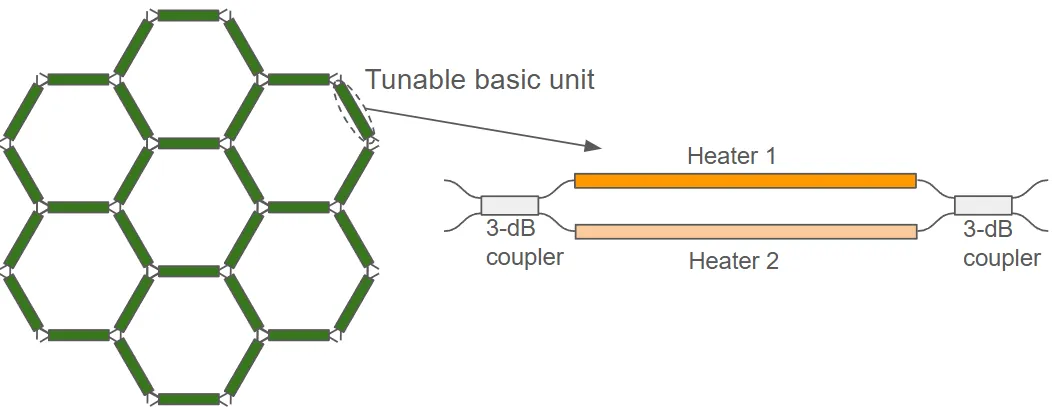
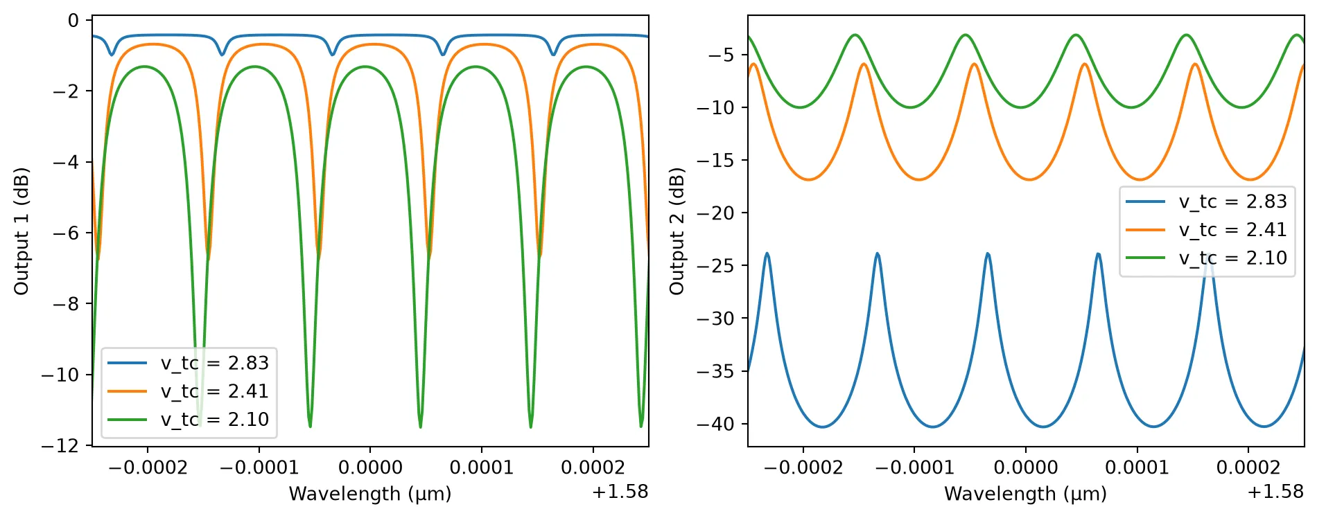
In this notebook, we create a programmable photonic circuit inspired by the works presented in [1] and [2]. This programmable circuit is based on a hexagonal lattice structure, where each link consists of a tunable Mach-Zehnder interferometer (MZI) with thermally controlled phase shifters on its arms. These thermal phase shifters allow us to individually adjust the optical path lengths, providing precise control over the interference within each MZI. By selectively tuning different units within the hexagonal lattice, we achieve a highly reconfigurable photonic platform capable of realizing various functional devices, such as unbalanced interferometers, finite impulse response (FIR) filters, add-drop filters, and more, as discussed in [1] and [2].
References
- Pérez, Daniel, et al. “Multipurpose silicon photonics signal processor core.” Nature communications 2017 8 (1), 636, doi: 10.1038/s41467-017-01529-w.
- Pérez-López, Daniel, et al. “Multipurpose self-configuration of programmable photonic circuits.” Nature communications 2020 11 (1), 6359. doi: 10.1038/s41467-020-19608-w.
- Guan, Hang, et al. “Compact and low loss 90° optical hybrid on a silicon-on-insulator platform.” Optics Express 2017 25 (23):,28957-28968. doi: 10.1364/OE.25.028957
import matplotlib.pyplot as pltimport numpy as npimport photonforge as pfimport siepic_forge as siepic_pdkimport tidy3d as tdfrom photonforge.live_viewer import LiveViewer
viewer = LiveViewer()
LiveViewer started at http://127.0.0.1:45149. Call its 'stop()' method to free the port.We start by defining several default parameters for the notebook, including loading the SiEPIC OpenEBL PDK which we will use throughout our design. We also specify the wavelength range of interest for our simulations, centered around 1.58 µm.
# Set the default port specification for TE polarizationport_spec = "TE_1550_500"
# Configure default parameters for photonic componentspf.config.default_kwargs = {    "port_spec": port_spec,  # specify the waveguide port type    "radius": 15,  # default bend radius    "euler_fraction": 0.5,  # Euler bend fraction}
# Load SiEPIC OpenEBL technology PDKtech = siepic_pdk.ebeam()
# Set the default technology to SiEPIC OpenEBLpf.config.default_technology = tech
# Define default mesh refinement levelpf.config.default_mesh_refinement = 12
# Set Tidy3D logging level to suppress non-critical messagestd.config.logging.level = "ERROR"
# Define wavelength range for the simulationwavelengths = np.linspace(1.5797, 1.5803, 401)
# Central wavelength at 1.58 µmlambda_0 = 1.58
# Convert wavelengths to frequenciesfrequencies = pf.C_0 / wavelengths
Tunable basic unit
Section titled “Tunable basic unit”Parametric 3-dB MMI Coupler
Section titled “Parametric 3-dB MMI Coupler”
We start by creating a 3-dB multimode interference (MMI) coupler inspired by [3]. Initially, we scale all dimensions according to our operating wavelength (1.58 µm) since the original design was for 1.55 µm (we also slightly increased l1 to get more even splitting). Then, to avoid port overlaps and reduce optical losses, we multiply all the widths by a factor of 1.35. Furthermore, according to the analytical expression for the beat length () of the MMI, given by:
the length is proportional to the square of the width. So, we scale all length dimensions by the square of this width-scaling factor (1.35²).
Below, we define the parametric component function for the 2x2 MMI coupler:
# Define a parametric 2x2 MMI splitter component@pf.parametric_componentdef mmi_2x2(    *,    l1=4.41,  # length of taper section at input    l2=4.51,  # length of intermediate taper section    l3=3.01,  # length of central multimode section    w1=2.05,  # intermediate width near input/output    w2=2.05,  # central section width    w5=0.972,  # input taper narrow width    w6=0.284,  # gap between input waveguides    port_spec=tech.ports["TE_1550_500"]  # port specification for waveguides):    """    Creates a parametric 2x2 multimode interference (MMI) splitter component.
    Parameters:        l1, l2, l3 (float): Section lengths.        w1, w2, w5, w6 (float): Section widths.        port_spec: Specification for the optical ports.
    Returns:        PhotonForge Component: Configured MMI with geometry and simulation model.    """    # Resolve port specification if provided as string    if isinstance(port_spec, str):        port_spec = pf.config.default_technology.ports[port_spec]
    # Initialize an empty component named "MMI2x2"    mmi = pf.Component("MMI2x2")
    # Extract default waveguide width from port specification    wg_width, _ = port_spec.path_profile_for("Si")
    # Calculate widths based on given parameters    w3 = 2 * w5 + w6    w4 = wg_width
    # Define paths for input and output waveguides    input_wg_up = pf.Path((0, (w5 + w6) / 2), w4).segment((l1, 0), w5, relative=True)    input_wg_down = input_wg_up.copy().mirror()    output_wg_up = input_wg_up.copy().mirror(        axis_endpoint=(l1 + l2 + l3, 1), axis_origin=(l1 + l2 + l3, 0)    )    output_wg_down = output_wg_up.copy().mirror()
    # Define the central multimode section of MMI    central_section = (        pf.Path((l1, 0), w3)        .segment((l2, 0), w1, relative=True)        .segment((l3, 0), w2, relative=True)        .segment((l3, 0), w2, relative=True)        .segment((l2, 0), w3, relative=True)    )
    # Add the defined geometries to the silicon ("Si") layer    mmi.add(        "Si", input_wg_up, input_wg_down, output_wg_up, output_wg_down, central_section    )
    # Automatically detect and add ports    mmi.add_port(mmi.detect_ports([port_spec]))    assert len(mmi.ports) == 4, "Port detection failed: expected exactly 4 ports."
    # Include the Tidy3D simulation model with specified port symmetries    mmi.add_model(        pf.Tidy3DModel(            port_symmetries=[                ("P1", "P0", "P3", "P2"),  # reflection symmetry about x axis                ("P2", "P3", "P0", "P1"),  # reflection symmetry about y axis                ("P3", "P2", "P1", "P0"),  # inversion symmetry about the origin            ],        ),        "Tidy3DModel",    )
    return mmi
# Instantiate the MMI component with default dimensionsmmi = mmi_2x2()
We now test and verify that the defined port symmetries of our MMI coupler are correct. This runs full simulations without assuming any symmetry, then compares the results against the model’s declared port_symmetries. It verifies if the symmetry settings are valid within a given tolerance (default atol=0.02).
# Define temporary wavelength range for symmetry testingwavelength_temp = np.linspace(1.5, 1.6, 11)
# Test the defined port symmetries (assert if test fails)assert mmi.active_model.test_port_symmetries(    mmi, frequencies=pf.C_0 / wavelength_temp, grid_spec=8)
Uploading task 'P0@0…'Uploading task 'P1@0…'Uploading task 'P2@0…'Uploading task 'P3@0…'Starting task 'P0@0': https://tidy3d.simulation.cloud/workbench?taskId=fdve-8d9e5c85-9c8b-4276-b3ae-2320bbf517cfStarting task 'P1@0': https://tidy3d.simulation.cloud/workbench?taskId=fdve-6fb571e8-1bb8-4eab-9d69-6224cc41fad5Downloading data from 'P0@0'…Starting task 'P2@0': https://tidy3d.simulation.cloud/workbench?taskId=fdve-9f703508-c9fa-464f-bd33-758bb5f5e75eStarting task 'P3@0': https://tidy3d.simulation.cloud/workbench?taskId=fdve-1a036231-0860-410c-b970-0bbf1efd5385Downloading data from 'P1@0'…Downloading data from 'P3@0'…Downloading data from 'P2@0'…We calculate the scattering matrix (S-matrix) for our MMI coupler at the defined wavelength range and visualize the results to evaluate its optical behavior. The total insertion loss is less than 0.08 dB and the power splits almost evenly between the output ports.
# Calculate the S-matrix of the MMI coupler over the specified wavelength ranges_matrix_mmi = mmi.s_matrix(pf.C_0 / wavelengths)
# Plot the calculated S-matrix_ = pf.plot_s_matrix(s_matrix_mmi)
Uploading task 'P0@0…'Starting task 'P0@0': https://tidy3d.simulation.cloud/workbench?taskId=fdve-b783ec9e-d3af-4d2e-8e60-f581d5ec96f0Downloading data from 'P0@0'…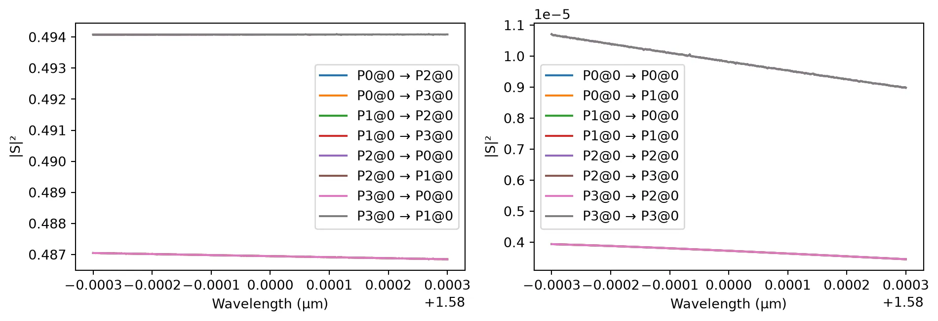
Wrapping the MMI with S-Bends for Input/Output Access
To improve routing and alignment within larger circuit designs, we encapsulate the 2×2 MMI with four S-bend waveguides. This setup ensures that the input and output ports are more spatially separated and accessible.
We instantiate the S-bends, connect them to the four ports of the MMI, and assign new external ports. The resulting composite component, named "MMI with S bends", is then visualized and assigned a circuit model for simulation (we avoid costly FDTD simulations because the S bends are very low loss).
# S-bend waveguide length and vertical displacementsbend_length = 20vertical_distance = 20
# Create a parametric S-bend waveguide with half vertical offsets_bend = pf.parametric.s_bend(length=sbend_length, offset=vertical_distance / 2)
# Create a new component to hold the MMI with attached S-bendsmmi_with_sbend = pf.Component("MMI with S bends")
# Add a reference to the original MMImmi_ref = mmi_with_sbend.add_reference(mmi)
# Add four references to S-bend for the four ports of the MMIs_bend0 = mmi_with_sbend.add_reference(s_bend)s_bend1 = mmi_with_sbend.add_reference(s_bend).mirror()  # mirror for port 1s_bend2 = mmi_with_sbend.add_reference(s_bend).mirror()  # mirror for port 2s_bend3 = mmi_with_sbend.add_reference(s_bend)
# Connect S-bends to the respective MMI portss_bend0.connect("P1", mmi_ref["P0"])s_bend1.connect("P1", mmi_ref["P1"])s_bend2.connect("P1", mmi_ref["P2"])s_bend3.connect("P1", mmi_ref["P3"])
# Add portsmmi_with_sbend.add_reference_ports()
# Add a simulation-ready circuit model to the componentmmi_with_sbend.add_model(pf.CircuitModel())
# Visualize the final MMI component with S-bend waveguidesviewer(mmi_with_sbend);fill:%23221f20;font-weight:bold;font-size:1.165680px;}.terminal{fill:none;stroke:%23805080;stroke-width:0.145710;}.dashed{stroke-dasharray:0.728550,0.437130;}.port{fill:none;stroke:%23805080;stroke-width:0.291420;}.virtual-connection{fill:none;stroke:%23907090;stroke-width:0.218565;}.layer_31_0{stroke:%238c78ef;fill:url(%23pat-layer_31_0);fill-opacity:0.492;}.label_31_0{fill:%238c78ef;}.layer_33_0{stroke:%238c78ef;fill:url(%23pat-layer_33_0);fill-opacity:0.492;}.label_33_0{fill:%238c78ef;}.layer_102_0{stroke:%238c78ef;fill:url(%23pat-layer_102_0);fill-opacity:0.492;}.label_102_0{fill:%238c78ef;}.layer_110_0{stroke:%238c78ef;fill:url(%23pat-layer_110_0);fill-opacity:0.492;}.label_110_0{fill:%238c78ef;}.layer_189_0{stroke:%23000000;fill:none;}.label_189_0{fill:%23000000;}.layer_201_0{stroke:%2300ee00;fill:url(%23pat-layer_201_0);fill-opacity:0.492;}.label_201_0{fill:%2300ee00;}.layer_401_0{stroke:%236a8ad2;fill:url(%23pat-layer_401_0);fill-opacity:0.492;}.label_401_0{fill:%236a8ad2;}.layer_202_0{stroke:%23007600;fill:url(%23pat-layer_202_0);fill-opacity:0.492;}.label_202_0{fill:%23007600;}.layer_68_0{stroke:%23008000;fill:url(%23pat-layer_68_0);fill-opacity:0.492;}.label_68_0{fill:%23008000;}.layer_5_0{stroke:%236a8ad2;fill:url(%23pat-layer_5_0);fill-opacity:0.492;}.label_5_0{fill:%236a8ad2;}.layer_998_0{stroke:%23000000;fill:none;}.label_998_0{fill:%23000000;}.layer_312_1{stroke:%2300b8b8;fill:url(%23pat-layer_312_1);fill-opacity:0.492;}.label_312_1{fill:%2300b8b8;}.layer_312_0{stroke:%2300b8b8;fill:url(%23pat-layer_312_0);fill-opacity:0.492;}.label_312_0{fill:%2300b8b8;}.layer_402_0{stroke:%23ff0000;fill:url(%23pat-layer_402_0);fill-opacity:0.492;}.label_402_0{fill:%23ff0000;}.layer_401_4{stroke:%236a8ad2;fill:url(%23pat-layer_401_4);fill-opacity:0.492;}.label_401_4{fill:%236a8ad2;}.layer_389_0{stroke:%23ff00ff;fill:url(%23pat-layer_389_0);fill-opacity:0.492;}.label_389_0{fill:%23ff00ff;}.layer_402_1{stroke:%23ff0000;fill:url(%23pat-layer_402_1);fill-opacity:0.492;}.label_402_1{fill:%23ff0000;}.layer_350_1{stroke:%23697a00;fill:url(%23pat-layer_350_1);fill-opacity:0.492;}.label_350_1{fill:%23697a00;}.layer_401_1{stroke:%236a8ad2;fill:url(%23pat-layer_401_1);fill-opacity:0.492;}.label_401_1{fill:%236a8ad2;}.layer_313_2{stroke:%2301d95b;fill:url(%23pat-layer_313_2);fill-opacity:0.492;}.label_313_2{fill:%2301d95b;}.layer_313_1{stroke:%2301d95b;fill:url(%23pat-layer_313_1);fill-opacity:0.492;}.label_313_1{fill:%2301d95b;}.layer_313_0{stroke:%2301d95b;fill:url(%23pat-layer_313_0);fill-opacity:0.492;}.label_313_0{fill:%2301d95b;}.layer_400_0{stroke:%23a96868;fill:url(%23pat-layer_400_0);fill-opacity:0.492;}.label_400_0{fill:%23a96868;}.layer_312_3{stroke:%2300b8b8;fill:url(%23pat-layer_312_3);fill-opacity:0.492;}.label_312_3{fill:%2300b8b8;}.layer_389_1{stroke:%23ff00ff;fill:url(%23pat-layer_389_1);fill-opacity:0.492;}.label_389_1{fill:%23ff00ff;}.layer_401_3{stroke:%236a8ad2;fill:url(%23pat-layer_401_3);fill-opacity:0.492;}.label_401_3{fill:%236a8ad2;}.layer_403_2{stroke:%23500080;fill:url(%23pat-layer_403_2);fill-opacity:0.492;}.label_403_2{fill:%23500080;}.layer_403_3{stroke:%23500080;fill:url(%23pat-layer_403_3);fill-opacity:0.492;}.label_403_3{fill:%23500080;}.layer_403_1{stroke:%23500080;fill:url(%23pat-layer_403_1);fill-opacity:0.492;}.label_403_1{fill:%23500080;}.layer_403_0{stroke:%23500080;fill:url(%23pat-layer_403_0);fill-opacity:0.492;}.label_403_0{fill:%23500080;}.layer_311_1{stroke:%23ac6c56;fill:url(%23pat-layer_311_1);fill-opacity:0.492;}.label_311_1{fill:%23ac6c56;}.layer_311_0{stroke:%23ac6c56;fill:url(%23pat-layer_311_0);fill-opacity:0.492;}.label_311_0{fill:%23ac6c56;}.layer_301_1{stroke:%23800057;fill:url(%23pat-layer_301_1);fill-opacity:0.492;}.label_301_1{fill:%23800057;}.layer_301_0{stroke:%23800057;fill:url(%23pat-layer_301_0);fill-opacity:0.492;}.label_301_0{fill:%23800057;}.layer_305_1{stroke:%23808080;fill:url(%23pat-layer_305_1);fill-opacity:0.492;}.label_305_1{fill:%23808080;}.layer_305_0{stroke:%23808080;fill:url(%23pat-layer_305_0);fill-opacity:0.492;}.label_305_0{fill:%23808080;}.layer_999_0{stroke:%230000ff;fill:url(%23pat-layer_999_0);fill-opacity:0.492;}.label_999_0{fill:%230000ff;}.layer_81_0{stroke:%23808080;fill:url(%23pat-layer_81_0);fill-opacity:0.492;}.label_81_0{fill:%23808080;}.layer_290_0{stroke:%23a46eda;fill:none;}.label_290_0{fill:%23a46eda;}.layer_205_0{stroke:%2349b203;fill:url(%23pat-layer_205_0);fill-opacity:0.492;}.label_205_0{fill:%2349b203;}.layer_11_0{stroke:%230000ff;fill:url(%23pat-layer_11_0);fill-opacity:0.492;}.label_11_0{fill:%230000ff;}.layer_12_0{stroke:%23a57b00;fill:url(%23pat-layer_12_0);fill-opacity:0.492;}.label_12_0{fill:%23a57b00;}.layer_13_0{stroke:%23800057;fill:url(%23pat-layer_13_0);fill-opacity:0.492;}.label_13_0{fill:%23800057;}.layer_6_0{stroke:%23ff0000;fill:url(%23pat-layer_6_0);fill-opacity:0.492;}.label_6_0{fill:%23ff0000;}.layer_1_10{stroke:%23c96585;fill:url(%23pat-layer_1_10);fill-opacity:0.492;}.label_1_10{fill:%23c96585;}.layer_1_11{stroke:%23800000;fill:url(%23pat-layer_1_11);fill-opacity:0.492;}.label_1_11{fill:%23800000;}.layer_200_0{stroke:%23ff0000;fill:url(%23pat-layer_200_0);fill-opacity:0.492;}.label_200_0{fill:%23ff0000;}.layer_1_0{stroke:%23c96585;fill:url(%23pat-layer_1_0);fill-opacity:0.492;}.label_1_0{fill:%23c96585;}.layer_2_0{stroke:%23a46eda;fill:url(%23pat-layer_2_0);fill-opacity:0.492;}.label_2_0{fill:%23a46eda;}.layer_20_0{stroke:%2353793d;fill:url(%23pat-layer_20_0);fill-opacity:0.492;}.label_20_0{fill:%2353793d;}.layer_22_0{stroke:%23ec7600;fill:url(%23pat-layer_22_0);fill-opacity:0.492;}.label_22_0{fill:%23ec7600;}.layer_24_0{stroke:%2300b8b8;fill:url(%23pat-layer_24_0);fill-opacity:0.492;}.label_24_0{fill:%2300b8b8;}.layer_21_0{stroke:%23736264;fill:url(%23pat-layer_21_0);fill-opacity:0.492;}.label_21_0{fill:%23736264;}.layer_23_0{stroke:%23697a00;fill:url(%23pat-layer_23_0);fill-opacity:0.492;}.label_23_0{fill:%23697a00;}.layer_25_0{stroke:%23008000;fill:url(%23pat-layer_25_0);fill-opacity:0.492;}.label_25_0{fill:%23008000;}.layer_350_0{stroke:%23697a00;fill:url(%23pat-layer_350_0);fill-opacity:0.492;}.label_350_0{fill:%23697a00;}.layer_10_0{stroke:%23000000;fill:none;}.label_10_0{fill:%23000000;}.layer_203_0{stroke:%23008000;fill:url(%23pat-layer_203_0);fill-opacity:0.492;}.label_203_0{fill:%23008000;}.layer_40_0{stroke:%230000ff;fill:url(%23pat-layer_40_0);fill-opacity:0.492;}.label_40_0{fill:%230000ff;}.layer_401_2{stroke:%236a8ad2;fill:url(%23pat-layer_401_2);fill-opacity:0.492;}.label_401_2{fill:%236a8ad2;}.layer_301_2{stroke:%23800057;fill:url(%23pat-layer_301_2);fill-opacity:0.492;}.label_301_2{fill:%23800057;}</style><defs><path id=%22port-symbol%22 class=%22port%22 d=%22M 0,-0.582840 L 0.874260,0 0,0.582840%22 /><path id=%22ref-port-symbol%22 class=%22port%22 style=%22stroke-opacity:0.33;%22 d=%22M 0,-0.437130 C 0.582840,-0.437130 0.582840,0.437130 0,0.437130%22 /><circle id=%22port-bend-symbol%22 style=%22stroke-width:0;stroke:none;fill:%23805080;fill-opacity:1;%22 cx=%220%22 cy=%220%22 r=%220.262278%22 /><circle id=%22connection-symbol%22 style=%22stroke-width:0;stroke:none;fill:%23907090;fill-opacity:1;%22 cx=%220%22 cy=%220%22 r=%220.305991%22 /><pattern id=%22pat-layer_31_0%22 patternUnits=%22userSpaceOnUse%22 width=%220.728550%22 height=%220.728550%22 patternTransform=%22translate(0.557126,0.690205)%22><line x1=%220%22 y1=%220%22 x2=%220.728550%22 y2=%220.728550%22 style=%22stroke:%238c78ef;stroke-width:0.072855%22 /><line x1=%22-0.364275%22 y1=%220.364275%22 x2=%220.364275%22 y2=%221.092825%22 style=%22stroke:%238c78ef;stroke-width:0.072855%22 /><line x1=%220.364275%22 y1=%22-0.364275%22 x2=%221.092825%22 y2=%220.364275%22 style=%22stroke:%238c78ef;stroke-width:0.072855%22 /></pattern><pattern id=%22pat-layer_33_0%22 patternUnits=%22userSpaceOnUse%22 width=%220.728550%22 height=%220.728550%22 patternTransform=%22translate(0.428559,0.076689)%22><line x1=%220%22 y1=%220%22 x2=%220.728550%22 y2=%220.728550%22 style=%22stroke:%238c78ef;stroke-width:0.072855%22 /><line x1=%22-0.364275%22 y1=%220.364275%22 x2=%220.364275%22 y2=%221.092825%22 style=%22stroke:%238c78ef;stroke-width:0.072855%22 /><line x1=%220.364275%22 y1=%22-0.364275%22 x2=%221.092825%22 y2=%220.364275%22 style=%22stroke:%238c78ef;stroke-width:0.072855%22 /></pattern><pattern id=%22pat-layer_102_0%22 patternUnits=%22userSpaceOnUse%22 width=%220.728550%22 height=%220.728550%22 patternTransform=%22translate(0.000000,0.038345)%22><line x1=%220%22 y1=%220%22 x2=%220.728550%22 y2=%220.728550%22 style=%22stroke:%238c78ef;stroke-width:0.072855%22 /><line x1=%22-0.364275%22 y1=%220.364275%22 x2=%220.364275%22 y2=%221.092825%22 style=%22stroke:%238c78ef;stroke-width:0.072855%22 /><line x1=%220.364275%22 y1=%22-0.364275%22 x2=%221.092825%22 y2=%220.364275%22 style=%22stroke:%238c78ef;stroke-width:0.072855%22 /></pattern><pattern id=%22pat-layer_110_0%22 patternUnits=%22userSpaceOnUse%22 width=%220.728550%22 height=%220.728550%22 patternTransform=%22translate(0.214279,0.498482)%22><line x1=%220%22 y1=%220%22 x2=%220.728550%22 y2=%220.728550%22 style=%22stroke:%238c78ef;stroke-width:0.072855%22 /><line x1=%22-0.364275%22 y1=%220.364275%22 x2=%220.364275%22 y2=%221.092825%22 style=%22stroke:%238c78ef;stroke-width:0.072855%22 /><line x1=%220.364275%22 y1=%22-0.364275%22 x2=%221.092825%22 y2=%220.364275%22 style=%22stroke:%238c78ef;stroke-width:0.072855%22 /></pattern><pattern id=%22pat-layer_201_0%22 patternUnits=%22userSpaceOnUse%22 width=%220.728550%22 height=%220.728550%22 patternTransform=%22translate(0.557126,0.268413)%22><circle cx=%220.364275%22 cy=%220.364275%22 r=%220.072855%22 style=%22stroke:none;fill:%2300ee00;fill-opacity:1.0%22 /></pattern><pattern id=%22pat-layer_401_0%22 patternUnits=%22userSpaceOnUse%22 width=%220.437130%22 height=%220.437130%22 patternTransform=%22translate(0.051427,0.069021)%22><line x1=%220%22 y1=%220%22 x2=%220.437130%22 y2=%220.437130%22 style=%22stroke:%236a8ad2;stroke-width:0.072855%22 /><line x1=%22-0.218565%22 y1=%220.218565%22 x2=%220.218565%22 y2=%220.655695%22 style=%22stroke:%236a8ad2;stroke-width:0.072855%22 /><line x1=%220.218565%22 y1=%22-0.218565%22 x2=%220.655695%22 y2=%220.218565%22 style=%22stroke:%236a8ad2;stroke-width:0.072855%22 /><line x1=%220.437130%22 y1=%220%22 x2=%220%22 y2=%220.437130%22 style=%22stroke:%236a8ad2;stroke-width:0.072855%22 /><line x1=%220.655695%22 y1=%220.218565%22 x2=%220.218565%22 y2=%220.655695%22 style=%22stroke:%236a8ad2;stroke-width:0.072855%22 /><line x1=%220.218565%22 y1=%22-0.218565%22 x2=%22-0.218565%22 y2=%220.218565%22 style=%22stroke:%236a8ad2;stroke-width:0.072855%22 /></pattern><pattern id=%22pat-layer_202_0%22 patternUnits=%22userSpaceOnUse%22 width=%220.437130%22 height=%220.437130%22 patternTransform=%22translate(0.077141,0.414123)%22><circle cx=%220.218565%22 cy=%220.218565%22 r=%220.072855%22 style=%22stroke:none;fill:%23007600;fill-opacity:1.0%22 /></pattern><pattern id=%22pat-layer_68_0%22 patternUnits=%22userSpaceOnUse%22 width=%220.728550%22 height=%220.728550%22 patternTransform=%22translate(0.000000,0.268413)%22><circle cx=%220.364275%22 cy=%220.364275%22 r=%220.072855%22 style=%22stroke:none;fill:%23008000;fill-opacity:1.0%22 /></pattern><pattern id=%22pat-layer_5_0%22 patternUnits=%22userSpaceOnUse%22 width=%220.437130%22 height=%220.437130%22 patternTransform=%22translate(0.025714,0.391116)%22><line x1=%220.218565%22 y1=%220%22 x2=%220.218565%22 y2=%220.437130%22 style=%22stroke:%236a8ad2;stroke-width:0.072855%22 /></pattern><pattern id=%22pat-layer_312_1%22 patternUnits=%22userSpaceOnUse%22 width=%220.437130%22 height=%220.437130%22 patternTransform=%22translate(0.102854,0.345103)%22><line x1=%220%22 y1=%220%22 x2=%220.437130%22 y2=%220.437130%22 style=%22stroke:%2300b8b8;stroke-width:0.072855%22 /><line x1=%22-0.218565%22 y1=%220.218565%22 x2=%220.218565%22 y2=%220.655695%22 style=%22stroke:%2300b8b8;stroke-width:0.072855%22 /><line x1=%220.218565%22 y1=%22-0.218565%22 x2=%220.655695%22 y2=%220.218565%22 style=%22stroke:%2300b8b8;stroke-width:0.072855%22 /></pattern><pattern id=%22pat-layer_312_0%22 patternUnits=%22userSpaceOnUse%22 width=%220.728550%22 height=%220.728550%22 patternTransform=%22translate(0.342847,0.460137)%22><line x1=%220.364275%22 y1=%220%22 x2=%220.364275%22 y2=%220.728550%22 style=%22stroke:%2300b8b8;stroke-width:0.072855%22 /></pattern><pattern id=%22pat-layer_402_0%22 patternUnits=%22userSpaceOnUse%22 width=%220.728550%22 height=%220.728550%22 patternTransform=%22translate(0.385703,0.536826)%22><line x1=%220.364275%22 y1=%220%22 x2=%220.364275%22 y2=%220.728550%22 style=%22stroke:%23ff0000;stroke-width:0.072855%22 /><line x1=%220%22 y1=%220.364275%22 x2=%220.728550%22 y2=%220.364275%22 style=%22stroke:%23ff0000;stroke-width:0.072855%22 /></pattern><pattern id=%22pat-layer_401_4%22 patternUnits=%22userSpaceOnUse%22 width=%220.437130%22 height=%220.437130%22 patternTransform=%22translate(0.077141,0.345103)%22><line x1=%220.218565%22 y1=%220%22 x2=%220.218565%22 y2=%220.437130%22 style=%22stroke:%236a8ad2;stroke-width:0.072855%22 /></pattern><pattern id=%22pat-layer_389_0%22 patternUnits=%22userSpaceOnUse%22 width=%220.437130%22 height=%220.437130%22 patternTransform=%22translate(0.077141,0.092027)%22><line x1=%220.218565%22 y1=%220%22 x2=%220.218565%22 y2=%220.437130%22 style=%22stroke:%23ff00ff;stroke-width:0.072855%22 /><line x1=%220%22 y1=%220.218565%22 x2=%220.437130%22 y2=%220.218565%22 style=%22stroke:%23ff00ff;stroke-width:0.072855%22 /></pattern><pattern id=%22pat-layer_402_1%22 patternUnits=%22userSpaceOnUse%22 width=%220.437130%22 height=%220.437130%22 patternTransform=%22translate(0.128568,0.391116)%22><line x1=%220%22 y1=%220%22 x2=%220.437130%22 y2=%220.437130%22 style=%22stroke:%23ff0000;stroke-width:0.072855%22 /><line x1=%22-0.218565%22 y1=%220.218565%22 x2=%220.218565%22 y2=%220.655695%22 style=%22stroke:%23ff0000;stroke-width:0.072855%22 /><line x1=%220.218565%22 y1=%22-0.218565%22 x2=%220.655695%22 y2=%220.218565%22 style=%22stroke:%23ff0000;stroke-width:0.072855%22 /><line x1=%220.437130%22 y1=%220%22 x2=%220%22 y2=%220.437130%22 style=%22stroke:%23ff0000;stroke-width:0.072855%22 /><line x1=%220.655695%22 y1=%220.218565%22 x2=%220.218565%22 y2=%220.655695%22 style=%22stroke:%23ff0000;stroke-width:0.072855%22 /><line x1=%220.218565%22 y1=%22-0.218565%22 x2=%22-0.218565%22 y2=%220.218565%22 style=%22stroke:%23ff0000;stroke-width:0.072855%22 /></pattern><pattern id=%22pat-layer_350_1%22 patternUnits=%22userSpaceOnUse%22 width=%220.437130%22 height=%220.437130%22 patternTransform=%22translate(0.385703,0.345103)%22><circle cx=%220.218565%22 cy=%220.218565%22 r=%220.072855%22 style=%22stroke:none;fill:%23697a00;fill-opacity:1.0%22 /></pattern><pattern id=%22pat-layer_401_1%22 patternUnits=%22userSpaceOnUse%22 width=%220.728550%22 height=%220.728550%22 patternTransform=%22translate(0.642838,0.230068)%22><line x1=%220%22 y1=%220%22 x2=%220.728550%22 y2=%220.728550%22 style=%22stroke:%236a8ad2;stroke-width:0.072855%22 /><line x1=%22-0.364275%22 y1=%220.364275%22 x2=%220.364275%22 y2=%221.092825%22 style=%22stroke:%236a8ad2;stroke-width:0.072855%22 /><line x1=%220.364275%22 y1=%22-0.364275%22 x2=%221.092825%22 y2=%220.364275%22 style=%22stroke:%236a8ad2;stroke-width:0.072855%22 /><line x1=%220.728550%22 y1=%220%22 x2=%220%22 y2=%220.728550%22 style=%22stroke:%236a8ad2;stroke-width:0.072855%22 /><line x1=%221.092825%22 y1=%220.364275%22 x2=%220.364275%22 y2=%221.092825%22 style=%22stroke:%236a8ad2;stroke-width:0.072855%22 /><line x1=%220.364275%22 y1=%22-0.364275%22 x2=%22-0.364275%22 y2=%220.364275%22 style=%22stroke:%236a8ad2;stroke-width:0.072855%22 /></pattern><pattern id=%22pat-layer_313_2%22 patternUnits=%22userSpaceOnUse%22 width=%220.437130%22 height=%220.437130%22 patternTransform=%22translate(0.179995,0.230068)%22><line x1=%220%22 y1=%220%22 x2=%220.437130%22 y2=%220.437130%22 style=%22stroke:%2301d95b;stroke-width:0.072855%22 /><line x1=%22-0.218565%22 y1=%220.218565%22 x2=%220.218565%22 y2=%220.655695%22 style=%22stroke:%2301d95b;stroke-width:0.072855%22 /><line x1=%220.218565%22 y1=%22-0.218565%22 x2=%220.655695%22 y2=%220.218565%22 style=%22stroke:%2301d95b;stroke-width:0.072855%22 /></pattern><pattern id=%22pat-layer_313_1%22 patternUnits=%22userSpaceOnUse%22 width=%220.728550%22 height=%220.728550%22 patternTransform=%22translate(0.471415,0.268413)%22><line x1=%220.364275%22 y1=%220%22 x2=%220.364275%22 y2=%220.728550%22 style=%22stroke:%2301d95b;stroke-width:0.072855%22 /></pattern><pattern id=%22pat-layer_313_0%22 patternUnits=%22userSpaceOnUse%22 width=%220.437130%22 height=%220.437130%22 patternTransform=%22translate(0.385703,0.092027)%22><line x1=%220.218565%22 y1=%220%22 x2=%220.218565%22 y2=%220.437130%22 style=%22stroke:%2301d95b;stroke-width:0.072855%22 /></pattern><pattern id=%22pat-layer_400_0%22 patternUnits=%22userSpaceOnUse%22 width=%220.728550%22 height=%220.728550%22 patternTransform=%22translate(0.514271,0.421792)%22><line x1=%220%22 y1=%220%22 x2=%220.728550%22 y2=%220.728550%22 style=%22stroke:%23a96868;stroke-width:0.072855%22 /><line x1=%22-0.364275%22 y1=%220.364275%22 x2=%220.364275%22 y2=%221.092825%22 style=%22stroke:%23a96868;stroke-width:0.072855%22 /><line x1=%220.364275%22 y1=%22-0.364275%22 x2=%221.092825%22 y2=%220.364275%22 style=%22stroke:%23a96868;stroke-width:0.072855%22 /><line x1=%220.728550%22 y1=%220%22 x2=%220%22 y2=%220.728550%22 style=%22stroke:%23a96868;stroke-width:0.072855%22 /><line x1=%221.092825%22 y1=%220.364275%22 x2=%220.364275%22 y2=%221.092825%22 style=%22stroke:%23a96868;stroke-width:0.072855%22 /><line x1=%220.364275%22 y1=%22-0.364275%22 x2=%22-0.364275%22 y2=%220.364275%22 style=%22stroke:%23a96868;stroke-width:0.072855%22 /></pattern><pattern id=%22pat-layer_312_3%22 patternUnits=%22userSpaceOnUse%22 width=%220.437130%22 height=%220.437130%22 patternTransform=%22translate(0.334276,0.046014)%22><line x1=%220.437130%22 y1=%220%22 x2=%220%22 y2=%220.437130%22 style=%22stroke:%2300b8b8;stroke-width:0.072855%22 /><line x1=%220.655695%22 y1=%220.218565%22 x2=%220.218565%22 y2=%220.655695%22 style=%22stroke:%2300b8b8;stroke-width:0.072855%22 /><line x1=%220.218565%22 y1=%22-0.218565%22 x2=%22-0.218565%22 y2=%220.218565%22 style=%22stroke:%2300b8b8;stroke-width:0.072855%22 /></pattern><pattern id=%22pat-layer_389_1%22 patternUnits=%22userSpaceOnUse%22 width=%220.728550%22 height=%220.728550%22 patternTransform=%22translate(0.685694,0.268413)%22><line x1=%220.364275%22 y1=%220%22 x2=%220.364275%22 y2=%220.728550%22 style=%22stroke:%23ff00ff;stroke-width:0.072855%22 /><line x1=%220%22 y1=%220.364275%22 x2=%220.728550%22 y2=%220.364275%22 style=%22stroke:%23ff00ff;stroke-width:0.072855%22 /></pattern><pattern id=%22pat-layer_401_3%22 patternUnits=%22userSpaceOnUse%22 width=%220.728550%22 height=%220.728550%22 patternTransform=%22translate(0.299991,0.460137)%22><line x1=%220%22 y1=%220.364275%22 x2=%220.728550%22 y2=%220.364275%22 style=%22stroke:%236a8ad2;stroke-width:0.072855%22 /></pattern><pattern id=%22pat-layer_403_2%22 patternUnits=%22userSpaceOnUse%22 width=%220.437130%22 height=%220.437130%22 patternTransform=%22translate(0.205708,0.276082)%22><line x1=%220%22 y1=%220%22 x2=%220.437130%22 y2=%220.437130%22 style=%22stroke:%23500080;stroke-width:0.072855%22 /><line x1=%22-0.218565%22 y1=%220.218565%22 x2=%220.218565%22 y2=%220.655695%22 style=%22stroke:%23500080;stroke-width:0.072855%22 /><line x1=%220.218565%22 y1=%22-0.218565%22 x2=%220.655695%22 y2=%220.218565%22 style=%22stroke:%23500080;stroke-width:0.072855%22 /><line x1=%220.437130%22 y1=%220%22 x2=%220%22 y2=%220.437130%22 style=%22stroke:%23500080;stroke-width:0.072855%22 /><line x1=%220.655695%22 y1=%220.218565%22 x2=%220.218565%22 y2=%220.655695%22 style=%22stroke:%23500080;stroke-width:0.072855%22 /><line x1=%220.218565%22 y1=%22-0.218565%22 x2=%22-0.218565%22 y2=%220.218565%22 style=%22stroke:%23500080;stroke-width:0.072855%22 /></pattern><pattern id=%22pat-layer_403_3%22 patternUnits=%22userSpaceOnUse%22 width=%220.728550%22 height=%220.728550%22 patternTransform=%22translate(0.171424,0.575171)%22><line x1=%220%22 y1=%220%22 x2=%220.728550%22 y2=%220.728550%22 style=%22stroke:%23500080;stroke-width:0.072855%22 /><line x1=%22-0.364275%22 y1=%220.364275%22 x2=%220.364275%22 y2=%221.092825%22 style=%22stroke:%23500080;stroke-width:0.072855%22 /><line x1=%220.364275%22 y1=%22-0.364275%22 x2=%221.092825%22 y2=%220.364275%22 style=%22stroke:%23500080;stroke-width:0.072855%22 /><line x1=%220.728550%22 y1=%220%22 x2=%220%22 y2=%220.728550%22 style=%22stroke:%23500080;stroke-width:0.072855%22 /><line x1=%221.092825%22 y1=%220.364275%22 x2=%220.364275%22 y2=%221.092825%22 style=%22stroke:%23500080;stroke-width:0.072855%22 /><line x1=%220.364275%22 y1=%22-0.364275%22 x2=%22-0.364275%22 y2=%220.364275%22 style=%22stroke:%23500080;stroke-width:0.072855%22 /></pattern><pattern id=%22pat-layer_403_1%22 patternUnits=%22userSpaceOnUse%22 width=%220.728550%22 height=%220.728550%22 patternTransform=%22translate(0.514271,0.345103)%22><line x1=%220.364275%22 y1=%220%22 x2=%220.364275%22 y2=%220.728550%22 style=%22stroke:%23500080;stroke-width:0.072855%22 /><line x1=%220%22 y1=%220.364275%22 x2=%220.728550%22 y2=%220.364275%22 style=%22stroke:%23500080;stroke-width:0.072855%22 /></pattern><pattern id=%22pat-layer_403_0%22 patternUnits=%22userSpaceOnUse%22 width=%220.437130%22 height=%220.437130%22 patternTransform=%22translate(0.411416,0.138041)%22><line x1=%220.218565%22 y1=%220%22 x2=%220.218565%22 y2=%220.437130%22 style=%22stroke:%23500080;stroke-width:0.072855%22 /><line x1=%220%22 y1=%220.218565%22 x2=%220.437130%22 y2=%220.218565%22 style=%22stroke:%23500080;stroke-width:0.072855%22 /></pattern><pattern id=%22pat-layer_311_1%22 patternUnits=%22userSpaceOnUse%22 width=%220.728550%22 height=%220.728550%22 patternTransform=%22translate(0.599982,0.153379)%22><line x1=%220%22 y1=%220%22 x2=%220.728550%22 y2=%220.728550%22 style=%22stroke:%23ac6c56;stroke-width:0.072855%22 /><line x1=%22-0.364275%22 y1=%220.364275%22 x2=%220.364275%22 y2=%221.092825%22 style=%22stroke:%23ac6c56;stroke-width:0.072855%22 /><line x1=%220.364275%22 y1=%22-0.364275%22 x2=%221.092825%22 y2=%220.364275%22 style=%22stroke:%23ac6c56;stroke-width:0.072855%22 /></pattern><pattern id=%22pat-layer_311_0%22 patternUnits=%22userSpaceOnUse%22 width=%220.437130%22 height=%220.437130%22 patternTransform=%22translate(0.025714,0.023007)%22><line x1=%220%22 y1=%220%22 x2=%220.437130%22 y2=%220.437130%22 style=%22stroke:%23ac6c56;stroke-width:0.072855%22 /><line x1=%22-0.218565%22 y1=%220.218565%22 x2=%220.218565%22 y2=%220.655695%22 style=%22stroke:%23ac6c56;stroke-width:0.072855%22 /><line x1=%220.218565%22 y1=%22-0.218565%22 x2=%220.655695%22 y2=%220.218565%22 style=%22stroke:%23ac6c56;stroke-width:0.072855%22 /></pattern><pattern id=%22pat-layer_301_1%22 patternUnits=%22userSpaceOnUse%22 width=%220.728550%22 height=%220.728550%22 patternTransform=%22translate(0.514271,0.306758)%22><line x1=%220%22 y1=%220.364275%22 x2=%220.728550%22 y2=%220.364275%22 style=%22stroke:%23800057;stroke-width:0.072855%22 /></pattern><pattern id=%22pat-layer_301_0%22 patternUnits=%22userSpaceOnUse%22 width=%220.437130%22 height=%220.437130%22 patternTransform=%22translate(0.411416,0.115034)%22><line x1=%220%22 y1=%220.218565%22 x2=%220.437130%22 y2=%220.218565%22 style=%22stroke:%23800057;stroke-width:0.072855%22 /></pattern><pattern id=%22pat-layer_305_1%22 patternUnits=%22userSpaceOnUse%22 width=%220.728550%22 height=%220.728550%22 patternTransform=%22translate(0.257135,0.536826)%22><line x1=%220.364275%22 y1=%220%22 x2=%220.364275%22 y2=%220.728550%22 style=%22stroke:%23808080;stroke-width:0.072855%22 /><line x1=%220%22 y1=%220.364275%22 x2=%220.728550%22 y2=%220.364275%22 style=%22stroke:%23808080;stroke-width:0.072855%22 /></pattern><pattern id=%22pat-layer_305_0%22 patternUnits=%22userSpaceOnUse%22 width=%220.437130%22 height=%220.437130%22 patternTransform=%22translate(0.257135,0.253075)%22><line x1=%220.218565%22 y1=%220%22 x2=%220.218565%22 y2=%220.437130%22 style=%22stroke:%23808080;stroke-width:0.072855%22 /><line x1=%220%22 y1=%220.218565%22 x2=%220.437130%22 y2=%220.218565%22 style=%22stroke:%23808080;stroke-width:0.072855%22 /></pattern><pattern id=%22pat-layer_999_0%22 patternUnits=%22userSpaceOnUse%22 width=%220.437130%22 height=%220.437130%22 patternTransform=%22translate(0.154281,0.161048)%22><line x1=%220.218565%22 y1=%220%22 x2=%220.218565%22 y2=%220.437130%22 style=%22stroke:%230000ff;stroke-width:0.072855%22 /></pattern><pattern id=%22pat-layer_81_0%22 patternUnits=%22userSpaceOnUse%22 width=%220.437130%22 height=%220.437130%22 patternTransform=%22translate(0.154281,0.391116)%22><line x1=%220.218565%22 y1=%220%22 x2=%220.218565%22 y2=%220.437130%22 style=%22stroke:%23808080;stroke-width:0.072855%22 /><line x1=%220%22 y1=%220.218565%22 x2=%220.437130%22 y2=%220.218565%22 style=%22stroke:%23808080;stroke-width:0.072855%22 /></pattern><pattern id=%22pat-layer_205_0%22 patternUnits=%22userSpaceOnUse%22 width=%220.437130%22 height=%220.437130%22 patternTransform=%22translate(0.179995,0.299089)%22><line x1=%220%22 y1=%220%22 x2=%220.437130%22 y2=%220.437130%22 style=%22stroke:%2349b203;stroke-width:0.072855%22 /><line x1=%22-0.218565%22 y1=%220.218565%22 x2=%220.218565%22 y2=%220.655695%22 style=%22stroke:%2349b203;stroke-width:0.072855%22 /><line x1=%220.218565%22 y1=%22-0.218565%22 x2=%220.655695%22 y2=%220.218565%22 style=%22stroke:%2349b203;stroke-width:0.072855%22 /><line x1=%220.437130%22 y1=%220%22 x2=%220%22 y2=%220.437130%22 style=%22stroke:%2349b203;stroke-width:0.072855%22 /><line x1=%220.655695%22 y1=%220.218565%22 x2=%220.218565%22 y2=%220.655695%22 style=%22stroke:%2349b203;stroke-width:0.072855%22 /><line x1=%220.218565%22 y1=%22-0.218565%22 x2=%22-0.218565%22 y2=%220.218565%22 style=%22stroke:%2349b203;stroke-width:0.072855%22 /></pattern><pattern id=%22pat-layer_11_0%22 patternUnits=%22userSpaceOnUse%22 width=%220.437130%22 height=%220.437130%22 patternTransform=%22translate(0.231422,0.161048)%22><line x1=%220.437130%22 y1=%220%22 x2=%220%22 y2=%220.437130%22 style=%22stroke:%230000ff;stroke-width:0.072855%22 /><line x1=%220.655695%22 y1=%220.218565%22 x2=%220.218565%22 y2=%220.655695%22 style=%22stroke:%230000ff;stroke-width:0.072855%22 /><line x1=%220.218565%22 y1=%22-0.218565%22 x2=%22-0.218565%22 y2=%220.218565%22 style=%22stroke:%230000ff;stroke-width:0.072855%22 /></pattern><pattern id=%22pat-layer_12_0%22 patternUnits=%22userSpaceOnUse%22 width=%220.437130%22 height=%220.437130%22 patternTransform=%22translate(0.411416,0.414123)%22><line x1=%220%22 y1=%220%22 x2=%220.437130%22 y2=%220.437130%22 style=%22stroke:%23a57b00;stroke-width:0.072855%22 /><line x1=%22-0.218565%22 y1=%220.218565%22 x2=%220.218565%22 y2=%220.655695%22 style=%22stroke:%23a57b00;stroke-width:0.072855%22 /><line x1=%220.218565%22 y1=%22-0.218565%22 x2=%220.655695%22 y2=%220.218565%22 style=%22stroke:%23a57b00;stroke-width:0.072855%22 /></pattern><pattern id=%22pat-layer_13_0%22 patternUnits=%22userSpaceOnUse%22 width=%220.437130%22 height=%220.437130%22 patternTransform=%22translate(0.154281,0.230068)%22><line x1=%220.437130%22 y1=%220%22 x2=%220%22 y2=%220.437130%22 style=%22stroke:%23800057;stroke-width:0.072855%22 /><line x1=%220.655695%22 y1=%220.218565%22 x2=%220.218565%22 y2=%220.655695%22 style=%22stroke:%23800057;stroke-width:0.072855%22 /><line x1=%220.218565%22 y1=%22-0.218565%22 x2=%22-0.218565%22 y2=%220.218565%22 style=%22stroke:%23800057;stroke-width:0.072855%22 /></pattern><pattern id=%22pat-layer_6_0%22 patternUnits=%22userSpaceOnUse%22 width=%220.728550%22 height=%220.728550%22 patternTransform=%22translate(0.342847,0.345103)%22><line x1=%220%22 y1=%220.364275%22 x2=%220.728550%22 y2=%220.364275%22 style=%22stroke:%23ff0000;stroke-width:0.072855%22 /></pattern><pattern id=%22pat-layer_1_10%22 patternUnits=%22userSpaceOnUse%22 width=%220.437130%22 height=%220.437130%22 patternTransform=%22translate(0.025714,0.069021)%22><line x1=%220%22 y1=%220%22 x2=%220.437130%22 y2=%220.437130%22 style=%22stroke:%23c96585;stroke-width:0.072855%22 /><line x1=%22-0.218565%22 y1=%220.218565%22 x2=%220.218565%22 y2=%220.655695%22 style=%22stroke:%23c96585;stroke-width:0.072855%22 /><line x1=%220.218565%22 y1=%22-0.218565%22 x2=%220.655695%22 y2=%220.218565%22 style=%22stroke:%23c96585;stroke-width:0.072855%22 /><line x1=%220.437130%22 y1=%220%22 x2=%220%22 y2=%220.437130%22 style=%22stroke:%23c96585;stroke-width:0.072855%22 /><line x1=%220.655695%22 y1=%220.218565%22 x2=%220.218565%22 y2=%220.655695%22 style=%22stroke:%23c96585;stroke-width:0.072855%22 /><line x1=%220.218565%22 y1=%22-0.218565%22 x2=%22-0.218565%22 y2=%220.218565%22 style=%22stroke:%23c96585;stroke-width:0.072855%22 /></pattern><pattern id=%22pat-layer_1_11%22 patternUnits=%22userSpaceOnUse%22 width=%220.728550%22 height=%220.728550%22 patternTransform=%22translate(0.599982,0.230068)%22><line x1=%220.364275%22 y1=%220%22 x2=%220.364275%22 y2=%220.728550%22 style=%22stroke:%23800000;stroke-width:0.072855%22 /><line x1=%220%22 y1=%220.364275%22 x2=%220.728550%22 y2=%220.364275%22 style=%22stroke:%23800000;stroke-width:0.072855%22 /></pattern><pattern id=%22pat-layer_200_0%22 patternUnits=%22userSpaceOnUse%22 width=%220.728550%22 height=%220.728550%22 patternTransform=%22translate(0.257135,0.575171)%22><line x1=%220%22 y1=%220%22 x2=%220.728550%22 y2=%220.728550%22 style=%22stroke:%23ff0000;stroke-width:0.072855%22 /><line x1=%22-0.364275%22 y1=%220.364275%22 x2=%220.364275%22 y2=%221.092825%22 style=%22stroke:%23ff0000;stroke-width:0.072855%22 /><line x1=%220.364275%22 y1=%22-0.364275%22 x2=%221.092825%22 y2=%220.364275%22 style=%22stroke:%23ff0000;stroke-width:0.072855%22 /><line x1=%220.728550%22 y1=%220%22 x2=%220%22 y2=%220.728550%22 style=%22stroke:%23ff0000;stroke-width:0.072855%22 /><line x1=%221.092825%22 y1=%220.364275%22 x2=%220.364275%22 y2=%221.092825%22 style=%22stroke:%23ff0000;stroke-width:0.072855%22 /><line x1=%220.364275%22 y1=%22-0.364275%22 x2=%22-0.364275%22 y2=%220.364275%22 style=%22stroke:%23ff0000;stroke-width:0.072855%22 /></pattern><pattern id=%22pat-layer_1_0%22 patternUnits=%22userSpaceOnUse%22 width=%220.437130%22 height=%220.437130%22 patternTransform=%22translate(0.179995,0.253075)%22><line x1=%220.437130%22 y1=%220%22 x2=%220%22 y2=%220.437130%22 style=%22stroke:%23c96585;stroke-width:0.072855%22 /><line x1=%220.655695%22 y1=%220.218565%22 x2=%220.218565%22 y2=%220.655695%22 style=%22stroke:%23c96585;stroke-width:0.072855%22 /><line x1=%220.218565%22 y1=%22-0.218565%22 x2=%22-0.218565%22 y2=%220.218565%22 style=%22stroke:%23c96585;stroke-width:0.072855%22 /></pattern><pattern id=%22pat-layer_2_0%22 patternUnits=%22userSpaceOnUse%22 width=%220.728550%22 height=%220.728550%22 patternTransform=%22translate(0.599982,0.115034)%22><line x1=%220%22 y1=%220%22 x2=%220.728550%22 y2=%220.728550%22 style=%22stroke:%23a46eda;stroke-width:0.072855%22 /><line x1=%22-0.364275%22 y1=%220.364275%22 x2=%220.364275%22 y2=%221.092825%22 style=%22stroke:%23a46eda;stroke-width:0.072855%22 /><line x1=%220.364275%22 y1=%22-0.364275%22 x2=%221.092825%22 y2=%220.364275%22 style=%22stroke:%23a46eda;stroke-width:0.072855%22 /></pattern><pattern id=%22pat-layer_20_0%22 patternUnits=%22userSpaceOnUse%22 width=%220.728550%22 height=%220.728550%22 patternTransform=%22translate(0.171424,0.421792)%22><line x1=%220%22 y1=%220.364275%22 x2=%220.728550%22 y2=%220.364275%22 style=%22stroke:%2353793d;stroke-width:0.072855%22 /></pattern><pattern id=%22pat-layer_22_0%22 patternUnits=%22userSpaceOnUse%22 width=%220.728550%22 height=%220.728550%22 patternTransform=%22translate(0.042856,0.536826)%22><line x1=%220%22 y1=%220%22 x2=%220.728550%22 y2=%220.728550%22 style=%22stroke:%23ec7600;stroke-width:0.072855%22 /><line x1=%22-0.364275%22 y1=%220.364275%22 x2=%220.364275%22 y2=%221.092825%22 style=%22stroke:%23ec7600;stroke-width:0.072855%22 /><line x1=%220.364275%22 y1=%22-0.364275%22 x2=%221.092825%22 y2=%220.364275%22 style=%22stroke:%23ec7600;stroke-width:0.072855%22 /><line x1=%220.728550%22 y1=%220%22 x2=%220%22 y2=%220.728550%22 style=%22stroke:%23ec7600;stroke-width:0.072855%22 /><line x1=%221.092825%22 y1=%220.364275%22 x2=%220.364275%22 y2=%221.092825%22 style=%22stroke:%23ec7600;stroke-width:0.072855%22 /><line x1=%220.364275%22 y1=%22-0.364275%22 x2=%22-0.364275%22 y2=%220.364275%22 style=%22stroke:%23ec7600;stroke-width:0.072855%22 /></pattern><pattern id=%22pat-layer_24_0%22 patternUnits=%22userSpaceOnUse%22 width=%220.728550%22 height=%220.728550%22 patternTransform=%22translate(0.642838,0.651861)%22><line x1=%220.364275%22 y1=%220%22 x2=%220.364275%22 y2=%220.728550%22 style=%22stroke:%2300b8b8;stroke-width:0.072855%22 /><line x1=%220%22 y1=%220.364275%22 x2=%220.728550%22 y2=%220.364275%22 style=%22stroke:%2300b8b8;stroke-width:0.072855%22 /></pattern><pattern id=%22pat-layer_21_0%22 patternUnits=%22userSpaceOnUse%22 width=%220.437130%22 height=%220.437130%22 patternTransform=%22translate(0.282849,0.069021)%22><line x1=%220%22 y1=%220.218565%22 x2=%220.437130%22 y2=%220.218565%22 style=%22stroke:%23736264;stroke-width:0.072855%22 /></pattern><pattern id=%22pat-layer_23_0%22 patternUnits=%22userSpaceOnUse%22 width=%220.437130%22 height=%220.437130%22 patternTransform=%22translate(0.205708,0.138041)%22><line x1=%220%22 y1=%220%22 x2=%220.437130%22 y2=%220.437130%22 style=%22stroke:%23697a00;stroke-width:0.072855%22 /><line x1=%22-0.218565%22 y1=%220.218565%22 x2=%220.218565%22 y2=%220.655695%22 style=%22stroke:%23697a00;stroke-width:0.072855%22 /><line x1=%220.218565%22 y1=%22-0.218565%22 x2=%220.655695%22 y2=%220.218565%22 style=%22stroke:%23697a00;stroke-width:0.072855%22 /><line x1=%220.437130%22 y1=%220%22 x2=%220%22 y2=%220.437130%22 style=%22stroke:%23697a00;stroke-width:0.072855%22 /><line x1=%220.655695%22 y1=%220.218565%22 x2=%220.218565%22 y2=%220.655695%22 style=%22stroke:%23697a00;stroke-width:0.072855%22 /><line x1=%220.218565%22 y1=%22-0.218565%22 x2=%22-0.218565%22 y2=%220.218565%22 style=%22stroke:%23697a00;stroke-width:0.072855%22 /></pattern><pattern id=%22pat-layer_25_0%22 patternUnits=%22userSpaceOnUse%22 width=%220.437130%22 height=%220.437130%22 patternTransform=%22translate(0.128568,0.207062)%22><line x1=%220.218565%22 y1=%220%22 x2=%220.218565%22 y2=%220.437130%22 style=%22stroke:%23008000;stroke-width:0.072855%22 /><line x1=%220%22 y1=%220.218565%22 x2=%220.437130%22 y2=%220.218565%22 style=%22stroke:%23008000;stroke-width:0.072855%22 /></pattern><pattern id=%22pat-layer_350_0%22 patternUnits=%22userSpaceOnUse%22 width=%220.728550%22 height=%220.728550%22 patternTransform=%22translate(0.085712,0.460137)%22><line x1=%220.728550%22 y1=%220%22 x2=%220%22 y2=%220.728550%22 style=%22stroke:%23697a00;stroke-width:0.072855%22 /><line x1=%221.092825%22 y1=%220.364275%22 x2=%220.364275%22 y2=%221.092825%22 style=%22stroke:%23697a00;stroke-width:0.072855%22 /><line x1=%220.364275%22 y1=%22-0.364275%22 x2=%22-0.364275%22 y2=%220.364275%22 style=%22stroke:%23697a00;stroke-width:0.072855%22 /></pattern><pattern id=%22pat-layer_203_0%22 patternUnits=%22userSpaceOnUse%22 width=%220.728550%22 height=%220.728550%22 patternTransform=%22translate(0.428559,0.383447)%22><line x1=%220.728550%22 y1=%220%22 x2=%220%22 y2=%220.728550%22 style=%22stroke:%23008000;stroke-width:0.072855%22 /><line x1=%221.092825%22 y1=%220.364275%22 x2=%220.364275%22 y2=%221.092825%22 style=%22stroke:%23008000;stroke-width:0.072855%22 /><line x1=%220.364275%22 y1=%22-0.364275%22 x2=%22-0.364275%22 y2=%220.364275%22 style=%22stroke:%23008000;stroke-width:0.072855%22 /></pattern><pattern id=%22pat-layer_40_0%22 patternUnits=%22userSpaceOnUse%22 width=%220.728550%22 height=%220.728550%22 patternTransform=%22translate(0.342847,0.115034)%22><circle cx=%220.364275%22 cy=%220.364275%22 r=%220.072855%22 style=%22stroke:none;fill:%230000ff;fill-opacity:1.0%22 /></pattern><pattern id=%22pat-layer_401_2%22 patternUnits=%22userSpaceOnUse%22 width=%220.437130%22 height=%220.437130%22 patternTransform=%22translate(0.282849,0.207062)%22><line x1=%220%22 y1=%220.218565%22 x2=%220.437130%22 y2=%220.218565%22 style=%22stroke:%236a8ad2;stroke-width:0.072855%22 /></pattern><pattern id=%22pat-layer_301_2%22 patternUnits=%22userSpaceOnUse%22 width=%220.437130%22 height=%220.437130%22 patternTransform=%22translate(0.205708,0.253075)%22><line x1=%220.218565%22 y1=%220%22 x2=%220.218565%22 y2=%220.437130%22 style=%22stroke:%23800057;stroke-width:0.072855%22 /></pattern><g id=%22C1%22 data-name=%22MMI2x2%22><path class=%22layer_1_0%22 d=%22M 0.000000,0.378000 2.205000,0.260000 4.410000,0.142000 4.410000,1.114000 2.205000,0.996000 0.000000,0.878000 z%22 /><path class=%22layer_1_0%22 d=%22M 0.000000,-0.878000 2.205000,-0.996000 4.410000,-1.114000 4.410000,-0.142000 2.205000,-0.260000 0.000000,-0.378000 z%22 /><path class=%22layer_1_0%22 d=%22M 23.860000,0.878000 21.655000,0.996000 19.450000,1.114000 19.450000,0.142000 21.655000,0.260000 23.860000,0.378000 z%22 /><path class=%22layer_1_0%22 d=%22M 23.860000,-0.378000 21.655000,-0.260000 19.450000,-0.142000 19.450000,-1.114000 21.655000,-0.996000 23.860000,-0.878000 z%22 /><path class=%22layer_1_0%22 d=%22M 4.410000,-1.114000 6.665000,-1.069000 8.920000,-1.025000 10.425000,-1.025000 11.930000,-1.025000 13.435000,-1.025000 14.940000,-1.025000 17.195000,-1.069000 19.450000,-1.114000 19.450000,1.114000 17.195000,1.070000 14.940000,1.025000 13.435000,1.025000 11.930000,1.025000 10.425000,1.025000 8.920000,1.025000 6.665000,1.070000 4.410000,1.114000 z%22 /></g><g id=%22C2%22 data-name=%22s_bend_l_20_o_10P0%22><path class=%22layer_1_0%22 d=%22M 0.000000,-0.250000 0.740000,-0.248000 1.485000,-0.234000 2.232000,-0.195000 2.607000,-0.163000 2.981000,-0.120000 3.355000,-0.064000 3.727000,0.005000 4.097000,0.090000 4.464000,0.190000 4.825000,0.307000 5.182000,0.439000 5.532000,0.586000 5.876000,0.749000 6.212000,0.926000 6.540000,1.118000 6.859000,1.324000 7.169000,1.543000 7.470000,1.776000 7.760000,2.021000 8.039000,2.278000 8.307000,2.543000 8.817000,3.097000 9.296000,3.672000 9.754000,4.259000 10.200000,4.850000 10.643000,5.438000 11.094000,6.015000 11.560000,6.574000 11.802000,6.845000 12.050000,7.107000 12.307000,7.361000 12.571000,7.604000 12.845000,7.835000 13.128000,8.055000 13.421000,8.262000 13.722000,8.456000 14.031000,8.637000 14.348000,8.804000 14.672000,8.957000 15.002000,9.096000 15.338000,9.221000 15.679000,9.330000 16.025000,9.425000 16.374000,9.505000 16.728000,9.571000 17.084000,9.624000 17.804000,9.697000 18.532000,9.734000 19.264000,9.748000 20.000000,9.750000 20.000000,10.250000 18.888000,10.243000 18.142000,10.218000 17.393000,10.163000 17.019000,10.120000 16.645000,10.064000 16.273000,9.995000 15.903000,9.910000 15.536000,9.810000 15.175000,9.693000 14.818000,9.561000 14.468000,9.414000 14.124000,9.251000 13.788000,9.074000 13.460000,8.882000 13.141000,8.676000 12.831000,8.457000 12.530000,8.224000 12.240000,7.979000 11.961000,7.722000 11.693000,7.457000 11.183000,6.903000 10.704000,6.328000 10.246000,5.741000 9.800000,5.150000 9.133000,4.272000 8.676000,3.702000 8.198000,3.155000 7.950000,2.893000 7.693000,2.639000 7.429000,2.396000 7.155000,2.165000 6.872000,1.945000 6.579000,1.738000 6.278000,1.544000 5.969000,1.363000 5.652000,1.196000 5.328000,1.043000 4.998000,0.904000 4.662000,0.779000 4.321000,0.670000 3.975000,0.575000 3.626000,0.495000 3.272000,0.429000 2.916000,0.376000 2.196000,0.303000 1.468000,0.266000 0.736000,0.252000 0.000000,0.250000 z%22 /></g></defs><g transform=%22scale(1 -1)%22><g id=%22C0%22 data-name=%22MMI with S bends%22><use transform=%22translate(0.000000 0.000000)%22 href=%22%23C1%22 /><use transform=%22translate(-20.000000 -10.628000)%22 href=%22%23C2%22 /><use transform=%22translate(-20.000000 10.628000) scale(1 -1)%22 href=%22%23C2%22 /><use transform=%22translate(43.860000 -10.628000) rotate(180.000000) scale(1 -1)%22 href=%22%23C2%22 /><use transform=%22translate(43.860000 10.628000) rotate(180.000000)%22 href=%22%23C2%22 /><g transform=%22translate(-20.000000 -10.628000) rotate(0.000000)%22><path class=%22port%22 d=%22M 0,-0.750000 V 0.750000%22 /><use href=%22%23port-symbol%22 /></g><text class=%22label%22 text-anchor=%22start%22 dominant-baseline=%22text-after-edge%22 x=%22-20.000000%22 y=%2210.628000%22>P0</text><g transform=%22translate(-20.000000 10.628000) rotate(0.000000)%22><path class=%22port%22 d=%22M 0,-0.750000 V 0.750000%22 /><use href=%22%23port-symbol%22 /></g><text class=%22label%22 text-anchor=%22start%22 dominant-baseline=%22text-after-edge%22 x=%22-20.000000%22 y=%22-10.628000%22>P1</text><g transform=%22translate(43.860000 -10.628000) rotate(180.000000)%22><path class=%22port%22 d=%22M 0,-0.750000 V 0.750000%22 /><use href=%22%23port-symbol%22 /></g><text class=%22label%22 text-anchor=%22end%22 dominant-baseline=%22text-before-edge%22 x=%2243.860000%22 y=%2210.628000%22>P2</text><g transform=%22translate(43.860000 10.628000) rotate(180.000000)%22><path class=%22port%22 d=%22M 0,-0.750000 V 0.750000%22 /><use href=%22%23port-symbol%22 /></g><text class=%22label%22 text-anchor=%22end%22 dominant-baseline=%22text-before-edge%22 x=%2243.860000%22 y=%22-10.628000%22>P3</text></g></g></svg>)
%22><use href=%22%23g-mmi2x2%22 transform=%22translate(-30.00 -30.00) scale(1.2)%22/><circle cx=%22-30.00%22 cy=%22-5.05%22 r=%224%22 fill=%22%2300643c%22 stroke=%22%2300643c%22 stroke-width=%221%22/><circle cx=%22-30.00%22 cy=%225.44%22 r=%224%22 fill=%22%2300643c%22 stroke=%22%2300643c%22 stroke-width=%221%22/><circle cx=%2230.00%22 cy=%22-5.01%22 r=%224%22 fill=%22%2300643c%22 stroke=%22%2300643c%22 stroke-width=%221%22/><circle cx=%2230.00%22 cy=%225.67%22 r=%224%22 fill=%22%2300643c%22 stroke=%22%2300643c%22 stroke-width=%221%22/></g><text x=%22192.00%22 y=%22-28.20%22 font-size=%229%22 fill=%22%23232530%22 font-weight=%22400%22 text-anchor=%22middle%22 dominant-baseline=%22hanging%22 stroke=%22%23ffffff%22 stroke-width=%223.15%22 stroke-linejoin=%22round%22 paint-order=%22stroke%22>MMI2x2_1</text><g transform=%22matrix(1 -0 0 1 0.000 60.000)%22><use href=%22%23g-s-bend%22 transform=%22translate(-30.00 -30.00) scale(1.2)%22/><circle cx=%22-30.00%22 cy=%2212.54%22 r=%224%22 fill=%22%2300643c%22 stroke=%22%2300643c%22 stroke-width=%221%22/><circle cx=%2230.00%22 cy=%22-13.28%22 r=%224%22 fill=%22%2300643c%22 stroke=%22%2300643c%22 stroke-width=%221%22/></g><text x=%220.00%22 y=%2291.80%22 font-size=%229%22 fill=%22%23232530%22 font-weight=%22400%22 text-anchor=%22middle%22 dominant-baseline=%22hanging%22 stroke=%22%23ffffff%22 stroke-width=%223.15%22 stroke-linejoin=%22round%22 paint-order=%22stroke%22>s_bend_l_20_o_10P0_1</text><text x=%22-42.00%22 y=%2272.54%22 font-size=%2210%22 fill=%22%23b8461c%22 font-weight=%22700%22 text-anchor=%22end%22 dominant-baseline=%22middle%22 stroke=%22%23ffffff%22 stroke-width=%223.50%22 stroke-linejoin=%22round%22 paint-order=%22stroke%22>P0</text><g transform=%22matrix(1 -0 -0 -1 0.000 -60.000)%22><use href=%22%23g-s-bend%22 transform=%22translate(-30.00 -30.00) scale(1.2)%22/><circle cx=%22-30.00%22 cy=%2212.54%22 r=%224%22 fill=%22%2300643c%22 stroke=%22%2300643c%22 stroke-width=%221%22/><circle cx=%2230.00%22 cy=%22-13.28%22 r=%224%22 fill=%22%2300643c%22 stroke=%22%2300643c%22 stroke-width=%221%22/></g><text x=%220.00%22 y=%22-28.20%22 font-size=%229%22 fill=%22%23232530%22 font-weight=%22400%22 text-anchor=%22middle%22 dominant-baseline=%22hanging%22 stroke=%22%23ffffff%22 stroke-width=%223.15%22 stroke-linejoin=%22round%22 paint-order=%22stroke%22>s_bend_l_20_o_10P0_2</text><text x=%22-42.00%22 y=%22-72.54%22 font-size=%2210%22 fill=%22%23b8461c%22 font-weight=%22700%22 text-anchor=%22end%22 dominant-baseline=%22middle%22 stroke=%22%23ffffff%22 stroke-width=%223.50%22 stroke-linejoin=%22round%22 paint-order=%22stroke%22>P1</text><g transform=%22matrix(-1 -1.22465e-16 -1.22465e-16 1 384.000 60.000)%22><use href=%22%23g-s-bend%22 transform=%22translate(-30.00 -30.00) scale(1.2)%22/><circle cx=%22-30.00%22 cy=%2212.54%22 r=%224%22 fill=%22%2300643c%22 stroke=%22%2300643c%22 stroke-width=%221%22/><circle cx=%2230.00%22 cy=%22-13.28%22 r=%224%22 fill=%22%2300643c%22 stroke=%22%2300643c%22 stroke-width=%221%22/></g><text x=%22384.00%22 y=%2291.80%22 font-size=%229%22 fill=%22%23232530%22 font-weight=%22400%22 text-anchor=%22middle%22 dominant-baseline=%22hanging%22 stroke=%22%23ffffff%22 stroke-width=%223.15%22 stroke-linejoin=%22round%22 paint-order=%22stroke%22>s_bend_l_20_o_10P0_3</text><text x=%22426.00%22 y=%2272.54%22 font-size=%2210%22 fill=%22%23b8461c%22 font-weight=%22700%22 text-anchor=%22start%22 dominant-baseline=%22middle%22 stroke=%22%23ffffff%22 stroke-width=%223.50%22 stroke-linejoin=%22round%22 paint-order=%22stroke%22>P2</text><g transform=%22matrix(-1 -1.22465e-16 1.22465e-16 -1 384.000 -60.000)%22><use href=%22%23g-s-bend%22 transform=%22translate(-30.00 -30.00) scale(1.2)%22/><circle cx=%22-30.00%22 cy=%2212.54%22 r=%224%22 fill=%22%2300643c%22 stroke=%22%2300643c%22 stroke-width=%221%22/><circle cx=%2230.00%22 cy=%22-13.28%22 r=%224%22 fill=%22%2300643c%22 stroke=%22%2300643c%22 stroke-width=%221%22/></g><text x=%22384.00%22 y=%22-28.20%22 font-size=%229%22 fill=%22%23232530%22 font-weight=%22400%22 text-anchor=%22middle%22 dominant-baseline=%22hanging%22 stroke=%22%23ffffff%22 stroke-width=%223.15%22 stroke-linejoin=%22round%22 paint-order=%22stroke%22>s_bend_l_20_o_10P0_4</text><text x=%22426.00%22 y=%22-72.54%22 font-size=%2210%22 fill=%22%23b8461c%22 font-weight=%22700%22 text-anchor=%22start%22 dominant-baseline=%22middle%22 stroke=%22%23ffffff%22 stroke-width=%223.50%22 stroke-linejoin=%22round%22 paint-order=%22stroke%22>P3</text><g fill=%22none%22 stroke-width=%222%22></g></svg>)
Phase Shifter
Section titled “Phase Shifter”Next, we define essential parameters such as basic unit length (BUL), and propagation loss. We calculate the length of the straight section used as a thermal phase shifter based on these parameters. Additionally, we set up a model for the thermally tunable phase shifter, accounting for changes in refractive index as a function of applied voltage.
bul = 975  # Basic unit length (in microns)alpha = 3  # Waveguide propagation loss (in dB/cm)
# Total length of access waveguidesaccess_length = 2 * sbend_length
# Compute MMI coupler lengthmmi_length, _ = mmi_with_sbend.size()
# Calculate length of the straight waveguide used as phase shifterphase_shifter_length = bul - 2 * mmi_length - access_length
# Create straight waveguide as the thermal phase shifter componentphase_shifter = pf.parametric.straight(    length=phase_shifter_length, name="Phase Shifter")
# Solve for waveguide modes to obtain complex effective index across wavelengthsmode_solver = pf.port_modes(port_spec, pf.C_0 / wavelengths, group_index=True)n_complex = mode_solver.data.n_complex.values.T
# Calculate imaginary part (k) of complex refractive index from lossk = (alpha * wavelengths * 1e-4 * np.log(10)) / (40 * np.pi)
# Define voltage-dependent refractive index modeldef index(voltage, resistance=9, coefficient=1e-3):    """    Calculate complex refractive index as a function of applied voltage.
    Parameters:        voltage (float): Applied voltage (V).        resistance (float): Heater resistance (Ω).        coefficient (float): Proportionality constant.
    Returns:        np.ndarray: Complex refractive index array.    """    dn = coefficient * voltage**2 / resistance    return n_complex + dn + 1j * k
# Set the default thermal waveguide model at 0 V applied voltagethermal_model = pf.WaveguideModel(n_complex=index(0))
# Add the defined thermal waveguide model to the phase shifter_ = phase_shifter.add_model(thermal_model, "Waveguide")
Uploading task 'Mode-ModeSolver…'Starting task 'Mode-ModeSolver': https://tidy3d.simulation.cloud/workbench?taskId=mo-ae8e8713-7e52-4a01-a61e-27ff9d780a97Downloading data from 'Mode-ModeSolver'…Assembling the Tunable Basic Unit
We now assemble the tunable unit, the core building block of our programmable circuit, by connecting previously defined components (MMI couplers and thermal phase shifters) according to the designed netlist.
# Define netlist for assembling the tunable photonic unitnetlist_tu = {    "name": "Tunable Unit",    "instances": {        "mmi1": mmi_with_sbend,  # input MMI coupler        "ps0": phase_shifter,  # first thermal phase shifter        "ps1": phase_shifter,  # second thermal phase shifter        "mmi2": mmi_with_sbend,  # output MMI coupler    },    # Explicitly define connections between component ports    "connections": [        (("ps0", "P0"), ("mmi1", "P2")),        (("ps1", "P0"), ("mmi1", "P3")),        (("mmi2", "P0"), ("ps0", "P1")),        (("mmi2", "P1"), ("ps1", "P1")),    ],    # Define external ports of the tunable unit    "ports": [("mmi1", "P0"), ("mmi1", "P1"), ("mmi2", "P2"), ("mmi2", "P3")],    # Assign circuit model to the assembled unit    "models": [(pf.CircuitModel(), "Circuit")],}
# Create a photonic component from the defined netlisttunable_unit = pf.component_from_netlist(netlist_tu)
# Visualize the assembled tunable unitviewer(tunable_unit);fill:%23221f20;font-weight:bold;font-size:4.650240px;}.terminal{fill:none;stroke:%23805080;stroke-width:0.581280;}.dashed{stroke-dasharray:2.906400,1.743840;}.port{fill:none;stroke:%23805080;stroke-width:1.162560;}.virtual-connection{fill:none;stroke:%23907090;stroke-width:0.871920;}.layer_31_0{stroke:%238c78ef;fill:url(%23pat-layer_31_0);fill-opacity:0.492;}.label_31_0{fill:%238c78ef;}.layer_33_0{stroke:%238c78ef;fill:url(%23pat-layer_33_0);fill-opacity:0.492;}.label_33_0{fill:%238c78ef;}.layer_102_0{stroke:%238c78ef;fill:url(%23pat-layer_102_0);fill-opacity:0.492;}.label_102_0{fill:%238c78ef;}.layer_110_0{stroke:%238c78ef;fill:url(%23pat-layer_110_0);fill-opacity:0.492;}.label_110_0{fill:%238c78ef;}.layer_189_0{stroke:%23000000;fill:none;}.label_189_0{fill:%23000000;}.layer_201_0{stroke:%2300ee00;fill:url(%23pat-layer_201_0);fill-opacity:0.492;}.label_201_0{fill:%2300ee00;}.layer_401_0{stroke:%236a8ad2;fill:url(%23pat-layer_401_0);fill-opacity:0.492;}.label_401_0{fill:%236a8ad2;}.layer_202_0{stroke:%23007600;fill:url(%23pat-layer_202_0);fill-opacity:0.492;}.label_202_0{fill:%23007600;}.layer_68_0{stroke:%23008000;fill:url(%23pat-layer_68_0);fill-opacity:0.492;}.label_68_0{fill:%23008000;}.layer_5_0{stroke:%236a8ad2;fill:url(%23pat-layer_5_0);fill-opacity:0.492;}.label_5_0{fill:%236a8ad2;}.layer_998_0{stroke:%23000000;fill:none;}.label_998_0{fill:%23000000;}.layer_312_1{stroke:%2300b8b8;fill:url(%23pat-layer_312_1);fill-opacity:0.492;}.label_312_1{fill:%2300b8b8;}.layer_312_0{stroke:%2300b8b8;fill:url(%23pat-layer_312_0);fill-opacity:0.492;}.label_312_0{fill:%2300b8b8;}.layer_402_0{stroke:%23ff0000;fill:url(%23pat-layer_402_0);fill-opacity:0.492;}.label_402_0{fill:%23ff0000;}.layer_401_4{stroke:%236a8ad2;fill:url(%23pat-layer_401_4);fill-opacity:0.492;}.label_401_4{fill:%236a8ad2;}.layer_389_0{stroke:%23ff00ff;fill:url(%23pat-layer_389_0);fill-opacity:0.492;}.label_389_0{fill:%23ff00ff;}.layer_402_1{stroke:%23ff0000;fill:url(%23pat-layer_402_1);fill-opacity:0.492;}.label_402_1{fill:%23ff0000;}.layer_350_1{stroke:%23697a00;fill:url(%23pat-layer_350_1);fill-opacity:0.492;}.label_350_1{fill:%23697a00;}.layer_401_1{stroke:%236a8ad2;fill:url(%23pat-layer_401_1);fill-opacity:0.492;}.label_401_1{fill:%236a8ad2;}.layer_313_2{stroke:%2301d95b;fill:url(%23pat-layer_313_2);fill-opacity:0.492;}.label_313_2{fill:%2301d95b;}.layer_313_1{stroke:%2301d95b;fill:url(%23pat-layer_313_1);fill-opacity:0.492;}.label_313_1{fill:%2301d95b;}.layer_313_0{stroke:%2301d95b;fill:url(%23pat-layer_313_0);fill-opacity:0.492;}.label_313_0{fill:%2301d95b;}.layer_400_0{stroke:%23a96868;fill:url(%23pat-layer_400_0);fill-opacity:0.492;}.label_400_0{fill:%23a96868;}.layer_312_3{stroke:%2300b8b8;fill:url(%23pat-layer_312_3);fill-opacity:0.492;}.label_312_3{fill:%2300b8b8;}.layer_389_1{stroke:%23ff00ff;fill:url(%23pat-layer_389_1);fill-opacity:0.492;}.label_389_1{fill:%23ff00ff;}.layer_401_3{stroke:%236a8ad2;fill:url(%23pat-layer_401_3);fill-opacity:0.492;}.label_401_3{fill:%236a8ad2;}.layer_403_2{stroke:%23500080;fill:url(%23pat-layer_403_2);fill-opacity:0.492;}.label_403_2{fill:%23500080;}.layer_403_3{stroke:%23500080;fill:url(%23pat-layer_403_3);fill-opacity:0.492;}.label_403_3{fill:%23500080;}.layer_403_1{stroke:%23500080;fill:url(%23pat-layer_403_1);fill-opacity:0.492;}.label_403_1{fill:%23500080;}.layer_403_0{stroke:%23500080;fill:url(%23pat-layer_403_0);fill-opacity:0.492;}.label_403_0{fill:%23500080;}.layer_311_1{stroke:%23ac6c56;fill:url(%23pat-layer_311_1);fill-opacity:0.492;}.label_311_1{fill:%23ac6c56;}.layer_311_0{stroke:%23ac6c56;fill:url(%23pat-layer_311_0);fill-opacity:0.492;}.label_311_0{fill:%23ac6c56;}.layer_301_1{stroke:%23800057;fill:url(%23pat-layer_301_1);fill-opacity:0.492;}.label_301_1{fill:%23800057;}.layer_301_0{stroke:%23800057;fill:url(%23pat-layer_301_0);fill-opacity:0.492;}.label_301_0{fill:%23800057;}.layer_305_1{stroke:%23808080;fill:url(%23pat-layer_305_1);fill-opacity:0.492;}.label_305_1{fill:%23808080;}.layer_305_0{stroke:%23808080;fill:url(%23pat-layer_305_0);fill-opacity:0.492;}.label_305_0{fill:%23808080;}.layer_999_0{stroke:%230000ff;fill:url(%23pat-layer_999_0);fill-opacity:0.492;}.label_999_0{fill:%230000ff;}.layer_81_0{stroke:%23808080;fill:url(%23pat-layer_81_0);fill-opacity:0.492;}.label_81_0{fill:%23808080;}.layer_290_0{stroke:%23a46eda;fill:none;}.label_290_0{fill:%23a46eda;}.layer_205_0{stroke:%2349b203;fill:url(%23pat-layer_205_0);fill-opacity:0.492;}.label_205_0{fill:%2349b203;}.layer_11_0{stroke:%230000ff;fill:url(%23pat-layer_11_0);fill-opacity:0.492;}.label_11_0{fill:%230000ff;}.layer_12_0{stroke:%23a57b00;fill:url(%23pat-layer_12_0);fill-opacity:0.492;}.label_12_0{fill:%23a57b00;}.layer_13_0{stroke:%23800057;fill:url(%23pat-layer_13_0);fill-opacity:0.492;}.label_13_0{fill:%23800057;}.layer_6_0{stroke:%23ff0000;fill:url(%23pat-layer_6_0);fill-opacity:0.492;}.label_6_0{fill:%23ff0000;}.layer_1_10{stroke:%23c96585;fill:url(%23pat-layer_1_10);fill-opacity:0.492;}.label_1_10{fill:%23c96585;}.layer_1_11{stroke:%23800000;fill:url(%23pat-layer_1_11);fill-opacity:0.492;}.label_1_11{fill:%23800000;}.layer_200_0{stroke:%23ff0000;fill:url(%23pat-layer_200_0);fill-opacity:0.492;}.label_200_0{fill:%23ff0000;}.layer_1_0{stroke:%23c96585;fill:url(%23pat-layer_1_0);fill-opacity:0.492;}.label_1_0{fill:%23c96585;}.layer_2_0{stroke:%23a46eda;fill:url(%23pat-layer_2_0);fill-opacity:0.492;}.label_2_0{fill:%23a46eda;}.layer_20_0{stroke:%2353793d;fill:url(%23pat-layer_20_0);fill-opacity:0.492;}.label_20_0{fill:%2353793d;}.layer_22_0{stroke:%23ec7600;fill:url(%23pat-layer_22_0);fill-opacity:0.492;}.label_22_0{fill:%23ec7600;}.layer_24_0{stroke:%2300b8b8;fill:url(%23pat-layer_24_0);fill-opacity:0.492;}.label_24_0{fill:%2300b8b8;}.layer_21_0{stroke:%23736264;fill:url(%23pat-layer_21_0);fill-opacity:0.492;}.label_21_0{fill:%23736264;}.layer_23_0{stroke:%23697a00;fill:url(%23pat-layer_23_0);fill-opacity:0.492;}.label_23_0{fill:%23697a00;}.layer_25_0{stroke:%23008000;fill:url(%23pat-layer_25_0);fill-opacity:0.492;}.label_25_0{fill:%23008000;}.layer_350_0{stroke:%23697a00;fill:url(%23pat-layer_350_0);fill-opacity:0.492;}.label_350_0{fill:%23697a00;}.layer_10_0{stroke:%23000000;fill:none;}.label_10_0{fill:%23000000;}.layer_203_0{stroke:%23008000;fill:url(%23pat-layer_203_0);fill-opacity:0.492;}.label_203_0{fill:%23008000;}.layer_40_0{stroke:%230000ff;fill:url(%23pat-layer_40_0);fill-opacity:0.492;}.label_40_0{fill:%230000ff;}.layer_401_2{stroke:%236a8ad2;fill:url(%23pat-layer_401_2);fill-opacity:0.492;}.label_401_2{fill:%236a8ad2;}.layer_301_2{stroke:%23800057;fill:url(%23pat-layer_301_2);fill-opacity:0.492;}.label_301_2{fill:%23800057;}</style><defs><path id=%22port-symbol%22 class=%22port%22 d=%22M 0,-2.325120 L 3.487680,0 0,2.325120%22 /><path id=%22ref-port-symbol%22 class=%22port%22 style=%22stroke-opacity:0.33;%22 d=%22M 0,-1.743840 C 2.325120,-1.743840 2.325120,1.743840 0,1.743840%22 /><circle id=%22port-bend-symbol%22 style=%22stroke-width:0;stroke:none;fill:%23805080;fill-opacity:1;%22 cx=%220%22 cy=%220%22 r=%221.046304%22 /><circle id=%22connection-symbol%22 style=%22stroke-width:0;stroke:none;fill:%23907090;fill-opacity:1;%22 cx=%220%22 cy=%220%22 r=%221.220688%22 /><pattern id=%22pat-layer_31_0%22 patternUnits=%22userSpaceOnUse%22 width=%222.906400%22 height=%222.906400%22 patternTransform=%22translate(2.222541,2.753432)%22><line x1=%220%22 y1=%220%22 x2=%222.906400%22 y2=%222.906400%22 style=%22stroke:%238c78ef;stroke-width:0.290640%22 /><line x1=%22-1.453200%22 y1=%221.453200%22 x2=%221.453200%22 y2=%224.359600%22 style=%22stroke:%238c78ef;stroke-width:0.290640%22 /><line x1=%221.453200%22 y1=%22-1.453200%22 x2=%224.359600%22 y2=%221.453200%22 style=%22stroke:%238c78ef;stroke-width:0.290640%22 /></pattern><pattern id=%22pat-layer_33_0%22 patternUnits=%22userSpaceOnUse%22 width=%222.906400%22 height=%222.906400%22 patternTransform=%22translate(1.709647,0.305937)%22><line x1=%220%22 y1=%220%22 x2=%222.906400%22 y2=%222.906400%22 style=%22stroke:%238c78ef;stroke-width:0.290640%22 /><line x1=%22-1.453200%22 y1=%221.453200%22 x2=%221.453200%22 y2=%224.359600%22 style=%22stroke:%238c78ef;stroke-width:0.290640%22 /><line x1=%221.453200%22 y1=%22-1.453200%22 x2=%224.359600%22 y2=%221.453200%22 style=%22stroke:%238c78ef;stroke-width:0.290640%22 /></pattern><pattern id=%22pat-layer_102_0%22 patternUnits=%22userSpaceOnUse%22 width=%222.906400%22 height=%222.906400%22 patternTransform=%22translate(0.000000,0.152968)%22><line x1=%220%22 y1=%220%22 x2=%222.906400%22 y2=%222.906400%22 style=%22stroke:%238c78ef;stroke-width:0.290640%22 /><line x1=%22-1.453200%22 y1=%221.453200%22 x2=%221.453200%22 y2=%224.359600%22 style=%22stroke:%238c78ef;stroke-width:0.290640%22 /><line x1=%221.453200%22 y1=%22-1.453200%22 x2=%224.359600%22 y2=%221.453200%22 style=%22stroke:%238c78ef;stroke-width:0.290640%22 /></pattern><pattern id=%22pat-layer_110_0%22 patternUnits=%22userSpaceOnUse%22 width=%222.906400%22 height=%222.906400%22 patternTransform=%22translate(0.854824,1.988589)%22><line x1=%220%22 y1=%220%22 x2=%222.906400%22 y2=%222.906400%22 style=%22stroke:%238c78ef;stroke-width:0.290640%22 /><line x1=%22-1.453200%22 y1=%221.453200%22 x2=%221.453200%22 y2=%224.359600%22 style=%22stroke:%238c78ef;stroke-width:0.290640%22 /><line x1=%221.453200%22 y1=%22-1.453200%22 x2=%224.359600%22 y2=%221.453200%22 style=%22stroke:%238c78ef;stroke-width:0.290640%22 /></pattern><pattern id=%22pat-layer_201_0%22 patternUnits=%22userSpaceOnUse%22 width=%222.906400%22 height=%222.906400%22 patternTransform=%22translate(2.222541,1.070779)%22><circle cx=%221.453200%22 cy=%221.453200%22 r=%220.290640%22 style=%22stroke:none;fill:%2300ee00;fill-opacity:1.0%22 /></pattern><pattern id=%22pat-layer_401_0%22 patternUnits=%22userSpaceOnUse%22 width=%221.743840%22 height=%221.743840%22 patternTransform=%22translate(0.205158,0.275343)%22><line x1=%220%22 y1=%220%22 x2=%221.743840%22 y2=%221.743840%22 style=%22stroke:%236a8ad2;stroke-width:0.290640%22 /><line x1=%22-0.871920%22 y1=%220.871920%22 x2=%220.871920%22 y2=%222.615760%22 style=%22stroke:%236a8ad2;stroke-width:0.290640%22 /><line x1=%220.871920%22 y1=%22-0.871920%22 x2=%222.615760%22 y2=%220.871920%22 style=%22stroke:%236a8ad2;stroke-width:0.290640%22 /><line x1=%221.743840%22 y1=%220%22 x2=%220%22 y2=%221.743840%22 style=%22stroke:%236a8ad2;stroke-width:0.290640%22 /><line x1=%222.615760%22 y1=%220.871920%22 x2=%220.871920%22 y2=%222.615760%22 style=%22stroke:%236a8ad2;stroke-width:0.290640%22 /><line x1=%220.871920%22 y1=%22-0.871920%22 x2=%22-0.871920%22 y2=%220.871920%22 style=%22stroke:%236a8ad2;stroke-width:0.290640%22 /></pattern><pattern id=%22pat-layer_202_0%22 patternUnits=%22userSpaceOnUse%22 width=%221.743840%22 height=%221.743840%22 patternTransform=%22translate(0.307736,1.652059)%22><circle cx=%220.871920%22 cy=%220.871920%22 r=%220.290640%22 style=%22stroke:none;fill:%23007600;fill-opacity:1.0%22 /></pattern><pattern id=%22pat-layer_68_0%22 patternUnits=%22userSpaceOnUse%22 width=%222.906400%22 height=%222.906400%22 patternTransform=%22translate(0.000000,1.070779)%22><circle cx=%221.453200%22 cy=%221.453200%22 r=%220.290640%22 style=%22stroke:none;fill:%23008000;fill-opacity:1.0%22 /></pattern><pattern id=%22pat-layer_5_0%22 patternUnits=%22userSpaceOnUse%22 width=%221.743840%22 height=%221.743840%22 patternTransform=%22translate(0.102579,1.560278)%22><line x1=%220.871920%22 y1=%220%22 x2=%220.871920%22 y2=%221.743840%22 style=%22stroke:%236a8ad2;stroke-width:0.290640%22 /></pattern><pattern id=%22pat-layer_312_1%22 patternUnits=%22userSpaceOnUse%22 width=%221.743840%22 height=%221.743840%22 patternTransform=%22translate(0.410315,1.376716)%22><line x1=%220%22 y1=%220%22 x2=%221.743840%22 y2=%221.743840%22 style=%22stroke:%2300b8b8;stroke-width:0.290640%22 /><line x1=%22-0.871920%22 y1=%220.871920%22 x2=%220.871920%22 y2=%222.615760%22 style=%22stroke:%2300b8b8;stroke-width:0.290640%22 /><line x1=%220.871920%22 y1=%22-0.871920%22 x2=%222.615760%22 y2=%220.871920%22 style=%22stroke:%2300b8b8;stroke-width:0.290640%22 /></pattern><pattern id=%22pat-layer_312_0%22 patternUnits=%22userSpaceOnUse%22 width=%222.906400%22 height=%222.906400%22 patternTransform=%22translate(1.367718,1.835621)%22><line x1=%221.453200%22 y1=%220%22 x2=%221.453200%22 y2=%222.906400%22 style=%22stroke:%2300b8b8;stroke-width:0.290640%22 /></pattern><pattern id=%22pat-layer_402_0%22 patternUnits=%22userSpaceOnUse%22 width=%222.906400%22 height=%222.906400%22 patternTransform=%22translate(1.538682,2.141558)%22><line x1=%221.453200%22 y1=%220%22 x2=%221.453200%22 y2=%222.906400%22 style=%22stroke:%23ff0000;stroke-width:0.290640%22 /><line x1=%220%22 y1=%221.453200%22 x2=%222.906400%22 y2=%221.453200%22 style=%22stroke:%23ff0000;stroke-width:0.290640%22 /></pattern><pattern id=%22pat-layer_401_4%22 patternUnits=%22userSpaceOnUse%22 width=%221.743840%22 height=%221.743840%22 patternTransform=%22translate(0.307736,1.376716)%22><line x1=%220.871920%22 y1=%220%22 x2=%220.871920%22 y2=%221.743840%22 style=%22stroke:%236a8ad2;stroke-width:0.290640%22 /></pattern><pattern id=%22pat-layer_389_0%22 patternUnits=%22userSpaceOnUse%22 width=%221.743840%22 height=%221.743840%22 patternTransform=%22translate(0.307736,0.367124)%22><line x1=%220.871920%22 y1=%220%22 x2=%220.871920%22 y2=%221.743840%22 style=%22stroke:%23ff00ff;stroke-width:0.290640%22 /><line x1=%220%22 y1=%220.871920%22 x2=%221.743840%22 y2=%220.871920%22 style=%22stroke:%23ff00ff;stroke-width:0.290640%22 /></pattern><pattern id=%22pat-layer_402_1%22 patternUnits=%22userSpaceOnUse%22 width=%221.743840%22 height=%221.743840%22 patternTransform=%22translate(0.512894,1.560278)%22><line x1=%220%22 y1=%220%22 x2=%221.743840%22 y2=%221.743840%22 style=%22stroke:%23ff0000;stroke-width:0.290640%22 /><line x1=%22-0.871920%22 y1=%220.871920%22 x2=%220.871920%22 y2=%222.615760%22 style=%22stroke:%23ff0000;stroke-width:0.290640%22 /><line x1=%220.871920%22 y1=%22-0.871920%22 x2=%222.615760%22 y2=%220.871920%22 style=%22stroke:%23ff0000;stroke-width:0.290640%22 /><line x1=%221.743840%22 y1=%220%22 x2=%220%22 y2=%221.743840%22 style=%22stroke:%23ff0000;stroke-width:0.290640%22 /><line x1=%222.615760%22 y1=%220.871920%22 x2=%220.871920%22 y2=%222.615760%22 style=%22stroke:%23ff0000;stroke-width:0.290640%22 /><line x1=%220.871920%22 y1=%22-0.871920%22 x2=%22-0.871920%22 y2=%220.871920%22 style=%22stroke:%23ff0000;stroke-width:0.290640%22 /></pattern><pattern id=%22pat-layer_350_1%22 patternUnits=%22userSpaceOnUse%22 width=%221.743840%22 height=%221.743840%22 patternTransform=%22translate(1.538682,1.376716)%22><circle cx=%220.871920%22 cy=%220.871920%22 r=%220.290640%22 style=%22stroke:none;fill:%23697a00;fill-opacity:1.0%22 /></pattern><pattern id=%22pat-layer_401_1%22 patternUnits=%22userSpaceOnUse%22 width=%222.906400%22 height=%222.906400%22 patternTransform=%22translate(2.564471,0.917811)%22><line x1=%220%22 y1=%220%22 x2=%222.906400%22 y2=%222.906400%22 style=%22stroke:%236a8ad2;stroke-width:0.290640%22 /><line x1=%22-1.453200%22 y1=%221.453200%22 x2=%221.453200%22 y2=%224.359600%22 style=%22stroke:%236a8ad2;stroke-width:0.290640%22 /><line x1=%221.453200%22 y1=%22-1.453200%22 x2=%224.359600%22 y2=%221.453200%22 style=%22stroke:%236a8ad2;stroke-width:0.290640%22 /><line x1=%222.906400%22 y1=%220%22 x2=%220%22 y2=%222.906400%22 style=%22stroke:%236a8ad2;stroke-width:0.290640%22 /><line x1=%224.359600%22 y1=%221.453200%22 x2=%221.453200%22 y2=%224.359600%22 style=%22stroke:%236a8ad2;stroke-width:0.290640%22 /><line x1=%221.453200%22 y1=%22-1.453200%22 x2=%22-1.453200%22 y2=%221.453200%22 style=%22stroke:%236a8ad2;stroke-width:0.290640%22 /></pattern><pattern id=%22pat-layer_313_2%22 patternUnits=%22userSpaceOnUse%22 width=%221.743840%22 height=%221.743840%22 patternTransform=%22translate(0.718052,0.917811)%22><line x1=%220%22 y1=%220%22 x2=%221.743840%22 y2=%221.743840%22 style=%22stroke:%2301d95b;stroke-width:0.290640%22 /><line x1=%22-0.871920%22 y1=%220.871920%22 x2=%220.871920%22 y2=%222.615760%22 style=%22stroke:%2301d95b;stroke-width:0.290640%22 /><line x1=%220.871920%22 y1=%22-0.871920%22 x2=%222.615760%22 y2=%220.871920%22 style=%22stroke:%2301d95b;stroke-width:0.290640%22 /></pattern><pattern id=%22pat-layer_313_1%22 patternUnits=%22userSpaceOnUse%22 width=%222.906400%22 height=%222.906400%22 patternTransform=%22translate(1.880612,1.070779)%22><line x1=%221.453200%22 y1=%220%22 x2=%221.453200%22 y2=%222.906400%22 style=%22stroke:%2301d95b;stroke-width:0.290640%22 /></pattern><pattern id=%22pat-layer_313_0%22 patternUnits=%22userSpaceOnUse%22 width=%221.743840%22 height=%221.743840%22 patternTransform=%22translate(1.538682,0.367124)%22><line x1=%220.871920%22 y1=%220%22 x2=%220.871920%22 y2=%221.743840%22 style=%22stroke:%2301d95b;stroke-width:0.290640%22 /></pattern><pattern id=%22pat-layer_400_0%22 patternUnits=%22userSpaceOnUse%22 width=%222.906400%22 height=%222.906400%22 patternTransform=%22translate(2.051576,1.682653)%22><line x1=%220%22 y1=%220%22 x2=%222.906400%22 y2=%222.906400%22 style=%22stroke:%23a96868;stroke-width:0.290640%22 /><line x1=%22-1.453200%22 y1=%221.453200%22 x2=%221.453200%22 y2=%224.359600%22 style=%22stroke:%23a96868;stroke-width:0.290640%22 /><line x1=%221.453200%22 y1=%22-1.453200%22 x2=%224.359600%22 y2=%221.453200%22 style=%22stroke:%23a96868;stroke-width:0.290640%22 /><line x1=%222.906400%22 y1=%220%22 x2=%220%22 y2=%222.906400%22 style=%22stroke:%23a96868;stroke-width:0.290640%22 /><line x1=%224.359600%22 y1=%221.453200%22 x2=%221.453200%22 y2=%224.359600%22 style=%22stroke:%23a96868;stroke-width:0.290640%22 /><line x1=%221.453200%22 y1=%22-1.453200%22 x2=%22-1.453200%22 y2=%221.453200%22 style=%22stroke:%23a96868;stroke-width:0.290640%22 /></pattern><pattern id=%22pat-layer_312_3%22 patternUnits=%22userSpaceOnUse%22 width=%221.743840%22 height=%221.743840%22 patternTransform=%22translate(1.333525,0.183562)%22><line x1=%221.743840%22 y1=%220%22 x2=%220%22 y2=%221.743840%22 style=%22stroke:%2300b8b8;stroke-width:0.290640%22 /><line x1=%222.615760%22 y1=%220.871920%22 x2=%220.871920%22 y2=%222.615760%22 style=%22stroke:%2300b8b8;stroke-width:0.290640%22 /><line x1=%220.871920%22 y1=%22-0.871920%22 x2=%22-0.871920%22 y2=%220.871920%22 style=%22stroke:%2300b8b8;stroke-width:0.290640%22 /></pattern><pattern id=%22pat-layer_389_1%22 patternUnits=%22userSpaceOnUse%22 width=%222.906400%22 height=%222.906400%22 patternTransform=%22translate(2.735435,1.070779)%22><line x1=%221.453200%22 y1=%220%22 x2=%221.453200%22 y2=%222.906400%22 style=%22stroke:%23ff00ff;stroke-width:0.290640%22 /><line x1=%220%22 y1=%221.453200%22 x2=%222.906400%22 y2=%221.453200%22 style=%22stroke:%23ff00ff;stroke-width:0.290640%22 /></pattern><pattern id=%22pat-layer_401_3%22 patternUnits=%22userSpaceOnUse%22 width=%222.906400%22 height=%222.906400%22 patternTransform=%22translate(1.196753,1.835621)%22><line x1=%220%22 y1=%221.453200%22 x2=%222.906400%22 y2=%221.453200%22 style=%22stroke:%236a8ad2;stroke-width:0.290640%22 /></pattern><pattern id=%22pat-layer_403_2%22 patternUnits=%22userSpaceOnUse%22 width=%221.743840%22 height=%221.743840%22 patternTransform=%22translate(0.820631,1.101373)%22><line x1=%220%22 y1=%220%22 x2=%221.743840%22 y2=%221.743840%22 style=%22stroke:%23500080;stroke-width:0.290640%22 /><line x1=%22-0.871920%22 y1=%220.871920%22 x2=%220.871920%22 y2=%222.615760%22 style=%22stroke:%23500080;stroke-width:0.290640%22 /><line x1=%220.871920%22 y1=%22-0.871920%22 x2=%222.615760%22 y2=%220.871920%22 style=%22stroke:%23500080;stroke-width:0.290640%22 /><line x1=%221.743840%22 y1=%220%22 x2=%220%22 y2=%221.743840%22 style=%22stroke:%23500080;stroke-width:0.290640%22 /><line x1=%222.615760%22 y1=%220.871920%22 x2=%220.871920%22 y2=%222.615760%22 style=%22stroke:%23500080;stroke-width:0.290640%22 /><line x1=%220.871920%22 y1=%22-0.871920%22 x2=%22-0.871920%22 y2=%220.871920%22 style=%22stroke:%23500080;stroke-width:0.290640%22 /></pattern><pattern id=%22pat-layer_403_3%22 patternUnits=%22userSpaceOnUse%22 width=%222.906400%22 height=%222.906400%22 patternTransform=%22translate(0.683859,2.294526)%22><line x1=%220%22 y1=%220%22 x2=%222.906400%22 y2=%222.906400%22 style=%22stroke:%23500080;stroke-width:0.290640%22 /><line x1=%22-1.453200%22 y1=%221.453200%22 x2=%221.453200%22 y2=%224.359600%22 style=%22stroke:%23500080;stroke-width:0.290640%22 /><line x1=%221.453200%22 y1=%22-1.453200%22 x2=%224.359600%22 y2=%221.453200%22 style=%22stroke:%23500080;stroke-width:0.290640%22 /><line x1=%222.906400%22 y1=%220%22 x2=%220%22 y2=%222.906400%22 style=%22stroke:%23500080;stroke-width:0.290640%22 /><line x1=%224.359600%22 y1=%221.453200%22 x2=%221.453200%22 y2=%224.359600%22 style=%22stroke:%23500080;stroke-width:0.290640%22 /><line x1=%221.453200%22 y1=%22-1.453200%22 x2=%22-1.453200%22 y2=%221.453200%22 style=%22stroke:%23500080;stroke-width:0.290640%22 /></pattern><pattern id=%22pat-layer_403_1%22 patternUnits=%22userSpaceOnUse%22 width=%222.906400%22 height=%222.906400%22 patternTransform=%22translate(2.051576,1.376716)%22><line x1=%221.453200%22 y1=%220%22 x2=%221.453200%22 y2=%222.906400%22 style=%22stroke:%23500080;stroke-width:0.290640%22 /><line x1=%220%22 y1=%221.453200%22 x2=%222.906400%22 y2=%221.453200%22 style=%22stroke:%23500080;stroke-width:0.290640%22 /></pattern><pattern id=%22pat-layer_403_0%22 patternUnits=%22userSpaceOnUse%22 width=%221.743840%22 height=%221.743840%22 patternTransform=%22translate(1.641261,0.550686)%22><line x1=%220.871920%22 y1=%220%22 x2=%220.871920%22 y2=%221.743840%22 style=%22stroke:%23500080;stroke-width:0.290640%22 /><line x1=%220%22 y1=%220.871920%22 x2=%221.743840%22 y2=%220.871920%22 style=%22stroke:%23500080;stroke-width:0.290640%22 /></pattern><pattern id=%22pat-layer_311_1%22 patternUnits=%22userSpaceOnUse%22 width=%222.906400%22 height=%222.906400%22 patternTransform=%22translate(2.393506,0.611874)%22><line x1=%220%22 y1=%220%22 x2=%222.906400%22 y2=%222.906400%22 style=%22stroke:%23ac6c56;stroke-width:0.290640%22 /><line x1=%22-1.453200%22 y1=%221.453200%22 x2=%221.453200%22 y2=%224.359600%22 style=%22stroke:%23ac6c56;stroke-width:0.290640%22 /><line x1=%221.453200%22 y1=%22-1.453200%22 x2=%224.359600%22 y2=%221.453200%22 style=%22stroke:%23ac6c56;stroke-width:0.290640%22 /></pattern><pattern id=%22pat-layer_311_0%22 patternUnits=%22userSpaceOnUse%22 width=%221.743840%22 height=%221.743840%22 patternTransform=%22translate(0.102579,0.091781)%22><line x1=%220%22 y1=%220%22 x2=%221.743840%22 y2=%221.743840%22 style=%22stroke:%23ac6c56;stroke-width:0.290640%22 /><line x1=%22-0.871920%22 y1=%220.871920%22 x2=%220.871920%22 y2=%222.615760%22 style=%22stroke:%23ac6c56;stroke-width:0.290640%22 /><line x1=%220.871920%22 y1=%22-0.871920%22 x2=%222.615760%22 y2=%220.871920%22 style=%22stroke:%23ac6c56;stroke-width:0.290640%22 /></pattern><pattern id=%22pat-layer_301_1%22 patternUnits=%22userSpaceOnUse%22 width=%222.906400%22 height=%222.906400%22 patternTransform=%22translate(2.051576,1.223747)%22><line x1=%220%22 y1=%221.453200%22 x2=%222.906400%22 y2=%221.453200%22 style=%22stroke:%23800057;stroke-width:0.290640%22 /></pattern><pattern id=%22pat-layer_301_0%22 patternUnits=%22userSpaceOnUse%22 width=%221.743840%22 height=%221.743840%22 patternTransform=%22translate(1.641261,0.458905)%22><line x1=%220%22 y1=%220.871920%22 x2=%221.743840%22 y2=%220.871920%22 style=%22stroke:%23800057;stroke-width:0.290640%22 /></pattern><pattern id=%22pat-layer_305_1%22 patternUnits=%22userSpaceOnUse%22 width=%222.906400%22 height=%222.906400%22 patternTransform=%22translate(1.025788,2.141558)%22><line x1=%221.453200%22 y1=%220%22 x2=%221.453200%22 y2=%222.906400%22 style=%22stroke:%23808080;stroke-width:0.290640%22 /><line x1=%220%22 y1=%221.453200%22 x2=%222.906400%22 y2=%221.453200%22 style=%22stroke:%23808080;stroke-width:0.290640%22 /></pattern><pattern id=%22pat-layer_305_0%22 patternUnits=%22userSpaceOnUse%22 width=%221.743840%22 height=%221.743840%22 patternTransform=%22translate(1.025788,1.009592)%22><line x1=%220.871920%22 y1=%220%22 x2=%220.871920%22 y2=%221.743840%22 style=%22stroke:%23808080;stroke-width:0.290640%22 /><line x1=%220%22 y1=%220.871920%22 x2=%221.743840%22 y2=%220.871920%22 style=%22stroke:%23808080;stroke-width:0.290640%22 /></pattern><pattern id=%22pat-layer_999_0%22 patternUnits=%22userSpaceOnUse%22 width=%221.743840%22 height=%221.743840%22 patternTransform=%22translate(0.615473,0.642467)%22><line x1=%220.871920%22 y1=%220%22 x2=%220.871920%22 y2=%221.743840%22 style=%22stroke:%230000ff;stroke-width:0.290640%22 /></pattern><pattern id=%22pat-layer_81_0%22 patternUnits=%22userSpaceOnUse%22 width=%221.743840%22 height=%221.743840%22 patternTransform=%22translate(0.615473,1.560278)%22><line x1=%220.871920%22 y1=%220%22 x2=%220.871920%22 y2=%221.743840%22 style=%22stroke:%23808080;stroke-width:0.290640%22 /><line x1=%220%22 y1=%220.871920%22 x2=%221.743840%22 y2=%220.871920%22 style=%22stroke:%23808080;stroke-width:0.290640%22 /></pattern><pattern id=%22pat-layer_205_0%22 patternUnits=%22userSpaceOnUse%22 width=%221.743840%22 height=%221.743840%22 patternTransform=%22translate(0.718052,1.193154)%22><line x1=%220%22 y1=%220%22 x2=%221.743840%22 y2=%221.743840%22 style=%22stroke:%2349b203;stroke-width:0.290640%22 /><line x1=%22-0.871920%22 y1=%220.871920%22 x2=%220.871920%22 y2=%222.615760%22 style=%22stroke:%2349b203;stroke-width:0.290640%22 /><line x1=%220.871920%22 y1=%22-0.871920%22 x2=%222.615760%22 y2=%220.871920%22 style=%22stroke:%2349b203;stroke-width:0.290640%22 /><line x1=%221.743840%22 y1=%220%22 x2=%220%22 y2=%221.743840%22 style=%22stroke:%2349b203;stroke-width:0.290640%22 /><line x1=%222.615760%22 y1=%220.871920%22 x2=%220.871920%22 y2=%222.615760%22 style=%22stroke:%2349b203;stroke-width:0.290640%22 /><line x1=%220.871920%22 y1=%22-0.871920%22 x2=%22-0.871920%22 y2=%220.871920%22 style=%22stroke:%2349b203;stroke-width:0.290640%22 /></pattern><pattern id=%22pat-layer_11_0%22 patternUnits=%22userSpaceOnUse%22 width=%221.743840%22 height=%221.743840%22 patternTransform=%22translate(0.923209,0.642467)%22><line x1=%221.743840%22 y1=%220%22 x2=%220%22 y2=%221.743840%22 style=%22stroke:%230000ff;stroke-width:0.290640%22 /><line x1=%222.615760%22 y1=%220.871920%22 x2=%220.871920%22 y2=%222.615760%22 style=%22stroke:%230000ff;stroke-width:0.290640%22 /><line x1=%220.871920%22 y1=%22-0.871920%22 x2=%22-0.871920%22 y2=%220.871920%22 style=%22stroke:%230000ff;stroke-width:0.290640%22 /></pattern><pattern id=%22pat-layer_12_0%22 patternUnits=%22userSpaceOnUse%22 width=%221.743840%22 height=%221.743840%22 patternTransform=%22translate(1.641261,1.652059)%22><line x1=%220%22 y1=%220%22 x2=%221.743840%22 y2=%221.743840%22 style=%22stroke:%23a57b00;stroke-width:0.290640%22 /><line x1=%22-0.871920%22 y1=%220.871920%22 x2=%220.871920%22 y2=%222.615760%22 style=%22stroke:%23a57b00;stroke-width:0.290640%22 /><line x1=%220.871920%22 y1=%22-0.871920%22 x2=%222.615760%22 y2=%220.871920%22 style=%22stroke:%23a57b00;stroke-width:0.290640%22 /></pattern><pattern id=%22pat-layer_13_0%22 patternUnits=%22userSpaceOnUse%22 width=%221.743840%22 height=%221.743840%22 patternTransform=%22translate(0.615473,0.917811)%22><line x1=%221.743840%22 y1=%220%22 x2=%220%22 y2=%221.743840%22 style=%22stroke:%23800057;stroke-width:0.290640%22 /><line x1=%222.615760%22 y1=%220.871920%22 x2=%220.871920%22 y2=%222.615760%22 style=%22stroke:%23800057;stroke-width:0.290640%22 /><line x1=%220.871920%22 y1=%22-0.871920%22 x2=%22-0.871920%22 y2=%220.871920%22 style=%22stroke:%23800057;stroke-width:0.290640%22 /></pattern><pattern id=%22pat-layer_6_0%22 patternUnits=%22userSpaceOnUse%22 width=%222.906400%22 height=%222.906400%22 patternTransform=%22translate(1.367718,1.376716)%22><line x1=%220%22 y1=%221.453200%22 x2=%222.906400%22 y2=%221.453200%22 style=%22stroke:%23ff0000;stroke-width:0.290640%22 /></pattern><pattern id=%22pat-layer_1_10%22 patternUnits=%22userSpaceOnUse%22 width=%221.743840%22 height=%221.743840%22 patternTransform=%22translate(0.102579,0.275343)%22><line x1=%220%22 y1=%220%22 x2=%221.743840%22 y2=%221.743840%22 style=%22stroke:%23c96585;stroke-width:0.290640%22 /><line x1=%22-0.871920%22 y1=%220.871920%22 x2=%220.871920%22 y2=%222.615760%22 style=%22stroke:%23c96585;stroke-width:0.290640%22 /><line x1=%220.871920%22 y1=%22-0.871920%22 x2=%222.615760%22 y2=%220.871920%22 style=%22stroke:%23c96585;stroke-width:0.290640%22 /><line x1=%221.743840%22 y1=%220%22 x2=%220%22 y2=%221.743840%22 style=%22stroke:%23c96585;stroke-width:0.290640%22 /><line x1=%222.615760%22 y1=%220.871920%22 x2=%220.871920%22 y2=%222.615760%22 style=%22stroke:%23c96585;stroke-width:0.290640%22 /><line x1=%220.871920%22 y1=%22-0.871920%22 x2=%22-0.871920%22 y2=%220.871920%22 style=%22stroke:%23c96585;stroke-width:0.290640%22 /></pattern><pattern id=%22pat-layer_1_11%22 patternUnits=%22userSpaceOnUse%22 width=%222.906400%22 height=%222.906400%22 patternTransform=%22translate(2.393506,0.917811)%22><line x1=%221.453200%22 y1=%220%22 x2=%221.453200%22 y2=%222.906400%22 style=%22stroke:%23800000;stroke-width:0.290640%22 /><line x1=%220%22 y1=%221.453200%22 x2=%222.906400%22 y2=%221.453200%22 style=%22stroke:%23800000;stroke-width:0.290640%22 /></pattern><pattern id=%22pat-layer_200_0%22 patternUnits=%22userSpaceOnUse%22 width=%222.906400%22 height=%222.906400%22 patternTransform=%22translate(1.025788,2.294526)%22><line x1=%220%22 y1=%220%22 x2=%222.906400%22 y2=%222.906400%22 style=%22stroke:%23ff0000;stroke-width:0.290640%22 /><line x1=%22-1.453200%22 y1=%221.453200%22 x2=%221.453200%22 y2=%224.359600%22 style=%22stroke:%23ff0000;stroke-width:0.290640%22 /><line x1=%221.453200%22 y1=%22-1.453200%22 x2=%224.359600%22 y2=%221.453200%22 style=%22stroke:%23ff0000;stroke-width:0.290640%22 /><line x1=%222.906400%22 y1=%220%22 x2=%220%22 y2=%222.906400%22 style=%22stroke:%23ff0000;stroke-width:0.290640%22 /><line x1=%224.359600%22 y1=%221.453200%22 x2=%221.453200%22 y2=%224.359600%22 style=%22stroke:%23ff0000;stroke-width:0.290640%22 /><line x1=%221.453200%22 y1=%22-1.453200%22 x2=%22-1.453200%22 y2=%221.453200%22 style=%22stroke:%23ff0000;stroke-width:0.290640%22 /></pattern><pattern id=%22pat-layer_1_0%22 patternUnits=%22userSpaceOnUse%22 width=%221.743840%22 height=%221.743840%22 patternTransform=%22translate(0.718052,1.009592)%22><line x1=%221.743840%22 y1=%220%22 x2=%220%22 y2=%221.743840%22 style=%22stroke:%23c96585;stroke-width:0.290640%22 /><line x1=%222.615760%22 y1=%220.871920%22 x2=%220.871920%22 y2=%222.615760%22 style=%22stroke:%23c96585;stroke-width:0.290640%22 /><line x1=%220.871920%22 y1=%22-0.871920%22 x2=%22-0.871920%22 y2=%220.871920%22 style=%22stroke:%23c96585;stroke-width:0.290640%22 /></pattern><pattern id=%22pat-layer_2_0%22 patternUnits=%22userSpaceOnUse%22 width=%222.906400%22 height=%222.906400%22 patternTransform=%22translate(2.393506,0.458905)%22><line x1=%220%22 y1=%220%22 x2=%222.906400%22 y2=%222.906400%22 style=%22stroke:%23a46eda;stroke-width:0.290640%22 /><line x1=%22-1.453200%22 y1=%221.453200%22 x2=%221.453200%22 y2=%224.359600%22 style=%22stroke:%23a46eda;stroke-width:0.290640%22 /><line x1=%221.453200%22 y1=%22-1.453200%22 x2=%224.359600%22 y2=%221.453200%22 style=%22stroke:%23a46eda;stroke-width:0.290640%22 /></pattern><pattern id=%22pat-layer_20_0%22 patternUnits=%22userSpaceOnUse%22 width=%222.906400%22 height=%222.906400%22 patternTransform=%22translate(0.683859,1.682653)%22><line x1=%220%22 y1=%221.453200%22 x2=%222.906400%22 y2=%221.453200%22 style=%22stroke:%2353793d;stroke-width:0.290640%22 /></pattern><pattern id=%22pat-layer_22_0%22 patternUnits=%22userSpaceOnUse%22 width=%222.906400%22 height=%222.906400%22 patternTransform=%22translate(0.170965,2.141558)%22><line x1=%220%22 y1=%220%22 x2=%222.906400%22 y2=%222.906400%22 style=%22stroke:%23ec7600;stroke-width:0.290640%22 /><line x1=%22-1.453200%22 y1=%221.453200%22 x2=%221.453200%22 y2=%224.359600%22 style=%22stroke:%23ec7600;stroke-width:0.290640%22 /><line x1=%221.453200%22 y1=%22-1.453200%22 x2=%224.359600%22 y2=%221.453200%22 style=%22stroke:%23ec7600;stroke-width:0.290640%22 /><line x1=%222.906400%22 y1=%220%22 x2=%220%22 y2=%222.906400%22 style=%22stroke:%23ec7600;stroke-width:0.290640%22 /><line x1=%224.359600%22 y1=%221.453200%22 x2=%221.453200%22 y2=%224.359600%22 style=%22stroke:%23ec7600;stroke-width:0.290640%22 /><line x1=%221.453200%22 y1=%22-1.453200%22 x2=%22-1.453200%22 y2=%221.453200%22 style=%22stroke:%23ec7600;stroke-width:0.290640%22 /></pattern><pattern id=%22pat-layer_24_0%22 patternUnits=%22userSpaceOnUse%22 width=%222.906400%22 height=%222.906400%22 patternTransform=%22translate(2.564471,2.600463)%22><line x1=%221.453200%22 y1=%220%22 x2=%221.453200%22 y2=%222.906400%22 style=%22stroke:%2300b8b8;stroke-width:0.290640%22 /><line x1=%220%22 y1=%221.453200%22 x2=%222.906400%22 y2=%221.453200%22 style=%22stroke:%2300b8b8;stroke-width:0.290640%22 /></pattern><pattern id=%22pat-layer_21_0%22 patternUnits=%22userSpaceOnUse%22 width=%221.743840%22 height=%221.743840%22 patternTransform=%22translate(1.128367,0.275343)%22><line x1=%220%22 y1=%220.871920%22 x2=%221.743840%22 y2=%220.871920%22 style=%22stroke:%23736264;stroke-width:0.290640%22 /></pattern><pattern id=%22pat-layer_23_0%22 patternUnits=%22userSpaceOnUse%22 width=%221.743840%22 height=%221.743840%22 patternTransform=%22translate(0.820631,0.550686)%22><line x1=%220%22 y1=%220%22 x2=%221.743840%22 y2=%221.743840%22 style=%22stroke:%23697a00;stroke-width:0.290640%22 /><line x1=%22-0.871920%22 y1=%220.871920%22 x2=%220.871920%22 y2=%222.615760%22 style=%22stroke:%23697a00;stroke-width:0.290640%22 /><line x1=%220.871920%22 y1=%22-0.871920%22 x2=%222.615760%22 y2=%220.871920%22 style=%22stroke:%23697a00;stroke-width:0.290640%22 /><line x1=%221.743840%22 y1=%220%22 x2=%220%22 y2=%221.743840%22 style=%22stroke:%23697a00;stroke-width:0.290640%22 /><line x1=%222.615760%22 y1=%220.871920%22 x2=%220.871920%22 y2=%222.615760%22 style=%22stroke:%23697a00;stroke-width:0.290640%22 /><line x1=%220.871920%22 y1=%22-0.871920%22 x2=%22-0.871920%22 y2=%220.871920%22 style=%22stroke:%23697a00;stroke-width:0.290640%22 /></pattern><pattern id=%22pat-layer_25_0%22 patternUnits=%22userSpaceOnUse%22 width=%221.743840%22 height=%221.743840%22 patternTransform=%22translate(0.512894,0.826029)%22><line x1=%220.871920%22 y1=%220%22 x2=%220.871920%22 y2=%221.743840%22 style=%22stroke:%23008000;stroke-width:0.290640%22 /><line x1=%220%22 y1=%220.871920%22 x2=%221.743840%22 y2=%220.871920%22 style=%22stroke:%23008000;stroke-width:0.290640%22 /></pattern><pattern id=%22pat-layer_350_0%22 patternUnits=%22userSpaceOnUse%22 width=%222.906400%22 height=%222.906400%22 patternTransform=%22translate(0.341929,1.835621)%22><line x1=%222.906400%22 y1=%220%22 x2=%220%22 y2=%222.906400%22 style=%22stroke:%23697a00;stroke-width:0.290640%22 /><line x1=%224.359600%22 y1=%221.453200%22 x2=%221.453200%22 y2=%224.359600%22 style=%22stroke:%23697a00;stroke-width:0.290640%22 /><line x1=%221.453200%22 y1=%22-1.453200%22 x2=%22-1.453200%22 y2=%221.453200%22 style=%22stroke:%23697a00;stroke-width:0.290640%22 /></pattern><pattern id=%22pat-layer_203_0%22 patternUnits=%22userSpaceOnUse%22 width=%222.906400%22 height=%222.906400%22 patternTransform=%22translate(1.709647,1.529684)%22><line x1=%222.906400%22 y1=%220%22 x2=%220%22 y2=%222.906400%22 style=%22stroke:%23008000;stroke-width:0.290640%22 /><line x1=%224.359600%22 y1=%221.453200%22 x2=%221.453200%22 y2=%224.359600%22 style=%22stroke:%23008000;stroke-width:0.290640%22 /><line x1=%221.453200%22 y1=%22-1.453200%22 x2=%22-1.453200%22 y2=%221.453200%22 style=%22stroke:%23008000;stroke-width:0.290640%22 /></pattern><pattern id=%22pat-layer_40_0%22 patternUnits=%22userSpaceOnUse%22 width=%222.906400%22 height=%222.906400%22 patternTransform=%22translate(1.367718,0.458905)%22><circle cx=%221.453200%22 cy=%221.453200%22 r=%220.290640%22 style=%22stroke:none;fill:%230000ff;fill-opacity:1.0%22 /></pattern><pattern id=%22pat-layer_401_2%22 patternUnits=%22userSpaceOnUse%22 width=%221.743840%22 height=%221.743840%22 patternTransform=%22translate(1.128367,0.826029)%22><line x1=%220%22 y1=%220.871920%22 x2=%221.743840%22 y2=%220.871920%22 style=%22stroke:%236a8ad2;stroke-width:0.290640%22 /></pattern><pattern id=%22pat-layer_301_2%22 patternUnits=%22userSpaceOnUse%22 width=%221.743840%22 height=%221.743840%22 patternTransform=%22translate(0.820631,1.009592)%22><line x1=%220.871920%22 y1=%220%22 x2=%220.871920%22 y2=%221.743840%22 style=%22stroke:%23800057;stroke-width:0.290640%22 /></pattern><g id=%22C1%22 data-name=%22MMI with S bends%22><use transform=%22translate(0.000000 0.000000)%22 href=%22%23C3%22 /><use transform=%22translate(-20.000000 -10.628000)%22 href=%22%23C4%22 /><use transform=%22translate(-20.000000 10.628000) scale(1 -1)%22 href=%22%23C4%22 /><use transform=%22translate(43.860000 -10.628000) rotate(180.000000) scale(1 -1)%22 href=%22%23C4%22 /><use transform=%22translate(43.860000 10.628000) rotate(180.000000)%22 href=%22%23C4%22 /></g><g id=%22C2%22 data-name=%22Phase Shifter%22><path class=%22layer_1_0%22 d=%22M 0.000000,-0.250000 807.280000,-0.250000 807.280000,0.250000 0.000000,0.250000 z%22 /></g><g id=%22C3%22 data-name=%22MMI2x2%22><path class=%22layer_1_0%22 d=%22M 0.000000,0.378000 2.205000,0.260000 4.410000,0.142000 4.410000,1.114000 2.205000,0.996000 0.000000,0.878000 z%22 /><path class=%22layer_1_0%22 d=%22M 0.000000,-0.878000 2.205000,-0.996000 4.410000,-1.114000 4.410000,-0.142000 2.205000,-0.260000 0.000000,-0.378000 z%22 /><path class=%22layer_1_0%22 d=%22M 23.860000,0.878000 21.655000,0.996000 19.450000,1.114000 19.450000,0.142000 21.655000,0.260000 23.860000,0.378000 z%22 /><path class=%22layer_1_0%22 d=%22M 23.860000,-0.378000 21.655000,-0.260000 19.450000,-0.142000 19.450000,-1.114000 21.655000,-0.996000 23.860000,-0.878000 z%22 /><path class=%22layer_1_0%22 d=%22M 4.410000,-1.114000 6.665000,-1.069000 8.920000,-1.025000 10.425000,-1.025000 11.930000,-1.025000 13.435000,-1.025000 14.940000,-1.025000 17.195000,-1.069000 19.450000,-1.114000 19.450000,1.114000 17.195000,1.070000 14.940000,1.025000 13.435000,1.025000 11.930000,1.025000 10.425000,1.025000 8.920000,1.025000 6.665000,1.070000 4.410000,1.114000 z%22 /></g><g id=%22C4%22 data-name=%22s_bend_l_20_o_10P0%22><path class=%22layer_1_0%22 d=%22M 0.000000,-0.250000 0.740000,-0.248000 1.485000,-0.234000 2.232000,-0.195000 2.607000,-0.163000 2.981000,-0.120000 3.355000,-0.064000 3.727000,0.005000 4.097000,0.090000 4.464000,0.190000 4.825000,0.307000 5.182000,0.439000 5.532000,0.586000 5.876000,0.749000 6.212000,0.926000 6.540000,1.118000 6.859000,1.324000 7.169000,1.543000 7.470000,1.776000 7.760000,2.021000 8.039000,2.278000 8.307000,2.543000 8.817000,3.097000 9.296000,3.672000 9.754000,4.259000 10.200000,4.850000 10.643000,5.438000 11.094000,6.015000 11.560000,6.574000 11.802000,6.845000 12.050000,7.107000 12.307000,7.361000 12.571000,7.604000 12.845000,7.835000 13.128000,8.055000 13.421000,8.262000 13.722000,8.456000 14.031000,8.637000 14.348000,8.804000 14.672000,8.957000 15.002000,9.096000 15.338000,9.221000 15.679000,9.330000 16.025000,9.425000 16.374000,9.505000 16.728000,9.571000 17.084000,9.624000 17.804000,9.697000 18.532000,9.734000 19.264000,9.748000 20.000000,9.750000 20.000000,10.250000 18.888000,10.243000 18.142000,10.218000 17.393000,10.163000 17.019000,10.120000 16.645000,10.064000 16.273000,9.995000 15.903000,9.910000 15.536000,9.810000 15.175000,9.693000 14.818000,9.561000 14.468000,9.414000 14.124000,9.251000 13.788000,9.074000 13.460000,8.882000 13.141000,8.676000 12.831000,8.457000 12.530000,8.224000 12.240000,7.979000 11.961000,7.722000 11.693000,7.457000 11.183000,6.903000 10.704000,6.328000 10.246000,5.741000 9.800000,5.150000 9.133000,4.272000 8.676000,3.702000 8.198000,3.155000 7.950000,2.893000 7.693000,2.639000 7.429000,2.396000 7.155000,2.165000 6.872000,1.945000 6.579000,1.738000 6.278000,1.544000 5.969000,1.363000 5.652000,1.196000 5.328000,1.043000 4.998000,0.904000 4.662000,0.779000 4.321000,0.670000 3.975000,0.575000 3.626000,0.495000 3.272000,0.429000 2.916000,0.376000 2.196000,0.303000 1.468000,0.266000 0.736000,0.252000 0.000000,0.250000 z%22 /></g></defs><g transform=%22scale(1 -1)%22><g id=%22C0%22 data-name=%22Tunable Unit%22><use transform=%22translate(0.000000 0.000000)%22 href=%22%23C1%22 /><use transform=%22translate(43.860000 -10.628000)%22 href=%22%23C2%22 /><use transform=%22translate(43.860000 10.628000)%22 href=%22%23C2%22 /><use transform=%22translate(871.140000 0.000000)%22 href=%22%23C1%22 /><g transform=%22translate(-20.000000 -10.628000) rotate(0.000000)%22><path class=%22port%22 d=%22M 0,-0.750000 V 0.750000%22 /><use href=%22%23port-symbol%22 /></g><text class=%22label%22 text-anchor=%22start%22 dominant-baseline=%22text-after-edge%22 x=%22-20.000000%22 y=%2210.628000%22>P0</text><g transform=%22translate(-20.000000 10.628000) rotate(0.000000)%22><path class=%22port%22 d=%22M 0,-0.750000 V 0.750000%22 /><use href=%22%23port-symbol%22 /></g><text class=%22label%22 text-anchor=%22start%22 dominant-baseline=%22text-after-edge%22 x=%22-20.000000%22 y=%22-10.628000%22>P1</text><g transform=%22translate(915.000000 -10.628000) rotate(180.000000)%22><path class=%22port%22 d=%22M 0,-0.750000 V 0.750000%22 /><use href=%22%23port-symbol%22 /></g><text class=%22label%22 text-anchor=%22end%22 dominant-baseline=%22text-before-edge%22 x=%22915.000000%22 y=%2210.628000%22>P2</text><g transform=%22translate(915.000000 10.628000) rotate(180.000000)%22><path class=%22port%22 d=%22M 0,-0.750000 V 0.750000%22 /><use href=%22%23port-symbol%22 /></g><text class=%22label%22 text-anchor=%22end%22 dominant-baseline=%22text-before-edge%22 x=%22915.000000%22 y=%22-10.628000%22>P3</text></g></g></svg>)
%22><rect x=%22-30.00%22 y=%22-30.00%22 width=%2260.00%22 height=%2260.00%22 fill=%22%23f4f5f7%22 stroke=%22%23232530%22 stroke-width=%221%22/><use href=%22%23g-mmi1x2%22 transform=%22translate(-30.00 -30.00) scale(1.2)%22/><circle cx=%22-30.00%22 cy=%22-15.00%22 r=%224%22 fill=%22%2300643c%22 stroke=%22%2300643c%22 stroke-width=%221%22/><circle cx=%22-30.00%22 cy=%2215.00%22 r=%224%22 fill=%22%2300643c%22 stroke=%22%2300643c%22 stroke-width=%221%22/><circle cx=%2230.00%22 cy=%22-15.00%22 r=%224%22 fill=%22%2300643c%22 stroke=%22%2300643c%22 stroke-width=%221%22/><circle cx=%2230.00%22 cy=%2215.00%22 r=%224%22 fill=%22%2300643c%22 stroke=%22%2300643c%22 stroke-width=%221%22/></g><text x=%220.00%22 y=%2291.80%22 font-size=%229%22 fill=%22%23232530%22 font-weight=%22400%22 text-anchor=%22middle%22 dominant-baseline=%22hanging%22 stroke=%22%23ffffff%22 stroke-width=%223.15%22 stroke-linejoin=%22round%22 paint-order=%22stroke%22>MMI_with_S_bends_1</text><text x=%22-42.00%22 y=%2245.00%22 font-size=%2210%22 fill=%22%23b8461c%22 font-weight=%22700%22 text-anchor=%22end%22 dominant-baseline=%22middle%22 stroke=%22%23ffffff%22 stroke-width=%223.50%22 stroke-linejoin=%22round%22 paint-order=%22stroke%22>P1</text><text x=%22-42.00%22 y=%2275.00%22 font-size=%2210%22 fill=%22%23b8461c%22 font-weight=%22700%22 text-anchor=%22end%22 dominant-baseline=%22middle%22 stroke=%22%23ffffff%22 stroke-width=%223.50%22 stroke-linejoin=%22round%22 paint-order=%22stroke%22>P0</text><g transform=%22matrix(1 -0 0 1 192.000 60.000)%22><use href=%22%23g-wg%22 transform=%22translate(-30.00 -30.00) scale(1.2)%22/><circle cx=%22-30.00%22 cy=%220.00%22 r=%224%22 fill=%22%2300643c%22 stroke=%22%2300643c%22 stroke-width=%221%22/><circle cx=%2230.00%22 cy=%220.00%22 r=%224%22 fill=%22%2300643c%22 stroke=%22%2300643c%22 stroke-width=%221%22/></g><text x=%22192.00%22 y=%2291.80%22 font-size=%229%22 fill=%22%23232530%22 font-weight=%22400%22 text-anchor=%22middle%22 dominant-baseline=%22hanging%22 stroke=%22%23ffffff%22 stroke-width=%223.15%22 stroke-linejoin=%22round%22 paint-order=%22stroke%22>Phase_Shifter_1</text><g transform=%22matrix(1 -0 0 1 192.000 -60.000)%22><use href=%22%23g-wg%22 transform=%22translate(-30.00 -30.00) scale(1.2)%22/><circle cx=%22-30.00%22 cy=%220.00%22 r=%224%22 fill=%22%2300643c%22 stroke=%22%2300643c%22 stroke-width=%221%22/><circle cx=%2230.00%22 cy=%220.00%22 r=%224%22 fill=%22%2300643c%22 stroke=%22%2300643c%22 stroke-width=%221%22/></g><text x=%22192.00%22 y=%22-28.20%22 font-size=%229%22 fill=%22%23232530%22 font-weight=%22400%22 text-anchor=%22middle%22 dominant-baseline=%22hanging%22 stroke=%22%23ffffff%22 stroke-width=%223.15%22 stroke-linejoin=%22round%22 paint-order=%22stroke%22>Phase_Shifter_2</text><g transform=%22matrix(1 -0 0 1 384.000 -60.000)%22><rect x=%22-30.00%22 y=%22-30.00%22 width=%2260.00%22 height=%2260.00%22 fill=%22%23f4f5f7%22 stroke=%22%23232530%22 stroke-width=%221%22/><use href=%22%23g-mmi1x2%22 transform=%22translate(-30.00 -30.00) scale(1.2)%22/><circle cx=%22-30.00%22 cy=%22-15.00%22 r=%224%22 fill=%22%2300643c%22 stroke=%22%2300643c%22 stroke-width=%221%22/><circle cx=%22-30.00%22 cy=%2215.00%22 r=%224%22 fill=%22%2300643c%22 stroke=%22%2300643c%22 stroke-width=%221%22/><circle cx=%2230.00%22 cy=%22-15.00%22 r=%224%22 fill=%22%2300643c%22 stroke=%22%2300643c%22 stroke-width=%221%22/><circle cx=%2230.00%22 cy=%2215.00%22 r=%224%22 fill=%22%2300643c%22 stroke=%22%2300643c%22 stroke-width=%221%22/></g><text x=%22384.00%22 y=%22-28.20%22 font-size=%229%22 fill=%22%23232530%22 font-weight=%22400%22 text-anchor=%22middle%22 dominant-baseline=%22hanging%22 stroke=%22%23ffffff%22 stroke-width=%223.15%22 stroke-linejoin=%22round%22 paint-order=%22stroke%22>MMI_with_S_bends_2</text><text x=%22426.00%22 y=%22-75.00%22 font-size=%2210%22 fill=%22%23b8461c%22 font-weight=%22700%22 text-anchor=%22start%22 dominant-baseline=%22middle%22 stroke=%22%23ffffff%22 stroke-width=%223.50%22 stroke-linejoin=%22round%22 paint-order=%22stroke%22>P3</text><text x=%22426.00%22 y=%22-45.00%22 font-size=%2210%22 fill=%22%23b8461c%22 font-weight=%22700%22 text-anchor=%22start%22 dominant-baseline=%22middle%22 stroke=%22%23ffffff%22 stroke-width=%223.50%22 stroke-linejoin=%22round%22 paint-order=%22stroke%22>P2</text><g fill=%22none%22 stroke-width=%222%22></g></svg>)
Different States of The Tunable Unit
We analyze how the transmission and phase of the tunable unit change as a function of the applied voltage on one of the phase shifters. Specifically, we identify three important operational states:
- Cross state: At 0 V, the optical signal from input port P₀ predominantly transfers to the diagonally opposite port P₃.
- Tunable coupler state: At an intermediate voltage (), the input signal is evenly split between ports P₂ and P₃ ().
- Bar state: At voltage , the signal from input port P₀ transmits straight through to port P₂, with minimal power transferred to port P₃ ().
We identify these voltages by analyzing the calculated S-matrix transmission data. Linear interpolation is used to precisely find the voltage corresponding to the tunable coupler state, while the bar state is located by minimizing transmission to port P₃.
The following plots illustrate these states clearly by marking the identified voltages and showing both the transmission and phase responses as functions of the applied voltage.

# Voltage range from 0 V to 3 Vvoltages = np.linspace(0, 3, 301)
# Initialize arrays to store transmission and phase valuestransmission = np.zeros((voltages.size, 2))phase = np.zeros((voltages.size, 2))
# Central wavelength index for analysism = len(wavelengths) // 2
# Loop over voltage range to compute s-matrix responsesfor i, v in enumerate(voltages):    # Update refractive index based on voltage applied to phase shifter 0    updates = {        ("Phase Shifter", 0): {"model_updates": {"n_complex": index(v)}},        ("Phase Shifter", 1): {"model_updates": {"n_complex": index(0)}},    }
    # Calculate s-matrix at current voltage    s = tunable_unit.s_matrix(        pf.C_0 / wavelengths, model_kwargs={"updates": updates}, show_progress=False    )
    # Record transmission magnitudes squared    transmission[i, 0] = np.abs(s[("P0@0", "P2@0")][m]) ** 2    transmission[i, 1] = np.abs(s[("P0@0", "P3@0")][m]) ** 2
    phase[i, 0] = np.angle(s[("P0@0", "P2@0")][m])    phase[i, 1] = np.angle(s[("P0@0", "P3@0")][m])
# 1) Voltage at which |S20|^2 equals |S30|^2 via linear interpolationD = transmission[:, 0] - transmission[:, 1]sign_changes = np.where(np.sign(D[:-1]) * np.sign(D[1:]) < 0)[0]i = sign_changes[0]v1, v2 = voltages[i], voltages[i + 1]d1, d2 = D[i], D[i + 1]
# Interpolated voltage for equal power split (tunable coupler state)v_tc = v1 - d1 * (v2 - v1) / (d2 - d1)
# 2) Voltage where |S30|^2 is zero (bar state)idx_zero = np.argmin(np.abs(transmission[:, 1]))v_bar = voltages[idx_zero]
# Cross state voltage (by definition zero volts)v_cross = 0
# Plot the transmission and phase responsesfig, ax = plt.subplots(1, 2, figsize=(10, 4), tight_layout=True)
# Transmission plotax[0].plot(voltages, transmission[:, 0], label="|S₂₀|²")ax[0].plot(voltages, transmission[:, 1], label="|S₃₀|²")ax[0].axvline(v_tc, linestyle="--", label=f"Tunable coupler at {v_tc:.2f} V")ax[0].axvline(v_bar, linestyle=":", label=f"Bar state at {v_bar:.2f} V")ax[0].axvline(v_cross, linestyle="-.", label=f"Cross state at {v_cross:.2f} V")ax[0].set_xlabel("Voltage on phase shifter 0 (V)")ax[0].set_ylabel("Transmission")ax[0].legend()
# Phase response plotax[1].plot(voltages, phase[:, 0] / np.pi, label="Phase(S₂₀)")ax[1].plot(voltages, phase[:, 1] / np.pi, label="Phase(S₃₀)")ax[1].axvline(v_tc, linestyle="--", label=f"Tunable coupler at {v_tc:.2f} V")ax[1].axvline(v_bar, linestyle=":", label=f"Bar state at {v_bar:.2f} V")ax[1].axvline(v_cross, linestyle="-.", label=f"Cross state at {v_cross:.2f} V")ax[1].set_xlabel("Voltage on phase shifter 0 (V)")ax[1].set_ylabel("Phase / π (rad)")ax[1].legend()
# Display plotsplt.show()
Uploading task 'Mode-StripTE1550nmw500nm…'Uploading task 'Mode-StripTE1550nmw500nm…'Uploading task 'Mode-StripTE1550nmw500nm…'Uploading task 'Mode-StripTE1550nmw500nm…'Starting task 'Mode-StripTE1550nmw500nm': https://tidy3d.simulation.cloud/workbench?taskId=mo-651f2891-50e4-4437-8612-596e49bc69c5Starting task 'Mode-StripTE1550nmw500nm': https://tidy3d.simulation.cloud/workbench?taskId=mo-a4b4c12d-6382-43dd-b25f-c566e7190de8Starting task 'Mode-StripTE1550nmw500nm': https://tidy3d.simulation.cloud/workbench?taskId=mo-e9333437-b71c-4f33-8965-37bc117c56a0Starting task 'Mode-StripTE1550nmw500nm': https://tidy3d.simulation.cloud/workbench?taskId=mo-82628df3-0a7e-46b5-be5a-9cfd5a681705Downloading data from 'Mode-StripTE1550nmw500nm'…Downloading data from 'Mode-StripTE1550nmw500nm'…Downloading data from 'Mode-StripTE1550nmw500nm'…Downloading data from 'Mode-StripTE1550nmw500nm'…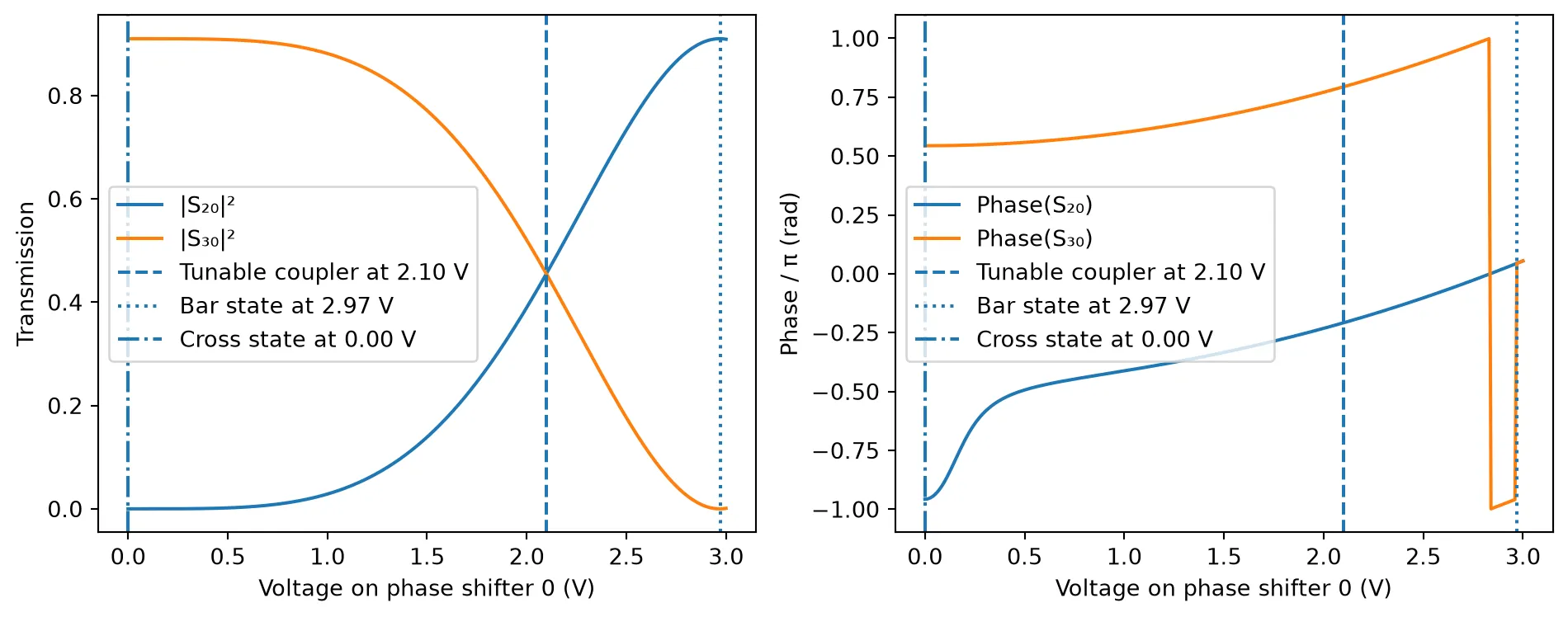
Unit Cell
Section titled “Unit Cell”Before constructing our main hexagonal programmable photonic circuit, we first define a unit cell composed of three interconnected tunable units. Each tunable unit (previously defined) functions as an independently configurable element, and this unit cell serves as the building block for assembling larger, more complex programmable structures.
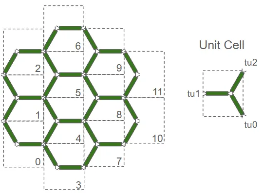
# Define netlist for creating a unit cell composed of three tunable unitsnetlist_uc = {    "name": "Unit Cell",    "instances": {        "tu0": {  # bottom tunable unit            "component": tunable_unit,            "origin": (0, -1.5 * vertical_distance),        },        "tu1": {  # middle tunable unit            "component": tunable_unit,            "origin": (bul, 0),        },        "tu2": {  # top tunable unit            "component": tunable_unit,            "origin": (0, 1.5 * vertical_distance),        },    },    # Automatically route connections between tunable units    "routes": [        (("tu1", "P0"), ("tu0", "P2"), pf.parametric.route),        (("tu0", "P3"), ("tu2", "P2"), pf.parametric.route),        (("tu1", "P1"), ("tu2", "P3"), pf.parametric.route),    ],    # External ports definition for further connectivity    "ports": [        ("tu0", "P0"),        ("tu0", "P1"),        ("tu2", "P0"),        ("tu2", "P1"),        ("tu1", "P2"),        ("tu1", "P3"),    ],    # Circuit model assigned to the unit cell    "models": [(pf.CircuitModel(), "Circuit")],}
# Create the unit cell component from the defined netlistunit_cell = pf.component_from_netlist(netlist_uc)
# Visualize the assembled unit cellviewer(unit_cell);fill:%23221f20;font-weight:bold;font-size:10.950240px;}.terminal{fill:none;stroke:%23805080;stroke-width:1.368780;}.dashed{stroke-dasharray:6.843900,4.106340;}.port{fill:none;stroke:%23805080;stroke-width:2.737560;}.virtual-connection{fill:none;stroke:%23907090;stroke-width:2.053170;}.layer_31_0{stroke:%238c78ef;fill:url(%23pat-layer_31_0);fill-opacity:0.492;}.label_31_0{fill:%238c78ef;}.layer_33_0{stroke:%238c78ef;fill:url(%23pat-layer_33_0);fill-opacity:0.492;}.label_33_0{fill:%238c78ef;}.layer_102_0{stroke:%238c78ef;fill:url(%23pat-layer_102_0);fill-opacity:0.492;}.label_102_0{fill:%238c78ef;}.layer_110_0{stroke:%238c78ef;fill:url(%23pat-layer_110_0);fill-opacity:0.492;}.label_110_0{fill:%238c78ef;}.layer_189_0{stroke:%23000000;fill:none;}.label_189_0{fill:%23000000;}.layer_201_0{stroke:%2300ee00;fill:url(%23pat-layer_201_0);fill-opacity:0.492;}.label_201_0{fill:%2300ee00;}.layer_401_0{stroke:%236a8ad2;fill:url(%23pat-layer_401_0);fill-opacity:0.492;}.label_401_0{fill:%236a8ad2;}.layer_202_0{stroke:%23007600;fill:url(%23pat-layer_202_0);fill-opacity:0.492;}.label_202_0{fill:%23007600;}.layer_68_0{stroke:%23008000;fill:url(%23pat-layer_68_0);fill-opacity:0.492;}.label_68_0{fill:%23008000;}.layer_5_0{stroke:%236a8ad2;fill:url(%23pat-layer_5_0);fill-opacity:0.492;}.label_5_0{fill:%236a8ad2;}.layer_998_0{stroke:%23000000;fill:none;}.label_998_0{fill:%23000000;}.layer_312_1{stroke:%2300b8b8;fill:url(%23pat-layer_312_1);fill-opacity:0.492;}.label_312_1{fill:%2300b8b8;}.layer_312_0{stroke:%2300b8b8;fill:url(%23pat-layer_312_0);fill-opacity:0.492;}.label_312_0{fill:%2300b8b8;}.layer_402_0{stroke:%23ff0000;fill:url(%23pat-layer_402_0);fill-opacity:0.492;}.label_402_0{fill:%23ff0000;}.layer_401_4{stroke:%236a8ad2;fill:url(%23pat-layer_401_4);fill-opacity:0.492;}.label_401_4{fill:%236a8ad2;}.layer_389_0{stroke:%23ff00ff;fill:url(%23pat-layer_389_0);fill-opacity:0.492;}.label_389_0{fill:%23ff00ff;}.layer_402_1{stroke:%23ff0000;fill:url(%23pat-layer_402_1);fill-opacity:0.492;}.label_402_1{fill:%23ff0000;}.layer_350_1{stroke:%23697a00;fill:url(%23pat-layer_350_1);fill-opacity:0.492;}.label_350_1{fill:%23697a00;}.layer_401_1{stroke:%236a8ad2;fill:url(%23pat-layer_401_1);fill-opacity:0.492;}.label_401_1{fill:%236a8ad2;}.layer_313_2{stroke:%2301d95b;fill:url(%23pat-layer_313_2);fill-opacity:0.492;}.label_313_2{fill:%2301d95b;}.layer_313_1{stroke:%2301d95b;fill:url(%23pat-layer_313_1);fill-opacity:0.492;}.label_313_1{fill:%2301d95b;}.layer_313_0{stroke:%2301d95b;fill:url(%23pat-layer_313_0);fill-opacity:0.492;}.label_313_0{fill:%2301d95b;}.layer_400_0{stroke:%23a96868;fill:url(%23pat-layer_400_0);fill-opacity:0.492;}.label_400_0{fill:%23a96868;}.layer_312_3{stroke:%2300b8b8;fill:url(%23pat-layer_312_3);fill-opacity:0.492;}.label_312_3{fill:%2300b8b8;}.layer_389_1{stroke:%23ff00ff;fill:url(%23pat-layer_389_1);fill-opacity:0.492;}.label_389_1{fill:%23ff00ff;}.layer_401_3{stroke:%236a8ad2;fill:url(%23pat-layer_401_3);fill-opacity:0.492;}.label_401_3{fill:%236a8ad2;}.layer_403_2{stroke:%23500080;fill:url(%23pat-layer_403_2);fill-opacity:0.492;}.label_403_2{fill:%23500080;}.layer_403_3{stroke:%23500080;fill:url(%23pat-layer_403_3);fill-opacity:0.492;}.label_403_3{fill:%23500080;}.layer_403_1{stroke:%23500080;fill:url(%23pat-layer_403_1);fill-opacity:0.492;}.label_403_1{fill:%23500080;}.layer_403_0{stroke:%23500080;fill:url(%23pat-layer_403_0);fill-opacity:0.492;}.label_403_0{fill:%23500080;}.layer_311_1{stroke:%23ac6c56;fill:url(%23pat-layer_311_1);fill-opacity:0.492;}.label_311_1{fill:%23ac6c56;}.layer_311_0{stroke:%23ac6c56;fill:url(%23pat-layer_311_0);fill-opacity:0.492;}.label_311_0{fill:%23ac6c56;}.layer_301_1{stroke:%23800057;fill:url(%23pat-layer_301_1);fill-opacity:0.492;}.label_301_1{fill:%23800057;}.layer_301_0{stroke:%23800057;fill:url(%23pat-layer_301_0);fill-opacity:0.492;}.label_301_0{fill:%23800057;}.layer_305_1{stroke:%23808080;fill:url(%23pat-layer_305_1);fill-opacity:0.492;}.label_305_1{fill:%23808080;}.layer_305_0{stroke:%23808080;fill:url(%23pat-layer_305_0);fill-opacity:0.492;}.label_305_0{fill:%23808080;}.layer_999_0{stroke:%230000ff;fill:url(%23pat-layer_999_0);fill-opacity:0.492;}.label_999_0{fill:%230000ff;}.layer_81_0{stroke:%23808080;fill:url(%23pat-layer_81_0);fill-opacity:0.492;}.label_81_0{fill:%23808080;}.layer_290_0{stroke:%23a46eda;fill:none;}.label_290_0{fill:%23a46eda;}.layer_205_0{stroke:%2349b203;fill:url(%23pat-layer_205_0);fill-opacity:0.492;}.label_205_0{fill:%2349b203;}.layer_11_0{stroke:%230000ff;fill:url(%23pat-layer_11_0);fill-opacity:0.492;}.label_11_0{fill:%230000ff;}.layer_12_0{stroke:%23a57b00;fill:url(%23pat-layer_12_0);fill-opacity:0.492;}.label_12_0{fill:%23a57b00;}.layer_13_0{stroke:%23800057;fill:url(%23pat-layer_13_0);fill-opacity:0.492;}.label_13_0{fill:%23800057;}.layer_6_0{stroke:%23ff0000;fill:url(%23pat-layer_6_0);fill-opacity:0.492;}.label_6_0{fill:%23ff0000;}.layer_1_10{stroke:%23c96585;fill:url(%23pat-layer_1_10);fill-opacity:0.492;}.label_1_10{fill:%23c96585;}.layer_1_11{stroke:%23800000;fill:url(%23pat-layer_1_11);fill-opacity:0.492;}.label_1_11{fill:%23800000;}.layer_200_0{stroke:%23ff0000;fill:url(%23pat-layer_200_0);fill-opacity:0.492;}.label_200_0{fill:%23ff0000;}.layer_1_0{stroke:%23c96585;fill:url(%23pat-layer_1_0);fill-opacity:0.492;}.label_1_0{fill:%23c96585;}.layer_2_0{stroke:%23a46eda;fill:url(%23pat-layer_2_0);fill-opacity:0.492;}.label_2_0{fill:%23a46eda;}.layer_20_0{stroke:%2353793d;fill:url(%23pat-layer_20_0);fill-opacity:0.492;}.label_20_0{fill:%2353793d;}.layer_22_0{stroke:%23ec7600;fill:url(%23pat-layer_22_0);fill-opacity:0.492;}.label_22_0{fill:%23ec7600;}.layer_24_0{stroke:%2300b8b8;fill:url(%23pat-layer_24_0);fill-opacity:0.492;}.label_24_0{fill:%2300b8b8;}.layer_21_0{stroke:%23736264;fill:url(%23pat-layer_21_0);fill-opacity:0.492;}.label_21_0{fill:%23736264;}.layer_23_0{stroke:%23697a00;fill:url(%23pat-layer_23_0);fill-opacity:0.492;}.label_23_0{fill:%23697a00;}.layer_25_0{stroke:%23008000;fill:url(%23pat-layer_25_0);fill-opacity:0.492;}.label_25_0{fill:%23008000;}.layer_350_0{stroke:%23697a00;fill:url(%23pat-layer_350_0);fill-opacity:0.492;}.label_350_0{fill:%23697a00;}.layer_10_0{stroke:%23000000;fill:none;}.label_10_0{fill:%23000000;}.layer_203_0{stroke:%23008000;fill:url(%23pat-layer_203_0);fill-opacity:0.492;}.label_203_0{fill:%23008000;}.layer_40_0{stroke:%230000ff;fill:url(%23pat-layer_40_0);fill-opacity:0.492;}.label_40_0{fill:%230000ff;}.layer_401_2{stroke:%236a8ad2;fill:url(%23pat-layer_401_2);fill-opacity:0.492;}.label_401_2{fill:%236a8ad2;}.layer_301_2{stroke:%23800057;fill:url(%23pat-layer_301_2);fill-opacity:0.492;}.label_301_2{fill:%23800057;}</style><defs><path id=%22port-symbol%22 class=%22port%22 d=%22M 0,-5.475120 L 8.212680,0 0,5.475120%22 /><path id=%22ref-port-symbol%22 class=%22port%22 style=%22stroke-opacity:0.33;%22 d=%22M 0,-4.106340 C 5.475120,-4.106340 5.475120,4.106340 0,4.106340%22 /><circle id=%22port-bend-symbol%22 style=%22stroke-width:0;stroke:none;fill:%23805080;fill-opacity:1;%22 cx=%220%22 cy=%220%22 r=%222.463804%22 /><circle id=%22connection-symbol%22 style=%22stroke-width:0;stroke:none;fill:%23907090;fill-opacity:1;%22 cx=%220%22 cy=%220%22 r=%222.874438%22 /><pattern id=%22pat-layer_31_0%22 patternUnits=%22userSpaceOnUse%22 width=%226.843900%22 height=%226.843900%22 patternTransform=%22translate(5.233571,6.483695)%22><line x1=%220%22 y1=%220%22 x2=%226.843900%22 y2=%226.843900%22 style=%22stroke:%238c78ef;stroke-width:0.684390%22 /><line x1=%22-3.421950%22 y1=%223.421950%22 x2=%223.421950%22 y2=%2210.265850%22 style=%22stroke:%238c78ef;stroke-width:0.684390%22 /><line x1=%223.421950%22 y1=%22-3.421950%22 x2=%2210.265850%22 y2=%223.421950%22 style=%22stroke:%238c78ef;stroke-width:0.684390%22 /></pattern><pattern id=%22pat-layer_33_0%22 patternUnits=%22userSpaceOnUse%22 width=%226.843900%22 height=%226.843900%22 patternTransform=%22translate(4.025824,0.720411)%22><line x1=%220%22 y1=%220%22 x2=%226.843900%22 y2=%226.843900%22 style=%22stroke:%238c78ef;stroke-width:0.684390%22 /><line x1=%22-3.421950%22 y1=%223.421950%22 x2=%223.421950%22 y2=%2210.265850%22 style=%22stroke:%238c78ef;stroke-width:0.684390%22 /><line x1=%223.421950%22 y1=%22-3.421950%22 x2=%2210.265850%22 y2=%223.421950%22 style=%22stroke:%238c78ef;stroke-width:0.684390%22 /></pattern><pattern id=%22pat-layer_102_0%22 patternUnits=%22userSpaceOnUse%22 width=%226.843900%22 height=%226.843900%22 patternTransform=%22translate(0.000000,0.360205)%22><line x1=%220%22 y1=%220%22 x2=%226.843900%22 y2=%226.843900%22 style=%22stroke:%238c78ef;stroke-width:0.684390%22 /><line x1=%22-3.421950%22 y1=%223.421950%22 x2=%223.421950%22 y2=%2210.265850%22 style=%22stroke:%238c78ef;stroke-width:0.684390%22 /><line x1=%223.421950%22 y1=%22-3.421950%22 x2=%2210.265850%22 y2=%223.421950%22 style=%22stroke:%238c78ef;stroke-width:0.684390%22 /></pattern><pattern id=%22pat-layer_110_0%22 patternUnits=%22userSpaceOnUse%22 width=%226.843900%22 height=%226.843900%22 patternTransform=%22translate(2.012912,4.682668)%22><line x1=%220%22 y1=%220%22 x2=%226.843900%22 y2=%226.843900%22 style=%22stroke:%238c78ef;stroke-width:0.684390%22 /><line x1=%22-3.421950%22 y1=%223.421950%22 x2=%223.421950%22 y2=%2210.265850%22 style=%22stroke:%238c78ef;stroke-width:0.684390%22 /><line x1=%223.421950%22 y1=%22-3.421950%22 x2=%2210.265850%22 y2=%223.421950%22 style=%22stroke:%238c78ef;stroke-width:0.684390%22 /></pattern><pattern id=%22pat-layer_201_0%22 patternUnits=%22userSpaceOnUse%22 width=%226.843900%22 height=%226.843900%22 patternTransform=%22translate(5.233571,2.521437)%22><circle cx=%223.421950%22 cy=%223.421950%22 r=%220.684390%22 style=%22stroke:none;fill:%2300ee00;fill-opacity:1.0%22 /></pattern><pattern id=%22pat-layer_401_0%22 patternUnits=%22userSpaceOnUse%22 width=%224.106340%22 height=%224.106340%22 patternTransform=%22translate(0.483099,0.648369)%22><line x1=%220%22 y1=%220%22 x2=%224.106340%22 y2=%224.106340%22 style=%22stroke:%236a8ad2;stroke-width:0.684390%22 /><line x1=%22-2.053170%22 y1=%222.053170%22 x2=%222.053170%22 y2=%226.159510%22 style=%22stroke:%236a8ad2;stroke-width:0.684390%22 /><line x1=%222.053170%22 y1=%22-2.053170%22 x2=%226.159510%22 y2=%222.053170%22 style=%22stroke:%236a8ad2;stroke-width:0.684390%22 /><line x1=%224.106340%22 y1=%220%22 x2=%220%22 y2=%224.106340%22 style=%22stroke:%236a8ad2;stroke-width:0.684390%22 /><line x1=%226.159510%22 y1=%222.053170%22 x2=%222.053170%22 y2=%226.159510%22 style=%22stroke:%236a8ad2;stroke-width:0.684390%22 /><line x1=%222.053170%22 y1=%22-2.053170%22 x2=%22-2.053170%22 y2=%222.053170%22 style=%22stroke:%236a8ad2;stroke-width:0.684390%22 /></pattern><pattern id=%22pat-layer_202_0%22 patternUnits=%22userSpaceOnUse%22 width=%224.106340%22 height=%224.106340%22 patternTransform=%22translate(0.724648,3.890217)%22><circle cx=%222.053170%22 cy=%222.053170%22 r=%220.684390%22 style=%22stroke:none;fill:%23007600;fill-opacity:1.0%22 /></pattern><pattern id=%22pat-layer_68_0%22 patternUnits=%22userSpaceOnUse%22 width=%226.843900%22 height=%226.843900%22 patternTransform=%22translate(0.000000,2.521437)%22><circle cx=%223.421950%22 cy=%223.421950%22 r=%220.684390%22 style=%22stroke:none;fill:%23008000;fill-opacity:1.0%22 /></pattern><pattern id=%22pat-layer_5_0%22 patternUnits=%22userSpaceOnUse%22 width=%224.106340%22 height=%224.106340%22 patternTransform=%22translate(0.241549,3.674094)%22><line x1=%222.053170%22 y1=%220%22 x2=%222.053170%22 y2=%224.106340%22 style=%22stroke:%236a8ad2;stroke-width:0.684390%22 /></pattern><pattern id=%22pat-layer_312_1%22 patternUnits=%22userSpaceOnUse%22 width=%224.106340%22 height=%224.106340%22 patternTransform=%22translate(0.966198,3.241847)%22><line x1=%220%22 y1=%220%22 x2=%224.106340%22 y2=%224.106340%22 style=%22stroke:%2300b8b8;stroke-width:0.684390%22 /><line x1=%22-2.053170%22 y1=%222.053170%22 x2=%222.053170%22 y2=%226.159510%22 style=%22stroke:%2300b8b8;stroke-width:0.684390%22 /><line x1=%222.053170%22 y1=%22-2.053170%22 x2=%226.159510%22 y2=%222.053170%22 style=%22stroke:%2300b8b8;stroke-width:0.684390%22 /></pattern><pattern id=%22pat-layer_312_0%22 patternUnits=%22userSpaceOnUse%22 width=%226.843900%22 height=%226.843900%22 patternTransform=%22translate(3.220659,4.322463)%22><line x1=%223.421950%22 y1=%220%22 x2=%223.421950%22 y2=%226.843900%22 style=%22stroke:%2300b8b8;stroke-width:0.684390%22 /></pattern><pattern id=%22pat-layer_402_0%22 patternUnits=%22userSpaceOnUse%22 width=%226.843900%22 height=%226.843900%22 patternTransform=%22translate(3.623241,5.042874)%22><line x1=%223.421950%22 y1=%220%22 x2=%223.421950%22 y2=%226.843900%22 style=%22stroke:%23ff0000;stroke-width:0.684390%22 /><line x1=%220%22 y1=%223.421950%22 x2=%226.843900%22 y2=%223.421950%22 style=%22stroke:%23ff0000;stroke-width:0.684390%22 /></pattern><pattern id=%22pat-layer_401_4%22 patternUnits=%22userSpaceOnUse%22 width=%224.106340%22 height=%224.106340%22 patternTransform=%22translate(0.724648,3.241847)%22><line x1=%222.053170%22 y1=%220%22 x2=%222.053170%22 y2=%224.106340%22 style=%22stroke:%236a8ad2;stroke-width:0.684390%22 /></pattern><pattern id=%22pat-layer_389_0%22 patternUnits=%22userSpaceOnUse%22 width=%224.106340%22 height=%224.106340%22 patternTransform=%22translate(0.724648,0.864493)%22><line x1=%222.053170%22 y1=%220%22 x2=%222.053170%22 y2=%224.106340%22 style=%22stroke:%23ff00ff;stroke-width:0.684390%22 /><line x1=%220%22 y1=%222.053170%22 x2=%224.106340%22 y2=%222.053170%22 style=%22stroke:%23ff00ff;stroke-width:0.684390%22 /></pattern><pattern id=%22pat-layer_402_1%22 patternUnits=%22userSpaceOnUse%22 width=%224.106340%22 height=%224.106340%22 patternTransform=%22translate(1.207747,3.674094)%22><line x1=%220%22 y1=%220%22 x2=%224.106340%22 y2=%224.106340%22 style=%22stroke:%23ff0000;stroke-width:0.684390%22 /><line x1=%22-2.053170%22 y1=%222.053170%22 x2=%222.053170%22 y2=%226.159510%22 style=%22stroke:%23ff0000;stroke-width:0.684390%22 /><line x1=%222.053170%22 y1=%22-2.053170%22 x2=%226.159510%22 y2=%222.053170%22 style=%22stroke:%23ff0000;stroke-width:0.684390%22 /><line x1=%224.106340%22 y1=%220%22 x2=%220%22 y2=%224.106340%22 style=%22stroke:%23ff0000;stroke-width:0.684390%22 /><line x1=%226.159510%22 y1=%222.053170%22 x2=%222.053170%22 y2=%226.159510%22 style=%22stroke:%23ff0000;stroke-width:0.684390%22 /><line x1=%222.053170%22 y1=%22-2.053170%22 x2=%22-2.053170%22 y2=%222.053170%22 style=%22stroke:%23ff0000;stroke-width:0.684390%22 /></pattern><pattern id=%22pat-layer_350_1%22 patternUnits=%22userSpaceOnUse%22 width=%224.106340%22 height=%224.106340%22 patternTransform=%22translate(3.623241,3.241847)%22><circle cx=%222.053170%22 cy=%222.053170%22 r=%220.684390%22 style=%22stroke:none;fill:%23697a00;fill-opacity:1.0%22 /></pattern><pattern id=%22pat-layer_401_1%22 patternUnits=%22userSpaceOnUse%22 width=%226.843900%22 height=%226.843900%22 patternTransform=%22translate(6.038735,2.161232)%22><line x1=%220%22 y1=%220%22 x2=%226.843900%22 y2=%226.843900%22 style=%22stroke:%236a8ad2;stroke-width:0.684390%22 /><line x1=%22-3.421950%22 y1=%223.421950%22 x2=%223.421950%22 y2=%2210.265850%22 style=%22stroke:%236a8ad2;stroke-width:0.684390%22 /><line x1=%223.421950%22 y1=%22-3.421950%22 x2=%2210.265850%22 y2=%223.421950%22 style=%22stroke:%236a8ad2;stroke-width:0.684390%22 /><line x1=%226.843900%22 y1=%220%22 x2=%220%22 y2=%226.843900%22 style=%22stroke:%236a8ad2;stroke-width:0.684390%22 /><line x1=%2210.265850%22 y1=%223.421950%22 x2=%223.421950%22 y2=%2210.265850%22 style=%22stroke:%236a8ad2;stroke-width:0.684390%22 /><line x1=%223.421950%22 y1=%22-3.421950%22 x2=%22-3.421950%22 y2=%223.421950%22 style=%22stroke:%236a8ad2;stroke-width:0.684390%22 /></pattern><pattern id=%22pat-layer_313_2%22 patternUnits=%22userSpaceOnUse%22 width=%224.106340%22 height=%224.106340%22 patternTransform=%22translate(1.690846,2.161232)%22><line x1=%220%22 y1=%220%22 x2=%224.106340%22 y2=%224.106340%22 style=%22stroke:%2301d95b;stroke-width:0.684390%22 /><line x1=%22-2.053170%22 y1=%222.053170%22 x2=%222.053170%22 y2=%226.159510%22 style=%22stroke:%2301d95b;stroke-width:0.684390%22 /><line x1=%222.053170%22 y1=%22-2.053170%22 x2=%226.159510%22 y2=%222.053170%22 style=%22stroke:%2301d95b;stroke-width:0.684390%22 /></pattern><pattern id=%22pat-layer_313_1%22 patternUnits=%22userSpaceOnUse%22 width=%226.843900%22 height=%226.843900%22 patternTransform=%22translate(4.428406,2.521437)%22><line x1=%223.421950%22 y1=%220%22 x2=%223.421950%22 y2=%226.843900%22 style=%22stroke:%2301d95b;stroke-width:0.684390%22 /></pattern><pattern id=%22pat-layer_313_0%22 patternUnits=%22userSpaceOnUse%22 width=%224.106340%22 height=%224.106340%22 patternTransform=%22translate(3.623241,0.864493)%22><line x1=%222.053170%22 y1=%220%22 x2=%222.053170%22 y2=%224.106340%22 style=%22stroke:%2301d95b;stroke-width:0.684390%22 /></pattern><pattern id=%22pat-layer_400_0%22 patternUnits=%22userSpaceOnUse%22 width=%226.843900%22 height=%226.843900%22 patternTransform=%22translate(4.830988,3.962258)%22><line x1=%220%22 y1=%220%22 x2=%226.843900%22 y2=%226.843900%22 style=%22stroke:%23a96868;stroke-width:0.684390%22 /><line x1=%22-3.421950%22 y1=%223.421950%22 x2=%223.421950%22 y2=%2210.265850%22 style=%22stroke:%23a96868;stroke-width:0.684390%22 /><line x1=%223.421950%22 y1=%22-3.421950%22 x2=%2210.265850%22 y2=%223.421950%22 style=%22stroke:%23a96868;stroke-width:0.684390%22 /><line x1=%226.843900%22 y1=%220%22 x2=%220%22 y2=%226.843900%22 style=%22stroke:%23a96868;stroke-width:0.684390%22 /><line x1=%2210.265850%22 y1=%223.421950%22 x2=%223.421950%22 y2=%2210.265850%22 style=%22stroke:%23a96868;stroke-width:0.684390%22 /><line x1=%223.421950%22 y1=%22-3.421950%22 x2=%22-3.421950%22 y2=%223.421950%22 style=%22stroke:%23a96868;stroke-width:0.684390%22 /></pattern><pattern id=%22pat-layer_312_3%22 patternUnits=%22userSpaceOnUse%22 width=%224.106340%22 height=%224.106340%22 patternTransform=%22translate(3.140142,0.432246)%22><line x1=%224.106340%22 y1=%220%22 x2=%220%22 y2=%224.106340%22 style=%22stroke:%2300b8b8;stroke-width:0.684390%22 /><line x1=%226.159510%22 y1=%222.053170%22 x2=%222.053170%22 y2=%226.159510%22 style=%22stroke:%2300b8b8;stroke-width:0.684390%22 /><line x1=%222.053170%22 y1=%22-2.053170%22 x2=%22-2.053170%22 y2=%222.053170%22 style=%22stroke:%2300b8b8;stroke-width:0.684390%22 /></pattern><pattern id=%22pat-layer_389_1%22 patternUnits=%22userSpaceOnUse%22 width=%226.843900%22 height=%226.843900%22 patternTransform=%22translate(6.441318,2.521437)%22><line x1=%223.421950%22 y1=%220%22 x2=%223.421950%22 y2=%226.843900%22 style=%22stroke:%23ff00ff;stroke-width:0.684390%22 /><line x1=%220%22 y1=%223.421950%22 x2=%226.843900%22 y2=%223.421950%22 style=%22stroke:%23ff00ff;stroke-width:0.684390%22 /></pattern><pattern id=%22pat-layer_401_3%22 patternUnits=%22userSpaceOnUse%22 width=%226.843900%22 height=%226.843900%22 patternTransform=%22translate(2.818076,4.322463)%22><line x1=%220%22 y1=%223.421950%22 x2=%226.843900%22 y2=%223.421950%22 style=%22stroke:%236a8ad2;stroke-width:0.684390%22 /></pattern><pattern id=%22pat-layer_403_2%22 patternUnits=%22userSpaceOnUse%22 width=%224.106340%22 height=%224.106340%22 patternTransform=%22translate(1.932395,2.593478)%22><line x1=%220%22 y1=%220%22 x2=%224.106340%22 y2=%224.106340%22 style=%22stroke:%23500080;stroke-width:0.684390%22 /><line x1=%22-2.053170%22 y1=%222.053170%22 x2=%222.053170%22 y2=%226.159510%22 style=%22stroke:%23500080;stroke-width:0.684390%22 /><line x1=%222.053170%22 y1=%22-2.053170%22 x2=%226.159510%22 y2=%222.053170%22 style=%22stroke:%23500080;stroke-width:0.684390%22 /><line x1=%224.106340%22 y1=%220%22 x2=%220%22 y2=%224.106340%22 style=%22stroke:%23500080;stroke-width:0.684390%22 /><line x1=%226.159510%22 y1=%222.053170%22 x2=%222.053170%22 y2=%226.159510%22 style=%22stroke:%23500080;stroke-width:0.684390%22 /><line x1=%222.053170%22 y1=%22-2.053170%22 x2=%22-2.053170%22 y2=%222.053170%22 style=%22stroke:%23500080;stroke-width:0.684390%22 /></pattern><pattern id=%22pat-layer_403_3%22 patternUnits=%22userSpaceOnUse%22 width=%226.843900%22 height=%226.843900%22 patternTransform=%22translate(1.610329,5.403079)%22><line x1=%220%22 y1=%220%22 x2=%226.843900%22 y2=%226.843900%22 style=%22stroke:%23500080;stroke-width:0.684390%22 /><line x1=%22-3.421950%22 y1=%223.421950%22 x2=%223.421950%22 y2=%2210.265850%22 style=%22stroke:%23500080;stroke-width:0.684390%22 /><line x1=%223.421950%22 y1=%22-3.421950%22 x2=%2210.265850%22 y2=%223.421950%22 style=%22stroke:%23500080;stroke-width:0.684390%22 /><line x1=%226.843900%22 y1=%220%22 x2=%220%22 y2=%226.843900%22 style=%22stroke:%23500080;stroke-width:0.684390%22 /><line x1=%2210.265850%22 y1=%223.421950%22 x2=%223.421950%22 y2=%2210.265850%22 style=%22stroke:%23500080;stroke-width:0.684390%22 /><line x1=%223.421950%22 y1=%22-3.421950%22 x2=%22-3.421950%22 y2=%223.421950%22 style=%22stroke:%23500080;stroke-width:0.684390%22 /></pattern><pattern id=%22pat-layer_403_1%22 patternUnits=%22userSpaceOnUse%22 width=%226.843900%22 height=%226.843900%22 patternTransform=%22translate(4.830988,3.241847)%22><line x1=%223.421950%22 y1=%220%22 x2=%223.421950%22 y2=%226.843900%22 style=%22stroke:%23500080;stroke-width:0.684390%22 /><line x1=%220%22 y1=%223.421950%22 x2=%226.843900%22 y2=%223.421950%22 style=%22stroke:%23500080;stroke-width:0.684390%22 /></pattern><pattern id=%22pat-layer_403_0%22 patternUnits=%22userSpaceOnUse%22 width=%224.106340%22 height=%224.106340%22 patternTransform=%22translate(3.864791,1.296739)%22><line x1=%222.053170%22 y1=%220%22 x2=%222.053170%22 y2=%224.106340%22 style=%22stroke:%23500080;stroke-width:0.684390%22 /><line x1=%220%22 y1=%222.053170%22 x2=%224.106340%22 y2=%222.053170%22 style=%22stroke:%23500080;stroke-width:0.684390%22 /></pattern><pattern id=%22pat-layer_311_1%22 patternUnits=%22userSpaceOnUse%22 width=%226.843900%22 height=%226.843900%22 patternTransform=%22translate(5.636153,1.440821)%22><line x1=%220%22 y1=%220%22 x2=%226.843900%22 y2=%226.843900%22 style=%22stroke:%23ac6c56;stroke-width:0.684390%22 /><line x1=%22-3.421950%22 y1=%223.421950%22 x2=%223.421950%22 y2=%2210.265850%22 style=%22stroke:%23ac6c56;stroke-width:0.684390%22 /><line x1=%223.421950%22 y1=%22-3.421950%22 x2=%2210.265850%22 y2=%223.421950%22 style=%22stroke:%23ac6c56;stroke-width:0.684390%22 /></pattern><pattern id=%22pat-layer_311_0%22 patternUnits=%22userSpaceOnUse%22 width=%224.106340%22 height=%224.106340%22 patternTransform=%22translate(0.241549,0.216123)%22><line x1=%220%22 y1=%220%22 x2=%224.106340%22 y2=%224.106340%22 style=%22stroke:%23ac6c56;stroke-width:0.684390%22 /><line x1=%22-2.053170%22 y1=%222.053170%22 x2=%222.053170%22 y2=%226.159510%22 style=%22stroke:%23ac6c56;stroke-width:0.684390%22 /><line x1=%222.053170%22 y1=%22-2.053170%22 x2=%226.159510%22 y2=%222.053170%22 style=%22stroke:%23ac6c56;stroke-width:0.684390%22 /></pattern><pattern id=%22pat-layer_301_1%22 patternUnits=%22userSpaceOnUse%22 width=%226.843900%22 height=%226.843900%22 patternTransform=%22translate(4.830988,2.881642)%22><line x1=%220%22 y1=%223.421950%22 x2=%226.843900%22 y2=%223.421950%22 style=%22stroke:%23800057;stroke-width:0.684390%22 /></pattern><pattern id=%22pat-layer_301_0%22 patternUnits=%22userSpaceOnUse%22 width=%224.106340%22 height=%224.106340%22 patternTransform=%22translate(3.864791,1.080616)%22><line x1=%220%22 y1=%222.053170%22 x2=%224.106340%22 y2=%222.053170%22 style=%22stroke:%23800057;stroke-width:0.684390%22 /></pattern><pattern id=%22pat-layer_305_1%22 patternUnits=%22userSpaceOnUse%22 width=%226.843900%22 height=%226.843900%22 patternTransform=%22translate(2.415494,5.042874)%22><line x1=%223.421950%22 y1=%220%22 x2=%223.421950%22 y2=%226.843900%22 style=%22stroke:%23808080;stroke-width:0.684390%22 /><line x1=%220%22 y1=%223.421950%22 x2=%226.843900%22 y2=%223.421950%22 style=%22stroke:%23808080;stroke-width:0.684390%22 /></pattern><pattern id=%22pat-layer_305_0%22 patternUnits=%22userSpaceOnUse%22 width=%224.106340%22 height=%224.106340%22 patternTransform=%22translate(2.415494,2.377355)%22><line x1=%222.053170%22 y1=%220%22 x2=%222.053170%22 y2=%224.106340%22 style=%22stroke:%23808080;stroke-width:0.684390%22 /><line x1=%220%22 y1=%222.053170%22 x2=%224.106340%22 y2=%222.053170%22 style=%22stroke:%23808080;stroke-width:0.684390%22 /></pattern><pattern id=%22pat-layer_999_0%22 patternUnits=%22userSpaceOnUse%22 width=%224.106340%22 height=%224.106340%22 patternTransform=%22translate(1.449296,1.512862)%22><line x1=%222.053170%22 y1=%220%22 x2=%222.053170%22 y2=%224.106340%22 style=%22stroke:%230000ff;stroke-width:0.684390%22 /></pattern><pattern id=%22pat-layer_81_0%22 patternUnits=%22userSpaceOnUse%22 width=%224.106340%22 height=%224.106340%22 patternTransform=%22translate(1.449296,3.674094)%22><line x1=%222.053170%22 y1=%220%22 x2=%222.053170%22 y2=%224.106340%22 style=%22stroke:%23808080;stroke-width:0.684390%22 /><line x1=%220%22 y1=%222.053170%22 x2=%224.106340%22 y2=%222.053170%22 style=%22stroke:%23808080;stroke-width:0.684390%22 /></pattern><pattern id=%22pat-layer_205_0%22 patternUnits=%22userSpaceOnUse%22 width=%224.106340%22 height=%224.106340%22 patternTransform=%22translate(1.690846,2.809601)%22><line x1=%220%22 y1=%220%22 x2=%224.106340%22 y2=%224.106340%22 style=%22stroke:%2349b203;stroke-width:0.684390%22 /><line x1=%22-2.053170%22 y1=%222.053170%22 x2=%222.053170%22 y2=%226.159510%22 style=%22stroke:%2349b203;stroke-width:0.684390%22 /><line x1=%222.053170%22 y1=%22-2.053170%22 x2=%226.159510%22 y2=%222.053170%22 style=%22stroke:%2349b203;stroke-width:0.684390%22 /><line x1=%224.106340%22 y1=%220%22 x2=%220%22 y2=%224.106340%22 style=%22stroke:%2349b203;stroke-width:0.684390%22 /><line x1=%226.159510%22 y1=%222.053170%22 x2=%222.053170%22 y2=%226.159510%22 style=%22stroke:%2349b203;stroke-width:0.684390%22 /><line x1=%222.053170%22 y1=%22-2.053170%22 x2=%22-2.053170%22 y2=%222.053170%22 style=%22stroke:%2349b203;stroke-width:0.684390%22 /></pattern><pattern id=%22pat-layer_11_0%22 patternUnits=%22userSpaceOnUse%22 width=%224.106340%22 height=%224.106340%22 patternTransform=%22translate(2.173945,1.512862)%22><line x1=%224.106340%22 y1=%220%22 x2=%220%22 y2=%224.106340%22 style=%22stroke:%230000ff;stroke-width:0.684390%22 /><line x1=%226.159510%22 y1=%222.053170%22 x2=%222.053170%22 y2=%226.159510%22 style=%22stroke:%230000ff;stroke-width:0.684390%22 /><line x1=%222.053170%22 y1=%22-2.053170%22 x2=%22-2.053170%22 y2=%222.053170%22 style=%22stroke:%230000ff;stroke-width:0.684390%22 /></pattern><pattern id=%22pat-layer_12_0%22 patternUnits=%22userSpaceOnUse%22 width=%224.106340%22 height=%224.106340%22 patternTransform=%22translate(3.864791,3.890217)%22><line x1=%220%22 y1=%220%22 x2=%224.106340%22 y2=%224.106340%22 style=%22stroke:%23a57b00;stroke-width:0.684390%22 /><line x1=%22-2.053170%22 y1=%222.053170%22 x2=%222.053170%22 y2=%226.159510%22 style=%22stroke:%23a57b00;stroke-width:0.684390%22 /><line x1=%222.053170%22 y1=%22-2.053170%22 x2=%226.159510%22 y2=%222.053170%22 style=%22stroke:%23a57b00;stroke-width:0.684390%22 /></pattern><pattern id=%22pat-layer_13_0%22 patternUnits=%22userSpaceOnUse%22 width=%224.106340%22 height=%224.106340%22 patternTransform=%22translate(1.449296,2.161232)%22><line x1=%224.106340%22 y1=%220%22 x2=%220%22 y2=%224.106340%22 style=%22stroke:%23800057;stroke-width:0.684390%22 /><line x1=%226.159510%22 y1=%222.053170%22 x2=%222.053170%22 y2=%226.159510%22 style=%22stroke:%23800057;stroke-width:0.684390%22 /><line x1=%222.053170%22 y1=%22-2.053170%22 x2=%22-2.053170%22 y2=%222.053170%22 style=%22stroke:%23800057;stroke-width:0.684390%22 /></pattern><pattern id=%22pat-layer_6_0%22 patternUnits=%22userSpaceOnUse%22 width=%226.843900%22 height=%226.843900%22 patternTransform=%22translate(3.220659,3.241847)%22><line x1=%220%22 y1=%223.421950%22 x2=%226.843900%22 y2=%223.421950%22 style=%22stroke:%23ff0000;stroke-width:0.684390%22 /></pattern><pattern id=%22pat-layer_1_10%22 patternUnits=%22userSpaceOnUse%22 width=%224.106340%22 height=%224.106340%22 patternTransform=%22translate(0.241549,0.648369)%22><line x1=%220%22 y1=%220%22 x2=%224.106340%22 y2=%224.106340%22 style=%22stroke:%23c96585;stroke-width:0.684390%22 /><line x1=%22-2.053170%22 y1=%222.053170%22 x2=%222.053170%22 y2=%226.159510%22 style=%22stroke:%23c96585;stroke-width:0.684390%22 /><line x1=%222.053170%22 y1=%22-2.053170%22 x2=%226.159510%22 y2=%222.053170%22 style=%22stroke:%23c96585;stroke-width:0.684390%22 /><line x1=%224.106340%22 y1=%220%22 x2=%220%22 y2=%224.106340%22 style=%22stroke:%23c96585;stroke-width:0.684390%22 /><line x1=%226.159510%22 y1=%222.053170%22 x2=%222.053170%22 y2=%226.159510%22 style=%22stroke:%23c96585;stroke-width:0.684390%22 /><line x1=%222.053170%22 y1=%22-2.053170%22 x2=%22-2.053170%22 y2=%222.053170%22 style=%22stroke:%23c96585;stroke-width:0.684390%22 /></pattern><pattern id=%22pat-layer_1_11%22 patternUnits=%22userSpaceOnUse%22 width=%226.843900%22 height=%226.843900%22 patternTransform=%22translate(5.636153,2.161232)%22><line x1=%223.421950%22 y1=%220%22 x2=%223.421950%22 y2=%226.843900%22 style=%22stroke:%23800000;stroke-width:0.684390%22 /><line x1=%220%22 y1=%223.421950%22 x2=%226.843900%22 y2=%223.421950%22 style=%22stroke:%23800000;stroke-width:0.684390%22 /></pattern><pattern id=%22pat-layer_200_0%22 patternUnits=%22userSpaceOnUse%22 width=%226.843900%22 height=%226.843900%22 patternTransform=%22translate(2.415494,5.403079)%22><line x1=%220%22 y1=%220%22 x2=%226.843900%22 y2=%226.843900%22 style=%22stroke:%23ff0000;stroke-width:0.684390%22 /><line x1=%22-3.421950%22 y1=%223.421950%22 x2=%223.421950%22 y2=%2210.265850%22 style=%22stroke:%23ff0000;stroke-width:0.684390%22 /><line x1=%223.421950%22 y1=%22-3.421950%22 x2=%2210.265850%22 y2=%223.421950%22 style=%22stroke:%23ff0000;stroke-width:0.684390%22 /><line x1=%226.843900%22 y1=%220%22 x2=%220%22 y2=%226.843900%22 style=%22stroke:%23ff0000;stroke-width:0.684390%22 /><line x1=%2210.265850%22 y1=%223.421950%22 x2=%223.421950%22 y2=%2210.265850%22 style=%22stroke:%23ff0000;stroke-width:0.684390%22 /><line x1=%223.421950%22 y1=%22-3.421950%22 x2=%22-3.421950%22 y2=%223.421950%22 style=%22stroke:%23ff0000;stroke-width:0.684390%22 /></pattern><pattern id=%22pat-layer_1_0%22 patternUnits=%22userSpaceOnUse%22 width=%224.106340%22 height=%224.106340%22 patternTransform=%22translate(1.690846,2.377355)%22><line x1=%224.106340%22 y1=%220%22 x2=%220%22 y2=%224.106340%22 style=%22stroke:%23c96585;stroke-width:0.684390%22 /><line x1=%226.159510%22 y1=%222.053170%22 x2=%222.053170%22 y2=%226.159510%22 style=%22stroke:%23c96585;stroke-width:0.684390%22 /><line x1=%222.053170%22 y1=%22-2.053170%22 x2=%22-2.053170%22 y2=%222.053170%22 style=%22stroke:%23c96585;stroke-width:0.684390%22 /></pattern><pattern id=%22pat-layer_2_0%22 patternUnits=%22userSpaceOnUse%22 width=%226.843900%22 height=%226.843900%22 patternTransform=%22translate(5.636153,1.080616)%22><line x1=%220%22 y1=%220%22 x2=%226.843900%22 y2=%226.843900%22 style=%22stroke:%23a46eda;stroke-width:0.684390%22 /><line x1=%22-3.421950%22 y1=%223.421950%22 x2=%223.421950%22 y2=%2210.265850%22 style=%22stroke:%23a46eda;stroke-width:0.684390%22 /><line x1=%223.421950%22 y1=%22-3.421950%22 x2=%2210.265850%22 y2=%223.421950%22 style=%22stroke:%23a46eda;stroke-width:0.684390%22 /></pattern><pattern id=%22pat-layer_20_0%22 patternUnits=%22userSpaceOnUse%22 width=%226.843900%22 height=%226.843900%22 patternTransform=%22translate(1.610329,3.962258)%22><line x1=%220%22 y1=%223.421950%22 x2=%226.843900%22 y2=%223.421950%22 style=%22stroke:%2353793d;stroke-width:0.684390%22 /></pattern><pattern id=%22pat-layer_22_0%22 patternUnits=%22userSpaceOnUse%22 width=%226.843900%22 height=%226.843900%22 patternTransform=%22translate(0.402582,5.042874)%22><line x1=%220%22 y1=%220%22 x2=%226.843900%22 y2=%226.843900%22 style=%22stroke:%23ec7600;stroke-width:0.684390%22 /><line x1=%22-3.421950%22 y1=%223.421950%22 x2=%223.421950%22 y2=%2210.265850%22 style=%22stroke:%23ec7600;stroke-width:0.684390%22 /><line x1=%223.421950%22 y1=%22-3.421950%22 x2=%2210.265850%22 y2=%223.421950%22 style=%22stroke:%23ec7600;stroke-width:0.684390%22 /><line x1=%226.843900%22 y1=%220%22 x2=%220%22 y2=%226.843900%22 style=%22stroke:%23ec7600;stroke-width:0.684390%22 /><line x1=%2210.265850%22 y1=%223.421950%22 x2=%223.421950%22 y2=%2210.265850%22 style=%22stroke:%23ec7600;stroke-width:0.684390%22 /><line x1=%223.421950%22 y1=%22-3.421950%22 x2=%22-3.421950%22 y2=%223.421950%22 style=%22stroke:%23ec7600;stroke-width:0.684390%22 /></pattern><pattern id=%22pat-layer_24_0%22 patternUnits=%22userSpaceOnUse%22 width=%226.843900%22 height=%226.843900%22 patternTransform=%22translate(6.038735,6.123489)%22><line x1=%223.421950%22 y1=%220%22 x2=%223.421950%22 y2=%226.843900%22 style=%22stroke:%2300b8b8;stroke-width:0.684390%22 /><line x1=%220%22 y1=%223.421950%22 x2=%226.843900%22 y2=%223.421950%22 style=%22stroke:%2300b8b8;stroke-width:0.684390%22 /></pattern><pattern id=%22pat-layer_21_0%22 patternUnits=%22userSpaceOnUse%22 width=%224.106340%22 height=%224.106340%22 patternTransform=%22translate(2.657044,0.648369)%22><line x1=%220%22 y1=%222.053170%22 x2=%224.106340%22 y2=%222.053170%22 style=%22stroke:%23736264;stroke-width:0.684390%22 /></pattern><pattern id=%22pat-layer_23_0%22 patternUnits=%22userSpaceOnUse%22 width=%224.106340%22 height=%224.106340%22 patternTransform=%22translate(1.932395,1.296739)%22><line x1=%220%22 y1=%220%22 x2=%224.106340%22 y2=%224.106340%22 style=%22stroke:%23697a00;stroke-width:0.684390%22 /><line x1=%22-2.053170%22 y1=%222.053170%22 x2=%222.053170%22 y2=%226.159510%22 style=%22stroke:%23697a00;stroke-width:0.684390%22 /><line x1=%222.053170%22 y1=%22-2.053170%22 x2=%226.159510%22 y2=%222.053170%22 style=%22stroke:%23697a00;stroke-width:0.684390%22 /><line x1=%224.106340%22 y1=%220%22 x2=%220%22 y2=%224.106340%22 style=%22stroke:%23697a00;stroke-width:0.684390%22 /><line x1=%226.159510%22 y1=%222.053170%22 x2=%222.053170%22 y2=%226.159510%22 style=%22stroke:%23697a00;stroke-width:0.684390%22 /><line x1=%222.053170%22 y1=%22-2.053170%22 x2=%22-2.053170%22 y2=%222.053170%22 style=%22stroke:%23697a00;stroke-width:0.684390%22 /></pattern><pattern id=%22pat-layer_25_0%22 patternUnits=%22userSpaceOnUse%22 width=%224.106340%22 height=%224.106340%22 patternTransform=%22translate(1.207747,1.945108)%22><line x1=%222.053170%22 y1=%220%22 x2=%222.053170%22 y2=%224.106340%22 style=%22stroke:%23008000;stroke-width:0.684390%22 /><line x1=%220%22 y1=%222.053170%22 x2=%224.106340%22 y2=%222.053170%22 style=%22stroke:%23008000;stroke-width:0.684390%22 /></pattern><pattern id=%22pat-layer_350_0%22 patternUnits=%22userSpaceOnUse%22 width=%226.843900%22 height=%226.843900%22 patternTransform=%22translate(0.805165,4.322463)%22><line x1=%226.843900%22 y1=%220%22 x2=%220%22 y2=%226.843900%22 style=%22stroke:%23697a00;stroke-width:0.684390%22 /><line x1=%2210.265850%22 y1=%223.421950%22 x2=%223.421950%22 y2=%2210.265850%22 style=%22stroke:%23697a00;stroke-width:0.684390%22 /><line x1=%223.421950%22 y1=%22-3.421950%22 x2=%22-3.421950%22 y2=%223.421950%22 style=%22stroke:%23697a00;stroke-width:0.684390%22 /></pattern><pattern id=%22pat-layer_203_0%22 patternUnits=%22userSpaceOnUse%22 width=%226.843900%22 height=%226.843900%22 patternTransform=%22translate(4.025824,3.602053)%22><line x1=%226.843900%22 y1=%220%22 x2=%220%22 y2=%226.843900%22 style=%22stroke:%23008000;stroke-width:0.684390%22 /><line x1=%2210.265850%22 y1=%223.421950%22 x2=%223.421950%22 y2=%2210.265850%22 style=%22stroke:%23008000;stroke-width:0.684390%22 /><line x1=%223.421950%22 y1=%22-3.421950%22 x2=%22-3.421950%22 y2=%223.421950%22 style=%22stroke:%23008000;stroke-width:0.684390%22 /></pattern><pattern id=%22pat-layer_40_0%22 patternUnits=%22userSpaceOnUse%22 width=%226.843900%22 height=%226.843900%22 patternTransform=%22translate(3.220659,1.080616)%22><circle cx=%223.421950%22 cy=%223.421950%22 r=%220.684390%22 style=%22stroke:none;fill:%230000ff;fill-opacity:1.0%22 /></pattern><pattern id=%22pat-layer_401_2%22 patternUnits=%22userSpaceOnUse%22 width=%224.106340%22 height=%224.106340%22 patternTransform=%22translate(2.657044,1.945108)%22><line x1=%220%22 y1=%222.053170%22 x2=%224.106340%22 y2=%222.053170%22 style=%22stroke:%236a8ad2;stroke-width:0.684390%22 /></pattern><pattern id=%22pat-layer_301_2%22 patternUnits=%22userSpaceOnUse%22 width=%224.106340%22 height=%224.106340%22 patternTransform=%22translate(1.932395,2.377355)%22><line x1=%222.053170%22 y1=%220%22 x2=%222.053170%22 y2=%224.106340%22 style=%22stroke:%23800057;stroke-width:0.684390%22 /></pattern><g id=%22C1%22 data-name=%22Tunable Unit%22><use transform=%22translate(0.000000 0.000000)%22 href=%22%23C5%22 /><use transform=%22translate(43.860000 -10.628000)%22 href=%22%23C6%22 /><use transform=%22translate(43.860000 10.628000)%22 href=%22%23C6%22 /><use transform=%22translate(871.140000 0.000000)%22 href=%22%23C5%22 /></g><g id=%22C2%22 data-name=%22route__RIQMNRJ5RBQZDR5IR4H5OFWJ3KEGMAWJSPW5WDSXNRTV57DI5BZQ%22><use transform=%22translate(955.000000 -10.628000) rotate(180.000000)%22 href=%22%23C7%22 /><use transform=%22translate(940.000000 -25.628000) rotate(270.000000)%22 href=%22%23C8%22 /><use transform=%22translate(925.000000 -40.628000) rotate(180.000000)%22 href=%22%23C9%22 /></g><g id=%22C3%22 data-name=%22route__HRKLGXCMFOV56S7UB7V4NPS3LTM7FKNWP7NDGPSWW7XS6CM4GGDA%22><use transform=%22translate(915.000000 -19.372000)%22 href=%22%23C7%22 /><use transform=%22translate(930.000000 -4.372000) rotate(90.000000)%22 href=%22%23C10%22 /><use transform=%22translate(930.000000 4.372000) rotate(90.000000)%22 href=%22%23C7%22 /></g><g id=%22C4%22 data-name=%22route__E2FGOLX3Q76RHQ44JWEUGRIXQ3SAVIMV4ZSUJZKIECUFMTXEM6LA%22><use transform=%22translate(955.000000 10.628000) rotate(180.000000)%22 href=%22%23C8%22 /><use transform=%22translate(940.000000 25.628000) rotate(90.000000)%22 href=%22%23C7%22 /><use transform=%22translate(925.000000 40.628000) rotate(180.000000)%22 href=%22%23C9%22 /></g><g id=%22C10%22 data-name=%22straight__SIZUWQF6R3L5UQ3PZOA6R2AECFEUXQVUUOLFEMKOVMXKVZEMVSZA%22><path class=%22layer_1_0%22 d=%22M 0.000000,-0.250000 8.744000,-0.250000 8.744000,0.250000 0.000000,0.250000 z%22 /></g><g id=%22C5%22 data-name=%22MMI with S bends%22><use transform=%22translate(0.000000 0.000000)%22 href=%22%23C11%22 /><use transform=%22translate(-20.000000 -10.628000)%22 href=%22%23C12%22 /><use transform=%22translate(-20.000000 10.628000) scale(1 -1)%22 href=%22%23C12%22 /><use transform=%22translate(43.860000 -10.628000) rotate(180.000000) scale(1 -1)%22 href=%22%23C12%22 /><use transform=%22translate(43.860000 10.628000) rotate(180.000000)%22 href=%22%23C12%22 /></g><g id=%22C6%22 data-name=%22Phase Shifter%22><path class=%22layer_1_0%22 d=%22M 0.000000,-0.250000 807.280000,-0.250000 807.280000,0.250000 0.000000,0.250000 z%22 /></g><g id=%22C7%22 data-name=%22bend__HK73P7JSH3N25ENGOFK2JSFR22UNRP6NVXNA6ZODBPZYIIDXZT6A%22><path class=%22layer_1_0%22 d=%22M 0.000000,-0.250000 1.563000,-0.243000 2.347000,-0.226000 3.132000,-0.192000 3.918000,-0.137000 4.703000,-0.054000 5.485000,0.061000 5.875000,0.132000 6.263000,0.214000 6.649000,0.306000 7.033000,0.410000 7.414000,0.526000 7.791000,0.654000 8.164000,0.796000 8.531000,0.951000 8.893000,1.119000 9.249000,1.301000 9.597000,1.495000 9.938000,1.703000 10.271000,1.922000 10.596000,2.154000 10.912000,2.398000 11.219000,2.653000 11.517000,2.919000 11.804000,3.196000 12.081000,3.483000 12.347000,3.781000 12.602000,4.088000 12.846000,4.404000 13.078000,4.729000 13.297000,5.062000 13.505000,5.403000 13.699000,5.752000 13.881000,6.107000 14.049000,6.469000 14.204000,6.836000 14.346000,7.209000 14.474000,7.586000 14.590000,7.967000 14.694000,8.351000 14.786000,8.737000 14.868000,9.125000 15.001000,9.905000 15.099000,10.689000 15.168000,11.475000 15.211000,12.260000 15.236000,13.045000 15.250000,14.610000 15.250000,15.000000 14.750000,15.000000 14.750000,14.610000 14.736000,13.056000 14.712000,12.282000 14.669000,11.510000 14.602000,10.742000 14.507000,9.978000 14.377000,9.221000 14.298000,8.846000 14.209000,8.474000 14.109000,8.105000 13.998000,7.740000 13.875000,7.378000 13.740000,7.022000 13.592000,6.671000 13.431000,6.326000 13.258000,5.987000 13.073000,5.655000 12.875000,5.329000 12.665000,5.012000 12.444000,4.702000 12.212000,4.400000 11.968000,4.107000 11.715000,3.824000 11.450000,3.550000 11.176000,3.285000 10.893000,3.032000 10.600000,2.788000 10.298000,2.556000 9.988000,2.335000 9.671000,2.125000 9.345000,1.927000 9.013000,1.742000 8.674000,1.569000 8.329000,1.408000 7.978000,1.260000 7.622000,1.125000 7.260000,1.002000 6.895000,0.891000 6.526000,0.791000 6.154000,0.702000 5.779000,0.623000 5.022000,0.493000 4.641000,0.442000 3.875000,0.361000 3.105000,0.307000 2.332000,0.274000 1.556000,0.257000 0.000000,0.250000 z%22 /></g><g id=%22C8%22 data-name=%22bend__XZ7A7KI3OCVXAQJW7UE27N7DK4JF3Q7CW6NOTFCXXOVHLNPLBYGA%22><path class=%22layer_1_0%22 d=%22M 0.000000,-0.250000 1.556000,-0.257000 2.332000,-0.274000 3.105000,-0.307000 3.875000,-0.361000 4.641000,-0.442000 5.022000,-0.493000 5.779000,-0.623000 6.154000,-0.702000 6.526000,-0.791000 6.895000,-0.891000 7.260000,-1.002000 7.622000,-1.125000 7.978000,-1.260000 8.329000,-1.408000 8.674000,-1.569000 9.013000,-1.742000 9.345000,-1.927000 9.671000,-2.125000 9.988000,-2.335000 10.298000,-2.556000 10.600000,-2.788000 10.893000,-3.032000 11.176000,-3.285000 11.450000,-3.550000 11.715000,-3.824000 11.968000,-4.107000 12.212000,-4.400000 12.444000,-4.702000 12.665000,-5.012000 12.875000,-5.329000 13.073000,-5.655000 13.258000,-5.987000 13.431000,-6.326000 13.592000,-6.671000 13.740000,-7.022000 13.875000,-7.378000 13.998000,-7.740000 14.109000,-8.105000 14.209000,-8.474000 14.298000,-8.846000 14.377000,-9.221000 14.507000,-9.978000 14.602000,-10.742000 14.669000,-11.510000 14.712000,-12.282000 14.736000,-13.056000 14.750000,-14.610000 14.750000,-15.000000 15.250000,-15.000000 15.250000,-14.610000 15.236000,-13.045000 15.211000,-12.260000 15.168000,-11.475000 15.099000,-10.689000 15.001000,-9.905000 14.868000,-9.125000 14.786000,-8.737000 14.694000,-8.351000 14.590000,-7.967000 14.474000,-7.586000 14.346000,-7.209000 14.204000,-6.836000 14.049000,-6.469000 13.881000,-6.107000 13.699000,-5.751000 13.505000,-5.403000 13.297000,-5.062000 13.078000,-4.729000 12.846000,-4.404000 12.602000,-4.088000 12.347000,-3.781000 12.081000,-3.483000 11.804000,-3.196000 11.517000,-2.919000 11.219000,-2.653000 10.912000,-2.398000 10.596000,-2.154000 10.271000,-1.922000 9.938000,-1.703000 9.597000,-1.495000 9.249000,-1.301000 8.893000,-1.119000 8.531000,-0.951000 8.164000,-0.796000 7.791000,-0.654000 7.414000,-0.526000 7.033000,-0.410000 6.649000,-0.306000 6.263000,-0.214000 5.875000,-0.132000 5.485000,-0.061000 4.703000,0.054000 3.918000,0.137000 3.132000,0.192000 2.347000,0.226000 1.563000,0.243000 0.000000,0.250000 z%22 /></g><g id=%22C9%22 data-name=%22straight__OTEXQOCQY56M56VORUJMV52SJ4ST27LYARE4VCSH6UFGFI3LX3EQ%22><path class=%22layer_1_0%22 d=%22M 0.000000,-0.250000 10.000000,-0.250000 10.000000,0.250000 0.000000,0.250000 z%22 /></g><g id=%22C11%22 data-name=%22MMI2x2%22><path class=%22layer_1_0%22 d=%22M 0.000000,0.378000 2.205000,0.260000 4.410000,0.142000 4.410000,1.114000 2.205000,0.996000 0.000000,0.878000 z%22 /><path class=%22layer_1_0%22 d=%22M 0.000000,-0.878000 2.205000,-0.996000 4.410000,-1.114000 4.410000,-0.142000 2.205000,-0.260000 0.000000,-0.378000 z%22 /><path class=%22layer_1_0%22 d=%22M 23.860000,0.878000 21.655000,0.996000 19.450000,1.114000 19.450000,0.142000 21.655000,0.260000 23.860000,0.378000 z%22 /><path class=%22layer_1_0%22 d=%22M 23.860000,-0.378000 21.655000,-0.260000 19.450000,-0.142000 19.450000,-1.114000 21.655000,-0.996000 23.860000,-0.878000 z%22 /><path class=%22layer_1_0%22 d=%22M 4.410000,-1.114000 6.665000,-1.069000 8.920000,-1.025000 10.425000,-1.025000 11.930000,-1.025000 13.435000,-1.025000 14.940000,-1.025000 17.195000,-1.069000 19.450000,-1.114000 19.450000,1.114000 17.195000,1.070000 14.940000,1.025000 13.435000,1.025000 11.930000,1.025000 10.425000,1.025000 8.920000,1.025000 6.665000,1.070000 4.410000,1.114000 z%22 /></g><g id=%22C12%22 data-name=%22s_bend_l_20_o_10P0%22><path class=%22layer_1_0%22 d=%22M 0.000000,-0.250000 0.740000,-0.248000 1.485000,-0.234000 2.232000,-0.195000 2.607000,-0.163000 2.981000,-0.120000 3.355000,-0.064000 3.727000,0.005000 4.097000,0.090000 4.464000,0.190000 4.825000,0.307000 5.182000,0.439000 5.532000,0.586000 5.876000,0.749000 6.212000,0.926000 6.540000,1.118000 6.859000,1.324000 7.169000,1.543000 7.470000,1.776000 7.760000,2.021000 8.039000,2.278000 8.307000,2.543000 8.817000,3.097000 9.296000,3.672000 9.754000,4.259000 10.200000,4.850000 10.643000,5.438000 11.094000,6.015000 11.560000,6.574000 11.802000,6.845000 12.050000,7.107000 12.307000,7.361000 12.571000,7.604000 12.845000,7.835000 13.128000,8.055000 13.421000,8.262000 13.722000,8.456000 14.031000,8.637000 14.348000,8.804000 14.672000,8.957000 15.002000,9.096000 15.338000,9.221000 15.679000,9.330000 16.025000,9.425000 16.374000,9.505000 16.728000,9.571000 17.084000,9.624000 17.804000,9.697000 18.532000,9.734000 19.264000,9.748000 20.000000,9.750000 20.000000,10.250000 18.888000,10.243000 18.142000,10.218000 17.393000,10.163000 17.019000,10.120000 16.645000,10.064000 16.273000,9.995000 15.903000,9.910000 15.536000,9.810000 15.175000,9.693000 14.818000,9.561000 14.468000,9.414000 14.124000,9.251000 13.788000,9.074000 13.460000,8.882000 13.141000,8.676000 12.831000,8.457000 12.530000,8.224000 12.240000,7.979000 11.961000,7.722000 11.693000,7.457000 11.183000,6.903000 10.704000,6.328000 10.246000,5.741000 9.800000,5.150000 9.133000,4.272000 8.676000,3.702000 8.198000,3.155000 7.950000,2.893000 7.693000,2.639000 7.429000,2.396000 7.155000,2.165000 6.872000,1.945000 6.579000,1.738000 6.278000,1.544000 5.969000,1.363000 5.652000,1.196000 5.328000,1.043000 4.998000,0.904000 4.662000,0.779000 4.321000,0.670000 3.975000,0.575000 3.626000,0.495000 3.272000,0.429000 2.916000,0.376000 2.196000,0.303000 1.468000,0.266000 0.736000,0.252000 0.000000,0.250000 z%22 /></g></defs><g transform=%22scale(1 -1)%22><g id=%22C0%22 data-name=%22Unit Cell%22><use transform=%22translate(0.000000 -30.000000)%22 href=%22%23C1%22 /><use transform=%22translate(975.000000 0.000000)%22 href=%22%23C1%22 /><use transform=%22translate(0.000000 30.000000)%22 href=%22%23C1%22 /><use transform=%22translate(0.000000 0.000000)%22 href=%22%23C2%22 /><use transform=%22translate(0.000000 0.000000)%22 href=%22%23C3%22 /><use transform=%22translate(0.000000 0.000000)%22 href=%22%23C4%22 /><g transform=%22translate(-20.000000 -40.628000) rotate(0.000000)%22><path class=%22port%22 d=%22M 0,-0.750000 V 0.750000%22 /><use href=%22%23port-symbol%22 /></g><text class=%22label%22 text-anchor=%22start%22 dominant-baseline=%22text-after-edge%22 x=%22-20.000000%22 y=%2240.628000%22>P0</text><g transform=%22translate(-20.000000 -19.372000) rotate(0.000000)%22><path class=%22port%22 d=%22M 0,-0.750000 V 0.750000%22 /><use href=%22%23port-symbol%22 /></g><text class=%22label%22 text-anchor=%22start%22 dominant-baseline=%22text-after-edge%22 x=%22-20.000000%22 y=%2219.372000%22>P1</text><g transform=%22translate(-20.000000 19.372000) rotate(0.000000)%22><path class=%22port%22 d=%22M 0,-0.750000 V 0.750000%22 /><use href=%22%23port-symbol%22 /></g><text class=%22label%22 text-anchor=%22start%22 dominant-baseline=%22text-after-edge%22 x=%22-20.000000%22 y=%22-19.372000%22>P2</text><g transform=%22translate(-20.000000 40.628000) rotate(0.000000)%22><path class=%22port%22 d=%22M 0,-0.750000 V 0.750000%22 /><use href=%22%23port-symbol%22 /></g><text class=%22label%22 text-anchor=%22start%22 dominant-baseline=%22text-after-edge%22 x=%22-20.000000%22 y=%22-40.628000%22>P3</text><g transform=%22translate(1890.000000 -10.628000) rotate(180.000000)%22><path class=%22port%22 d=%22M 0,-0.750000 V 0.750000%22 /><use href=%22%23port-symbol%22 /></g><text class=%22label%22 text-anchor=%22end%22 dominant-baseline=%22text-before-edge%22 x=%221890.000000%22 y=%2210.628000%22>P4</text><g transform=%22translate(1890.000000 10.628000) rotate(180.000000)%22><path class=%22port%22 d=%22M 0,-0.750000 V 0.750000%22 /><use href=%22%23port-symbol%22 /></g><text class=%22label%22 text-anchor=%22end%22 dominant-baseline=%22text-before-edge%22 x=%221890.000000%22 y=%22-10.628000%22>P5</text></g></g></svg>)
%22><rect x=%22-30.00%22 y=%22-30.00%22 width=%2260.00%22 height=%2260.00%22 fill=%22%23f4f5f7%22 stroke=%22%23232530%22 stroke-width=%221%22/><circle cx=%22-30.00%22 cy=%22-15.00%22 r=%224%22 fill=%22%2300643c%22 stroke=%22%2300643c%22 stroke-width=%221%22/><circle cx=%22-30.00%22 cy=%2215.00%22 r=%224%22 fill=%22%2300643c%22 stroke=%22%2300643c%22 stroke-width=%221%22/><circle cx=%2230.00%22 cy=%22-15.00%22 r=%224%22 fill=%22%2300643c%22 stroke=%22%2300643c%22 stroke-width=%221%22/><circle cx=%2230.00%22 cy=%2215.00%22 r=%224%22 fill=%22%2300643c%22 stroke=%22%2300643c%22 stroke-width=%221%22/></g><text x=%22-26.75%22 y=%2245.00%22 font-size=%226.5%22 fill=%22%23434756%22 font-weight=%22400%22 text-anchor=%22start%22 dominant-baseline=%22middle%22 stroke=%22%23ffffff%22 stroke-width=%222.27%22 stroke-linejoin=%22round%22 paint-order=%22stroke%22>P1</text><text x=%22-26.75%22 y=%2275.00%22 font-size=%226.5%22 fill=%22%23434756%22 font-weight=%22400%22 text-anchor=%22start%22 dominant-baseline=%22middle%22 stroke=%22%23ffffff%22 stroke-width=%222.27%22 stroke-linejoin=%22round%22 paint-order=%22stroke%22>P0</text><text x=%2226.75%22 y=%2245.00%22 font-size=%226.5%22 fill=%22%23434756%22 font-weight=%22400%22 text-anchor=%22end%22 dominant-baseline=%22middle%22 stroke=%22%23ffffff%22 stroke-width=%222.27%22 stroke-linejoin=%22round%22 paint-order=%22stroke%22>P3</text><text x=%2226.75%22 y=%2275.00%22 font-size=%226.5%22 fill=%22%23434756%22 font-weight=%22400%22 text-anchor=%22end%22 dominant-baseline=%22middle%22 stroke=%22%23ffffff%22 stroke-width=%222.27%22 stroke-linejoin=%22round%22 paint-order=%22stroke%22>P2</text><text x=%220.00%22 y=%2260.00%22 font-size=%226.5%22 fill=%22%23232530%22 font-weight=%22400%22 text-anchor=%22middle%22 dominant-baseline=%22middle%22 stroke=%22%23ffffff%22 stroke-width=%222.27%22 stroke-linejoin=%22round%22 paint-order=%22stroke%22>Tunable Unit</text><text x=%220.00%22 y=%2291.80%22 font-size=%229%22 fill=%22%23232530%22 font-weight=%22400%22 text-anchor=%22middle%22 dominant-baseline=%22hanging%22 stroke=%22%23ffffff%22 stroke-width=%223.15%22 stroke-linejoin=%22round%22 paint-order=%22stroke%22>Tunable_Unit_1</text><text x=%22-42.00%22 y=%2245.00%22 font-size=%2210%22 fill=%22%23b8461c%22 font-weight=%22700%22 text-anchor=%22end%22 dominant-baseline=%22middle%22 stroke=%22%23ffffff%22 stroke-width=%223.50%22 stroke-linejoin=%22round%22 paint-order=%22stroke%22>P1</text><text x=%22-42.00%22 y=%2275.00%22 font-size=%2210%22 fill=%22%23b8461c%22 font-weight=%22700%22 text-anchor=%22end%22 dominant-baseline=%22middle%22 stroke=%22%23ffffff%22 stroke-width=%223.50%22 stroke-linejoin=%22round%22 paint-order=%22stroke%22>P0</text><g transform=%22matrix(1 -0 0 1 384.000 -60.000)%22><rect x=%22-30.00%22 y=%22-30.00%22 width=%2260.00%22 height=%2260.00%22 fill=%22%23f4f5f7%22 stroke=%22%23232530%22 stroke-width=%221%22/><circle cx=%22-30.00%22 cy=%22-15.00%22 r=%224%22 fill=%22%2300643c%22 stroke=%22%2300643c%22 stroke-width=%221%22/><circle cx=%22-30.00%22 cy=%2215.00%22 r=%224%22 fill=%22%2300643c%22 stroke=%22%2300643c%22 stroke-width=%221%22/><circle cx=%2230.00%22 cy=%22-15.00%22 r=%224%22 fill=%22%2300643c%22 stroke=%22%2300643c%22 stroke-width=%221%22/><circle cx=%2230.00%22 cy=%2215.00%22 r=%224%22 fill=%22%2300643c%22 stroke=%22%2300643c%22 stroke-width=%221%22/></g><text x=%22357.25%22 y=%22-75.00%22 font-size=%226.5%22 fill=%22%23434756%22 font-weight=%22400%22 text-anchor=%22start%22 dominant-baseline=%22middle%22 stroke=%22%23ffffff%22 stroke-width=%222.27%22 stroke-linejoin=%22round%22 paint-order=%22stroke%22>P1</text><text x=%22357.25%22 y=%22-45.00%22 font-size=%226.5%22 fill=%22%23434756%22 font-weight=%22400%22 text-anchor=%22start%22 dominant-baseline=%22middle%22 stroke=%22%23ffffff%22 stroke-width=%222.27%22 stroke-linejoin=%22round%22 paint-order=%22stroke%22>P0</text><text x=%22410.75%22 y=%22-75.00%22 font-size=%226.5%22 fill=%22%23434756%22 font-weight=%22400%22 text-anchor=%22end%22 dominant-baseline=%22middle%22 stroke=%22%23ffffff%22 stroke-width=%222.27%22 stroke-linejoin=%22round%22 paint-order=%22stroke%22>P3</text><text x=%22410.75%22 y=%22-45.00%22 font-size=%226.5%22 fill=%22%23434756%22 font-weight=%22400%22 text-anchor=%22end%22 dominant-baseline=%22middle%22 stroke=%22%23ffffff%22 stroke-width=%222.27%22 stroke-linejoin=%22round%22 paint-order=%22stroke%22>P2</text><text x=%22384.00%22 y=%22-60.00%22 font-size=%226.5%22 fill=%22%23232530%22 font-weight=%22400%22 text-anchor=%22middle%22 dominant-baseline=%22middle%22 stroke=%22%23ffffff%22 stroke-width=%222.27%22 stroke-linejoin=%22round%22 paint-order=%22stroke%22>Tunable Unit</text><text x=%22384.00%22 y=%22-28.20%22 font-size=%229%22 fill=%22%23232530%22 font-weight=%22400%22 text-anchor=%22middle%22 dominant-baseline=%22hanging%22 stroke=%22%23ffffff%22 stroke-width=%223.15%22 stroke-linejoin=%22round%22 paint-order=%22stroke%22>Tunable_Unit_2</text><text x=%22426.00%22 y=%22-75.00%22 font-size=%2210%22 fill=%22%23b8461c%22 font-weight=%22700%22 text-anchor=%22start%22 dominant-baseline=%22middle%22 stroke=%22%23ffffff%22 stroke-width=%223.50%22 stroke-linejoin=%22round%22 paint-order=%22stroke%22>P5</text><text x=%22426.00%22 y=%22-45.00%22 font-size=%2210%22 fill=%22%23b8461c%22 font-weight=%22700%22 text-anchor=%22start%22 dominant-baseline=%22middle%22 stroke=%22%23ffffff%22 stroke-width=%223.50%22 stroke-linejoin=%22round%22 paint-order=%22stroke%22>P4</text><g transform=%22matrix(1 -0 0 1 192.000 -60.000)%22><rect x=%22-30.00%22 y=%22-30.00%22 width=%2260.00%22 height=%2260.00%22 fill=%22%23f4f5f7%22 stroke=%22%23232530%22 stroke-width=%221%22/><circle cx=%22-30.00%22 cy=%22-15.00%22 r=%224%22 fill=%22%2300643c%22 stroke=%22%2300643c%22 stroke-width=%221%22/><circle cx=%22-30.00%22 cy=%2215.00%22 r=%224%22 fill=%22%2300643c%22 stroke=%22%2300643c%22 stroke-width=%221%22/><circle cx=%2230.00%22 cy=%22-15.00%22 r=%224%22 fill=%22%2300643c%22 stroke=%22%2300643c%22 stroke-width=%221%22/><circle cx=%2230.00%22 cy=%2215.00%22 r=%224%22 fill=%22%2300643c%22 stroke=%22%2300643c%22 stroke-width=%221%22/></g><text x=%22165.25%22 y=%22-75.00%22 font-size=%226.5%22 fill=%22%23434756%22 font-weight=%22400%22 text-anchor=%22start%22 dominant-baseline=%22middle%22 stroke=%22%23ffffff%22 stroke-width=%222.27%22 stroke-linejoin=%22round%22 paint-order=%22stroke%22>P1</text><text x=%22165.25%22 y=%22-45.00%22 font-size=%226.5%22 fill=%22%23434756%22 font-weight=%22400%22 text-anchor=%22start%22 dominant-baseline=%22middle%22 stroke=%22%23ffffff%22 stroke-width=%222.27%22 stroke-linejoin=%22round%22 paint-order=%22stroke%22>P0</text><text x=%22218.75%22 y=%22-75.00%22 font-size=%226.5%22 fill=%22%23434756%22 font-weight=%22400%22 text-anchor=%22end%22 dominant-baseline=%22middle%22 stroke=%22%23ffffff%22 stroke-width=%222.27%22 stroke-linejoin=%22round%22 paint-order=%22stroke%22>P3</text><text x=%22218.75%22 y=%22-45.00%22 font-size=%226.5%22 fill=%22%23434756%22 font-weight=%22400%22 text-anchor=%22end%22 dominant-baseline=%22middle%22 stroke=%22%23ffffff%22 stroke-width=%222.27%22 stroke-linejoin=%22round%22 paint-order=%22stroke%22>P2</text><text x=%22192.00%22 y=%22-60.00%22 font-size=%226.5%22 fill=%22%23232530%22 font-weight=%22400%22 text-anchor=%22middle%22 dominant-baseline=%22middle%22 stroke=%22%23ffffff%22 stroke-width=%222.27%22 stroke-linejoin=%22round%22 paint-order=%22stroke%22>Tunable Unit</text><text x=%22192.00%22 y=%22-28.20%22 font-size=%229%22 fill=%22%23232530%22 font-weight=%22400%22 text-anchor=%22middle%22 dominant-baseline=%22hanging%22 stroke=%22%23ffffff%22 stroke-width=%223.15%22 stroke-linejoin=%22round%22 paint-order=%22stroke%22>Tunable_Unit_3</text><text x=%22150.00%22 y=%22-75.00%22 font-size=%2210%22 fill=%22%23b8461c%22 font-weight=%22700%22 text-anchor=%22end%22 dominant-baseline=%22middle%22 stroke=%22%23ffffff%22 stroke-width=%223.50%22 stroke-linejoin=%22round%22 paint-order=%22stroke%22>P3</text><text x=%22150.00%22 y=%22-45.00%22 font-size=%2210%22 fill=%22%23b8461c%22 font-weight=%22700%22 text-anchor=%22end%22 dominant-baseline=%22middle%22 stroke=%22%23ffffff%22 stroke-width=%223.50%22 stroke-linejoin=%22round%22 paint-order=%22stroke%22>P2</text><g fill=%22none%22 stroke-width=%222%22></g></svg>)
%22><rect x=%22-30.00%22 y=%22-30.00%22 width=%2260.00%22 height=%2260.00%22 fill=%22%23f4f5f7%22 stroke=%22%23232530%22 stroke-width=%221%22/><circle cx=%22-30.00%22 cy=%22-15.00%22 r=%224%22 fill=%22%2300643c%22 stroke=%22%2300643c%22 stroke-width=%221%22/><circle cx=%22-30.00%22 cy=%2215.00%22 r=%224%22 fill=%22%2300643c%22 stroke=%22%2300643c%22 stroke-width=%221%22/><circle cx=%2230.00%22 cy=%22-15.00%22 r=%224%22 fill=%22%2300643c%22 stroke=%22%2300643c%22 stroke-width=%221%22/><circle cx=%2230.00%22 cy=%2215.00%22 r=%224%22 fill=%22%2300643c%22 stroke=%22%2300643c%22 stroke-width=%221%22/></g><text x=%22-26.75%22 y=%22105.00%22 font-size=%226.5%22 fill=%22%23434756%22 font-weight=%22400%22 text-anchor=%22start%22 dominant-baseline=%22middle%22 stroke=%22%23ffffff%22 stroke-width=%222.27%22 stroke-linejoin=%22round%22 paint-order=%22stroke%22>P1</text><text x=%22-26.75%22 y=%22135.00%22 font-size=%226.5%22 fill=%22%23434756%22 font-weight=%22400%22 text-anchor=%22start%22 dominant-baseline=%22middle%22 stroke=%22%23ffffff%22 stroke-width=%222.27%22 stroke-linejoin=%22round%22 paint-order=%22stroke%22>P0</text><text x=%2226.75%22 y=%22105.00%22 font-size=%226.5%22 fill=%22%23434756%22 font-weight=%22400%22 text-anchor=%22end%22 dominant-baseline=%22middle%22 stroke=%22%23ffffff%22 stroke-width=%222.27%22 stroke-linejoin=%22round%22 paint-order=%22stroke%22>P3</text><text x=%2226.75%22 y=%22135.00%22 font-size=%226.5%22 fill=%22%23434756%22 font-weight=%22400%22 text-anchor=%22end%22 dominant-baseline=%22middle%22 stroke=%22%23ffffff%22 stroke-width=%222.27%22 stroke-linejoin=%22round%22 paint-order=%22stroke%22>P2</text><text x=%220.00%22 y=%22120.00%22 font-size=%226.5%22 fill=%22%23232530%22 font-weight=%22400%22 text-anchor=%22middle%22 dominant-baseline=%22middle%22 stroke=%22%23ffffff%22 stroke-width=%222.27%22 stroke-linejoin=%22round%22 paint-order=%22stroke%22>Tunable Unit</text><text x=%220.00%22 y=%22151.80%22 font-size=%229%22 fill=%22%23232530%22 font-weight=%22400%22 text-anchor=%22middle%22 dominant-baseline=%22hanging%22 stroke=%22%23ffffff%22 stroke-width=%223.15%22 stroke-linejoin=%22round%22 paint-order=%22stroke%22>Tunable_Unit_1</text><text x=%22-42.00%22 y=%22105.00%22 font-size=%2210%22 fill=%22%23b8461c%22 font-weight=%22700%22 text-anchor=%22end%22 dominant-baseline=%22middle%22 stroke=%22%23ffffff%22 stroke-width=%223.50%22 stroke-linejoin=%22round%22 paint-order=%22stroke%22>P1</text><text x=%22-42.00%22 y=%22135.00%22 font-size=%2210%22 fill=%22%23b8461c%22 font-weight=%22700%22 text-anchor=%22end%22 dominant-baseline=%22middle%22 stroke=%22%23ffffff%22 stroke-width=%223.50%22 stroke-linejoin=%22round%22 paint-order=%22stroke%22>P0</text><g transform=%22matrix(1 -0 0 1 384.000 -120.000)%22><rect x=%22-30.00%22 y=%22-30.00%22 width=%2260.00%22 height=%2260.00%22 fill=%22%23f4f5f7%22 stroke=%22%23232530%22 stroke-width=%221%22/><circle cx=%22-30.00%22 cy=%22-15.00%22 r=%224%22 fill=%22%2300643c%22 stroke=%22%2300643c%22 stroke-width=%221%22/><circle cx=%22-30.00%22 cy=%2215.00%22 r=%224%22 fill=%22%2300643c%22 stroke=%22%2300643c%22 stroke-width=%221%22/><circle cx=%2230.00%22 cy=%22-15.00%22 r=%224%22 fill=%22%2300643c%22 stroke=%22%2300643c%22 stroke-width=%221%22/><circle cx=%2230.00%22 cy=%2215.00%22 r=%224%22 fill=%22%2300643c%22 stroke=%22%2300643c%22 stroke-width=%221%22/></g><text x=%22357.25%22 y=%22-135.00%22 font-size=%226.5%22 fill=%22%23434756%22 font-weight=%22400%22 text-anchor=%22start%22 dominant-baseline=%22middle%22 stroke=%22%23ffffff%22 stroke-width=%222.27%22 stroke-linejoin=%22round%22 paint-order=%22stroke%22>P1</text><text x=%22357.25%22 y=%22-105.00%22 font-size=%226.5%22 fill=%22%23434756%22 font-weight=%22400%22 text-anchor=%22start%22 dominant-baseline=%22middle%22 stroke=%22%23ffffff%22 stroke-width=%222.27%22 stroke-linejoin=%22round%22 paint-order=%22stroke%22>P0</text><text x=%22410.75%22 y=%22-135.00%22 font-size=%226.5%22 fill=%22%23434756%22 font-weight=%22400%22 text-anchor=%22end%22 dominant-baseline=%22middle%22 stroke=%22%23ffffff%22 stroke-width=%222.27%22 stroke-linejoin=%22round%22 paint-order=%22stroke%22>P3</text><text x=%22410.75%22 y=%22-105.00%22 font-size=%226.5%22 fill=%22%23434756%22 font-weight=%22400%22 text-anchor=%22end%22 dominant-baseline=%22middle%22 stroke=%22%23ffffff%22 stroke-width=%222.27%22 stroke-linejoin=%22round%22 paint-order=%22stroke%22>P2</text><text x=%22384.00%22 y=%22-120.00%22 font-size=%226.5%22 fill=%22%23232530%22 font-weight=%22400%22 text-anchor=%22middle%22 dominant-baseline=%22middle%22 stroke=%22%23ffffff%22 stroke-width=%222.27%22 stroke-linejoin=%22round%22 paint-order=%22stroke%22>Tunable Unit</text><text x=%22384.00%22 y=%22-88.20%22 font-size=%229%22 fill=%22%23232530%22 font-weight=%22400%22 text-anchor=%22middle%22 dominant-baseline=%22hanging%22 stroke=%22%23ffffff%22 stroke-width=%223.15%22 stroke-linejoin=%22round%22 paint-order=%22stroke%22>Tunable_Unit_2</text><text x=%22426.00%22 y=%22-135.00%22 font-size=%2210%22 fill=%22%23b8461c%22 font-weight=%22700%22 text-anchor=%22start%22 dominant-baseline=%22middle%22 stroke=%22%23ffffff%22 stroke-width=%223.50%22 stroke-linejoin=%22round%22 paint-order=%22stroke%22>P5</text><text x=%22426.00%22 y=%22-105.00%22 font-size=%2210%22 fill=%22%23b8461c%22 font-weight=%22700%22 text-anchor=%22start%22 dominant-baseline=%22middle%22 stroke=%22%23ffffff%22 stroke-width=%223.50%22 stroke-linejoin=%22round%22 paint-order=%22stroke%22>P4</text><g transform=%22matrix(1 -0 0 1 0.000 0.000)%22><rect x=%22-30.00%22 y=%22-30.00%22 width=%2260.00%22 height=%2260.00%22 fill=%22%23f4f5f7%22 stroke=%22%23232530%22 stroke-width=%221%22/><circle cx=%22-30.00%22 cy=%22-15.00%22 r=%224%22 fill=%22%2300643c%22 stroke=%22%2300643c%22 stroke-width=%221%22/><circle cx=%22-30.00%22 cy=%2215.00%22 r=%224%22 fill=%22%2300643c%22 stroke=%22%2300643c%22 stroke-width=%221%22/><circle cx=%2230.00%22 cy=%22-15.00%22 r=%224%22 fill=%22%2300643c%22 stroke=%22%2300643c%22 stroke-width=%221%22/><circle cx=%2230.00%22 cy=%2215.00%22 r=%224%22 fill=%22%2300643c%22 stroke=%22%2300643c%22 stroke-width=%221%22/></g><text x=%22-26.75%22 y=%22-15.00%22 font-size=%226.5%22 fill=%22%23434756%22 font-weight=%22400%22 text-anchor=%22start%22 dominant-baseline=%22middle%22 stroke=%22%23ffffff%22 stroke-width=%222.27%22 stroke-linejoin=%22round%22 paint-order=%22stroke%22>P1</text><text x=%22-26.75%22 y=%2215.00%22 font-size=%226.5%22 fill=%22%23434756%22 font-weight=%22400%22 text-anchor=%22start%22 dominant-baseline=%22middle%22 stroke=%22%23ffffff%22 stroke-width=%222.27%22 stroke-linejoin=%22round%22 paint-order=%22stroke%22>P0</text><text x=%2226.75%22 y=%22-15.00%22 font-size=%226.5%22 fill=%22%23434756%22 font-weight=%22400%22 text-anchor=%22end%22 dominant-baseline=%22middle%22 stroke=%22%23ffffff%22 stroke-width=%222.27%22 stroke-linejoin=%22round%22 paint-order=%22stroke%22>P3</text><text x=%2226.75%22 y=%2215.00%22 font-size=%226.5%22 fill=%22%23434756%22 font-weight=%22400%22 text-anchor=%22end%22 dominant-baseline=%22middle%22 stroke=%22%23ffffff%22 stroke-width=%222.27%22 stroke-linejoin=%22round%22 paint-order=%22stroke%22>P2</text><text x=%220.00%22 y=%220.00%22 font-size=%226.5%22 fill=%22%23232530%22 font-weight=%22400%22 text-anchor=%22middle%22 dominant-baseline=%22middle%22 stroke=%22%23ffffff%22 stroke-width=%222.27%22 stroke-linejoin=%22round%22 paint-order=%22stroke%22>Tunable Unit</text><text x=%220.00%22 y=%2231.80%22 font-size=%229%22 fill=%22%23232530%22 font-weight=%22400%22 text-anchor=%22middle%22 dominant-baseline=%22hanging%22 stroke=%22%23ffffff%22 stroke-width=%223.15%22 stroke-linejoin=%22round%22 paint-order=%22stroke%22>Tunable_Unit_3</text><text x=%22-42.00%22 y=%22-15.00%22 font-size=%2210%22 fill=%22%23b8461c%22 font-weight=%22700%22 text-anchor=%22end%22 dominant-baseline=%22middle%22 stroke=%22%23ffffff%22 stroke-width=%223.50%22 stroke-linejoin=%22round%22 paint-order=%22stroke%22>P3</text><text x=%22-42.00%22 y=%2215.00%22 font-size=%2210%22 fill=%22%23b8461c%22 font-weight=%22700%22 text-anchor=%22end%22 dominant-baseline=%22middle%22 stroke=%22%23ffffff%22 stroke-width=%223.50%22 stroke-linejoin=%22round%22 paint-order=%22stroke%22>P2</text><g transform=%22matrix(1 -0 0 1 192.000 120.000)%22><use href=%22%23g-wg%22 transform=%22translate(-30.00 -30.00) scale(1.2)%22/><circle cx=%22-30.00%22 cy=%220.00%22 r=%224%22 fill=%22%2300643c%22 stroke=%22%2300643c%22 stroke-width=%221%22/><circle cx=%2230.00%22 cy=%220.00%22 r=%224%22 fill=%22%2300643c%22 stroke=%22%2300643c%22 stroke-width=%221%22/></g><text x=%22192.00%22 y=%22151.80%22 font-size=%229%22 fill=%22%23232530%22 font-weight=%22400%22 text-anchor=%22middle%22 dominant-baseline=%22hanging%22 stroke=%22%23ffffff%22 stroke-width=%223.15%22 stroke-linejoin=%22round%22 paint-order=%22stroke%22>route</text><g transform=%22matrix(1 -0 0 1 192.000 0.000)%22><rect x=%22-30.00%22 y=%22-30.00%22 width=%2260.00%22 height=%2260.00%22 fill=%22%23f4f5f7%22 stroke=%22%23232530%22 stroke-width=%221%22/><use href=%22%23g-wg%22 transform=%22translate(-30.00 -30.00) scale(1.2)%22/><circle cx=%22-30.00%22 cy=%22-15.00%22 r=%224%22 fill=%22%2300643c%22 stroke=%22%2300643c%22 stroke-width=%221%22/><circle cx=%22-30.00%22 cy=%2215.00%22 r=%224%22 fill=%22%2300643c%22 stroke=%22%2300643c%22 stroke-width=%221%22/></g><text x=%22192.00%22 y=%2231.80%22 font-size=%229%22 fill=%22%23232530%22 font-weight=%22400%22 text-anchor=%22middle%22 dominant-baseline=%22hanging%22 stroke=%22%23ffffff%22 stroke-width=%223.15%22 stroke-linejoin=%22round%22 paint-order=%22stroke%22>route</text><g transform=%22matrix(1 -0 0 1 192.000 -120.000)%22><use href=%22%23g-wg%22 transform=%22translate(-30.00 -30.00) scale(1.2)%22/><circle cx=%22-30.00%22 cy=%220.00%22 r=%224%22 fill=%22%2300643c%22 stroke=%22%2300643c%22 stroke-width=%221%22/><circle cx=%2230.00%22 cy=%220.00%22 r=%224%22 fill=%22%2300643c%22 stroke=%22%2300643c%22 stroke-width=%221%22/></g><text x=%22192.00%22 y=%22-88.20%22 font-size=%229%22 fill=%22%23232530%22 font-weight=%22400%22 text-anchor=%22middle%22 dominant-baseline=%22hanging%22 stroke=%22%23ffffff%22 stroke-width=%223.15%22 stroke-linejoin=%22round%22 paint-order=%22stroke%22>route</text><g fill=%22none%22 stroke-width=%222%22></g></svg>)
Some unit cells located at the boundaries of the hexagonal circuit do not require all three tunable units. To accommodate these cases, we generate modified versions of the full unit cell by selectively removing one of the tunable units (tu0, tu1, or tu2). After removing the corresponding references and their associated ports, we automatically detect and reassign the external ports to ensure correct connectivity in the overall circuit layout.
# Create a copy of the unit cell without tunable unit tu0cell_without_tu0 = unit_cell.copy()cell_without_tu0.remove_port("P0")  # remove bottom-left portcell_without_tu0.remove_port("P1")  # remove bottom-right portcell_without_tu0.remove(cell_without_tu0.references[0])  # remove tu0 instancecell_without_tu0.add_port(cell_without_tu0.detect_ports([port_spec]))  # update ports
# Create a copy of the unit cell without tunable unit tu1cell_without_tu1 = unit_cell.copy()cell_without_tu1.remove_port("P4")  # remove top-right portcell_without_tu1.remove_port("P5")  # remove bottom-right portcell_without_tu1.remove(cell_without_tu1.references[1])  # remove tu1 instancecell_without_tu1.add_port(cell_without_tu1.detect_ports([port_spec]))  # update ports
# Create a copy of the unit cell without tunable unit tu2cell_without_tu2 = unit_cell.copy()cell_without_tu2.remove_port("P2")  # remove top-left portcell_without_tu2.remove_port("P3")  # remove top-right portcell_without_tu2.remove(cell_without_tu2.references[2])  # remove tu2 instancecell_without_tu2.add_port(cell_without_tu2.detect_ports([port_spec]))  # update ports
['P6', 'P7']Full Programmable Circuit
Section titled “Full Programmable Circuit”We now define a function to construct the full programmable photonic circuit by arranging multiple unit cells in a hexagonal grid pattern. The programmable_circuit function allows us to specify the number of unit cells in each column and apply vertical offsets to achieve the desired hexagonal geometry.
Additionally, the function supports a mapping argument that enables selective replacement of unit cells at specific locations with alternate versions that omit one of the tunable units (typically used at circuit boundaries).
The construction process involves the following steps:
- Normalize the
mappinginput into a dictionary for efficient lookup. - Compute the horizontal (
px) and vertical (py) pitch from the geometry of the unit cell. - Place either the default unit cell or a mapped variant at each grid position.
- Route waveguides vertically within each column (connecting ports P3 to P0).
- Add inter-column waveguide routing to connect neighboring columns (P4→P2 and P5→P1) while accounting for staggered rows.
Finally, we use this function to instantiate and visualize the complete programmable circuit layout.
# Function to construct a programmable hexagonal circuit from unit cellsdef programmable_circuit(    unit_cell=unit_cell,    n_cells=[3, 4, 3, 2],  # number of unit cells per column    offsets=[0, -0.5, 0, +0.5],  # vertical row offsets for hexagonal tiling    mapping=None,  # optional mapping for variant unit cells):    """    Build a programmable grid of copies of `unit_cell`, but at any    (row, col) in `mapping` use the specified variant instead.
    mapping: list of tuples (variant_cell, row_idx, col_idx)    """    # 1) Convert mapping list to dictionary for fast lookup    mapping = mapping or []    mapping_dict = {(row, col): var for var, row, col in mapping}
    # 2) Compute horizontal and vertical pitch from base unit cell references    px = 2 * (unit_cell.references[1].origin[0] - unit_cell.references[0].origin[0])    py = 2 * (unit_cell.references[2].origin[1] - unit_cell.references[0].origin[1])
    # Create the main programmable circuit component    circuit = pf.Component("Programmable Circuit")
    # 3) Place unit cells column by column with vertical offset    for col_idx, (count, off) in enumerate(zip(n_cells, offsets)):        x = col_idx * px        for row in range(count):            y = (row + off) * py            cell_to_place = mapping_dict.get((row, col_idx), unit_cell)            circuit.add_reference(pf.Reference(cell_to_place, origin=(x, y)))
    # 4) Add vertical (intra-column) routes connecting P3 to P0    ref_start = 0    for count in n_cells:        for i in range(count - 1):            a = circuit.references[ref_start + i]            b = circuit.references[ref_start + i + 1]            circuit.add(pf.parametric.route(port1=(b, "P0"), port2=(a, "P3")))        ref_start += count
    # 5) Track starting index for each column    col_starts = [0]    for cnt in n_cells:        col_starts.append(col_starts[-1] + cnt)
    # 6) Add horizontal (inter-column) routes for staggered hexagonal links    for j in range(len(n_cells) - 1):        s0, s1 = col_starts[j], col_starts[j + 1]        n0, n1 = n_cells[j], n_cells[j + 1]
        # Decide shifting logic based on relative column heights        steps = n0 - (0 if n0 < n1 else 1)        d42, d51 = (0, 1) if n0 < n1 else (1, 0)
        for i in range(steps):            # Route from P4 to P2            src42 = circuit.references[s0 + i + d42]            dst42 = circuit.references[s1 + i]            circuit.add(pf.parametric.route(port1=(src42, "P4"), port2=(dst42, "P2")))
            # Route from P5 to P1            src51 = circuit.references[s0 + i]            dst51 = circuit.references[s1 + i + d51]            circuit.add(pf.parametric.route(port1=(src51, "P5"), port2=(dst51, "P1")))
    return circuit
# Instantiate the full programmable circuit with custom grid layoutcircuit = programmable_circuit(    unit_cell, n_cells=[15, 16, 15, 16], offsets=[0, -0.5, 0, -0.5])
# Visualize the complete circuitviewer(circuit);fill:%23221f20;font-weight:bold;font-size:106.371240px;}.terminal{fill:none;stroke:%23805080;stroke-width:13.296405;}.dashed{stroke-dasharray:66.482025,39.889215;}.port{fill:none;stroke:%23805080;stroke-width:26.592810;}.virtual-connection{fill:none;stroke:%23907090;stroke-width:19.944608;}.layer_31_0{stroke:%238c78ef;fill:url(%23pat-layer_31_0);fill-opacity:0.492;}.label_31_0{fill:%238c78ef;}.layer_33_0{stroke:%238c78ef;fill:url(%23pat-layer_33_0);fill-opacity:0.492;}.label_33_0{fill:%238c78ef;}.layer_102_0{stroke:%238c78ef;fill:url(%23pat-layer_102_0);fill-opacity:0.492;}.label_102_0{fill:%238c78ef;}.layer_110_0{stroke:%238c78ef;fill:url(%23pat-layer_110_0);fill-opacity:0.492;}.label_110_0{fill:%238c78ef;}.layer_189_0{stroke:%23000000;fill:none;}.label_189_0{fill:%23000000;}.layer_201_0{stroke:%2300ee00;fill:url(%23pat-layer_201_0);fill-opacity:0.492;}.label_201_0{fill:%2300ee00;}.layer_401_0{stroke:%236a8ad2;fill:url(%23pat-layer_401_0);fill-opacity:0.492;}.label_401_0{fill:%236a8ad2;}.layer_202_0{stroke:%23007600;fill:url(%23pat-layer_202_0);fill-opacity:0.492;}.label_202_0{fill:%23007600;}.layer_68_0{stroke:%23008000;fill:url(%23pat-layer_68_0);fill-opacity:0.492;}.label_68_0{fill:%23008000;}.layer_5_0{stroke:%236a8ad2;fill:url(%23pat-layer_5_0);fill-opacity:0.492;}.label_5_0{fill:%236a8ad2;}.layer_998_0{stroke:%23000000;fill:none;}.label_998_0{fill:%23000000;}.layer_312_1{stroke:%2300b8b8;fill:url(%23pat-layer_312_1);fill-opacity:0.492;}.label_312_1{fill:%2300b8b8;}.layer_312_0{stroke:%2300b8b8;fill:url(%23pat-layer_312_0);fill-opacity:0.492;}.label_312_0{fill:%2300b8b8;}.layer_402_0{stroke:%23ff0000;fill:url(%23pat-layer_402_0);fill-opacity:0.492;}.label_402_0{fill:%23ff0000;}.layer_401_4{stroke:%236a8ad2;fill:url(%23pat-layer_401_4);fill-opacity:0.492;}.label_401_4{fill:%236a8ad2;}.layer_389_0{stroke:%23ff00ff;fill:url(%23pat-layer_389_0);fill-opacity:0.492;}.label_389_0{fill:%23ff00ff;}.layer_402_1{stroke:%23ff0000;fill:url(%23pat-layer_402_1);fill-opacity:0.492;}.label_402_1{fill:%23ff0000;}.layer_350_1{stroke:%23697a00;fill:url(%23pat-layer_350_1);fill-opacity:0.492;}.label_350_1{fill:%23697a00;}.layer_401_1{stroke:%236a8ad2;fill:url(%23pat-layer_401_1);fill-opacity:0.492;}.label_401_1{fill:%236a8ad2;}.layer_313_2{stroke:%2301d95b;fill:url(%23pat-layer_313_2);fill-opacity:0.492;}.label_313_2{fill:%2301d95b;}.layer_313_1{stroke:%2301d95b;fill:url(%23pat-layer_313_1);fill-opacity:0.492;}.label_313_1{fill:%2301d95b;}.layer_313_0{stroke:%2301d95b;fill:url(%23pat-layer_313_0);fill-opacity:0.492;}.label_313_0{fill:%2301d95b;}.layer_400_0{stroke:%23a96868;fill:url(%23pat-layer_400_0);fill-opacity:0.492;}.label_400_0{fill:%23a96868;}.layer_312_3{stroke:%2300b8b8;fill:url(%23pat-layer_312_3);fill-opacity:0.492;}.label_312_3{fill:%2300b8b8;}.layer_389_1{stroke:%23ff00ff;fill:url(%23pat-layer_389_1);fill-opacity:0.492;}.label_389_1{fill:%23ff00ff;}.layer_401_3{stroke:%236a8ad2;fill:url(%23pat-layer_401_3);fill-opacity:0.492;}.label_401_3{fill:%236a8ad2;}.layer_403_2{stroke:%23500080;fill:url(%23pat-layer_403_2);fill-opacity:0.492;}.label_403_2{fill:%23500080;}.layer_403_3{stroke:%23500080;fill:url(%23pat-layer_403_3);fill-opacity:0.492;}.label_403_3{fill:%23500080;}.layer_403_1{stroke:%23500080;fill:url(%23pat-layer_403_1);fill-opacity:0.492;}.label_403_1{fill:%23500080;}.layer_403_0{stroke:%23500080;fill:url(%23pat-layer_403_0);fill-opacity:0.492;}.label_403_0{fill:%23500080;}.layer_311_1{stroke:%23ac6c56;fill:url(%23pat-layer_311_1);fill-opacity:0.492;}.label_311_1{fill:%23ac6c56;}.layer_311_0{stroke:%23ac6c56;fill:url(%23pat-layer_311_0);fill-opacity:0.492;}.label_311_0{fill:%23ac6c56;}.layer_301_1{stroke:%23800057;fill:url(%23pat-layer_301_1);fill-opacity:0.492;}.label_301_1{fill:%23800057;}.layer_301_0{stroke:%23800057;fill:url(%23pat-layer_301_0);fill-opacity:0.492;}.label_301_0{fill:%23800057;}.layer_305_1{stroke:%23808080;fill:url(%23pat-layer_305_1);fill-opacity:0.492;}.label_305_1{fill:%23808080;}.layer_305_0{stroke:%23808080;fill:url(%23pat-layer_305_0);fill-opacity:0.492;}.label_305_0{fill:%23808080;}.layer_999_0{stroke:%230000ff;fill:url(%23pat-layer_999_0);fill-opacity:0.492;}.label_999_0{fill:%230000ff;}.layer_81_0{stroke:%23808080;fill:url(%23pat-layer_81_0);fill-opacity:0.492;}.label_81_0{fill:%23808080;}.layer_290_0{stroke:%23a46eda;fill:none;}.label_290_0{fill:%23a46eda;}.layer_205_0{stroke:%2349b203;fill:url(%23pat-layer_205_0);fill-opacity:0.492;}.label_205_0{fill:%2349b203;}.layer_11_0{stroke:%230000ff;fill:url(%23pat-layer_11_0);fill-opacity:0.492;}.label_11_0{fill:%230000ff;}.layer_12_0{stroke:%23a57b00;fill:url(%23pat-layer_12_0);fill-opacity:0.492;}.label_12_0{fill:%23a57b00;}.layer_13_0{stroke:%23800057;fill:url(%23pat-layer_13_0);fill-opacity:0.492;}.label_13_0{fill:%23800057;}.layer_6_0{stroke:%23ff0000;fill:url(%23pat-layer_6_0);fill-opacity:0.492;}.label_6_0{fill:%23ff0000;}.layer_1_10{stroke:%23c96585;fill:url(%23pat-layer_1_10);fill-opacity:0.492;}.label_1_10{fill:%23c96585;}.layer_1_11{stroke:%23800000;fill:url(%23pat-layer_1_11);fill-opacity:0.492;}.label_1_11{fill:%23800000;}.layer_200_0{stroke:%23ff0000;fill:url(%23pat-layer_200_0);fill-opacity:0.492;}.label_200_0{fill:%23ff0000;}.layer_1_0{stroke:%23c96585;fill:url(%23pat-layer_1_0);fill-opacity:0.492;}.label_1_0{fill:%23c96585;}.layer_2_0{stroke:%23a46eda;fill:url(%23pat-layer_2_0);fill-opacity:0.492;}.label_2_0{fill:%23a46eda;}.layer_20_0{stroke:%2353793d;fill:url(%23pat-layer_20_0);fill-opacity:0.492;}.label_20_0{fill:%2353793d;}.layer_22_0{stroke:%23ec7600;fill:url(%23pat-layer_22_0);fill-opacity:0.492;}.label_22_0{fill:%23ec7600;}.layer_24_0{stroke:%2300b8b8;fill:url(%23pat-layer_24_0);fill-opacity:0.492;}.label_24_0{fill:%2300b8b8;}.layer_21_0{stroke:%23736264;fill:url(%23pat-layer_21_0);fill-opacity:0.492;}.label_21_0{fill:%23736264;}.layer_23_0{stroke:%23697a00;fill:url(%23pat-layer_23_0);fill-opacity:0.492;}.label_23_0{fill:%23697a00;}.layer_25_0{stroke:%23008000;fill:url(%23pat-layer_25_0);fill-opacity:0.492;}.label_25_0{fill:%23008000;}.layer_350_0{stroke:%23697a00;fill:url(%23pat-layer_350_0);fill-opacity:0.492;}.label_350_0{fill:%23697a00;}.layer_10_0{stroke:%23000000;fill:none;}.label_10_0{fill:%23000000;}.layer_203_0{stroke:%23008000;fill:url(%23pat-layer_203_0);fill-opacity:0.492;}.label_203_0{fill:%23008000;}.layer_40_0{stroke:%230000ff;fill:url(%23pat-layer_40_0);fill-opacity:0.492;}.label_40_0{fill:%230000ff;}.layer_401_2{stroke:%236a8ad2;fill:url(%23pat-layer_401_2);fill-opacity:0.492;}.label_401_2{fill:%236a8ad2;}.layer_301_2{stroke:%23800057;fill:url(%23pat-layer_301_2);fill-opacity:0.492;}.label_301_2{fill:%23800057;}</style><defs><path id=%22port-symbol%22 class=%22port%22 d=%22M 0,-53.185620 L 79.778430,0 0,53.185620%22 /><path id=%22ref-port-symbol%22 class=%22port%22 style=%22stroke-opacity:0.33;%22 d=%22M 0,-39.889215 C 53.185620,-39.889215 53.185620,39.889215 0,39.889215%22 /><circle id=%22port-bend-symbol%22 style=%22stroke-width:0;stroke:none;fill:%23805080;fill-opacity:1;%22 cx=%220%22 cy=%220%22 r=%2223.933529%22 /><circle id=%22connection-symbol%22 style=%22stroke-width:0;stroke:none;fill:%23907090;fill-opacity:1;%22 cx=%220%22 cy=%220%22 r=%2227.922451%22 /><pattern id=%22pat-layer_31_0%22 patternUnits=%22userSpaceOnUse%22 width=%2266.482025%22 height=%2266.482025%22 patternTransform=%22translate(50.839196,62.982971)%22><line x1=%220%22 y1=%220%22 x2=%2266.482025%22 y2=%2266.482025%22 style=%22stroke:%238c78ef;stroke-width:6.648203%22 /><line x1=%22-33.241012%22 y1=%2233.241012%22 x2=%2233.241012%22 y2=%2299.723037%22 style=%22stroke:%238c78ef;stroke-width:6.648203%22 /><line x1=%2233.241012%22 y1=%22-33.241012%22 x2=%2299.723037%22 y2=%2233.241012%22 style=%22stroke:%238c78ef;stroke-width:6.648203%22 /></pattern><pattern id=%22pat-layer_33_0%22 patternUnits=%22userSpaceOnUse%22 width=%2266.482025%22 height=%2266.482025%22 patternTransform=%22translate(39.107074,6.998108)%22><line x1=%220%22 y1=%220%22 x2=%2266.482025%22 y2=%2266.482025%22 style=%22stroke:%238c78ef;stroke-width:6.648203%22 /><line x1=%22-33.241012%22 y1=%2233.241012%22 x2=%2233.241012%22 y2=%2299.723037%22 style=%22stroke:%238c78ef;stroke-width:6.648203%22 /><line x1=%2233.241012%22 y1=%22-33.241012%22 x2=%2299.723037%22 y2=%2233.241012%22 style=%22stroke:%238c78ef;stroke-width:6.648203%22 /></pattern><pattern id=%22pat-layer_102_0%22 patternUnits=%22userSpaceOnUse%22 width=%2266.482025%22 height=%2266.482025%22 patternTransform=%22translate(0.000000,3.499054)%22><line x1=%220%22 y1=%220%22 x2=%2266.482025%22 y2=%2266.482025%22 style=%22stroke:%238c78ef;stroke-width:6.648203%22 /><line x1=%22-33.241012%22 y1=%2233.241012%22 x2=%2233.241012%22 y2=%2299.723037%22 style=%22stroke:%238c78ef;stroke-width:6.648203%22 /><line x1=%2233.241012%22 y1=%22-33.241012%22 x2=%2299.723037%22 y2=%2233.241012%22 style=%22stroke:%238c78ef;stroke-width:6.648203%22 /></pattern><pattern id=%22pat-layer_110_0%22 patternUnits=%22userSpaceOnUse%22 width=%2266.482025%22 height=%2266.482025%22 patternTransform=%22translate(19.553537,45.487701)%22><line x1=%220%22 y1=%220%22 x2=%2266.482025%22 y2=%2266.482025%22 style=%22stroke:%238c78ef;stroke-width:6.648203%22 /><line x1=%22-33.241012%22 y1=%2233.241012%22 x2=%2233.241012%22 y2=%2299.723037%22 style=%22stroke:%238c78ef;stroke-width:6.648203%22 /><line x1=%2233.241012%22 y1=%22-33.241012%22 x2=%2299.723037%22 y2=%2233.241012%22 style=%22stroke:%238c78ef;stroke-width:6.648203%22 /></pattern><pattern id=%22pat-layer_201_0%22 patternUnits=%22userSpaceOnUse%22 width=%2266.482025%22 height=%2266.482025%22 patternTransform=%22translate(50.839196,24.493378)%22><circle cx=%2233.241012%22 cy=%2233.241012%22 r=%226.648203%22 style=%22stroke:none;fill:%2300ee00;fill-opacity:1.0%22 /></pattern><pattern id=%22pat-layer_401_0%22 patternUnits=%22userSpaceOnUse%22 width=%2239.889215%22 height=%2239.889215%22 patternTransform=%22translate(4.692849,6.298297)%22><line x1=%220%22 y1=%220%22 x2=%2239.889215%22 y2=%2239.889215%22 style=%22stroke:%236a8ad2;stroke-width:6.648203%22 /><line x1=%22-19.944608%22 y1=%2219.944608%22 x2=%2219.944608%22 y2=%2259.833822%22 style=%22stroke:%236a8ad2;stroke-width:6.648203%22 /><line x1=%2219.944608%22 y1=%22-19.944608%22 x2=%2259.833822%22 y2=%2219.944608%22 style=%22stroke:%236a8ad2;stroke-width:6.648203%22 /><line x1=%2239.889215%22 y1=%220%22 x2=%220%22 y2=%2239.889215%22 style=%22stroke:%236a8ad2;stroke-width:6.648203%22 /><line x1=%2259.833822%22 y1=%2219.944608%22 x2=%2219.944608%22 y2=%2259.833822%22 style=%22stroke:%236a8ad2;stroke-width:6.648203%22 /><line x1=%2219.944608%22 y1=%22-19.944608%22 x2=%22-19.944608%22 y2=%2219.944608%22 style=%22stroke:%236a8ad2;stroke-width:6.648203%22 /></pattern><pattern id=%22pat-layer_202_0%22 patternUnits=%22userSpaceOnUse%22 width=%2239.889215%22 height=%2239.889215%22 patternTransform=%22translate(7.039273,37.789783)%22><circle cx=%2219.944608%22 cy=%2219.944608%22 r=%226.648203%22 style=%22stroke:none;fill:%23007600;fill-opacity:1.0%22 /></pattern><pattern id=%22pat-layer_68_0%22 patternUnits=%22userSpaceOnUse%22 width=%2266.482025%22 height=%2266.482025%22 patternTransform=%22translate(0.000000,24.493378)%22><circle cx=%2233.241012%22 cy=%2233.241012%22 r=%226.648203%22 style=%22stroke:none;fill:%23008000;fill-opacity:1.0%22 /></pattern><pattern id=%22pat-layer_5_0%22 patternUnits=%22userSpaceOnUse%22 width=%2239.889215%22 height=%2239.889215%22 patternTransform=%22translate(2.346424,35.690350)%22><line x1=%2219.944608%22 y1=%220%22 x2=%2219.944608%22 y2=%2239.889215%22 style=%22stroke:%236a8ad2;stroke-width:6.648203%22 /></pattern><pattern id=%22pat-layer_312_1%22 patternUnits=%22userSpaceOnUse%22 width=%2239.889215%22 height=%2239.889215%22 patternTransform=%22translate(9.385698,31.491486)%22><line x1=%220%22 y1=%220%22 x2=%2239.889215%22 y2=%2239.889215%22 style=%22stroke:%2300b8b8;stroke-width:6.648203%22 /><line x1=%22-19.944608%22 y1=%2219.944608%22 x2=%2219.944608%22 y2=%2259.833822%22 style=%22stroke:%2300b8b8;stroke-width:6.648203%22 /><line x1=%2219.944608%22 y1=%22-19.944608%22 x2=%2259.833822%22 y2=%2219.944608%22 style=%22stroke:%2300b8b8;stroke-width:6.648203%22 /></pattern><pattern id=%22pat-layer_312_0%22 patternUnits=%22userSpaceOnUse%22 width=%2266.482025%22 height=%2266.482025%22 patternTransform=%22translate(31.285659,41.988647)%22><line x1=%2233.241012%22 y1=%220%22 x2=%2233.241012%22 y2=%2266.482025%22 style=%22stroke:%2300b8b8;stroke-width:6.648203%22 /></pattern><pattern id=%22pat-layer_402_0%22 patternUnits=%22userSpaceOnUse%22 width=%2266.482025%22 height=%2266.482025%22 patternTransform=%22translate(35.196366,48.986755)%22><line x1=%2233.241012%22 y1=%220%22 x2=%2233.241012%22 y2=%2266.482025%22 style=%22stroke:%23ff0000;stroke-width:6.648203%22 /><line x1=%220%22 y1=%2233.241012%22 x2=%2266.482025%22 y2=%2233.241012%22 style=%22stroke:%23ff0000;stroke-width:6.648203%22 /></pattern><pattern id=%22pat-layer_401_4%22 patternUnits=%22userSpaceOnUse%22 width=%2239.889215%22 height=%2239.889215%22 patternTransform=%22translate(7.039273,31.491486)%22><line x1=%2219.944608%22 y1=%220%22 x2=%2219.944608%22 y2=%2239.889215%22 style=%22stroke:%236a8ad2;stroke-width:6.648203%22 /></pattern><pattern id=%22pat-layer_389_0%22 patternUnits=%22userSpaceOnUse%22 width=%2239.889215%22 height=%2239.889215%22 patternTransform=%22translate(7.039273,8.397729)%22><line x1=%2219.944608%22 y1=%220%22 x2=%2219.944608%22 y2=%2239.889215%22 style=%22stroke:%23ff00ff;stroke-width:6.648203%22 /><line x1=%220%22 y1=%2219.944608%22 x2=%2239.889215%22 y2=%2219.944608%22 style=%22stroke:%23ff00ff;stroke-width:6.648203%22 /></pattern><pattern id=%22pat-layer_402_1%22 patternUnits=%22userSpaceOnUse%22 width=%2239.889215%22 height=%2239.889215%22 patternTransform=%22translate(11.732122,35.690350)%22><line x1=%220%22 y1=%220%22 x2=%2239.889215%22 y2=%2239.889215%22 style=%22stroke:%23ff0000;stroke-width:6.648203%22 /><line x1=%22-19.944608%22 y1=%2219.944608%22 x2=%2219.944608%22 y2=%2259.833822%22 style=%22stroke:%23ff0000;stroke-width:6.648203%22 /><line x1=%2219.944608%22 y1=%22-19.944608%22 x2=%2259.833822%22 y2=%2219.944608%22 style=%22stroke:%23ff0000;stroke-width:6.648203%22 /><line x1=%2239.889215%22 y1=%220%22 x2=%220%22 y2=%2239.889215%22 style=%22stroke:%23ff0000;stroke-width:6.648203%22 /><line x1=%2259.833822%22 y1=%2219.944608%22 x2=%2219.944608%22 y2=%2259.833822%22 style=%22stroke:%23ff0000;stroke-width:6.648203%22 /><line x1=%2219.944608%22 y1=%22-19.944608%22 x2=%22-19.944608%22 y2=%2219.944608%22 style=%22stroke:%23ff0000;stroke-width:6.648203%22 /></pattern><pattern id=%22pat-layer_350_1%22 patternUnits=%22userSpaceOnUse%22 width=%2239.889215%22 height=%2239.889215%22 patternTransform=%22translate(35.196366,31.491486)%22><circle cx=%2219.944608%22 cy=%2219.944608%22 r=%226.648203%22 style=%22stroke:none;fill:%23697a00;fill-opacity:1.0%22 /></pattern><pattern id=%22pat-layer_401_1%22 patternUnits=%22userSpaceOnUse%22 width=%2266.482025%22 height=%2266.482025%22 patternTransform=%22translate(58.660610,20.994324)%22><line x1=%220%22 y1=%220%22 x2=%2266.482025%22 y2=%2266.482025%22 style=%22stroke:%236a8ad2;stroke-width:6.648203%22 /><line x1=%22-33.241012%22 y1=%2233.241012%22 x2=%2233.241012%22 y2=%2299.723037%22 style=%22stroke:%236a8ad2;stroke-width:6.648203%22 /><line x1=%2233.241012%22 y1=%22-33.241012%22 x2=%2299.723037%22 y2=%2233.241012%22 style=%22stroke:%236a8ad2;stroke-width:6.648203%22 /><line x1=%2266.482025%22 y1=%220%22 x2=%220%22 y2=%2266.482025%22 style=%22stroke:%236a8ad2;stroke-width:6.648203%22 /><line x1=%2299.723037%22 y1=%2233.241012%22 x2=%2233.241012%22 y2=%2299.723037%22 style=%22stroke:%236a8ad2;stroke-width:6.648203%22 /><line x1=%2233.241012%22 y1=%22-33.241012%22 x2=%22-33.241012%22 y2=%2233.241012%22 style=%22stroke:%236a8ad2;stroke-width:6.648203%22 /></pattern><pattern id=%22pat-layer_313_2%22 patternUnits=%22userSpaceOnUse%22 width=%2239.889215%22 height=%2239.889215%22 patternTransform=%22translate(16.424971,20.994324)%22><line x1=%220%22 y1=%220%22 x2=%2239.889215%22 y2=%2239.889215%22 style=%22stroke:%2301d95b;stroke-width:6.648203%22 /><line x1=%22-19.944608%22 y1=%2219.944608%22 x2=%2219.944608%22 y2=%2259.833822%22 style=%22stroke:%2301d95b;stroke-width:6.648203%22 /><line x1=%2219.944608%22 y1=%22-19.944608%22 x2=%2259.833822%22 y2=%2219.944608%22 style=%22stroke:%2301d95b;stroke-width:6.648203%22 /></pattern><pattern id=%22pat-layer_313_1%22 patternUnits=%22userSpaceOnUse%22 width=%2266.482025%22 height=%2266.482025%22 patternTransform=%22translate(43.017781,24.493378)%22><line x1=%2233.241012%22 y1=%220%22 x2=%2233.241012%22 y2=%2266.482025%22 style=%22stroke:%2301d95b;stroke-width:6.648203%22 /></pattern><pattern id=%22pat-layer_313_0%22 patternUnits=%22userSpaceOnUse%22 width=%2239.889215%22 height=%2239.889215%22 patternTransform=%22translate(35.196366,8.397729)%22><line x1=%2219.944608%22 y1=%220%22 x2=%2219.944608%22 y2=%2239.889215%22 style=%22stroke:%2301d95b;stroke-width:6.648203%22 /></pattern><pattern id=%22pat-layer_400_0%22 patternUnits=%22userSpaceOnUse%22 width=%2266.482025%22 height=%2266.482025%22 patternTransform=%22translate(46.928488,38.489593)%22><line x1=%220%22 y1=%220%22 x2=%2266.482025%22 y2=%2266.482025%22 style=%22stroke:%23a96868;stroke-width:6.648203%22 /><line x1=%22-33.241012%22 y1=%2233.241012%22 x2=%2233.241012%22 y2=%2299.723037%22 style=%22stroke:%23a96868;stroke-width:6.648203%22 /><line x1=%2233.241012%22 y1=%22-33.241012%22 x2=%2299.723037%22 y2=%2233.241012%22 style=%22stroke:%23a96868;stroke-width:6.648203%22 /><line x1=%2266.482025%22 y1=%220%22 x2=%220%22 y2=%2266.482025%22 style=%22stroke:%23a96868;stroke-width:6.648203%22 /><line x1=%2299.723037%22 y1=%2233.241012%22 x2=%2233.241012%22 y2=%2299.723037%22 style=%22stroke:%23a96868;stroke-width:6.648203%22 /><line x1=%2233.241012%22 y1=%22-33.241012%22 x2=%22-33.241012%22 y2=%2233.241012%22 style=%22stroke:%23a96868;stroke-width:6.648203%22 /></pattern><pattern id=%22pat-layer_312_3%22 patternUnits=%22userSpaceOnUse%22 width=%2239.889215%22 height=%2239.889215%22 patternTransform=%22translate(30.503517,4.198865)%22><line x1=%2239.889215%22 y1=%220%22 x2=%220%22 y2=%2239.889215%22 style=%22stroke:%2300b8b8;stroke-width:6.648203%22 /><line x1=%2259.833822%22 y1=%2219.944608%22 x2=%2219.944608%22 y2=%2259.833822%22 style=%22stroke:%2300b8b8;stroke-width:6.648203%22 /><line x1=%2219.944608%22 y1=%22-19.944608%22 x2=%22-19.944608%22 y2=%2219.944608%22 style=%22stroke:%2300b8b8;stroke-width:6.648203%22 /></pattern><pattern id=%22pat-layer_389_1%22 patternUnits=%22userSpaceOnUse%22 width=%2266.482025%22 height=%2266.482025%22 patternTransform=%22translate(62.571318,24.493378)%22><line x1=%2233.241012%22 y1=%220%22 x2=%2233.241012%22 y2=%2266.482025%22 style=%22stroke:%23ff00ff;stroke-width:6.648203%22 /><line x1=%220%22 y1=%2233.241012%22 x2=%2266.482025%22 y2=%2233.241012%22 style=%22stroke:%23ff00ff;stroke-width:6.648203%22 /></pattern><pattern id=%22pat-layer_401_3%22 patternUnits=%22userSpaceOnUse%22 width=%2266.482025%22 height=%2266.482025%22 patternTransform=%22translate(27.374951,41.988647)%22><line x1=%220%22 y1=%2233.241012%22 x2=%2266.482025%22 y2=%2233.241012%22 style=%22stroke:%236a8ad2;stroke-width:6.648203%22 /></pattern><pattern id=%22pat-layer_403_2%22 patternUnits=%22userSpaceOnUse%22 width=%2239.889215%22 height=%2239.889215%22 patternTransform=%22translate(18.771395,25.193188)%22><line x1=%220%22 y1=%220%22 x2=%2239.889215%22 y2=%2239.889215%22 style=%22stroke:%23500080;stroke-width:6.648203%22 /><line x1=%22-19.944608%22 y1=%2219.944608%22 x2=%2219.944608%22 y2=%2259.833822%22 style=%22stroke:%23500080;stroke-width:6.648203%22 /><line x1=%2219.944608%22 y1=%22-19.944608%22 x2=%2259.833822%22 y2=%2219.944608%22 style=%22stroke:%23500080;stroke-width:6.648203%22 /><line x1=%2239.889215%22 y1=%220%22 x2=%220%22 y2=%2239.889215%22 style=%22stroke:%23500080;stroke-width:6.648203%22 /><line x1=%2259.833822%22 y1=%2219.944608%22 x2=%2219.944608%22 y2=%2259.833822%22 style=%22stroke:%23500080;stroke-width:6.648203%22 /><line x1=%2219.944608%22 y1=%22-19.944608%22 x2=%22-19.944608%22 y2=%2219.944608%22 style=%22stroke:%23500080;stroke-width:6.648203%22 /></pattern><pattern id=%22pat-layer_403_3%22 patternUnits=%22userSpaceOnUse%22 width=%2266.482025%22 height=%2266.482025%22 patternTransform=%22translate(15.642829,52.485809)%22><line x1=%220%22 y1=%220%22 x2=%2266.482025%22 y2=%2266.482025%22 style=%22stroke:%23500080;stroke-width:6.648203%22 /><line x1=%22-33.241012%22 y1=%2233.241012%22 x2=%2233.241012%22 y2=%2299.723037%22 style=%22stroke:%23500080;stroke-width:6.648203%22 /><line x1=%2233.241012%22 y1=%22-33.241012%22 x2=%2299.723037%22 y2=%2233.241012%22 style=%22stroke:%23500080;stroke-width:6.648203%22 /><line x1=%2266.482025%22 y1=%220%22 x2=%220%22 y2=%2266.482025%22 style=%22stroke:%23500080;stroke-width:6.648203%22 /><line x1=%2299.723037%22 y1=%2233.241012%22 x2=%2233.241012%22 y2=%2299.723037%22 style=%22stroke:%23500080;stroke-width:6.648203%22 /><line x1=%2233.241012%22 y1=%22-33.241012%22 x2=%22-33.241012%22 y2=%2233.241012%22 style=%22stroke:%23500080;stroke-width:6.648203%22 /></pattern><pattern id=%22pat-layer_403_1%22 patternUnits=%22userSpaceOnUse%22 width=%2266.482025%22 height=%2266.482025%22 patternTransform=%22translate(46.928488,31.491486)%22><line x1=%2233.241012%22 y1=%220%22 x2=%2233.241012%22 y2=%2266.482025%22 style=%22stroke:%23500080;stroke-width:6.648203%22 /><line x1=%220%22 y1=%2233.241012%22 x2=%2266.482025%22 y2=%2233.241012%22 style=%22stroke:%23500080;stroke-width:6.648203%22 /></pattern><pattern id=%22pat-layer_403_0%22 patternUnits=%22userSpaceOnUse%22 width=%2239.889215%22 height=%2239.889215%22 patternTransform=%22translate(37.542791,12.596594)%22><line x1=%2219.944608%22 y1=%220%22 x2=%2219.944608%22 y2=%2239.889215%22 style=%22stroke:%23500080;stroke-width:6.648203%22 /><line x1=%220%22 y1=%2219.944608%22 x2=%2239.889215%22 y2=%2219.944608%22 style=%22stroke:%23500080;stroke-width:6.648203%22 /></pattern><pattern id=%22pat-layer_311_1%22 patternUnits=%22userSpaceOnUse%22 width=%2266.482025%22 height=%2266.482025%22 patternTransform=%22translate(54.749903,13.996216)%22><line x1=%220%22 y1=%220%22 x2=%2266.482025%22 y2=%2266.482025%22 style=%22stroke:%23ac6c56;stroke-width:6.648203%22 /><line x1=%22-33.241012%22 y1=%2233.241012%22 x2=%2233.241012%22 y2=%2299.723037%22 style=%22stroke:%23ac6c56;stroke-width:6.648203%22 /><line x1=%2233.241012%22 y1=%22-33.241012%22 x2=%2299.723037%22 y2=%2233.241012%22 style=%22stroke:%23ac6c56;stroke-width:6.648203%22 /></pattern><pattern id=%22pat-layer_311_0%22 patternUnits=%22userSpaceOnUse%22 width=%2239.889215%22 height=%2239.889215%22 patternTransform=%22translate(2.346424,2.099432)%22><line x1=%220%22 y1=%220%22 x2=%2239.889215%22 y2=%2239.889215%22 style=%22stroke:%23ac6c56;stroke-width:6.648203%22 /><line x1=%22-19.944608%22 y1=%2219.944608%22 x2=%2219.944608%22 y2=%2259.833822%22 style=%22stroke:%23ac6c56;stroke-width:6.648203%22 /><line x1=%2219.944608%22 y1=%22-19.944608%22 x2=%2259.833822%22 y2=%2219.944608%22 style=%22stroke:%23ac6c56;stroke-width:6.648203%22 /></pattern><pattern id=%22pat-layer_301_1%22 patternUnits=%22userSpaceOnUse%22 width=%2266.482025%22 height=%2266.482025%22 patternTransform=%22translate(46.928488,27.992432)%22><line x1=%220%22 y1=%2233.241012%22 x2=%2266.482025%22 y2=%2233.241012%22 style=%22stroke:%23800057;stroke-width:6.648203%22 /></pattern><pattern id=%22pat-layer_301_0%22 patternUnits=%22userSpaceOnUse%22 width=%2239.889215%22 height=%2239.889215%22 patternTransform=%22translate(37.542791,10.497162)%22><line x1=%220%22 y1=%2219.944608%22 x2=%2239.889215%22 y2=%2219.944608%22 style=%22stroke:%23800057;stroke-width:6.648203%22 /></pattern><pattern id=%22pat-layer_305_1%22 patternUnits=%22userSpaceOnUse%22 width=%2266.482025%22 height=%2266.482025%22 patternTransform=%22translate(23.464244,48.986755)%22><line x1=%2233.241012%22 y1=%220%22 x2=%2233.241012%22 y2=%2266.482025%22 style=%22stroke:%23808080;stroke-width:6.648203%22 /><line x1=%220%22 y1=%2233.241012%22 x2=%2266.482025%22 y2=%2233.241012%22 style=%22stroke:%23808080;stroke-width:6.648203%22 /></pattern><pattern id=%22pat-layer_305_0%22 patternUnits=%22userSpaceOnUse%22 width=%2239.889215%22 height=%2239.889215%22 patternTransform=%22translate(23.464244,23.093756)%22><line x1=%2219.944608%22 y1=%220%22 x2=%2219.944608%22 y2=%2239.889215%22 style=%22stroke:%23808080;stroke-width:6.648203%22 /><line x1=%220%22 y1=%2219.944608%22 x2=%2239.889215%22 y2=%2219.944608%22 style=%22stroke:%23808080;stroke-width:6.648203%22 /></pattern><pattern id=%22pat-layer_999_0%22 patternUnits=%22userSpaceOnUse%22 width=%2239.889215%22 height=%2239.889215%22 patternTransform=%22translate(14.078546,14.696027)%22><line x1=%2219.944608%22 y1=%220%22 x2=%2219.944608%22 y2=%2239.889215%22 style=%22stroke:%230000ff;stroke-width:6.648203%22 /></pattern><pattern id=%22pat-layer_81_0%22 patternUnits=%22userSpaceOnUse%22 width=%2239.889215%22 height=%2239.889215%22 patternTransform=%22translate(14.078546,35.690350)%22><line x1=%2219.944608%22 y1=%220%22 x2=%2219.944608%22 y2=%2239.889215%22 style=%22stroke:%23808080;stroke-width:6.648203%22 /><line x1=%220%22 y1=%2219.944608%22 x2=%2239.889215%22 y2=%2219.944608%22 style=%22stroke:%23808080;stroke-width:6.648203%22 /></pattern><pattern id=%22pat-layer_205_0%22 patternUnits=%22userSpaceOnUse%22 width=%2239.889215%22 height=%2239.889215%22 patternTransform=%22translate(16.424971,27.292621)%22><line x1=%220%22 y1=%220%22 x2=%2239.889215%22 y2=%2239.889215%22 style=%22stroke:%2349b203;stroke-width:6.648203%22 /><line x1=%22-19.944608%22 y1=%2219.944608%22 x2=%2219.944608%22 y2=%2259.833822%22 style=%22stroke:%2349b203;stroke-width:6.648203%22 /><line x1=%2219.944608%22 y1=%22-19.944608%22 x2=%2259.833822%22 y2=%2219.944608%22 style=%22stroke:%2349b203;stroke-width:6.648203%22 /><line x1=%2239.889215%22 y1=%220%22 x2=%220%22 y2=%2239.889215%22 style=%22stroke:%2349b203;stroke-width:6.648203%22 /><line x1=%2259.833822%22 y1=%2219.944608%22 x2=%2219.944608%22 y2=%2259.833822%22 style=%22stroke:%2349b203;stroke-width:6.648203%22 /><line x1=%2219.944608%22 y1=%22-19.944608%22 x2=%22-19.944608%22 y2=%2219.944608%22 style=%22stroke:%2349b203;stroke-width:6.648203%22 /></pattern><pattern id=%22pat-layer_11_0%22 patternUnits=%22userSpaceOnUse%22 width=%2239.889215%22 height=%2239.889215%22 patternTransform=%22translate(21.117820,14.696027)%22><line x1=%2239.889215%22 y1=%220%22 x2=%220%22 y2=%2239.889215%22 style=%22stroke:%230000ff;stroke-width:6.648203%22 /><line x1=%2259.833822%22 y1=%2219.944608%22 x2=%2219.944608%22 y2=%2259.833822%22 style=%22stroke:%230000ff;stroke-width:6.648203%22 /><line x1=%2219.944608%22 y1=%22-19.944608%22 x2=%22-19.944608%22 y2=%2219.944608%22 style=%22stroke:%230000ff;stroke-width:6.648203%22 /></pattern><pattern id=%22pat-layer_12_0%22 patternUnits=%22userSpaceOnUse%22 width=%2239.889215%22 height=%2239.889215%22 patternTransform=%22translate(37.542791,37.789783)%22><line x1=%220%22 y1=%220%22 x2=%2239.889215%22 y2=%2239.889215%22 style=%22stroke:%23a57b00;stroke-width:6.648203%22 /><line x1=%22-19.944608%22 y1=%2219.944608%22 x2=%2219.944608%22 y2=%2259.833822%22 style=%22stroke:%23a57b00;stroke-width:6.648203%22 /><line x1=%2219.944608%22 y1=%22-19.944608%22 x2=%2259.833822%22 y2=%2219.944608%22 style=%22stroke:%23a57b00;stroke-width:6.648203%22 /></pattern><pattern id=%22pat-layer_13_0%22 patternUnits=%22userSpaceOnUse%22 width=%2239.889215%22 height=%2239.889215%22 patternTransform=%22translate(14.078546,20.994324)%22><line x1=%2239.889215%22 y1=%220%22 x2=%220%22 y2=%2239.889215%22 style=%22stroke:%23800057;stroke-width:6.648203%22 /><line x1=%2259.833822%22 y1=%2219.944608%22 x2=%2219.944608%22 y2=%2259.833822%22 style=%22stroke:%23800057;stroke-width:6.648203%22 /><line x1=%2219.944608%22 y1=%22-19.944608%22 x2=%22-19.944608%22 y2=%2219.944608%22 style=%22stroke:%23800057;stroke-width:6.648203%22 /></pattern><pattern id=%22pat-layer_6_0%22 patternUnits=%22userSpaceOnUse%22 width=%2266.482025%22 height=%2266.482025%22 patternTransform=%22translate(31.285659,31.491486)%22><line x1=%220%22 y1=%2233.241012%22 x2=%2266.482025%22 y2=%2233.241012%22 style=%22stroke:%23ff0000;stroke-width:6.648203%22 /></pattern><pattern id=%22pat-layer_1_10%22 patternUnits=%22userSpaceOnUse%22 width=%2239.889215%22 height=%2239.889215%22 patternTransform=%22translate(2.346424,6.298297)%22><line x1=%220%22 y1=%220%22 x2=%2239.889215%22 y2=%2239.889215%22 style=%22stroke:%23c96585;stroke-width:6.648203%22 /><line x1=%22-19.944608%22 y1=%2219.944608%22 x2=%2219.944608%22 y2=%2259.833822%22 style=%22stroke:%23c96585;stroke-width:6.648203%22 /><line x1=%2219.944608%22 y1=%22-19.944608%22 x2=%2259.833822%22 y2=%2219.944608%22 style=%22stroke:%23c96585;stroke-width:6.648203%22 /><line x1=%2239.889215%22 y1=%220%22 x2=%220%22 y2=%2239.889215%22 style=%22stroke:%23c96585;stroke-width:6.648203%22 /><line x1=%2259.833822%22 y1=%2219.944608%22 x2=%2219.944608%22 y2=%2259.833822%22 style=%22stroke:%23c96585;stroke-width:6.648203%22 /><line x1=%2219.944608%22 y1=%22-19.944608%22 x2=%22-19.944608%22 y2=%2219.944608%22 style=%22stroke:%23c96585;stroke-width:6.648203%22 /></pattern><pattern id=%22pat-layer_1_11%22 patternUnits=%22userSpaceOnUse%22 width=%2266.482025%22 height=%2266.482025%22 patternTransform=%22translate(54.749903,20.994324)%22><line x1=%2233.241012%22 y1=%220%22 x2=%2233.241012%22 y2=%2266.482025%22 style=%22stroke:%23800000;stroke-width:6.648203%22 /><line x1=%220%22 y1=%2233.241012%22 x2=%2266.482025%22 y2=%2233.241012%22 style=%22stroke:%23800000;stroke-width:6.648203%22 /></pattern><pattern id=%22pat-layer_200_0%22 patternUnits=%22userSpaceOnUse%22 width=%2266.482025%22 height=%2266.482025%22 patternTransform=%22translate(23.464244,52.485809)%22><line x1=%220%22 y1=%220%22 x2=%2266.482025%22 y2=%2266.482025%22 style=%22stroke:%23ff0000;stroke-width:6.648203%22 /><line x1=%22-33.241012%22 y1=%2233.241012%22 x2=%2233.241012%22 y2=%2299.723037%22 style=%22stroke:%23ff0000;stroke-width:6.648203%22 /><line x1=%2233.241012%22 y1=%22-33.241012%22 x2=%2299.723037%22 y2=%2233.241012%22 style=%22stroke:%23ff0000;stroke-width:6.648203%22 /><line x1=%2266.482025%22 y1=%220%22 x2=%220%22 y2=%2266.482025%22 style=%22stroke:%23ff0000;stroke-width:6.648203%22 /><line x1=%2299.723037%22 y1=%2233.241012%22 x2=%2233.241012%22 y2=%2299.723037%22 style=%22stroke:%23ff0000;stroke-width:6.648203%22 /><line x1=%2233.241012%22 y1=%22-33.241012%22 x2=%22-33.241012%22 y2=%2233.241012%22 style=%22stroke:%23ff0000;stroke-width:6.648203%22 /></pattern><pattern id=%22pat-layer_1_0%22 patternUnits=%22userSpaceOnUse%22 width=%2239.889215%22 height=%2239.889215%22 patternTransform=%22translate(16.424971,23.093756)%22><line x1=%2239.889215%22 y1=%220%22 x2=%220%22 y2=%2239.889215%22 style=%22stroke:%23c96585;stroke-width:6.648203%22 /><line x1=%2259.833822%22 y1=%2219.944608%22 x2=%2219.944608%22 y2=%2259.833822%22 style=%22stroke:%23c96585;stroke-width:6.648203%22 /><line x1=%2219.944608%22 y1=%22-19.944608%22 x2=%22-19.944608%22 y2=%2219.944608%22 style=%22stroke:%23c96585;stroke-width:6.648203%22 /></pattern><pattern id=%22pat-layer_2_0%22 patternUnits=%22userSpaceOnUse%22 width=%2266.482025%22 height=%2266.482025%22 patternTransform=%22translate(54.749903,10.497162)%22><line x1=%220%22 y1=%220%22 x2=%2266.482025%22 y2=%2266.482025%22 style=%22stroke:%23a46eda;stroke-width:6.648203%22 /><line x1=%22-33.241012%22 y1=%2233.241012%22 x2=%2233.241012%22 y2=%2299.723037%22 style=%22stroke:%23a46eda;stroke-width:6.648203%22 /><line x1=%2233.241012%22 y1=%22-33.241012%22 x2=%2299.723037%22 y2=%2233.241012%22 style=%22stroke:%23a46eda;stroke-width:6.648203%22 /></pattern><pattern id=%22pat-layer_20_0%22 patternUnits=%22userSpaceOnUse%22 width=%2266.482025%22 height=%2266.482025%22 patternTransform=%22translate(15.642829,38.489593)%22><line x1=%220%22 y1=%2233.241012%22 x2=%2266.482025%22 y2=%2233.241012%22 style=%22stroke:%2353793d;stroke-width:6.648203%22 /></pattern><pattern id=%22pat-layer_22_0%22 patternUnits=%22userSpaceOnUse%22 width=%2266.482025%22 height=%2266.482025%22 patternTransform=%22translate(3.910707,48.986755)%22><line x1=%220%22 y1=%220%22 x2=%2266.482025%22 y2=%2266.482025%22 style=%22stroke:%23ec7600;stroke-width:6.648203%22 /><line x1=%22-33.241012%22 y1=%2233.241012%22 x2=%2233.241012%22 y2=%2299.723037%22 style=%22stroke:%23ec7600;stroke-width:6.648203%22 /><line x1=%2233.241012%22 y1=%22-33.241012%22 x2=%2299.723037%22 y2=%2233.241012%22 style=%22stroke:%23ec7600;stroke-width:6.648203%22 /><line x1=%2266.482025%22 y1=%220%22 x2=%220%22 y2=%2266.482025%22 style=%22stroke:%23ec7600;stroke-width:6.648203%22 /><line x1=%2299.723037%22 y1=%2233.241012%22 x2=%2233.241012%22 y2=%2299.723037%22 style=%22stroke:%23ec7600;stroke-width:6.648203%22 /><line x1=%2233.241012%22 y1=%22-33.241012%22 x2=%22-33.241012%22 y2=%2233.241012%22 style=%22stroke:%23ec7600;stroke-width:6.648203%22 /></pattern><pattern id=%22pat-layer_24_0%22 patternUnits=%22userSpaceOnUse%22 width=%2266.482025%22 height=%2266.482025%22 patternTransform=%22translate(58.660610,59.483917)%22><line x1=%2233.241012%22 y1=%220%22 x2=%2233.241012%22 y2=%2266.482025%22 style=%22stroke:%2300b8b8;stroke-width:6.648203%22 /><line x1=%220%22 y1=%2233.241012%22 x2=%2266.482025%22 y2=%2233.241012%22 style=%22stroke:%2300b8b8;stroke-width:6.648203%22 /></pattern><pattern id=%22pat-layer_21_0%22 patternUnits=%22userSpaceOnUse%22 width=%2239.889215%22 height=%2239.889215%22 patternTransform=%22translate(25.810669,6.298297)%22><line x1=%220%22 y1=%2219.944608%22 x2=%2239.889215%22 y2=%2219.944608%22 style=%22stroke:%23736264;stroke-width:6.648203%22 /></pattern><pattern id=%22pat-layer_23_0%22 patternUnits=%22userSpaceOnUse%22 width=%2239.889215%22 height=%2239.889215%22 patternTransform=%22translate(18.771395,12.596594)%22><line x1=%220%22 y1=%220%22 x2=%2239.889215%22 y2=%2239.889215%22 style=%22stroke:%23697a00;stroke-width:6.648203%22 /><line x1=%22-19.944608%22 y1=%2219.944608%22 x2=%2219.944608%22 y2=%2259.833822%22 style=%22stroke:%23697a00;stroke-width:6.648203%22 /><line x1=%2219.944608%22 y1=%22-19.944608%22 x2=%2259.833822%22 y2=%2219.944608%22 style=%22stroke:%23697a00;stroke-width:6.648203%22 /><line x1=%2239.889215%22 y1=%220%22 x2=%220%22 y2=%2239.889215%22 style=%22stroke:%23697a00;stroke-width:6.648203%22 /><line x1=%2259.833822%22 y1=%2219.944608%22 x2=%2219.944608%22 y2=%2259.833822%22 style=%22stroke:%23697a00;stroke-width:6.648203%22 /><line x1=%2219.944608%22 y1=%22-19.944608%22 x2=%22-19.944608%22 y2=%2219.944608%22 style=%22stroke:%23697a00;stroke-width:6.648203%22 /></pattern><pattern id=%22pat-layer_25_0%22 patternUnits=%22userSpaceOnUse%22 width=%2239.889215%22 height=%2239.889215%22 patternTransform=%22translate(11.732122,18.894891)%22><line x1=%2219.944608%22 y1=%220%22 x2=%2219.944608%22 y2=%2239.889215%22 style=%22stroke:%23008000;stroke-width:6.648203%22 /><line x1=%220%22 y1=%2219.944608%22 x2=%2239.889215%22 y2=%2219.944608%22 style=%22stroke:%23008000;stroke-width:6.648203%22 /></pattern><pattern id=%22pat-layer_350_0%22 patternUnits=%22userSpaceOnUse%22 width=%2266.482025%22 height=%2266.482025%22 patternTransform=%22translate(7.821415,41.988647)%22><line x1=%2266.482025%22 y1=%220%22 x2=%220%22 y2=%2266.482025%22 style=%22stroke:%23697a00;stroke-width:6.648203%22 /><line x1=%2299.723037%22 y1=%2233.241012%22 x2=%2233.241012%22 y2=%2299.723037%22 style=%22stroke:%23697a00;stroke-width:6.648203%22 /><line x1=%2233.241012%22 y1=%22-33.241012%22 x2=%22-33.241012%22 y2=%2233.241012%22 style=%22stroke:%23697a00;stroke-width:6.648203%22 /></pattern><pattern id=%22pat-layer_203_0%22 patternUnits=%22userSpaceOnUse%22 width=%2266.482025%22 height=%2266.482025%22 patternTransform=%22translate(39.107074,34.990539)%22><line x1=%2266.482025%22 y1=%220%22 x2=%220%22 y2=%2266.482025%22 style=%22stroke:%23008000;stroke-width:6.648203%22 /><line x1=%2299.723037%22 y1=%2233.241012%22 x2=%2233.241012%22 y2=%2299.723037%22 style=%22stroke:%23008000;stroke-width:6.648203%22 /><line x1=%2233.241012%22 y1=%22-33.241012%22 x2=%22-33.241012%22 y2=%2233.241012%22 style=%22stroke:%23008000;stroke-width:6.648203%22 /></pattern><pattern id=%22pat-layer_40_0%22 patternUnits=%22userSpaceOnUse%22 width=%2266.482025%22 height=%2266.482025%22 patternTransform=%22translate(31.285659,10.497162)%22><circle cx=%2233.241012%22 cy=%2233.241012%22 r=%226.648203%22 style=%22stroke:none;fill:%230000ff;fill-opacity:1.0%22 /></pattern><pattern id=%22pat-layer_401_2%22 patternUnits=%22userSpaceOnUse%22 width=%2239.889215%22 height=%2239.889215%22 patternTransform=%22translate(25.810669,18.894891)%22><line x1=%220%22 y1=%2219.944608%22 x2=%2239.889215%22 y2=%2219.944608%22 style=%22stroke:%236a8ad2;stroke-width:6.648203%22 /></pattern><pattern id=%22pat-layer_301_2%22 patternUnits=%22userSpaceOnUse%22 width=%2239.889215%22 height=%2239.889215%22 patternTransform=%22translate(18.771395,23.093756)%22><line x1=%2219.944608%22 y1=%220%22 x2=%2219.944608%22 y2=%2239.889215%22 style=%22stroke:%23800057;stroke-width:6.648203%22 /></pattern><g id=%22C1%22 data-name=%22Unit Cell%22><use transform=%22translate(0.000000 -30.000000)%22 href=%22%23C150%22 /><use transform=%22translate(975.000000 0.000000)%22 href=%22%23C150%22 /><use transform=%22translate(0.000000 30.000000)%22 href=%22%23C150%22 /><use transform=%22translate(0.000000 0.000000)%22 href=%22%23C151%22 /><use transform=%22translate(0.000000 0.000000)%22 href=%22%23C152%22 /><use transform=%22translate(0.000000 0.000000)%22 href=%22%23C153%22 /></g><g id=%22C10%22 data-name=%22route__2LW4YNVJVE7X5P2RETLPQ6OXHNE2MH6NJAQXMOS2IMY7VBRQUN2Q%22><use transform=%22translate(-20.000000 1039.372000) rotate(180.000000)%22 href=%22%23C154%22 /><use transform=%22translate(-35.000000 1024.372000) rotate(270.000000)%22 href=%22%23C155%22 /><use transform=%22translate(-35.000000 1015.628000) rotate(270.000000)%22 href=%22%23C154%22 /></g><g id=%22C100%22 data-name=%22route__2WFKVPRDSEGVN6YAO36IG53FEZQQU35HBKC2B4MGDX3PSR3RZBKA%22><use transform=%22translate(3840.000000 649.372000)%22 href=%22%23C156%22 /><use transform=%22translate(3855.000000 634.372000) rotate(270.000000)%22 href=%22%23C154%22 /><use transform=%22translate(3870.000000 619.372000)%22 href=%22%23C157%22 /></g><g id=%22C101%22 data-name=%22route__53XUY4MNSCLSVO3JSGFVNPQRIE5WIEKU5OP2A3OX3RVSY76T4LFA%22><use transform=%22translate(3840.000000 550.628000)%22 href=%22%23C154%22 /><use transform=%22translate(3855.000000 565.628000) rotate(90.000000)%22 href=%22%23C156%22 /><use transform=%22translate(3870.000000 580.628000)%22 href=%22%23C157%22 /></g><g id=%22C102%22 data-name=%22route__4MGILDD3OAEQVGZ34OIS3XZGMBDUAJZ7NDA3FENQXAIKLZZNU6NQ%22><use transform=%22translate(3840.000000 769.372000)%22 href=%22%23C156%22 /><use transform=%22translate(3855.000000 754.372000) rotate(270.000000)%22 href=%22%23C154%22 /><use transform=%22translate(3870.000000 739.372000)%22 href=%22%23C157%22 /></g><g id=%22C103%22 data-name=%22route__FAVRA32GP3VKO4TO2JRU2C7QSZ44GH22QC6AJRAP4VBHMUPMP5GA%22><use transform=%22translate(3840.000000 670.628000)%22 href=%22%23C154%22 /><use transform=%22translate(3855.000000 685.628000) rotate(90.000000)%22 href=%22%23C156%22 /><use transform=%22translate(3870.000000 700.628000)%22 href=%22%23C157%22 /></g><g id=%22C104%22 data-name=%22route__V2G5M6LIXHQXYO6WJKY55JJIH2FD4FIHJ5SEVU45XQ6Q66U6FS5A%22><use transform=%22translate(3840.000000 889.372000)%22 href=%22%23C156%22 /><use transform=%22translate(3855.000000 874.372000) rotate(270.000000)%22 href=%22%23C154%22 /><use transform=%22translate(3870.000000 859.372000)%22 href=%22%23C157%22 /></g><g id=%22C105%22 data-name=%22route__2XYMA56DKI3R6YCULN5NIIITWK67RVW6C7ECNM2HGUEBM6PHBRWA%22><use transform=%22translate(3840.000000 790.628000)%22 href=%22%23C154%22 /><use transform=%22translate(3855.000000 805.628000) rotate(90.000000)%22 href=%22%23C156%22 /><use transform=%22translate(3870.000000 820.628000)%22 href=%22%23C157%22 /></g><g id=%22C106%22 data-name=%22route__64PWEFOMBGPXWGJXWYJPHC4ILEU5GUVFW2SRIAPZXHKXLNVVR5BA%22><use transform=%22translate(3840.000000 1009.372000)%22 href=%22%23C156%22 /><use transform=%22translate(3855.000000 994.372000) rotate(270.000000)%22 href=%22%23C154%22 /><use transform=%22translate(3870.000000 979.372000)%22 href=%22%23C157%22 /></g><g id=%22C107%22 data-name=%22route__U5BFDOOLFP5AMLABHGSFRZPMEFPC7SIJPOVRNMMU2DAVKYSFLZDA%22><use transform=%22translate(3840.000000 910.628000)%22 href=%22%23C154%22 /><use transform=%22translate(3855.000000 925.628000) rotate(90.000000)%22 href=%22%23C156%22 /><use transform=%22translate(3870.000000 940.628000)%22 href=%22%23C157%22 /></g><g id=%22C108%22 data-name=%22route__4OAGXHSYRKUIE5ZXBDKAUMLFHXHPZPDXVC4CPOP2QBONI6XKCNOA%22><use transform=%22translate(3840.000000 1129.372000)%22 href=%22%23C156%22 /><use transform=%22translate(3855.000000 1114.372000) rotate(270.000000)%22 href=%22%23C154%22 /><use transform=%22translate(3870.000000 1099.372000)%22 href=%22%23C157%22 /></g><g id=%22C109%22 data-name=%22route__AJKIZCCBYYSNFPB7ZCJXPQA5PRLUTD7OMZ66R66XYDUFUIWFRXJQ%22><use transform=%22translate(3840.000000 1030.628000)%22 href=%22%23C154%22 /><use transform=%22translate(3855.000000 1045.628000) rotate(90.000000)%22 href=%22%23C156%22 /><use transform=%22translate(3870.000000 1060.628000)%22 href=%22%23C157%22 /></g><g id=%22C11%22 data-name=%22route__FCWFQK7PN5OL2ORIRT63URCS5V225AY7CKVECQ6C2BS7SBLAQZJQ%22><use transform=%22translate(-20.000000 1159.372000) rotate(180.000000)%22 href=%22%23C154%22 /><use transform=%22translate(-35.000000 1144.372000) rotate(270.000000)%22 href=%22%23C155%22 /><use transform=%22translate(-35.000000 1135.628000) rotate(270.000000)%22 href=%22%23C154%22 /></g><g id=%22C110%22 data-name=%22route__K54FRQXETAUW64WWX5KYP3A3GOB6LO4A6R2M5CWHQJDMA7TF7JHQ%22><use transform=%22translate(3840.000000 1249.372000)%22 href=%22%23C156%22 /><use transform=%22translate(3855.000000 1234.372000) rotate(270.000000)%22 href=%22%23C154%22 /><use transform=%22translate(3870.000000 1219.372000)%22 href=%22%23C157%22 /></g><g id=%22C111%22 data-name=%22route__MKRD6PCKRES7B6FVBSHY6EWE4WSWFBL3PN4PUKXFXKB2SIIW567A%22><use transform=%22translate(3840.000000 1150.628000)%22 href=%22%23C154%22 /><use transform=%22translate(3855.000000 1165.628000) rotate(90.000000)%22 href=%22%23C156%22 /><use transform=%22translate(3870.000000 1180.628000)%22 href=%22%23C157%22 /></g><g id=%22C112%22 data-name=%22route__GHVBNTJEELVFTIQTUXF4G7JNB36H4EDB4TAM2Y4RLOUOOF5FZ6GA%22><use transform=%22translate(3840.000000 1369.372000)%22 href=%22%23C156%22 /><use transform=%22translate(3855.000000 1354.372000) rotate(270.000000)%22 href=%22%23C154%22 /><use transform=%22translate(3870.000000 1339.372000)%22 href=%22%23C157%22 /></g><g id=%22C113%22 data-name=%22route__CCQGOA4JBQWLAFB6T3BIQ3CC7DQX5M3ETKCZNEYBT2EZDXAA42QA%22><use transform=%22translate(3840.000000 1270.628000)%22 href=%22%23C154%22 /><use transform=%22translate(3855.000000 1285.628000) rotate(90.000000)%22 href=%22%23C156%22 /><use transform=%22translate(3870.000000 1300.628000)%22 href=%22%23C157%22 /></g><g id=%22C114%22 data-name=%22route__QHEVJMWLCXCRUOVLMXGSZQI4OA5N7KIG74DTRAFDURJXMTV5U6KQ%22><use transform=%22translate(3840.000000 1489.372000)%22 href=%22%23C156%22 /><use transform=%22translate(3855.000000 1474.372000) rotate(270.000000)%22 href=%22%23C154%22 /><use transform=%22translate(3870.000000 1459.372000)%22 href=%22%23C157%22 /></g><g id=%22C115%22 data-name=%22route__5MNV3FG3WNT6D2WKMOX2QQAA7PSBEO3FG2MY5RSBYV3KT5VQGZRA%22><use transform=%22translate(3840.000000 1390.628000)%22 href=%22%23C154%22 /><use transform=%22translate(3855.000000 1405.628000) rotate(90.000000)%22 href=%22%23C156%22 /><use transform=%22translate(3870.000000 1420.628000)%22 href=%22%23C157%22 /></g><g id=%22C116%22 data-name=%22route__H6RMQSFC3CUZIZWUSHWVMU4QQS3ESJC4CGR2WETLY2MRK5FD7ESA%22><use transform=%22translate(3840.000000 1609.372000)%22 href=%22%23C156%22 /><use transform=%22translate(3855.000000 1594.372000) rotate(270.000000)%22 href=%22%23C154%22 /><use transform=%22translate(3870.000000 1579.372000)%22 href=%22%23C157%22 /></g><g id=%22C117%22 data-name=%22route__YAQAW4W3TVUCGPJPS46UHVXIAVXPRHTGCDYQC4PYO2AM4C6G7MXQ%22><use transform=%22translate(3840.000000 1510.628000)%22 href=%22%23C154%22 /><use transform=%22translate(3855.000000 1525.628000) rotate(90.000000)%22 href=%22%23C156%22 /><use transform=%22translate(3870.000000 1540.628000)%22 href=%22%23C157%22 /></g><g id=%22C118%22 data-name=%22route__JRVZPHYAHIAR4EKTSBULETINSO5E6BOZ5L4UEKG77ARGV2ZDKCOQ%22><use transform=%22translate(3840.000000 1729.372000)%22 href=%22%23C156%22 /><use transform=%22translate(3855.000000 1714.372000) rotate(270.000000)%22 href=%22%23C154%22 /><use transform=%22translate(3870.000000 1699.372000)%22 href=%22%23C157%22 /></g><g id=%22C119%22 data-name=%22route__ZS6FT5CGO6MEXM4TMQW3OAC4AB3FNFJRSKNVDZ332HAXVGK6C3JA%22><use transform=%22translate(3840.000000 1630.628000)%22 href=%22%23C154%22 /><use transform=%22translate(3855.000000 1645.628000) rotate(90.000000)%22 href=%22%23C156%22 /><use transform=%22translate(3870.000000 1660.628000)%22 href=%22%23C157%22 /></g><g id=%22C12%22 data-name=%22route__FOKAJ2ECHQTW5U6PCFD3IRQT4CQRLSZFOP4NP76VQJS3R3JC4TXA%22><use transform=%22translate(-20.000000 1279.372000) rotate(180.000000)%22 href=%22%23C154%22 /><use transform=%22translate(-35.000000 1264.372000) rotate(270.000000)%22 href=%22%23C155%22 /><use transform=%22translate(-35.000000 1255.628000) rotate(270.000000)%22 href=%22%23C154%22 /></g><g id=%22C120%22 data-name=%22route__ELWV5KCIFXZCSOOKOR3SFN7C36LLYADVCLPS5FKB6A2D4GIE7YOA%22><use transform=%22translate(5790.000000 -10.628000)%22 href=%22%23C156%22 /><use transform=%22translate(5805.000000 -25.628000) rotate(270.000000)%22 href=%22%23C154%22 /><use transform=%22translate(5820.000000 -40.628000)%22 href=%22%23C157%22 /></g><g id=%22C121%22 data-name=%22route__PZUUMNY7JGJX45PSWR3BZM72J3VR5XCDETIY4EJ44UIVFYLTPWAA%22><use transform=%22translate(5790.000000 10.628000)%22 href=%22%23C154%22 /><use transform=%22translate(5805.000000 25.628000) rotate(90.000000)%22 href=%22%23C156%22 /><use transform=%22translate(5820.000000 40.628000)%22 href=%22%23C157%22 /></g><g id=%22C122%22 data-name=%22route__3JH62CUMDWP3BW2FQ3LVK5G4OPHHPP25DKY2P6GHM3FZNGMIW5GA%22><use transform=%22translate(5790.000000 109.372000)%22 href=%22%23C156%22 /><use transform=%22translate(5805.000000 94.372000) rotate(270.000000)%22 href=%22%23C154%22 /><use transform=%22translate(5820.000000 79.372000)%22 href=%22%23C157%22 /></g><g id=%22C123%22 data-name=%22route__UKIYJXK7G7DKXBZ3NHLUAOZZYC2LGPVKZ6MLB62IPHBSTILO4TBQ%22><use transform=%22translate(5790.000000 130.628000)%22 href=%22%23C154%22 /><use transform=%22translate(5805.000000 145.628000) rotate(90.000000)%22 href=%22%23C156%22 /><use transform=%22translate(5820.000000 160.628000)%22 href=%22%23C157%22 /></g><g id=%22C124%22 data-name=%22route__YYH6LVERU5CTNGHDXZNW6ANKL7XZY2B2M5NGIFGR3MNLDKVPNLLQ%22><use transform=%22translate(5790.000000 229.372000)%22 href=%22%23C156%22 /><use transform=%22translate(5805.000000 214.372000) rotate(270.000000)%22 href=%22%23C154%22 /><use transform=%22translate(5820.000000 199.372000)%22 href=%22%23C157%22 /></g><g id=%22C125%22 data-name=%22route__OM7NNMV2FQ7SBW3WD4DAZVTAZRKQGVJODMW2ZG4FIP5YPVOZZ3GQ%22><use transform=%22translate(5790.000000 250.628000)%22 href=%22%23C154%22 /><use transform=%22translate(5805.000000 265.628000) rotate(90.000000)%22 href=%22%23C156%22 /><use transform=%22translate(5820.000000 280.628000)%22 href=%22%23C157%22 /></g><g id=%22C126%22 data-name=%22route__3FJZYEBETLUFMRYHZJSUJ53X3LFP2GOKJHZ7PI3XKYOSPCRASFJQ%22><use transform=%22translate(5790.000000 349.372000)%22 href=%22%23C156%22 /><use transform=%22translate(5805.000000 334.372000) rotate(270.000000)%22 href=%22%23C154%22 /><use transform=%22translate(5820.000000 319.372000)%22 href=%22%23C157%22 /></g><g id=%22C127%22 data-name=%22route__OL5VUCFMZZW6W2LRON2HXUBAAHHJZZO5ZKOKTRGLFFUV6GPX2PNQ%22><use transform=%22translate(5790.000000 370.628000)%22 href=%22%23C154%22 /><use transform=%22translate(5805.000000 385.628000) rotate(90.000000)%22 href=%22%23C156%22 /><use transform=%22translate(5820.000000 400.628000)%22 href=%22%23C157%22 /></g><g id=%22C128%22 data-name=%22route__5WFT4H3KER2NRYVYDXRKXQ5TOW36MBLL435Q3QW7R5DNMBXA6SJA%22><use transform=%22translate(5790.000000 469.372000)%22 href=%22%23C156%22 /><use transform=%22translate(5805.000000 454.372000) rotate(270.000000)%22 href=%22%23C154%22 /><use transform=%22translate(5820.000000 439.372000)%22 href=%22%23C157%22 /></g><g id=%22C129%22 data-name=%22route__RCMGAFZTNS5OBTXAR7SZUYJGZV4AAYAYSJJAUSXWRHUEZBNHTQ4Q%22><use transform=%22translate(5790.000000 490.628000)%22 href=%22%23C154%22 /><use transform=%22translate(5805.000000 505.628000) rotate(90.000000)%22 href=%22%23C156%22 /><use transform=%22translate(5820.000000 520.628000)%22 href=%22%23C157%22 /></g><g id=%22C13%22 data-name=%22route__32KUG7WBUYJT5NXPKC3S3RJEUCHBSWTZGQKPXWGWTMLLJJ666HRQ%22><use transform=%22translate(-20.000000 1399.372000) rotate(180.000000)%22 href=%22%23C154%22 /><use transform=%22translate(-35.000000 1384.372000) rotate(270.000000)%22 href=%22%23C155%22 /><use transform=%22translate(-35.000000 1375.628000) rotate(270.000000)%22 href=%22%23C154%22 /></g><g id=%22C130%22 data-name=%22route__OEFDF4Y7BG7CIBXMZMGGHYR5SG3WECHP3PPMIYZXTJALUFXEEHOA%22><use transform=%22translate(5790.000000 589.372000)%22 href=%22%23C156%22 /><use transform=%22translate(5805.000000 574.372000) rotate(270.000000)%22 href=%22%23C154%22 /><use transform=%22translate(5820.000000 559.372000)%22 href=%22%23C157%22 /></g><g id=%22C131%22 data-name=%22route__MAOKGG2KSASQZFIBLEXXO365KRI4MUI2IJAF3LZYJXRG3YUE2YXQ%22><use transform=%22translate(5790.000000 610.628000)%22 href=%22%23C154%22 /><use transform=%22translate(5805.000000 625.628000) rotate(90.000000)%22 href=%22%23C156%22 /><use transform=%22translate(5820.000000 640.628000)%22 href=%22%23C157%22 /></g><g id=%22C132%22 data-name=%22route__VJK4MSFLBBPZXVGZTXAWF7DNEGVG6GVLWKR2665TF472OWNASMBQ%22><use transform=%22translate(5790.000000 709.372000)%22 href=%22%23C156%22 /><use transform=%22translate(5805.000000 694.372000) rotate(270.000000)%22 href=%22%23C154%22 /><use transform=%22translate(5820.000000 679.372000)%22 href=%22%23C157%22 /></g><g id=%22C133%22 data-name=%22route__GYJNDOD6OQGDJTPFQAA75WJYEPHWPB3MXBSDCHVQ4PBH37B7DVHA%22><use transform=%22translate(5790.000000 730.628000)%22 href=%22%23C154%22 /><use transform=%22translate(5805.000000 745.628000) rotate(90.000000)%22 href=%22%23C156%22 /><use transform=%22translate(5820.000000 760.628000)%22 href=%22%23C157%22 /></g><g id=%22C134%22 data-name=%22route__GR3B64T6PG772JVAEOVE7ITTOJEAMK3Z52WNQARSMRSZHAYDEJJA%22><use transform=%22translate(5790.000000 829.372000)%22 href=%22%23C156%22 /><use transform=%22translate(5805.000000 814.372000) rotate(270.000000)%22 href=%22%23C154%22 /><use transform=%22translate(5820.000000 799.372000)%22 href=%22%23C157%22 /></g><g id=%22C135%22 data-name=%22route__VVE7BJCNKNY6LW7CS2UDAPM2STOQUPMWP7PB6MXHHKFPBRSXKDYQ%22><use transform=%22translate(5790.000000 850.628000)%22 href=%22%23C154%22 /><use transform=%22translate(5805.000000 865.628000) rotate(90.000000)%22 href=%22%23C156%22 /><use transform=%22translate(5820.000000 880.628000)%22 href=%22%23C157%22 /></g><g id=%22C136%22 data-name=%22route__GUN6FSRTZSFWEGI2KJ2YX76QUKTISUEC3SIDW7HHW7HMFKHL3RDA%22><use transform=%22translate(5790.000000 949.372000)%22 href=%22%23C156%22 /><use transform=%22translate(5805.000000 934.372000) rotate(270.000000)%22 href=%22%23C154%22 /><use transform=%22translate(5820.000000 919.372000)%22 href=%22%23C157%22 /></g><g id=%22C137%22 data-name=%22route__2M77OCTAJOFA63GBSFQHNODTT53YYNP5SMK2UOAQR356T3QURVKA%22><use transform=%22translate(5790.000000 970.628000)%22 href=%22%23C154%22 /><use transform=%22translate(5805.000000 985.628000) rotate(90.000000)%22 href=%22%23C156%22 /><use transform=%22translate(5820.000000 1000.628000)%22 href=%22%23C157%22 /></g><g id=%22C138%22 data-name=%22route__RPKTS3GCFTQH53X2RNRP5ZG2EE774TB2I3CKL7BWAVI5AT6F225Q%22><use transform=%22translate(5790.000000 1069.372000)%22 href=%22%23C156%22 /><use transform=%22translate(5805.000000 1054.372000) rotate(270.000000)%22 href=%22%23C154%22 /><use transform=%22translate(5820.000000 1039.372000)%22 href=%22%23C157%22 /></g><g id=%22C139%22 data-name=%22route__YIVC7RC7OZJOBMMRL6PAZXLNPGZLXNDTQUENROJFHV7DTDGO2OJQ%22><use transform=%22translate(5790.000000 1090.628000)%22 href=%22%23C154%22 /><use transform=%22translate(5805.000000 1105.628000) rotate(90.000000)%22 href=%22%23C156%22 /><use transform=%22translate(5820.000000 1120.628000)%22 href=%22%23C157%22 /></g><g id=%22C14%22 data-name=%22route__WUJNZSG2QQAZBDLCAUC32MZYL4WH7NCKKTBJVB6HWCOLDMQSAYCQ%22><use transform=%22translate(-20.000000 1519.372000) rotate(180.000000)%22 href=%22%23C154%22 /><use transform=%22translate(-35.000000 1504.372000) rotate(270.000000)%22 href=%22%23C155%22 /><use transform=%22translate(-35.000000 1495.628000) rotate(270.000000)%22 href=%22%23C154%22 /></g><g id=%22C140%22 data-name=%22route__QVIAHDC2DYCMC7RODJQ73I2ENIDAWTRTGYTP5URBMVLLL7K2CXRA%22><use transform=%22translate(5790.000000 1189.372000)%22 href=%22%23C156%22 /><use transform=%22translate(5805.000000 1174.372000) rotate(270.000000)%22 href=%22%23C154%22 /><use transform=%22translate(5820.000000 1159.372000)%22 href=%22%23C157%22 /></g><g id=%22C141%22 data-name=%22route__DVPRO2UJFWCLX2MSLSMAFEYLHE63GE6V3O3U4JAB3HVJY2CRR4OA%22><use transform=%22translate(5790.000000 1210.628000)%22 href=%22%23C154%22 /><use transform=%22translate(5805.000000 1225.628000) rotate(90.000000)%22 href=%22%23C156%22 /><use transform=%22translate(5820.000000 1240.628000)%22 href=%22%23C157%22 /></g><g id=%22C142%22 data-name=%22route__RBQ2OY5JXUYDCCKV7UDZRTYK265ECVLE5MVFAYPN7SAXRFSNLBKA%22><use transform=%22translate(5790.000000 1309.372000)%22 href=%22%23C156%22 /><use transform=%22translate(5805.000000 1294.372000) rotate(270.000000)%22 href=%22%23C154%22 /><use transform=%22translate(5820.000000 1279.372000)%22 href=%22%23C157%22 /></g><g id=%22C143%22 data-name=%22route__SBT7NDPGOYW7Z6JO2Y5T65ENBQ4UHXQ4BBZLWJ7DAW3XE4REPX3Q%22><use transform=%22translate(5790.000000 1330.628000)%22 href=%22%23C154%22 /><use transform=%22translate(5805.000000 1345.628000) rotate(90.000000)%22 href=%22%23C156%22 /><use transform=%22translate(5820.000000 1360.628000)%22 href=%22%23C157%22 /></g><g id=%22C144%22 data-name=%22route__GQQSG4ZRVYOU2BA2COS653FAJBXHB5NEKAGGHBGYEWTW6YLBJSWQ%22><use transform=%22translate(5790.000000 1429.372000)%22 href=%22%23C156%22 /><use transform=%22translate(5805.000000 1414.372000) rotate(270.000000)%22 href=%22%23C154%22 /><use transform=%22translate(5820.000000 1399.372000)%22 href=%22%23C157%22 /></g><g id=%22C145%22 data-name=%22route__DWCH23YMEWL3GJKKSBI7NBLTEA4D2NBINDQP4JYBLDSUHEFPD6ZA%22><use transform=%22translate(5790.000000 1450.628000)%22 href=%22%23C154%22 /><use transform=%22translate(5805.000000 1465.628000) rotate(90.000000)%22 href=%22%23C156%22 /><use transform=%22translate(5820.000000 1480.628000)%22 href=%22%23C157%22 /></g><g id=%22C146%22 data-name=%22route__OS4W5G7MPDNZNBADT4I4H6A7HZHNW2WXLTNZMCTO2MX43BOGLXNA%22><use transform=%22translate(5790.000000 1549.372000)%22 href=%22%23C156%22 /><use transform=%22translate(5805.000000 1534.372000) rotate(270.000000)%22 href=%22%23C154%22 /><use transform=%22translate(5820.000000 1519.372000)%22 href=%22%23C157%22 /></g><g id=%22C147%22 data-name=%22route__MN72J55ODZWY2K4PA3ALFRR4ASP2EILSOJHYOSDAIHREKHYQUJYA%22><use transform=%22translate(5790.000000 1570.628000)%22 href=%22%23C154%22 /><use transform=%22translate(5805.000000 1585.628000) rotate(90.000000)%22 href=%22%23C156%22 /><use transform=%22translate(5820.000000 1600.628000)%22 href=%22%23C157%22 /></g><g id=%22C148%22 data-name=%22route__EE7WSD676NFY4XM4E6VT424JMEHOECJGGAHENRFDW7ADFRPCWH3A%22><use transform=%22translate(5790.000000 1669.372000)%22 href=%22%23C156%22 /><use transform=%22translate(5805.000000 1654.372000) rotate(270.000000)%22 href=%22%23C154%22 /><use transform=%22translate(5820.000000 1639.372000)%22 href=%22%23C157%22 /></g><g id=%22C149%22 data-name=%22route__EHHWGBKTCNO23KGJ2H3I5LGV4NMNZP5FJUSLMVHEWBIGZLANIC6Q%22><use transform=%22translate(5790.000000 1690.628000)%22 href=%22%23C154%22 /><use transform=%22translate(5805.000000 1705.628000) rotate(90.000000)%22 href=%22%23C156%22 /><use transform=%22translate(5820.000000 1720.628000)%22 href=%22%23C157%22 /></g><g id=%22C15%22 data-name=%22route__FLXMC3FNGHEZZ4YQKKQJX3NMVNFDZHGHTFJMPIHBAPGODLFMDKDA%22><use transform=%22translate(-20.000000 1639.372000) rotate(180.000000)%22 href=%22%23C154%22 /><use transform=%22translate(-35.000000 1624.372000) rotate(270.000000)%22 href=%22%23C155%22 /><use transform=%22translate(-35.000000 1615.628000) rotate(270.000000)%22 href=%22%23C154%22 /></g><g id=%22C16%22 data-name=%22route__AJNQFN4HYF3ZXRNZYZPMRHTKEXPV643TQ52RXH2UYMDVWY6R3UKQ%22><use transform=%22translate(1930.000000 19.372000) rotate(180.000000)%22 href=%22%23C154%22 /><use transform=%22translate(1915.000000 4.372000) rotate(270.000000)%22 href=%22%23C155%22 /><use transform=%22translate(1915.000000 -4.372000) rotate(270.000000)%22 href=%22%23C154%22 /></g><g id=%22C17%22 data-name=%22route__5RYC6S2KIJJA6X6S3UI2QCS72K2BVJ4ZQ6VYIFNHOMJF3YKQC4UQ%22><use transform=%22translate(1930.000000 139.372000) rotate(180.000000)%22 href=%22%23C154%22 /><use transform=%22translate(1915.000000 124.372000) rotate(270.000000)%22 href=%22%23C155%22 /><use transform=%22translate(1915.000000 115.628000) rotate(270.000000)%22 href=%22%23C154%22 /></g><g id=%22C18%22 data-name=%22route__PD3SBSWMFTQGT3TUII6NNAR2LG5QE7O6VI32ER5L2ABVN4A5KAOA%22><use transform=%22translate(1930.000000 259.372000) rotate(180.000000)%22 href=%22%23C154%22 /><use transform=%22translate(1915.000000 244.372000) rotate(270.000000)%22 href=%22%23C155%22 /><use transform=%22translate(1915.000000 235.628000) rotate(270.000000)%22 href=%22%23C154%22 /></g><g id=%22C19%22 data-name=%22route__INA3Q7FLBKPTGCR7LXFMUHXE4HKMDGT66YDPAQ7JS34BUO57S7PQ%22><use transform=%22translate(1930.000000 379.372000) rotate(180.000000)%22 href=%22%23C154%22 /><use transform=%22translate(1915.000000 364.372000) rotate(270.000000)%22 href=%22%23C155%22 /><use transform=%22translate(1915.000000 355.628000) rotate(270.000000)%22 href=%22%23C154%22 /></g><g id=%22C2%22 data-name=%22route__KKRHRPXQDZNAVXNFETWMFQXNN5ZAWKAM7EI4PSZQ53U7EUY5ZN6A%22><use transform=%22translate(-20.000000 79.372000) rotate(180.000000)%22 href=%22%23C154%22 /><use transform=%22translate(-35.000000 64.372000) rotate(270.000000)%22 href=%22%23C155%22 /><use transform=%22translate(-35.000000 55.628000) rotate(270.000000)%22 href=%22%23C154%22 /></g><g id=%22C20%22 data-name=%22route__GHZV6EXNXNWMQUM5SJ4NJQ7N3K7MIU5UJNTDMCKQET7TNOTAQWBA%22><use transform=%22translate(1930.000000 499.372000) rotate(180.000000)%22 href=%22%23C154%22 /><use transform=%22translate(1915.000000 484.372000) rotate(270.000000)%22 href=%22%23C155%22 /><use transform=%22translate(1915.000000 475.628000) rotate(270.000000)%22 href=%22%23C154%22 /></g><g id=%22C21%22 data-name=%22route__BXZL5MMR7AYEZYVQLQVHBNXPLPBOBDS64XLKBNZO2DAPGKO6OWOQ%22><use transform=%22translate(1930.000000 619.372000) rotate(180.000000)%22 href=%22%23C154%22 /><use transform=%22translate(1915.000000 604.372000) rotate(270.000000)%22 href=%22%23C155%22 /><use transform=%22translate(1915.000000 595.628000) rotate(270.000000)%22 href=%22%23C154%22 /></g><g id=%22C22%22 data-name=%22route__PT7VNBEALWJ5JIADML2JSCAIH2VYB5G5YIDQ25XYVJZ6CRPU7CIQ%22><use transform=%22translate(1930.000000 739.372000) rotate(180.000000)%22 href=%22%23C154%22 /><use transform=%22translate(1915.000000 724.372000) rotate(270.000000)%22 href=%22%23C155%22 /><use transform=%22translate(1915.000000 715.628000) rotate(270.000000)%22 href=%22%23C154%22 /></g><g id=%22C23%22 data-name=%22route__4L3OWTUNLJRTSR4IXEKGWRB5VDVTOZ5VR6IWWSR46ZZORDCRAUUA%22><use transform=%22translate(1930.000000 859.372000) rotate(180.000000)%22 href=%22%23C154%22 /><use transform=%22translate(1915.000000 844.372000) rotate(270.000000)%22 href=%22%23C155%22 /><use transform=%22translate(1915.000000 835.628000) rotate(270.000000)%22 href=%22%23C154%22 /></g><g id=%22C24%22 data-name=%22route__DMBWYOAHMPMDNRZZZGUCW3NV7AY7WT24KHSIY5WDRDMZVR5UAGFA%22><use transform=%22translate(1930.000000 979.372000) rotate(180.000000)%22 href=%22%23C154%22 /><use transform=%22translate(1915.000000 964.372000) rotate(270.000000)%22 href=%22%23C155%22 /><use transform=%22translate(1915.000000 955.628000) rotate(270.000000)%22 href=%22%23C154%22 /></g><g id=%22C25%22 data-name=%22route__2LMH35CTL57VOJSJCOJZDIKNH43FBFSW4GXYDGYZ46YO5S5ZH4DA%22><use transform=%22translate(1930.000000 1099.372000) rotate(180.000000)%22 href=%22%23C154%22 /><use transform=%22translate(1915.000000 1084.372000) rotate(270.000000)%22 href=%22%23C155%22 /><use transform=%22translate(1915.000000 1075.628000) rotate(270.000000)%22 href=%22%23C154%22 /></g><g id=%22C26%22 data-name=%22route__UM7QJZRV6JZ26QFF3RFCUSMILJO5SL4R7OUBOCEEPZFTFHIBDNSQ%22><use transform=%22translate(1930.000000 1219.372000) rotate(180.000000)%22 href=%22%23C154%22 /><use transform=%22translate(1915.000000 1204.372000) rotate(270.000000)%22 href=%22%23C155%22 /><use transform=%22translate(1915.000000 1195.628000) rotate(270.000000)%22 href=%22%23C154%22 /></g><g id=%22C27%22 data-name=%22route__YCEYG4ITQEOJVP3PAQX6HZZPHX7QRCEP6IE7SKOKBOTS4IM5OLBA%22><use transform=%22translate(1930.000000 1339.372000) rotate(180.000000)%22 href=%22%23C154%22 /><use transform=%22translate(1915.000000 1324.372000) rotate(270.000000)%22 href=%22%23C155%22 /><use transform=%22translate(1915.000000 1315.628000) rotate(270.000000)%22 href=%22%23C154%22 /></g><g id=%22C28%22 data-name=%22route__R4ANPJU5QZJ3MRWG3NK5TMY7GBEPVZ7ESVK2STE7IGWLLWQFVVOQ%22><use transform=%22translate(1930.000000 1459.372000) rotate(180.000000)%22 href=%22%23C154%22 /><use transform=%22translate(1915.000000 1444.372000) rotate(270.000000)%22 href=%22%23C155%22 /><use transform=%22translate(1915.000000 1435.628000) rotate(270.000000)%22 href=%22%23C154%22 /></g><g id=%22C29%22 data-name=%22route__NGWYE25D2YCK5LJ5B5I343VLSDXMORQL3J2A7ZRBBFMNO36KU5LQ%22><use transform=%22translate(1930.000000 1579.372000) rotate(180.000000)%22 href=%22%23C154%22 /><use transform=%22translate(1915.000000 1564.372000) rotate(270.000000)%22 href=%22%23C155%22 /><use transform=%22translate(1915.000000 1555.628000) rotate(270.000000)%22 href=%22%23C154%22 /></g><g id=%22C3%22 data-name=%22route__BN4UPMCPCQ6RAD75UPOTNBDGO7DTZZOCSDKWMWT222SH7NOIRG3A%22><use transform=%22translate(-20.000000 199.372000) rotate(180.000000)%22 href=%22%23C154%22 /><use transform=%22translate(-35.000000 184.372000) rotate(270.000000)%22 href=%22%23C155%22 /><use transform=%22translate(-35.000000 175.628000) rotate(270.000000)%22 href=%22%23C154%22 /></g><g id=%22C30%22 data-name=%22route__KA6LR6J6MP2L333V5W5G4O2JW7AVTHDRMRA2JJUKYJURMBPUYKSA%22><use transform=%22translate(1930.000000 1699.372000) rotate(180.000000)%22 href=%22%23C154%22 /><use transform=%22translate(1915.000000 1684.372000) rotate(270.000000)%22 href=%22%23C155%22 /><use transform=%22translate(1915.000000 1675.628000) rotate(270.000000)%22 href=%22%23C154%22 /></g><g id=%22C31%22 data-name=%22route__J4HCH7BFQ2QBF72XQTOBEVS3JX6HNCYCVJO4WE2QVYKT5HFWWHHA%22><use transform=%22translate(3880.000000 79.372000) rotate(180.000000)%22 href=%22%23C154%22 /><use transform=%22translate(3865.000000 64.372000) rotate(270.000000)%22 href=%22%23C155%22 /><use transform=%22translate(3865.000000 55.628000) rotate(270.000000)%22 href=%22%23C154%22 /></g><g id=%22C32%22 data-name=%22route__DAJTSQBVF5VXVAYKWQJNDMMVFCUOT7BCWAYWVMLXYJF2IJ66JQFQ%22><use transform=%22translate(3880.000000 199.372000) rotate(180.000000)%22 href=%22%23C154%22 /><use transform=%22translate(3865.000000 184.372000) rotate(270.000000)%22 href=%22%23C155%22 /><use transform=%22translate(3865.000000 175.628000) rotate(270.000000)%22 href=%22%23C154%22 /></g><g id=%22C33%22 data-name=%22route__EX4K27KCJ37SZJMVVY3DJRDILKKQCPJDFEBUENNSANX5PVO4QHDA%22><use transform=%22translate(3880.000000 319.372000) rotate(180.000000)%22 href=%22%23C154%22 /><use transform=%22translate(3865.000000 304.372000) rotate(270.000000)%22 href=%22%23C155%22 /><use transform=%22translate(3865.000000 295.628000) rotate(270.000000)%22 href=%22%23C154%22 /></g><g id=%22C34%22 data-name=%22route__ZQKXYUFIJQIIGZGM5C2NGAWTPUCQLLFECSJ4RMIEJKKSWJX7XB6Q%22><use transform=%22translate(3880.000000 439.372000) rotate(180.000000)%22 href=%22%23C154%22 /><use transform=%22translate(3865.000000 424.372000) rotate(270.000000)%22 href=%22%23C155%22 /><use transform=%22translate(3865.000000 415.628000) rotate(270.000000)%22 href=%22%23C154%22 /></g><g id=%22C35%22 data-name=%22route__CASQ2HPOYPRTHFM6BNUKO4F47BFYYDZDQ7MSVQ7T4NZY4JRZQMDQ%22><use transform=%22translate(3880.000000 559.372000) rotate(180.000000)%22 href=%22%23C154%22 /><use transform=%22translate(3865.000000 544.372000) rotate(270.000000)%22 href=%22%23C155%22 /><use transform=%22translate(3865.000000 535.628000) rotate(270.000000)%22 href=%22%23C154%22 /></g><g id=%22C36%22 data-name=%22route__QMUYEE3M2TE432KHX34KCMXNYX75YNGIKYQS7CDU3B7IL4KOC5UQ%22><use transform=%22translate(3880.000000 679.372000) rotate(180.000000)%22 href=%22%23C154%22 /><use transform=%22translate(3865.000000 664.372000) rotate(270.000000)%22 href=%22%23C155%22 /><use transform=%22translate(3865.000000 655.628000) rotate(270.000000)%22 href=%22%23C154%22 /></g><g id=%22C37%22 data-name=%22route__LI4CEPKBOAUYHZHQV7IL7B54Y4WML7UFZW7SIU4OXKPL2M255YQQ%22><use transform=%22translate(3880.000000 799.372000) rotate(180.000000)%22 href=%22%23C154%22 /><use transform=%22translate(3865.000000 784.372000) rotate(270.000000)%22 href=%22%23C155%22 /><use transform=%22translate(3865.000000 775.628000) rotate(270.000000)%22 href=%22%23C154%22 /></g><g id=%22C38%22 data-name=%22route__GOP6JRFUMJLBLYP5RYWWKHO6CLMYTASVKUKP3G67QSEQYIO54JIA%22><use transform=%22translate(3880.000000 919.372000) rotate(180.000000)%22 href=%22%23C154%22 /><use transform=%22translate(3865.000000 904.372000) rotate(270.000000)%22 href=%22%23C155%22 /><use transform=%22translate(3865.000000 895.628000) rotate(270.000000)%22 href=%22%23C154%22 /></g><g id=%22C39%22 data-name=%22route__SYYPL3AKGMK5A3VVGBZNJT5643D6AX4HYTJEIRPAV3MEY6AYABRQ%22><use transform=%22translate(3880.000000 1039.372000) rotate(180.000000)%22 href=%22%23C154%22 /><use transform=%22translate(3865.000000 1024.372000) rotate(270.000000)%22 href=%22%23C155%22 /><use transform=%22translate(3865.000000 1015.628000) rotate(270.000000)%22 href=%22%23C154%22 /></g><g id=%22C4%22 data-name=%22route__WGMX5BJAVZ2RCXLYKWXFNHIE7GUEYFTVFZR7ERVKSK5YUSVDNJIQ%22><use transform=%22translate(-20.000000 319.372000) rotate(180.000000)%22 href=%22%23C154%22 /><use transform=%22translate(-35.000000 304.372000) rotate(270.000000)%22 href=%22%23C155%22 /><use transform=%22translate(-35.000000 295.628000) rotate(270.000000)%22 href=%22%23C154%22 /></g><g id=%22C40%22 data-name=%22route__2SZNTW6MEHKCCQ7GD5X2SZDRUQP7NALG2NX3YWZT4YIN6IKUXGSQ%22><use transform=%22translate(3880.000000 1159.372000) rotate(180.000000)%22 href=%22%23C154%22 /><use transform=%22translate(3865.000000 1144.372000) rotate(270.000000)%22 href=%22%23C155%22 /><use transform=%22translate(3865.000000 1135.628000) rotate(270.000000)%22 href=%22%23C154%22 /></g><g id=%22C41%22 data-name=%22route__QAGZYGG7EHDFLW3BGZNZZ4ESCMDGYVN7ZMOYT45WOYEAJYZYLCAQ%22><use transform=%22translate(3880.000000 1279.372000) rotate(180.000000)%22 href=%22%23C154%22 /><use transform=%22translate(3865.000000 1264.372000) rotate(270.000000)%22 href=%22%23C155%22 /><use transform=%22translate(3865.000000 1255.628000) rotate(270.000000)%22 href=%22%23C154%22 /></g><g id=%22C42%22 data-name=%22route__KRZ64LELUXE457GV4FTMLS3HRF5233NTMSRWCE4W57R74DZTOC4A%22><use transform=%22translate(3880.000000 1399.372000) rotate(180.000000)%22 href=%22%23C154%22 /><use transform=%22translate(3865.000000 1384.372000) rotate(270.000000)%22 href=%22%23C155%22 /><use transform=%22translate(3865.000000 1375.628000) rotate(270.000000)%22 href=%22%23C154%22 /></g><g id=%22C43%22 data-name=%22route__7MEL2FLWRXNE3WMEMNX6QCQ6YJHQ57SSDBF5VODRKWAXXOTW26YQ%22><use transform=%22translate(3880.000000 1519.372000) rotate(180.000000)%22 href=%22%23C154%22 /><use transform=%22translate(3865.000000 1504.372000) rotate(270.000000)%22 href=%22%23C155%22 /><use transform=%22translate(3865.000000 1495.628000) rotate(270.000000)%22 href=%22%23C154%22 /></g><g id=%22C44%22 data-name=%22route__GTVYJJNUUMVJFLRXLZLXPMZG5KMNT4XA3CDTPDD64BNL2AAADHPA%22><use transform=%22translate(3880.000000 1639.372000) rotate(180.000000)%22 href=%22%23C154%22 /><use transform=%22translate(3865.000000 1624.372000) rotate(270.000000)%22 href=%22%23C155%22 /><use transform=%22translate(3865.000000 1615.628000) rotate(270.000000)%22 href=%22%23C154%22 /></g><g id=%22C45%22 data-name=%22route__O7BUCHD6H6O3E6FHARCG5WEK2R7XUWC42QK6LL33CVEIFMJBHU7A%22><use transform=%22translate(5830.000000 19.372000) rotate(180.000000)%22 href=%22%23C154%22 /><use transform=%22translate(5815.000000 4.372000) rotate(270.000000)%22 href=%22%23C155%22 /><use transform=%22translate(5815.000000 -4.372000) rotate(270.000000)%22 href=%22%23C154%22 /></g><g id=%22C46%22 data-name=%22route__HKYRH6MP6G324R6JO7MZTT5MLYAFRYWMZBRUGWF7ORZVYXK5QJ3Q%22><use transform=%22translate(5830.000000 139.372000) rotate(180.000000)%22 href=%22%23C154%22 /><use transform=%22translate(5815.000000 124.372000) rotate(270.000000)%22 href=%22%23C155%22 /><use transform=%22translate(5815.000000 115.628000) rotate(270.000000)%22 href=%22%23C154%22 /></g><g id=%22C47%22 data-name=%22route__UWTKG3TSIKFZDVLAOAGWOPCXS3DC7AV7KJT4THE7MST7MQJ3C6YQ%22><use transform=%22translate(5830.000000 259.372000) rotate(180.000000)%22 href=%22%23C154%22 /><use transform=%22translate(5815.000000 244.372000) rotate(270.000000)%22 href=%22%23C155%22 /><use transform=%22translate(5815.000000 235.628000) rotate(270.000000)%22 href=%22%23C154%22 /></g><g id=%22C48%22 data-name=%22route__TCVD7B2GMKSWSMYXGC43PASVALEVCDQEOUHS4N6LDHDBN4Z4WVQQ%22><use transform=%22translate(5830.000000 379.372000) rotate(180.000000)%22 href=%22%23C154%22 /><use transform=%22translate(5815.000000 364.372000) rotate(270.000000)%22 href=%22%23C155%22 /><use transform=%22translate(5815.000000 355.628000) rotate(270.000000)%22 href=%22%23C154%22 /></g><g id=%22C49%22 data-name=%22route__54ZGJHMQFVILDJJREACU2BNGP24KVCCMACSQOLZYLFCULJCXSIJQ%22><use transform=%22translate(5830.000000 499.372000) rotate(180.000000)%22 href=%22%23C154%22 /><use transform=%22translate(5815.000000 484.372000) rotate(270.000000)%22 href=%22%23C155%22 /><use transform=%22translate(5815.000000 475.628000) rotate(270.000000)%22 href=%22%23C154%22 /></g><g id=%22C5%22 data-name=%22route__7RUIVZDYT3HDSN5G7N3UTHLTOJN2ACLB5KJQ3ND5OM762TO77EGQ%22><use transform=%22translate(-20.000000 439.372000) rotate(180.000000)%22 href=%22%23C154%22 /><use transform=%22translate(-35.000000 424.372000) rotate(270.000000)%22 href=%22%23C155%22 /><use transform=%22translate(-35.000000 415.628000) rotate(270.000000)%22 href=%22%23C154%22 /></g><g id=%22C50%22 data-name=%22route__NQWLQOPGCDE4H3GETAJI6L7MDZD4EMR7NBBKYMPZXLL6TV7GB3AQ%22><use transform=%22translate(5830.000000 619.372000) rotate(180.000000)%22 href=%22%23C154%22 /><use transform=%22translate(5815.000000 604.372000) rotate(270.000000)%22 href=%22%23C155%22 /><use transform=%22translate(5815.000000 595.628000) rotate(270.000000)%22 href=%22%23C154%22 /></g><g id=%22C51%22 data-name=%22route__ZIZDZQGGS5ITNUQHVMU6RO2SKXY5MDY5YE2M7BSF54OBXDH4N6XQ%22><use transform=%22translate(5830.000000 739.372000) rotate(180.000000)%22 href=%22%23C154%22 /><use transform=%22translate(5815.000000 724.372000) rotate(270.000000)%22 href=%22%23C155%22 /><use transform=%22translate(5815.000000 715.628000) rotate(270.000000)%22 href=%22%23C154%22 /></g><g id=%22C52%22 data-name=%22route__U2MRIHL7WFPP2TDMP6Q3HASP5IJWM3R7LVVMA7UWY2PEWHASEBIQ%22><use transform=%22translate(5830.000000 859.372000) rotate(180.000000)%22 href=%22%23C154%22 /><use transform=%22translate(5815.000000 844.372000) rotate(270.000000)%22 href=%22%23C155%22 /><use transform=%22translate(5815.000000 835.628000) rotate(270.000000)%22 href=%22%23C154%22 /></g><g id=%22C53%22 data-name=%22route__R36GDUB7D4W6STBHUHQJUZ4H2LVC65RQJYPFLEH3R2YVJI24E7YA%22><use transform=%22translate(5830.000000 979.372000) rotate(180.000000)%22 href=%22%23C154%22 /><use transform=%22translate(5815.000000 964.372000) rotate(270.000000)%22 href=%22%23C155%22 /><use transform=%22translate(5815.000000 955.628000) rotate(270.000000)%22 href=%22%23C154%22 /></g><g id=%22C54%22 data-name=%22route__BBOWUZF4RSACN7GBADUMPWLF5SD62VTXVPEFDBZBZAR5XJUSE3WA%22><use transform=%22translate(5830.000000 1099.372000) rotate(180.000000)%22 href=%22%23C154%22 /><use transform=%22translate(5815.000000 1084.372000) rotate(270.000000)%22 href=%22%23C155%22 /><use transform=%22translate(5815.000000 1075.628000) rotate(270.000000)%22 href=%22%23C154%22 /></g><g id=%22C55%22 data-name=%22route__CERI7HOF3QFAXKQTKS46VXKDW2H557TYWVPM4TPFXMDQOWS27QOA%22><use transform=%22translate(5830.000000 1219.372000) rotate(180.000000)%22 href=%22%23C154%22 /><use transform=%22translate(5815.000000 1204.372000) rotate(270.000000)%22 href=%22%23C155%22 /><use transform=%22translate(5815.000000 1195.628000) rotate(270.000000)%22 href=%22%23C154%22 /></g><g id=%22C56%22 data-name=%22route__EERUGXRI5O35WNG6SWDIQM5OFQIE2HAH4ZG4UMBPUTPQPGTVMRVQ%22><use transform=%22translate(5830.000000 1339.372000) rotate(180.000000)%22 href=%22%23C154%22 /><use transform=%22translate(5815.000000 1324.372000) rotate(270.000000)%22 href=%22%23C155%22 /><use transform=%22translate(5815.000000 1315.628000) rotate(270.000000)%22 href=%22%23C154%22 /></g><g id=%22C57%22 data-name=%22route__TWWG23DKAK74YDNWGLQSEE3LQUEHHRS63XUPIQFAPPJ3UIUOMKWA%22><use transform=%22translate(5830.000000 1459.372000) rotate(180.000000)%22 href=%22%23C154%22 /><use transform=%22translate(5815.000000 1444.372000) rotate(270.000000)%22 href=%22%23C155%22 /><use transform=%22translate(5815.000000 1435.628000) rotate(270.000000)%22 href=%22%23C154%22 /></g><g id=%22C58%22 data-name=%22route__45DNGCUYYZNP5Y7M6PHRRJTTQI3MI44RNAYOPBNPCSWZQZFA7ZBQ%22><use transform=%22translate(5830.000000 1579.372000) rotate(180.000000)%22 href=%22%23C154%22 /><use transform=%22translate(5815.000000 1564.372000) rotate(270.000000)%22 href=%22%23C155%22 /><use transform=%22translate(5815.000000 1555.628000) rotate(270.000000)%22 href=%22%23C154%22 /></g><g id=%22C59%22 data-name=%22route__I2GVMBXIHHJ4BWIHSFJ3SND75PENAXMRYO53JBZOMNC7X74DPPMA%22><use transform=%22translate(5830.000000 1699.372000) rotate(180.000000)%22 href=%22%23C154%22 /><use transform=%22translate(5815.000000 1684.372000) rotate(270.000000)%22 href=%22%23C155%22 /><use transform=%22translate(5815.000000 1675.628000) rotate(270.000000)%22 href=%22%23C154%22 /></g><g id=%22C6%22 data-name=%22route__CERYETIOWZGMMUHMGUQHP4H3T5HIGQSS4EXEW36MOJVM2YPZ5QDA%22><use transform=%22translate(-20.000000 559.372000) rotate(180.000000)%22 href=%22%23C154%22 /><use transform=%22translate(-35.000000 544.372000) rotate(270.000000)%22 href=%22%23C155%22 /><use transform=%22translate(-35.000000 535.628000) rotate(270.000000)%22 href=%22%23C154%22 /></g><g id=%22C60%22 data-name=%22route__S332PIW6WQT3LALFY7JGN6QG5IKT4SQ62ALTTVFYISP7KMB5FPGQ%22><use transform=%22translate(1890.000000 -10.628000)%22 href=%22%23C156%22 /><use transform=%22translate(1905.000000 -25.628000) rotate(270.000000)%22 href=%22%23C154%22 /><use transform=%22translate(1920.000000 -40.628000)%22 href=%22%23C157%22 /></g><g id=%22C61%22 data-name=%22route__JNON2Q5CRP2HSTRRIM7YFBXNPU7CSSX476I4AJNSEA4LI74NIQBQ%22><use transform=%22translate(1890.000000 10.628000)%22 href=%22%23C154%22 /><use transform=%22translate(1905.000000 25.628000) rotate(90.000000)%22 href=%22%23C156%22 /><use transform=%22translate(1920.000000 40.628000)%22 href=%22%23C157%22 /></g><g id=%22C62%22 data-name=%22route__5INOO7QAS7S35BXLADPIPES3YY5HPBUWZVND5QQOHO5DZ7LXQH5A%22><use transform=%22translate(1890.000000 109.372000)%22 href=%22%23C156%22 /><use transform=%22translate(1905.000000 94.372000) rotate(270.000000)%22 href=%22%23C154%22 /><use transform=%22translate(1920.000000 79.372000)%22 href=%22%23C157%22 /></g><g id=%22C63%22 data-name=%22route__KG3K7MAZL2LZRGXMBW4JYKJP7I5YGO4CFI3V36LCUVDQATMXJ7WQ%22><use transform=%22translate(1890.000000 130.628000)%22 href=%22%23C154%22 /><use transform=%22translate(1905.000000 145.628000) rotate(90.000000)%22 href=%22%23C156%22 /><use transform=%22translate(1920.000000 160.628000)%22 href=%22%23C157%22 /></g><g id=%22C64%22 data-name=%22route__NRD4NHR4VN3NESASWTFM4A4WQZSV7NFPIVEGGUYR3RRBLSKAZ36Q%22><use transform=%22translate(1890.000000 229.372000)%22 href=%22%23C156%22 /><use transform=%22translate(1905.000000 214.372000) rotate(270.000000)%22 href=%22%23C154%22 /><use transform=%22translate(1920.000000 199.372000)%22 href=%22%23C157%22 /></g><g id=%22C65%22 data-name=%22route__2FRLVVAYSSTJEXW76ZGVBCK7U7U6TIA7QBYUFIUB7PCPH2X2BPIA%22><use transform=%22translate(1890.000000 250.628000)%22 href=%22%23C154%22 /><use transform=%22translate(1905.000000 265.628000) rotate(90.000000)%22 href=%22%23C156%22 /><use transform=%22translate(1920.000000 280.628000)%22 href=%22%23C157%22 /></g><g id=%22C66%22 data-name=%22route__EU5SKQJTD5CSQQGFPQFVNNE4M4AQYPBB5AWT2NQ3SMB5BGXBS2PA%22><use transform=%22translate(1890.000000 349.372000)%22 href=%22%23C156%22 /><use transform=%22translate(1905.000000 334.372000) rotate(270.000000)%22 href=%22%23C154%22 /><use transform=%22translate(1920.000000 319.372000)%22 href=%22%23C157%22 /></g><g id=%22C67%22 data-name=%22route__35OUXQ7LKCN4EFGEHQNHBFSBZQRXTQ5ADRTTXNOEWFP7NCNHKQDQ%22><use transform=%22translate(1890.000000 370.628000)%22 href=%22%23C154%22 /><use transform=%22translate(1905.000000 385.628000) rotate(90.000000)%22 href=%22%23C156%22 /><use transform=%22translate(1920.000000 400.628000)%22 href=%22%23C157%22 /></g><g id=%22C68%22 data-name=%22route__H7Q2MMX5TTW5H6ASSUUMCXIA552M5E6UDHY433HDQEZUDQD6Y7MA%22><use transform=%22translate(1890.000000 469.372000)%22 href=%22%23C156%22 /><use transform=%22translate(1905.000000 454.372000) rotate(270.000000)%22 href=%22%23C154%22 /><use transform=%22translate(1920.000000 439.372000)%22 href=%22%23C157%22 /></g><g id=%22C69%22 data-name=%22route__Y3W3URRLNCRCE3SL67ZX4UCCXN5U6UQ5C256USKHZSYMBBEZBV2Q%22><use transform=%22translate(1890.000000 490.628000)%22 href=%22%23C154%22 /><use transform=%22translate(1905.000000 505.628000) rotate(90.000000)%22 href=%22%23C156%22 /><use transform=%22translate(1920.000000 520.628000)%22 href=%22%23C157%22 /></g><g id=%22C7%22 data-name=%22route__EAMCHS62IMUG2EWKWJYDD5WA64TOTKVZ5TFYLCJIHABOOC2W3YJA%22><use transform=%22translate(-20.000000 679.372000) rotate(180.000000)%22 href=%22%23C154%22 /><use transform=%22translate(-35.000000 664.372000) rotate(270.000000)%22 href=%22%23C155%22 /><use transform=%22translate(-35.000000 655.628000) rotate(270.000000)%22 href=%22%23C154%22 /></g><g id=%22C70%22 data-name=%22route__ZNHY55I33GQIJNVVCKOE4EBD6RZOWC6G6J7PHFGEPEOM4SOA6NSA%22><use transform=%22translate(1890.000000 589.372000)%22 href=%22%23C156%22 /><use transform=%22translate(1905.000000 574.372000) rotate(270.000000)%22 href=%22%23C154%22 /><use transform=%22translate(1920.000000 559.372000)%22 href=%22%23C157%22 /></g><g id=%22C71%22 data-name=%22route__ZR5OSMZRQRAEQLNIFA6VL6VHP4DOZL5WWJE4J6PYXSKXZ5KLFU2Q%22><use transform=%22translate(1890.000000 610.628000)%22 href=%22%23C154%22 /><use transform=%22translate(1905.000000 625.628000) rotate(90.000000)%22 href=%22%23C156%22 /><use transform=%22translate(1920.000000 640.628000)%22 href=%22%23C157%22 /></g><g id=%22C72%22 data-name=%22route__6E5GPXCTSDWBNNH4ARCB6MR3MVO4ZQYNILI65TZQO4EFUAFHIH4Q%22><use transform=%22translate(1890.000000 709.372000)%22 href=%22%23C156%22 /><use transform=%22translate(1905.000000 694.372000) rotate(270.000000)%22 href=%22%23C154%22 /><use transform=%22translate(1920.000000 679.372000)%22 href=%22%23C157%22 /></g><g id=%22C73%22 data-name=%22route__GIO2VPWNILVQO6RS45RZNKWHDDVQ3QO5OBBJVNTXH3WVHX35UIUQ%22><use transform=%22translate(1890.000000 730.628000)%22 href=%22%23C154%22 /><use transform=%22translate(1905.000000 745.628000) rotate(90.000000)%22 href=%22%23C156%22 /><use transform=%22translate(1920.000000 760.628000)%22 href=%22%23C157%22 /></g><g id=%22C74%22 data-name=%22route__J7GJLB2YDWPFQVMNP76WTRGCZJ2SAUGX2ZHKYG2OHOO2DGJPGILQ%22><use transform=%22translate(1890.000000 829.372000)%22 href=%22%23C156%22 /><use transform=%22translate(1905.000000 814.372000) rotate(270.000000)%22 href=%22%23C154%22 /><use transform=%22translate(1920.000000 799.372000)%22 href=%22%23C157%22 /></g><g id=%22C75%22 data-name=%22route__ZFJDV4D7YI4CW3BU3LLXHXPCNIJWHVJUUAFL5WLR6F5XJU3IDKSQ%22><use transform=%22translate(1890.000000 850.628000)%22 href=%22%23C154%22 /><use transform=%22translate(1905.000000 865.628000) rotate(90.000000)%22 href=%22%23C156%22 /><use transform=%22translate(1920.000000 880.628000)%22 href=%22%23C157%22 /></g><g id=%22C76%22 data-name=%22route__W7VVCO3JXFC4Z4FOGIXJSWDKYU3GH3MKRBLOQ5VOKWWLN64QNLAA%22><use transform=%22translate(1890.000000 949.372000)%22 href=%22%23C156%22 /><use transform=%22translate(1905.000000 934.372000) rotate(270.000000)%22 href=%22%23C154%22 /><use transform=%22translate(1920.000000 919.372000)%22 href=%22%23C157%22 /></g><g id=%22C77%22 data-name=%22route__EDERG75DI4QBU4FGEARXSELTBEDJHB46HMIM4Y52UEEJ2QI2ZDQQ%22><use transform=%22translate(1890.000000 970.628000)%22 href=%22%23C154%22 /><use transform=%22translate(1905.000000 985.628000) rotate(90.000000)%22 href=%22%23C156%22 /><use transform=%22translate(1920.000000 1000.628000)%22 href=%22%23C157%22 /></g><g id=%22C78%22 data-name=%22route__WABWACLIUU6YLKHNROYVDO5BLG2BO35RXQGWFQFB2WR7OX3XFU6A%22><use transform=%22translate(1890.000000 1069.372000)%22 href=%22%23C156%22 /><use transform=%22translate(1905.000000 1054.372000) rotate(270.000000)%22 href=%22%23C154%22 /><use transform=%22translate(1920.000000 1039.372000)%22 href=%22%23C157%22 /></g><g id=%22C79%22 data-name=%22route__K7MNCTKXWQI5LFA7DD7ZF3AMDJY4AH425E6Q4VM4ZWYCQ4GLSRGQ%22><use transform=%22translate(1890.000000 1090.628000)%22 href=%22%23C154%22 /><use transform=%22translate(1905.000000 1105.628000) rotate(90.000000)%22 href=%22%23C156%22 /><use transform=%22translate(1920.000000 1120.628000)%22 href=%22%23C157%22 /></g><g id=%22C8%22 data-name=%22route__3NLYSL5VYQ7DXDN5QEEOETIASCX3SABRLEBUNR643C7X7TJQ2D5Q%22><use transform=%22translate(-20.000000 799.372000) rotate(180.000000)%22 href=%22%23C154%22 /><use transform=%22translate(-35.000000 784.372000) rotate(270.000000)%22 href=%22%23C155%22 /><use transform=%22translate(-35.000000 775.628000) rotate(270.000000)%22 href=%22%23C154%22 /></g><g id=%22C80%22 data-name=%22route__ZCNHRQXY4OQGGJGTOINIVVTIMQBOPHZD2H6ZMT4IDPONL6XSV54Q%22><use transform=%22translate(1890.000000 1189.372000)%22 href=%22%23C156%22 /><use transform=%22translate(1905.000000 1174.372000) rotate(270.000000)%22 href=%22%23C154%22 /><use transform=%22translate(1920.000000 1159.372000)%22 href=%22%23C157%22 /></g><g id=%22C81%22 data-name=%22route__2SH3YD75PM6B5E2PWCBUJGLVKOWA6S6Y3GCECI5ZMXJ63JFSKOEQ%22><use transform=%22translate(1890.000000 1210.628000)%22 href=%22%23C154%22 /><use transform=%22translate(1905.000000 1225.628000) rotate(90.000000)%22 href=%22%23C156%22 /><use transform=%22translate(1920.000000 1240.628000)%22 href=%22%23C157%22 /></g><g id=%22C82%22 data-name=%22route__5S3ES3YXZPSG77H5XOCLA5OCB2YVK2DLEM6CM7R2XZCZZIWIZWEQ%22><use transform=%22translate(1890.000000 1309.372000)%22 href=%22%23C156%22 /><use transform=%22translate(1905.000000 1294.372000) rotate(270.000000)%22 href=%22%23C154%22 /><use transform=%22translate(1920.000000 1279.372000)%22 href=%22%23C157%22 /></g><g id=%22C83%22 data-name=%22route__SAQUFR7ADGQLSEOCXY5KNJ4GEKYXU7UNPWGH4ORDKH7DLBB4IKJQ%22><use transform=%22translate(1890.000000 1330.628000)%22 href=%22%23C154%22 /><use transform=%22translate(1905.000000 1345.628000) rotate(90.000000)%22 href=%22%23C156%22 /><use transform=%22translate(1920.000000 1360.628000)%22 href=%22%23C157%22 /></g><g id=%22C84%22 data-name=%22route__E37ZCOZLUNSXS5Z2ACW5H5R6EQOBOVDU4HNJLCINOIYW5OB5MMUQ%22><use transform=%22translate(1890.000000 1429.372000)%22 href=%22%23C156%22 /><use transform=%22translate(1905.000000 1414.372000) rotate(270.000000)%22 href=%22%23C154%22 /><use transform=%22translate(1920.000000 1399.372000)%22 href=%22%23C157%22 /></g><g id=%22C85%22 data-name=%22route__XI6BKDXTUCLH4776J32LLKS5OODUBP2XI6F2LP5R5X6NATXCHO6Q%22><use transform=%22translate(1890.000000 1450.628000)%22 href=%22%23C154%22 /><use transform=%22translate(1905.000000 1465.628000) rotate(90.000000)%22 href=%22%23C156%22 /><use transform=%22translate(1920.000000 1480.628000)%22 href=%22%23C157%22 /></g><g id=%22C86%22 data-name=%22route__JLXQX6D2ELPJX7TOANGW26BYEB67SU6ILOGQXSQ7OOFUEPZOCNIQ%22><use transform=%22translate(1890.000000 1549.372000)%22 href=%22%23C156%22 /><use transform=%22translate(1905.000000 1534.372000) rotate(270.000000)%22 href=%22%23C154%22 /><use transform=%22translate(1920.000000 1519.372000)%22 href=%22%23C157%22 /></g><g id=%22C87%22 data-name=%22route__GOOFPLTXJ46ZEZYNXQF6ZBAFF35KMKAXNMVEXQK2UZJPHHQB4ZKA%22><use transform=%22translate(1890.000000 1570.628000)%22 href=%22%23C154%22 /><use transform=%22translate(1905.000000 1585.628000) rotate(90.000000)%22 href=%22%23C156%22 /><use transform=%22translate(1920.000000 1600.628000)%22 href=%22%23C157%22 /></g><g id=%22C88%22 data-name=%22route__FNIZFLTZLI5RHBZXNX57L33O3SFQW2AYKGRDGK3QEL6LDFBTF4OA%22><use transform=%22translate(1890.000000 1669.372000)%22 href=%22%23C156%22 /><use transform=%22translate(1905.000000 1654.372000) rotate(270.000000)%22 href=%22%23C154%22 /><use transform=%22translate(1920.000000 1639.372000)%22 href=%22%23C157%22 /></g><g id=%22C89%22 data-name=%22route__JU2QCCSMPCSEMDDRD5SVEYV7NQY2MEBBEFR37UY2KDTUXLR3EUKQ%22><use transform=%22translate(1890.000000 1690.628000)%22 href=%22%23C154%22 /><use transform=%22translate(1905.000000 1705.628000) rotate(90.000000)%22 href=%22%23C156%22 /><use transform=%22translate(1920.000000 1720.628000)%22 href=%22%23C157%22 /></g><g id=%22C9%22 data-name=%22route__XLO5PZPNG7S7VYHW47SS67K4R555QUAXF3LP4NE7QTRVJGVH7UHA%22><use transform=%22translate(-20.000000 919.372000) rotate(180.000000)%22 href=%22%23C154%22 /><use transform=%22translate(-35.000000 904.372000) rotate(270.000000)%22 href=%22%23C155%22 /><use transform=%22translate(-35.000000 895.628000) rotate(270.000000)%22 href=%22%23C154%22 /></g><g id=%22C90%22 data-name=%22route__RATOXW2WEAGM3EMI2SHHPBNVQ5SL5ZWNC36NH6Z5MIXKP7SJU2YQ%22><use transform=%22translate(3840.000000 49.372000)%22 href=%22%23C156%22 /><use transform=%22translate(3855.000000 34.372000) rotate(270.000000)%22 href=%22%23C154%22 /><use transform=%22translate(3870.000000 19.372000)%22 href=%22%23C157%22 /></g><g id=%22C91%22 data-name=%22route__LUA536NIOF4CHSZKJCSYFRMKF5XS62OAKCMEAFWMWWQJY2QPFSNA%22><use transform=%22translate(3840.000000 -49.372000)%22 href=%22%23C154%22 /><use transform=%22translate(3855.000000 -34.372000) rotate(90.000000)%22 href=%22%23C156%22 /><use transform=%22translate(3870.000000 -19.372000)%22 href=%22%23C157%22 /></g><g id=%22C92%22 data-name=%22route__D3UDEFSYNIEWQYVHX3GIJLTQYSCT5RK4AJ7QUYVH7KLQLXPLLCSQ%22><use transform=%22translate(3840.000000 169.372000)%22 href=%22%23C156%22 /><use transform=%22translate(3855.000000 154.372000) rotate(270.000000)%22 href=%22%23C154%22 /><use transform=%22translate(3870.000000 139.372000)%22 href=%22%23C157%22 /></g><g id=%22C93%22 data-name=%22route__KL2WVR7BXVS5LYRQQEBG6W4RLUWCOXFFNMIOJBRLRUXNWXLUTPEA%22><use transform=%22translate(3840.000000 70.628000)%22 href=%22%23C154%22 /><use transform=%22translate(3855.000000 85.628000) rotate(90.000000)%22 href=%22%23C156%22 /><use transform=%22translate(3870.000000 100.628000)%22 href=%22%23C157%22 /></g><g id=%22C94%22 data-name=%22route__UZULYIQS4TGQ5TPPPTQWZX5ZCOPKF2OJVPBSPH3C4JBF2ZWQ7UUA%22><use transform=%22translate(3840.000000 289.372000)%22 href=%22%23C156%22 /><use transform=%22translate(3855.000000 274.372000) rotate(270.000000)%22 href=%22%23C154%22 /><use transform=%22translate(3870.000000 259.372000)%22 href=%22%23C157%22 /></g><g id=%22C95%22 data-name=%22route__YXC6B7LE5HSI4PWF67OHSXQ5OWKLEHYDQ3OIHGTX5D7KSYAY5NDA%22><use transform=%22translate(3840.000000 190.628000)%22 href=%22%23C154%22 /><use transform=%22translate(3855.000000 205.628000) rotate(90.000000)%22 href=%22%23C156%22 /><use transform=%22translate(3870.000000 220.628000)%22 href=%22%23C157%22 /></g><g id=%22C96%22 data-name=%22route__NCYBZ4KIJCJ4ZUHLSVROBQROI4G3XUU5P6RUKO3BMGBG6NPIGXUA%22><use transform=%22translate(3840.000000 409.372000)%22 href=%22%23C156%22 /><use transform=%22translate(3855.000000 394.372000) rotate(270.000000)%22 href=%22%23C154%22 /><use transform=%22translate(3870.000000 379.372000)%22 href=%22%23C157%22 /></g><g id=%22C97%22 data-name=%22route__6UW5LH3XRHESZ5MPOAHYIKGOWJKAXAIWZENV3SY7JUFAI5WH5RVQ%22><use transform=%22translate(3840.000000 310.628000)%22 href=%22%23C154%22 /><use transform=%22translate(3855.000000 325.628000) rotate(90.000000)%22 href=%22%23C156%22 /><use transform=%22translate(3870.000000 340.628000)%22 href=%22%23C157%22 /></g><g id=%22C98%22 data-name=%22route__G54BRQBK6WDEB4P5BIQYHVN2HGEHJXTNSJF65BBSNECG6G6QN37A%22><use transform=%22translate(3840.000000 529.372000)%22 href=%22%23C156%22 /><use transform=%22translate(3855.000000 514.372000) rotate(270.000000)%22 href=%22%23C154%22 /><use transform=%22translate(3870.000000 499.372000)%22 href=%22%23C157%22 /></g><g id=%22C99%22 data-name=%22route__JIXIP6RQFD2E3YXWZ5TCO7GHFT5RR2JEI6LJWENOT4HQL5UJIRDQ%22><use transform=%22translate(3840.000000 430.628000)%22 href=%22%23C154%22 /><use transform=%22translate(3855.000000 445.628000) rotate(90.000000)%22 href=%22%23C156%22 /><use transform=%22translate(3870.000000 460.628000)%22 href=%22%23C157%22 /></g><g id=%22C150%22 data-name=%22Tunable Unit%22><use transform=%22translate(0.000000 0.000000)%22 href=%22%23C158%22 /><use transform=%22translate(43.860000 -10.628000)%22 href=%22%23C159%22 /><use transform=%22translate(43.860000 10.628000)%22 href=%22%23C159%22 /><use transform=%22translate(871.140000 0.000000)%22 href=%22%23C158%22 /></g><g id=%22C151%22 data-name=%22route__RIQMNRJ5RBQZDR5IR4H5OFWJ3KEGMAWJSPW5WDSXNRTV57DI5BZQ%22><use transform=%22translate(955.000000 -10.628000) rotate(180.000000)%22 href=%22%23C154%22 /><use transform=%22translate(940.000000 -25.628000) rotate(270.000000)%22 href=%22%23C156%22 /><use transform=%22translate(925.000000 -40.628000) rotate(180.000000)%22 href=%22%23C157%22 /></g><g id=%22C152%22 data-name=%22route__HRKLGXCMFOV56S7UB7V4NPS3LTM7FKNWP7NDGPSWW7XS6CM4GGDA%22><use transform=%22translate(915.000000 -19.372000)%22 href=%22%23C154%22 /><use transform=%22translate(930.000000 -4.372000) rotate(90.000000)%22 href=%22%23C155%22 /><use transform=%22translate(930.000000 4.372000) rotate(90.000000)%22 href=%22%23C154%22 /></g><g id=%22C153%22 data-name=%22route__E2FGOLX3Q76RHQ44JWEUGRIXQ3SAVIMV4ZSUJZKIECUFMTXEM6LA%22><use transform=%22translate(955.000000 10.628000) rotate(180.000000)%22 href=%22%23C156%22 /><use transform=%22translate(940.000000 25.628000) rotate(90.000000)%22 href=%22%23C154%22 /><use transform=%22translate(925.000000 40.628000) rotate(180.000000)%22 href=%22%23C157%22 /></g><g id=%22C154%22 data-name=%22bend__HK73P7JSH3N25ENGOFK2JSFR22UNRP6NVXNA6ZODBPZYIIDXZT6A%22><path class=%22layer_1_0%22 d=%22M 0.000000,-0.250000 1.563000,-0.243000 2.347000,-0.226000 3.132000,-0.192000 3.918000,-0.137000 4.703000,-0.054000 5.485000,0.061000 5.875000,0.132000 6.263000,0.214000 6.649000,0.306000 7.033000,0.410000 7.414000,0.526000 7.791000,0.654000 8.164000,0.796000 8.531000,0.951000 8.893000,1.119000 9.249000,1.301000 9.597000,1.495000 9.938000,1.703000 10.271000,1.922000 10.596000,2.154000 10.912000,2.398000 11.219000,2.653000 11.517000,2.919000 11.804000,3.196000 12.081000,3.483000 12.347000,3.781000 12.602000,4.088000 12.846000,4.404000 13.078000,4.729000 13.297000,5.062000 13.505000,5.403000 13.699000,5.752000 13.881000,6.107000 14.049000,6.469000 14.204000,6.836000 14.346000,7.209000 14.474000,7.586000 14.590000,7.967000 14.694000,8.351000 14.786000,8.737000 14.868000,9.125000 15.001000,9.905000 15.099000,10.689000 15.168000,11.475000 15.211000,12.260000 15.236000,13.045000 15.250000,14.610000 15.250000,15.000000 14.750000,15.000000 14.750000,14.610000 14.736000,13.056000 14.712000,12.282000 14.669000,11.510000 14.602000,10.742000 14.507000,9.978000 14.377000,9.221000 14.298000,8.846000 14.209000,8.474000 14.109000,8.105000 13.998000,7.740000 13.875000,7.378000 13.740000,7.022000 13.592000,6.671000 13.431000,6.326000 13.258000,5.987000 13.073000,5.655000 12.875000,5.329000 12.665000,5.012000 12.444000,4.702000 12.212000,4.400000 11.968000,4.107000 11.715000,3.824000 11.450000,3.550000 11.176000,3.285000 10.893000,3.032000 10.600000,2.788000 10.298000,2.556000 9.988000,2.335000 9.671000,2.125000 9.345000,1.927000 9.013000,1.742000 8.674000,1.569000 8.329000,1.408000 7.978000,1.260000 7.622000,1.125000 7.260000,1.002000 6.895000,0.891000 6.526000,0.791000 6.154000,0.702000 5.779000,0.623000 5.022000,0.493000 4.641000,0.442000 3.875000,0.361000 3.105000,0.307000 2.332000,0.274000 1.556000,0.257000 0.000000,0.250000 z%22 /></g><g id=%22C155%22 data-name=%22straight__SIZUWQF6R3L5UQ3PZOA6R2AECFEUXQVUUOLFEMKOVMXKVZEMVSZA%22><path class=%22layer_1_0%22 d=%22M 0.000000,-0.250000 8.744000,-0.250000 8.744000,0.250000 0.000000,0.250000 z%22 /></g><g id=%22C156%22 data-name=%22bend__XZ7A7KI3OCVXAQJW7UE27N7DK4JF3Q7CW6NOTFCXXOVHLNPLBYGA%22><path class=%22layer_1_0%22 d=%22M 0.000000,-0.250000 1.556000,-0.257000 2.332000,-0.274000 3.105000,-0.307000 3.875000,-0.361000 4.641000,-0.442000 5.022000,-0.493000 5.779000,-0.623000 6.154000,-0.702000 6.526000,-0.791000 6.895000,-0.891000 7.260000,-1.002000 7.622000,-1.125000 7.978000,-1.260000 8.329000,-1.408000 8.674000,-1.569000 9.013000,-1.742000 9.345000,-1.927000 9.671000,-2.125000 9.988000,-2.335000 10.298000,-2.556000 10.600000,-2.788000 10.893000,-3.032000 11.176000,-3.285000 11.450000,-3.550000 11.715000,-3.824000 11.968000,-4.107000 12.212000,-4.400000 12.444000,-4.702000 12.665000,-5.012000 12.875000,-5.329000 13.073000,-5.655000 13.258000,-5.987000 13.431000,-6.326000 13.592000,-6.671000 13.740000,-7.022000 13.875000,-7.378000 13.998000,-7.740000 14.109000,-8.105000 14.209000,-8.474000 14.298000,-8.846000 14.377000,-9.221000 14.507000,-9.978000 14.602000,-10.742000 14.669000,-11.510000 14.712000,-12.282000 14.736000,-13.056000 14.750000,-14.610000 14.750000,-15.000000 15.250000,-15.000000 15.250000,-14.610000 15.236000,-13.045000 15.211000,-12.260000 15.168000,-11.475000 15.099000,-10.689000 15.001000,-9.905000 14.868000,-9.125000 14.786000,-8.737000 14.694000,-8.351000 14.590000,-7.967000 14.474000,-7.586000 14.346000,-7.209000 14.204000,-6.836000 14.049000,-6.469000 13.881000,-6.107000 13.699000,-5.751000 13.505000,-5.403000 13.297000,-5.062000 13.078000,-4.729000 12.846000,-4.404000 12.602000,-4.088000 12.347000,-3.781000 12.081000,-3.483000 11.804000,-3.196000 11.517000,-2.919000 11.219000,-2.653000 10.912000,-2.398000 10.596000,-2.154000 10.271000,-1.922000 9.938000,-1.703000 9.597000,-1.495000 9.249000,-1.301000 8.893000,-1.119000 8.531000,-0.951000 8.164000,-0.796000 7.791000,-0.654000 7.414000,-0.526000 7.033000,-0.410000 6.649000,-0.306000 6.263000,-0.214000 5.875000,-0.132000 5.485000,-0.061000 4.703000,0.054000 3.918000,0.137000 3.132000,0.192000 2.347000,0.226000 1.563000,0.243000 0.000000,0.250000 z%22 /></g><g id=%22C157%22 data-name=%22straight__OTEXQOCQY56M56VORUJMV52SJ4ST27LYARE4VCSH6UFGFI3LX3EQ%22><path class=%22layer_1_0%22 d=%22M 0.000000,-0.250000 10.000000,-0.250000 10.000000,0.250000 0.000000,0.250000 z%22 /></g><g id=%22C158%22 data-name=%22MMI with S bends%22><use transform=%22translate(0.000000 0.000000)%22 href=%22%23C160%22 /><use transform=%22translate(-20.000000 -10.628000)%22 href=%22%23C161%22 /><use transform=%22translate(-20.000000 10.628000) scale(1 -1)%22 href=%22%23C161%22 /><use transform=%22translate(43.860000 -10.628000) rotate(180.000000) scale(1 -1)%22 href=%22%23C161%22 /><use transform=%22translate(43.860000 10.628000) rotate(180.000000)%22 href=%22%23C161%22 /></g><g id=%22C159%22 data-name=%22Phase Shifter%22><path class=%22layer_1_0%22 d=%22M 0.000000,-0.250000 807.280000,-0.250000 807.280000,0.250000 0.000000,0.250000 z%22 /></g><g id=%22C160%22 data-name=%22MMI2x2%22><path class=%22layer_1_0%22 d=%22M 0.000000,0.378000 2.205000,0.260000 4.410000,0.142000 4.410000,1.114000 2.205000,0.996000 0.000000,0.878000 z%22 /><path class=%22layer_1_0%22 d=%22M 0.000000,-0.878000 2.205000,-0.996000 4.410000,-1.114000 4.410000,-0.142000 2.205000,-0.260000 0.000000,-0.378000 z%22 /><path class=%22layer_1_0%22 d=%22M 23.860000,0.878000 21.655000,0.996000 19.450000,1.114000 19.450000,0.142000 21.655000,0.260000 23.860000,0.378000 z%22 /><path class=%22layer_1_0%22 d=%22M 23.860000,-0.378000 21.655000,-0.260000 19.450000,-0.142000 19.450000,-1.114000 21.655000,-0.996000 23.860000,-0.878000 z%22 /><path class=%22layer_1_0%22 d=%22M 4.410000,-1.114000 6.665000,-1.069000 8.920000,-1.025000 10.425000,-1.025000 11.930000,-1.025000 13.435000,-1.025000 14.940000,-1.025000 17.195000,-1.069000 19.450000,-1.114000 19.450000,1.114000 17.195000,1.070000 14.940000,1.025000 13.435000,1.025000 11.930000,1.025000 10.425000,1.025000 8.920000,1.025000 6.665000,1.070000 4.410000,1.114000 z%22 /></g><g id=%22C161%22 data-name=%22s_bend_l_20_o_10P0%22><path class=%22layer_1_0%22 d=%22M 0.000000,-0.250000 0.740000,-0.248000 1.485000,-0.234000 2.232000,-0.195000 2.607000,-0.163000 2.981000,-0.120000 3.355000,-0.064000 3.727000,0.005000 4.097000,0.090000 4.464000,0.190000 4.825000,0.307000 5.182000,0.439000 5.532000,0.586000 5.876000,0.749000 6.212000,0.926000 6.540000,1.118000 6.859000,1.324000 7.169000,1.543000 7.470000,1.776000 7.760000,2.021000 8.039000,2.278000 8.307000,2.543000 8.817000,3.097000 9.296000,3.672000 9.754000,4.259000 10.200000,4.850000 10.643000,5.438000 11.094000,6.015000 11.560000,6.574000 11.802000,6.845000 12.050000,7.107000 12.307000,7.361000 12.571000,7.604000 12.845000,7.835000 13.128000,8.055000 13.421000,8.262000 13.722000,8.456000 14.031000,8.637000 14.348000,8.804000 14.672000,8.957000 15.002000,9.096000 15.338000,9.221000 15.679000,9.330000 16.025000,9.425000 16.374000,9.505000 16.728000,9.571000 17.084000,9.624000 17.804000,9.697000 18.532000,9.734000 19.264000,9.748000 20.000000,9.750000 20.000000,10.250000 18.888000,10.243000 18.142000,10.218000 17.393000,10.163000 17.019000,10.120000 16.645000,10.064000 16.273000,9.995000 15.903000,9.910000 15.536000,9.810000 15.175000,9.693000 14.818000,9.561000 14.468000,9.414000 14.124000,9.251000 13.788000,9.074000 13.460000,8.882000 13.141000,8.676000 12.831000,8.457000 12.530000,8.224000 12.240000,7.979000 11.961000,7.722000 11.693000,7.457000 11.183000,6.903000 10.704000,6.328000 10.246000,5.741000 9.800000,5.150000 9.133000,4.272000 8.676000,3.702000 8.198000,3.155000 7.950000,2.893000 7.693000,2.639000 7.429000,2.396000 7.155000,2.165000 6.872000,1.945000 6.579000,1.738000 6.278000,1.544000 5.969000,1.363000 5.652000,1.196000 5.328000,1.043000 4.998000,0.904000 4.662000,0.779000 4.321000,0.670000 3.975000,0.575000 3.626000,0.495000 3.272000,0.429000 2.916000,0.376000 2.196000,0.303000 1.468000,0.266000 0.736000,0.252000 0.000000,0.250000 z%22 /></g></defs><g transform=%22scale(1 -1)%22><g id=%22C0%22 data-name=%22Programmable Circuit%22><use transform=%22translate(0.000000 0.000000)%22 href=%22%23C1%22 /><use transform=%22translate(0.000000 120.000000)%22 href=%22%23C1%22 /><use transform=%22translate(0.000000 240.000000)%22 href=%22%23C1%22 /><use transform=%22translate(0.000000 360.000000)%22 href=%22%23C1%22 /><use transform=%22translate(0.000000 480.000000)%22 href=%22%23C1%22 /><use transform=%22translate(0.000000 600.000000)%22 href=%22%23C1%22 /><use transform=%22translate(0.000000 720.000000)%22 href=%22%23C1%22 /><use transform=%22translate(0.000000 840.000000)%22 href=%22%23C1%22 /><use transform=%22translate(0.000000 960.000000)%22 href=%22%23C1%22 /><use transform=%22translate(0.000000 1080.000000)%22 href=%22%23C1%22 /><use transform=%22translate(0.000000 1200.000000)%22 href=%22%23C1%22 /><use transform=%22translate(0.000000 1320.000000)%22 href=%22%23C1%22 /><use transform=%22translate(0.000000 1440.000000)%22 href=%22%23C1%22 /><use transform=%22translate(0.000000 1560.000000)%22 href=%22%23C1%22 /><use transform=%22translate(0.000000 1680.000000)%22 href=%22%23C1%22 /><use transform=%22translate(1950.000000 -60.000000)%22 href=%22%23C1%22 /><use transform=%22translate(1950.000000 60.000000)%22 href=%22%23C1%22 /><use transform=%22translate(1950.000000 180.000000)%22 href=%22%23C1%22 /><use transform=%22translate(1950.000000 300.000000)%22 href=%22%23C1%22 /><use transform=%22translate(1950.000000 420.000000)%22 href=%22%23C1%22 /><use transform=%22translate(1950.000000 540.000000)%22 href=%22%23C1%22 /><use transform=%22translate(1950.000000 660.000000)%22 href=%22%23C1%22 /><use transform=%22translate(1950.000000 780.000000)%22 href=%22%23C1%22 /><use transform=%22translate(1950.000000 900.000000)%22 href=%22%23C1%22 /><use transform=%22translate(1950.000000 1020.000000)%22 href=%22%23C1%22 /><use transform=%22translate(1950.000000 1140.000000)%22 href=%22%23C1%22 /><use transform=%22translate(1950.000000 1260.000000)%22 href=%22%23C1%22 /><use transform=%22translate(1950.000000 1380.000000)%22 href=%22%23C1%22 /><use transform=%22translate(1950.000000 1500.000000)%22 href=%22%23C1%22 /><use transform=%22translate(1950.000000 1620.000000)%22 href=%22%23C1%22 /><use transform=%22translate(1950.000000 1740.000000)%22 href=%22%23C1%22 /><use transform=%22translate(3900.000000 0.000000)%22 href=%22%23C1%22 /><use transform=%22translate(3900.000000 120.000000)%22 href=%22%23C1%22 /><use transform=%22translate(3900.000000 240.000000)%22 href=%22%23C1%22 /><use transform=%22translate(3900.000000 360.000000)%22 href=%22%23C1%22 /><use transform=%22translate(3900.000000 480.000000)%22 href=%22%23C1%22 /><use transform=%22translate(3900.000000 600.000000)%22 href=%22%23C1%22 /><use transform=%22translate(3900.000000 720.000000)%22 href=%22%23C1%22 /><use transform=%22translate(3900.000000 840.000000)%22 href=%22%23C1%22 /><use transform=%22translate(3900.000000 960.000000)%22 href=%22%23C1%22 /><use transform=%22translate(3900.000000 1080.000000)%22 href=%22%23C1%22 /><use transform=%22translate(3900.000000 1200.000000)%22 href=%22%23C1%22 /><use transform=%22translate(3900.000000 1320.000000)%22 href=%22%23C1%22 /><use transform=%22translate(3900.000000 1440.000000)%22 href=%22%23C1%22 /><use transform=%22translate(3900.000000 1560.000000)%22 href=%22%23C1%22 /><use transform=%22translate(3900.000000 1680.000000)%22 href=%22%23C1%22 /><use transform=%22translate(5850.000000 -60.000000)%22 href=%22%23C1%22 /><use transform=%22translate(5850.000000 60.000000)%22 href=%22%23C1%22 /><use transform=%22translate(5850.000000 180.000000)%22 href=%22%23C1%22 /><use transform=%22translate(5850.000000 300.000000)%22 href=%22%23C1%22 /><use transform=%22translate(5850.000000 420.000000)%22 href=%22%23C1%22 /><use transform=%22translate(5850.000000 540.000000)%22 href=%22%23C1%22 /><use transform=%22translate(5850.000000 660.000000)%22 href=%22%23C1%22 /><use transform=%22translate(5850.000000 780.000000)%22 href=%22%23C1%22 /><use transform=%22translate(5850.000000 900.000000)%22 href=%22%23C1%22 /><use transform=%22translate(5850.000000 1020.000000)%22 href=%22%23C1%22 /><use transform=%22translate(5850.000000 1140.000000)%22 href=%22%23C1%22 /><use transform=%22translate(5850.000000 1260.000000)%22 href=%22%23C1%22 /><use transform=%22translate(5850.000000 1380.000000)%22 href=%22%23C1%22 /><use transform=%22translate(5850.000000 1500.000000)%22 href=%22%23C1%22 /><use transform=%22translate(5850.000000 1620.000000)%22 href=%22%23C1%22 /><use transform=%22translate(5850.000000 1740.000000)%22 href=%22%23C1%22 /><use transform=%22translate(0.000000 0.000000)%22 href=%22%23C2%22 /><use transform=%22translate(0.000000 0.000000)%22 href=%22%23C3%22 /><use transform=%22translate(0.000000 0.000000)%22 href=%22%23C4%22 /><use transform=%22translate(0.000000 0.000000)%22 href=%22%23C5%22 /><use transform=%22translate(0.000000 0.000000)%22 href=%22%23C6%22 /><use transform=%22translate(0.000000 0.000000)%22 href=%22%23C7%22 /><use transform=%22translate(0.000000 0.000000)%22 href=%22%23C8%22 /><use transform=%22translate(0.000000 0.000000)%22 href=%22%23C9%22 /><use transform=%22translate(0.000000 0.000000)%22 href=%22%23C10%22 /><use transform=%22translate(0.000000 0.000000)%22 href=%22%23C11%22 /><use transform=%22translate(0.000000 0.000000)%22 href=%22%23C12%22 /><use transform=%22translate(0.000000 0.000000)%22 href=%22%23C13%22 /><use transform=%22translate(0.000000 0.000000)%22 href=%22%23C14%22 /><use transform=%22translate(0.000000 0.000000)%22 href=%22%23C15%22 /><use transform=%22translate(0.000000 0.000000)%22 href=%22%23C16%22 /><use transform=%22translate(0.000000 0.000000)%22 href=%22%23C17%22 /><use transform=%22translate(0.000000 0.000000)%22 href=%22%23C18%22 /><use transform=%22translate(0.000000 0.000000)%22 href=%22%23C19%22 /><use transform=%22translate(0.000000 0.000000)%22 href=%22%23C20%22 /><use transform=%22translate(0.000000 0.000000)%22 href=%22%23C21%22 /><use transform=%22translate(0.000000 0.000000)%22 href=%22%23C22%22 /><use transform=%22translate(0.000000 0.000000)%22 href=%22%23C23%22 /><use transform=%22translate(0.000000 0.000000)%22 href=%22%23C24%22 /><use transform=%22translate(0.000000 0.000000)%22 href=%22%23C25%22 /><use transform=%22translate(0.000000 0.000000)%22 href=%22%23C26%22 /><use transform=%22translate(0.000000 0.000000)%22 href=%22%23C27%22 /><use transform=%22translate(0.000000 0.000000)%22 href=%22%23C28%22 /><use transform=%22translate(0.000000 0.000000)%22 href=%22%23C29%22 /><use transform=%22translate(0.000000 0.000000)%22 href=%22%23C30%22 /><use transform=%22translate(0.000000 0.000000)%22 href=%22%23C31%22 /><use transform=%22translate(0.000000 0.000000)%22 href=%22%23C32%22 /><use transform=%22translate(0.000000 0.000000)%22 href=%22%23C33%22 /><use transform=%22translate(0.000000 0.000000)%22 href=%22%23C34%22 /><use transform=%22translate(0.000000 0.000000)%22 href=%22%23C35%22 /><use transform=%22translate(0.000000 0.000000)%22 href=%22%23C36%22 /><use transform=%22translate(0.000000 0.000000)%22 href=%22%23C37%22 /><use transform=%22translate(0.000000 0.000000)%22 href=%22%23C38%22 /><use transform=%22translate(0.000000 0.000000)%22 href=%22%23C39%22 /><use transform=%22translate(0.000000 0.000000)%22 href=%22%23C40%22 /><use transform=%22translate(0.000000 0.000000)%22 href=%22%23C41%22 /><use transform=%22translate(0.000000 0.000000)%22 href=%22%23C42%22 /><use transform=%22translate(0.000000 0.000000)%22 href=%22%23C43%22 /><use transform=%22translate(0.000000 0.000000)%22 href=%22%23C44%22 /><use transform=%22translate(0.000000 0.000000)%22 href=%22%23C45%22 /><use transform=%22translate(0.000000 0.000000)%22 href=%22%23C46%22 /><use transform=%22translate(0.000000 0.000000)%22 href=%22%23C47%22 /><use transform=%22translate(0.000000 0.000000)%22 href=%22%23C48%22 /><use transform=%22translate(0.000000 0.000000)%22 href=%22%23C49%22 /><use transform=%22translate(0.000000 0.000000)%22 href=%22%23C50%22 /><use transform=%22translate(0.000000 0.000000)%22 href=%22%23C51%22 /><use transform=%22translate(0.000000 0.000000)%22 href=%22%23C52%22 /><use transform=%22translate(0.000000 0.000000)%22 href=%22%23C53%22 /><use transform=%22translate(0.000000 0.000000)%22 href=%22%23C54%22 /><use transform=%22translate(0.000000 0.000000)%22 href=%22%23C55%22 /><use transform=%22translate(0.000000 0.000000)%22 href=%22%23C56%22 /><use transform=%22translate(0.000000 0.000000)%22 href=%22%23C57%22 /><use transform=%22translate(0.000000 0.000000)%22 href=%22%23C58%22 /><use transform=%22translate(0.000000 0.000000)%22 href=%22%23C59%22 /><use transform=%22translate(0.000000 0.000000)%22 href=%22%23C60%22 /><use transform=%22translate(0.000000 0.000000)%22 href=%22%23C61%22 /><use transform=%22translate(0.000000 0.000000)%22 href=%22%23C62%22 /><use transform=%22translate(0.000000 0.000000)%22 href=%22%23C63%22 /><use transform=%22translate(0.000000 0.000000)%22 href=%22%23C64%22 /><use transform=%22translate(0.000000 0.000000)%22 href=%22%23C65%22 /><use transform=%22translate(0.000000 0.000000)%22 href=%22%23C66%22 /><use transform=%22translate(0.000000 0.000000)%22 href=%22%23C67%22 /><use transform=%22translate(0.000000 0.000000)%22 href=%22%23C68%22 /><use transform=%22translate(0.000000 0.000000)%22 href=%22%23C69%22 /><use transform=%22translate(0.000000 0.000000)%22 href=%22%23C70%22 /><use transform=%22translate(0.000000 0.000000)%22 href=%22%23C71%22 /><use transform=%22translate(0.000000 0.000000)%22 href=%22%23C72%22 /><use transform=%22translate(0.000000 0.000000)%22 href=%22%23C73%22 /><use transform=%22translate(0.000000 0.000000)%22 href=%22%23C74%22 /><use transform=%22translate(0.000000 0.000000)%22 href=%22%23C75%22 /><use transform=%22translate(0.000000 0.000000)%22 href=%22%23C76%22 /><use transform=%22translate(0.000000 0.000000)%22 href=%22%23C77%22 /><use transform=%22translate(0.000000 0.000000)%22 href=%22%23C78%22 /><use transform=%22translate(0.000000 0.000000)%22 href=%22%23C79%22 /><use transform=%22translate(0.000000 0.000000)%22 href=%22%23C80%22 /><use transform=%22translate(0.000000 0.000000)%22 href=%22%23C81%22 /><use transform=%22translate(0.000000 0.000000)%22 href=%22%23C82%22 /><use transform=%22translate(0.000000 0.000000)%22 href=%22%23C83%22 /><use transform=%22translate(0.000000 0.000000)%22 href=%22%23C84%22 /><use transform=%22translate(0.000000 0.000000)%22 href=%22%23C85%22 /><use transform=%22translate(0.000000 0.000000)%22 href=%22%23C86%22 /><use transform=%22translate(0.000000 0.000000)%22 href=%22%23C87%22 /><use transform=%22translate(0.000000 0.000000)%22 href=%22%23C88%22 /><use transform=%22translate(0.000000 0.000000)%22 href=%22%23C89%22 /><use transform=%22translate(0.000000 0.000000)%22 href=%22%23C90%22 /><use transform=%22translate(0.000000 0.000000)%22 href=%22%23C91%22 /><use transform=%22translate(0.000000 0.000000)%22 href=%22%23C92%22 /><use transform=%22translate(0.000000 0.000000)%22 href=%22%23C93%22 /><use transform=%22translate(0.000000 0.000000)%22 href=%22%23C94%22 /><use transform=%22translate(0.000000 0.000000)%22 href=%22%23C95%22 /><use transform=%22translate(0.000000 0.000000)%22 href=%22%23C96%22 /><use transform=%22translate(0.000000 0.000000)%22 href=%22%23C97%22 /><use transform=%22translate(0.000000 0.000000)%22 href=%22%23C98%22 /><use transform=%22translate(0.000000 0.000000)%22 href=%22%23C99%22 /><use transform=%22translate(0.000000 0.000000)%22 href=%22%23C100%22 /><use transform=%22translate(0.000000 0.000000)%22 href=%22%23C101%22 /><use transform=%22translate(0.000000 0.000000)%22 href=%22%23C102%22 /><use transform=%22translate(0.000000 0.000000)%22 href=%22%23C103%22 /><use transform=%22translate(0.000000 0.000000)%22 href=%22%23C104%22 /><use transform=%22translate(0.000000 0.000000)%22 href=%22%23C105%22 /><use transform=%22translate(0.000000 0.000000)%22 href=%22%23C106%22 /><use transform=%22translate(0.000000 0.000000)%22 href=%22%23C107%22 /><use transform=%22translate(0.000000 0.000000)%22 href=%22%23C108%22 /><use transform=%22translate(0.000000 0.000000)%22 href=%22%23C109%22 /><use transform=%22translate(0.000000 0.000000)%22 href=%22%23C110%22 /><use transform=%22translate(0.000000 0.000000)%22 href=%22%23C111%22 /><use transform=%22translate(0.000000 0.000000)%22 href=%22%23C112%22 /><use transform=%22translate(0.000000 0.000000)%22 href=%22%23C113%22 /><use transform=%22translate(0.000000 0.000000)%22 href=%22%23C114%22 /><use transform=%22translate(0.000000 0.000000)%22 href=%22%23C115%22 /><use transform=%22translate(0.000000 0.000000)%22 href=%22%23C116%22 /><use transform=%22translate(0.000000 0.000000)%22 href=%22%23C117%22 /><use transform=%22translate(0.000000 0.000000)%22 href=%22%23C118%22 /><use transform=%22translate(0.000000 0.000000)%22 href=%22%23C119%22 /><use transform=%22translate(0.000000 0.000000)%22 href=%22%23C120%22 /><use transform=%22translate(0.000000 0.000000)%22 href=%22%23C121%22 /><use transform=%22translate(0.000000 0.000000)%22 href=%22%23C122%22 /><use transform=%22translate(0.000000 0.000000)%22 href=%22%23C123%22 /><use transform=%22translate(0.000000 0.000000)%22 href=%22%23C124%22 /><use transform=%22translate(0.000000 0.000000)%22 href=%22%23C125%22 /><use transform=%22translate(0.000000 0.000000)%22 href=%22%23C126%22 /><use transform=%22translate(0.000000 0.000000)%22 href=%22%23C127%22 /><use transform=%22translate(0.000000 0.000000)%22 href=%22%23C128%22 /><use transform=%22translate(0.000000 0.000000)%22 href=%22%23C129%22 /><use transform=%22translate(0.000000 0.000000)%22 href=%22%23C130%22 /><use transform=%22translate(0.000000 0.000000)%22 href=%22%23C131%22 /><use transform=%22translate(0.000000 0.000000)%22 href=%22%23C132%22 /><use transform=%22translate(0.000000 0.000000)%22 href=%22%23C133%22 /><use transform=%22translate(0.000000 0.000000)%22 href=%22%23C134%22 /><use transform=%22translate(0.000000 0.000000)%22 href=%22%23C135%22 /><use transform=%22translate(0.000000 0.000000)%22 href=%22%23C136%22 /><use transform=%22translate(0.000000 0.000000)%22 href=%22%23C137%22 /><use transform=%22translate(0.000000 0.000000)%22 href=%22%23C138%22 /><use transform=%22translate(0.000000 0.000000)%22 href=%22%23C139%22 /><use transform=%22translate(0.000000 0.000000)%22 href=%22%23C140%22 /><use transform=%22translate(0.000000 0.000000)%22 href=%22%23C141%22 /><use transform=%22translate(0.000000 0.000000)%22 href=%22%23C142%22 /><use transform=%22translate(0.000000 0.000000)%22 href=%22%23C143%22 /><use transform=%22translate(0.000000 0.000000)%22 href=%22%23C144%22 /><use transform=%22translate(0.000000 0.000000)%22 href=%22%23C145%22 /><use transform=%22translate(0.000000 0.000000)%22 href=%22%23C146%22 /><use transform=%22translate(0.000000 0.000000)%22 href=%22%23C147%22 /><use transform=%22translate(0.000000 0.000000)%22 href=%22%23C148%22 /><use transform=%22translate(0.000000 0.000000)%22 href=%22%23C149%22 /></g></g></svg>)
Hexagonal Programmable Circuit
Section titled “Hexagonal Programmable Circuit”Here, we construct the final hexagonal programmable photonic circuit using the programmable_circuit function. We define a mapping list to selectively replace certain unit cells at the circuit boundaries with variants that omit one of the tunable units. This ensures structural correctness and avoids unnecessary components at the edges of the layout.
The hexagonal grid is specified with four columns, where each column has a defined number of cells and vertical offset to achieve the hexagonal tiling. After constructing the circuit, we detect and assign external ports and add a simulation-ready circuit model.
# Define custom mapping to replace unit cells at boundary positionsmapping = [    (cell_without_tu1, 1, 3),  # remove tu1 at (row 1, col 3)    (cell_without_tu1, 0, 3),  # remove tu1 at (row 0, col 3)    (cell_without_tu2, 3, 1),  # remove tu2 at (row 3, col 1)    (cell_without_tu0, 0, 1),  # remove tu0 at (row 0, col 1)    (cell_without_tu2, 2, 0),  # remove tu2 at (row 2, col 0)    (cell_without_tu0, 0, 0),  # remove tu0 at (row 0, col 0)]
# Construct the hexagonal programmable photonic circuit with mappingcircuit = programmable_circuit(    unit_cell,    n_cells=[3, 4, 3, 2],  # number of unit cells in each column    offsets=[0, -0.5, 0, +0.5],  # row offset per column for hexagonal tiling    mapping=mapping,  # use variant cells at specified locations)
# Detect and assign external ports for simulation/connectioncircuit.add_port(circuit.detect_ports([port_spec]))
# Add the circuit model for simulation and analysiscircuit.add_model(pf.CircuitModel(), "Circuit")
viewer(circuit);fill:%23221f20;font-weight:bold;font-size:45.071240px;}.terminal{fill:none;stroke:%23805080;stroke-width:5.633905;}.dashed{stroke-dasharray:28.169525,16.901715;}.port{fill:none;stroke:%23805080;stroke-width:11.267810;}.virtual-connection{fill:none;stroke:%23907090;stroke-width:8.450858;}.layer_31_0{stroke:%238c78ef;fill:url(%23pat-layer_31_0);fill-opacity:0.492;}.label_31_0{fill:%238c78ef;}.layer_33_0{stroke:%238c78ef;fill:url(%23pat-layer_33_0);fill-opacity:0.492;}.label_33_0{fill:%238c78ef;}.layer_102_0{stroke:%238c78ef;fill:url(%23pat-layer_102_0);fill-opacity:0.492;}.label_102_0{fill:%238c78ef;}.layer_110_0{stroke:%238c78ef;fill:url(%23pat-layer_110_0);fill-opacity:0.492;}.label_110_0{fill:%238c78ef;}.layer_189_0{stroke:%23000000;fill:none;}.label_189_0{fill:%23000000;}.layer_201_0{stroke:%2300ee00;fill:url(%23pat-layer_201_0);fill-opacity:0.492;}.label_201_0{fill:%2300ee00;}.layer_401_0{stroke:%236a8ad2;fill:url(%23pat-layer_401_0);fill-opacity:0.492;}.label_401_0{fill:%236a8ad2;}.layer_202_0{stroke:%23007600;fill:url(%23pat-layer_202_0);fill-opacity:0.492;}.label_202_0{fill:%23007600;}.layer_68_0{stroke:%23008000;fill:url(%23pat-layer_68_0);fill-opacity:0.492;}.label_68_0{fill:%23008000;}.layer_5_0{stroke:%236a8ad2;fill:url(%23pat-layer_5_0);fill-opacity:0.492;}.label_5_0{fill:%236a8ad2;}.layer_998_0{stroke:%23000000;fill:none;}.label_998_0{fill:%23000000;}.layer_312_1{stroke:%2300b8b8;fill:url(%23pat-layer_312_1);fill-opacity:0.492;}.label_312_1{fill:%2300b8b8;}.layer_312_0{stroke:%2300b8b8;fill:url(%23pat-layer_312_0);fill-opacity:0.492;}.label_312_0{fill:%2300b8b8;}.layer_402_0{stroke:%23ff0000;fill:url(%23pat-layer_402_0);fill-opacity:0.492;}.label_402_0{fill:%23ff0000;}.layer_401_4{stroke:%236a8ad2;fill:url(%23pat-layer_401_4);fill-opacity:0.492;}.label_401_4{fill:%236a8ad2;}.layer_389_0{stroke:%23ff00ff;fill:url(%23pat-layer_389_0);fill-opacity:0.492;}.label_389_0{fill:%23ff00ff;}.layer_402_1{stroke:%23ff0000;fill:url(%23pat-layer_402_1);fill-opacity:0.492;}.label_402_1{fill:%23ff0000;}.layer_350_1{stroke:%23697a00;fill:url(%23pat-layer_350_1);fill-opacity:0.492;}.label_350_1{fill:%23697a00;}.layer_401_1{stroke:%236a8ad2;fill:url(%23pat-layer_401_1);fill-opacity:0.492;}.label_401_1{fill:%236a8ad2;}.layer_313_2{stroke:%2301d95b;fill:url(%23pat-layer_313_2);fill-opacity:0.492;}.label_313_2{fill:%2301d95b;}.layer_313_1{stroke:%2301d95b;fill:url(%23pat-layer_313_1);fill-opacity:0.492;}.label_313_1{fill:%2301d95b;}.layer_313_0{stroke:%2301d95b;fill:url(%23pat-layer_313_0);fill-opacity:0.492;}.label_313_0{fill:%2301d95b;}.layer_400_0{stroke:%23a96868;fill:url(%23pat-layer_400_0);fill-opacity:0.492;}.label_400_0{fill:%23a96868;}.layer_312_3{stroke:%2300b8b8;fill:url(%23pat-layer_312_3);fill-opacity:0.492;}.label_312_3{fill:%2300b8b8;}.layer_389_1{stroke:%23ff00ff;fill:url(%23pat-layer_389_1);fill-opacity:0.492;}.label_389_1{fill:%23ff00ff;}.layer_401_3{stroke:%236a8ad2;fill:url(%23pat-layer_401_3);fill-opacity:0.492;}.label_401_3{fill:%236a8ad2;}.layer_403_2{stroke:%23500080;fill:url(%23pat-layer_403_2);fill-opacity:0.492;}.label_403_2{fill:%23500080;}.layer_403_3{stroke:%23500080;fill:url(%23pat-layer_403_3);fill-opacity:0.492;}.label_403_3{fill:%23500080;}.layer_403_1{stroke:%23500080;fill:url(%23pat-layer_403_1);fill-opacity:0.492;}.label_403_1{fill:%23500080;}.layer_403_0{stroke:%23500080;fill:url(%23pat-layer_403_0);fill-opacity:0.492;}.label_403_0{fill:%23500080;}.layer_311_1{stroke:%23ac6c56;fill:url(%23pat-layer_311_1);fill-opacity:0.492;}.label_311_1{fill:%23ac6c56;}.layer_311_0{stroke:%23ac6c56;fill:url(%23pat-layer_311_0);fill-opacity:0.492;}.label_311_0{fill:%23ac6c56;}.layer_301_1{stroke:%23800057;fill:url(%23pat-layer_301_1);fill-opacity:0.492;}.label_301_1{fill:%23800057;}.layer_301_0{stroke:%23800057;fill:url(%23pat-layer_301_0);fill-opacity:0.492;}.label_301_0{fill:%23800057;}.layer_305_1{stroke:%23808080;fill:url(%23pat-layer_305_1);fill-opacity:0.492;}.label_305_1{fill:%23808080;}.layer_305_0{stroke:%23808080;fill:url(%23pat-layer_305_0);fill-opacity:0.492;}.label_305_0{fill:%23808080;}.layer_999_0{stroke:%230000ff;fill:url(%23pat-layer_999_0);fill-opacity:0.492;}.label_999_0{fill:%230000ff;}.layer_81_0{stroke:%23808080;fill:url(%23pat-layer_81_0);fill-opacity:0.492;}.label_81_0{fill:%23808080;}.layer_290_0{stroke:%23a46eda;fill:none;}.label_290_0{fill:%23a46eda;}.layer_205_0{stroke:%2349b203;fill:url(%23pat-layer_205_0);fill-opacity:0.492;}.label_205_0{fill:%2349b203;}.layer_11_0{stroke:%230000ff;fill:url(%23pat-layer_11_0);fill-opacity:0.492;}.label_11_0{fill:%230000ff;}.layer_12_0{stroke:%23a57b00;fill:url(%23pat-layer_12_0);fill-opacity:0.492;}.label_12_0{fill:%23a57b00;}.layer_13_0{stroke:%23800057;fill:url(%23pat-layer_13_0);fill-opacity:0.492;}.label_13_0{fill:%23800057;}.layer_6_0{stroke:%23ff0000;fill:url(%23pat-layer_6_0);fill-opacity:0.492;}.label_6_0{fill:%23ff0000;}.layer_1_10{stroke:%23c96585;fill:url(%23pat-layer_1_10);fill-opacity:0.492;}.label_1_10{fill:%23c96585;}.layer_1_11{stroke:%23800000;fill:url(%23pat-layer_1_11);fill-opacity:0.492;}.label_1_11{fill:%23800000;}.layer_200_0{stroke:%23ff0000;fill:url(%23pat-layer_200_0);fill-opacity:0.492;}.label_200_0{fill:%23ff0000;}.layer_1_0{stroke:%23c96585;fill:url(%23pat-layer_1_0);fill-opacity:0.492;}.label_1_0{fill:%23c96585;}.layer_2_0{stroke:%23a46eda;fill:url(%23pat-layer_2_0);fill-opacity:0.492;}.label_2_0{fill:%23a46eda;}.layer_20_0{stroke:%2353793d;fill:url(%23pat-layer_20_0);fill-opacity:0.492;}.label_20_0{fill:%2353793d;}.layer_22_0{stroke:%23ec7600;fill:url(%23pat-layer_22_0);fill-opacity:0.492;}.label_22_0{fill:%23ec7600;}.layer_24_0{stroke:%2300b8b8;fill:url(%23pat-layer_24_0);fill-opacity:0.492;}.label_24_0{fill:%2300b8b8;}.layer_21_0{stroke:%23736264;fill:url(%23pat-layer_21_0);fill-opacity:0.492;}.label_21_0{fill:%23736264;}.layer_23_0{stroke:%23697a00;fill:url(%23pat-layer_23_0);fill-opacity:0.492;}.label_23_0{fill:%23697a00;}.layer_25_0{stroke:%23008000;fill:url(%23pat-layer_25_0);fill-opacity:0.492;}.label_25_0{fill:%23008000;}.layer_350_0{stroke:%23697a00;fill:url(%23pat-layer_350_0);fill-opacity:0.492;}.label_350_0{fill:%23697a00;}.layer_10_0{stroke:%23000000;fill:none;}.label_10_0{fill:%23000000;}.layer_203_0{stroke:%23008000;fill:url(%23pat-layer_203_0);fill-opacity:0.492;}.label_203_0{fill:%23008000;}.layer_40_0{stroke:%230000ff;fill:url(%23pat-layer_40_0);fill-opacity:0.492;}.label_40_0{fill:%230000ff;}.layer_401_2{stroke:%236a8ad2;fill:url(%23pat-layer_401_2);fill-opacity:0.492;}.label_401_2{fill:%236a8ad2;}.layer_301_2{stroke:%23800057;fill:url(%23pat-layer_301_2);fill-opacity:0.492;}.label_301_2{fill:%23800057;}</style><defs><path id=%22port-symbol%22 class=%22port%22 d=%22M 0,-22.535620 L 33.803430,0 0,22.535620%22 /><path id=%22ref-port-symbol%22 class=%22port%22 style=%22stroke-opacity:0.33;%22 d=%22M 0,-16.901715 C 22.535620,-16.901715 22.535620,16.901715 0,16.901715%22 /><circle id=%22port-bend-symbol%22 style=%22stroke-width:0;stroke:none;fill:%23805080;fill-opacity:1;%22 cx=%220%22 cy=%220%22 r=%2210.141029%22 /><circle id=%22connection-symbol%22 style=%22stroke-width:0;stroke:none;fill:%23907090;fill-opacity:1;%22 cx=%220%22 cy=%220%22 r=%2211.831201%22 /><pattern id=%22pat-layer_31_0%22 patternUnits=%22userSpaceOnUse%22 width=%2228.169525%22 height=%2228.169525%22 patternTransform=%22translate(21.541401,26.686918)%22><line x1=%220%22 y1=%220%22 x2=%2228.169525%22 y2=%2228.169525%22 style=%22stroke:%238c78ef;stroke-width:2.816953%22 /><line x1=%22-14.084763%22 y1=%2214.084763%22 x2=%2214.084763%22 y2=%2242.254288%22 style=%22stroke:%238c78ef;stroke-width:2.816953%22 /><line x1=%2214.084763%22 y1=%22-14.084763%22 x2=%2242.254288%22 y2=%2214.084763%22 style=%22stroke:%238c78ef;stroke-width:2.816953%22 /></pattern><pattern id=%22pat-layer_33_0%22 patternUnits=%22userSpaceOnUse%22 width=%2228.169525%22 height=%2228.169525%22 patternTransform=%22translate(16.570309,2.965213)%22><line x1=%220%22 y1=%220%22 x2=%2228.169525%22 y2=%2228.169525%22 style=%22stroke:%238c78ef;stroke-width:2.816953%22 /><line x1=%22-14.084763%22 y1=%2214.084763%22 x2=%2214.084763%22 y2=%2242.254288%22 style=%22stroke:%238c78ef;stroke-width:2.816953%22 /><line x1=%2214.084763%22 y1=%22-14.084763%22 x2=%2242.254288%22 y2=%2214.084763%22 style=%22stroke:%238c78ef;stroke-width:2.816953%22 /></pattern><pattern id=%22pat-layer_102_0%22 patternUnits=%22userSpaceOnUse%22 width=%2228.169525%22 height=%2228.169525%22 patternTransform=%22translate(0.000000,1.482607)%22><line x1=%220%22 y1=%220%22 x2=%2228.169525%22 y2=%2228.169525%22 style=%22stroke:%238c78ef;stroke-width:2.816953%22 /><line x1=%22-14.084763%22 y1=%2214.084763%22 x2=%2214.084763%22 y2=%2242.254288%22 style=%22stroke:%238c78ef;stroke-width:2.816953%22 /><line x1=%2214.084763%22 y1=%22-14.084763%22 x2=%2242.254288%22 y2=%2214.084763%22 style=%22stroke:%238c78ef;stroke-width:2.816953%22 /></pattern><pattern id=%22pat-layer_110_0%22 patternUnits=%22userSpaceOnUse%22 width=%2228.169525%22 height=%2228.169525%22 patternTransform=%22translate(8.285154,19.273886)%22><line x1=%220%22 y1=%220%22 x2=%2228.169525%22 y2=%2228.169525%22 style=%22stroke:%238c78ef;stroke-width:2.816953%22 /><line x1=%22-14.084763%22 y1=%2214.084763%22 x2=%2214.084763%22 y2=%2242.254288%22 style=%22stroke:%238c78ef;stroke-width:2.816953%22 /><line x1=%2214.084763%22 y1=%22-14.084763%22 x2=%2242.254288%22 y2=%2214.084763%22 style=%22stroke:%238c78ef;stroke-width:2.816953%22 /></pattern><pattern id=%22pat-layer_201_0%22 patternUnits=%22userSpaceOnUse%22 width=%2228.169525%22 height=%2228.169525%22 patternTransform=%22translate(21.541401,10.378246)%22><circle cx=%2214.084763%22 cy=%2214.084763%22 r=%222.816953%22 style=%22stroke:none;fill:%2300ee00;fill-opacity:1.0%22 /></pattern><pattern id=%22pat-layer_401_0%22 patternUnits=%22userSpaceOnUse%22 width=%2216.901715%22 height=%2216.901715%22 patternTransform=%22translate(1.988437,2.668692)%22><line x1=%220%22 y1=%220%22 x2=%2216.901715%22 y2=%2216.901715%22 style=%22stroke:%236a8ad2;stroke-width:2.816953%22 /><line x1=%22-8.450858%22 y1=%228.450858%22 x2=%228.450858%22 y2=%2225.352573%22 style=%22stroke:%236a8ad2;stroke-width:2.816953%22 /><line x1=%228.450858%22 y1=%22-8.450858%22 x2=%2225.352573%22 y2=%228.450858%22 style=%22stroke:%236a8ad2;stroke-width:2.816953%22 /><line x1=%2216.901715%22 y1=%220%22 x2=%220%22 y2=%2216.901715%22 style=%22stroke:%236a8ad2;stroke-width:2.816953%22 /><line x1=%2225.352573%22 y1=%228.450858%22 x2=%228.450858%22 y2=%2225.352573%22 style=%22stroke:%236a8ad2;stroke-width:2.816953%22 /><line x1=%228.450858%22 y1=%22-8.450858%22 x2=%22-8.450858%22 y2=%228.450858%22 style=%22stroke:%236a8ad2;stroke-width:2.816953%22 /></pattern><pattern id=%22pat-layer_202_0%22 patternUnits=%22userSpaceOnUse%22 width=%2216.901715%22 height=%2216.901715%22 patternTransform=%22translate(2.982656,16.012151)%22><circle cx=%228.450858%22 cy=%228.450858%22 r=%222.816953%22 style=%22stroke:none;fill:%23007600;fill-opacity:1.0%22 /></pattern><pattern id=%22pat-layer_68_0%22 patternUnits=%22userSpaceOnUse%22 width=%2228.169525%22 height=%2228.169525%22 patternTransform=%22translate(0.000000,10.378246)%22><circle cx=%2214.084763%22 cy=%2214.084763%22 r=%222.816953%22 style=%22stroke:none;fill:%23008000;fill-opacity:1.0%22 /></pattern><pattern id=%22pat-layer_5_0%22 patternUnits=%22userSpaceOnUse%22 width=%2216.901715%22 height=%2216.901715%22 patternTransform=%22translate(0.994219,15.122587)%22><line x1=%228.450858%22 y1=%220%22 x2=%228.450858%22 y2=%2216.901715%22 style=%22stroke:%236a8ad2;stroke-width:2.816953%22 /></pattern><pattern id=%22pat-layer_312_1%22 patternUnits=%22userSpaceOnUse%22 width=%2216.901715%22 height=%2216.901715%22 patternTransform=%22translate(3.976874,13.343459)%22><line x1=%220%22 y1=%220%22 x2=%2216.901715%22 y2=%2216.901715%22 style=%22stroke:%2300b8b8;stroke-width:2.816953%22 /><line x1=%22-8.450858%22 y1=%228.450858%22 x2=%228.450858%22 y2=%2225.352573%22 style=%22stroke:%2300b8b8;stroke-width:2.816953%22 /><line x1=%228.450858%22 y1=%22-8.450858%22 x2=%2225.352573%22 y2=%228.450858%22 style=%22stroke:%2300b8b8;stroke-width:2.816953%22 /></pattern><pattern id=%22pat-layer_312_0%22 patternUnits=%22userSpaceOnUse%22 width=%2228.169525%22 height=%2228.169525%22 patternTransform=%22translate(13.256247,17.791279)%22><line x1=%2214.084763%22 y1=%220%22 x2=%2214.084763%22 y2=%2228.169525%22 style=%22stroke:%2300b8b8;stroke-width:2.816953%22 /></pattern><pattern id=%22pat-layer_402_0%22 patternUnits=%22userSpaceOnUse%22 width=%2228.169525%22 height=%2228.169525%22 patternTransform=%22translate(14.913278,20.756492)%22><line x1=%2214.084763%22 y1=%220%22 x2=%2214.084763%22 y2=%2228.169525%22 style=%22stroke:%23ff0000;stroke-width:2.816953%22 /><line x1=%220%22 y1=%2214.084763%22 x2=%2228.169525%22 y2=%2214.084763%22 style=%22stroke:%23ff0000;stroke-width:2.816953%22 /></pattern><pattern id=%22pat-layer_401_4%22 patternUnits=%22userSpaceOnUse%22 width=%2216.901715%22 height=%2216.901715%22 patternTransform=%22translate(2.982656,13.343459)%22><line x1=%228.450858%22 y1=%220%22 x2=%228.450858%22 y2=%2216.901715%22 style=%22stroke:%236a8ad2;stroke-width:2.816953%22 /></pattern><pattern id=%22pat-layer_389_0%22 patternUnits=%22userSpaceOnUse%22 width=%2216.901715%22 height=%2216.901715%22 patternTransform=%22translate(2.982656,3.558256)%22><line x1=%228.450858%22 y1=%220%22 x2=%228.450858%22 y2=%2216.901715%22 style=%22stroke:%23ff00ff;stroke-width:2.816953%22 /><line x1=%220%22 y1=%228.450858%22 x2=%2216.901715%22 y2=%228.450858%22 style=%22stroke:%23ff00ff;stroke-width:2.816953%22 /></pattern><pattern id=%22pat-layer_402_1%22 patternUnits=%22userSpaceOnUse%22 width=%2216.901715%22 height=%2216.901715%22 patternTransform=%22translate(4.971093,15.122587)%22><line x1=%220%22 y1=%220%22 x2=%2216.901715%22 y2=%2216.901715%22 style=%22stroke:%23ff0000;stroke-width:2.816953%22 /><line x1=%22-8.450858%22 y1=%228.450858%22 x2=%228.450858%22 y2=%2225.352573%22 style=%22stroke:%23ff0000;stroke-width:2.816953%22 /><line x1=%228.450858%22 y1=%22-8.450858%22 x2=%2225.352573%22 y2=%228.450858%22 style=%22stroke:%23ff0000;stroke-width:2.816953%22 /><line x1=%2216.901715%22 y1=%220%22 x2=%220%22 y2=%2216.901715%22 style=%22stroke:%23ff0000;stroke-width:2.816953%22 /><line x1=%2225.352573%22 y1=%228.450858%22 x2=%228.450858%22 y2=%2225.352573%22 style=%22stroke:%23ff0000;stroke-width:2.816953%22 /><line x1=%228.450858%22 y1=%22-8.450858%22 x2=%22-8.450858%22 y2=%228.450858%22 style=%22stroke:%23ff0000;stroke-width:2.816953%22 /></pattern><pattern id=%22pat-layer_350_1%22 patternUnits=%22userSpaceOnUse%22 width=%2216.901715%22 height=%2216.901715%22 patternTransform=%22translate(14.913278,13.343459)%22><circle cx=%228.450858%22 cy=%228.450858%22 r=%222.816953%22 style=%22stroke:none;fill:%23697a00;fill-opacity:1.0%22 /></pattern><pattern id=%22pat-layer_401_1%22 patternUnits=%22userSpaceOnUse%22 width=%2228.169525%22 height=%2228.169525%22 patternTransform=%22translate(24.855463,8.895639)%22><line x1=%220%22 y1=%220%22 x2=%2228.169525%22 y2=%2228.169525%22 style=%22stroke:%236a8ad2;stroke-width:2.816953%22 /><line x1=%22-14.084763%22 y1=%2214.084763%22 x2=%2214.084763%22 y2=%2242.254288%22 style=%22stroke:%236a8ad2;stroke-width:2.816953%22 /><line x1=%2214.084763%22 y1=%22-14.084763%22 x2=%2242.254288%22 y2=%2214.084763%22 style=%22stroke:%236a8ad2;stroke-width:2.816953%22 /><line x1=%2228.169525%22 y1=%220%22 x2=%220%22 y2=%2228.169525%22 style=%22stroke:%236a8ad2;stroke-width:2.816953%22 /><line x1=%2242.254288%22 y1=%2214.084763%22 x2=%2214.084763%22 y2=%2242.254288%22 style=%22stroke:%236a8ad2;stroke-width:2.816953%22 /><line x1=%2214.084763%22 y1=%22-14.084763%22 x2=%22-14.084763%22 y2=%2214.084763%22 style=%22stroke:%236a8ad2;stroke-width:2.816953%22 /></pattern><pattern id=%22pat-layer_313_2%22 patternUnits=%22userSpaceOnUse%22 width=%2216.901715%22 height=%2216.901715%22 patternTransform=%22translate(6.959530,8.895639)%22><line x1=%220%22 y1=%220%22 x2=%2216.901715%22 y2=%2216.901715%22 style=%22stroke:%2301d95b;stroke-width:2.816953%22 /><line x1=%22-8.450858%22 y1=%228.450858%22 x2=%228.450858%22 y2=%2225.352573%22 style=%22stroke:%2301d95b;stroke-width:2.816953%22 /><line x1=%228.450858%22 y1=%22-8.450858%22 x2=%2225.352573%22 y2=%228.450858%22 style=%22stroke:%2301d95b;stroke-width:2.816953%22 /></pattern><pattern id=%22pat-layer_313_1%22 patternUnits=%22userSpaceOnUse%22 width=%2228.169525%22 height=%2228.169525%22 patternTransform=%22translate(18.227340,10.378246)%22><line x1=%2214.084763%22 y1=%220%22 x2=%2214.084763%22 y2=%2228.169525%22 style=%22stroke:%2301d95b;stroke-width:2.816953%22 /></pattern><pattern id=%22pat-layer_313_0%22 patternUnits=%22userSpaceOnUse%22 width=%2216.901715%22 height=%2216.901715%22 patternTransform=%22translate(14.913278,3.558256)%22><line x1=%228.450858%22 y1=%220%22 x2=%228.450858%22 y2=%2216.901715%22 style=%22stroke:%2301d95b;stroke-width:2.816953%22 /></pattern><pattern id=%22pat-layer_400_0%22 patternUnits=%22userSpaceOnUse%22 width=%2228.169525%22 height=%2228.169525%22 patternTransform=%22translate(19.884371,16.308672)%22><line x1=%220%22 y1=%220%22 x2=%2228.169525%22 y2=%2228.169525%22 style=%22stroke:%23a96868;stroke-width:2.816953%22 /><line x1=%22-14.084763%22 y1=%2214.084763%22 x2=%2214.084763%22 y2=%2242.254288%22 style=%22stroke:%23a96868;stroke-width:2.816953%22 /><line x1=%2214.084763%22 y1=%22-14.084763%22 x2=%2242.254288%22 y2=%2214.084763%22 style=%22stroke:%23a96868;stroke-width:2.816953%22 /><line x1=%2228.169525%22 y1=%220%22 x2=%220%22 y2=%2228.169525%22 style=%22stroke:%23a96868;stroke-width:2.816953%22 /><line x1=%2242.254288%22 y1=%2214.084763%22 x2=%2214.084763%22 y2=%2242.254288%22 style=%22stroke:%23a96868;stroke-width:2.816953%22 /><line x1=%2214.084763%22 y1=%22-14.084763%22 x2=%22-14.084763%22 y2=%2214.084763%22 style=%22stroke:%23a96868;stroke-width:2.816953%22 /></pattern><pattern id=%22pat-layer_312_3%22 patternUnits=%22userSpaceOnUse%22 width=%2216.901715%22 height=%2216.901715%22 patternTransform=%22translate(12.924841,1.779128)%22><line x1=%2216.901715%22 y1=%220%22 x2=%220%22 y2=%2216.901715%22 style=%22stroke:%2300b8b8;stroke-width:2.816953%22 /><line x1=%2225.352573%22 y1=%228.450858%22 x2=%228.450858%22 y2=%2225.352573%22 style=%22stroke:%2300b8b8;stroke-width:2.816953%22 /><line x1=%228.450858%22 y1=%22-8.450858%22 x2=%22-8.450858%22 y2=%228.450858%22 style=%22stroke:%2300b8b8;stroke-width:2.816953%22 /></pattern><pattern id=%22pat-layer_389_1%22 patternUnits=%22userSpaceOnUse%22 width=%2228.169525%22 height=%2228.169525%22 patternTransform=%22translate(26.512494,10.378246)%22><line x1=%2214.084763%22 y1=%220%22 x2=%2214.084763%22 y2=%2228.169525%22 style=%22stroke:%23ff00ff;stroke-width:2.816953%22 /><line x1=%220%22 y1=%2214.084763%22 x2=%2228.169525%22 y2=%2214.084763%22 style=%22stroke:%23ff00ff;stroke-width:2.816953%22 /></pattern><pattern id=%22pat-layer_401_3%22 patternUnits=%22userSpaceOnUse%22 width=%2228.169525%22 height=%2228.169525%22 patternTransform=%22translate(11.599216,17.791279)%22><line x1=%220%22 y1=%2214.084763%22 x2=%2228.169525%22 y2=%2214.084763%22 style=%22stroke:%236a8ad2;stroke-width:2.816953%22 /></pattern><pattern id=%22pat-layer_403_2%22 patternUnits=%22userSpaceOnUse%22 width=%2216.901715%22 height=%2216.901715%22 patternTransform=%22translate(7.953748,10.674767)%22><line x1=%220%22 y1=%220%22 x2=%2216.901715%22 y2=%2216.901715%22 style=%22stroke:%23500080;stroke-width:2.816953%22 /><line x1=%22-8.450858%22 y1=%228.450858%22 x2=%228.450858%22 y2=%2225.352573%22 style=%22stroke:%23500080;stroke-width:2.816953%22 /><line x1=%228.450858%22 y1=%22-8.450858%22 x2=%2225.352573%22 y2=%228.450858%22 style=%22stroke:%23500080;stroke-width:2.816953%22 /><line x1=%2216.901715%22 y1=%220%22 x2=%220%22 y2=%2216.901715%22 style=%22stroke:%23500080;stroke-width:2.816953%22 /><line x1=%2225.352573%22 y1=%228.450858%22 x2=%228.450858%22 y2=%2225.352573%22 style=%22stroke:%23500080;stroke-width:2.816953%22 /><line x1=%228.450858%22 y1=%22-8.450858%22 x2=%22-8.450858%22 y2=%228.450858%22 style=%22stroke:%23500080;stroke-width:2.816953%22 /></pattern><pattern id=%22pat-layer_403_3%22 patternUnits=%22userSpaceOnUse%22 width=%2228.169525%22 height=%2228.169525%22 patternTransform=%22translate(6.628124,22.239099)%22><line x1=%220%22 y1=%220%22 x2=%2228.169525%22 y2=%2228.169525%22 style=%22stroke:%23500080;stroke-width:2.816953%22 /><line x1=%22-14.084763%22 y1=%2214.084763%22 x2=%2214.084763%22 y2=%2242.254288%22 style=%22stroke:%23500080;stroke-width:2.816953%22 /><line x1=%2214.084763%22 y1=%22-14.084763%22 x2=%2242.254288%22 y2=%2214.084763%22 style=%22stroke:%23500080;stroke-width:2.816953%22 /><line x1=%2228.169525%22 y1=%220%22 x2=%220%22 y2=%2228.169525%22 style=%22stroke:%23500080;stroke-width:2.816953%22 /><line x1=%2242.254288%22 y1=%2214.084763%22 x2=%2214.084763%22 y2=%2242.254288%22 style=%22stroke:%23500080;stroke-width:2.816953%22 /><line x1=%2214.084763%22 y1=%22-14.084763%22 x2=%22-14.084763%22 y2=%2214.084763%22 style=%22stroke:%23500080;stroke-width:2.816953%22 /></pattern><pattern id=%22pat-layer_403_1%22 patternUnits=%22userSpaceOnUse%22 width=%2228.169525%22 height=%2228.169525%22 patternTransform=%22translate(19.884371,13.343459)%22><line x1=%2214.084763%22 y1=%220%22 x2=%2214.084763%22 y2=%2228.169525%22 style=%22stroke:%23500080;stroke-width:2.816953%22 /><line x1=%220%22 y1=%2214.084763%22 x2=%2228.169525%22 y2=%2214.084763%22 style=%22stroke:%23500080;stroke-width:2.816953%22 /></pattern><pattern id=%22pat-layer_403_0%22 patternUnits=%22userSpaceOnUse%22 width=%2216.901715%22 height=%2216.901715%22 patternTransform=%22translate(15.907496,5.337384)%22><line x1=%228.450858%22 y1=%220%22 x2=%228.450858%22 y2=%2216.901715%22 style=%22stroke:%23500080;stroke-width:2.816953%22 /><line x1=%220%22 y1=%228.450858%22 x2=%2216.901715%22 y2=%228.450858%22 style=%22stroke:%23500080;stroke-width:2.816953%22 /></pattern><pattern id=%22pat-layer_311_1%22 patternUnits=%22userSpaceOnUse%22 width=%2228.169525%22 height=%2228.169525%22 patternTransform=%22translate(23.198432,5.930426)%22><line x1=%220%22 y1=%220%22 x2=%2228.169525%22 y2=%2228.169525%22 style=%22stroke:%23ac6c56;stroke-width:2.816953%22 /><line x1=%22-14.084763%22 y1=%2214.084763%22 x2=%2214.084763%22 y2=%2242.254288%22 style=%22stroke:%23ac6c56;stroke-width:2.816953%22 /><line x1=%2214.084763%22 y1=%22-14.084763%22 x2=%2242.254288%22 y2=%2214.084763%22 style=%22stroke:%23ac6c56;stroke-width:2.816953%22 /></pattern><pattern id=%22pat-layer_311_0%22 patternUnits=%22userSpaceOnUse%22 width=%2216.901715%22 height=%2216.901715%22 patternTransform=%22translate(0.994219,0.889564)%22><line x1=%220%22 y1=%220%22 x2=%2216.901715%22 y2=%2216.901715%22 style=%22stroke:%23ac6c56;stroke-width:2.816953%22 /><line x1=%22-8.450858%22 y1=%228.450858%22 x2=%228.450858%22 y2=%2225.352573%22 style=%22stroke:%23ac6c56;stroke-width:2.816953%22 /><line x1=%228.450858%22 y1=%22-8.450858%22 x2=%2225.352573%22 y2=%228.450858%22 style=%22stroke:%23ac6c56;stroke-width:2.816953%22 /></pattern><pattern id=%22pat-layer_301_1%22 patternUnits=%22userSpaceOnUse%22 width=%2228.169525%22 height=%2228.169525%22 patternTransform=%22translate(19.884371,11.860853)%22><line x1=%220%22 y1=%2214.084763%22 x2=%2228.169525%22 y2=%2214.084763%22 style=%22stroke:%23800057;stroke-width:2.816953%22 /></pattern><pattern id=%22pat-layer_301_0%22 patternUnits=%22userSpaceOnUse%22 width=%2216.901715%22 height=%2216.901715%22 patternTransform=%22translate(15.907496,4.447820)%22><line x1=%220%22 y1=%228.450858%22 x2=%2216.901715%22 y2=%228.450858%22 style=%22stroke:%23800057;stroke-width:2.816953%22 /></pattern><pattern id=%22pat-layer_305_1%22 patternUnits=%22userSpaceOnUse%22 width=%2228.169525%22 height=%2228.169525%22 patternTransform=%22translate(9.942185,20.756492)%22><line x1=%2214.084763%22 y1=%220%22 x2=%2214.084763%22 y2=%2228.169525%22 style=%22stroke:%23808080;stroke-width:2.816953%22 /><line x1=%220%22 y1=%2214.084763%22 x2=%2228.169525%22 y2=%2214.084763%22 style=%22stroke:%23808080;stroke-width:2.816953%22 /></pattern><pattern id=%22pat-layer_305_0%22 patternUnits=%22userSpaceOnUse%22 width=%2216.901715%22 height=%2216.901715%22 patternTransform=%22translate(9.942185,9.785203)%22><line x1=%228.450858%22 y1=%220%22 x2=%228.450858%22 y2=%2216.901715%22 style=%22stroke:%23808080;stroke-width:2.816953%22 /><line x1=%220%22 y1=%228.450858%22 x2=%2216.901715%22 y2=%228.450858%22 style=%22stroke:%23808080;stroke-width:2.816953%22 /></pattern><pattern id=%22pat-layer_999_0%22 patternUnits=%22userSpaceOnUse%22 width=%2216.901715%22 height=%2216.901715%22 patternTransform=%22translate(5.965311,6.226948)%22><line x1=%228.450858%22 y1=%220%22 x2=%228.450858%22 y2=%2216.901715%22 style=%22stroke:%230000ff;stroke-width:2.816953%22 /></pattern><pattern id=%22pat-layer_81_0%22 patternUnits=%22userSpaceOnUse%22 width=%2216.901715%22 height=%2216.901715%22 patternTransform=%22translate(5.965311,15.122587)%22><line x1=%228.450858%22 y1=%220%22 x2=%228.450858%22 y2=%2216.901715%22 style=%22stroke:%23808080;stroke-width:2.816953%22 /><line x1=%220%22 y1=%228.450858%22 x2=%2216.901715%22 y2=%228.450858%22 style=%22stroke:%23808080;stroke-width:2.816953%22 /></pattern><pattern id=%22pat-layer_205_0%22 patternUnits=%22userSpaceOnUse%22 width=%2216.901715%22 height=%2216.901715%22 patternTransform=%22translate(6.959530,11.564331)%22><line x1=%220%22 y1=%220%22 x2=%2216.901715%22 y2=%2216.901715%22 style=%22stroke:%2349b203;stroke-width:2.816953%22 /><line x1=%22-8.450858%22 y1=%228.450858%22 x2=%228.450858%22 y2=%2225.352573%22 style=%22stroke:%2349b203;stroke-width:2.816953%22 /><line x1=%228.450858%22 y1=%22-8.450858%22 x2=%2225.352573%22 y2=%228.450858%22 style=%22stroke:%2349b203;stroke-width:2.816953%22 /><line x1=%2216.901715%22 y1=%220%22 x2=%220%22 y2=%2216.901715%22 style=%22stroke:%2349b203;stroke-width:2.816953%22 /><line x1=%2225.352573%22 y1=%228.450858%22 x2=%228.450858%22 y2=%2225.352573%22 style=%22stroke:%2349b203;stroke-width:2.816953%22 /><line x1=%228.450858%22 y1=%22-8.450858%22 x2=%22-8.450858%22 y2=%228.450858%22 style=%22stroke:%2349b203;stroke-width:2.816953%22 /></pattern><pattern id=%22pat-layer_11_0%22 patternUnits=%22userSpaceOnUse%22 width=%2216.901715%22 height=%2216.901715%22 patternTransform=%22translate(8.947967,6.226948)%22><line x1=%2216.901715%22 y1=%220%22 x2=%220%22 y2=%2216.901715%22 style=%22stroke:%230000ff;stroke-width:2.816953%22 /><line x1=%2225.352573%22 y1=%228.450858%22 x2=%228.450858%22 y2=%2225.352573%22 style=%22stroke:%230000ff;stroke-width:2.816953%22 /><line x1=%228.450858%22 y1=%22-8.450858%22 x2=%22-8.450858%22 y2=%228.450858%22 style=%22stroke:%230000ff;stroke-width:2.816953%22 /></pattern><pattern id=%22pat-layer_12_0%22 patternUnits=%22userSpaceOnUse%22 width=%2216.901715%22 height=%2216.901715%22 patternTransform=%22translate(15.907496,16.012151)%22><line x1=%220%22 y1=%220%22 x2=%2216.901715%22 y2=%2216.901715%22 style=%22stroke:%23a57b00;stroke-width:2.816953%22 /><line x1=%22-8.450858%22 y1=%228.450858%22 x2=%228.450858%22 y2=%2225.352573%22 style=%22stroke:%23a57b00;stroke-width:2.816953%22 /><line x1=%228.450858%22 y1=%22-8.450858%22 x2=%2225.352573%22 y2=%228.450858%22 style=%22stroke:%23a57b00;stroke-width:2.816953%22 /></pattern><pattern id=%22pat-layer_13_0%22 patternUnits=%22userSpaceOnUse%22 width=%2216.901715%22 height=%2216.901715%22 patternTransform=%22translate(5.965311,8.895639)%22><line x1=%2216.901715%22 y1=%220%22 x2=%220%22 y2=%2216.901715%22 style=%22stroke:%23800057;stroke-width:2.816953%22 /><line x1=%2225.352573%22 y1=%228.450858%22 x2=%228.450858%22 y2=%2225.352573%22 style=%22stroke:%23800057;stroke-width:2.816953%22 /><line x1=%228.450858%22 y1=%22-8.450858%22 x2=%22-8.450858%22 y2=%228.450858%22 style=%22stroke:%23800057;stroke-width:2.816953%22 /></pattern><pattern id=%22pat-layer_6_0%22 patternUnits=%22userSpaceOnUse%22 width=%2228.169525%22 height=%2228.169525%22 patternTransform=%22translate(13.256247,13.343459)%22><line x1=%220%22 y1=%2214.084763%22 x2=%2228.169525%22 y2=%2214.084763%22 style=%22stroke:%23ff0000;stroke-width:2.816953%22 /></pattern><pattern id=%22pat-layer_1_10%22 patternUnits=%22userSpaceOnUse%22 width=%2216.901715%22 height=%2216.901715%22 patternTransform=%22translate(0.994219,2.668692)%22><line x1=%220%22 y1=%220%22 x2=%2216.901715%22 y2=%2216.901715%22 style=%22stroke:%23c96585;stroke-width:2.816953%22 /><line x1=%22-8.450858%22 y1=%228.450858%22 x2=%228.450858%22 y2=%2225.352573%22 style=%22stroke:%23c96585;stroke-width:2.816953%22 /><line x1=%228.450858%22 y1=%22-8.450858%22 x2=%2225.352573%22 y2=%228.450858%22 style=%22stroke:%23c96585;stroke-width:2.816953%22 /><line x1=%2216.901715%22 y1=%220%22 x2=%220%22 y2=%2216.901715%22 style=%22stroke:%23c96585;stroke-width:2.816953%22 /><line x1=%2225.352573%22 y1=%228.450858%22 x2=%228.450858%22 y2=%2225.352573%22 style=%22stroke:%23c96585;stroke-width:2.816953%22 /><line x1=%228.450858%22 y1=%22-8.450858%22 x2=%22-8.450858%22 y2=%228.450858%22 style=%22stroke:%23c96585;stroke-width:2.816953%22 /></pattern><pattern id=%22pat-layer_1_11%22 patternUnits=%22userSpaceOnUse%22 width=%2228.169525%22 height=%2228.169525%22 patternTransform=%22translate(23.198432,8.895639)%22><line x1=%2214.084763%22 y1=%220%22 x2=%2214.084763%22 y2=%2228.169525%22 style=%22stroke:%23800000;stroke-width:2.816953%22 /><line x1=%220%22 y1=%2214.084763%22 x2=%2228.169525%22 y2=%2214.084763%22 style=%22stroke:%23800000;stroke-width:2.816953%22 /></pattern><pattern id=%22pat-layer_200_0%22 patternUnits=%22userSpaceOnUse%22 width=%2228.169525%22 height=%2228.169525%22 patternTransform=%22translate(9.942185,22.239099)%22><line x1=%220%22 y1=%220%22 x2=%2228.169525%22 y2=%2228.169525%22 style=%22stroke:%23ff0000;stroke-width:2.816953%22 /><line x1=%22-14.084763%22 y1=%2214.084763%22 x2=%2214.084763%22 y2=%2242.254288%22 style=%22stroke:%23ff0000;stroke-width:2.816953%22 /><line x1=%2214.084763%22 y1=%22-14.084763%22 x2=%2242.254288%22 y2=%2214.084763%22 style=%22stroke:%23ff0000;stroke-width:2.816953%22 /><line x1=%2228.169525%22 y1=%220%22 x2=%220%22 y2=%2228.169525%22 style=%22stroke:%23ff0000;stroke-width:2.816953%22 /><line x1=%2242.254288%22 y1=%2214.084763%22 x2=%2214.084763%22 y2=%2242.254288%22 style=%22stroke:%23ff0000;stroke-width:2.816953%22 /><line x1=%2214.084763%22 y1=%22-14.084763%22 x2=%22-14.084763%22 y2=%2214.084763%22 style=%22stroke:%23ff0000;stroke-width:2.816953%22 /></pattern><pattern id=%22pat-layer_1_0%22 patternUnits=%22userSpaceOnUse%22 width=%2216.901715%22 height=%2216.901715%22 patternTransform=%22translate(6.959530,9.785203)%22><line x1=%2216.901715%22 y1=%220%22 x2=%220%22 y2=%2216.901715%22 style=%22stroke:%23c96585;stroke-width:2.816953%22 /><line x1=%2225.352573%22 y1=%228.450858%22 x2=%228.450858%22 y2=%2225.352573%22 style=%22stroke:%23c96585;stroke-width:2.816953%22 /><line x1=%228.450858%22 y1=%22-8.450858%22 x2=%22-8.450858%22 y2=%228.450858%22 style=%22stroke:%23c96585;stroke-width:2.816953%22 /></pattern><pattern id=%22pat-layer_2_0%22 patternUnits=%22userSpaceOnUse%22 width=%2228.169525%22 height=%2228.169525%22 patternTransform=%22translate(23.198432,4.447820)%22><line x1=%220%22 y1=%220%22 x2=%2228.169525%22 y2=%2228.169525%22 style=%22stroke:%23a46eda;stroke-width:2.816953%22 /><line x1=%22-14.084763%22 y1=%2214.084763%22 x2=%2214.084763%22 y2=%2242.254288%22 style=%22stroke:%23a46eda;stroke-width:2.816953%22 /><line x1=%2214.084763%22 y1=%22-14.084763%22 x2=%2242.254288%22 y2=%2214.084763%22 style=%22stroke:%23a46eda;stroke-width:2.816953%22 /></pattern><pattern id=%22pat-layer_20_0%22 patternUnits=%22userSpaceOnUse%22 width=%2228.169525%22 height=%2228.169525%22 patternTransform=%22translate(6.628124,16.308672)%22><line x1=%220%22 y1=%2214.084763%22 x2=%2228.169525%22 y2=%2214.084763%22 style=%22stroke:%2353793d;stroke-width:2.816953%22 /></pattern><pattern id=%22pat-layer_22_0%22 patternUnits=%22userSpaceOnUse%22 width=%2228.169525%22 height=%2228.169525%22 patternTransform=%22translate(1.657031,20.756492)%22><line x1=%220%22 y1=%220%22 x2=%2228.169525%22 y2=%2228.169525%22 style=%22stroke:%23ec7600;stroke-width:2.816953%22 /><line x1=%22-14.084763%22 y1=%2214.084763%22 x2=%2214.084763%22 y2=%2242.254288%22 style=%22stroke:%23ec7600;stroke-width:2.816953%22 /><line x1=%2214.084763%22 y1=%22-14.084763%22 x2=%2242.254288%22 y2=%2214.084763%22 style=%22stroke:%23ec7600;stroke-width:2.816953%22 /><line x1=%2228.169525%22 y1=%220%22 x2=%220%22 y2=%2228.169525%22 style=%22stroke:%23ec7600;stroke-width:2.816953%22 /><line x1=%2242.254288%22 y1=%2214.084763%22 x2=%2214.084763%22 y2=%2242.254288%22 style=%22stroke:%23ec7600;stroke-width:2.816953%22 /><line x1=%2214.084763%22 y1=%22-14.084763%22 x2=%22-14.084763%22 y2=%2214.084763%22 style=%22stroke:%23ec7600;stroke-width:2.816953%22 /></pattern><pattern id=%22pat-layer_24_0%22 patternUnits=%22userSpaceOnUse%22 width=%2228.169525%22 height=%2228.169525%22 patternTransform=%22translate(24.855463,25.204312)%22><line x1=%2214.084763%22 y1=%220%22 x2=%2214.084763%22 y2=%2228.169525%22 style=%22stroke:%2300b8b8;stroke-width:2.816953%22 /><line x1=%220%22 y1=%2214.084763%22 x2=%2228.169525%22 y2=%2214.084763%22 style=%22stroke:%2300b8b8;stroke-width:2.816953%22 /></pattern><pattern id=%22pat-layer_21_0%22 patternUnits=%22userSpaceOnUse%22 width=%2216.901715%22 height=%2216.901715%22 patternTransform=%22translate(10.936404,2.668692)%22><line x1=%220%22 y1=%228.450858%22 x2=%2216.901715%22 y2=%228.450858%22 style=%22stroke:%23736264;stroke-width:2.816953%22 /></pattern><pattern id=%22pat-layer_23_0%22 patternUnits=%22userSpaceOnUse%22 width=%2216.901715%22 height=%2216.901715%22 patternTransform=%22translate(7.953748,5.337384)%22><line x1=%220%22 y1=%220%22 x2=%2216.901715%22 y2=%2216.901715%22 style=%22stroke:%23697a00;stroke-width:2.816953%22 /><line x1=%22-8.450858%22 y1=%228.450858%22 x2=%228.450858%22 y2=%2225.352573%22 style=%22stroke:%23697a00;stroke-width:2.816953%22 /><line x1=%228.450858%22 y1=%22-8.450858%22 x2=%2225.352573%22 y2=%228.450858%22 style=%22stroke:%23697a00;stroke-width:2.816953%22 /><line x1=%2216.901715%22 y1=%220%22 x2=%220%22 y2=%2216.901715%22 style=%22stroke:%23697a00;stroke-width:2.816953%22 /><line x1=%2225.352573%22 y1=%228.450858%22 x2=%228.450858%22 y2=%2225.352573%22 style=%22stroke:%23697a00;stroke-width:2.816953%22 /><line x1=%228.450858%22 y1=%22-8.450858%22 x2=%22-8.450858%22 y2=%228.450858%22 style=%22stroke:%23697a00;stroke-width:2.816953%22 /></pattern><pattern id=%22pat-layer_25_0%22 patternUnits=%22userSpaceOnUse%22 width=%2216.901715%22 height=%2216.901715%22 patternTransform=%22translate(4.971093,8.006076)%22><line x1=%228.450858%22 y1=%220%22 x2=%228.450858%22 y2=%2216.901715%22 style=%22stroke:%23008000;stroke-width:2.816953%22 /><line x1=%220%22 y1=%228.450858%22 x2=%2216.901715%22 y2=%228.450858%22 style=%22stroke:%23008000;stroke-width:2.816953%22 /></pattern><pattern id=%22pat-layer_350_0%22 patternUnits=%22userSpaceOnUse%22 width=%2228.169525%22 height=%2228.169525%22 patternTransform=%22translate(3.314062,17.791279)%22><line x1=%2228.169525%22 y1=%220%22 x2=%220%22 y2=%2228.169525%22 style=%22stroke:%23697a00;stroke-width:2.816953%22 /><line x1=%2242.254288%22 y1=%2214.084763%22 x2=%2214.084763%22 y2=%2242.254288%22 style=%22stroke:%23697a00;stroke-width:2.816953%22 /><line x1=%2214.084763%22 y1=%22-14.084763%22 x2=%22-14.084763%22 y2=%2214.084763%22 style=%22stroke:%23697a00;stroke-width:2.816953%22 /></pattern><pattern id=%22pat-layer_203_0%22 patternUnits=%22userSpaceOnUse%22 width=%2228.169525%22 height=%2228.169525%22 patternTransform=%22translate(16.570309,14.826066)%22><line x1=%2228.169525%22 y1=%220%22 x2=%220%22 y2=%2228.169525%22 style=%22stroke:%23008000;stroke-width:2.816953%22 /><line x1=%2242.254288%22 y1=%2214.084763%22 x2=%2214.084763%22 y2=%2242.254288%22 style=%22stroke:%23008000;stroke-width:2.816953%22 /><line x1=%2214.084763%22 y1=%22-14.084763%22 x2=%22-14.084763%22 y2=%2214.084763%22 style=%22stroke:%23008000;stroke-width:2.816953%22 /></pattern><pattern id=%22pat-layer_40_0%22 patternUnits=%22userSpaceOnUse%22 width=%2228.169525%22 height=%2228.169525%22 patternTransform=%22translate(13.256247,4.447820)%22><circle cx=%2214.084763%22 cy=%2214.084763%22 r=%222.816953%22 style=%22stroke:none;fill:%230000ff;fill-opacity:1.0%22 /></pattern><pattern id=%22pat-layer_401_2%22 patternUnits=%22userSpaceOnUse%22 width=%2216.901715%22 height=%2216.901715%22 patternTransform=%22translate(10.936404,8.006076)%22><line x1=%220%22 y1=%228.450858%22 x2=%2216.901715%22 y2=%228.450858%22 style=%22stroke:%236a8ad2;stroke-width:2.816953%22 /></pattern><pattern id=%22pat-layer_301_2%22 patternUnits=%22userSpaceOnUse%22 width=%2216.901715%22 height=%2216.901715%22 patternTransform=%22translate(7.953748,9.785203)%22><line x1=%228.450858%22 y1=%220%22 x2=%228.450858%22 y2=%2216.901715%22 style=%22stroke:%23800057;stroke-width:2.816953%22 /></pattern><g id=%22C1%22 data-name=%22Unit Cell%22><use transform=%22translate(975.000000 0.000000)%22 href=%22%23C29%22 /><use transform=%22translate(0.000000 30.000000)%22 href=%22%23C29%22 /><use transform=%22translate(0.000000 0.000000)%22 href=%22%23C30%22 /><use transform=%22translate(0.000000 0.000000)%22 href=%22%23C31%22 /><use transform=%22translate(0.000000 0.000000)%22 href=%22%23C32%22 /></g><g id=%22C10%22 data-name=%22route__PM45XZX2CHHKGEYWDA4XVAVTUTOAERCGGNFPRLGIO3VF3Y35IYMA%22><use transform=%22translate(3880.000000 79.372000) rotate(180.000000)%22 href=%22%23C33%22 /><use transform=%22translate(3865.000000 64.372000) rotate(270.000000)%22 href=%22%23C34%22 /><use transform=%22translate(3865.000000 55.628000) rotate(270.000000)%22 href=%22%23C33%22 /></g><g id=%22C11%22 data-name=%22route__7PUCFUIKG6COKZSPSSTQLVNISQ5I2AGF5CAFDI7HZLUQJQZQQTAA%22><use transform=%22translate(3880.000000 199.372000) rotate(180.000000)%22 href=%22%23C33%22 /><use transform=%22translate(3865.000000 184.372000) rotate(270.000000)%22 href=%22%23C34%22 /><use transform=%22translate(3865.000000 175.628000) rotate(270.000000)%22 href=%22%23C33%22 /></g><g id=%22C12%22 data-name=%22route__2D3BKKILSZJAVYFB5Q7RDBVI2CYQDIZHZHRSRHQI55VD3LFCANOA%22><use transform=%22translate(5830.000000 139.372000) rotate(180.000000)%22 href=%22%23C35%22 /><use transform=%22translate(5815.000000 124.372000) rotate(270.000000)%22 href=%22%23C36%22 /><use transform=%22translate(5815.000000 115.628000) rotate(270.000000)%22 href=%22%23C35%22 /></g><g id=%22C13%22 data-name=%22route__42QN6VPCAQLUY5HUTWN64JLMAKBR5ASPSJULRGVYZSLCW4Z4RXIA%22><use transform=%22translate(1890.000000 -10.628000)%22 href=%22%23C37%22 /><use transform=%22translate(1905.000000 -25.628000) rotate(270.000000)%22 href=%22%23C35%22 /><use transform=%22translate(1920.000000 -40.628000)%22 href=%22%23C38%22 /></g><g id=%22C14%22 data-name=%22route__BGDYKQLEIL4POI2AXQPNI7LVJPLUM2VVT3LTMRPW3G7JS65APCTQ%22><use transform=%22translate(1890.000000 10.628000)%22 href=%22%23C35%22 /><use transform=%22translate(1905.000000 25.628000) rotate(90.000000)%22 href=%22%23C37%22 /><use transform=%22translate(1920.000000 40.628000)%22 href=%22%23C38%22 /></g><g id=%22C15%22 data-name=%22route__GUH33RKZTSQDP5F5JEZ6N5VSFYYDRNRDNVRSPZYBOYRKRDGD7XPQ%22><use transform=%22translate(1890.000000 109.372000)%22 href=%22%23C39%22 /><use transform=%22translate(1905.000000 94.372000) rotate(270.000000)%22 href=%22%23C33%22 /><use transform=%22translate(1920.000000 79.372000)%22 href=%22%23C40%22 /></g><g id=%22C16%22 data-name=%22route__2NBP7VAERAKM6WRYFJMF57K6N4G3TVFSESRKKRVVMIH6B4FBTIPQ%22><use transform=%22translate(1890.000000 130.628000)%22 href=%22%23C33%22 /><use transform=%22translate(1905.000000 145.628000) rotate(90.000000)%22 href=%22%23C39%22 /><use transform=%22translate(1920.000000 160.628000)%22 href=%22%23C40%22 /></g><g id=%22C17%22 data-name=%22route__XOQBKWC52BCHFBQOLSFAC5B4UDDXADQ6RGX2TD6FKQAAXG6GKRIA%22><use transform=%22translate(1890.000000 229.372000)%22 href=%22%23C37%22 /><use transform=%22translate(1905.000000 214.372000) rotate(270.000000)%22 href=%22%23C35%22 /><use transform=%22translate(1920.000000 199.372000)%22 href=%22%23C38%22 /></g><g id=%22C18%22 data-name=%22route__NTXX2I726BBDY4CYCNU36BFOPG2OUTBXLZWPK5IY453MYECCATWQ%22><use transform=%22translate(1890.000000 250.628000)%22 href=%22%23C35%22 /><use transform=%22translate(1905.000000 265.628000) rotate(90.000000)%22 href=%22%23C37%22 /><use transform=%22translate(1920.000000 280.628000)%22 href=%22%23C38%22 /></g><g id=%22C19%22 data-name=%22route__73YOF4VEMMC2CSZEDW5YR3LTLLMF7D2PZ7W4MVOHAUYUTG2NS6XA%22><use transform=%22translate(3840.000000 49.372000)%22 href=%22%23C39%22 /><use transform=%22translate(3855.000000 34.372000) rotate(270.000000)%22 href=%22%23C33%22 /><use transform=%22translate(3870.000000 19.372000)%22 href=%22%23C40%22 /></g><g id=%22C2%22 data-name=%22Unit Cell%22><use transform=%22translate(0.000000 -30.000000)%22 href=%22%23C29%22 /><use transform=%22translate(975.000000 0.000000)%22 href=%22%23C29%22 /><use transform=%22translate(0.000000 30.000000)%22 href=%22%23C29%22 /><use transform=%22translate(0.000000 0.000000)%22 href=%22%23C30%22 /><use transform=%22translate(0.000000 0.000000)%22 href=%22%23C31%22 /><use transform=%22translate(0.000000 0.000000)%22 href=%22%23C32%22 /></g><g id=%22C20%22 data-name=%22route__RESEKK6FJPVX6MBAKPKORBMF7ITYYX4X3OJYS5HYSA3274B4YAMA%22><use transform=%22translate(3840.000000 -49.372000)%22 href=%22%23C35%22 /><use transform=%22translate(3855.000000 -34.372000) rotate(90.000000)%22 href=%22%23C37%22 /><use transform=%22translate(3870.000000 -19.372000)%22 href=%22%23C38%22 /></g><g id=%22C21%22 data-name=%22route__VNPSZKZ4GYQUTUIJJB7RO7Q3C5JXHTIHJRPDONRPFHEK4UL5YPTQ%22><use transform=%22translate(3840.000000 169.372000)%22 href=%22%23C39%22 /><use transform=%22translate(3855.000000 154.372000) rotate(270.000000)%22 href=%22%23C33%22 /><use transform=%22translate(3870.000000 139.372000)%22 href=%22%23C40%22 /></g><g id=%22C22%22 data-name=%22route__G756OH6NR4G76F2JHQHNKDQ6MUOHVB6UBWFS3V36LPKVH3ASHSDA%22><use transform=%22translate(3840.000000 70.628000)%22 href=%22%23C33%22 /><use transform=%22translate(3855.000000 85.628000) rotate(90.000000)%22 href=%22%23C39%22 /><use transform=%22translate(3870.000000 100.628000)%22 href=%22%23C40%22 /></g><g id=%22C23%22 data-name=%22route__WHX5DBBZAXM5336T7JWNWUZHEVJ5LJ5SF7R3XTJBNB3PZCAU7AAA%22><use transform=%22translate(3840.000000 289.372000)%22 href=%22%23C37%22 /><use transform=%22translate(3855.000000 274.372000) rotate(270.000000)%22 href=%22%23C35%22 /><use transform=%22translate(3870.000000 259.372000)%22 href=%22%23C38%22 /></g><g id=%22C24%22 data-name=%22route__BAX4MYJHCFKC5YTCTS64VJESZZ3PTUXM3WVFBCLDDGX6PBGOWS7A%22><use transform=%22translate(3840.000000 190.628000)%22 href=%22%23C33%22 /><use transform=%22translate(3855.000000 205.628000) rotate(90.000000)%22 href=%22%23C39%22 /><use transform=%22translate(3870.000000 220.628000)%22 href=%22%23C40%22 /></g><g id=%22C25%22 data-name=%22route__WAEIMLVIFELJNCPSUQG4L3ZS46DR7IH5BN324YODEOSQPSXRE2MQ%22><use transform=%22translate(5790.000000 109.372000)%22 href=%22%23C39%22 /><use transform=%22translate(5805.000000 94.372000) rotate(270.000000)%22 href=%22%23C33%22 /><use transform=%22translate(5820.000000 79.372000)%22 href=%22%23C40%22 /></g><g id=%22C26%22 data-name=%22route__4YIX5BFLLB4NMOJFNPRYCGYRDHPNNERJS5PRNTAAD4M73VRSB2VA%22><use transform=%22translate(5790.000000 10.628000)%22 href=%22%23C33%22 /><use transform=%22translate(5805.000000 25.628000) rotate(90.000000)%22 href=%22%23C39%22 /><use transform=%22translate(5820.000000 40.628000)%22 href=%22%23C40%22 /></g><g id=%22C27%22 data-name=%22route__QCHZA5AT5K5UUZ6DNCV5IP5I4H7F2CN6NACQVNXNRKIQ4VKOOHCA%22><use transform=%22translate(5790.000000 229.372000)%22 href=%22%23C39%22 /><use transform=%22translate(5805.000000 214.372000) rotate(270.000000)%22 href=%22%23C33%22 /><use transform=%22translate(5820.000000 199.372000)%22 href=%22%23C40%22 /></g><g id=%22C28%22 data-name=%22route__DC6HTZNUKUTHSE7E4RULRAJMUXWLRQ3YZCIFQJFWZEKIJ2QJBLZA%22><use transform=%22translate(5790.000000 130.628000)%22 href=%22%23C33%22 /><use transform=%22translate(5805.000000 145.628000) rotate(90.000000)%22 href=%22%23C39%22 /><use transform=%22translate(5820.000000 160.628000)%22 href=%22%23C40%22 /></g><g id=%22C3%22 data-name=%22Unit Cell%22><use transform=%22translate(0.000000 -30.000000)%22 href=%22%23C29%22 /><use transform=%22translate(975.000000 0.000000)%22 href=%22%23C29%22 /><use transform=%22translate(0.000000 0.000000)%22 href=%22%23C30%22 /><use transform=%22translate(0.000000 0.000000)%22 href=%22%23C31%22 /><use transform=%22translate(0.000000 0.000000)%22 href=%22%23C32%22 /></g><g id=%22C4%22 data-name=%22Unit Cell%22><use transform=%22translate(0.000000 -30.000000)%22 href=%22%23C29%22 /><use transform=%22translate(0.000000 30.000000)%22 href=%22%23C29%22 /><use transform=%22translate(0.000000 0.000000)%22 href=%22%23C30%22 /><use transform=%22translate(0.000000 0.000000)%22 href=%22%23C31%22 /><use transform=%22translate(0.000000 0.000000)%22 href=%22%23C32%22 /></g><g id=%22C5%22 data-name=%22route__DN7WTIOUDCAEQAUVBUGNWS4OTL5SSO2I3J7ZMC7TUMXEORFRQDAQ%22><use transform=%22translate(-20.000000 79.372000) rotate(180.000000)%22 href=%22%23C33%22 /><use transform=%22translate(-35.000000 64.372000) rotate(270.000000)%22 href=%22%23C34%22 /><use transform=%22translate(-35.000000 55.628000) rotate(270.000000)%22 href=%22%23C33%22 /></g><g id=%22C6%22 data-name=%22route__T2HC4OD43DH7YWE7BCAWXOJYGZHU7OK47LZA6LTYQKH6YGRQ4T5Q%22><use transform=%22translate(-20.000000 199.372000) rotate(180.000000)%22 href=%22%23C35%22 /><use transform=%22translate(-35.000000 184.372000) rotate(270.000000)%22 href=%22%23C36%22 /><use transform=%22translate(-35.000000 175.628000) rotate(270.000000)%22 href=%22%23C35%22 /></g><g id=%22C7%22 data-name=%22route__6FNXOLSEYOXAGVBC3HSKLQEQJL45A43HADAUTZAE5RY5HB6UARDA%22><use transform=%22translate(1930.000000 19.372000) rotate(180.000000)%22 href=%22%23C33%22 /><use transform=%22translate(1915.000000 4.372000) rotate(270.000000)%22 href=%22%23C34%22 /><use transform=%22translate(1915.000000 -4.372000) rotate(270.000000)%22 href=%22%23C33%22 /></g><g id=%22C8%22 data-name=%22route__IFU5NFE6R7VEPA5PBAZZGA5WDLC3LPUAZPFOWGWWSL2OUEXTR2PQ%22><use transform=%22translate(1930.000000 139.372000) rotate(180.000000)%22 href=%22%23C33%22 /><use transform=%22translate(1915.000000 124.372000) rotate(270.000000)%22 href=%22%23C34%22 /><use transform=%22translate(1915.000000 115.628000) rotate(270.000000)%22 href=%22%23C33%22 /></g><g id=%22C9%22 data-name=%22route__RG7ROXPII2TVNTRVUH6QPSZG5NGXMNO35NMJBCCMMWHFB32IDYIQ%22><use transform=%22translate(1930.000000 259.372000) rotate(180.000000)%22 href=%22%23C35%22 /><use transform=%22translate(1915.000000 244.372000) rotate(270.000000)%22 href=%22%23C36%22 /><use transform=%22translate(1915.000000 235.628000) rotate(270.000000)%22 href=%22%23C35%22 /></g><g id=%22C29%22 data-name=%22Tunable Unit%22><use transform=%22translate(0.000000 0.000000)%22 href=%22%23C41%22 /><use transform=%22translate(43.860000 -10.628000)%22 href=%22%23C42%22 /><use transform=%22translate(43.860000 10.628000)%22 href=%22%23C42%22 /><use transform=%22translate(871.140000 0.000000)%22 href=%22%23C41%22 /></g><g id=%22C30%22 data-name=%22route__RIQMNRJ5RBQZDR5IR4H5OFWJ3KEGMAWJSPW5WDSXNRTV57DI5BZQ%22><use transform=%22translate(955.000000 -10.628000) rotate(180.000000)%22 href=%22%23C33%22 /><use transform=%22translate(940.000000 -25.628000) rotate(270.000000)%22 href=%22%23C39%22 /><use transform=%22translate(925.000000 -40.628000) rotate(180.000000)%22 href=%22%23C40%22 /></g><g id=%22C31%22 data-name=%22route__HRKLGXCMFOV56S7UB7V4NPS3LTM7FKNWP7NDGPSWW7XS6CM4GGDA%22><use transform=%22translate(915.000000 -19.372000)%22 href=%22%23C33%22 /><use transform=%22translate(930.000000 -4.372000) rotate(90.000000)%22 href=%22%23C34%22 /><use transform=%22translate(930.000000 4.372000) rotate(90.000000)%22 href=%22%23C33%22 /></g><g id=%22C32%22 data-name=%22route__E2FGOLX3Q76RHQ44JWEUGRIXQ3SAVIMV4ZSUJZKIECUFMTXEM6LA%22><use transform=%22translate(955.000000 10.628000) rotate(180.000000)%22 href=%22%23C39%22 /><use transform=%22translate(940.000000 25.628000) rotate(90.000000)%22 href=%22%23C33%22 /><use transform=%22translate(925.000000 40.628000) rotate(180.000000)%22 href=%22%23C40%22 /></g><g id=%22C33%22 data-name=%22bend__HK73P7JSH3N25ENGOFK2JSFR22UNRP6NVXNA6ZODBPZYIIDXZT6A%22><path class=%22layer_1_0%22 d=%22M 0.000000,-0.250000 1.563000,-0.243000 2.347000,-0.226000 3.132000,-0.192000 3.918000,-0.137000 4.703000,-0.054000 5.485000,0.061000 5.875000,0.132000 6.263000,0.214000 6.649000,0.306000 7.033000,0.410000 7.414000,0.526000 7.791000,0.654000 8.164000,0.796000 8.531000,0.951000 8.893000,1.119000 9.249000,1.301000 9.597000,1.495000 9.938000,1.703000 10.271000,1.922000 10.596000,2.154000 10.912000,2.398000 11.219000,2.653000 11.517000,2.919000 11.804000,3.196000 12.081000,3.483000 12.347000,3.781000 12.602000,4.088000 12.846000,4.404000 13.078000,4.729000 13.297000,5.062000 13.505000,5.403000 13.699000,5.752000 13.881000,6.107000 14.049000,6.469000 14.204000,6.836000 14.346000,7.209000 14.474000,7.586000 14.590000,7.967000 14.694000,8.351000 14.786000,8.737000 14.868000,9.125000 15.001000,9.905000 15.099000,10.689000 15.168000,11.475000 15.211000,12.260000 15.236000,13.045000 15.250000,14.610000 15.250000,15.000000 14.750000,15.000000 14.750000,14.610000 14.736000,13.056000 14.712000,12.282000 14.669000,11.510000 14.602000,10.742000 14.507000,9.978000 14.377000,9.221000 14.298000,8.846000 14.209000,8.474000 14.109000,8.105000 13.998000,7.740000 13.875000,7.378000 13.740000,7.022000 13.592000,6.671000 13.431000,6.326000 13.258000,5.987000 13.073000,5.655000 12.875000,5.329000 12.665000,5.012000 12.444000,4.702000 12.212000,4.400000 11.968000,4.107000 11.715000,3.824000 11.450000,3.550000 11.176000,3.285000 10.893000,3.032000 10.600000,2.788000 10.298000,2.556000 9.988000,2.335000 9.671000,2.125000 9.345000,1.927000 9.013000,1.742000 8.674000,1.569000 8.329000,1.408000 7.978000,1.260000 7.622000,1.125000 7.260000,1.002000 6.895000,0.891000 6.526000,0.791000 6.154000,0.702000 5.779000,0.623000 5.022000,0.493000 4.641000,0.442000 3.875000,0.361000 3.105000,0.307000 2.332000,0.274000 1.556000,0.257000 0.000000,0.250000 z%22 /></g><g id=%22C34%22 data-name=%22straight__SIZUWQF6R3L5UQ3PZOA6R2AECFEUXQVUUOLFEMKOVMXKVZEMVSZA%22><path class=%22layer_1_0%22 d=%22M 0.000000,-0.250000 8.744000,-0.250000 8.744000,0.250000 0.000000,0.250000 z%22 /></g><g id=%22C35%22 data-name=%22bend__ZEMIBTQ6CX7IH7BHVJVSOI5WGCBTDPYJHZTJKXQCC5JPQQED6HQA%22><path class=%22layer_1_0%22 d=%22M 0.000000,-0.250000 1.563000,-0.243000 2.347000,-0.226000 3.132000,-0.192000 3.918000,-0.137000 4.703000,-0.054000 5.485000,0.061000 5.875000,0.132000 6.263000,0.214000 6.649000,0.306000 7.033000,0.410000 7.414000,0.526000 7.791000,0.654000 8.164000,0.796000 8.531000,0.951000 8.893000,1.119000 9.249000,1.301000 9.597000,1.495000 9.938000,1.703000 10.271000,1.922000 10.596000,2.154000 10.912000,2.398000 11.219000,2.653000 11.517000,2.919000 11.804000,3.196000 12.081000,3.483000 12.347000,3.781000 12.602000,4.088000 12.846000,4.404000 13.078000,4.729000 13.297000,5.062000 13.505000,5.403000 13.699000,5.752000 13.881000,6.107000 14.049000,6.469000 14.204000,6.836000 14.346000,7.209000 14.474000,7.586000 14.590000,7.967000 14.694000,8.351000 14.786000,8.737000 14.868000,9.125000 15.001000,9.905000 15.099000,10.689000 15.168000,11.475000 15.211000,12.260000 15.236000,13.045000 15.250000,14.610000 15.250000,15.000000 14.750000,15.000000 14.750000,14.610000 14.736000,13.056000 14.712000,12.282000 14.669000,11.510000 14.602000,10.742000 14.507000,9.978000 14.377000,9.221000 14.298000,8.846000 14.209000,8.474000 14.109000,8.105000 13.998000,7.740000 13.875000,7.378000 13.740000,7.022000 13.592000,6.671000 13.431000,6.326000 13.258000,5.987000 13.073000,5.655000 12.875000,5.329000 12.665000,5.012000 12.444000,4.702000 12.212000,4.400000 11.968000,4.107000 11.715000,3.824000 11.450000,3.550000 11.176000,3.285000 10.893000,3.032000 10.600000,2.788000 10.298000,2.556000 9.988000,2.335000 9.671000,2.125000 9.345000,1.927000 9.013000,1.742000 8.674000,1.569000 8.329000,1.408000 7.978000,1.260000 7.622000,1.125000 7.260000,1.002000 6.895000,0.891000 6.526000,0.791000 6.154000,0.702000 5.779000,0.623000 5.022000,0.493000 4.641000,0.442000 3.875000,0.361000 3.105000,0.307000 2.332000,0.274000 1.556000,0.257000 0.000000,0.250000 z%22 /></g><g id=%22C36%22 data-name=%22straight__3UYAZVLD7ERLX5JNDVVLMFRZ5W5KHKAXRGHWMWO5XRDGUHUXYCOQ%22><path class=%22layer_1_0%22 d=%22M 0.000000,-0.250000 8.744000,-0.250000 8.744000,0.250000 0.000000,0.250000 z%22 /></g><g id=%22C37%22 data-name=%22bend__Q7WIBQ6KI7CIHFXRGB2EF5H5V7VN3U6ZVPXMEVONDIYDI6AK2PPA%22><path class=%22layer_1_0%22 d=%22M 0.000000,-0.250000 1.556000,-0.257000 2.332000,-0.274000 3.105000,-0.307000 3.875000,-0.361000 4.641000,-0.442000 5.022000,-0.493000 5.779000,-0.623000 6.154000,-0.702000 6.526000,-0.791000 6.895000,-0.891000 7.260000,-1.002000 7.622000,-1.125000 7.978000,-1.260000 8.329000,-1.408000 8.674000,-1.569000 9.013000,-1.742000 9.345000,-1.927000 9.671000,-2.125000 9.988000,-2.335000 10.298000,-2.556000 10.600000,-2.788000 10.893000,-3.032000 11.176000,-3.285000 11.450000,-3.550000 11.715000,-3.824000 11.968000,-4.107000 12.212000,-4.400000 12.444000,-4.702000 12.665000,-5.012000 12.875000,-5.329000 13.073000,-5.655000 13.258000,-5.987000 13.431000,-6.326000 13.592000,-6.671000 13.740000,-7.022000 13.875000,-7.378000 13.998000,-7.740000 14.109000,-8.105000 14.209000,-8.474000 14.298000,-8.846000 14.377000,-9.221000 14.507000,-9.978000 14.602000,-10.742000 14.669000,-11.510000 14.712000,-12.282000 14.736000,-13.056000 14.750000,-14.610000 14.750000,-15.000000 15.250000,-15.000000 15.250000,-14.610000 15.236000,-13.045000 15.211000,-12.260000 15.168000,-11.475000 15.099000,-10.689000 15.001000,-9.905000 14.868000,-9.125000 14.786000,-8.737000 14.694000,-8.351000 14.590000,-7.967000 14.474000,-7.586000 14.346000,-7.209000 14.204000,-6.836000 14.049000,-6.469000 13.881000,-6.107000 13.699000,-5.751000 13.505000,-5.403000 13.297000,-5.062000 13.078000,-4.729000 12.846000,-4.404000 12.602000,-4.088000 12.347000,-3.781000 12.081000,-3.483000 11.804000,-3.196000 11.517000,-2.919000 11.219000,-2.653000 10.912000,-2.398000 10.596000,-2.154000 10.271000,-1.922000 9.938000,-1.703000 9.597000,-1.495000 9.249000,-1.301000 8.893000,-1.119000 8.531000,-0.951000 8.164000,-0.796000 7.791000,-0.654000 7.414000,-0.526000 7.033000,-0.410000 6.649000,-0.306000 6.263000,-0.214000 5.875000,-0.132000 5.485000,-0.061000 4.703000,0.054000 3.918000,0.137000 3.132000,0.192000 2.347000,0.226000 1.563000,0.243000 0.000000,0.250000 z%22 /></g><g id=%22C38%22 data-name=%22straight__FOBTVG53BZLISUFBIHYBBR3VAWT3QNHB6SZBUGJ7FCD2IOYQEG3Q%22><path class=%22layer_1_0%22 d=%22M 0.000000,-0.250000 10.000000,-0.250000 10.000000,0.250000 0.000000,0.250000 z%22 /></g><g id=%22C39%22 data-name=%22bend__XZ7A7KI3OCVXAQJW7UE27N7DK4JF3Q7CW6NOTFCXXOVHLNPLBYGA%22><path class=%22layer_1_0%22 d=%22M 0.000000,-0.250000 1.556000,-0.257000 2.332000,-0.274000 3.105000,-0.307000 3.875000,-0.361000 4.641000,-0.442000 5.022000,-0.493000 5.779000,-0.623000 6.154000,-0.702000 6.526000,-0.791000 6.895000,-0.891000 7.260000,-1.002000 7.622000,-1.125000 7.978000,-1.260000 8.329000,-1.408000 8.674000,-1.569000 9.013000,-1.742000 9.345000,-1.927000 9.671000,-2.125000 9.988000,-2.335000 10.298000,-2.556000 10.600000,-2.788000 10.893000,-3.032000 11.176000,-3.285000 11.450000,-3.550000 11.715000,-3.824000 11.968000,-4.107000 12.212000,-4.400000 12.444000,-4.702000 12.665000,-5.012000 12.875000,-5.329000 13.073000,-5.655000 13.258000,-5.987000 13.431000,-6.326000 13.592000,-6.671000 13.740000,-7.022000 13.875000,-7.378000 13.998000,-7.740000 14.109000,-8.105000 14.209000,-8.474000 14.298000,-8.846000 14.377000,-9.221000 14.507000,-9.978000 14.602000,-10.742000 14.669000,-11.510000 14.712000,-12.282000 14.736000,-13.056000 14.750000,-14.610000 14.750000,-15.000000 15.250000,-15.000000 15.250000,-14.610000 15.236000,-13.045000 15.211000,-12.260000 15.168000,-11.475000 15.099000,-10.689000 15.001000,-9.905000 14.868000,-9.125000 14.786000,-8.737000 14.694000,-8.351000 14.590000,-7.967000 14.474000,-7.586000 14.346000,-7.209000 14.204000,-6.836000 14.049000,-6.469000 13.881000,-6.107000 13.699000,-5.751000 13.505000,-5.403000 13.297000,-5.062000 13.078000,-4.729000 12.846000,-4.404000 12.602000,-4.088000 12.347000,-3.781000 12.081000,-3.483000 11.804000,-3.196000 11.517000,-2.919000 11.219000,-2.653000 10.912000,-2.398000 10.596000,-2.154000 10.271000,-1.922000 9.938000,-1.703000 9.597000,-1.495000 9.249000,-1.301000 8.893000,-1.119000 8.531000,-0.951000 8.164000,-0.796000 7.791000,-0.654000 7.414000,-0.526000 7.033000,-0.410000 6.649000,-0.306000 6.263000,-0.214000 5.875000,-0.132000 5.485000,-0.061000 4.703000,0.054000 3.918000,0.137000 3.132000,0.192000 2.347000,0.226000 1.563000,0.243000 0.000000,0.250000 z%22 /></g><g id=%22C40%22 data-name=%22straight__OTEXQOCQY56M56VORUJMV52SJ4ST27LYARE4VCSH6UFGFI3LX3EQ%22><path class=%22layer_1_0%22 d=%22M 0.000000,-0.250000 10.000000,-0.250000 10.000000,0.250000 0.000000,0.250000 z%22 /></g><g id=%22C41%22 data-name=%22MMI with S bends%22><use transform=%22translate(0.000000 0.000000)%22 href=%22%23C43%22 /><use transform=%22translate(-20.000000 -10.628000)%22 href=%22%23C44%22 /><use transform=%22translate(-20.000000 10.628000) scale(1 -1)%22 href=%22%23C44%22 /><use transform=%22translate(43.860000 -10.628000) rotate(180.000000) scale(1 -1)%22 href=%22%23C44%22 /><use transform=%22translate(43.860000 10.628000) rotate(180.000000)%22 href=%22%23C44%22 /></g><g id=%22C42%22 data-name=%22Phase Shifter%22><path class=%22layer_1_0%22 d=%22M 0.000000,-0.250000 807.280000,-0.250000 807.280000,0.250000 0.000000,0.250000 z%22 /></g><g id=%22C43%22 data-name=%22MMI2x2%22><path class=%22layer_1_0%22 d=%22M 0.000000,0.378000 2.205000,0.260000 4.410000,0.142000 4.410000,1.114000 2.205000,0.996000 0.000000,0.878000 z%22 /><path class=%22layer_1_0%22 d=%22M 0.000000,-0.878000 2.205000,-0.996000 4.410000,-1.114000 4.410000,-0.142000 2.205000,-0.260000 0.000000,-0.378000 z%22 /><path class=%22layer_1_0%22 d=%22M 23.860000,0.878000 21.655000,0.996000 19.450000,1.114000 19.450000,0.142000 21.655000,0.260000 23.860000,0.378000 z%22 /><path class=%22layer_1_0%22 d=%22M 23.860000,-0.378000 21.655000,-0.260000 19.450000,-0.142000 19.450000,-1.114000 21.655000,-0.996000 23.860000,-0.878000 z%22 /><path class=%22layer_1_0%22 d=%22M 4.410000,-1.114000 6.665000,-1.069000 8.920000,-1.025000 10.425000,-1.025000 11.930000,-1.025000 13.435000,-1.025000 14.940000,-1.025000 17.195000,-1.069000 19.450000,-1.114000 19.450000,1.114000 17.195000,1.070000 14.940000,1.025000 13.435000,1.025000 11.930000,1.025000 10.425000,1.025000 8.920000,1.025000 6.665000,1.070000 4.410000,1.114000 z%22 /></g><g id=%22C44%22 data-name=%22s_bend_l_20_o_10P0%22><path class=%22layer_1_0%22 d=%22M 0.000000,-0.250000 0.740000,-0.248000 1.485000,-0.234000 2.232000,-0.195000 2.607000,-0.163000 2.981000,-0.120000 3.355000,-0.064000 3.727000,0.005000 4.097000,0.090000 4.464000,0.190000 4.825000,0.307000 5.182000,0.439000 5.532000,0.586000 5.876000,0.749000 6.212000,0.926000 6.540000,1.118000 6.859000,1.324000 7.169000,1.543000 7.470000,1.776000 7.760000,2.021000 8.039000,2.278000 8.307000,2.543000 8.817000,3.097000 9.296000,3.672000 9.754000,4.259000 10.200000,4.850000 10.643000,5.438000 11.094000,6.015000 11.560000,6.574000 11.802000,6.845000 12.050000,7.107000 12.307000,7.361000 12.571000,7.604000 12.845000,7.835000 13.128000,8.055000 13.421000,8.262000 13.722000,8.456000 14.031000,8.637000 14.348000,8.804000 14.672000,8.957000 15.002000,9.096000 15.338000,9.221000 15.679000,9.330000 16.025000,9.425000 16.374000,9.505000 16.728000,9.571000 17.084000,9.624000 17.804000,9.697000 18.532000,9.734000 19.264000,9.748000 20.000000,9.750000 20.000000,10.250000 18.888000,10.243000 18.142000,10.218000 17.393000,10.163000 17.019000,10.120000 16.645000,10.064000 16.273000,9.995000 15.903000,9.910000 15.536000,9.810000 15.175000,9.693000 14.818000,9.561000 14.468000,9.414000 14.124000,9.251000 13.788000,9.074000 13.460000,8.882000 13.141000,8.676000 12.831000,8.457000 12.530000,8.224000 12.240000,7.979000 11.961000,7.722000 11.693000,7.457000 11.183000,6.903000 10.704000,6.328000 10.246000,5.741000 9.800000,5.150000 9.133000,4.272000 8.676000,3.702000 8.198000,3.155000 7.950000,2.893000 7.693000,2.639000 7.429000,2.396000 7.155000,2.165000 6.872000,1.945000 6.579000,1.738000 6.278000,1.544000 5.969000,1.363000 5.652000,1.196000 5.328000,1.043000 4.998000,0.904000 4.662000,0.779000 4.321000,0.670000 3.975000,0.575000 3.626000,0.495000 3.272000,0.429000 2.916000,0.376000 2.196000,0.303000 1.468000,0.266000 0.736000,0.252000 0.000000,0.250000 z%22 /></g></defs><g transform=%22scale(1 -1)%22><g id=%22C0%22 data-name=%22Programmable Circuit%22><use transform=%22translate(0.000000 0.000000)%22 href=%22%23C1%22 /><use transform=%22translate(0.000000 120.000000)%22 href=%22%23C2%22 /><use transform=%22translate(0.000000 240.000000)%22 href=%22%23C3%22 /><use transform=%22translate(1950.000000 -60.000000)%22 href=%22%23C1%22 /><use transform=%22translate(1950.000000 60.000000)%22 href=%22%23C2%22 /><use transform=%22translate(1950.000000 180.000000)%22 href=%22%23C2%22 /><use transform=%22translate(1950.000000 300.000000)%22 href=%22%23C3%22 /><use transform=%22translate(3900.000000 0.000000)%22 href=%22%23C2%22 /><use transform=%22translate(3900.000000 120.000000)%22 href=%22%23C2%22 /><use transform=%22translate(3900.000000 240.000000)%22 href=%22%23C2%22 /><use transform=%22translate(5850.000000 60.000000)%22 href=%22%23C4%22 /><use transform=%22translate(5850.000000 180.000000)%22 href=%22%23C4%22 /><use transform=%22translate(0.000000 0.000000)%22 href=%22%23C5%22 /><use transform=%22translate(0.000000 0.000000)%22 href=%22%23C6%22 /><use transform=%22translate(0.000000 0.000000)%22 href=%22%23C7%22 /><use transform=%22translate(0.000000 0.000000)%22 href=%22%23C8%22 /><use transform=%22translate(0.000000 0.000000)%22 href=%22%23C9%22 /><use transform=%22translate(0.000000 0.000000)%22 href=%22%23C10%22 /><use transform=%22translate(0.000000 0.000000)%22 href=%22%23C11%22 /><use transform=%22translate(0.000000 0.000000)%22 href=%22%23C12%22 /><use transform=%22translate(0.000000 0.000000)%22 href=%22%23C13%22 /><use transform=%22translate(0.000000 0.000000)%22 href=%22%23C14%22 /><use transform=%22translate(0.000000 0.000000)%22 href=%22%23C15%22 /><use transform=%22translate(0.000000 0.000000)%22 href=%22%23C16%22 /><use transform=%22translate(0.000000 0.000000)%22 href=%22%23C17%22 /><use transform=%22translate(0.000000 0.000000)%22 href=%22%23C18%22 /><use transform=%22translate(0.000000 0.000000)%22 href=%22%23C19%22 /><use transform=%22translate(0.000000 0.000000)%22 href=%22%23C20%22 /><use transform=%22translate(0.000000 0.000000)%22 href=%22%23C21%22 /><use transform=%22translate(0.000000 0.000000)%22 href=%22%23C22%22 /><use transform=%22translate(0.000000 0.000000)%22 href=%22%23C23%22 /><use transform=%22translate(0.000000 0.000000)%22 href=%22%23C24%22 /><use transform=%22translate(0.000000 0.000000)%22 href=%22%23C25%22 /><use transform=%22translate(0.000000 0.000000)%22 href=%22%23C26%22 /><use transform=%22translate(0.000000 0.000000)%22 href=%22%23C27%22 /><use transform=%22translate(0.000000 0.000000)%22 href=%22%23C28%22 /><g transform=%22translate(-20.000000 19.372000) rotate(0.000000)%22><path class=%22port%22 d=%22M 0,-0.750000 V 0.750000%22 /><use href=%22%23port-symbol%22 /></g><text class=%22label%22 text-anchor=%22start%22 dominant-baseline=%22text-after-edge%22 x=%22-20.000000%22 y=%22-19.372000%22>P0</text><g transform=%22translate(-20.000000 100.628000) rotate(0.000000)%22><path class=%22port%22 d=%22M 0,-0.750000 V 0.750000%22 /><use href=%22%23port-symbol%22 /></g><text class=%22label%22 text-anchor=%22start%22 dominant-baseline=%22text-after-edge%22 x=%22-20.000000%22 y=%22-100.628000%22>P1</text><g transform=%22translate(2865.000000 319.372000) rotate(0.000000)%22><path class=%22port%22 d=%22M 0,-0.750000 V 0.750000%22 /><use href=%22%23port-symbol%22 /></g><text class=%22label%22 text-anchor=%22start%22 dominant-baseline=%22text-after-edge%22 x=%222865.000000%22 y=%22-319.372000%22>P10</text><g transform=%22translate(2865.000000 340.628000) rotate(0.000000)%22><path class=%22port%22 d=%22M 0,-0.750000 V 0.750000%22 /><use href=%22%23port-symbol%22 /></g><text class=%22label%22 text-anchor=%22start%22 dominant-baseline=%22text-after-edge%22 x=%222865.000000%22 y=%22-340.628000%22>P11</text><g transform=%22translate(3840.000000 -70.628000) rotate(180.000000)%22><path class=%22port%22 d=%22M 0,-0.750000 V 0.750000%22 /><use href=%22%23port-symbol%22 /></g><text class=%22label%22 text-anchor=%22end%22 dominant-baseline=%22text-before-edge%22 x=%223840.000000%22 y=%2270.628000%22>P12</text><g transform=%22translate(3840.000000 310.628000) rotate(180.000000)%22><path class=%22port%22 d=%22M 0,-0.750000 V 0.750000%22 /><use href=%22%23port-symbol%22 /></g><text class=%22label%22 text-anchor=%22end%22 dominant-baseline=%22text-before-edge%22 x=%223840.000000%22 y=%22-310.628000%22>P13</text><g transform=%22translate(3880.000000 -40.628000) rotate(0.000000)%22><path class=%22port%22 d=%22M 0,-0.750000 V 0.750000%22 /><use href=%22%23port-symbol%22 /></g><text class=%22label%22 text-anchor=%22start%22 dominant-baseline=%22text-after-edge%22 x=%223880.000000%22 y=%2240.628000%22>P14</text><g transform=%22translate(3880.000000 280.628000) rotate(0.000000)%22><path class=%22port%22 d=%22M 0,-0.750000 V 0.750000%22 /><use href=%22%23port-symbol%22 /></g><text class=%22label%22 text-anchor=%22start%22 dominant-baseline=%22text-after-edge%22 x=%223880.000000%22 y=%22-280.628000%22>P15</text><g transform=%22translate(5790.000000 -10.628000) rotate(180.000000)%22><path class=%22port%22 d=%22M 0,-0.750000 V 0.750000%22 /><use href=%22%23port-symbol%22 /></g><text class=%22label%22 text-anchor=%22end%22 dominant-baseline=%22text-before-edge%22 x=%225790.000000%22 y=%2210.628000%22>P16</text><g transform=%22translate(5790.000000 250.628000) rotate(180.000000)%22><path class=%22port%22 d=%22M 0,-0.750000 V 0.750000%22 /><use href=%22%23port-symbol%22 /></g><text class=%22label%22 text-anchor=%22end%22 dominant-baseline=%22text-before-edge%22 x=%225790.000000%22 y=%22-250.628000%22>P17</text><g transform=%22translate(5830.000000 19.372000) rotate(0.000000)%22><path class=%22port%22 d=%22M 0,-0.750000 V 0.750000%22 /><use href=%22%23port-symbol%22 /></g><text class=%22label%22 text-anchor=%22start%22 dominant-baseline=%22text-after-edge%22 x=%225830.000000%22 y=%22-19.372000%22>P18</text><g transform=%22translate(5830.000000 220.628000) rotate(0.000000)%22><path class=%22port%22 d=%22M 0,-0.750000 V 0.750000%22 /><use href=%22%23port-symbol%22 /></g><text class=%22label%22 text-anchor=%22start%22 dominant-baseline=%22text-after-edge%22 x=%225830.000000%22 y=%22-220.628000%22>P19</text><g transform=%22translate(-20.000000 139.372000) rotate(0.000000)%22><path class=%22port%22 d=%22M 0,-0.750000 V 0.750000%22 /><use href=%22%23port-symbol%22 /></g><text class=%22label%22 text-anchor=%22start%22 dominant-baseline=%22text-after-edge%22 x=%22-20.000000%22 y=%22-139.372000%22>P2</text><g transform=%22translate(6805.000000 49.372000) rotate(180.000000)%22><path class=%22port%22 d=%22M 0,-0.750000 V 0.750000%22 /><use href=%22%23port-symbol%22 /></g><text class=%22label%22 text-anchor=%22end%22 dominant-baseline=%22text-before-edge%22 x=%226805.000000%22 y=%22-49.372000%22>P20</text><g transform=%22translate(6805.000000 70.628000) rotate(180.000000)%22><path class=%22port%22 d=%22M 0,-0.750000 V 0.750000%22 /><use href=%22%23port-symbol%22 /></g><text class=%22label%22 text-anchor=%22end%22 dominant-baseline=%22text-before-edge%22 x=%226805.000000%22 y=%22-70.628000%22>P21</text><g transform=%22translate(6805.000000 169.372000) rotate(180.000000)%22><path class=%22port%22 d=%22M 0,-0.750000 V 0.750000%22 /><use href=%22%23port-symbol%22 /></g><text class=%22label%22 text-anchor=%22end%22 dominant-baseline=%22text-before-edge%22 x=%226805.000000%22 y=%22-169.372000%22>P22</text><g transform=%22translate(6805.000000 190.628000) rotate(180.000000)%22><path class=%22port%22 d=%22M 0,-0.750000 V 0.750000%22 /><use href=%22%23port-symbol%22 /></g><text class=%22label%22 text-anchor=%22end%22 dominant-baseline=%22text-before-edge%22 x=%226805.000000%22 y=%22-190.628000%22>P23</text><g transform=%22translate(-20.000000 220.628000) rotate(0.000000)%22><path class=%22port%22 d=%22M 0,-0.750000 V 0.750000%22 /><use href=%22%23port-symbol%22 /></g><text class=%22label%22 text-anchor=%22start%22 dominant-baseline=%22text-after-edge%22 x=%22-20.000000%22 y=%22-220.628000%22>P3</text><g transform=%22translate(915.000000 -40.628000) rotate(0.000000)%22><path class=%22port%22 d=%22M 0,-0.750000 V 0.750000%22 /><use href=%22%23port-symbol%22 /></g><text class=%22label%22 text-anchor=%22start%22 dominant-baseline=%22text-after-edge%22 x=%22915.000000%22 y=%2240.628000%22>P4</text><g transform=%22translate(915.000000 -19.372000) rotate(0.000000)%22><path class=%22port%22 d=%22M 0,-0.750000 V 0.750000%22 /><use href=%22%23port-symbol%22 /></g><text class=%22label%22 text-anchor=%22start%22 dominant-baseline=%22text-after-edge%22 x=%22915.000000%22 y=%2219.372000%22>P5</text><g transform=%22translate(915.000000 259.372000) rotate(0.000000)%22><path class=%22port%22 d=%22M 0,-0.750000 V 0.750000%22 /><use href=%22%23port-symbol%22 /></g><text class=%22label%22 text-anchor=%22start%22 dominant-baseline=%22text-after-edge%22 x=%22915.000000%22 y=%22-259.372000%22>P6</text><g transform=%22translate(915.000000 280.628000) rotate(0.000000)%22><path class=%22port%22 d=%22M 0,-0.750000 V 0.750000%22 /><use href=%22%23port-symbol%22 /></g><text class=%22label%22 text-anchor=%22start%22 dominant-baseline=%22text-after-edge%22 x=%22915.000000%22 y=%22-280.628000%22>P7</text><g transform=%22translate(2865.000000 -100.628000) rotate(0.000000)%22><path class=%22port%22 d=%22M 0,-0.750000 V 0.750000%22 /><use href=%22%23port-symbol%22 /></g><text class=%22label%22 text-anchor=%22start%22 dominant-baseline=%22text-after-edge%22 x=%222865.000000%22 y=%22100.628000%22>P8</text><g transform=%22translate(2865.000000 -79.372000) rotate(0.000000)%22><path class=%22port%22 d=%22M 0,-0.750000 V 0.750000%22 /><use href=%22%23port-symbol%22 /></g><text class=%22label%22 text-anchor=%22start%22 dominant-baseline=%22text-after-edge%22 x=%222865.000000%22 y=%2279.372000%22>P9</text></g></g></svg>)
Unbalanced MZI
Section titled “Unbalanced MZI”Using the programmable hexagonal circuit, we configure a specific routing to realize an unbalanced MZI with a path length difference of approximately 4 BULs. The selected path configuration corresponds to the layout shown in the figure, where each tunable unit is programmed into one of three operational states: bar, cross, or tunable coupler.
We set the phase shifters in each relevant tunable unit to the appropriate voltages (v_bar, v_cross, or v_tc) to enforce the desired signal routing. The light entering from the input port is split and routed through two distinct paths of different lengths, resulting in a phase difference at the output due to the path imbalance.
Once the configuration is defined, we use model_updates to modify the refractive index of each phase shifter according to the applied voltage. This mechanism recomputes the circuit’s S-matrix using a semi-analytical circuit model, which significantly speeds up simulation. Instead of running a full electromagnetic simulation from scratch, the system reuses precomputed mode and coupling data to efficiently evaluate how the circuit responds to the updated device states.
We then compute the S-matrix of the full circuit using these updates and plot the transmission from the input port P4 to output ports P16 and P20 in dB scale, focusing on a narrow wavelength band around the central wavelength (1.58 µm) to visualize the interference behavior.
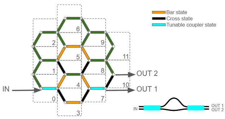
# Define a table of update instructions as (unit_cell, tunable_unit, voltage)update_table = [    (0, 0, v_tc),    (3, 1, v_cross),    (4, 0, v_bar),    (4, 2, v_cross),    (5, 0, v_bar),    (3, 0, v_bar),    (5, 1, v_bar),    (7, 0, v_cross),    (7, 2, v_bar),    (8, 0, v_cross),    (8, 2, v_bar),    (7, 1, v_tc),    (10, 0, v_cross),]
# Create the updates dictionary using the tableupdates = {    ("Unit Cell", uc, "Tunable Unit", tu, "Phase Shifter", 0): {        "model_updates": {"n_complex": index(v)}    }    for uc, tu, v in update_table}
# Compute the S-matrix of the full circuit using the programmed updatess_matrix = circuit.s_matrix(pf.C_0 / wavelengths, model_kwargs={"updates": updates})
# Plot transmission from input port P4 to output ports P16 and P20 in dBfig, ax = pf.plot_s_matrix(    s_matrix, input_ports=["P4"], output_ports=["P16", "P20"], y="dB")ax[0].set_xlim(1.57975, 1.58025)
Uploading task 'Mode-StripTE1550nmw500nm…'Uploading task 'Mode-StripTE1550nmw500nm…'Uploading task 'Mode-StripTE1550nmw500nm…'Uploading task 'Mode-StripTE1550nmw500nm…'Starting task 'Mode-StripTE1550nmw500nm': https://tidy3d.simulation.cloud/workbench?taskId=mo-91526e79-6c33-4412-9097-fae059748e3eStarting task 'Mode-StripTE1550nmw500nm': https://tidy3d.simulation.cloud/workbench?taskId=mo-b3fed9a2-ec83-4bcb-93b4-02341e4b8746Starting task 'Mode-StripTE1550nmw500nm': https://tidy3d.simulation.cloud/workbench?taskId=mo-57fd7eae-c859-4b14-9904-7fa0e8357cb6Starting task 'Mode-StripTE1550nmw500nm': https://tidy3d.simulation.cloud/workbench?taskId=mo-73152fe2-59a3-42c4-b383-11ba344f4be7Downloading data from 'Mode-StripTE1550nmw500nm'…Downloading data from 'Mode-StripTE1550nmw500nm'…Downloading data from 'Mode-StripTE1550nmw500nm'…Downloading data from 'Mode-StripTE1550nmw500nm'…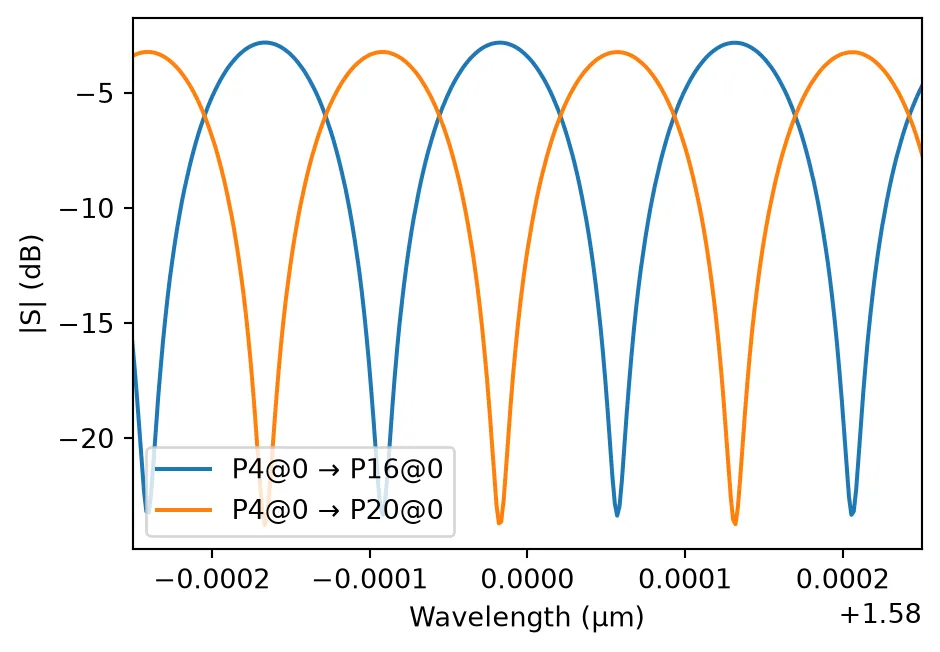
Sweeping the Tunable Coupler Voltage
To study the tunability of the unbalanced Mach-Zehnder Interferometer (MZI), we sweep the voltage applied to the two tunable couplers used in the configuration. These couplers were initially set to v_tc, and here we evaluate the system’s spectral response as we slightly detune this voltage to 0.9 × v_tc and 0.8 × v_tc.
We update the complex refractive index of the corresponding phase shifters for each voltage and recompute the circuit’s S-matrix. The resulting transmission spectra to the two output ports (P16 and P20) are plotted in dB scale to observe changes in the interference pattern, indicating the effect of voltage tuning on output power distribution.
# --- prepare your sweep parameters ---v_tc_values = [0.8 * v_tc, 0.9 * v_tc, v_tc]  # voltage sweep for tunable couplerscolors = ["C0", "C1", "C2"]  # matplotlib color codeslabels = [f"v_tc = {v:.2f}" for v in v_tc_values]  # labels for legend
# Specify the two tunable couplers whose voltage will be swepttc_keys = [    ("Unit Cell", 0, "Tunable Unit", 0, "Phase Shifter", 0),    ("Unit Cell", 7, "Tunable Unit", 1, "Phase Shifter", 0),]
# Create plot with two subplots: one for each output portfig, ax = plt.subplots(1, 2, figsize=(10, 4), tight_layout=True)
# Loop through the voltage values to compute and plot resultsfor v_tc, color, label in zip(v_tc_values, colors, labels):    # Copy the base updates and override the tunable coupler voltages    upd = {**updates}    for m in tc_keys:        upd[m] = {"model_updates": {"n_complex": index(v_tc)}}
    # Compute the S-matrix for the current voltage setting    sm = circuit.s_matrix(frequencies, model_kwargs={"updates": upd})
    # Extract S-parameters from input to each output port    out1 = sm[("P0@0", "P16@0")]  # output 1    out2 = sm[("P0@0", "P20@0")]  # output 2
    # Convert to dB scale    out1_db = 20 * np.log10(np.abs(out1))    out2_db = 20 * np.log10(np.abs(out2))
    # Plot transmission to both output ports    ax[0].plot(wavelengths, out1_db, color=color, label=label)    ax[1].plot(wavelengths, out2_db, color=color, label=label)
# Set axis labels and formatting for Output 1ax[0].set_xlim(1.57975, 1.58025)ax[0].set_xlabel("Wavelength (µm)")ax[0].set_ylabel("Output 1 (dB)")ax[0].legend()
# Set axis labels and formatting for Output 2ax[1].set_xlim(1.57975, 1.58025)ax[1].set_xlabel("Wavelength (µm)")ax[1].set_ylabel("Output 2 (dB)")ax[1].legend()
# Show the final plotplt.show()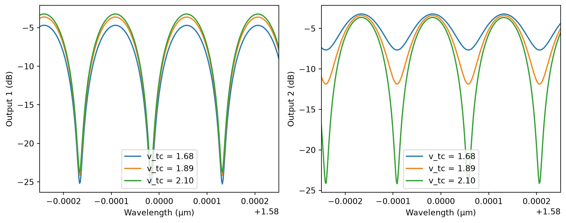
Ring Resonator
Section titled “Ring Resonator”We configure the programmable hexagonal photonic circuit to realize a ring resonator by programming a closed loop of tunable units as shown in the schematic. The loop is formed by setting specific units into bar or tunable coupler states to guide light around the ring.
The input light enters at port P12 and circulates through the ring, with output observed at ports P4 and P8. The transmission spectrum is plotted in dB scale to reveal resonant behavior within a narrow wavelength band centered at 1.58 µm.
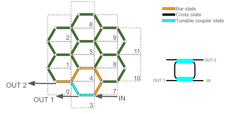
# Define a table of update instructions for the ring resonator configurationring_update_table = [    (0, 0, v_bar),    (3, 0, v_tc),    (3, 1, v_tc),    (4, 0, v_bar),    (4, 1, v_bar),    (7, 0, v_bar),    (7, 2, v_bar),]
# Create the updates dictionary using the tableupdates = {    ("Unit Cell", uc, "Tunable Unit", tu, "Phase Shifter", 0): {        "model_updates": {"n_complex": index(v)}    }    for uc, tu, v in ring_update_table}
# Compute the circuit S-matrix with the ring resonator configurations_matrix = circuit.s_matrix(pf.C_0 / wavelengths, model_kwargs={"updates": updates})
# Plot the transmission spectrum from input port P12 to output ports P4 and P8fig, ax = pf.plot_s_matrix(    s_matrix, input_ports=["P12"], output_ports=["P4", "P8"], y="dB")ax[0].set_xlim(1.57975, 1.58025)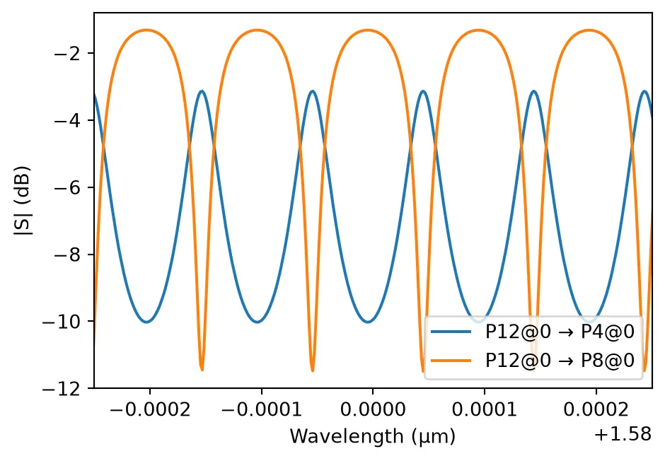
Tuning the Coupling Strength in the Ring Resonator
To examine how the resonance behavior of the ring resonator changes with different coupling strengths, we perform a voltage sweep on the two tunable couplers that control coupling into and out of the ring. By varying the voltage around the nominal tunable coupler setting v_tc, we effectively change the power coupling ratio between the bus waveguide and the resonator.
# --- prepare your sweep parameters ---v_tc_values = [1.35 * v_tc, 1.15 * v_tc, v_tc]colors = ["C0", "C1", "C2"]labels = [f"v_tc = {v:.2f}" for v in v_tc_values]
# pick out the two Phase Shifter keys that you want to vary with v_tctc_keys = [    ("Unit Cell", 3, "Tunable Unit", 0, "Phase Shifter", 0),    ("Unit Cell", 3, "Tunable Unit", 1, "Phase Shifter", 0),]
# name of the S-parameter you care about:port_pair = ()
fig, ax = plt.subplots(1, 2, figsize=(10, 4), tight_layout=True)
for v_tc, color, label in zip(v_tc_values, colors, labels):    # make a copy of your updates and override v_tc on the two keys    upd = {**updates}    for m in tc_keys:        upd[m] = {"model_updates": {"n_complex": index(v_tc)}}
    # compute new S-matrix    sm = circuit.s_matrix(frequencies, model_kwargs={"updates": upd})
    # extract the vector and convert to dB    out1 = sm[("P12@0", "P8@0")]  # complex values    out2 = sm[("P12@0", "P4@0")]  # complex values    out1_db = 20 * np.log10(np.abs(out1))  # to dB    out2_db = 20 * np.log10(np.abs(out2))  # to dB
    # plot    ax[0].plot(wavelengths, out1_db, color=color, label=label)    ax[1].plot(wavelengths, out2_db, color=color, label=label)
# formattingax[0].set_xlim(1.57975, 1.58025)ax[0].set_xlabel("Wavelength (µm)")ax[0].set_ylabel("Output 1 (dB)")ax[0].legend()ax[1].set_xlim(1.57975, 1.58025)ax[1].set_xlabel("Wavelength (µm)")ax[1].set_ylabel("Output 2 (dB)")ax[1].legend()plt.show()