Switch Array
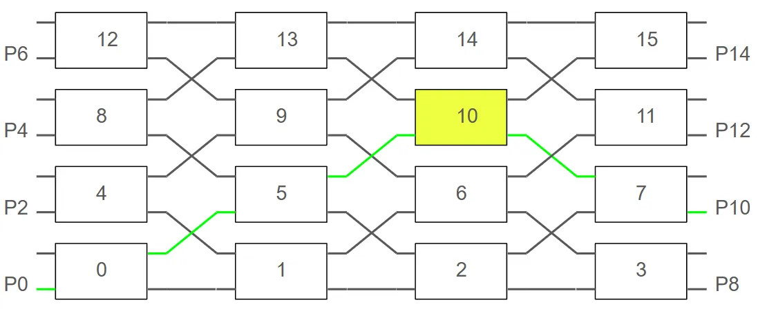
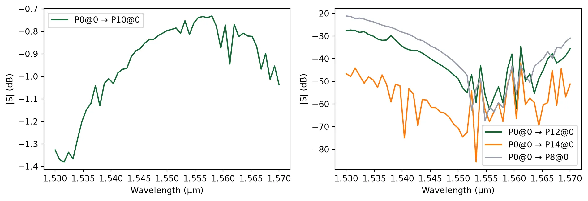
In this notebook, we create a switch array inspired by the work of Suzuki et al. [1], which demonstrated a 32×32 silicon photonic switch with ultra-low insertion loss and power-efficient operation. Their design utilizes a high-Δ silica planar lightwave circuit (PLC) platform to achieve compact and low-crosstalk routing. The switch architecture enables scalable integration of photonic components with precise routing of optical signals across multiple paths.
We implement a scalable version of such a switch using an array of unit cells, where each unit cell can be interconnected via parameterized routing. Our implementation mimics the concept of highly efficient and integrated photonic switching fabrics proposed in [1].
This architecture is particularly advantageous when using p-i-n junctions for fast switching. In such cases, carrier injection through the junction introduces additional loss, which can increase insertion loss, degrade uniformity, and cause crosstalk. However, in this architecture, only one Mach–Zehnder Interferometer is active per switching configuration, resulting in consistently low insertion loss and improved signal uniformity across the array [2].
References
- Suzuki, Keijiro, et al. “Low-insertion-loss and power-efficient 32×32 silicon photonics switch with extremely high-Δ silica PLC connector.” Journal of Lightwave Technology 2019 37 (1), 116-122, doi: 10.1109/JLT.2018.2867575.
- Konoike, Ryotaro, Keijiro Suzuki, and Kazuhiro Ikeda. “Path-independent insertion loss 8× 8 silicon photonics switch with nanosecond-order switching time.” Journal of Lightwave Technology 2023 41 (3), 865-870, doi: 10.1364/JLT.41.000865
- Y. Ma et al., “Ultralow loss single layer submicron silicon waveguide crossing for SOI optical interconnect,” Opt Express, 2023 21 (24), 29374–29382, doi: 10.1364/OE.21.029374
import matplotlib.pyplot as pltimport numpy as npimport photonforge as pfimport siepic_forge as siepic_pdkimport tidy3d as tdfrom photonforge.live_viewer import LiveViewer
viewer = LiveViewer()
LiveViewer started at http://127.0.0.1:43055. Call its 'stop()' method to free the port.We start by setting up the simulation environment using the SiEPIC OpenEBL PDK platform. This includes defining waveguide parameters, default simulation settings, and wavelength ranges. The technology is configured to use Tidy3D for simulating components such as bends and S-bends.
To focus the simulation, we define a narrow wavelength sweep around 1.55 µm—representing the telecom C-band—and convert this wavelength range to corresponding optical frequencies for use in frequency-domain simulations.
bend_radius = 10  # default bend radius in micronswg_width = 0.43  # waveguide width in micronswidth_nm = int(wg_width * 1e3)
# Load SiEPIC OpenEBL technology PDKtech = siepic_pdk.ebeam()
# Set the default technology to SiEPIC OpenEBLpf.config.default_technology = tech
# Set Tidy3D logging level to suppress non-critical messagestd.config.logging.level = "ERROR"
# Configure default parameters for photonic componentspf.config.default_kwargs = {    "bend": {"model": pf.Tidy3DModel()},    "s_bend": {"model": pf.Tidy3DModel()},    "radius": bend_radius,  # default bend radius    "euler_fraction": 0.5,  # Euler bend fraction}
# Define wavelength range for the simulationwavelengths = np.linspace(1.53, 1.57, 51)
lambda_0 = 1.55  # central wavelength in microns
# Convert wavelengths to frequencies (Hz)frequencies = pf.C_0 / wavelengths
Additionally, we configure the port specification to use a 430 nm–wide waveguide—matching the design in [1]—and integrate this port into the technology.
# copy & tweak the existing 500 nm TE portport_spec = tech.ports["TE_1550_500"].copy()port_spec.path_profiles = [(wg_width, 0.0, (1, 0))]
# build your new port name & description from wg_widthport_name = f"TE_1550_{width_nm}"port_spec.description = f"Strip TE 1550 nm, w={width_nm} nm"
# register ittech.add_port(port_name, port_spec)Layers
| Name | Layer | Description | Color | Pattern | Device marker | Conductive | Min. width (μm) | Min. spacing (μm) |
|---|---|---|---|---|---|---|---|---|
| Si | (1, 0) | SiEPIC - Waveguide | #ff80a818 | \\ | ||||
| PinRec | (1, 10) | SiEPIC | #ff80a818 | xx | ||||
| PinRecM | (1, 11) | SiEPIC | #80000018 | + | ||||
| Si Slab | (2, 0) | Dedicated Run Layers - Device…… Layer Partial Etch | #c080ff18 | / | ||||
| Direct Metal | (5, 0) | Dedicated Run Layers | #80a8ff18 | || | ||||
| Oxide open to BOX | (6, 0) | Dedicated Run Layers | #ff000018 | - | ||||
| Text | (10, 0) | Text-Not Fabricated | #00000018 | hollow | ||||
| M1_heater | (11, 0) | TiW Heater | #0000ff18 | \\ | ||||
| M2_router | (12, 0) | TiW/Au Routing Bilayer | #ffbf0018 | // | ||||
| M_Open | (13, 0) | Bond Pad Open | #80005718 | \\ | ||||
| Si n | (20, 0) | Dedicated Run Layers | #afff8018 | - | ||||
| Si p | (21, 0) | Dedicated Run Layers | #ffd9df18 | = | ||||
| Si n+ | (22, 0) | Dedicated Run Layers | #ff800018 | x | ||||
| Si p+ | (23, 0) | Dedicated Run Layers | #ddff0018 | xx | ||||
| Si n++ | (24, 0) | Dedicated Run Layers | #00ffff18 | + | ||||
| Si p++ | (25, 0) | Dedicated Run Layers | #00800018 | ++ | ||||
| ANT Reserved | (31, 0) | SiEPIC/ANT Reserved | #9580ff18 | / | ||||
| ANT Reserved 1 | (33, 0) | ANT Reserved | #9580ff18 | / | ||||
| Via to silicon | (40, 0) | Dedicated Run Layers | #0000ff18 | . | ||||
| DevRec | (68, 0) | SiEPIC | #00800018 | . | ||||
| FbrTgt | (81, 0) | SiEPIC/Dedicated Run Layers | #80808018 | ++ | ||||
| ANT Reserved 2 | (102, 0) | ANT Reserved | #9580ff18 | / | ||||
| ANT Reserved 3 | (110, 0) | ANT Reserved | #9580ff18 | / | ||||
| Custom Dicing | (189, 0) | #00000018 | hollow | |||||
| SEM Imaging | (200, 0) | #ff000018 | x | |||||
| Deep Trench | (201, 0) | #00ff0018 | . | |||||
| Deep Trench Handling Exclusion | (202, 0) | #00760018 | : | |||||
| Thermal Isolation Trenches | (203, 0) | #00800018 | \ | |||||
| Laser Integration Shelf | (205, 0) | Dedicated Run Layers | #69ff0518 | xx | ||||
| Floor Plan-Not Fabricated | (290, 0) | #c080ff18 | hollow | |||||
Error: device layer width is…… less than design rule | (301, 0) | DRC Errors | #80005718 | = | ||||
Error: device layer spacing is…… less than design rule | (301, 1) | DRC Errors | #80005718 | - | ||||
Warning: polygons/paths on…… PinRec layer (1/10) will NOT be fabricated | (301, 2) | DRC Errors | #80005718 | || | ||||
Error: direct metal width is…… less than 5 microns | (305, 0) | DRC Errors | #80808018 | ++ | ||||
Error: direct metal spacing is…… less than 10 microns | (305, 1) | DRC Errors | #80808018 | + | ||||
Error: TiW width is less than 3…… microns | (311, 0) | DRC Errors | #ffa08018 | // | ||||
Error: TiW spacing is less than…… 3 microns | (311, 1) | DRC Errors | #ffa08018 | / | ||||
Error: Al width is less than…… design rule | (312, 0) | DRC Errors | #00ffff18 | | | ||||
Error: Al spacing is less than…… design rule | (312, 1) | DRC Errors | #00ffff18 | // | ||||
Error: Spacing between TiW and…… Al is less than 5 microns | (312, 3) | DRC Errors | #00ffff18 | \\ | ||||
Error: Oxide window width is…… less than 10 microns | (313, 0) | DRC Errors | #01ff6b18 | || | ||||
Error: Oxide window spacing is…… less than 10 microns | (313, 1) | DRC Errors | #01ff6b18 | | | ||||
Error: Oxide window is not…… placed over Al | (313, 2) | DRC Errors | #01ff6b18 | // | ||||
| Standard Design Area | (350, 0) | DRC Errors | #ddff0018 | \ | ||||
Error: Features outside design…… area. Verify design size and centering. | (350, 1) | DRC Errors | #ddff0018 | : | ||||
Error: Dicing lane width is…… less than 100 microns | (389, 0) | DRC Errors | #ff00ff18 | ++ | ||||
Error: Spacing between dicing…… lane and devices is less than 50 microns | (389, 1) | DRC Errors | #ff00ff18 | + | ||||
Error: SEM width is less than…… 500 nm | (400, 0) | DRC Errors | #ff9d9d18 | x | ||||
| Deep Trench Design Area | (401, 0) | DRC Errors | #80a8ff18 | xx | ||||
Error: Metal, SEM, or handling…… region overlap with deep trenches. Verify design centering | (401, 1) | DRC Errors | #80a8ff18 | x | ||||
Warning: Silicon features…… outside deep trench design area. Verify accuracy before submission | (401, 2) | DRC Errors | #80a8ff18 | = | ||||
Error: Spacing between metal…… and deep trench is less than 30 microns | (401, 3) | DRC Errors | #80a8ff18 | - | ||||
Error: Deep trench width is…… less than 260 microns | (401, 4) | DRC Errors | #80a8ff18 | || | ||||
Error: Deep trench handling…… area missing. Please add handling area of size shown by polygons | (402, 0) | DRC Errors | #ff000018 | + | ||||
Error: Features inside deep…… trench handling area | (402, 1) | DRC Errors | #ff000018 | xx | ||||
Error: Thermal isolation width…… is less than design rule | (403, 0) | DRC Errors | #50008018 | ++ | ||||
Error: Thermal isolation…… spacing is less than design rule | (403, 1) | DRC Errors | #50008018 | + | ||||
Error: Spacing between thermal…… isolation and metal is less than design rule | (403, 2) | DRC Errors | #50008018 | xx | ||||
Error: Thermal isolation and…… device layer overlap, or spacing is less than design rule | (403, 3) | DRC Errors | #50008018 | x | ||||
Dream Photonics Black Box-Not…… Fabricated | (998, 0) | #00000018 | hollow | |||||
| Errors | (999, 0) | SiEPIC | #0000ff18 | || |
Extrusion specs
| # | Mask | Limits (μm) | Sidewall (°) | Opt. Medium | Elec. Medium |
|---|---|---|---|---|---|
| 0 | () | -inf, 0 | 0 | cSi_Li1993_293K | Si |
| 1 | () | -2, 2.5 | 0 | SiO2_Palik_LowLoss | SiO2 |
| 2 | 'M1_heater'**0.3 | 2.2, 2.7 | 0 | SiO2_Palik_LowLoss | SiO2 |
| 3 | 'M2_router'**0.3 | 2.2, 3.3 | 0 | SiO2_Palik_LowLoss | SiO2 |
| 4 | 'M1_heater' | 2.2, 2.4 | 0 | W_Werner2009 | LossyMetalMedium……(frequency_range=(100000000.0, 200000000000.0), conductivity=1.6, fit_param={'max_num_poles': 16}) |
| 5 | 'M2_router' | 2.4, 3 | 0 | Au_Olmon2012evaporated | LossyMetalMedium……(frequency_range=(100000000.0, 200000000000.0), conductivity=17.0, fit_param={'max_num_poles': 16}) |
| 6 | 'M_Open' | 3, 3.3 | 0 | Medium() | Medium() |
| 7 | 'Oxide open to BOX' | 0, inf | 0 | Medium() | Medium() |
| 8 | 'Si' | 0, 0.22 | 0 | cSi_Li1993_293K | Si |
| 9 | 'Si Slab' | 0, 0.09 | 0 | cSi_Li1993_293K | Si |
| 10 | 'Deep Trench' + 'Thermal…… Isolation Trenches' | -inf, inf | 0 | Medium() | Medium() |
Ports
| Name | Classification | Description | Width (μm) | Limits (μm) | Radius (μm) | Modes | Target n_eff | Path profiles (μm) |
|---|---|---|---|---|---|---|---|---|
| MM_TE_1550_2000 | optical | Multimode Strip TE 1550 nm,…… w=2000 nm | 6 | -2, 2.22 | 0 | 10 | 3.5 | 'Si': 2 |
| MM_TE_1550_3000 | optical | Multimode Strip TE 1550 nm,…… w=3000 nm | 6 | -2, 2.22 | 0 | 15 | 3.5 | 'Si': 3 |
| Rib_TE_1310_350 | optical | Rib (90 nm slab) TE 1310 nm,…… w=350 nm | 2.35 | -0.6, 0.82 | 0 | 1 | 3.5 | 'Si': 0.35, 'Si Slab': 3 |
| Rib_TE_1550_500 | optical | Rib (90 nm slab) TE 1550 nm,…… w=500 nm | 2.5 | -0.6, 0.82 | 0 | 1 | 3.5 | 'Si': 0.5, 'Si Slab': 3 |
| Slot_TE_1550_500 | optical | Slot TE 1550 nm, w=500 nm,…… gap=100nm | 3 | -1, 1.22 | 0 | 1 | 3.5 | 'Si': 0.2 (-0.15), 'Si': 0.2…… (+0.15) |
| TE-TM_1550_450 | optical | Strip TE-TM 1550, w=450 nm | 2.2 | -1, 1.22 | 0 | 2 | 3.5 | 'Si': 0.45 |
| TE_1310_350 | optical | Strip TE 1310 nm, w=350 nm | 1.5 | -0.6, 0.82 | 0 | 1 | 3.5 | 'Si': 0.35 |
| TE_1310_410 | optical | Strip TE 1310 nm, w=410 nm | 1.5 | -0.6, 0.82 | 0 | 1 | 3.5 | 'Si': 0.41 |
| TE_1550_430 | optical | Strip TE 1550 nm, w=430 nm | 1.5 | -0.6, 0.82 | 0 | 1 | 3.5 | 'Si': 0.43 |
| TE_1550_500 | optical | Strip TE 1550 nm, w=500 nm | 1.5 | -0.6, 0.82 | 0 | 1 | 3.5 | 'Si': 0.5 |
| TM_1310_350 | optical | Strip TM 1310 nm, w=350 nm | 1.5 | -0.6, 0.82 | 0 | 1 + 1 (TM) | 3.5 | 'Si': 0.35 |
| TM_1550_500 | optical | Strip TM 1550 nm, w=500 nm | 1.5 | -0.6, 0.82 | 0 | 1 + 1 (TM) | 3.5 | 'Si': 0.5 |
| eskid_TE_1550 | optical | eskid TE 1550 | 2 | -0.7, 0.92 | 0 | 1 | 3.5 | 'Si': 0.35, 'Si': 0.06…… (+0.265), 'Si': 0.06 (-0.265), 'Si': 0.06 (+0.385), 'Si': 0.06 (-0.385), 'Si': 0.06 (+0.505), 'Si': 0.06 (-0.505), 'Si': 0.06 (+0.625), 'Si': 0.06 (-0.625) |
Background medium
- Optical: Medium()
- Electrical: Medium()
We examine the port’s field profile to ensure it decays sufficiently at its boundaries; otherwise, we would adjust the port’s width and limits. In this case, the field has already decayed adequately.
mode_solver = pf.port_modes(port_spec, [pf.C_0 / lambda_0])mode_solver.plot_field("S", mode_index=0, scale="dB", vmin=-20, robust=False)Uploading task 'Mode-ModeSolver…'Starting task 'Mode-ModeSolver': https://tidy3d.simulation.cloud/workbench?taskId=mo-334decdc-be79-44e2-8178-12dd7471af94Downloading data from 'Mode-ModeSolver'…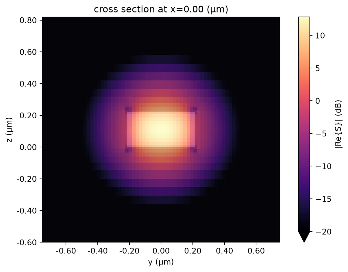
Angled Adiabatic Waveguide Crossing
Section titled “Angled Adiabatic Waveguide Crossing”We define a 4-arm angled adiabatic waveguide crossing with smooth cubic taper profiles, inspired by the device presented in [3]. This structure has been designed to minimize insertion loss and crosstalk by employing gradually varying widths along the propagation direction. The crossing is symmetrically constructed using four identical arms created through geometric operations.
The crossing incorporates adiabatic tapers formed via cubic spline interpolation, which ensures smooth transitions between waveguide widths. The component is constructed in compliance with symmetry conditions and is modeled using Tidy3D with specified port symmetries for reducing simulation costs.
from scipy.interpolate import make_interp_spline
default_widths = (    0.5,    0.6,    0.95,    1.32,    1.44,    1.46,    1.466,    1.52,    1.58,    1.62,    1.76,    2.15,    0.5,)
@pf.parametric_component(name_prefix="CROSSING")def angled_adiabatic_crossing(    *,    port_spec="TE_1550_500",    arm_length=4.5,    widths=default_widths,    radius=bend_radius,):    """    Create a 4-arm adiabatic crossing with smooth cubic taper profiles.
    Parameters:        port_spec (str or PortSpec): Input/output port specification name or object.        arm_length (float): Length of the main arm (µm).        widths (Sequence[float]): Target waveguide widths (µm) along each arm.        radius (float): Radius of the 45-deg arcs (µm).
    Returns:        A crossing component.    """    if isinstance(port_spec, str):        port_spec = pf.config.default_technology.ports[port_spec]
    wg_width, _ = port_spec.path_profile_for("Si")  # extract initial waveguide width
    # Number of points used to discretize the cubic spline profile.    num_points = int(arm_length / pf.config.tolerance)
    # Calculate port locations based on input dimensions (projected to the 45° axes)    projected_arm_length = arm_length * 2**-0.5    arc_y = radius * 2**-0.5    arc_x = radius - arc_y    # Snap port coordinates to the grid to avoid gaps/overlaps    xp = pf.snap_to_grid(projected_arm_length + arc_x)    yp = pf.snap_to_grid(projected_arm_length + arc_y)
    # Create cubic spline interpolation for widths    coords = np.linspace(0, projected_arm_length, len(widths))    # Reverse widths, because we're starting from 0 at the center of the cross    spline = make_interp_spline(coords, widths[::-1], k=3)
    # Pre-compute widths and positions from the interpolation    coords = np.linspace(projected_arm_length, 0, num_points)    widths = spline(coords)
    arm1 = pf.Path((xp, yp), wg_width)    arm1.arc(        0,        -45,        radius,        width=(widths[0], "smooth"),        endpoint=(projected_arm_length, projected_arm_length),    )    for x, w in zip(coords[1:], widths[1:]):        arm1.segment((x, x), w)
    arm2 = arm1.copy().mirror()    arm3 = arm1.copy().rotate(180)    arm4 = arm2.copy().rotate(180)
    c = pf.Component()    c.add("Si", *pf.boolean([arm1, arm2], [arm3, arm4], "+"))
    # Add ports    c.add_port(c.detect_ports([port_spec]))    assert len(c.ports) == 4, "Port detection failed: expected exactly 4 ports."
    # Add Tidy3D simulation model with symmetry conditions    c.add_model(        pf.Tidy3DModel(            port_symmetries=[                ("P1", "P0", "P3", "P2"),  # symmetry about x-axis                ("P2", "P3", "P0", "P1"),  # symmetry about y-axis                ("P3", "P2", "P1", "P0"),  # inversion symmetry            ],        ),        "Tidy3DModel",    )    return c
crossing = angled_adiabatic_crossing(port_spec=port_spec)viewer(crossing)
To evaluate the optical performance of the angled adiabatic crossing, we compute its scattering matrix (S-matrix) over the defined wavelength range. The S-matrix characterizes the power transmission and reflection between each pair of ports. We then visualize the resulting S-matrix to inspect insertion loss and crosstalk across the device.
# Compute the scattering matrix of the crossing over the frequency ranges_matrix_crossing = crossing.s_matrix(frequencies)
# Plot the magnitude of the S-matrix to evaluate transmission and crosstalk_ = pf.plot_s_matrix(s_matrix_crossing)
Uploading task 'P0@0…'Starting task 'P0@0': https://tidy3d.simulation.cloud/workbench?taskId=fdve-66bfdb20-0b45-4b90-9807-2ded26e75872Downloading data from 'P0@0'…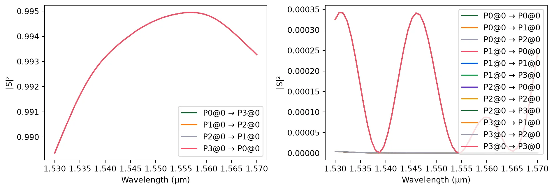
Directional Coupler
Section titled “Directional Coupler”We define a dual-ring directional directional coupler to be used in the switch array. The design includes two curved waveguides with a specified coupling distance and coupling length. The radius and Euler bend fraction are set to ensure adiabatic transitions. To facilitate efficient simulation with Tidy3D, we explicitly define the port symmetries, ensuring accurate modeling of the device behavior.
# Define a dual-ring directional coupler with specified geometry and waveguide spacingdc_coupler = pf.parametric.dual_ring_coupler(    port_spec=port_spec,  # use predefined port specification    coupling_distance=0.75,  # gap between the coupled waveguides (µm)    radius=5,  # bend radius (µm)    euler_fraction=0.5,  # fraction of Euler bend    coupling_length=20.8,  # coupling region length (µm)    model=pf.Tidy3DModel(),)
# Define symmetries for accurate simulation with Tidy3Ddc_coupler.models["Tidy3D"].port_symmetries = [    ("P1", "P0", "P3", "P2"),  # x-axis reflection    ("P2", "P3", "P0", "P1"),  # y-axis reflection    ("P3", "P2", "P1", "P0"),  # inversion symmetry]
dc_length, dc_width = dc_coupler.size()
viewer(dc_coupler)  # Display the coupler
We simulate the dual-ring coupler to extract its S-matrix across the defined frequency range.
# Compute the S-matrix of the dual-ring coupler over the specified frequenciess_matrix_dc = dc_coupler.s_matrix(frequencies)
# Plot the S-matrix to visualize power transmission and coupling behavior_ = pf.plot_s_matrix(s_matrix_dc)
Uploading task 'P0@0…'Starting task 'P0@0': https://tidy3d.simulation.cloud/workbench?taskId=fdve-8bb07609-c229-45d4-afaf-143d4c47987fDownloading data from 'P0@0'…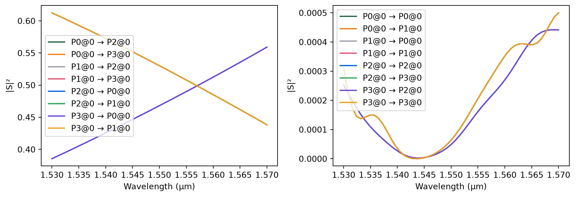
Thermal Phase Shifter
Section titled “Thermal Phase Shifter”We model a straight waveguide to serve as a thermal phase shifter. To account for propagation loss, we compute the imaginary part of the refractive index from a specified loss value in dB/cm. Using mode solving, we extract the complex effective index across the wavelength range.
We then define a function that maps applied voltage to a change in the real part of the refractive index, simulating the thermo-optic effect. This function enables modeling phase modulation based on input voltage. Finally, we assign the zero-voltage thermal model as the default waveguide model in the phase shifter component.
wg_length = 70  # length of the straight waveguide in micronsalpha = 3  # propagation loss in dB/cm
# Calculate imaginary part of refractive index from losskappa = (alpha * wavelengths * 1e-4 * np.log(10)) / (40 * np.pi)
# Solve for waveguide modes to obtain complex effective indexmode_solver = pf.port_modes(port=port_spec, frequencies=pf.C_0 / wavelengths)n_complex = mode_solver.data.n_complex.values.T + 1j * kappa  # include loss in index
# Create straight waveguide to model thermal phase shifterphase_shifter = pf.parametric.straight(    port_spec=port_spec, length=wg_length, name="Phase Shifter")wg = pf.parametric.straight(port_spec=port_spec, length=wg_length, name="wg")wg_model = pf.WaveguideModel(n_complex=n_complex)wg.add_model(wg_model)  # assign loss model to auxiliary waveguide
# Define voltage-dependent refractive index model for thermal tuningdef index(voltage, resistance=0.9, coefficient=1e-3):    """    Calculate complex refractive index as a function of applied voltage.
    Parameters:        voltage (float): Applied voltage (V).        resistance (float): Heater resistance (Ω).        coefficient (float): Proportionality constant.
    Returns:        np.ndarray: Complex refractive index array.    """    dn = coefficient * voltage**2 / resistance  # thermo-optic phase shift    return n_complex + dn
# Set the default waveguide model at 0 V as the initial thermal modelthermal_model = pf.WaveguideModel(n_complex=index(0))
# Add thermal model to phase shifter component_ = phase_shifter.add_model(thermal_model, "Waveguide")
Uploading task 'Mode-ModeSolver…'Starting task 'Mode-ModeSolver': https://tidy3d.simulation.cloud/workbench?taskId=mo-1172bf26-4286-4ae6-8cc5-30f0bb632802Downloading data from 'Mode-ModeSolver'…Tunable Mach–Zehnder Interferometer (MZI)
Section titled “Tunable Mach–Zehnder Interferometer (MZI)”We construct a tunable Mach–Zehnder Interferometer using a netlist-based approach. The MZI consists of two directional couplers and two thermal phase shifters placed in each interferometer arm. Routing is done automatically between connected ports, ensuring proper alignment and spacing.
By configuring the thermal phase shifters with voltage-dependent refractive index models, this MZI design enables dynamic phase control and interference tuning, which are essential for applications like modulation and switching in photonic circuits.
netlist_mzi = {    "name": "Tunable MZI",  # name of the component    "instances": {        "dc0": dc_coupler,  # first directional coupler        "ps0": {            "component": phase_shifter,            "origin": (dc_length + bend_radius, -wg_length / 2 - dc_width),  # lower arm        },        "ps1": {            "component": phase_shifter,            "origin": (dc_length + bend_radius, wg_length / 2),  # upper arm        },        "dc1": {            "component": dc_coupler,            "origin": (                2 * dc_length + 2 * bend_radius + wg_length,                0,            ),  # second coupler        },    },    # Define waveguide routes between instances    "routes": [        (("dc0", "P2"), ("ps0", "P0"), pf.parametric.route),        (("dc0", "P3"), ("ps1", "P0"), pf.parametric.route),        (("dc1", "P1"), ("ps1", "P1"), pf.parametric.route),        (("dc1", "P0"), ("ps0", "P1"), pf.parametric.route),    ],    # Expose external ports    "ports": [("dc0", "P0"), ("dc0", "P1"), ("dc1", "P2"), ("dc1", "P3")],    # Assign simulation model for the full circuit    "models": [(pf.CircuitModel(), "Circuit")],}
# Create the MZI component from the defined netlistmzi = pf.component_from_netlist(netlist_mzi)
# Visualize the MZIviewer(mzi);fill:%23221f20;font-weight:bold;font-size:3.994800px;}.terminal{fill:none;stroke:%23805080;stroke-width:0.499350;}.dashed{stroke-dasharray:2.496750,1.498050;}.port{fill:none;stroke:%23805080;stroke-width:0.998700;}.virtual-connection{fill:none;stroke:%23907090;stroke-width:0.749025;}.layer_31_0{stroke:%238c78ef;fill:url(%23pat-layer_31_0);fill-opacity:0.492;}.label_31_0{fill:%238c78ef;}.layer_33_0{stroke:%238c78ef;fill:url(%23pat-layer_33_0);fill-opacity:0.492;}.label_33_0{fill:%238c78ef;}.layer_102_0{stroke:%238c78ef;fill:url(%23pat-layer_102_0);fill-opacity:0.492;}.label_102_0{fill:%238c78ef;}.layer_110_0{stroke:%238c78ef;fill:url(%23pat-layer_110_0);fill-opacity:0.492;}.label_110_0{fill:%238c78ef;}.layer_189_0{stroke:%23000000;fill:none;}.label_189_0{fill:%23000000;}.layer_201_0{stroke:%2300ee00;fill:url(%23pat-layer_201_0);fill-opacity:0.492;}.label_201_0{fill:%2300ee00;}.layer_401_0{stroke:%236a8ad2;fill:url(%23pat-layer_401_0);fill-opacity:0.492;}.label_401_0{fill:%236a8ad2;}.layer_202_0{stroke:%23007600;fill:url(%23pat-layer_202_0);fill-opacity:0.492;}.label_202_0{fill:%23007600;}.layer_68_0{stroke:%23008000;fill:url(%23pat-layer_68_0);fill-opacity:0.492;}.label_68_0{fill:%23008000;}.layer_5_0{stroke:%236a8ad2;fill:url(%23pat-layer_5_0);fill-opacity:0.492;}.label_5_0{fill:%236a8ad2;}.layer_998_0{stroke:%23000000;fill:none;}.label_998_0{fill:%23000000;}.layer_312_1{stroke:%2300b8b8;fill:url(%23pat-layer_312_1);fill-opacity:0.492;}.label_312_1{fill:%2300b8b8;}.layer_312_0{stroke:%2300b8b8;fill:url(%23pat-layer_312_0);fill-opacity:0.492;}.label_312_0{fill:%2300b8b8;}.layer_402_0{stroke:%23ff0000;fill:url(%23pat-layer_402_0);fill-opacity:0.492;}.label_402_0{fill:%23ff0000;}.layer_401_4{stroke:%236a8ad2;fill:url(%23pat-layer_401_4);fill-opacity:0.492;}.label_401_4{fill:%236a8ad2;}.layer_389_0{stroke:%23ff00ff;fill:url(%23pat-layer_389_0);fill-opacity:0.492;}.label_389_0{fill:%23ff00ff;}.layer_402_1{stroke:%23ff0000;fill:url(%23pat-layer_402_1);fill-opacity:0.492;}.label_402_1{fill:%23ff0000;}.layer_350_1{stroke:%23697a00;fill:url(%23pat-layer_350_1);fill-opacity:0.492;}.label_350_1{fill:%23697a00;}.layer_401_1{stroke:%236a8ad2;fill:url(%23pat-layer_401_1);fill-opacity:0.492;}.label_401_1{fill:%236a8ad2;}.layer_313_2{stroke:%2301d95b;fill:url(%23pat-layer_313_2);fill-opacity:0.492;}.label_313_2{fill:%2301d95b;}.layer_313_1{stroke:%2301d95b;fill:url(%23pat-layer_313_1);fill-opacity:0.492;}.label_313_1{fill:%2301d95b;}.layer_313_0{stroke:%2301d95b;fill:url(%23pat-layer_313_0);fill-opacity:0.492;}.label_313_0{fill:%2301d95b;}.layer_400_0{stroke:%23a96868;fill:url(%23pat-layer_400_0);fill-opacity:0.492;}.label_400_0{fill:%23a96868;}.layer_312_3{stroke:%2300b8b8;fill:url(%23pat-layer_312_3);fill-opacity:0.492;}.label_312_3{fill:%2300b8b8;}.layer_389_1{stroke:%23ff00ff;fill:url(%23pat-layer_389_1);fill-opacity:0.492;}.label_389_1{fill:%23ff00ff;}.layer_401_3{stroke:%236a8ad2;fill:url(%23pat-layer_401_3);fill-opacity:0.492;}.label_401_3{fill:%236a8ad2;}.layer_403_2{stroke:%23500080;fill:url(%23pat-layer_403_2);fill-opacity:0.492;}.label_403_2{fill:%23500080;}.layer_403_3{stroke:%23500080;fill:url(%23pat-layer_403_3);fill-opacity:0.492;}.label_403_3{fill:%23500080;}.layer_403_1{stroke:%23500080;fill:url(%23pat-layer_403_1);fill-opacity:0.492;}.label_403_1{fill:%23500080;}.layer_403_0{stroke:%23500080;fill:url(%23pat-layer_403_0);fill-opacity:0.492;}.label_403_0{fill:%23500080;}.layer_311_1{stroke:%23ac6c56;fill:url(%23pat-layer_311_1);fill-opacity:0.492;}.label_311_1{fill:%23ac6c56;}.layer_311_0{stroke:%23ac6c56;fill:url(%23pat-layer_311_0);fill-opacity:0.492;}.label_311_0{fill:%23ac6c56;}.layer_301_1{stroke:%23800057;fill:url(%23pat-layer_301_1);fill-opacity:0.492;}.label_301_1{fill:%23800057;}.layer_301_0{stroke:%23800057;fill:url(%23pat-layer_301_0);fill-opacity:0.492;}.label_301_0{fill:%23800057;}.layer_305_1{stroke:%23808080;fill:url(%23pat-layer_305_1);fill-opacity:0.492;}.label_305_1{fill:%23808080;}.layer_305_0{stroke:%23808080;fill:url(%23pat-layer_305_0);fill-opacity:0.492;}.label_305_0{fill:%23808080;}.layer_999_0{stroke:%230000ff;fill:url(%23pat-layer_999_0);fill-opacity:0.492;}.label_999_0{fill:%230000ff;}.layer_81_0{stroke:%23808080;fill:url(%23pat-layer_81_0);fill-opacity:0.492;}.label_81_0{fill:%23808080;}.layer_290_0{stroke:%23a46eda;fill:none;}.label_290_0{fill:%23a46eda;}.layer_205_0{stroke:%2349b203;fill:url(%23pat-layer_205_0);fill-opacity:0.492;}.label_205_0{fill:%2349b203;}.layer_11_0{stroke:%230000ff;fill:url(%23pat-layer_11_0);fill-opacity:0.492;}.label_11_0{fill:%230000ff;}.layer_12_0{stroke:%23a57b00;fill:url(%23pat-layer_12_0);fill-opacity:0.492;}.label_12_0{fill:%23a57b00;}.layer_13_0{stroke:%23800057;fill:url(%23pat-layer_13_0);fill-opacity:0.492;}.label_13_0{fill:%23800057;}.layer_6_0{stroke:%23ff0000;fill:url(%23pat-layer_6_0);fill-opacity:0.492;}.label_6_0{fill:%23ff0000;}.layer_1_10{stroke:%23c96585;fill:url(%23pat-layer_1_10);fill-opacity:0.492;}.label_1_10{fill:%23c96585;}.layer_1_11{stroke:%23800000;fill:url(%23pat-layer_1_11);fill-opacity:0.492;}.label_1_11{fill:%23800000;}.layer_200_0{stroke:%23ff0000;fill:url(%23pat-layer_200_0);fill-opacity:0.492;}.label_200_0{fill:%23ff0000;}.layer_1_0{stroke:%23c96585;fill:url(%23pat-layer_1_0);fill-opacity:0.492;}.label_1_0{fill:%23c96585;}.layer_2_0{stroke:%23a46eda;fill:url(%23pat-layer_2_0);fill-opacity:0.492;}.label_2_0{fill:%23a46eda;}.layer_20_0{stroke:%2353793d;fill:url(%23pat-layer_20_0);fill-opacity:0.492;}.label_20_0{fill:%2353793d;}.layer_22_0{stroke:%23ec7600;fill:url(%23pat-layer_22_0);fill-opacity:0.492;}.label_22_0{fill:%23ec7600;}.layer_24_0{stroke:%2300b8b8;fill:url(%23pat-layer_24_0);fill-opacity:0.492;}.label_24_0{fill:%2300b8b8;}.layer_21_0{stroke:%23736264;fill:url(%23pat-layer_21_0);fill-opacity:0.492;}.label_21_0{fill:%23736264;}.layer_23_0{stroke:%23697a00;fill:url(%23pat-layer_23_0);fill-opacity:0.492;}.label_23_0{fill:%23697a00;}.layer_25_0{stroke:%23008000;fill:url(%23pat-layer_25_0);fill-opacity:0.492;}.label_25_0{fill:%23008000;}.layer_350_0{stroke:%23697a00;fill:url(%23pat-layer_350_0);fill-opacity:0.492;}.label_350_0{fill:%23697a00;}.layer_10_0{stroke:%23000000;fill:none;}.label_10_0{fill:%23000000;}.layer_203_0{stroke:%23008000;fill:url(%23pat-layer_203_0);fill-opacity:0.492;}.label_203_0{fill:%23008000;}.layer_40_0{stroke:%230000ff;fill:url(%23pat-layer_40_0);fill-opacity:0.492;}.label_40_0{fill:%230000ff;}.layer_401_2{stroke:%236a8ad2;fill:url(%23pat-layer_401_2);fill-opacity:0.492;}.label_401_2{fill:%236a8ad2;}.layer_301_2{stroke:%23800057;fill:url(%23pat-layer_301_2);fill-opacity:0.492;}.label_301_2{fill:%23800057;}</style><defs><path id=%22port-symbol%22 class=%22port%22 d=%22M 0,-1.997400 L 2.996100,0 0,1.997400%22 /><path id=%22ref-port-symbol%22 class=%22port%22 style=%22stroke-opacity:0.33;%22 d=%22M 0,-1.498050 C 1.997400,-1.498050 1.997400,1.498050 0,1.498050%22 /><circle id=%22port-bend-symbol%22 style=%22stroke-width:0;stroke:none;fill:%23805080;fill-opacity:1;%22 cx=%220%22 cy=%220%22 r=%220.898830%22 /><circle id=%22connection-symbol%22 style=%22stroke-width:0;stroke:none;fill:%23907090;fill-opacity:1;%22 cx=%220%22 cy=%220%22 r=%221.048635%22 /><pattern id=%22pat-layer_31_0%22 patternUnits=%22userSpaceOnUse%22 width=%222.496750%22 height=%222.496750%22 patternTransform=%22translate(1.909279,2.365342)%22><line x1=%220%22 y1=%220%22 x2=%222.496750%22 y2=%222.496750%22 style=%22stroke:%238c78ef;stroke-width:0.249675%22 /><line x1=%22-1.248375%22 y1=%221.248375%22 x2=%221.248375%22 y2=%223.745125%22 style=%22stroke:%238c78ef;stroke-width:0.249675%22 /><line x1=%221.248375%22 y1=%22-1.248375%22 x2=%223.745125%22 y2=%221.248375%22 style=%22stroke:%238c78ef;stroke-width:0.249675%22 /></pattern><pattern id=%22pat-layer_33_0%22 patternUnits=%22userSpaceOnUse%22 width=%222.496750%22 height=%222.496750%22 patternTransform=%22translate(1.468676,0.262816)%22><line x1=%220%22 y1=%220%22 x2=%222.496750%22 y2=%222.496750%22 style=%22stroke:%238c78ef;stroke-width:0.249675%22 /><line x1=%22-1.248375%22 y1=%221.248375%22 x2=%221.248375%22 y2=%223.745125%22 style=%22stroke:%238c78ef;stroke-width:0.249675%22 /><line x1=%221.248375%22 y1=%22-1.248375%22 x2=%223.745125%22 y2=%221.248375%22 style=%22stroke:%238c78ef;stroke-width:0.249675%22 /></pattern><pattern id=%22pat-layer_102_0%22 patternUnits=%22userSpaceOnUse%22 width=%222.496750%22 height=%222.496750%22 patternTransform=%22translate(0.000000,0.131408)%22><line x1=%220%22 y1=%220%22 x2=%222.496750%22 y2=%222.496750%22 style=%22stroke:%238c78ef;stroke-width:0.249675%22 /><line x1=%22-1.248375%22 y1=%221.248375%22 x2=%221.248375%22 y2=%223.745125%22 style=%22stroke:%238c78ef;stroke-width:0.249675%22 /><line x1=%221.248375%22 y1=%22-1.248375%22 x2=%223.745125%22 y2=%221.248375%22 style=%22stroke:%238c78ef;stroke-width:0.249675%22 /></pattern><pattern id=%22pat-layer_110_0%22 patternUnits=%22userSpaceOnUse%22 width=%222.496750%22 height=%222.496750%22 patternTransform=%22translate(0.734338,1.708303)%22><line x1=%220%22 y1=%220%22 x2=%222.496750%22 y2=%222.496750%22 style=%22stroke:%238c78ef;stroke-width:0.249675%22 /><line x1=%22-1.248375%22 y1=%221.248375%22 x2=%221.248375%22 y2=%223.745125%22 style=%22stroke:%238c78ef;stroke-width:0.249675%22 /><line x1=%221.248375%22 y1=%22-1.248375%22 x2=%223.745125%22 y2=%221.248375%22 style=%22stroke:%238c78ef;stroke-width:0.249675%22 /></pattern><pattern id=%22pat-layer_201_0%22 patternUnits=%22userSpaceOnUse%22 width=%222.496750%22 height=%222.496750%22 patternTransform=%22translate(1.909279,0.919855)%22><circle cx=%221.248375%22 cy=%221.248375%22 r=%220.249675%22 style=%22stroke:none;fill:%2300ee00;fill-opacity:1.0%22 /></pattern><pattern id=%22pat-layer_401_0%22 patternUnits=%22userSpaceOnUse%22 width=%221.498050%22 height=%221.498050%22 patternTransform=%22translate(0.176241,0.236534)%22><line x1=%220%22 y1=%220%22 x2=%221.498050%22 y2=%221.498050%22 style=%22stroke:%236a8ad2;stroke-width:0.249675%22 /><line x1=%22-0.749025%22 y1=%220.749025%22 x2=%220.749025%22 y2=%222.247075%22 style=%22stroke:%236a8ad2;stroke-width:0.249675%22 /><line x1=%220.749025%22 y1=%22-0.749025%22 x2=%222.247075%22 y2=%220.749025%22 style=%22stroke:%236a8ad2;stroke-width:0.249675%22 /><line x1=%221.498050%22 y1=%220%22 x2=%220%22 y2=%221.498050%22 style=%22stroke:%236a8ad2;stroke-width:0.249675%22 /><line x1=%222.247075%22 y1=%220.749025%22 x2=%220.749025%22 y2=%222.247075%22 style=%22stroke:%236a8ad2;stroke-width:0.249675%22 /><line x1=%220.749025%22 y1=%22-0.749025%22 x2=%22-0.749025%22 y2=%220.749025%22 style=%22stroke:%236a8ad2;stroke-width:0.249675%22 /></pattern><pattern id=%22pat-layer_202_0%22 patternUnits=%22userSpaceOnUse%22 width=%221.498050%22 height=%221.498050%22 patternTransform=%22translate(0.264362,1.419205)%22><circle cx=%220.749025%22 cy=%220.749025%22 r=%220.249675%22 style=%22stroke:none;fill:%23007600;fill-opacity:1.0%22 /></pattern><pattern id=%22pat-layer_68_0%22 patternUnits=%22userSpaceOnUse%22 width=%222.496750%22 height=%222.496750%22 patternTransform=%22translate(0.000000,0.919855)%22><circle cx=%221.248375%22 cy=%221.248375%22 r=%220.249675%22 style=%22stroke:none;fill:%23008000;fill-opacity:1.0%22 /></pattern><pattern id=%22pat-layer_5_0%22 patternUnits=%22userSpaceOnUse%22 width=%221.498050%22 height=%221.498050%22 patternTransform=%22translate(0.088121,1.340361)%22><line x1=%220.749025%22 y1=%220%22 x2=%220.749025%22 y2=%221.498050%22 style=%22stroke:%236a8ad2;stroke-width:0.249675%22 /></pattern><pattern id=%22pat-layer_312_1%22 patternUnits=%22userSpaceOnUse%22 width=%221.498050%22 height=%221.498050%22 patternTransform=%22translate(0.352482,1.182671)%22><line x1=%220%22 y1=%220%22 x2=%221.498050%22 y2=%221.498050%22 style=%22stroke:%2300b8b8;stroke-width:0.249675%22 /><line x1=%22-0.749025%22 y1=%220.749025%22 x2=%220.749025%22 y2=%222.247075%22 style=%22stroke:%2300b8b8;stroke-width:0.249675%22 /><line x1=%220.749025%22 y1=%22-0.749025%22 x2=%222.247075%22 y2=%220.749025%22 style=%22stroke:%2300b8b8;stroke-width:0.249675%22 /></pattern><pattern id=%22pat-layer_312_0%22 patternUnits=%22userSpaceOnUse%22 width=%222.496750%22 height=%222.496750%22 patternTransform=%22translate(1.174941,1.576895)%22><line x1=%221.248375%22 y1=%220%22 x2=%221.248375%22 y2=%222.496750%22 style=%22stroke:%2300b8b8;stroke-width:0.249675%22 /></pattern><pattern id=%22pat-layer_402_0%22 patternUnits=%22userSpaceOnUse%22 width=%222.496750%22 height=%222.496750%22 patternTransform=%22translate(1.321809,1.839711)%22><line x1=%221.248375%22 y1=%220%22 x2=%221.248375%22 y2=%222.496750%22 style=%22stroke:%23ff0000;stroke-width:0.249675%22 /><line x1=%220%22 y1=%221.248375%22 x2=%222.496750%22 y2=%221.248375%22 style=%22stroke:%23ff0000;stroke-width:0.249675%22 /></pattern><pattern id=%22pat-layer_401_4%22 patternUnits=%22userSpaceOnUse%22 width=%221.498050%22 height=%221.498050%22 patternTransform=%22translate(0.264362,1.182671)%22><line x1=%220.749025%22 y1=%220%22 x2=%220.749025%22 y2=%221.498050%22 style=%22stroke:%236a8ad2;stroke-width:0.249675%22 /></pattern><pattern id=%22pat-layer_389_0%22 patternUnits=%22userSpaceOnUse%22 width=%221.498050%22 height=%221.498050%22 patternTransform=%22translate(0.264362,0.315379)%22><line x1=%220.749025%22 y1=%220%22 x2=%220.749025%22 y2=%221.498050%22 style=%22stroke:%23ff00ff;stroke-width:0.249675%22 /><line x1=%220%22 y1=%220.749025%22 x2=%221.498050%22 y2=%220.749025%22 style=%22stroke:%23ff00ff;stroke-width:0.249675%22 /></pattern><pattern id=%22pat-layer_402_1%22 patternUnits=%22userSpaceOnUse%22 width=%221.498050%22 height=%221.498050%22 patternTransform=%22translate(0.440603,1.340361)%22><line x1=%220%22 y1=%220%22 x2=%221.498050%22 y2=%221.498050%22 style=%22stroke:%23ff0000;stroke-width:0.249675%22 /><line x1=%22-0.749025%22 y1=%220.749025%22 x2=%220.749025%22 y2=%222.247075%22 style=%22stroke:%23ff0000;stroke-width:0.249675%22 /><line x1=%220.749025%22 y1=%22-0.749025%22 x2=%222.247075%22 y2=%220.749025%22 style=%22stroke:%23ff0000;stroke-width:0.249675%22 /><line x1=%221.498050%22 y1=%220%22 x2=%220%22 y2=%221.498050%22 style=%22stroke:%23ff0000;stroke-width:0.249675%22 /><line x1=%222.247075%22 y1=%220.749025%22 x2=%220.749025%22 y2=%222.247075%22 style=%22stroke:%23ff0000;stroke-width:0.249675%22 /><line x1=%220.749025%22 y1=%22-0.749025%22 x2=%22-0.749025%22 y2=%220.749025%22 style=%22stroke:%23ff0000;stroke-width:0.249675%22 /></pattern><pattern id=%22pat-layer_350_1%22 patternUnits=%22userSpaceOnUse%22 width=%221.498050%22 height=%221.498050%22 patternTransform=%22translate(1.321809,1.182671)%22><circle cx=%220.749025%22 cy=%220.749025%22 r=%220.249675%22 style=%22stroke:none;fill:%23697a00;fill-opacity:1.0%22 /></pattern><pattern id=%22pat-layer_401_1%22 patternUnits=%22userSpaceOnUse%22 width=%222.496750%22 height=%222.496750%22 patternTransform=%22translate(2.203015,0.788447)%22><line x1=%220%22 y1=%220%22 x2=%222.496750%22 y2=%222.496750%22 style=%22stroke:%236a8ad2;stroke-width:0.249675%22 /><line x1=%22-1.248375%22 y1=%221.248375%22 x2=%221.248375%22 y2=%223.745125%22 style=%22stroke:%236a8ad2;stroke-width:0.249675%22 /><line x1=%221.248375%22 y1=%22-1.248375%22 x2=%223.745125%22 y2=%221.248375%22 style=%22stroke:%236a8ad2;stroke-width:0.249675%22 /><line x1=%222.496750%22 y1=%220%22 x2=%220%22 y2=%222.496750%22 style=%22stroke:%236a8ad2;stroke-width:0.249675%22 /><line x1=%223.745125%22 y1=%221.248375%22 x2=%221.248375%22 y2=%223.745125%22 style=%22stroke:%236a8ad2;stroke-width:0.249675%22 /><line x1=%221.248375%22 y1=%22-1.248375%22 x2=%22-1.248375%22 y2=%221.248375%22 style=%22stroke:%236a8ad2;stroke-width:0.249675%22 /></pattern><pattern id=%22pat-layer_313_2%22 patternUnits=%22userSpaceOnUse%22 width=%221.498050%22 height=%221.498050%22 patternTransform=%22translate(0.616844,0.788447)%22><line x1=%220%22 y1=%220%22 x2=%221.498050%22 y2=%221.498050%22 style=%22stroke:%2301d95b;stroke-width:0.249675%22 /><line x1=%22-0.749025%22 y1=%220.749025%22 x2=%220.749025%22 y2=%222.247075%22 style=%22stroke:%2301d95b;stroke-width:0.249675%22 /><line x1=%220.749025%22 y1=%22-0.749025%22 x2=%222.247075%22 y2=%220.749025%22 style=%22stroke:%2301d95b;stroke-width:0.249675%22 /></pattern><pattern id=%22pat-layer_313_1%22 patternUnits=%22userSpaceOnUse%22 width=%222.496750%22 height=%222.496750%22 patternTransform=%22translate(1.615544,0.919855)%22><line x1=%221.248375%22 y1=%220%22 x2=%221.248375%22 y2=%222.496750%22 style=%22stroke:%2301d95b;stroke-width:0.249675%22 /></pattern><pattern id=%22pat-layer_313_0%22 patternUnits=%22userSpaceOnUse%22 width=%221.498050%22 height=%221.498050%22 patternTransform=%22translate(1.321809,0.315379)%22><line x1=%220.749025%22 y1=%220%22 x2=%220.749025%22 y2=%221.498050%22 style=%22stroke:%2301d95b;stroke-width:0.249675%22 /></pattern><pattern id=%22pat-layer_400_0%22 patternUnits=%22userSpaceOnUse%22 width=%222.496750%22 height=%222.496750%22 patternTransform=%22translate(1.762412,1.445487)%22><line x1=%220%22 y1=%220%22 x2=%222.496750%22 y2=%222.496750%22 style=%22stroke:%23a96868;stroke-width:0.249675%22 /><line x1=%22-1.248375%22 y1=%221.248375%22 x2=%221.248375%22 y2=%223.745125%22 style=%22stroke:%23a96868;stroke-width:0.249675%22 /><line x1=%221.248375%22 y1=%22-1.248375%22 x2=%223.745125%22 y2=%221.248375%22 style=%22stroke:%23a96868;stroke-width:0.249675%22 /><line x1=%222.496750%22 y1=%220%22 x2=%220%22 y2=%222.496750%22 style=%22stroke:%23a96868;stroke-width:0.249675%22 /><line x1=%223.745125%22 y1=%221.248375%22 x2=%221.248375%22 y2=%223.745125%22 style=%22stroke:%23a96868;stroke-width:0.249675%22 /><line x1=%221.248375%22 y1=%22-1.248375%22 x2=%22-1.248375%22 y2=%221.248375%22 style=%22stroke:%23a96868;stroke-width:0.249675%22 /></pattern><pattern id=%22pat-layer_312_3%22 patternUnits=%22userSpaceOnUse%22 width=%221.498050%22 height=%221.498050%22 patternTransform=%22translate(1.145568,0.157689)%22><line x1=%221.498050%22 y1=%220%22 x2=%220%22 y2=%221.498050%22 style=%22stroke:%2300b8b8;stroke-width:0.249675%22 /><line x1=%222.247075%22 y1=%220.749025%22 x2=%220.749025%22 y2=%222.247075%22 style=%22stroke:%2300b8b8;stroke-width:0.249675%22 /><line x1=%220.749025%22 y1=%22-0.749025%22 x2=%22-0.749025%22 y2=%220.749025%22 style=%22stroke:%2300b8b8;stroke-width:0.249675%22 /></pattern><pattern id=%22pat-layer_389_1%22 patternUnits=%22userSpaceOnUse%22 width=%222.496750%22 height=%222.496750%22 patternTransform=%22translate(2.349882,0.919855)%22><line x1=%221.248375%22 y1=%220%22 x2=%221.248375%22 y2=%222.496750%22 style=%22stroke:%23ff00ff;stroke-width:0.249675%22 /><line x1=%220%22 y1=%221.248375%22 x2=%222.496750%22 y2=%221.248375%22 style=%22stroke:%23ff00ff;stroke-width:0.249675%22 /></pattern><pattern id=%22pat-layer_401_3%22 patternUnits=%22userSpaceOnUse%22 width=%222.496750%22 height=%222.496750%22 patternTransform=%22translate(1.028074,1.576895)%22><line x1=%220%22 y1=%221.248375%22 x2=%222.496750%22 y2=%221.248375%22 style=%22stroke:%236a8ad2;stroke-width:0.249675%22 /></pattern><pattern id=%22pat-layer_403_2%22 patternUnits=%22userSpaceOnUse%22 width=%221.498050%22 height=%221.498050%22 patternTransform=%22translate(0.704965,0.946137)%22><line x1=%220%22 y1=%220%22 x2=%221.498050%22 y2=%221.498050%22 style=%22stroke:%23500080;stroke-width:0.249675%22 /><line x1=%22-0.749025%22 y1=%220.749025%22 x2=%220.749025%22 y2=%222.247075%22 style=%22stroke:%23500080;stroke-width:0.249675%22 /><line x1=%220.749025%22 y1=%22-0.749025%22 x2=%222.247075%22 y2=%220.749025%22 style=%22stroke:%23500080;stroke-width:0.249675%22 /><line x1=%221.498050%22 y1=%220%22 x2=%220%22 y2=%221.498050%22 style=%22stroke:%23500080;stroke-width:0.249675%22 /><line x1=%222.247075%22 y1=%220.749025%22 x2=%220.749025%22 y2=%222.247075%22 style=%22stroke:%23500080;stroke-width:0.249675%22 /><line x1=%220.749025%22 y1=%22-0.749025%22 x2=%22-0.749025%22 y2=%220.749025%22 style=%22stroke:%23500080;stroke-width:0.249675%22 /></pattern><pattern id=%22pat-layer_403_3%22 patternUnits=%22userSpaceOnUse%22 width=%222.496750%22 height=%222.496750%22 patternTransform=%22translate(0.587471,1.971118)%22><line x1=%220%22 y1=%220%22 x2=%222.496750%22 y2=%222.496750%22 style=%22stroke:%23500080;stroke-width:0.249675%22 /><line x1=%22-1.248375%22 y1=%221.248375%22 x2=%221.248375%22 y2=%223.745125%22 style=%22stroke:%23500080;stroke-width:0.249675%22 /><line x1=%221.248375%22 y1=%22-1.248375%22 x2=%223.745125%22 y2=%221.248375%22 style=%22stroke:%23500080;stroke-width:0.249675%22 /><line x1=%222.496750%22 y1=%220%22 x2=%220%22 y2=%222.496750%22 style=%22stroke:%23500080;stroke-width:0.249675%22 /><line x1=%223.745125%22 y1=%221.248375%22 x2=%221.248375%22 y2=%223.745125%22 style=%22stroke:%23500080;stroke-width:0.249675%22 /><line x1=%221.248375%22 y1=%22-1.248375%22 x2=%22-1.248375%22 y2=%221.248375%22 style=%22stroke:%23500080;stroke-width:0.249675%22 /></pattern><pattern id=%22pat-layer_403_1%22 patternUnits=%22userSpaceOnUse%22 width=%222.496750%22 height=%222.496750%22 patternTransform=%22translate(1.762412,1.182671)%22><line x1=%221.248375%22 y1=%220%22 x2=%221.248375%22 y2=%222.496750%22 style=%22stroke:%23500080;stroke-width:0.249675%22 /><line x1=%220%22 y1=%221.248375%22 x2=%222.496750%22 y2=%221.248375%22 style=%22stroke:%23500080;stroke-width:0.249675%22 /></pattern><pattern id=%22pat-layer_403_0%22 patternUnits=%22userSpaceOnUse%22 width=%221.498050%22 height=%221.498050%22 patternTransform=%22translate(1.409929,0.473068)%22><line x1=%220.749025%22 y1=%220%22 x2=%220.749025%22 y2=%221.498050%22 style=%22stroke:%23500080;stroke-width:0.249675%22 /><line x1=%220%22 y1=%220.749025%22 x2=%221.498050%22 y2=%220.749025%22 style=%22stroke:%23500080;stroke-width:0.249675%22 /></pattern><pattern id=%22pat-layer_311_1%22 patternUnits=%22userSpaceOnUse%22 width=%222.496750%22 height=%222.496750%22 patternTransform=%22translate(2.056147,0.525632)%22><line x1=%220%22 y1=%220%22 x2=%222.496750%22 y2=%222.496750%22 style=%22stroke:%23ac6c56;stroke-width:0.249675%22 /><line x1=%22-1.248375%22 y1=%221.248375%22 x2=%221.248375%22 y2=%223.745125%22 style=%22stroke:%23ac6c56;stroke-width:0.249675%22 /><line x1=%221.248375%22 y1=%22-1.248375%22 x2=%223.745125%22 y2=%221.248375%22 style=%22stroke:%23ac6c56;stroke-width:0.249675%22 /></pattern><pattern id=%22pat-layer_311_0%22 patternUnits=%22userSpaceOnUse%22 width=%221.498050%22 height=%221.498050%22 patternTransform=%22translate(0.088121,0.078845)%22><line x1=%220%22 y1=%220%22 x2=%221.498050%22 y2=%221.498050%22 style=%22stroke:%23ac6c56;stroke-width:0.249675%22 /><line x1=%22-0.749025%22 y1=%220.749025%22 x2=%220.749025%22 y2=%222.247075%22 style=%22stroke:%23ac6c56;stroke-width:0.249675%22 /><line x1=%220.749025%22 y1=%22-0.749025%22 x2=%222.247075%22 y2=%220.749025%22 style=%22stroke:%23ac6c56;stroke-width:0.249675%22 /></pattern><pattern id=%22pat-layer_301_1%22 patternUnits=%22userSpaceOnUse%22 width=%222.496750%22 height=%222.496750%22 patternTransform=%22translate(1.762412,1.051263)%22><line x1=%220%22 y1=%221.248375%22 x2=%222.496750%22 y2=%221.248375%22 style=%22stroke:%23800057;stroke-width:0.249675%22 /></pattern><pattern id=%22pat-layer_301_0%22 patternUnits=%22userSpaceOnUse%22 width=%221.498050%22 height=%221.498050%22 patternTransform=%22translate(1.409929,0.394224)%22><line x1=%220%22 y1=%220.749025%22 x2=%221.498050%22 y2=%220.749025%22 style=%22stroke:%23800057;stroke-width:0.249675%22 /></pattern><pattern id=%22pat-layer_305_1%22 patternUnits=%22userSpaceOnUse%22 width=%222.496750%22 height=%222.496750%22 patternTransform=%22translate(0.881206,1.839711)%22><line x1=%221.248375%22 y1=%220%22 x2=%221.248375%22 y2=%222.496750%22 style=%22stroke:%23808080;stroke-width:0.249675%22 /><line x1=%220%22 y1=%221.248375%22 x2=%222.496750%22 y2=%221.248375%22 style=%22stroke:%23808080;stroke-width:0.249675%22 /></pattern><pattern id=%22pat-layer_305_0%22 patternUnits=%22userSpaceOnUse%22 width=%221.498050%22 height=%221.498050%22 patternTransform=%22translate(0.881206,0.867292)%22><line x1=%220.749025%22 y1=%220%22 x2=%220.749025%22 y2=%221.498050%22 style=%22stroke:%23808080;stroke-width:0.249675%22 /><line x1=%220%22 y1=%220.749025%22 x2=%221.498050%22 y2=%220.749025%22 style=%22stroke:%23808080;stroke-width:0.249675%22 /></pattern><pattern id=%22pat-layer_999_0%22 patternUnits=%22userSpaceOnUse%22 width=%221.498050%22 height=%221.498050%22 patternTransform=%22translate(0.528724,0.551913)%22><line x1=%220.749025%22 y1=%220%22 x2=%220.749025%22 y2=%221.498050%22 style=%22stroke:%230000ff;stroke-width:0.249675%22 /></pattern><pattern id=%22pat-layer_81_0%22 patternUnits=%22userSpaceOnUse%22 width=%221.498050%22 height=%221.498050%22 patternTransform=%22translate(0.528724,1.340361)%22><line x1=%220.749025%22 y1=%220%22 x2=%220.749025%22 y2=%221.498050%22 style=%22stroke:%23808080;stroke-width:0.249675%22 /><line x1=%220%22 y1=%220.749025%22 x2=%221.498050%22 y2=%220.749025%22 style=%22stroke:%23808080;stroke-width:0.249675%22 /></pattern><pattern id=%22pat-layer_205_0%22 patternUnits=%22userSpaceOnUse%22 width=%221.498050%22 height=%221.498050%22 patternTransform=%22translate(0.616844,1.024982)%22><line x1=%220%22 y1=%220%22 x2=%221.498050%22 y2=%221.498050%22 style=%22stroke:%2349b203;stroke-width:0.249675%22 /><line x1=%22-0.749025%22 y1=%220.749025%22 x2=%220.749025%22 y2=%222.247075%22 style=%22stroke:%2349b203;stroke-width:0.249675%22 /><line x1=%220.749025%22 y1=%22-0.749025%22 x2=%222.247075%22 y2=%220.749025%22 style=%22stroke:%2349b203;stroke-width:0.249675%22 /><line x1=%221.498050%22 y1=%220%22 x2=%220%22 y2=%221.498050%22 style=%22stroke:%2349b203;stroke-width:0.249675%22 /><line x1=%222.247075%22 y1=%220.749025%22 x2=%220.749025%22 y2=%222.247075%22 style=%22stroke:%2349b203;stroke-width:0.249675%22 /><line x1=%220.749025%22 y1=%22-0.749025%22 x2=%22-0.749025%22 y2=%220.749025%22 style=%22stroke:%2349b203;stroke-width:0.249675%22 /></pattern><pattern id=%22pat-layer_11_0%22 patternUnits=%22userSpaceOnUse%22 width=%221.498050%22 height=%221.498050%22 patternTransform=%22translate(0.793085,0.551913)%22><line x1=%221.498050%22 y1=%220%22 x2=%220%22 y2=%221.498050%22 style=%22stroke:%230000ff;stroke-width:0.249675%22 /><line x1=%222.247075%22 y1=%220.749025%22 x2=%220.749025%22 y2=%222.247075%22 style=%22stroke:%230000ff;stroke-width:0.249675%22 /><line x1=%220.749025%22 y1=%22-0.749025%22 x2=%22-0.749025%22 y2=%220.749025%22 style=%22stroke:%230000ff;stroke-width:0.249675%22 /></pattern><pattern id=%22pat-layer_12_0%22 patternUnits=%22userSpaceOnUse%22 width=%221.498050%22 height=%221.498050%22 patternTransform=%22translate(1.409929,1.419205)%22><line x1=%220%22 y1=%220%22 x2=%221.498050%22 y2=%221.498050%22 style=%22stroke:%23a57b00;stroke-width:0.249675%22 /><line x1=%22-0.749025%22 y1=%220.749025%22 x2=%220.749025%22 y2=%222.247075%22 style=%22stroke:%23a57b00;stroke-width:0.249675%22 /><line x1=%220.749025%22 y1=%22-0.749025%22 x2=%222.247075%22 y2=%220.749025%22 style=%22stroke:%23a57b00;stroke-width:0.249675%22 /></pattern><pattern id=%22pat-layer_13_0%22 patternUnits=%22userSpaceOnUse%22 width=%221.498050%22 height=%221.498050%22 patternTransform=%22translate(0.528724,0.788447)%22><line x1=%221.498050%22 y1=%220%22 x2=%220%22 y2=%221.498050%22 style=%22stroke:%23800057;stroke-width:0.249675%22 /><line x1=%222.247075%22 y1=%220.749025%22 x2=%220.749025%22 y2=%222.247075%22 style=%22stroke:%23800057;stroke-width:0.249675%22 /><line x1=%220.749025%22 y1=%22-0.749025%22 x2=%22-0.749025%22 y2=%220.749025%22 style=%22stroke:%23800057;stroke-width:0.249675%22 /></pattern><pattern id=%22pat-layer_6_0%22 patternUnits=%22userSpaceOnUse%22 width=%222.496750%22 height=%222.496750%22 patternTransform=%22translate(1.174941,1.182671)%22><line x1=%220%22 y1=%221.248375%22 x2=%222.496750%22 y2=%221.248375%22 style=%22stroke:%23ff0000;stroke-width:0.249675%22 /></pattern><pattern id=%22pat-layer_1_10%22 patternUnits=%22userSpaceOnUse%22 width=%221.498050%22 height=%221.498050%22 patternTransform=%22translate(0.088121,0.236534)%22><line x1=%220%22 y1=%220%22 x2=%221.498050%22 y2=%221.498050%22 style=%22stroke:%23c96585;stroke-width:0.249675%22 /><line x1=%22-0.749025%22 y1=%220.749025%22 x2=%220.749025%22 y2=%222.247075%22 style=%22stroke:%23c96585;stroke-width:0.249675%22 /><line x1=%220.749025%22 y1=%22-0.749025%22 x2=%222.247075%22 y2=%220.749025%22 style=%22stroke:%23c96585;stroke-width:0.249675%22 /><line x1=%221.498050%22 y1=%220%22 x2=%220%22 y2=%221.498050%22 style=%22stroke:%23c96585;stroke-width:0.249675%22 /><line x1=%222.247075%22 y1=%220.749025%22 x2=%220.749025%22 y2=%222.247075%22 style=%22stroke:%23c96585;stroke-width:0.249675%22 /><line x1=%220.749025%22 y1=%22-0.749025%22 x2=%22-0.749025%22 y2=%220.749025%22 style=%22stroke:%23c96585;stroke-width:0.249675%22 /></pattern><pattern id=%22pat-layer_1_11%22 patternUnits=%22userSpaceOnUse%22 width=%222.496750%22 height=%222.496750%22 patternTransform=%22translate(2.056147,0.788447)%22><line x1=%221.248375%22 y1=%220%22 x2=%221.248375%22 y2=%222.496750%22 style=%22stroke:%23800000;stroke-width:0.249675%22 /><line x1=%220%22 y1=%221.248375%22 x2=%222.496750%22 y2=%221.248375%22 style=%22stroke:%23800000;stroke-width:0.249675%22 /></pattern><pattern id=%22pat-layer_200_0%22 patternUnits=%22userSpaceOnUse%22 width=%222.496750%22 height=%222.496750%22 patternTransform=%22translate(0.881206,1.971118)%22><line x1=%220%22 y1=%220%22 x2=%222.496750%22 y2=%222.496750%22 style=%22stroke:%23ff0000;stroke-width:0.249675%22 /><line x1=%22-1.248375%22 y1=%221.248375%22 x2=%221.248375%22 y2=%223.745125%22 style=%22stroke:%23ff0000;stroke-width:0.249675%22 /><line x1=%221.248375%22 y1=%22-1.248375%22 x2=%223.745125%22 y2=%221.248375%22 style=%22stroke:%23ff0000;stroke-width:0.249675%22 /><line x1=%222.496750%22 y1=%220%22 x2=%220%22 y2=%222.496750%22 style=%22stroke:%23ff0000;stroke-width:0.249675%22 /><line x1=%223.745125%22 y1=%221.248375%22 x2=%221.248375%22 y2=%223.745125%22 style=%22stroke:%23ff0000;stroke-width:0.249675%22 /><line x1=%221.248375%22 y1=%22-1.248375%22 x2=%22-1.248375%22 y2=%221.248375%22 style=%22stroke:%23ff0000;stroke-width:0.249675%22 /></pattern><pattern id=%22pat-layer_1_0%22 patternUnits=%22userSpaceOnUse%22 width=%221.498050%22 height=%221.498050%22 patternTransform=%22translate(0.616844,0.867292)%22><line x1=%221.498050%22 y1=%220%22 x2=%220%22 y2=%221.498050%22 style=%22stroke:%23c96585;stroke-width:0.249675%22 /><line x1=%222.247075%22 y1=%220.749025%22 x2=%220.749025%22 y2=%222.247075%22 style=%22stroke:%23c96585;stroke-width:0.249675%22 /><line x1=%220.749025%22 y1=%22-0.749025%22 x2=%22-0.749025%22 y2=%220.749025%22 style=%22stroke:%23c96585;stroke-width:0.249675%22 /></pattern><pattern id=%22pat-layer_2_0%22 patternUnits=%22userSpaceOnUse%22 width=%222.496750%22 height=%222.496750%22 patternTransform=%22translate(2.056147,0.394224)%22><line x1=%220%22 y1=%220%22 x2=%222.496750%22 y2=%222.496750%22 style=%22stroke:%23a46eda;stroke-width:0.249675%22 /><line x1=%22-1.248375%22 y1=%221.248375%22 x2=%221.248375%22 y2=%223.745125%22 style=%22stroke:%23a46eda;stroke-width:0.249675%22 /><line x1=%221.248375%22 y1=%22-1.248375%22 x2=%223.745125%22 y2=%221.248375%22 style=%22stroke:%23a46eda;stroke-width:0.249675%22 /></pattern><pattern id=%22pat-layer_20_0%22 patternUnits=%22userSpaceOnUse%22 width=%222.496750%22 height=%222.496750%22 patternTransform=%22translate(0.587471,1.445487)%22><line x1=%220%22 y1=%221.248375%22 x2=%222.496750%22 y2=%221.248375%22 style=%22stroke:%2353793d;stroke-width:0.249675%22 /></pattern><pattern id=%22pat-layer_22_0%22 patternUnits=%22userSpaceOnUse%22 width=%222.496750%22 height=%222.496750%22 patternTransform=%22translate(0.146868,1.839711)%22><line x1=%220%22 y1=%220%22 x2=%222.496750%22 y2=%222.496750%22 style=%22stroke:%23ec7600;stroke-width:0.249675%22 /><line x1=%22-1.248375%22 y1=%221.248375%22 x2=%221.248375%22 y2=%223.745125%22 style=%22stroke:%23ec7600;stroke-width:0.249675%22 /><line x1=%221.248375%22 y1=%22-1.248375%22 x2=%223.745125%22 y2=%221.248375%22 style=%22stroke:%23ec7600;stroke-width:0.249675%22 /><line x1=%222.496750%22 y1=%220%22 x2=%220%22 y2=%222.496750%22 style=%22stroke:%23ec7600;stroke-width:0.249675%22 /><line x1=%223.745125%22 y1=%221.248375%22 x2=%221.248375%22 y2=%223.745125%22 style=%22stroke:%23ec7600;stroke-width:0.249675%22 /><line x1=%221.248375%22 y1=%22-1.248375%22 x2=%22-1.248375%22 y2=%221.248375%22 style=%22stroke:%23ec7600;stroke-width:0.249675%22 /></pattern><pattern id=%22pat-layer_24_0%22 patternUnits=%22userSpaceOnUse%22 width=%222.496750%22 height=%222.496750%22 patternTransform=%22translate(2.203015,2.233934)%22><line x1=%221.248375%22 y1=%220%22 x2=%221.248375%22 y2=%222.496750%22 style=%22stroke:%2300b8b8;stroke-width:0.249675%22 /><line x1=%220%22 y1=%221.248375%22 x2=%222.496750%22 y2=%221.248375%22 style=%22stroke:%2300b8b8;stroke-width:0.249675%22 /></pattern><pattern id=%22pat-layer_21_0%22 patternUnits=%22userSpaceOnUse%22 width=%221.498050%22 height=%221.498050%22 patternTransform=%22translate(0.969326,0.236534)%22><line x1=%220%22 y1=%220.749025%22 x2=%221.498050%22 y2=%220.749025%22 style=%22stroke:%23736264;stroke-width:0.249675%22 /></pattern><pattern id=%22pat-layer_23_0%22 patternUnits=%22userSpaceOnUse%22 width=%221.498050%22 height=%221.498050%22 patternTransform=%22translate(0.704965,0.473068)%22><line x1=%220%22 y1=%220%22 x2=%221.498050%22 y2=%221.498050%22 style=%22stroke:%23697a00;stroke-width:0.249675%22 /><line x1=%22-0.749025%22 y1=%220.749025%22 x2=%220.749025%22 y2=%222.247075%22 style=%22stroke:%23697a00;stroke-width:0.249675%22 /><line x1=%220.749025%22 y1=%22-0.749025%22 x2=%222.247075%22 y2=%220.749025%22 style=%22stroke:%23697a00;stroke-width:0.249675%22 /><line x1=%221.498050%22 y1=%220%22 x2=%220%22 y2=%221.498050%22 style=%22stroke:%23697a00;stroke-width:0.249675%22 /><line x1=%222.247075%22 y1=%220.749025%22 x2=%220.749025%22 y2=%222.247075%22 style=%22stroke:%23697a00;stroke-width:0.249675%22 /><line x1=%220.749025%22 y1=%22-0.749025%22 x2=%22-0.749025%22 y2=%220.749025%22 style=%22stroke:%23697a00;stroke-width:0.249675%22 /></pattern><pattern id=%22pat-layer_25_0%22 patternUnits=%22userSpaceOnUse%22 width=%221.498050%22 height=%221.498050%22 patternTransform=%22translate(0.440603,0.709603)%22><line x1=%220.749025%22 y1=%220%22 x2=%220.749025%22 y2=%221.498050%22 style=%22stroke:%23008000;stroke-width:0.249675%22 /><line x1=%220%22 y1=%220.749025%22 x2=%221.498050%22 y2=%220.749025%22 style=%22stroke:%23008000;stroke-width:0.249675%22 /></pattern><pattern id=%22pat-layer_350_0%22 patternUnits=%22userSpaceOnUse%22 width=%222.496750%22 height=%222.496750%22 patternTransform=%22translate(0.293735,1.576895)%22><line x1=%222.496750%22 y1=%220%22 x2=%220%22 y2=%222.496750%22 style=%22stroke:%23697a00;stroke-width:0.249675%22 /><line x1=%223.745125%22 y1=%221.248375%22 x2=%221.248375%22 y2=%223.745125%22 style=%22stroke:%23697a00;stroke-width:0.249675%22 /><line x1=%221.248375%22 y1=%22-1.248375%22 x2=%22-1.248375%22 y2=%221.248375%22 style=%22stroke:%23697a00;stroke-width:0.249675%22 /></pattern><pattern id=%22pat-layer_203_0%22 patternUnits=%22userSpaceOnUse%22 width=%222.496750%22 height=%222.496750%22 patternTransform=%22translate(1.468676,1.314079)%22><line x1=%222.496750%22 y1=%220%22 x2=%220%22 y2=%222.496750%22 style=%22stroke:%23008000;stroke-width:0.249675%22 /><line x1=%223.745125%22 y1=%221.248375%22 x2=%221.248375%22 y2=%223.745125%22 style=%22stroke:%23008000;stroke-width:0.249675%22 /><line x1=%221.248375%22 y1=%22-1.248375%22 x2=%22-1.248375%22 y2=%221.248375%22 style=%22stroke:%23008000;stroke-width:0.249675%22 /></pattern><pattern id=%22pat-layer_40_0%22 patternUnits=%22userSpaceOnUse%22 width=%222.496750%22 height=%222.496750%22 patternTransform=%22translate(1.174941,0.394224)%22><circle cx=%221.248375%22 cy=%221.248375%22 r=%220.249675%22 style=%22stroke:none;fill:%230000ff;fill-opacity:1.0%22 /></pattern><pattern id=%22pat-layer_401_2%22 patternUnits=%22userSpaceOnUse%22 width=%221.498050%22 height=%221.498050%22 patternTransform=%22translate(0.969326,0.709603)%22><line x1=%220%22 y1=%220.749025%22 x2=%221.498050%22 y2=%220.749025%22 style=%22stroke:%236a8ad2;stroke-width:0.249675%22 /></pattern><pattern id=%22pat-layer_301_2%22 patternUnits=%22userSpaceOnUse%22 width=%221.498050%22 height=%221.498050%22 patternTransform=%22translate(0.704965,0.867292)%22><line x1=%220.749025%22 y1=%220%22 x2=%220.749025%22 y2=%221.498050%22 style=%22stroke:%23800057;stroke-width:0.249675%22 /></pattern><g id=%22C1%22 data-name=%22dual_ring_coupler__3B34D4GMHE6HXHZXGRWFOIZFKMLHKUUMDA7FHTLY67P6BNNHGW3A%22><path class=%22layer_1_0%22 d=%22M -15.185000,-10.750000 -15.183000,-10.233000 -15.166000,-9.722000 -15.122000,-9.219000 -15.086000,-8.972000 -15.038000,-8.728000 -14.977000,-8.488000 -14.901000,-8.254000 -14.810000,-8.027000 -14.703000,-7.808000 -14.580000,-7.597000 -14.442000,-7.396000 -14.290000,-7.205000 -14.124000,-7.026000 -13.945000,-6.860000 -13.754000,-6.708000 -13.553000,-6.570000 -13.342000,-6.447000 -13.123000,-6.340000 -12.896000,-6.249000 -12.662000,-6.173000 -12.422000,-6.112000 -12.178000,-6.064000 -11.931000,-6.028000 -11.428000,-5.984000 -10.917000,-5.967000 -10.400000,-5.965000 10.400000,-5.965000 10.917000,-5.967000 11.428000,-5.984000 11.931000,-6.028000 12.178000,-6.064000 12.422000,-6.112000 12.662000,-6.173000 12.896000,-6.249000 13.123000,-6.340000 13.342000,-6.447000 13.553000,-6.570000 13.754000,-6.708000 13.945000,-6.860000 14.124000,-7.026000 14.290000,-7.205000 14.442000,-7.396000 14.580000,-7.597000 14.703000,-7.808000 14.810000,-8.027000 14.901000,-8.254000 14.977000,-8.488000 15.038000,-8.728000 15.086000,-8.972000 15.122000,-9.219000 15.166000,-9.722000 15.183000,-10.233000 15.185000,-10.750000 15.615000,-10.750000 15.613000,-10.227000 15.596000,-9.699000 15.549000,-9.166000 15.510000,-8.899000 15.457000,-8.633000 15.390000,-8.369000 15.306000,-8.109000 15.203000,-7.853000 15.083000,-7.605000 14.944000,-7.367000 14.788000,-7.140000 14.615000,-6.924000 14.428000,-6.722000 14.226000,-6.535000 14.010000,-6.362000 13.783000,-6.206000 13.545000,-6.067000 13.297000,-5.947000 13.041000,-5.844000 12.781000,-5.760000 12.517000,-5.693000 12.251000,-5.640000 11.984000,-5.601000 11.451000,-5.554000 10.923000,-5.537000 10.400000,-5.535000 -10.400000,-5.535000 -10.923000,-5.537000 -11.451000,-5.554000 -11.984000,-5.601000 -12.251000,-5.640000 -12.517000,-5.693000 -12.781000,-5.760000 -13.041000,-5.844000 -13.297000,-5.947000 -13.545000,-6.067000 -13.783000,-6.206000 -14.010000,-6.362000 -14.226000,-6.535000 -14.428000,-6.722000 -14.615000,-6.924000 -14.788000,-7.140000 -14.944000,-7.367000 -15.082000,-7.605000 -15.203000,-7.853000 -15.306000,-8.109000 -15.390000,-8.369000 -15.457000,-8.633000 -15.510000,-8.899000 -15.549000,-9.166000 -15.596000,-9.699000 -15.613000,-10.227000 -15.615000,-10.750000 z%22 /><path class=%22layer_1_0%22 d=%22M 15.185000,0.000000 15.183000,-0.517000 15.166000,-1.028000 15.122000,-1.531000 15.086000,-1.778000 15.038000,-2.022000 14.977000,-2.262000 14.901000,-2.496000 14.810000,-2.723000 14.703000,-2.942000 14.580000,-3.153000 14.442000,-3.354000 14.290000,-3.545000 14.124000,-3.724000 13.945000,-3.890000 13.754000,-4.042000 13.553000,-4.180000 13.342000,-4.303000 13.123000,-4.410000 12.896000,-4.501000 12.662000,-4.577000 12.422000,-4.638000 12.178000,-4.686000 11.931000,-4.722000 11.428000,-4.766000 10.917000,-4.783000 10.400000,-4.785000 -10.400000,-4.785000 -10.917000,-4.783000 -11.428000,-4.766000 -11.931000,-4.722000 -12.178000,-4.686000 -12.422000,-4.638000 -12.662000,-4.577000 -12.896000,-4.501000 -13.123000,-4.410000 -13.342000,-4.303000 -13.553000,-4.180000 -13.754000,-4.042000 -13.945000,-3.890000 -14.124000,-3.724000 -14.290000,-3.545000 -14.442000,-3.354000 -14.580000,-3.153000 -14.703000,-2.942000 -14.810000,-2.723000 -14.901000,-2.496000 -14.977000,-2.262000 -15.038000,-2.022000 -15.086000,-1.778000 -15.122000,-1.531000 -15.166000,-1.028000 -15.183000,-0.517000 -15.185000,0.000000 -15.615000,0.000000 -15.613000,-0.523000 -15.596000,-1.051000 -15.549000,-1.584000 -15.510000,-1.851000 -15.457000,-2.117000 -15.390000,-2.381000 -15.306000,-2.641000 -15.203000,-2.897000 -15.082000,-3.145000 -14.944000,-3.383000 -14.788000,-3.610000 -14.615000,-3.826000 -14.428000,-4.028000 -14.226000,-4.215000 -14.010000,-4.388000 -13.783000,-4.544000 -13.545000,-4.682000 -13.297000,-4.803000 -13.041000,-4.906000 -12.781000,-4.990000 -12.517000,-5.057000 -12.251000,-5.110000 -11.984000,-5.149000 -11.451000,-5.196000 -10.923000,-5.213000 -10.400000,-5.215000 10.400000,-5.215000 10.923000,-5.213000 11.451000,-5.196000 11.984000,-5.149000 12.251000,-5.110000 12.517000,-5.057000 12.781000,-4.990000 13.041000,-4.906000 13.297000,-4.803000 13.545000,-4.682000 13.783000,-4.544000 14.010000,-4.388000 14.226000,-4.215000 14.428000,-4.028000 14.615000,-3.826000 14.788000,-3.610000 14.944000,-3.383000 15.083000,-3.145000 15.203000,-2.897000 15.306000,-2.641000 15.390000,-2.381000 15.457000,-2.117000 15.510000,-1.851000 15.549000,-1.584000 15.596000,-1.051000 15.613000,-0.523000 15.615000,0.000000 z%22 /></g><g id=%22C2%22 data-name=%22Phase Shifter%22><path class=%22layer_1_0%22 d=%22M 0.000000,-0.215000 70.000000,-0.215000 70.000000,0.215000 0.000000,0.215000 z%22 /></g><g id=%22C3%22 data-name=%22route__YHQOVM7AZAS443277IMNRZLXJ72R6CLOU2MEW52BHP7FTQWQFYFQ%22><use transform=%22translate(15.400000 -10.750000) rotate(270.000000)%22 href=%22%23C7%22 /><use transform=%22translate(15.400000 -35.750000) rotate(270.000000)%22 href=%22%23C8%22 /><use transform=%22translate(25.400000 -45.750000)%22 href=%22%23C9%22 /></g><g id=%22C4%22 data-name=%22route__CCHHEF45YYXQQNDTJLVCNKZCS2GD4BVZFIWP26UDBFAAUKGFFECA%22><use transform=%22translate(15.400000 0.000000) rotate(90.000000)%22 href=%22%23C7%22 /><use transform=%22translate(15.400000 25.000000) rotate(90.000000)%22 href=%22%23C10%22 /><use transform=%22translate(25.400000 35.000000)%22 href=%22%23C9%22 /></g><g id=%22C5%22 data-name=%22route__6X47YPFGQRPBJVZ7BN52QB2ERLBKKXRAPQG6REFJZU6V5AN2ZHWA%22><use transform=%22translate(139.200000 0.000000) rotate(90.000000)%22 href=%22%23C7%22 /><use transform=%22translate(139.200000 25.000000) rotate(90.000000)%22 href=%22%23C8%22 /><use transform=%22translate(129.200000 35.000000) rotate(180.000000)%22 href=%22%23C9%22 /></g><g id=%22C6%22 data-name=%22route__4BKV7ZXGVAYW6RZFRUUHCEVW44YY5UNN6TMI76ELNQ5PHQZYR7FQ%22><use transform=%22translate(139.200000 -10.750000) rotate(270.000000)%22 href=%22%23C7%22 /><use transform=%22translate(139.200000 -35.750000) rotate(270.000000)%22 href=%22%23C10%22 /><use transform=%22translate(129.200000 -45.750000) rotate(180.000000)%22 href=%22%23C9%22 /></g><g id=%22C10%22 data-name=%22bend__G2ZXBDWNNMF3UJ3FYWEXOASJWH454E72O44PIJZNXSMS3LNBX5HA%22><path class=%22layer_1_0%22 d=%22M 0.000000,-0.215000 1.037000,-0.220000 1.553000,-0.231000 2.067000,-0.253000 2.579000,-0.289000 3.088000,-0.342000 3.593000,-0.417000 4.092000,-0.515000 4.583000,-0.640000 5.065000,-0.795000 5.533000,-0.983000 5.986000,-1.204000 6.421000,-1.458000 6.632000,-1.596000 7.036000,-1.897000 7.418000,-2.226000 7.774000,-2.582000 8.103000,-2.964000 8.404000,-3.368000 8.673000,-3.794000 8.911000,-4.239000 9.115000,-4.699000 9.286000,-5.175000 9.426000,-5.661000 9.537000,-6.157000 9.623000,-6.659000 9.687000,-7.166000 9.731000,-7.677000 9.760000,-8.190000 9.783000,-9.222000 9.785000,-10.000000 10.215000,-10.000000 10.214000,-9.479000 10.199000,-8.434000 10.176000,-7.909000 10.139000,-7.384000 10.084000,-6.859000 10.007000,-6.335000 9.905000,-5.814000 9.773000,-5.298000 9.609000,-4.790000 9.410000,-4.293000 9.297000,-4.050000 9.045000,-3.578000 8.906000,-3.349000 8.603000,-2.907000 8.439000,-2.695000 8.089000,-2.289000 7.711000,-1.911000 7.511000,-1.732000 7.093000,-1.397000 6.651000,-1.094000 6.422000,-0.955000 5.950000,-0.703000 5.707000,-0.590000 5.210000,-0.391000 4.702000,-0.227000 4.186000,-0.095000 3.665000,0.007000 3.141000,0.084000 2.616000,0.139000 2.091000,0.176000 1.566000,0.199000 1.043000,0.210000 0.000000,0.215000 z%22 /></g><g id=%22C7%22 data-name=%22straight__ZPL66D42TFRNIHW2SUYQ3SYKL5G3ER77HZCO77YRO4PMTYH5UWUQ%22><path class=%22layer_1_0%22 d=%22M 0.000000,-0.215000 25.000000,-0.215000 25.000000,0.215000 0.000000,0.215000 z%22 /></g><g id=%22C8%22 data-name=%22bend__Q5A253OGDGQB3EUVF5LDX3QAEWQBW2VYC72LORFG2VPHODAHDGEA%22><path class=%22layer_1_0%22 d=%22M 0.000000,-0.215000 1.043000,-0.210000 1.566000,-0.199000 2.091000,-0.176000 2.616000,-0.139000 3.141000,-0.084000 3.665000,-0.007000 4.186000,0.095000 4.702000,0.227000 5.210000,0.391000 5.707000,0.590000 5.950000,0.703000 6.422000,0.955000 6.651000,1.094000 7.093000,1.397000 7.511000,1.732000 7.711000,1.911000 8.089000,2.289000 8.439000,2.695000 8.603000,2.907000 8.906000,3.349000 9.045000,3.578000 9.297000,4.050000 9.410000,4.293000 9.609000,4.790000 9.773000,5.298000 9.905000,5.814000 10.007000,6.335000 10.084000,6.859000 10.139000,7.384000 10.176000,7.909000 10.199000,8.434000 10.214000,9.479000 10.215000,10.000000 9.785000,10.000000 9.783000,9.222000 9.760000,8.190000 9.731000,7.677000 9.687000,7.166000 9.623000,6.659000 9.537000,6.157000 9.426000,5.661000 9.286000,5.175000 9.115000,4.699000 8.911000,4.239000 8.673000,3.794000 8.404000,3.368000 8.103000,2.964000 7.774000,2.582000 7.418000,2.226000 7.036000,1.897000 6.632000,1.596000 6.421000,1.458000 5.986000,1.204000 5.533000,0.983000 5.065000,0.795000 4.583000,0.640000 4.092000,0.515000 3.593000,0.417000 3.088000,0.342000 2.579000,0.289000 2.067000,0.253000 1.553000,0.231000 1.037000,0.220000 0.000000,0.215000 z%22 /></g><g id=%22C9%22 data-name=%22straight__RAVD72ALZU5TJP5AVXWHJC5ZFX5DKGKS53I2G4VSS5D2GFAOQEUQ%22><path class=%22layer_1_0%22 d=%22M 0.000000,-0.215000 16.900000,-0.215000 16.900000,0.215000 0.000000,0.215000 z%22 /></g></defs><g transform=%22scale(1 -1)%22><g id=%22C0%22 data-name=%22Tunable MZI%22><use transform=%22translate(0.000000 0.000000)%22 href=%22%23C1%22 /><use transform=%22translate(42.300000 -45.750000)%22 href=%22%23C2%22 /><use transform=%22translate(42.300000 35.000000)%22 href=%22%23C2%22 /><use transform=%22translate(154.600000 0.000000)%22 href=%22%23C1%22 /><use transform=%22translate(0.000000 0.000000)%22 href=%22%23C3%22 /><use transform=%22translate(0.000000 0.000000)%22 href=%22%23C4%22 /><use transform=%22translate(0.000000 0.000000)%22 href=%22%23C5%22 /><use transform=%22translate(0.000000 0.000000)%22 href=%22%23C6%22 /><g transform=%22translate(-15.400000 -10.750000) rotate(90.000000)%22><path class=%22port%22 d=%22M 0,-0.750000 V 0.750000%22 /><use href=%22%23port-symbol%22 /></g><text class=%22label%22 text-anchor=%22end%22 dominant-baseline=%22text-after-edge%22 x=%22-15.400000%22 y=%2210.750000%22>P0</text><g transform=%22translate(-15.400000 0.000000) rotate(-90.000000)%22><path class=%22port%22 d=%22M 0,-0.750000 V 0.750000%22 /><use href=%22%23port-symbol%22 /></g><text class=%22label%22 text-anchor=%22end%22 dominant-baseline=%22text-before-edge%22 x=%22-15.400000%22 y=%22-0.000000%22>P1</text><g transform=%22translate(170.000000 -10.750000) rotate(90.000000)%22><path class=%22port%22 d=%22M 0,-0.750000 V 0.750000%22 /><use href=%22%23port-symbol%22 /></g><text class=%22label%22 text-anchor=%22end%22 dominant-baseline=%22text-after-edge%22 x=%22170.000000%22 y=%2210.750000%22>P2</text><g transform=%22translate(170.000000 0.000000) rotate(-90.000000)%22><path class=%22port%22 d=%22M 0,-0.750000 V 0.750000%22 /><use href=%22%23port-symbol%22 /></g><text class=%22label%22 text-anchor=%22end%22 dominant-baseline=%22text-before-edge%22 x=%22170.000000%22 y=%22-0.000000%22>P3</text></g></g></svg>)
%22><rect x=%22-30.00%22 y=%22-30.00%22 width=%2260.00%22 height=%2260.00%22 fill=%22%23f4f5f7%22 stroke=%22%23232530%22 stroke-width=%221%22/><use href=%22%23g-dc%22 transform=%22translate(-30.00 -30.00) scale(1.2)%22/><circle cx=%22-15.00%22 cy=%2230.00%22 r=%224%22 fill=%22%2300643c%22 stroke=%22%2300643c%22 stroke-width=%221%22/><circle cx=%2215.00%22 cy=%2230.00%22 r=%224%22 fill=%22%2300643c%22 stroke=%22%2300643c%22 stroke-width=%221%22/><circle cx=%22-15.00%22 cy=%22-30.00%22 r=%224%22 fill=%22%2300643c%22 stroke=%22%2300643c%22 stroke-width=%221%22/><circle cx=%2215.00%22 cy=%22-30.00%22 r=%224%22 fill=%22%2300643c%22 stroke=%22%2300643c%22 stroke-width=%221%22/></g><text x=%220.00%22 y=%2295.80%22 font-size=%229%22 fill=%22%23232530%22 font-weight=%22400%22 text-anchor=%22middle%22 dominant-baseline=%22hanging%22 stroke=%22%23ffffff%22 stroke-width=%223.15%22 stroke-linejoin=%22round%22 paint-order=%22stroke%22>dual_ring_coupler_1</text><text x=%22-15.00%22 y=%22102.00%22 font-size=%2210%22 fill=%22%23b8461c%22 font-weight=%22700%22 text-anchor=%22middle%22 dominant-baseline=%22hanging%22 stroke=%22%23ffffff%22 stroke-width=%223.50%22 stroke-linejoin=%22round%22 paint-order=%22stroke%22>P0</text><text x=%22-15.00%22 y=%2218.00%22 font-size=%2210%22 fill=%22%23b8461c%22 font-weight=%22700%22 text-anchor=%22middle%22 dominant-baseline=%22auto%22 stroke=%22%23ffffff%22 stroke-width=%223.50%22 stroke-linejoin=%22round%22 paint-order=%22stroke%22>P1</text><g transform=%22matrix(1 -0 0 1 192.000 60.000)%22><use href=%22%23g-wg%22 transform=%22translate(-30.00 -30.00) scale(1.2)%22/><circle cx=%22-30.00%22 cy=%220.00%22 r=%224%22 fill=%22%2300643c%22 stroke=%22%2300643c%22 stroke-width=%221%22/><circle cx=%2230.00%22 cy=%220.00%22 r=%224%22 fill=%22%2300643c%22 stroke=%22%2300643c%22 stroke-width=%221%22/></g><text x=%22192.00%22 y=%2291.80%22 font-size=%229%22 fill=%22%23232530%22 font-weight=%22400%22 text-anchor=%22middle%22 dominant-baseline=%22hanging%22 stroke=%22%23ffffff%22 stroke-width=%223.15%22 stroke-linejoin=%22round%22 paint-order=%22stroke%22>Phase_Shifter_1</text><g transform=%22matrix(1 -0 0 1 192.000 -60.000)%22><use href=%22%23g-wg%22 transform=%22translate(-30.00 -30.00) scale(1.2)%22/><circle cx=%22-30.00%22 cy=%220.00%22 r=%224%22 fill=%22%2300643c%22 stroke=%22%2300643c%22 stroke-width=%221%22/><circle cx=%2230.00%22 cy=%220.00%22 r=%224%22 fill=%22%2300643c%22 stroke=%22%2300643c%22 stroke-width=%221%22/></g><text x=%22192.00%22 y=%22-28.20%22 font-size=%229%22 fill=%22%23232530%22 font-weight=%22400%22 text-anchor=%22middle%22 dominant-baseline=%22hanging%22 stroke=%22%23ffffff%22 stroke-width=%223.15%22 stroke-linejoin=%22round%22 paint-order=%22stroke%22>Phase_Shifter_2</text><g transform=%22matrix(1 -0 0 1 384.000 -60.000)%22><rect x=%22-30.00%22 y=%22-30.00%22 width=%2260.00%22 height=%2260.00%22 fill=%22%23f4f5f7%22 stroke=%22%23232530%22 stroke-width=%221%22/><use href=%22%23g-dc%22 transform=%22translate(-30.00 -30.00) scale(1.2)%22/><circle cx=%22-15.00%22 cy=%2230.00%22 r=%224%22 fill=%22%2300643c%22 stroke=%22%2300643c%22 stroke-width=%221%22/><circle cx=%2215.00%22 cy=%2230.00%22 r=%224%22 fill=%22%2300643c%22 stroke=%22%2300643c%22 stroke-width=%221%22/><circle cx=%22-15.00%22 cy=%22-30.00%22 r=%224%22 fill=%22%2300643c%22 stroke=%22%2300643c%22 stroke-width=%221%22/><circle cx=%2215.00%22 cy=%22-30.00%22 r=%224%22 fill=%22%2300643c%22 stroke=%22%2300643c%22 stroke-width=%221%22/></g><text x=%22384.00%22 y=%22-24.20%22 font-size=%229%22 fill=%22%23232530%22 font-weight=%22400%22 text-anchor=%22middle%22 dominant-baseline=%22hanging%22 stroke=%22%23ffffff%22 stroke-width=%223.15%22 stroke-linejoin=%22round%22 paint-order=%22stroke%22>dual_ring_coupler_2</text><text x=%22399.00%22 y=%22-18.00%22 font-size=%2210%22 fill=%22%23b8461c%22 font-weight=%22700%22 text-anchor=%22middle%22 dominant-baseline=%22hanging%22 stroke=%22%23ffffff%22 stroke-width=%223.50%22 stroke-linejoin=%22round%22 paint-order=%22stroke%22>P2</text><text x=%22399.00%22 y=%22-102.00%22 font-size=%2210%22 fill=%22%23b8461c%22 font-weight=%22700%22 text-anchor=%22middle%22 dominant-baseline=%22auto%22 stroke=%22%23ffffff%22 stroke-width=%223.50%22 stroke-linejoin=%22round%22 paint-order=%22stroke%22>P3</text><g fill=%22none%22 stroke-width=%222%22></g></svg>)
%22><rect x=%22-30.00%22 y=%22-30.00%22 width=%2260.00%22 height=%2260.00%22 fill=%22%23f4f5f7%22 stroke=%22%23232530%22 stroke-width=%221%22/><use href=%22%23g-dc%22 transform=%22translate(-30.00 -30.00) scale(1.2)%22/><circle cx=%22-15.00%22 cy=%2230.00%22 r=%224%22 fill=%22%2300643c%22 stroke=%22%2300643c%22 stroke-width=%221%22/><circle cx=%2215.00%22 cy=%2230.00%22 r=%224%22 fill=%22%2300643c%22 stroke=%22%2300643c%22 stroke-width=%221%22/><circle cx=%22-15.00%22 cy=%22-30.00%22 r=%224%22 fill=%22%2300643c%22 stroke=%22%2300643c%22 stroke-width=%221%22/><circle cx=%2215.00%22 cy=%22-30.00%22 r=%224%22 fill=%22%2300643c%22 stroke=%22%2300643c%22 stroke-width=%221%22/></g><text x=%220.00%22 y=%2295.80%22 font-size=%229%22 fill=%22%23232530%22 font-weight=%22400%22 text-anchor=%22middle%22 dominant-baseline=%22hanging%22 stroke=%22%23ffffff%22 stroke-width=%223.15%22 stroke-linejoin=%22round%22 paint-order=%22stroke%22>dual_ring_coupler_1</text><text x=%22-15.00%22 y=%22102.00%22 font-size=%2210%22 fill=%22%23b8461c%22 font-weight=%22700%22 text-anchor=%22middle%22 dominant-baseline=%22hanging%22 stroke=%22%23ffffff%22 stroke-width=%223.50%22 stroke-linejoin=%22round%22 paint-order=%22stroke%22>P0</text><text x=%22-15.00%22 y=%2218.00%22 font-size=%2210%22 fill=%22%23b8461c%22 font-weight=%22700%22 text-anchor=%22middle%22 dominant-baseline=%22auto%22 stroke=%22%23ffffff%22 stroke-width=%223.50%22 stroke-linejoin=%22round%22 paint-order=%22stroke%22>P1</text><g transform=%22matrix(1 -0 0 1 384.000 60.000)%22><use href=%22%23g-wg%22 transform=%22translate(-30.00 -30.00) scale(1.2)%22/><circle cx=%22-30.00%22 cy=%220.00%22 r=%224%22 fill=%22%2300643c%22 stroke=%22%2300643c%22 stroke-width=%221%22/><circle cx=%2230.00%22 cy=%220.00%22 r=%224%22 fill=%22%2300643c%22 stroke=%22%2300643c%22 stroke-width=%221%22/></g><text x=%22384.00%22 y=%2291.80%22 font-size=%229%22 fill=%22%23232530%22 font-weight=%22400%22 text-anchor=%22middle%22 dominant-baseline=%22hanging%22 stroke=%22%23ffffff%22 stroke-width=%223.15%22 stroke-linejoin=%22round%22 paint-order=%22stroke%22>Phase_Shifter_1</text><g transform=%22matrix(1 -0 0 1 384.000 -60.000)%22><use href=%22%23g-wg%22 transform=%22translate(-30.00 -30.00) scale(1.2)%22/><circle cx=%22-30.00%22 cy=%220.00%22 r=%224%22 fill=%22%2300643c%22 stroke=%22%2300643c%22 stroke-width=%221%22/><circle cx=%2230.00%22 cy=%220.00%22 r=%224%22 fill=%22%2300643c%22 stroke=%22%2300643c%22 stroke-width=%221%22/></g><text x=%22384.00%22 y=%22-28.20%22 font-size=%229%22 fill=%22%23232530%22 font-weight=%22400%22 text-anchor=%22middle%22 dominant-baseline=%22hanging%22 stroke=%22%23ffffff%22 stroke-width=%223.15%22 stroke-linejoin=%22round%22 paint-order=%22stroke%22>Phase_Shifter_2</text><g transform=%22matrix(1 -0 0 1 768.000 -60.000)%22><rect x=%22-30.00%22 y=%22-30.00%22 width=%2260.00%22 height=%2260.00%22 fill=%22%23f4f5f7%22 stroke=%22%23232530%22 stroke-width=%221%22/><use href=%22%23g-dc%22 transform=%22translate(-30.00 -30.00) scale(1.2)%22/><circle cx=%22-15.00%22 cy=%2230.00%22 r=%224%22 fill=%22%2300643c%22 stroke=%22%2300643c%22 stroke-width=%221%22/><circle cx=%2215.00%22 cy=%2230.00%22 r=%224%22 fill=%22%2300643c%22 stroke=%22%2300643c%22 stroke-width=%221%22/><circle cx=%22-15.00%22 cy=%22-30.00%22 r=%224%22 fill=%22%2300643c%22 stroke=%22%2300643c%22 stroke-width=%221%22/><circle cx=%2215.00%22 cy=%22-30.00%22 r=%224%22 fill=%22%2300643c%22 stroke=%22%2300643c%22 stroke-width=%221%22/></g><text x=%22768.00%22 y=%22-24.20%22 font-size=%229%22 fill=%22%23232530%22 font-weight=%22400%22 text-anchor=%22middle%22 dominant-baseline=%22hanging%22 stroke=%22%23ffffff%22 stroke-width=%223.15%22 stroke-linejoin=%22round%22 paint-order=%22stroke%22>dual_ring_coupler_2</text><text x=%22783.00%22 y=%22-18.00%22 font-size=%2210%22 fill=%22%23b8461c%22 font-weight=%22700%22 text-anchor=%22middle%22 dominant-baseline=%22hanging%22 stroke=%22%23ffffff%22 stroke-width=%223.50%22 stroke-linejoin=%22round%22 paint-order=%22stroke%22>P2</text><text x=%22783.00%22 y=%22-102.00%22 font-size=%2210%22 fill=%22%23b8461c%22 font-weight=%22700%22 text-anchor=%22middle%22 dominant-baseline=%22auto%22 stroke=%22%23ffffff%22 stroke-width=%223.50%22 stroke-linejoin=%22round%22 paint-order=%22stroke%22>P3</text><g transform=%22matrix(1 -0 0 1 192.000 60.000)%22><rect x=%22-30.00%22 y=%22-30.00%22 width=%2260.00%22 height=%2260.00%22 fill=%22%23f4f5f7%22 stroke=%22%23232530%22 stroke-width=%221%22/><use href=%22%23g-wg%22 transform=%22translate(-30.00 -30.00) scale(1.2)%22/><circle cx=%2230.00%22 cy=%220.00%22 r=%224%22 fill=%22%2300643c%22 stroke=%22%2300643c%22 stroke-width=%221%22/><circle cx=%220.00%22 cy=%22-30.00%22 r=%224%22 fill=%22%2300643c%22 stroke=%22%2300643c%22 stroke-width=%221%22/></g><text x=%22192.00%22 y=%2291.80%22 font-size=%229%22 fill=%22%23232530%22 font-weight=%22400%22 text-anchor=%22middle%22 dominant-baseline=%22hanging%22 stroke=%22%23ffffff%22 stroke-width=%223.15%22 stroke-linejoin=%22round%22 paint-order=%22stroke%22>route</text><g transform=%22matrix(1 -0 0 1 192.000 -60.000)%22><rect x=%22-30.00%22 y=%22-30.00%22 width=%2260.00%22 height=%2260.00%22 fill=%22%23f4f5f7%22 stroke=%22%23232530%22 stroke-width=%221%22/><use href=%22%23g-wg%22 transform=%22translate(-30.00 -30.00) scale(1.2)%22/><circle cx=%2230.00%22 cy=%220.00%22 r=%224%22 fill=%22%2300643c%22 stroke=%22%2300643c%22 stroke-width=%221%22/><circle cx=%220.00%22 cy=%2230.00%22 r=%224%22 fill=%22%2300643c%22 stroke=%22%2300643c%22 stroke-width=%221%22/></g><text x=%22192.00%22 y=%22-24.20%22 font-size=%229%22 fill=%22%23232530%22 font-weight=%22400%22 text-anchor=%22middle%22 dominant-baseline=%22hanging%22 stroke=%22%23ffffff%22 stroke-width=%223.15%22 stroke-linejoin=%22round%22 paint-order=%22stroke%22>route</text><g transform=%22matrix(1 -0 0 1 576.000 -60.000)%22><rect x=%22-30.00%22 y=%22-30.00%22 width=%2260.00%22 height=%2260.00%22 fill=%22%23f4f5f7%22 stroke=%22%23232530%22 stroke-width=%221%22/><use href=%22%23g-wg%22 transform=%22translate(-30.00 -30.00) scale(1.2)%22/><circle cx=%22-30.00%22 cy=%220.00%22 r=%224%22 fill=%22%2300643c%22 stroke=%22%2300643c%22 stroke-width=%221%22/><circle cx=%220.00%22 cy=%2230.00%22 r=%224%22 fill=%22%2300643c%22 stroke=%22%2300643c%22 stroke-width=%221%22/></g><text x=%22576.00%22 y=%22-24.20%22 font-size=%229%22 fill=%22%23232530%22 font-weight=%22400%22 text-anchor=%22middle%22 dominant-baseline=%22hanging%22 stroke=%22%23ffffff%22 stroke-width=%223.15%22 stroke-linejoin=%22round%22 paint-order=%22stroke%22>route</text><g transform=%22matrix(1 -0 0 1 576.000 60.000)%22><rect x=%22-30.00%22 y=%22-30.00%22 width=%2260.00%22 height=%2260.00%22 fill=%22%23f4f5f7%22 stroke=%22%23232530%22 stroke-width=%221%22/><use href=%22%23g-wg%22 transform=%22translate(-30.00 -30.00) scale(1.2)%22/><circle cx=%22-30.00%22 cy=%220.00%22 r=%224%22 fill=%22%2300643c%22 stroke=%22%2300643c%22 stroke-width=%221%22/><circle cx=%220.00%22 cy=%22-30.00%22 r=%224%22 fill=%22%2300643c%22 stroke=%22%2300643c%22 stroke-width=%221%22/></g><text x=%22576.00%22 y=%2291.80%22 font-size=%229%22 fill=%22%23232530%22 font-weight=%22400%22 text-anchor=%22middle%22 dominant-baseline=%22hanging%22 stroke=%22%23ffffff%22 stroke-width=%223.15%22 stroke-linejoin=%22round%22 paint-order=%22stroke%22>route</text><g fill=%22none%22 stroke-width=%222%22></g></svg>)
We evaluate the voltage-dependent behavior of the Mach–Zehnder Interferometer by sweeping the applied voltage on one of its thermal phase shifters. For each voltage, we update the refractive index model accordingly and compute the S-matrix to extract transmission values at the central wavelength.
This analysis identifies the “bar” and “cross” states of the MZI—key operational modes used in optical switching and modulation. We visualize how power routing between output ports changes with applied voltage and mark the voltages corresponding to the bar and cross states on the plot.
voltages = np.linspace(0, 3.5, 301)  # voltage sweep range
# Initialize array to store transmission values at both output portstransmission = np.zeros((voltages.size, 2))
m = len(wavelengths) // 2  # index of central wavelength
# Loop over voltage values and compute updated transmissionfor i, v in enumerate(voltages):    updates = {        ("Phase Shifter", 0): {            "model_updates": {"n_complex": index(v)}        },  # apply voltage        ("Phase Shifter", 1): {"model_updates": {"n_complex": index(0)}},  # keep fixed    }
    # Compute S-matrix for current voltage configuration    s = mzi.s_matrix(        pf.C_0 / wavelengths, model_kwargs={"updates": updates}, show_progress=False    )
    # Extract and store transmission magnitude squared for each output    transmission[i, 0] = np.abs(s[("P0@0", "P2@0")][m]) ** 2    transmission[i, 1] = np.abs(s[("P0@0", "P3@0")][m]) ** 2
# Find voltage corresponding to bar state (minimum output at port 3)idx_zero = np.argmin(np.abs(transmission[:, 1]))v_bar = voltages[idx_zero]  # bar state voltage
v_cross = 0  # cross state defined at 0 volts
# Plot transmission curves vs voltageplt.plot(voltages, transmission[:, 0], label="|S₂₀|²")  # transmission to port 2plt.plot(voltages, transmission[:, 1], label="|S₃₀|²")  # transmission to port 3plt.axvline(v_bar, linestyle=":", label=f"Bar state at {v_bar:.2f} V")plt.axvline(v_cross, linestyle="-.", label=f"Cross state at {v_cross:.2f} V")plt.xlabel("Voltage on phase shifter 0 (V)")plt.ylabel("Transmission")plt.legend()
plt.show()  # display plot
Uploading task 'Mode-StripTE1550nmw430nm…'Uploading task 'Mode-StripTE1550nmw430nm…'Uploading task 'Mode-StripTE1550nmw430nm…'Uploading task 'Mode-StripTE1550nmw430nm…'Uploading task 'P0@0…'Uploading task 'P1@0…'Starting task 'Mode-StripTE1550nmw430nm': https://tidy3d.simulation.cloud/workbench?taskId=mo-6ac82059-3a81-4ac6-8508-0cbdb61d4b45Starting task 'Mode-StripTE1550nmw430nm': https://tidy3d.simulation.cloud/workbench?taskId=mo-d49c1bcd-0483-4ae6-8e82-44e87cc4193cStarting task 'Mode-StripTE1550nmw430nm': https://tidy3d.simulation.cloud/workbench?taskId=mo-988e42b3-6165-422d-a237-6a3f17f6f2f2Uploading task 'P0@0…'Uploading task 'P1@0…'Starting task 'Mode-StripTE1550nmw430nm': https://tidy3d.simulation.cloud/workbench?taskId=mo-72d613c9-8429-4e92-8123-ddf0d6ebe0c7Downloading data from 'Mode-StripTE1550nmw430nm'…Downloading data from 'Mode-StripTE1550nmw430nm'…Downloading data from 'Mode-StripTE1550nmw430nm'…Starting task 'P0@0': https://tidy3d.simulation.cloud/workbench?taskId=fdve-f7b7099f-7824-4b85-9daf-dabd6f6cde34Downloading data from 'Mode-StripTE1550nmw430nm'…Starting task 'P1@0': https://tidy3d.simulation.cloud/workbench?taskId=fdve-65bafa3a-91ce-4c5b-974d-9339941c5249Starting task 'P0@0': https://tidy3d.simulation.cloud/workbench?taskId=fdve-ae9045a5-482b-4703-bbb8-5e6db1704e79Downloading data from 'P0@0'…Starting task 'P1@0': https://tidy3d.simulation.cloud/workbench?taskId=fdve-3546c68e-d522-4ebe-9edb-5c7db637ce90Downloading data from 'P1@0'…Downloading data from 'P0@0'…Downloading data from 'P1@0'…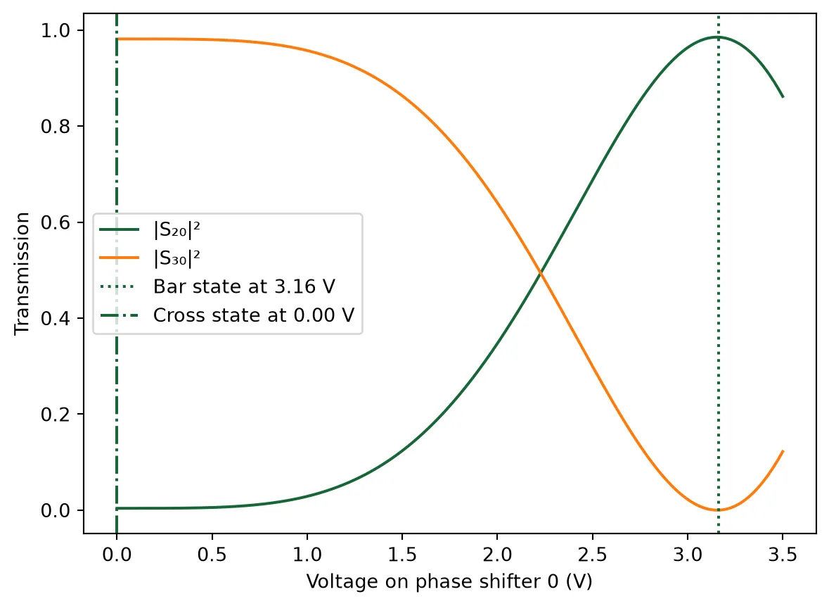
Tunable Unit Cell
Section titled “Tunable Unit Cell”Custom Waveguide Bends and S-Bends
Section titled “Custom Waveguide Bends and S-Bends”We define three types of curved waveguide components to manage routing in this circuit: an S-bend, an extended bend, and a long extended bend. Each path is constructed using arcs and linear segments to ensure smooth transitions and maintain consistent mode propagation.
All components are assigned appropriate ports and use the same complex waveguide model to include propagation loss. These elements will be used in routing scenarios where geometric constraints or thermal tuning paths require customized bending profiles.
# Define an S-bend using arcs and diagonal segments_bend_path = (    pf.Path((0, 0), wg_width)    .arc(180, 135)  # create initial arc    .segment(        (wg_length / 2 - bend_radius, wg_length / 2 - bend_radius),        relative=True,    )  # diagonal segment    .arc(-45, 0)  # final arc to complete S shape)
# Create S-bend component and assign waveguide models_bend = pf.Component("Custom S Bend").add("Si", s_bend_path)s_bend.add_port(s_bend.detect_ports([port_spec]))_ = s_bend.add_model(wg_model, "Waveguide")
# Define a 90-degree bend with extended diagonal segmentbend_path = (    pf.Path((0, 0), wg_width)    .arc(0, 45)  # initial arc    .segment(        (-wg_length / 2 + bend_radius, wg_length / 2 - bend_radius),        relative=True,    )  # diagonal segment    .arc(45, 90)  # final arc to complete the bend)
# Create extended bend component and assign waveguide modelbend = pf.Component("Extended Bend").add("Si", bend_path)bend.add_port(bend.detect_ports([port_spec]))_ = bend.add_model(wg_model, "Waveguide")
# Define a longer bend with extended length and tighter arc overlaplong_bend_length = (    wg_length - bend_radius / 2 - 2 * wg_width)  # calculate diagonal segment lengthlong_bend_path = (    pf.Path((0, 0), wg_width)    .arc(0, 45)  # initial arc    .segment(        (-long_bend_length, long_bend_length),        relative=True,    )  # long diagonal segment    .arc(45, 90)  # final arc)
# Create long bend component and assign waveguide modellong_bend = pf.Component("Long Extended Bend").add("Si", long_bend_path)long_bend.add_port(long_bend.detect_ports([port_spec]))_ = long_bend.add_model(wg_model, "Waveguide")
Constructing a Tunable Unit Cell
Section titled “Constructing a Tunable Unit Cell”We create a tunable unit cell composed of various photonic building blocks: an MZI for modulation, bends, S-bends and waveguides for connectivity. The structure is assembled using a netlist that explicitly defines all component instances, their spatial transformations, and port-level connections.
This modular unit cell forms the basis for scalable switch arrays and can be easily replicated to build larger photonic networks. A circuit model is attached to enable end-to-end simulation of its behavior under voltage-controlled tuning.
netlist_uc = {    "name": "Unit Cell",    "instances": {        "b0": {"component": s_bend, "x_reflection": True},        "wg0": wg,        "mzi": mzi,        "wg1": wg,        "b1": s_bend,        "b2": {"component": bend, "x_reflection": True},        "b3": bend,        "wg2": wg,        "wg3": wg,        "lb0": long_bend,        "lb1": {"component": long_bend, "x_reflection": True},    },    # Explicitly define connections between component ports    "connections": [        (("wg0", "P0"), ("b0", "P1")),        (("mzi", "P1"), ("wg0", "P1")),        (("wg1", "P0"), ("mzi", "P0")),        (("b1", "P0"), ("wg1", "P1")),        (("b2", "P0"), ("mzi", "P2")),        (("b3", "P0"), ("mzi", "P3")),        (("wg2", "P0"), ("b2", "P1")),        (("wg3", "P0"), ("b3", "P1")),        (("lb0", "P0"), ("wg2", "P1")),        (("lb1", "P0"), ("wg3", "P1")),    ],    # Define external ports of the tunable unit    "ports": [("b1", "P1"), ("b0", "P0"), ("lb0", "P1"), ("lb1", "P1")],    # Assign circuit model to the assembled unit    "models": [(pf.CircuitModel(), "Circuit")],}
# Create a photonic component from the defined netlistunit_cell = pf.component_from_netlist(netlist_uc)
# Visualize the assembled tunable unitviewer(unit_cell);fill:%23221f20;font-weight:bold;font-size:10.748952px;}.terminal{fill:none;stroke:%23805080;stroke-width:1.343619;}.dashed{stroke-dasharray:6.718095,4.030857;}.port{fill:none;stroke:%23805080;stroke-width:2.687238;}.virtual-connection{fill:none;stroke:%23907090;stroke-width:2.015429;}.layer_31_0{stroke:%238c78ef;fill:url(%23pat-layer_31_0);fill-opacity:0.492;}.label_31_0{fill:%238c78ef;}.layer_33_0{stroke:%238c78ef;fill:url(%23pat-layer_33_0);fill-opacity:0.492;}.label_33_0{fill:%238c78ef;}.layer_102_0{stroke:%238c78ef;fill:url(%23pat-layer_102_0);fill-opacity:0.492;}.label_102_0{fill:%238c78ef;}.layer_110_0{stroke:%238c78ef;fill:url(%23pat-layer_110_0);fill-opacity:0.492;}.label_110_0{fill:%238c78ef;}.layer_189_0{stroke:%23000000;fill:none;}.label_189_0{fill:%23000000;}.layer_201_0{stroke:%2300ee00;fill:url(%23pat-layer_201_0);fill-opacity:0.492;}.label_201_0{fill:%2300ee00;}.layer_401_0{stroke:%236a8ad2;fill:url(%23pat-layer_401_0);fill-opacity:0.492;}.label_401_0{fill:%236a8ad2;}.layer_202_0{stroke:%23007600;fill:url(%23pat-layer_202_0);fill-opacity:0.492;}.label_202_0{fill:%23007600;}.layer_68_0{stroke:%23008000;fill:url(%23pat-layer_68_0);fill-opacity:0.492;}.label_68_0{fill:%23008000;}.layer_5_0{stroke:%236a8ad2;fill:url(%23pat-layer_5_0);fill-opacity:0.492;}.label_5_0{fill:%236a8ad2;}.layer_998_0{stroke:%23000000;fill:none;}.label_998_0{fill:%23000000;}.layer_312_1{stroke:%2300b8b8;fill:url(%23pat-layer_312_1);fill-opacity:0.492;}.label_312_1{fill:%2300b8b8;}.layer_312_0{stroke:%2300b8b8;fill:url(%23pat-layer_312_0);fill-opacity:0.492;}.label_312_0{fill:%2300b8b8;}.layer_402_0{stroke:%23ff0000;fill:url(%23pat-layer_402_0);fill-opacity:0.492;}.label_402_0{fill:%23ff0000;}.layer_401_4{stroke:%236a8ad2;fill:url(%23pat-layer_401_4);fill-opacity:0.492;}.label_401_4{fill:%236a8ad2;}.layer_389_0{stroke:%23ff00ff;fill:url(%23pat-layer_389_0);fill-opacity:0.492;}.label_389_0{fill:%23ff00ff;}.layer_402_1{stroke:%23ff0000;fill:url(%23pat-layer_402_1);fill-opacity:0.492;}.label_402_1{fill:%23ff0000;}.layer_350_1{stroke:%23697a00;fill:url(%23pat-layer_350_1);fill-opacity:0.492;}.label_350_1{fill:%23697a00;}.layer_401_1{stroke:%236a8ad2;fill:url(%23pat-layer_401_1);fill-opacity:0.492;}.label_401_1{fill:%236a8ad2;}.layer_313_2{stroke:%2301d95b;fill:url(%23pat-layer_313_2);fill-opacity:0.492;}.label_313_2{fill:%2301d95b;}.layer_313_1{stroke:%2301d95b;fill:url(%23pat-layer_313_1);fill-opacity:0.492;}.label_313_1{fill:%2301d95b;}.layer_313_0{stroke:%2301d95b;fill:url(%23pat-layer_313_0);fill-opacity:0.492;}.label_313_0{fill:%2301d95b;}.layer_400_0{stroke:%23a96868;fill:url(%23pat-layer_400_0);fill-opacity:0.492;}.label_400_0{fill:%23a96868;}.layer_312_3{stroke:%2300b8b8;fill:url(%23pat-layer_312_3);fill-opacity:0.492;}.label_312_3{fill:%2300b8b8;}.layer_389_1{stroke:%23ff00ff;fill:url(%23pat-layer_389_1);fill-opacity:0.492;}.label_389_1{fill:%23ff00ff;}.layer_401_3{stroke:%236a8ad2;fill:url(%23pat-layer_401_3);fill-opacity:0.492;}.label_401_3{fill:%236a8ad2;}.layer_403_2{stroke:%23500080;fill:url(%23pat-layer_403_2);fill-opacity:0.492;}.label_403_2{fill:%23500080;}.layer_403_3{stroke:%23500080;fill:url(%23pat-layer_403_3);fill-opacity:0.492;}.label_403_3{fill:%23500080;}.layer_403_1{stroke:%23500080;fill:url(%23pat-layer_403_1);fill-opacity:0.492;}.label_403_1{fill:%23500080;}.layer_403_0{stroke:%23500080;fill:url(%23pat-layer_403_0);fill-opacity:0.492;}.label_403_0{fill:%23500080;}.layer_311_1{stroke:%23ac6c56;fill:url(%23pat-layer_311_1);fill-opacity:0.492;}.label_311_1{fill:%23ac6c56;}.layer_311_0{stroke:%23ac6c56;fill:url(%23pat-layer_311_0);fill-opacity:0.492;}.label_311_0{fill:%23ac6c56;}.layer_301_1{stroke:%23800057;fill:url(%23pat-layer_301_1);fill-opacity:0.492;}.label_301_1{fill:%23800057;}.layer_301_0{stroke:%23800057;fill:url(%23pat-layer_301_0);fill-opacity:0.492;}.label_301_0{fill:%23800057;}.layer_305_1{stroke:%23808080;fill:url(%23pat-layer_305_1);fill-opacity:0.492;}.label_305_1{fill:%23808080;}.layer_305_0{stroke:%23808080;fill:url(%23pat-layer_305_0);fill-opacity:0.492;}.label_305_0{fill:%23808080;}.layer_999_0{stroke:%230000ff;fill:url(%23pat-layer_999_0);fill-opacity:0.492;}.label_999_0{fill:%230000ff;}.layer_81_0{stroke:%23808080;fill:url(%23pat-layer_81_0);fill-opacity:0.492;}.label_81_0{fill:%23808080;}.layer_290_0{stroke:%23a46eda;fill:none;}.label_290_0{fill:%23a46eda;}.layer_205_0{stroke:%2349b203;fill:url(%23pat-layer_205_0);fill-opacity:0.492;}.label_205_0{fill:%2349b203;}.layer_11_0{stroke:%230000ff;fill:url(%23pat-layer_11_0);fill-opacity:0.492;}.label_11_0{fill:%230000ff;}.layer_12_0{stroke:%23a57b00;fill:url(%23pat-layer_12_0);fill-opacity:0.492;}.label_12_0{fill:%23a57b00;}.layer_13_0{stroke:%23800057;fill:url(%23pat-layer_13_0);fill-opacity:0.492;}.label_13_0{fill:%23800057;}.layer_6_0{stroke:%23ff0000;fill:url(%23pat-layer_6_0);fill-opacity:0.492;}.label_6_0{fill:%23ff0000;}.layer_1_10{stroke:%23c96585;fill:url(%23pat-layer_1_10);fill-opacity:0.492;}.label_1_10{fill:%23c96585;}.layer_1_11{stroke:%23800000;fill:url(%23pat-layer_1_11);fill-opacity:0.492;}.label_1_11{fill:%23800000;}.layer_200_0{stroke:%23ff0000;fill:url(%23pat-layer_200_0);fill-opacity:0.492;}.label_200_0{fill:%23ff0000;}.layer_1_0{stroke:%23c96585;fill:url(%23pat-layer_1_0);fill-opacity:0.492;}.label_1_0{fill:%23c96585;}.layer_2_0{stroke:%23a46eda;fill:url(%23pat-layer_2_0);fill-opacity:0.492;}.label_2_0{fill:%23a46eda;}.layer_20_0{stroke:%2353793d;fill:url(%23pat-layer_20_0);fill-opacity:0.492;}.label_20_0{fill:%2353793d;}.layer_22_0{stroke:%23ec7600;fill:url(%23pat-layer_22_0);fill-opacity:0.492;}.label_22_0{fill:%23ec7600;}.layer_24_0{stroke:%2300b8b8;fill:url(%23pat-layer_24_0);fill-opacity:0.492;}.label_24_0{fill:%2300b8b8;}.layer_21_0{stroke:%23736264;fill:url(%23pat-layer_21_0);fill-opacity:0.492;}.label_21_0{fill:%23736264;}.layer_23_0{stroke:%23697a00;fill:url(%23pat-layer_23_0);fill-opacity:0.492;}.label_23_0{fill:%23697a00;}.layer_25_0{stroke:%23008000;fill:url(%23pat-layer_25_0);fill-opacity:0.492;}.label_25_0{fill:%23008000;}.layer_350_0{stroke:%23697a00;fill:url(%23pat-layer_350_0);fill-opacity:0.492;}.label_350_0{fill:%23697a00;}.layer_10_0{stroke:%23000000;fill:none;}.label_10_0{fill:%23000000;}.layer_203_0{stroke:%23008000;fill:url(%23pat-layer_203_0);fill-opacity:0.492;}.label_203_0{fill:%23008000;}.layer_40_0{stroke:%230000ff;fill:url(%23pat-layer_40_0);fill-opacity:0.492;}.label_40_0{fill:%230000ff;}.layer_401_2{stroke:%236a8ad2;fill:url(%23pat-layer_401_2);fill-opacity:0.492;}.label_401_2{fill:%236a8ad2;}.layer_301_2{stroke:%23800057;fill:url(%23pat-layer_301_2);fill-opacity:0.492;}.label_301_2{fill:%23800057;}</style><defs><path id=%22port-symbol%22 class=%22port%22 d=%22M 0,-5.374476 L 8.061714,0 0,5.374476%22 /><path id=%22ref-port-symbol%22 class=%22port%22 style=%22stroke-opacity:0.33;%22 d=%22M 0,-4.030857 C 5.374476,-4.030857 5.374476,4.030857 0,4.030857%22 /><circle id=%22port-bend-symbol%22 style=%22stroke-width:0;stroke:none;fill:%23805080;fill-opacity:1;%22 cx=%220%22 cy=%220%22 r=%222.418514%22 /><circle id=%22connection-symbol%22 style=%22stroke-width:0;stroke:none;fill:%23907090;fill-opacity:1;%22 cx=%220%22 cy=%220%22 r=%222.821600%22 /><pattern id=%22pat-layer_31_0%22 patternUnits=%22userSpaceOnUse%22 width=%226.718095%22 height=%226.718095%22 patternTransform=%22translate(5.137367,6.364511)%22><line x1=%220%22 y1=%220%22 x2=%226.718095%22 y2=%226.718095%22 style=%22stroke:%238c78ef;stroke-width:0.671810%22 /><line x1=%22-3.359048%22 y1=%223.359048%22 x2=%223.359048%22 y2=%2210.077143%22 style=%22stroke:%238c78ef;stroke-width:0.671810%22 /><line x1=%223.359048%22 y1=%22-3.359048%22 x2=%2210.077143%22 y2=%223.359048%22 style=%22stroke:%238c78ef;stroke-width:0.671810%22 /></pattern><pattern id=%22pat-layer_33_0%22 patternUnits=%22userSpaceOnUse%22 width=%226.718095%22 height=%226.718095%22 patternTransform=%22translate(3.951821,0.707168)%22><line x1=%220%22 y1=%220%22 x2=%226.718095%22 y2=%226.718095%22 style=%22stroke:%238c78ef;stroke-width:0.671810%22 /><line x1=%22-3.359048%22 y1=%223.359048%22 x2=%223.359048%22 y2=%2210.077143%22 style=%22stroke:%238c78ef;stroke-width:0.671810%22 /><line x1=%223.359048%22 y1=%22-3.359048%22 x2=%2210.077143%22 y2=%223.359048%22 style=%22stroke:%238c78ef;stroke-width:0.671810%22 /></pattern><pattern id=%22pat-layer_102_0%22 patternUnits=%22userSpaceOnUse%22 width=%226.718095%22 height=%226.718095%22 patternTransform=%22translate(0.000000,0.353584)%22><line x1=%220%22 y1=%220%22 x2=%226.718095%22 y2=%226.718095%22 style=%22stroke:%238c78ef;stroke-width:0.671810%22 /><line x1=%22-3.359048%22 y1=%223.359048%22 x2=%223.359048%22 y2=%2210.077143%22 style=%22stroke:%238c78ef;stroke-width:0.671810%22 /><line x1=%223.359048%22 y1=%22-3.359048%22 x2=%2210.077143%22 y2=%223.359048%22 style=%22stroke:%238c78ef;stroke-width:0.671810%22 /></pattern><pattern id=%22pat-layer_110_0%22 patternUnits=%22userSpaceOnUse%22 width=%226.718095%22 height=%226.718095%22 patternTransform=%22translate(1.975910,4.596591)%22><line x1=%220%22 y1=%220%22 x2=%226.718095%22 y2=%226.718095%22 style=%22stroke:%238c78ef;stroke-width:0.671810%22 /><line x1=%22-3.359048%22 y1=%223.359048%22 x2=%223.359048%22 y2=%2210.077143%22 style=%22stroke:%238c78ef;stroke-width:0.671810%22 /><line x1=%223.359048%22 y1=%22-3.359048%22 x2=%2210.077143%22 y2=%223.359048%22 style=%22stroke:%238c78ef;stroke-width:0.671810%22 /></pattern><pattern id=%22pat-layer_201_0%22 patternUnits=%22userSpaceOnUse%22 width=%226.718095%22 height=%226.718095%22 patternTransform=%22translate(5.137367,2.475088)%22><circle cx=%223.359048%22 cy=%223.359048%22 r=%220.671810%22 style=%22stroke:none;fill:%2300ee00;fill-opacity:1.0%22 /></pattern><pattern id=%22pat-layer_401_0%22 patternUnits=%22userSpaceOnUse%22 width=%224.030857%22 height=%224.030857%22 patternTransform=%22translate(0.474218,0.636451)%22><line x1=%220%22 y1=%220%22 x2=%224.030857%22 y2=%224.030857%22 style=%22stroke:%236a8ad2;stroke-width:0.671810%22 /><line x1=%22-2.015429%22 y1=%222.015429%22 x2=%222.015429%22 y2=%226.046285%22 style=%22stroke:%236a8ad2;stroke-width:0.671810%22 /><line x1=%222.015429%22 y1=%22-2.015429%22 x2=%226.046285%22 y2=%222.015429%22 style=%22stroke:%236a8ad2;stroke-width:0.671810%22 /><line x1=%224.030857%22 y1=%220%22 x2=%220%22 y2=%224.030857%22 style=%22stroke:%236a8ad2;stroke-width:0.671810%22 /><line x1=%226.046285%22 y1=%222.015429%22 x2=%222.015429%22 y2=%226.046285%22 style=%22stroke:%236a8ad2;stroke-width:0.671810%22 /><line x1=%222.015429%22 y1=%22-2.015429%22 x2=%22-2.015429%22 y2=%222.015429%22 style=%22stroke:%236a8ad2;stroke-width:0.671810%22 /></pattern><pattern id=%22pat-layer_202_0%22 patternUnits=%22userSpaceOnUse%22 width=%224.030857%22 height=%224.030857%22 patternTransform=%22translate(0.711328,3.818707)%22><circle cx=%222.015429%22 cy=%222.015429%22 r=%220.671810%22 style=%22stroke:none;fill:%23007600;fill-opacity:1.0%22 /></pattern><pattern id=%22pat-layer_68_0%22 patternUnits=%22userSpaceOnUse%22 width=%226.718095%22 height=%226.718095%22 patternTransform=%22translate(0.000000,2.475088)%22><circle cx=%223.359048%22 cy=%223.359048%22 r=%220.671810%22 style=%22stroke:none;fill:%23008000;fill-opacity:1.0%22 /></pattern><pattern id=%22pat-layer_5_0%22 patternUnits=%22userSpaceOnUse%22 width=%224.030857%22 height=%224.030857%22 patternTransform=%22translate(0.237109,3.606556)%22><line x1=%222.015429%22 y1=%220%22 x2=%222.015429%22 y2=%224.030857%22 style=%22stroke:%236a8ad2;stroke-width:0.671810%22 /></pattern><pattern id=%22pat-layer_312_1%22 patternUnits=%22userSpaceOnUse%22 width=%224.030857%22 height=%224.030857%22 patternTransform=%22translate(0.948437,3.182256)%22><line x1=%220%22 y1=%220%22 x2=%224.030857%22 y2=%224.030857%22 style=%22stroke:%2300b8b8;stroke-width:0.671810%22 /><line x1=%22-2.015429%22 y1=%222.015429%22 x2=%222.015429%22 y2=%226.046285%22 style=%22stroke:%2300b8b8;stroke-width:0.671810%22 /><line x1=%222.015429%22 y1=%22-2.015429%22 x2=%226.046285%22 y2=%222.015429%22 style=%22stroke:%2300b8b8;stroke-width:0.671810%22 /></pattern><pattern id=%22pat-layer_312_0%22 patternUnits=%22userSpaceOnUse%22 width=%226.718095%22 height=%226.718095%22 patternTransform=%22translate(3.161456,4.243007)%22><line x1=%223.359048%22 y1=%220%22 x2=%223.359048%22 y2=%226.718095%22 style=%22stroke:%2300b8b8;stroke-width:0.671810%22 /></pattern><pattern id=%22pat-layer_402_0%22 patternUnits=%22userSpaceOnUse%22 width=%226.718095%22 height=%226.718095%22 patternTransform=%22translate(3.556639,4.950175)%22><line x1=%223.359048%22 y1=%220%22 x2=%223.359048%22 y2=%226.718095%22 style=%22stroke:%23ff0000;stroke-width:0.671810%22 /><line x1=%220%22 y1=%223.359048%22 x2=%226.718095%22 y2=%223.359048%22 style=%22stroke:%23ff0000;stroke-width:0.671810%22 /></pattern><pattern id=%22pat-layer_401_4%22 patternUnits=%22userSpaceOnUse%22 width=%224.030857%22 height=%224.030857%22 patternTransform=%22translate(0.711328,3.182256)%22><line x1=%222.015429%22 y1=%220%22 x2=%222.015429%22 y2=%224.030857%22 style=%22stroke:%236a8ad2;stroke-width:0.671810%22 /></pattern><pattern id=%22pat-layer_389_0%22 patternUnits=%22userSpaceOnUse%22 width=%224.030857%22 height=%224.030857%22 patternTransform=%22translate(0.711328,0.848601)%22><line x1=%222.015429%22 y1=%220%22 x2=%222.015429%22 y2=%224.030857%22 style=%22stroke:%23ff00ff;stroke-width:0.671810%22 /><line x1=%220%22 y1=%222.015429%22 x2=%224.030857%22 y2=%222.015429%22 style=%22stroke:%23ff00ff;stroke-width:0.671810%22 /></pattern><pattern id=%22pat-layer_402_1%22 patternUnits=%22userSpaceOnUse%22 width=%224.030857%22 height=%224.030857%22 patternTransform=%22translate(1.185546,3.606556)%22><line x1=%220%22 y1=%220%22 x2=%224.030857%22 y2=%224.030857%22 style=%22stroke:%23ff0000;stroke-width:0.671810%22 /><line x1=%22-2.015429%22 y1=%222.015429%22 x2=%222.015429%22 y2=%226.046285%22 style=%22stroke:%23ff0000;stroke-width:0.671810%22 /><line x1=%222.015429%22 y1=%22-2.015429%22 x2=%226.046285%22 y2=%222.015429%22 style=%22stroke:%23ff0000;stroke-width:0.671810%22 /><line x1=%224.030857%22 y1=%220%22 x2=%220%22 y2=%224.030857%22 style=%22stroke:%23ff0000;stroke-width:0.671810%22 /><line x1=%226.046285%22 y1=%222.015429%22 x2=%222.015429%22 y2=%226.046285%22 style=%22stroke:%23ff0000;stroke-width:0.671810%22 /><line x1=%222.015429%22 y1=%22-2.015429%22 x2=%22-2.015429%22 y2=%222.015429%22 style=%22stroke:%23ff0000;stroke-width:0.671810%22 /></pattern><pattern id=%22pat-layer_350_1%22 patternUnits=%22userSpaceOnUse%22 width=%224.030857%22 height=%224.030857%22 patternTransform=%22translate(3.556639,3.182256)%22><circle cx=%222.015429%22 cy=%222.015429%22 r=%220.671810%22 style=%22stroke:none;fill:%23697a00;fill-opacity:1.0%22 /></pattern><pattern id=%22pat-layer_401_1%22 patternUnits=%22userSpaceOnUse%22 width=%226.718095%22 height=%226.718095%22 patternTransform=%22translate(5.927731,2.121504)%22><line x1=%220%22 y1=%220%22 x2=%226.718095%22 y2=%226.718095%22 style=%22stroke:%236a8ad2;stroke-width:0.671810%22 /><line x1=%22-3.359048%22 y1=%223.359048%22 x2=%223.359048%22 y2=%2210.077143%22 style=%22stroke:%236a8ad2;stroke-width:0.671810%22 /><line x1=%223.359048%22 y1=%22-3.359048%22 x2=%2210.077143%22 y2=%223.359048%22 style=%22stroke:%236a8ad2;stroke-width:0.671810%22 /><line x1=%226.718095%22 y1=%220%22 x2=%220%22 y2=%226.718095%22 style=%22stroke:%236a8ad2;stroke-width:0.671810%22 /><line x1=%2210.077143%22 y1=%223.359048%22 x2=%223.359048%22 y2=%2210.077143%22 style=%22stroke:%236a8ad2;stroke-width:0.671810%22 /><line x1=%223.359048%22 y1=%22-3.359048%22 x2=%22-3.359048%22 y2=%223.359048%22 style=%22stroke:%236a8ad2;stroke-width:0.671810%22 /></pattern><pattern id=%22pat-layer_313_2%22 patternUnits=%22userSpaceOnUse%22 width=%224.030857%22 height=%224.030857%22 patternTransform=%22translate(1.659765,2.121504)%22><line x1=%220%22 y1=%220%22 x2=%224.030857%22 y2=%224.030857%22 style=%22stroke:%2301d95b;stroke-width:0.671810%22 /><line x1=%22-2.015429%22 y1=%222.015429%22 x2=%222.015429%22 y2=%226.046285%22 style=%22stroke:%2301d95b;stroke-width:0.671810%22 /><line x1=%222.015429%22 y1=%22-2.015429%22 x2=%226.046285%22 y2=%222.015429%22 style=%22stroke:%2301d95b;stroke-width:0.671810%22 /></pattern><pattern id=%22pat-layer_313_1%22 patternUnits=%22userSpaceOnUse%22 width=%226.718095%22 height=%226.718095%22 patternTransform=%22translate(4.347003,2.475088)%22><line x1=%223.359048%22 y1=%220%22 x2=%223.359048%22 y2=%226.718095%22 style=%22stroke:%2301d95b;stroke-width:0.671810%22 /></pattern><pattern id=%22pat-layer_313_0%22 patternUnits=%22userSpaceOnUse%22 width=%224.030857%22 height=%224.030857%22 patternTransform=%22translate(3.556639,0.848601)%22><line x1=%222.015429%22 y1=%220%22 x2=%222.015429%22 y2=%224.030857%22 style=%22stroke:%2301d95b;stroke-width:0.671810%22 /></pattern><pattern id=%22pat-layer_400_0%22 patternUnits=%22userSpaceOnUse%22 width=%226.718095%22 height=%226.718095%22 patternTransform=%22translate(4.742185,3.889423)%22><line x1=%220%22 y1=%220%22 x2=%226.718095%22 y2=%226.718095%22 style=%22stroke:%23a96868;stroke-width:0.671810%22 /><line x1=%22-3.359048%22 y1=%223.359048%22 x2=%223.359048%22 y2=%2210.077143%22 style=%22stroke:%23a96868;stroke-width:0.671810%22 /><line x1=%223.359048%22 y1=%22-3.359048%22 x2=%2210.077143%22 y2=%223.359048%22 style=%22stroke:%23a96868;stroke-width:0.671810%22 /><line x1=%226.718095%22 y1=%220%22 x2=%220%22 y2=%226.718095%22 style=%22stroke:%23a96868;stroke-width:0.671810%22 /><line x1=%2210.077143%22 y1=%223.359048%22 x2=%223.359048%22 y2=%2210.077143%22 style=%22stroke:%23a96868;stroke-width:0.671810%22 /><line x1=%223.359048%22 y1=%22-3.359048%22 x2=%22-3.359048%22 y2=%223.359048%22 style=%22stroke:%23a96868;stroke-width:0.671810%22 /></pattern><pattern id=%22pat-layer_312_3%22 patternUnits=%22userSpaceOnUse%22 width=%224.030857%22 height=%224.030857%22 patternTransform=%22translate(3.082420,0.424301)%22><line x1=%224.030857%22 y1=%220%22 x2=%220%22 y2=%224.030857%22 style=%22stroke:%2300b8b8;stroke-width:0.671810%22 /><line x1=%226.046285%22 y1=%222.015429%22 x2=%222.015429%22 y2=%226.046285%22 style=%22stroke:%2300b8b8;stroke-width:0.671810%22 /><line x1=%222.015429%22 y1=%22-2.015429%22 x2=%22-2.015429%22 y2=%222.015429%22 style=%22stroke:%2300b8b8;stroke-width:0.671810%22 /></pattern><pattern id=%22pat-layer_389_1%22 patternUnits=%22userSpaceOnUse%22 width=%226.718095%22 height=%226.718095%22 patternTransform=%22translate(6.322913,2.475088)%22><line x1=%223.359048%22 y1=%220%22 x2=%223.359048%22 y2=%226.718095%22 style=%22stroke:%23ff00ff;stroke-width:0.671810%22 /><line x1=%220%22 y1=%223.359048%22 x2=%226.718095%22 y2=%223.359048%22 style=%22stroke:%23ff00ff;stroke-width:0.671810%22 /></pattern><pattern id=%22pat-layer_401_3%22 patternUnits=%22userSpaceOnUse%22 width=%226.718095%22 height=%226.718095%22 patternTransform=%22translate(2.766274,4.243007)%22><line x1=%220%22 y1=%223.359048%22 x2=%226.718095%22 y2=%223.359048%22 style=%22stroke:%236a8ad2;stroke-width:0.671810%22 /></pattern><pattern id=%22pat-layer_403_2%22 patternUnits=%22userSpaceOnUse%22 width=%224.030857%22 height=%224.030857%22 patternTransform=%22translate(1.896874,2.545804)%22><line x1=%220%22 y1=%220%22 x2=%224.030857%22 y2=%224.030857%22 style=%22stroke:%23500080;stroke-width:0.671810%22 /><line x1=%22-2.015429%22 y1=%222.015429%22 x2=%222.015429%22 y2=%226.046285%22 style=%22stroke:%23500080;stroke-width:0.671810%22 /><line x1=%222.015429%22 y1=%22-2.015429%22 x2=%226.046285%22 y2=%222.015429%22 style=%22stroke:%23500080;stroke-width:0.671810%22 /><line x1=%224.030857%22 y1=%220%22 x2=%220%22 y2=%224.030857%22 style=%22stroke:%23500080;stroke-width:0.671810%22 /><line x1=%226.046285%22 y1=%222.015429%22 x2=%222.015429%22 y2=%226.046285%22 style=%22stroke:%23500080;stroke-width:0.671810%22 /><line x1=%222.015429%22 y1=%22-2.015429%22 x2=%22-2.015429%22 y2=%222.015429%22 style=%22stroke:%23500080;stroke-width:0.671810%22 /></pattern><pattern id=%22pat-layer_403_3%22 patternUnits=%22userSpaceOnUse%22 width=%226.718095%22 height=%226.718095%22 patternTransform=%22translate(1.580728,5.303759)%22><line x1=%220%22 y1=%220%22 x2=%226.718095%22 y2=%226.718095%22 style=%22stroke:%23500080;stroke-width:0.671810%22 /><line x1=%22-3.359048%22 y1=%223.359048%22 x2=%223.359048%22 y2=%2210.077143%22 style=%22stroke:%23500080;stroke-width:0.671810%22 /><line x1=%223.359048%22 y1=%22-3.359048%22 x2=%2210.077143%22 y2=%223.359048%22 style=%22stroke:%23500080;stroke-width:0.671810%22 /><line x1=%226.718095%22 y1=%220%22 x2=%220%22 y2=%226.718095%22 style=%22stroke:%23500080;stroke-width:0.671810%22 /><line x1=%2210.077143%22 y1=%223.359048%22 x2=%223.359048%22 y2=%2210.077143%22 style=%22stroke:%23500080;stroke-width:0.671810%22 /><line x1=%223.359048%22 y1=%22-3.359048%22 x2=%22-3.359048%22 y2=%223.359048%22 style=%22stroke:%23500080;stroke-width:0.671810%22 /></pattern><pattern id=%22pat-layer_403_1%22 patternUnits=%22userSpaceOnUse%22 width=%226.718095%22 height=%226.718095%22 patternTransform=%22translate(4.742185,3.182256)%22><line x1=%223.359048%22 y1=%220%22 x2=%223.359048%22 y2=%226.718095%22 style=%22stroke:%23500080;stroke-width:0.671810%22 /><line x1=%220%22 y1=%223.359048%22 x2=%226.718095%22 y2=%223.359048%22 style=%22stroke:%23500080;stroke-width:0.671810%22 /></pattern><pattern id=%22pat-layer_403_0%22 patternUnits=%22userSpaceOnUse%22 width=%224.030857%22 height=%224.030857%22 patternTransform=%22translate(3.793748,1.272902)%22><line x1=%222.015429%22 y1=%220%22 x2=%222.015429%22 y2=%224.030857%22 style=%22stroke:%23500080;stroke-width:0.671810%22 /><line x1=%220%22 y1=%222.015429%22 x2=%224.030857%22 y2=%222.015429%22 style=%22stroke:%23500080;stroke-width:0.671810%22 /></pattern><pattern id=%22pat-layer_311_1%22 patternUnits=%22userSpaceOnUse%22 width=%226.718095%22 height=%226.718095%22 patternTransform=%22translate(5.532549,1.414336)%22><line x1=%220%22 y1=%220%22 x2=%226.718095%22 y2=%226.718095%22 style=%22stroke:%23ac6c56;stroke-width:0.671810%22 /><line x1=%22-3.359048%22 y1=%223.359048%22 x2=%223.359048%22 y2=%2210.077143%22 style=%22stroke:%23ac6c56;stroke-width:0.671810%22 /><line x1=%223.359048%22 y1=%22-3.359048%22 x2=%2210.077143%22 y2=%223.359048%22 style=%22stroke:%23ac6c56;stroke-width:0.671810%22 /></pattern><pattern id=%22pat-layer_311_0%22 patternUnits=%22userSpaceOnUse%22 width=%224.030857%22 height=%224.030857%22 patternTransform=%22translate(0.237109,0.212150)%22><line x1=%220%22 y1=%220%22 x2=%224.030857%22 y2=%224.030857%22 style=%22stroke:%23ac6c56;stroke-width:0.671810%22 /><line x1=%22-2.015429%22 y1=%222.015429%22 x2=%222.015429%22 y2=%226.046285%22 style=%22stroke:%23ac6c56;stroke-width:0.671810%22 /><line x1=%222.015429%22 y1=%22-2.015429%22 x2=%226.046285%22 y2=%222.015429%22 style=%22stroke:%23ac6c56;stroke-width:0.671810%22 /></pattern><pattern id=%22pat-layer_301_1%22 patternUnits=%22userSpaceOnUse%22 width=%226.718095%22 height=%226.718095%22 patternTransform=%22translate(4.742185,2.828672)%22><line x1=%220%22 y1=%223.359048%22 x2=%226.718095%22 y2=%223.359048%22 style=%22stroke:%23800057;stroke-width:0.671810%22 /></pattern><pattern id=%22pat-layer_301_0%22 patternUnits=%22userSpaceOnUse%22 width=%224.030857%22 height=%224.030857%22 patternTransform=%22translate(3.793748,1.060752)%22><line x1=%220%22 y1=%222.015429%22 x2=%224.030857%22 y2=%222.015429%22 style=%22stroke:%23800057;stroke-width:0.671810%22 /></pattern><pattern id=%22pat-layer_305_1%22 patternUnits=%22userSpaceOnUse%22 width=%226.718095%22 height=%226.718095%22 patternTransform=%22translate(2.371092,4.950175)%22><line x1=%223.359048%22 y1=%220%22 x2=%223.359048%22 y2=%226.718095%22 style=%22stroke:%23808080;stroke-width:0.671810%22 /><line x1=%220%22 y1=%223.359048%22 x2=%226.718095%22 y2=%223.359048%22 style=%22stroke:%23808080;stroke-width:0.671810%22 /></pattern><pattern id=%22pat-layer_305_0%22 patternUnits=%22userSpaceOnUse%22 width=%224.030857%22 height=%224.030857%22 patternTransform=%22translate(2.371092,2.333654)%22><line x1=%222.015429%22 y1=%220%22 x2=%222.015429%22 y2=%224.030857%22 style=%22stroke:%23808080;stroke-width:0.671810%22 /><line x1=%220%22 y1=%222.015429%22 x2=%224.030857%22 y2=%222.015429%22 style=%22stroke:%23808080;stroke-width:0.671810%22 /></pattern><pattern id=%22pat-layer_999_0%22 patternUnits=%22userSpaceOnUse%22 width=%224.030857%22 height=%224.030857%22 patternTransform=%22translate(1.422655,1.485053)%22><line x1=%222.015429%22 y1=%220%22 x2=%222.015429%22 y2=%224.030857%22 style=%22stroke:%230000ff;stroke-width:0.671810%22 /></pattern><pattern id=%22pat-layer_81_0%22 patternUnits=%22userSpaceOnUse%22 width=%224.030857%22 height=%224.030857%22 patternTransform=%22translate(1.422655,3.606556)%22><line x1=%222.015429%22 y1=%220%22 x2=%222.015429%22 y2=%224.030857%22 style=%22stroke:%23808080;stroke-width:0.671810%22 /><line x1=%220%22 y1=%222.015429%22 x2=%224.030857%22 y2=%222.015429%22 style=%22stroke:%23808080;stroke-width:0.671810%22 /></pattern><pattern id=%22pat-layer_205_0%22 patternUnits=%22userSpaceOnUse%22 width=%224.030857%22 height=%224.030857%22 patternTransform=%22translate(1.659765,2.757955)%22><line x1=%220%22 y1=%220%22 x2=%224.030857%22 y2=%224.030857%22 style=%22stroke:%2349b203;stroke-width:0.671810%22 /><line x1=%22-2.015429%22 y1=%222.015429%22 x2=%222.015429%22 y2=%226.046285%22 style=%22stroke:%2349b203;stroke-width:0.671810%22 /><line x1=%222.015429%22 y1=%22-2.015429%22 x2=%226.046285%22 y2=%222.015429%22 style=%22stroke:%2349b203;stroke-width:0.671810%22 /><line x1=%224.030857%22 y1=%220%22 x2=%220%22 y2=%224.030857%22 style=%22stroke:%2349b203;stroke-width:0.671810%22 /><line x1=%226.046285%22 y1=%222.015429%22 x2=%222.015429%22 y2=%226.046285%22 style=%22stroke:%2349b203;stroke-width:0.671810%22 /><line x1=%222.015429%22 y1=%22-2.015429%22 x2=%22-2.015429%22 y2=%222.015429%22 style=%22stroke:%2349b203;stroke-width:0.671810%22 /></pattern><pattern id=%22pat-layer_11_0%22 patternUnits=%22userSpaceOnUse%22 width=%224.030857%22 height=%224.030857%22 patternTransform=%22translate(2.133983,1.485053)%22><line x1=%224.030857%22 y1=%220%22 x2=%220%22 y2=%224.030857%22 style=%22stroke:%230000ff;stroke-width:0.671810%22 /><line x1=%226.046285%22 y1=%222.015429%22 x2=%222.015429%22 y2=%226.046285%22 style=%22stroke:%230000ff;stroke-width:0.671810%22 /><line x1=%222.015429%22 y1=%22-2.015429%22 x2=%22-2.015429%22 y2=%222.015429%22 style=%22stroke:%230000ff;stroke-width:0.671810%22 /></pattern><pattern id=%22pat-layer_12_0%22 patternUnits=%22userSpaceOnUse%22 width=%224.030857%22 height=%224.030857%22 patternTransform=%22translate(3.793748,3.818707)%22><line x1=%220%22 y1=%220%22 x2=%224.030857%22 y2=%224.030857%22 style=%22stroke:%23a57b00;stroke-width:0.671810%22 /><line x1=%22-2.015429%22 y1=%222.015429%22 x2=%222.015429%22 y2=%226.046285%22 style=%22stroke:%23a57b00;stroke-width:0.671810%22 /><line x1=%222.015429%22 y1=%22-2.015429%22 x2=%226.046285%22 y2=%222.015429%22 style=%22stroke:%23a57b00;stroke-width:0.671810%22 /></pattern><pattern id=%22pat-layer_13_0%22 patternUnits=%22userSpaceOnUse%22 width=%224.030857%22 height=%224.030857%22 patternTransform=%22translate(1.422655,2.121504)%22><line x1=%224.030857%22 y1=%220%22 x2=%220%22 y2=%224.030857%22 style=%22stroke:%23800057;stroke-width:0.671810%22 /><line x1=%226.046285%22 y1=%222.015429%22 x2=%222.015429%22 y2=%226.046285%22 style=%22stroke:%23800057;stroke-width:0.671810%22 /><line x1=%222.015429%22 y1=%22-2.015429%22 x2=%22-2.015429%22 y2=%222.015429%22 style=%22stroke:%23800057;stroke-width:0.671810%22 /></pattern><pattern id=%22pat-layer_6_0%22 patternUnits=%22userSpaceOnUse%22 width=%226.718095%22 height=%226.718095%22 patternTransform=%22translate(3.161456,3.182256)%22><line x1=%220%22 y1=%223.359048%22 x2=%226.718095%22 y2=%223.359048%22 style=%22stroke:%23ff0000;stroke-width:0.671810%22 /></pattern><pattern id=%22pat-layer_1_10%22 patternUnits=%22userSpaceOnUse%22 width=%224.030857%22 height=%224.030857%22 patternTransform=%22translate(0.237109,0.636451)%22><line x1=%220%22 y1=%220%22 x2=%224.030857%22 y2=%224.030857%22 style=%22stroke:%23c96585;stroke-width:0.671810%22 /><line x1=%22-2.015429%22 y1=%222.015429%22 x2=%222.015429%22 y2=%226.046285%22 style=%22stroke:%23c96585;stroke-width:0.671810%22 /><line x1=%222.015429%22 y1=%22-2.015429%22 x2=%226.046285%22 y2=%222.015429%22 style=%22stroke:%23c96585;stroke-width:0.671810%22 /><line x1=%224.030857%22 y1=%220%22 x2=%220%22 y2=%224.030857%22 style=%22stroke:%23c96585;stroke-width:0.671810%22 /><line x1=%226.046285%22 y1=%222.015429%22 x2=%222.015429%22 y2=%226.046285%22 style=%22stroke:%23c96585;stroke-width:0.671810%22 /><line x1=%222.015429%22 y1=%22-2.015429%22 x2=%22-2.015429%22 y2=%222.015429%22 style=%22stroke:%23c96585;stroke-width:0.671810%22 /></pattern><pattern id=%22pat-layer_1_11%22 patternUnits=%22userSpaceOnUse%22 width=%226.718095%22 height=%226.718095%22 patternTransform=%22translate(5.532549,2.121504)%22><line x1=%223.359048%22 y1=%220%22 x2=%223.359048%22 y2=%226.718095%22 style=%22stroke:%23800000;stroke-width:0.671810%22 /><line x1=%220%22 y1=%223.359048%22 x2=%226.718095%22 y2=%223.359048%22 style=%22stroke:%23800000;stroke-width:0.671810%22 /></pattern><pattern id=%22pat-layer_200_0%22 patternUnits=%22userSpaceOnUse%22 width=%226.718095%22 height=%226.718095%22 patternTransform=%22translate(2.371092,5.303759)%22><line x1=%220%22 y1=%220%22 x2=%226.718095%22 y2=%226.718095%22 style=%22stroke:%23ff0000;stroke-width:0.671810%22 /><line x1=%22-3.359048%22 y1=%223.359048%22 x2=%223.359048%22 y2=%2210.077143%22 style=%22stroke:%23ff0000;stroke-width:0.671810%22 /><line x1=%223.359048%22 y1=%22-3.359048%22 x2=%2210.077143%22 y2=%223.359048%22 style=%22stroke:%23ff0000;stroke-width:0.671810%22 /><line x1=%226.718095%22 y1=%220%22 x2=%220%22 y2=%226.718095%22 style=%22stroke:%23ff0000;stroke-width:0.671810%22 /><line x1=%2210.077143%22 y1=%223.359048%22 x2=%223.359048%22 y2=%2210.077143%22 style=%22stroke:%23ff0000;stroke-width:0.671810%22 /><line x1=%223.359048%22 y1=%22-3.359048%22 x2=%22-3.359048%22 y2=%223.359048%22 style=%22stroke:%23ff0000;stroke-width:0.671810%22 /></pattern><pattern id=%22pat-layer_1_0%22 patternUnits=%22userSpaceOnUse%22 width=%224.030857%22 height=%224.030857%22 patternTransform=%22translate(1.659765,2.333654)%22><line x1=%224.030857%22 y1=%220%22 x2=%220%22 y2=%224.030857%22 style=%22stroke:%23c96585;stroke-width:0.671810%22 /><line x1=%226.046285%22 y1=%222.015429%22 x2=%222.015429%22 y2=%226.046285%22 style=%22stroke:%23c96585;stroke-width:0.671810%22 /><line x1=%222.015429%22 y1=%22-2.015429%22 x2=%22-2.015429%22 y2=%222.015429%22 style=%22stroke:%23c96585;stroke-width:0.671810%22 /></pattern><pattern id=%22pat-layer_2_0%22 patternUnits=%22userSpaceOnUse%22 width=%226.718095%22 height=%226.718095%22 patternTransform=%22translate(5.532549,1.060752)%22><line x1=%220%22 y1=%220%22 x2=%226.718095%22 y2=%226.718095%22 style=%22stroke:%23a46eda;stroke-width:0.671810%22 /><line x1=%22-3.359048%22 y1=%223.359048%22 x2=%223.359048%22 y2=%2210.077143%22 style=%22stroke:%23a46eda;stroke-width:0.671810%22 /><line x1=%223.359048%22 y1=%22-3.359048%22 x2=%2210.077143%22 y2=%223.359048%22 style=%22stroke:%23a46eda;stroke-width:0.671810%22 /></pattern><pattern id=%22pat-layer_20_0%22 patternUnits=%22userSpaceOnUse%22 width=%226.718095%22 height=%226.718095%22 patternTransform=%22translate(1.580728,3.889423)%22><line x1=%220%22 y1=%223.359048%22 x2=%226.718095%22 y2=%223.359048%22 style=%22stroke:%2353793d;stroke-width:0.671810%22 /></pattern><pattern id=%22pat-layer_22_0%22 patternUnits=%22userSpaceOnUse%22 width=%226.718095%22 height=%226.718095%22 patternTransform=%22translate(0.395182,4.950175)%22><line x1=%220%22 y1=%220%22 x2=%226.718095%22 y2=%226.718095%22 style=%22stroke:%23ec7600;stroke-width:0.671810%22 /><line x1=%22-3.359048%22 y1=%223.359048%22 x2=%223.359048%22 y2=%2210.077143%22 style=%22stroke:%23ec7600;stroke-width:0.671810%22 /><line x1=%223.359048%22 y1=%22-3.359048%22 x2=%2210.077143%22 y2=%223.359048%22 style=%22stroke:%23ec7600;stroke-width:0.671810%22 /><line x1=%226.718095%22 y1=%220%22 x2=%220%22 y2=%226.718095%22 style=%22stroke:%23ec7600;stroke-width:0.671810%22 /><line x1=%2210.077143%22 y1=%223.359048%22 x2=%223.359048%22 y2=%2210.077143%22 style=%22stroke:%23ec7600;stroke-width:0.671810%22 /><line x1=%223.359048%22 y1=%22-3.359048%22 x2=%22-3.359048%22 y2=%223.359048%22 style=%22stroke:%23ec7600;stroke-width:0.671810%22 /></pattern><pattern id=%22pat-layer_24_0%22 patternUnits=%22userSpaceOnUse%22 width=%226.718095%22 height=%226.718095%22 patternTransform=%22translate(5.927731,6.010927)%22><line x1=%223.359048%22 y1=%220%22 x2=%223.359048%22 y2=%226.718095%22 style=%22stroke:%2300b8b8;stroke-width:0.671810%22 /><line x1=%220%22 y1=%223.359048%22 x2=%226.718095%22 y2=%223.359048%22 style=%22stroke:%2300b8b8;stroke-width:0.671810%22 /></pattern><pattern id=%22pat-layer_21_0%22 patternUnits=%22userSpaceOnUse%22 width=%224.030857%22 height=%224.030857%22 patternTransform=%22translate(2.608202,0.636451)%22><line x1=%220%22 y1=%222.015429%22 x2=%224.030857%22 y2=%222.015429%22 style=%22stroke:%23736264;stroke-width:0.671810%22 /></pattern><pattern id=%22pat-layer_23_0%22 patternUnits=%22userSpaceOnUse%22 width=%224.030857%22 height=%224.030857%22 patternTransform=%22translate(1.896874,1.272902)%22><line x1=%220%22 y1=%220%22 x2=%224.030857%22 y2=%224.030857%22 style=%22stroke:%23697a00;stroke-width:0.671810%22 /><line x1=%22-2.015429%22 y1=%222.015429%22 x2=%222.015429%22 y2=%226.046285%22 style=%22stroke:%23697a00;stroke-width:0.671810%22 /><line x1=%222.015429%22 y1=%22-2.015429%22 x2=%226.046285%22 y2=%222.015429%22 style=%22stroke:%23697a00;stroke-width:0.671810%22 /><line x1=%224.030857%22 y1=%220%22 x2=%220%22 y2=%224.030857%22 style=%22stroke:%23697a00;stroke-width:0.671810%22 /><line x1=%226.046285%22 y1=%222.015429%22 x2=%222.015429%22 y2=%226.046285%22 style=%22stroke:%23697a00;stroke-width:0.671810%22 /><line x1=%222.015429%22 y1=%22-2.015429%22 x2=%22-2.015429%22 y2=%222.015429%22 style=%22stroke:%23697a00;stroke-width:0.671810%22 /></pattern><pattern id=%22pat-layer_25_0%22 patternUnits=%22userSpaceOnUse%22 width=%224.030857%22 height=%224.030857%22 patternTransform=%22translate(1.185546,1.909353)%22><line x1=%222.015429%22 y1=%220%22 x2=%222.015429%22 y2=%224.030857%22 style=%22stroke:%23008000;stroke-width:0.671810%22 /><line x1=%220%22 y1=%222.015429%22 x2=%224.030857%22 y2=%222.015429%22 style=%22stroke:%23008000;stroke-width:0.671810%22 /></pattern><pattern id=%22pat-layer_350_0%22 patternUnits=%22userSpaceOnUse%22 width=%226.718095%22 height=%226.718095%22 patternTransform=%22translate(0.790364,4.243007)%22><line x1=%226.718095%22 y1=%220%22 x2=%220%22 y2=%226.718095%22 style=%22stroke:%23697a00;stroke-width:0.671810%22 /><line x1=%2210.077143%22 y1=%223.359048%22 x2=%223.359048%22 y2=%2210.077143%22 style=%22stroke:%23697a00;stroke-width:0.671810%22 /><line x1=%223.359048%22 y1=%22-3.359048%22 x2=%22-3.359048%22 y2=%223.359048%22 style=%22stroke:%23697a00;stroke-width:0.671810%22 /></pattern><pattern id=%22pat-layer_203_0%22 patternUnits=%22userSpaceOnUse%22 width=%226.718095%22 height=%226.718095%22 patternTransform=%22translate(3.951821,3.535839)%22><line x1=%226.718095%22 y1=%220%22 x2=%220%22 y2=%226.718095%22 style=%22stroke:%23008000;stroke-width:0.671810%22 /><line x1=%2210.077143%22 y1=%223.359048%22 x2=%223.359048%22 y2=%2210.077143%22 style=%22stroke:%23008000;stroke-width:0.671810%22 /><line x1=%223.359048%22 y1=%22-3.359048%22 x2=%22-3.359048%22 y2=%223.359048%22 style=%22stroke:%23008000;stroke-width:0.671810%22 /></pattern><pattern id=%22pat-layer_40_0%22 patternUnits=%22userSpaceOnUse%22 width=%226.718095%22 height=%226.718095%22 patternTransform=%22translate(3.161456,1.060752)%22><circle cx=%223.359048%22 cy=%223.359048%22 r=%220.671810%22 style=%22stroke:none;fill:%230000ff;fill-opacity:1.0%22 /></pattern><pattern id=%22pat-layer_401_2%22 patternUnits=%22userSpaceOnUse%22 width=%224.030857%22 height=%224.030857%22 patternTransform=%22translate(2.608202,1.909353)%22><line x1=%220%22 y1=%222.015429%22 x2=%224.030857%22 y2=%222.015429%22 style=%22stroke:%236a8ad2;stroke-width:0.671810%22 /></pattern><pattern id=%22pat-layer_301_2%22 patternUnits=%22userSpaceOnUse%22 width=%224.030857%22 height=%224.030857%22 patternTransform=%22translate(1.896874,2.333654)%22><line x1=%222.015429%22 y1=%220%22 x2=%222.015429%22 y2=%224.030857%22 style=%22stroke:%23800057;stroke-width:0.671810%22 /></pattern><g id=%22C1%22 data-name=%22Custom S Bend%22><path class=%22layer_1_0%22 d=%22M 0.215000,0.000000 0.224000,0.989000 0.245000,1.479000 0.287000,1.964000 0.355000,2.443000 0.454000,2.915000 0.589000,3.377000 0.756000,3.829000 0.957000,4.267000 1.189000,4.689000 1.452000,5.093000 1.743000,5.479000 2.057000,5.852000 2.388000,6.213000 3.081000,6.919000 28.081000,31.919000 28.782000,32.633000 29.123000,33.006000 29.451000,33.394000 29.758000,33.802000 30.038000,34.232000 30.285000,34.682000 30.499000,35.149000 30.678000,35.630000 30.821000,36.123000 30.927000,36.625000 30.998000,37.131000 31.042000,37.637000 31.064000,38.141000 31.073000,39.142000 30.643000,39.142000 30.634000,38.153000 30.612000,37.663000 30.571000,37.178000 30.503000,36.699000 30.404000,36.227000 30.269000,35.765000 30.102000,35.313000 29.901000,34.875000 29.669000,34.453000 29.406000,34.050000 29.115000,33.663000 28.801000,33.290000 28.470000,32.929000 27.777000,32.223000 2.777000,7.223000 2.076000,6.509000 1.735000,6.136000 1.407000,5.748000 1.100000,5.340000 0.820000,4.910000 0.573000,4.460000 0.359000,3.993000 0.180000,3.512000 0.037000,3.019000 -0.069000,2.517000 -0.140000,2.012000 -0.184000,1.505000 -0.206000,1.001000 -0.215000,0.000000 z%22 /></g><g id=%22C2%22 data-name=%22wg%22><path class=%22layer_1_0%22 d=%22M 0.000000,-0.215000 70.000000,-0.215000 70.000000,0.215000 0.000000,0.215000 z%22 /></g><g id=%22C3%22 data-name=%22Tunable MZI%22><use transform=%22translate(0.000000 0.000000)%22 href=%22%23C6%22 /><use transform=%22translate(42.300000 -45.750000)%22 href=%22%23C7%22 /><use transform=%22translate(42.300000 35.000000)%22 href=%22%23C7%22 /><use transform=%22translate(154.600000 0.000000)%22 href=%22%23C6%22 /><use transform=%22translate(0.000000 0.000000)%22 href=%22%23C8%22 /><use transform=%22translate(0.000000 0.000000)%22 href=%22%23C9%22 /><use transform=%22translate(0.000000 0.000000)%22 href=%22%23C10%22 /><use transform=%22translate(0.000000 0.000000)%22 href=%22%23C11%22 /></g><g id=%22C4%22 data-name=%22Extended Bend%22><path class=%22layer_1_0%22 d=%22M 0.215000,0.000000 0.206000,1.001000 0.184000,1.505000 0.140000,2.012000 0.069000,2.517000 -0.037000,3.019000 -0.180000,3.512000 -0.359000,3.993000 -0.573000,4.460000 -0.820000,4.910000 -1.100000,5.340000 -1.407000,5.748000 -1.735000,6.136000 -2.076000,6.509000 -2.777000,7.223000 -27.777000,32.223000 -28.491000,32.924000 -28.864000,33.265000 -29.252000,33.593000 -29.660000,33.900000 -30.090000,34.180000 -30.540000,34.427000 -31.007000,34.641000 -31.488000,34.820000 -31.981000,34.963000 -32.483000,35.069000 -32.989000,35.140000 -33.495000,35.184000 -33.999000,35.206000 -35.000000,35.215000 -35.000000,34.785000 -34.011000,34.776000 -33.521000,34.754000 -33.036000,34.713000 -32.557000,34.645000 -32.085000,34.546000 -31.623000,34.411000 -31.171000,34.244000 -30.733000,34.043000 -30.311000,33.811000 -29.908000,33.548000 -29.521000,33.257000 -29.148000,32.943000 -28.787000,32.612000 -28.081000,31.919000 -3.081000,6.919000 -2.388000,6.213000 -2.057000,5.852000 -1.743000,5.479000 -1.452000,5.093000 -1.189000,4.689000 -0.957000,4.267000 -0.756000,3.829000 -0.589000,3.377000 -0.454000,2.915000 -0.355000,2.443000 -0.287000,1.964000 -0.245000,1.479000 -0.224000,0.989000 -0.215000,0.000000 z%22 /></g><g id=%22C5%22 data-name=%22Long Extended Bend%22><path class=%22layer_1_0%22 d=%22M 0.215000,0.000000 0.206000,1.001000 0.184000,1.505000 0.140000,2.012000 0.069000,2.517000 -0.037000,3.019000 -0.180000,3.512000 -0.359000,3.993000 -0.573000,4.460000 -0.820000,4.910000 -1.100000,5.340000 -1.407000,5.748000 -1.735000,6.136000 -2.076000,6.509000 -2.777000,7.223000 -66.917000,71.363000 -67.631000,72.064000 -68.004000,72.405000 -68.392000,72.733000 -68.800000,73.040000 -69.230000,73.320000 -69.680000,73.567000 -70.147000,73.781000 -70.628000,73.960000 -71.121000,74.103000 -71.623000,74.209000 -72.129000,74.280000 -72.635000,74.324000 -73.139000,74.346000 -74.140000,74.355000 -74.140000,73.925000 -73.151000,73.916000 -72.661000,73.894000 -72.176000,73.853000 -71.697000,73.785000 -71.225000,73.686000 -70.763000,73.551000 -70.311000,73.384000 -69.873000,73.183000 -69.451000,72.951000 -69.048000,72.688000 -68.661000,72.397000 -68.288000,72.083000 -67.927000,71.752000 -67.221000,71.059000 -3.081000,6.919000 -2.388000,6.213000 -2.057000,5.852000 -1.743000,5.479000 -1.452000,5.093000 -1.189000,4.689000 -0.957000,4.267000 -0.756000,3.829000 -0.589000,3.377000 -0.454000,2.915000 -0.355000,2.443000 -0.287000,1.964000 -0.245000,1.479000 -0.224000,0.989000 -0.215000,0.000000 z%22 /></g><g id=%22C10%22 data-name=%22route__6X47YPFGQRPBJVZ7BN52QB2ERLBKKXRAPQG6REFJZU6V5AN2ZHWA%22><use transform=%22translate(139.200000 0.000000) rotate(90.000000)%22 href=%22%23C12%22 /><use transform=%22translate(139.200000 25.000000) rotate(90.000000)%22 href=%22%23C13%22 /><use transform=%22translate(129.200000 35.000000) rotate(180.000000)%22 href=%22%23C14%22 /></g><g id=%22C11%22 data-name=%22route__4BKV7ZXGVAYW6RZFRUUHCEVW44YY5UNN6TMI76ELNQ5PHQZYR7FQ%22><use transform=%22translate(139.200000 -10.750000) rotate(270.000000)%22 href=%22%23C12%22 /><use transform=%22translate(139.200000 -35.750000) rotate(270.000000)%22 href=%22%23C15%22 /><use transform=%22translate(129.200000 -45.750000) rotate(180.000000)%22 href=%22%23C14%22 /></g><g id=%22C6%22 data-name=%22dual_ring_coupler__3B34D4GMHE6HXHZXGRWFOIZFKMLHKUUMDA7FHTLY67P6BNNHGW3A%22><path class=%22layer_1_0%22 d=%22M -15.185000,-10.750000 -15.183000,-10.233000 -15.166000,-9.722000 -15.122000,-9.219000 -15.086000,-8.972000 -15.038000,-8.728000 -14.977000,-8.488000 -14.901000,-8.254000 -14.810000,-8.027000 -14.703000,-7.808000 -14.580000,-7.597000 -14.442000,-7.396000 -14.290000,-7.205000 -14.124000,-7.026000 -13.945000,-6.860000 -13.754000,-6.708000 -13.553000,-6.570000 -13.342000,-6.447000 -13.123000,-6.340000 -12.896000,-6.249000 -12.662000,-6.173000 -12.422000,-6.112000 -12.178000,-6.064000 -11.931000,-6.028000 -11.428000,-5.984000 -10.917000,-5.967000 -10.400000,-5.965000 10.400000,-5.965000 10.917000,-5.967000 11.428000,-5.984000 11.931000,-6.028000 12.178000,-6.064000 12.422000,-6.112000 12.662000,-6.173000 12.896000,-6.249000 13.123000,-6.340000 13.342000,-6.447000 13.553000,-6.570000 13.754000,-6.708000 13.945000,-6.860000 14.124000,-7.026000 14.290000,-7.205000 14.442000,-7.396000 14.580000,-7.597000 14.703000,-7.808000 14.810000,-8.027000 14.901000,-8.254000 14.977000,-8.488000 15.038000,-8.728000 15.086000,-8.972000 15.122000,-9.219000 15.166000,-9.722000 15.183000,-10.233000 15.185000,-10.750000 15.615000,-10.750000 15.613000,-10.227000 15.596000,-9.699000 15.549000,-9.166000 15.510000,-8.899000 15.457000,-8.633000 15.390000,-8.369000 15.306000,-8.109000 15.203000,-7.853000 15.083000,-7.605000 14.944000,-7.367000 14.788000,-7.140000 14.615000,-6.924000 14.428000,-6.722000 14.226000,-6.535000 14.010000,-6.362000 13.783000,-6.206000 13.545000,-6.067000 13.297000,-5.947000 13.041000,-5.844000 12.781000,-5.760000 12.517000,-5.693000 12.251000,-5.640000 11.984000,-5.601000 11.451000,-5.554000 10.923000,-5.537000 10.400000,-5.535000 -10.400000,-5.535000 -10.923000,-5.537000 -11.451000,-5.554000 -11.984000,-5.601000 -12.251000,-5.640000 -12.517000,-5.693000 -12.781000,-5.760000 -13.041000,-5.844000 -13.297000,-5.947000 -13.545000,-6.067000 -13.783000,-6.206000 -14.010000,-6.362000 -14.226000,-6.535000 -14.428000,-6.722000 -14.615000,-6.924000 -14.788000,-7.140000 -14.944000,-7.367000 -15.082000,-7.605000 -15.203000,-7.853000 -15.306000,-8.109000 -15.390000,-8.369000 -15.457000,-8.633000 -15.510000,-8.899000 -15.549000,-9.166000 -15.596000,-9.699000 -15.613000,-10.227000 -15.615000,-10.750000 z%22 /><path class=%22layer_1_0%22 d=%22M 15.185000,0.000000 15.183000,-0.517000 15.166000,-1.028000 15.122000,-1.531000 15.086000,-1.778000 15.038000,-2.022000 14.977000,-2.262000 14.901000,-2.496000 14.810000,-2.723000 14.703000,-2.942000 14.580000,-3.153000 14.442000,-3.354000 14.290000,-3.545000 14.124000,-3.724000 13.945000,-3.890000 13.754000,-4.042000 13.553000,-4.180000 13.342000,-4.303000 13.123000,-4.410000 12.896000,-4.501000 12.662000,-4.577000 12.422000,-4.638000 12.178000,-4.686000 11.931000,-4.722000 11.428000,-4.766000 10.917000,-4.783000 10.400000,-4.785000 -10.400000,-4.785000 -10.917000,-4.783000 -11.428000,-4.766000 -11.931000,-4.722000 -12.178000,-4.686000 -12.422000,-4.638000 -12.662000,-4.577000 -12.896000,-4.501000 -13.123000,-4.410000 -13.342000,-4.303000 -13.553000,-4.180000 -13.754000,-4.042000 -13.945000,-3.890000 -14.124000,-3.724000 -14.290000,-3.545000 -14.442000,-3.354000 -14.580000,-3.153000 -14.703000,-2.942000 -14.810000,-2.723000 -14.901000,-2.496000 -14.977000,-2.262000 -15.038000,-2.022000 -15.086000,-1.778000 -15.122000,-1.531000 -15.166000,-1.028000 -15.183000,-0.517000 -15.185000,0.000000 -15.615000,0.000000 -15.613000,-0.523000 -15.596000,-1.051000 -15.549000,-1.584000 -15.510000,-1.851000 -15.457000,-2.117000 -15.390000,-2.381000 -15.306000,-2.641000 -15.203000,-2.897000 -15.082000,-3.145000 -14.944000,-3.383000 -14.788000,-3.610000 -14.615000,-3.826000 -14.428000,-4.028000 -14.226000,-4.215000 -14.010000,-4.388000 -13.783000,-4.544000 -13.545000,-4.682000 -13.297000,-4.803000 -13.041000,-4.906000 -12.781000,-4.990000 -12.517000,-5.057000 -12.251000,-5.110000 -11.984000,-5.149000 -11.451000,-5.196000 -10.923000,-5.213000 -10.400000,-5.215000 10.400000,-5.215000 10.923000,-5.213000 11.451000,-5.196000 11.984000,-5.149000 12.251000,-5.110000 12.517000,-5.057000 12.781000,-4.990000 13.041000,-4.906000 13.297000,-4.803000 13.545000,-4.682000 13.783000,-4.544000 14.010000,-4.388000 14.226000,-4.215000 14.428000,-4.028000 14.615000,-3.826000 14.788000,-3.610000 14.944000,-3.383000 15.083000,-3.145000 15.203000,-2.897000 15.306000,-2.641000 15.390000,-2.381000 15.457000,-2.117000 15.510000,-1.851000 15.549000,-1.584000 15.596000,-1.051000 15.613000,-0.523000 15.615000,0.000000 z%22 /></g><g id=%22C7%22 data-name=%22Phase Shifter%22><path class=%22layer_1_0%22 d=%22M 0.000000,-0.215000 70.000000,-0.215000 70.000000,0.215000 0.000000,0.215000 z%22 /></g><g id=%22C8%22 data-name=%22route__YHQOVM7AZAS443277IMNRZLXJ72R6CLOU2MEW52BHP7FTQWQFYFQ%22><use transform=%22translate(15.400000 -10.750000) rotate(270.000000)%22 href=%22%23C12%22 /><use transform=%22translate(15.400000 -35.750000) rotate(270.000000)%22 href=%22%23C13%22 /><use transform=%22translate(25.400000 -45.750000)%22 href=%22%23C14%22 /></g><g id=%22C9%22 data-name=%22route__CCHHEF45YYXQQNDTJLVCNKZCS2GD4BVZFIWP26UDBFAAUKGFFECA%22><use transform=%22translate(15.400000 0.000000) rotate(90.000000)%22 href=%22%23C12%22 /><use transform=%22translate(15.400000 25.000000) rotate(90.000000)%22 href=%22%23C15%22 /><use transform=%22translate(25.400000 35.000000)%22 href=%22%23C14%22 /></g><g id=%22C12%22 data-name=%22straight__ZPL66D42TFRNIHW2SUYQ3SYKL5G3ER77HZCO77YRO4PMTYH5UWUQ%22><path class=%22layer_1_0%22 d=%22M 0.000000,-0.215000 25.000000,-0.215000 25.000000,0.215000 0.000000,0.215000 z%22 /></g><g id=%22C13%22 data-name=%22bend__Q5A253OGDGQB3EUVF5LDX3QAEWQBW2VYC72LORFG2VPHODAHDGEA%22><path class=%22layer_1_0%22 d=%22M 0.000000,-0.215000 1.043000,-0.210000 1.566000,-0.199000 2.091000,-0.176000 2.616000,-0.139000 3.141000,-0.084000 3.665000,-0.007000 4.186000,0.095000 4.702000,0.227000 5.210000,0.391000 5.707000,0.590000 5.950000,0.703000 6.422000,0.955000 6.651000,1.094000 7.093000,1.397000 7.511000,1.732000 7.711000,1.911000 8.089000,2.289000 8.439000,2.695000 8.603000,2.907000 8.906000,3.349000 9.045000,3.578000 9.297000,4.050000 9.410000,4.293000 9.609000,4.790000 9.773000,5.298000 9.905000,5.814000 10.007000,6.335000 10.084000,6.859000 10.139000,7.384000 10.176000,7.909000 10.199000,8.434000 10.214000,9.479000 10.215000,10.000000 9.785000,10.000000 9.783000,9.222000 9.760000,8.190000 9.731000,7.677000 9.687000,7.166000 9.623000,6.659000 9.537000,6.157000 9.426000,5.661000 9.286000,5.175000 9.115000,4.699000 8.911000,4.239000 8.673000,3.794000 8.404000,3.368000 8.103000,2.964000 7.774000,2.582000 7.418000,2.226000 7.036000,1.897000 6.632000,1.596000 6.421000,1.458000 5.986000,1.204000 5.533000,0.983000 5.065000,0.795000 4.583000,0.640000 4.092000,0.515000 3.593000,0.417000 3.088000,0.342000 2.579000,0.289000 2.067000,0.253000 1.553000,0.231000 1.037000,0.220000 0.000000,0.215000 z%22 /></g><g id=%22C14%22 data-name=%22straight__RAVD72ALZU5TJP5AVXWHJC5ZFX5DKGKS53I2G4VSS5D2GFAOQEUQ%22><path class=%22layer_1_0%22 d=%22M 0.000000,-0.215000 16.900000,-0.215000 16.900000,0.215000 0.000000,0.215000 z%22 /></g><g id=%22C15%22 data-name=%22bend__G2ZXBDWNNMF3UJ3FYWEXOASJWH454E72O44PIJZNXSMS3LNBX5HA%22><path class=%22layer_1_0%22 d=%22M 0.000000,-0.215000 1.037000,-0.220000 1.553000,-0.231000 2.067000,-0.253000 2.579000,-0.289000 3.088000,-0.342000 3.593000,-0.417000 4.092000,-0.515000 4.583000,-0.640000 5.065000,-0.795000 5.533000,-0.983000 5.986000,-1.204000 6.421000,-1.458000 6.632000,-1.596000 7.036000,-1.897000 7.418000,-2.226000 7.774000,-2.582000 8.103000,-2.964000 8.404000,-3.368000 8.673000,-3.794000 8.911000,-4.239000 9.115000,-4.699000 9.286000,-5.175000 9.426000,-5.661000 9.537000,-6.157000 9.623000,-6.659000 9.687000,-7.166000 9.731000,-7.677000 9.760000,-8.190000 9.783000,-9.222000 9.785000,-10.000000 10.215000,-10.000000 10.214000,-9.479000 10.199000,-8.434000 10.176000,-7.909000 10.139000,-7.384000 10.084000,-6.859000 10.007000,-6.335000 9.905000,-5.814000 9.773000,-5.298000 9.609000,-4.790000 9.410000,-4.293000 9.297000,-4.050000 9.045000,-3.578000 8.906000,-3.349000 8.603000,-2.907000 8.439000,-2.695000 8.089000,-2.289000 7.711000,-1.911000 7.511000,-1.732000 7.093000,-1.397000 6.651000,-1.094000 6.422000,-0.955000 5.950000,-0.703000 5.707000,-0.590000 5.210000,-0.391000 4.702000,-0.227000 4.186000,-0.095000 3.665000,0.007000 3.141000,0.084000 2.616000,0.139000 2.091000,0.176000 1.566000,0.199000 1.043000,0.210000 0.000000,0.215000 z%22 /></g></defs><g transform=%22scale(1 -1)%22><g id=%22C0%22 data-name=%22Unit Cell%22><use transform=%22translate(0.000000 0.000000) scale(1 -1)%22 href=%22%23C1%22 /><use transform=%22translate(30.858000 -39.142000) rotate(-90.000000)%22 href=%22%23C2%22 /><use transform=%22translate(46.258000 -109.142000)%22 href=%22%23C3%22 /><use transform=%22translate(30.858000 -119.892000) rotate(270.000000)%22 href=%22%23C2%22 /><use transform=%22translate(30.858000 -189.892000) rotate(180.000000)%22 href=%22%23C1%22 /><use transform=%22translate(251.258000 -154.892000) rotate(270.000000) scale(1 -1)%22 href=%22%23C4%22 /><use transform=%22translate(251.258000 -74.142000) rotate(90.000000)%22 href=%22%23C4%22 /><use transform=%22translate(251.258000 -154.892000)%22 href=%22%23C2%22 /><use transform=%22translate(251.258000 -74.142000)%22 href=%22%23C2%22 /><use transform=%22translate(395.398000 -229.032000)%22 href=%22%23C5%22 /><use transform=%22translate(395.398000 -0.002000) scale(1 -1)%22 href=%22%23C5%22 /><g transform=%22translate(0.000000 -229.034000) rotate(450.000000)%22><path class=%22port%22 d=%22M 0,-0.750000 V 0.750000%22 /><use href=%22%23port-symbol%22 /></g><text class=%22label%22 text-anchor=%22end%22 dominant-baseline=%22text-after-edge%22 x=%220.000000%22 y=%22229.034000%22>P0</text><g transform=%22translate(0.000000 0.000000) rotate(-90.000000)%22><path class=%22port%22 d=%22M 0,-0.750000 V 0.750000%22 /><use href=%22%23port-symbol%22 /></g><text class=%22label%22 text-anchor=%22end%22 dominant-baseline=%22text-before-edge%22 x=%220.000000%22 y=%22-0.000000%22>P1</text><g transform=%22translate(395.398000 -229.032000) rotate(90.000000)%22><path class=%22port%22 d=%22M 0,-0.750000 V 0.750000%22 /><use href=%22%23port-symbol%22 /></g><text class=%22label%22 text-anchor=%22end%22 dominant-baseline=%22text-after-edge%22 x=%22395.398000%22 y=%22229.032000%22>P2</text><g transform=%22translate(395.398000 -0.002000) rotate(-90.000000)%22><path class=%22port%22 d=%22M 0,-0.750000 V 0.750000%22 /><use href=%22%23port-symbol%22 /></g><text class=%22label%22 text-anchor=%22end%22 dominant-baseline=%22text-before-edge%22 x=%22395.398000%22 y=%220.002000%22>P3</text></g></g></svg>)
Creating an n × n Switch Array
Section titled “Creating an n × n Switch Array”We define a function to construct a tunable optical switch array by tiling unit cells in an grid. Each 2×2 block of cells includes a crossing element at the center for inter-cell routing. The structure is built with proper alignment and spacing based on the bend radius and unit dimensions.
Routing is added between adjacent units along the top and bottom rows, and internal connections are made through the crossings. Ports on the array’s edges are exposed for external connectivity, and a circuit model is attached to the entire structure for simulation purposes.
This modular architecture enables scalable switching networks for programmable photonic systems.
def make_switch_array(n, unit_cell, crossing):    """    Build an n×n grid of `unit_cell` with crossings in each 2×2 cell block,    edge‐row interconnects, port exports, and a CircuitModel.
    Parameters    ----------    n : int        Number of cells along each side.    unit_cell : pf.Component        The base cell to tile.    crossing : pf.Component        The crossing element to place at each 2×2 center.
    Returns    -------    pf.Component        A top‐level Component containing the full array.    """    # Create top‐level switch array container    switch_array = pf.Component("Switch Array")
    port_width = unit_cell.ports["P0"].spec.width  # waveguide width for spacing
    # Compute horizontal and vertical pitches between unit cells    px = unit_cell.size()[0] + crossing.size()[0] - 2 * port_width    py = unit_cell.size()[1] + 1.1 * crossing.size()[1]
    # Instantiate and place unit cells in n×n grid    cells = []    for i in range(n):        row = []        for j in range(n):            u = switch_array.add_reference(unit_cell)            u.translate((j * px, i * py))            row.append(u)        cells.append(row)
    # Route between adjacent unit cells in the first row (P2→P0)    for j in range(n - 1):        switch_array.add_reference(            pf.parametric.route(                port1=cells[0][j]["P2"],                port2=cells[0][j + 1]["P0"],            )        )
    # Route between adjacent unit cells in the last row (P3→P1)    for j in range(n - 1):        switch_array.add_reference(            pf.parametric.route(port1=cells[-1][j]["P3"], port2=cells[-1][j + 1]["P1"])        )
    # Insert crossings and route 2×2 internal blocks    for i in range(n - 1):        for j in range(n - 1):            u0 = cells[i][j]  # lower-left unit            u1 = cells[i][j + 1]  # lower-right unit            u2 = cells[i + 1][j]  # upper-left unit            u3 = cells[i + 1][j + 1]  # upper-right unit
            c = switch_array.add_reference(crossing)            c.x_mid = (u0.x_mid + u3.x_mid) / 2  # center the crossing            c.y_mid = (u0.y_mid + u3.y_mid) / 2
            # Connect each neighboring unit cell port into the crossing            switch_array.add_reference(                pf.parametric.route(port1=u0["P3"], port2=c["P0"])            )            switch_array.add_reference(                pf.parametric.route(port1=u1["P1"], port2=c["P2"])            )            switch_array.add_reference(                pf.parametric.route(port1=u2["P2"], port2=c["P1"])            )            switch_array.add_reference(                pf.parametric.route(port1=u3["P0"], port2=c["P3"])            )
    # Export ports on left and right edges of the grid    for i in range(n):        switch_array.add_port(cells[i][0]["P0"])        switch_array.add_port(cells[i][0]["P1"])    for i in range(n):        switch_array.add_port(cells[i][-1]["P2"])        switch_array.add_port(cells[i][-1]["P3"])
    # Attach a circuit model for simulation    switch_array.add_model(pf.CircuitModel())
    return switch_array
# Create and visualize a 4×4 switch arrayswitch_array = make_switch_array(4, unit_cell, crossing)viewer(switch_array);fill:%23221f20;font-weight:bold;font-size:47.596552px;}.terminal{fill:none;stroke:%23805080;stroke-width:5.949569;}.dashed{stroke-dasharray:29.747845,17.848707;}.port{fill:none;stroke:%23805080;stroke-width:11.899138;}.virtual-connection{fill:none;stroke:%23907090;stroke-width:8.924354;}.layer_31_0{stroke:%238c78ef;fill:url(%23pat-layer_31_0);fill-opacity:0.492;}.label_31_0{fill:%238c78ef;}.layer_33_0{stroke:%238c78ef;fill:url(%23pat-layer_33_0);fill-opacity:0.492;}.label_33_0{fill:%238c78ef;}.layer_102_0{stroke:%238c78ef;fill:url(%23pat-layer_102_0);fill-opacity:0.492;}.label_102_0{fill:%238c78ef;}.layer_110_0{stroke:%238c78ef;fill:url(%23pat-layer_110_0);fill-opacity:0.492;}.label_110_0{fill:%238c78ef;}.layer_189_0{stroke:%23000000;fill:none;}.label_189_0{fill:%23000000;}.layer_201_0{stroke:%2300ee00;fill:url(%23pat-layer_201_0);fill-opacity:0.492;}.label_201_0{fill:%2300ee00;}.layer_401_0{stroke:%236a8ad2;fill:url(%23pat-layer_401_0);fill-opacity:0.492;}.label_401_0{fill:%236a8ad2;}.layer_202_0{stroke:%23007600;fill:url(%23pat-layer_202_0);fill-opacity:0.492;}.label_202_0{fill:%23007600;}.layer_68_0{stroke:%23008000;fill:url(%23pat-layer_68_0);fill-opacity:0.492;}.label_68_0{fill:%23008000;}.layer_5_0{stroke:%236a8ad2;fill:url(%23pat-layer_5_0);fill-opacity:0.492;}.label_5_0{fill:%236a8ad2;}.layer_998_0{stroke:%23000000;fill:none;}.label_998_0{fill:%23000000;}.layer_312_1{stroke:%2300b8b8;fill:url(%23pat-layer_312_1);fill-opacity:0.492;}.label_312_1{fill:%2300b8b8;}.layer_312_0{stroke:%2300b8b8;fill:url(%23pat-layer_312_0);fill-opacity:0.492;}.label_312_0{fill:%2300b8b8;}.layer_402_0{stroke:%23ff0000;fill:url(%23pat-layer_402_0);fill-opacity:0.492;}.label_402_0{fill:%23ff0000;}.layer_401_4{stroke:%236a8ad2;fill:url(%23pat-layer_401_4);fill-opacity:0.492;}.label_401_4{fill:%236a8ad2;}.layer_389_0{stroke:%23ff00ff;fill:url(%23pat-layer_389_0);fill-opacity:0.492;}.label_389_0{fill:%23ff00ff;}.layer_402_1{stroke:%23ff0000;fill:url(%23pat-layer_402_1);fill-opacity:0.492;}.label_402_1{fill:%23ff0000;}.layer_350_1{stroke:%23697a00;fill:url(%23pat-layer_350_1);fill-opacity:0.492;}.label_350_1{fill:%23697a00;}.layer_401_1{stroke:%236a8ad2;fill:url(%23pat-layer_401_1);fill-opacity:0.492;}.label_401_1{fill:%236a8ad2;}.layer_313_2{stroke:%2301d95b;fill:url(%23pat-layer_313_2);fill-opacity:0.492;}.label_313_2{fill:%2301d95b;}.layer_313_1{stroke:%2301d95b;fill:url(%23pat-layer_313_1);fill-opacity:0.492;}.label_313_1{fill:%2301d95b;}.layer_313_0{stroke:%2301d95b;fill:url(%23pat-layer_313_0);fill-opacity:0.492;}.label_313_0{fill:%2301d95b;}.layer_400_0{stroke:%23a96868;fill:url(%23pat-layer_400_0);fill-opacity:0.492;}.label_400_0{fill:%23a96868;}.layer_312_3{stroke:%2300b8b8;fill:url(%23pat-layer_312_3);fill-opacity:0.492;}.label_312_3{fill:%2300b8b8;}.layer_389_1{stroke:%23ff00ff;fill:url(%23pat-layer_389_1);fill-opacity:0.492;}.label_389_1{fill:%23ff00ff;}.layer_401_3{stroke:%236a8ad2;fill:url(%23pat-layer_401_3);fill-opacity:0.492;}.label_401_3{fill:%236a8ad2;}.layer_403_2{stroke:%23500080;fill:url(%23pat-layer_403_2);fill-opacity:0.492;}.label_403_2{fill:%23500080;}.layer_403_3{stroke:%23500080;fill:url(%23pat-layer_403_3);fill-opacity:0.492;}.label_403_3{fill:%23500080;}.layer_403_1{stroke:%23500080;fill:url(%23pat-layer_403_1);fill-opacity:0.492;}.label_403_1{fill:%23500080;}.layer_403_0{stroke:%23500080;fill:url(%23pat-layer_403_0);fill-opacity:0.492;}.label_403_0{fill:%23500080;}.layer_311_1{stroke:%23ac6c56;fill:url(%23pat-layer_311_1);fill-opacity:0.492;}.label_311_1{fill:%23ac6c56;}.layer_311_0{stroke:%23ac6c56;fill:url(%23pat-layer_311_0);fill-opacity:0.492;}.label_311_0{fill:%23ac6c56;}.layer_301_1{stroke:%23800057;fill:url(%23pat-layer_301_1);fill-opacity:0.492;}.label_301_1{fill:%23800057;}.layer_301_0{stroke:%23800057;fill:url(%23pat-layer_301_0);fill-opacity:0.492;}.label_301_0{fill:%23800057;}.layer_305_1{stroke:%23808080;fill:url(%23pat-layer_305_1);fill-opacity:0.492;}.label_305_1{fill:%23808080;}.layer_305_0{stroke:%23808080;fill:url(%23pat-layer_305_0);fill-opacity:0.492;}.label_305_0{fill:%23808080;}.layer_999_0{stroke:%230000ff;fill:url(%23pat-layer_999_0);fill-opacity:0.492;}.label_999_0{fill:%230000ff;}.layer_81_0{stroke:%23808080;fill:url(%23pat-layer_81_0);fill-opacity:0.492;}.label_81_0{fill:%23808080;}.layer_290_0{stroke:%23a46eda;fill:none;}.label_290_0{fill:%23a46eda;}.layer_205_0{stroke:%2349b203;fill:url(%23pat-layer_205_0);fill-opacity:0.492;}.label_205_0{fill:%2349b203;}.layer_11_0{stroke:%230000ff;fill:url(%23pat-layer_11_0);fill-opacity:0.492;}.label_11_0{fill:%230000ff;}.layer_12_0{stroke:%23a57b00;fill:url(%23pat-layer_12_0);fill-opacity:0.492;}.label_12_0{fill:%23a57b00;}.layer_13_0{stroke:%23800057;fill:url(%23pat-layer_13_0);fill-opacity:0.492;}.label_13_0{fill:%23800057;}.layer_6_0{stroke:%23ff0000;fill:url(%23pat-layer_6_0);fill-opacity:0.492;}.label_6_0{fill:%23ff0000;}.layer_1_10{stroke:%23c96585;fill:url(%23pat-layer_1_10);fill-opacity:0.492;}.label_1_10{fill:%23c96585;}.layer_1_11{stroke:%23800000;fill:url(%23pat-layer_1_11);fill-opacity:0.492;}.label_1_11{fill:%23800000;}.layer_200_0{stroke:%23ff0000;fill:url(%23pat-layer_200_0);fill-opacity:0.492;}.label_200_0{fill:%23ff0000;}.layer_1_0{stroke:%23c96585;fill:url(%23pat-layer_1_0);fill-opacity:0.492;}.label_1_0{fill:%23c96585;}.layer_2_0{stroke:%23a46eda;fill:url(%23pat-layer_2_0);fill-opacity:0.492;}.label_2_0{fill:%23a46eda;}.layer_20_0{stroke:%2353793d;fill:url(%23pat-layer_20_0);fill-opacity:0.492;}.label_20_0{fill:%2353793d;}.layer_22_0{stroke:%23ec7600;fill:url(%23pat-layer_22_0);fill-opacity:0.492;}.label_22_0{fill:%23ec7600;}.layer_24_0{stroke:%2300b8b8;fill:url(%23pat-layer_24_0);fill-opacity:0.492;}.label_24_0{fill:%2300b8b8;}.layer_21_0{stroke:%23736264;fill:url(%23pat-layer_21_0);fill-opacity:0.492;}.label_21_0{fill:%23736264;}.layer_23_0{stroke:%23697a00;fill:url(%23pat-layer_23_0);fill-opacity:0.492;}.label_23_0{fill:%23697a00;}.layer_25_0{stroke:%23008000;fill:url(%23pat-layer_25_0);fill-opacity:0.492;}.label_25_0{fill:%23008000;}.layer_350_0{stroke:%23697a00;fill:url(%23pat-layer_350_0);fill-opacity:0.492;}.label_350_0{fill:%23697a00;}.layer_10_0{stroke:%23000000;fill:none;}.label_10_0{fill:%23000000;}.layer_203_0{stroke:%23008000;fill:url(%23pat-layer_203_0);fill-opacity:0.492;}.label_203_0{fill:%23008000;}.layer_40_0{stroke:%230000ff;fill:url(%23pat-layer_40_0);fill-opacity:0.492;}.label_40_0{fill:%230000ff;}.layer_401_2{stroke:%236a8ad2;fill:url(%23pat-layer_401_2);fill-opacity:0.492;}.label_401_2{fill:%236a8ad2;}.layer_301_2{stroke:%23800057;fill:url(%23pat-layer_301_2);fill-opacity:0.492;}.label_301_2{fill:%23800057;}</style><defs><path id=%22port-symbol%22 class=%22port%22 d=%22M 0,-23.798276 L 35.697414,0 0,23.798276%22 /><path id=%22ref-port-symbol%22 class=%22port%22 style=%22stroke-opacity:0.33;%22 d=%22M 0,-17.848707 C 23.798276,-17.848707 23.798276,17.848707 0,17.848707%22 /><circle id=%22port-bend-symbol%22 style=%22stroke-width:0;stroke:none;fill:%23805080;fill-opacity:1;%22 cx=%220%22 cy=%220%22 r=%2210.709224%22 /><circle id=%22connection-symbol%22 style=%22stroke-width:0;stroke:none;fill:%23907090;fill-opacity:1;%22 cx=%220%22 cy=%220%22 r=%2212.494095%22 /><pattern id=%22pat-layer_31_0%22 patternUnits=%22userSpaceOnUse%22 width=%2229.747845%22 height=%2229.747845%22 patternTransform=%22translate(22.748352,28.182169)%22><line x1=%220%22 y1=%220%22 x2=%2229.747845%22 y2=%2229.747845%22 style=%22stroke:%238c78ef;stroke-width:2.974785%22 /><line x1=%22-14.873923%22 y1=%2214.873923%22 x2=%2214.873923%22 y2=%2244.621768%22 style=%22stroke:%238c78ef;stroke-width:2.974785%22 /><line x1=%2214.873923%22 y1=%22-14.873923%22 x2=%2244.621768%22 y2=%2214.873923%22 style=%22stroke:%238c78ef;stroke-width:2.974785%22 /></pattern><pattern id=%22pat-layer_33_0%22 patternUnits=%22userSpaceOnUse%22 width=%2229.747845%22 height=%2229.747845%22 patternTransform=%22translate(17.498732,3.131352)%22><line x1=%220%22 y1=%220%22 x2=%2229.747845%22 y2=%2229.747845%22 style=%22stroke:%238c78ef;stroke-width:2.974785%22 /><line x1=%22-14.873923%22 y1=%2214.873923%22 x2=%2214.873923%22 y2=%2244.621768%22 style=%22stroke:%238c78ef;stroke-width:2.974785%22 /><line x1=%2214.873923%22 y1=%22-14.873923%22 x2=%2244.621768%22 y2=%2214.873923%22 style=%22stroke:%238c78ef;stroke-width:2.974785%22 /></pattern><pattern id=%22pat-layer_102_0%22 patternUnits=%22userSpaceOnUse%22 width=%2229.747845%22 height=%2229.747845%22 patternTransform=%22translate(0.000000,1.565676)%22><line x1=%220%22 y1=%220%22 x2=%2229.747845%22 y2=%2229.747845%22 style=%22stroke:%238c78ef;stroke-width:2.974785%22 /><line x1=%22-14.873923%22 y1=%2214.873923%22 x2=%2214.873923%22 y2=%2244.621768%22 style=%22stroke:%238c78ef;stroke-width:2.974785%22 /><line x1=%2214.873923%22 y1=%22-14.873923%22 x2=%2244.621768%22 y2=%2214.873923%22 style=%22stroke:%238c78ef;stroke-width:2.974785%22 /></pattern><pattern id=%22pat-layer_110_0%22 patternUnits=%22userSpaceOnUse%22 width=%2229.747845%22 height=%2229.747845%22 patternTransform=%22translate(8.749366,20.353789)%22><line x1=%220%22 y1=%220%22 x2=%2229.747845%22 y2=%2229.747845%22 style=%22stroke:%238c78ef;stroke-width:2.974785%22 /><line x1=%22-14.873923%22 y1=%2214.873923%22 x2=%2214.873923%22 y2=%2244.621768%22 style=%22stroke:%238c78ef;stroke-width:2.974785%22 /><line x1=%2214.873923%22 y1=%22-14.873923%22 x2=%2244.621768%22 y2=%2214.873923%22 style=%22stroke:%238c78ef;stroke-width:2.974785%22 /></pattern><pattern id=%22pat-layer_201_0%22 patternUnits=%22userSpaceOnUse%22 width=%2229.747845%22 height=%2229.747845%22 patternTransform=%22translate(22.748352,10.959732)%22><circle cx=%2214.873923%22 cy=%2214.873923%22 r=%222.974785%22 style=%22stroke:none;fill:%2300ee00;fill-opacity:1.0%22 /></pattern><pattern id=%22pat-layer_401_0%22 patternUnits=%22userSpaceOnUse%22 width=%2217.848707%22 height=%2217.848707%22 patternTransform=%22translate(2.099848,2.818217)%22><line x1=%220%22 y1=%220%22 x2=%2217.848707%22 y2=%2217.848707%22 style=%22stroke:%236a8ad2;stroke-width:2.974785%22 /><line x1=%22-8.924354%22 y1=%228.924354%22 x2=%228.924354%22 y2=%2226.773060%22 style=%22stroke:%236a8ad2;stroke-width:2.974785%22 /><line x1=%228.924354%22 y1=%22-8.924354%22 x2=%2226.773060%22 y2=%228.924354%22 style=%22stroke:%236a8ad2;stroke-width:2.974785%22 /><line x1=%2217.848707%22 y1=%220%22 x2=%220%22 y2=%2217.848707%22 style=%22stroke:%236a8ad2;stroke-width:2.974785%22 /><line x1=%2226.773060%22 y1=%228.924354%22 x2=%228.924354%22 y2=%2226.773060%22 style=%22stroke:%236a8ad2;stroke-width:2.974785%22 /><line x1=%228.924354%22 y1=%22-8.924354%22 x2=%22-8.924354%22 y2=%228.924354%22 style=%22stroke:%236a8ad2;stroke-width:2.974785%22 /></pattern><pattern id=%22pat-layer_202_0%22 patternUnits=%22userSpaceOnUse%22 width=%2217.848707%22 height=%2217.848707%22 patternTransform=%22translate(3.149772,16.909301)%22><circle cx=%228.924354%22 cy=%228.924354%22 r=%222.974785%22 style=%22stroke:none;fill:%23007600;fill-opacity:1.0%22 /></pattern><pattern id=%22pat-layer_68_0%22 patternUnits=%22userSpaceOnUse%22 width=%2229.747845%22 height=%2229.747845%22 patternTransform=%22translate(0.000000,10.959732)%22><circle cx=%2214.873923%22 cy=%2214.873923%22 r=%222.974785%22 style=%22stroke:none;fill:%23008000;fill-opacity:1.0%22 /></pattern><pattern id=%22pat-layer_5_0%22 patternUnits=%22userSpaceOnUse%22 width=%2217.848707%22 height=%2217.848707%22 patternTransform=%22translate(1.049924,15.969896)%22><line x1=%228.924354%22 y1=%220%22 x2=%228.924354%22 y2=%2217.848707%22 style=%22stroke:%236a8ad2;stroke-width:2.974785%22 /></pattern><pattern id=%22pat-layer_312_1%22 patternUnits=%22userSpaceOnUse%22 width=%2217.848707%22 height=%2217.848707%22 patternTransform=%22translate(4.199696,14.091084)%22><line x1=%220%22 y1=%220%22 x2=%2217.848707%22 y2=%2217.848707%22 style=%22stroke:%2300b8b8;stroke-width:2.974785%22 /><line x1=%22-8.924354%22 y1=%228.924354%22 x2=%228.924354%22 y2=%2226.773060%22 style=%22stroke:%2300b8b8;stroke-width:2.974785%22 /><line x1=%228.924354%22 y1=%22-8.924354%22 x2=%2226.773060%22 y2=%228.924354%22 style=%22stroke:%2300b8b8;stroke-width:2.974785%22 /></pattern><pattern id=%22pat-layer_312_0%22 patternUnits=%22userSpaceOnUse%22 width=%2229.747845%22 height=%2229.747845%22 patternTransform=%22translate(13.998986,18.788113)%22><line x1=%2214.873923%22 y1=%220%22 x2=%2214.873923%22 y2=%2229.747845%22 style=%22stroke:%2300b8b8;stroke-width:2.974785%22 /></pattern><pattern id=%22pat-layer_402_0%22 patternUnits=%22userSpaceOnUse%22 width=%2229.747845%22 height=%2229.747845%22 patternTransform=%22translate(15.748859,21.919465)%22><line x1=%2214.873923%22 y1=%220%22 x2=%2214.873923%22 y2=%2229.747845%22 style=%22stroke:%23ff0000;stroke-width:2.974785%22 /><line x1=%220%22 y1=%2214.873923%22 x2=%2229.747845%22 y2=%2214.873923%22 style=%22stroke:%23ff0000;stroke-width:2.974785%22 /></pattern><pattern id=%22pat-layer_401_4%22 patternUnits=%22userSpaceOnUse%22 width=%2217.848707%22 height=%2217.848707%22 patternTransform=%22translate(3.149772,14.091084)%22><line x1=%228.924354%22 y1=%220%22 x2=%228.924354%22 y2=%2217.848707%22 style=%22stroke:%236a8ad2;stroke-width:2.974785%22 /></pattern><pattern id=%22pat-layer_389_0%22 patternUnits=%22userSpaceOnUse%22 width=%2217.848707%22 height=%2217.848707%22 patternTransform=%22translate(3.149772,3.757623)%22><line x1=%228.924354%22 y1=%220%22 x2=%228.924354%22 y2=%2217.848707%22 style=%22stroke:%23ff00ff;stroke-width:2.974785%22 /><line x1=%220%22 y1=%228.924354%22 x2=%2217.848707%22 y2=%228.924354%22 style=%22stroke:%23ff00ff;stroke-width:2.974785%22 /></pattern><pattern id=%22pat-layer_402_1%22 patternUnits=%22userSpaceOnUse%22 width=%2217.848707%22 height=%2217.848707%22 patternTransform=%22translate(5.249620,15.969896)%22><line x1=%220%22 y1=%220%22 x2=%2217.848707%22 y2=%2217.848707%22 style=%22stroke:%23ff0000;stroke-width:2.974785%22 /><line x1=%22-8.924354%22 y1=%228.924354%22 x2=%228.924354%22 y2=%2226.773060%22 style=%22stroke:%23ff0000;stroke-width:2.974785%22 /><line x1=%228.924354%22 y1=%22-8.924354%22 x2=%2226.773060%22 y2=%228.924354%22 style=%22stroke:%23ff0000;stroke-width:2.974785%22 /><line x1=%2217.848707%22 y1=%220%22 x2=%220%22 y2=%2217.848707%22 style=%22stroke:%23ff0000;stroke-width:2.974785%22 /><line x1=%2226.773060%22 y1=%228.924354%22 x2=%228.924354%22 y2=%2226.773060%22 style=%22stroke:%23ff0000;stroke-width:2.974785%22 /><line x1=%228.924354%22 y1=%22-8.924354%22 x2=%22-8.924354%22 y2=%228.924354%22 style=%22stroke:%23ff0000;stroke-width:2.974785%22 /></pattern><pattern id=%22pat-layer_350_1%22 patternUnits=%22userSpaceOnUse%22 width=%2217.848707%22 height=%2217.848707%22 patternTransform=%22translate(15.748859,14.091084)%22><circle cx=%228.924354%22 cy=%228.924354%22 r=%222.974785%22 style=%22stroke:none;fill:%23697a00;fill-opacity:1.0%22 /></pattern><pattern id=%22pat-layer_401_1%22 patternUnits=%22userSpaceOnUse%22 width=%2229.747845%22 height=%2229.747845%22 patternTransform=%22translate(26.248099,9.394056)%22><line x1=%220%22 y1=%220%22 x2=%2229.747845%22 y2=%2229.747845%22 style=%22stroke:%236a8ad2;stroke-width:2.974785%22 /><line x1=%22-14.873923%22 y1=%2214.873923%22 x2=%2214.873923%22 y2=%2244.621768%22 style=%22stroke:%236a8ad2;stroke-width:2.974785%22 /><line x1=%2214.873923%22 y1=%22-14.873923%22 x2=%2244.621768%22 y2=%2214.873923%22 style=%22stroke:%236a8ad2;stroke-width:2.974785%22 /><line x1=%2229.747845%22 y1=%220%22 x2=%220%22 y2=%2229.747845%22 style=%22stroke:%236a8ad2;stroke-width:2.974785%22 /><line x1=%2244.621768%22 y1=%2214.873923%22 x2=%2214.873923%22 y2=%2244.621768%22 style=%22stroke:%236a8ad2;stroke-width:2.974785%22 /><line x1=%2214.873923%22 y1=%22-14.873923%22 x2=%22-14.873923%22 y2=%2214.873923%22 style=%22stroke:%236a8ad2;stroke-width:2.974785%22 /></pattern><pattern id=%22pat-layer_313_2%22 patternUnits=%22userSpaceOnUse%22 width=%2217.848707%22 height=%2217.848707%22 patternTransform=%22translate(7.349468,9.394056)%22><line x1=%220%22 y1=%220%22 x2=%2217.848707%22 y2=%2217.848707%22 style=%22stroke:%2301d95b;stroke-width:2.974785%22 /><line x1=%22-8.924354%22 y1=%228.924354%22 x2=%228.924354%22 y2=%2226.773060%22 style=%22stroke:%2301d95b;stroke-width:2.974785%22 /><line x1=%228.924354%22 y1=%22-8.924354%22 x2=%2226.773060%22 y2=%228.924354%22 style=%22stroke:%2301d95b;stroke-width:2.974785%22 /></pattern><pattern id=%22pat-layer_313_1%22 patternUnits=%22userSpaceOnUse%22 width=%2229.747845%22 height=%2229.747845%22 patternTransform=%22translate(19.248606,10.959732)%22><line x1=%2214.873923%22 y1=%220%22 x2=%2214.873923%22 y2=%2229.747845%22 style=%22stroke:%2301d95b;stroke-width:2.974785%22 /></pattern><pattern id=%22pat-layer_313_0%22 patternUnits=%22userSpaceOnUse%22 width=%2217.848707%22 height=%2217.848707%22 patternTransform=%22translate(15.748859,3.757623)%22><line x1=%228.924354%22 y1=%220%22 x2=%228.924354%22 y2=%2217.848707%22 style=%22stroke:%2301d95b;stroke-width:2.974785%22 /></pattern><pattern id=%22pat-layer_400_0%22 patternUnits=%22userSpaceOnUse%22 width=%2229.747845%22 height=%2229.747845%22 patternTransform=%22translate(20.998479,17.222437)%22><line x1=%220%22 y1=%220%22 x2=%2229.747845%22 y2=%2229.747845%22 style=%22stroke:%23a96868;stroke-width:2.974785%22 /><line x1=%22-14.873923%22 y1=%2214.873923%22 x2=%2214.873923%22 y2=%2244.621768%22 style=%22stroke:%23a96868;stroke-width:2.974785%22 /><line x1=%2214.873923%22 y1=%22-14.873923%22 x2=%2244.621768%22 y2=%2214.873923%22 style=%22stroke:%23a96868;stroke-width:2.974785%22 /><line x1=%2229.747845%22 y1=%220%22 x2=%220%22 y2=%2229.747845%22 style=%22stroke:%23a96868;stroke-width:2.974785%22 /><line x1=%2244.621768%22 y1=%2214.873923%22 x2=%2214.873923%22 y2=%2244.621768%22 style=%22stroke:%23a96868;stroke-width:2.974785%22 /><line x1=%2214.873923%22 y1=%22-14.873923%22 x2=%22-14.873923%22 y2=%2214.873923%22 style=%22stroke:%23a96868;stroke-width:2.974785%22 /></pattern><pattern id=%22pat-layer_312_3%22 patternUnits=%22userSpaceOnUse%22 width=%2217.848707%22 height=%2217.848707%22 patternTransform=%22translate(13.649011,1.878811)%22><line x1=%2217.848707%22 y1=%220%22 x2=%220%22 y2=%2217.848707%22 style=%22stroke:%2300b8b8;stroke-width:2.974785%22 /><line x1=%2226.773060%22 y1=%228.924354%22 x2=%228.924354%22 y2=%2226.773060%22 style=%22stroke:%2300b8b8;stroke-width:2.974785%22 /><line x1=%228.924354%22 y1=%22-8.924354%22 x2=%22-8.924354%22 y2=%228.924354%22 style=%22stroke:%2300b8b8;stroke-width:2.974785%22 /></pattern><pattern id=%22pat-layer_389_1%22 patternUnits=%22userSpaceOnUse%22 width=%2229.747845%22 height=%2229.747845%22 patternTransform=%22translate(27.997972,10.959732)%22><line x1=%2214.873923%22 y1=%220%22 x2=%2214.873923%22 y2=%2229.747845%22 style=%22stroke:%23ff00ff;stroke-width:2.974785%22 /><line x1=%220%22 y1=%2214.873923%22 x2=%2229.747845%22 y2=%2214.873923%22 style=%22stroke:%23ff00ff;stroke-width:2.974785%22 /></pattern><pattern id=%22pat-layer_401_3%22 patternUnits=%22userSpaceOnUse%22 width=%2229.747845%22 height=%2229.747845%22 patternTransform=%22translate(12.249113,18.788113)%22><line x1=%220%22 y1=%2214.873923%22 x2=%2229.747845%22 y2=%2214.873923%22 style=%22stroke:%236a8ad2;stroke-width:2.974785%22 /></pattern><pattern id=%22pat-layer_403_2%22 patternUnits=%22userSpaceOnUse%22 width=%2217.848707%22 height=%2217.848707%22 patternTransform=%22translate(8.399392,11.272868)%22><line x1=%220%22 y1=%220%22 x2=%2217.848707%22 y2=%2217.848707%22 style=%22stroke:%23500080;stroke-width:2.974785%22 /><line x1=%22-8.924354%22 y1=%228.924354%22 x2=%228.924354%22 y2=%2226.773060%22 style=%22stroke:%23500080;stroke-width:2.974785%22 /><line x1=%228.924354%22 y1=%22-8.924354%22 x2=%2226.773060%22 y2=%228.924354%22 style=%22stroke:%23500080;stroke-width:2.974785%22 /><line x1=%2217.848707%22 y1=%220%22 x2=%220%22 y2=%2217.848707%22 style=%22stroke:%23500080;stroke-width:2.974785%22 /><line x1=%2226.773060%22 y1=%228.924354%22 x2=%228.924354%22 y2=%2226.773060%22 style=%22stroke:%23500080;stroke-width:2.974785%22 /><line x1=%228.924354%22 y1=%22-8.924354%22 x2=%22-8.924354%22 y2=%228.924354%22 style=%22stroke:%23500080;stroke-width:2.974785%22 /></pattern><pattern id=%22pat-layer_403_3%22 patternUnits=%22userSpaceOnUse%22 width=%2229.747845%22 height=%2229.747845%22 patternTransform=%22translate(6.999493,23.485141)%22><line x1=%220%22 y1=%220%22 x2=%2229.747845%22 y2=%2229.747845%22 style=%22stroke:%23500080;stroke-width:2.974785%22 /><line x1=%22-14.873923%22 y1=%2214.873923%22 x2=%2214.873923%22 y2=%2244.621768%22 style=%22stroke:%23500080;stroke-width:2.974785%22 /><line x1=%2214.873923%22 y1=%22-14.873923%22 x2=%2244.621768%22 y2=%2214.873923%22 style=%22stroke:%23500080;stroke-width:2.974785%22 /><line x1=%2229.747845%22 y1=%220%22 x2=%220%22 y2=%2229.747845%22 style=%22stroke:%23500080;stroke-width:2.974785%22 /><line x1=%2244.621768%22 y1=%2214.873923%22 x2=%2214.873923%22 y2=%2244.621768%22 style=%22stroke:%23500080;stroke-width:2.974785%22 /><line x1=%2214.873923%22 y1=%22-14.873923%22 x2=%22-14.873923%22 y2=%2214.873923%22 style=%22stroke:%23500080;stroke-width:2.974785%22 /></pattern><pattern id=%22pat-layer_403_1%22 patternUnits=%22userSpaceOnUse%22 width=%2229.747845%22 height=%2229.747845%22 patternTransform=%22translate(20.998479,14.091084)%22><line x1=%2214.873923%22 y1=%220%22 x2=%2214.873923%22 y2=%2229.747845%22 style=%22stroke:%23500080;stroke-width:2.974785%22 /><line x1=%220%22 y1=%2214.873923%22 x2=%2229.747845%22 y2=%2214.873923%22 style=%22stroke:%23500080;stroke-width:2.974785%22 /></pattern><pattern id=%22pat-layer_403_0%22 patternUnits=%22userSpaceOnUse%22 width=%2217.848707%22 height=%2217.848707%22 patternTransform=%22translate(16.798783,5.636434)%22><line x1=%228.924354%22 y1=%220%22 x2=%228.924354%22 y2=%2217.848707%22 style=%22stroke:%23500080;stroke-width:2.974785%22 /><line x1=%220%22 y1=%228.924354%22 x2=%2217.848707%22 y2=%228.924354%22 style=%22stroke:%23500080;stroke-width:2.974785%22 /></pattern><pattern id=%22pat-layer_311_1%22 patternUnits=%22userSpaceOnUse%22 width=%2229.747845%22 height=%2229.747845%22 patternTransform=%22translate(24.498225,6.262704)%22><line x1=%220%22 y1=%220%22 x2=%2229.747845%22 y2=%2229.747845%22 style=%22stroke:%23ac6c56;stroke-width:2.974785%22 /><line x1=%22-14.873923%22 y1=%2214.873923%22 x2=%2214.873923%22 y2=%2244.621768%22 style=%22stroke:%23ac6c56;stroke-width:2.974785%22 /><line x1=%2214.873923%22 y1=%22-14.873923%22 x2=%2244.621768%22 y2=%2214.873923%22 style=%22stroke:%23ac6c56;stroke-width:2.974785%22 /></pattern><pattern id=%22pat-layer_311_0%22 patternUnits=%22userSpaceOnUse%22 width=%2217.848707%22 height=%2217.848707%22 patternTransform=%22translate(1.049924,0.939406)%22><line x1=%220%22 y1=%220%22 x2=%2217.848707%22 y2=%2217.848707%22 style=%22stroke:%23ac6c56;stroke-width:2.974785%22 /><line x1=%22-8.924354%22 y1=%228.924354%22 x2=%228.924354%22 y2=%2226.773060%22 style=%22stroke:%23ac6c56;stroke-width:2.974785%22 /><line x1=%228.924354%22 y1=%22-8.924354%22 x2=%2226.773060%22 y2=%228.924354%22 style=%22stroke:%23ac6c56;stroke-width:2.974785%22 /></pattern><pattern id=%22pat-layer_301_1%22 patternUnits=%22userSpaceOnUse%22 width=%2229.747845%22 height=%2229.747845%22 patternTransform=%22translate(20.998479,12.525408)%22><line x1=%220%22 y1=%2214.873923%22 x2=%2229.747845%22 y2=%2214.873923%22 style=%22stroke:%23800057;stroke-width:2.974785%22 /></pattern><pattern id=%22pat-layer_301_0%22 patternUnits=%22userSpaceOnUse%22 width=%2217.848707%22 height=%2217.848707%22 patternTransform=%22translate(16.798783,4.697028)%22><line x1=%220%22 y1=%228.924354%22 x2=%2217.848707%22 y2=%228.924354%22 style=%22stroke:%23800057;stroke-width:2.974785%22 /></pattern><pattern id=%22pat-layer_305_1%22 patternUnits=%22userSpaceOnUse%22 width=%2229.747845%22 height=%2229.747845%22 patternTransform=%22translate(10.499239,21.919465)%22><line x1=%2214.873923%22 y1=%220%22 x2=%2214.873923%22 y2=%2229.747845%22 style=%22stroke:%23808080;stroke-width:2.974785%22 /><line x1=%220%22 y1=%2214.873923%22 x2=%2229.747845%22 y2=%2214.873923%22 style=%22stroke:%23808080;stroke-width:2.974785%22 /></pattern><pattern id=%22pat-layer_305_0%22 patternUnits=%22userSpaceOnUse%22 width=%2217.848707%22 height=%2217.848707%22 patternTransform=%22translate(10.499239,10.333462)%22><line x1=%228.924354%22 y1=%220%22 x2=%228.924354%22 y2=%2217.848707%22 style=%22stroke:%23808080;stroke-width:2.974785%22 /><line x1=%220%22 y1=%228.924354%22 x2=%2217.848707%22 y2=%228.924354%22 style=%22stroke:%23808080;stroke-width:2.974785%22 /></pattern><pattern id=%22pat-layer_999_0%22 patternUnits=%22userSpaceOnUse%22 width=%2217.848707%22 height=%2217.848707%22 patternTransform=%22translate(6.299544,6.575839)%22><line x1=%228.924354%22 y1=%220%22 x2=%228.924354%22 y2=%2217.848707%22 style=%22stroke:%230000ff;stroke-width:2.974785%22 /></pattern><pattern id=%22pat-layer_81_0%22 patternUnits=%22userSpaceOnUse%22 width=%2217.848707%22 height=%2217.848707%22 patternTransform=%22translate(6.299544,15.969896)%22><line x1=%228.924354%22 y1=%220%22 x2=%228.924354%22 y2=%2217.848707%22 style=%22stroke:%23808080;stroke-width:2.974785%22 /><line x1=%220%22 y1=%228.924354%22 x2=%2217.848707%22 y2=%228.924354%22 style=%22stroke:%23808080;stroke-width:2.974785%22 /></pattern><pattern id=%22pat-layer_205_0%22 patternUnits=%22userSpaceOnUse%22 width=%2217.848707%22 height=%2217.848707%22 patternTransform=%22translate(7.349468,12.212273)%22><line x1=%220%22 y1=%220%22 x2=%2217.848707%22 y2=%2217.848707%22 style=%22stroke:%2349b203;stroke-width:2.974785%22 /><line x1=%22-8.924354%22 y1=%228.924354%22 x2=%228.924354%22 y2=%2226.773060%22 style=%22stroke:%2349b203;stroke-width:2.974785%22 /><line x1=%228.924354%22 y1=%22-8.924354%22 x2=%2226.773060%22 y2=%228.924354%22 style=%22stroke:%2349b203;stroke-width:2.974785%22 /><line x1=%2217.848707%22 y1=%220%22 x2=%220%22 y2=%2217.848707%22 style=%22stroke:%2349b203;stroke-width:2.974785%22 /><line x1=%2226.773060%22 y1=%228.924354%22 x2=%228.924354%22 y2=%2226.773060%22 style=%22stroke:%2349b203;stroke-width:2.974785%22 /><line x1=%228.924354%22 y1=%22-8.924354%22 x2=%22-8.924354%22 y2=%228.924354%22 style=%22stroke:%2349b203;stroke-width:2.974785%22 /></pattern><pattern id=%22pat-layer_11_0%22 patternUnits=%22userSpaceOnUse%22 width=%2217.848707%22 height=%2217.848707%22 patternTransform=%22translate(9.449315,6.575839)%22><line x1=%2217.848707%22 y1=%220%22 x2=%220%22 y2=%2217.848707%22 style=%22stroke:%230000ff;stroke-width:2.974785%22 /><line x1=%2226.773060%22 y1=%228.924354%22 x2=%228.924354%22 y2=%2226.773060%22 style=%22stroke:%230000ff;stroke-width:2.974785%22 /><line x1=%228.924354%22 y1=%22-8.924354%22 x2=%22-8.924354%22 y2=%228.924354%22 style=%22stroke:%230000ff;stroke-width:2.974785%22 /></pattern><pattern id=%22pat-layer_12_0%22 patternUnits=%22userSpaceOnUse%22 width=%2217.848707%22 height=%2217.848707%22 patternTransform=%22translate(16.798783,16.909301)%22><line x1=%220%22 y1=%220%22 x2=%2217.848707%22 y2=%2217.848707%22 style=%22stroke:%23a57b00;stroke-width:2.974785%22 /><line x1=%22-8.924354%22 y1=%228.924354%22 x2=%228.924354%22 y2=%2226.773060%22 style=%22stroke:%23a57b00;stroke-width:2.974785%22 /><line x1=%228.924354%22 y1=%22-8.924354%22 x2=%2226.773060%22 y2=%228.924354%22 style=%22stroke:%23a57b00;stroke-width:2.974785%22 /></pattern><pattern id=%22pat-layer_13_0%22 patternUnits=%22userSpaceOnUse%22 width=%2217.848707%22 height=%2217.848707%22 patternTransform=%22translate(6.299544,9.394056)%22><line x1=%2217.848707%22 y1=%220%22 x2=%220%22 y2=%2217.848707%22 style=%22stroke:%23800057;stroke-width:2.974785%22 /><line x1=%2226.773060%22 y1=%228.924354%22 x2=%228.924354%22 y2=%2226.773060%22 style=%22stroke:%23800057;stroke-width:2.974785%22 /><line x1=%228.924354%22 y1=%22-8.924354%22 x2=%22-8.924354%22 y2=%228.924354%22 style=%22stroke:%23800057;stroke-width:2.974785%22 /></pattern><pattern id=%22pat-layer_6_0%22 patternUnits=%22userSpaceOnUse%22 width=%2229.747845%22 height=%2229.747845%22 patternTransform=%22translate(13.998986,14.091084)%22><line x1=%220%22 y1=%2214.873923%22 x2=%2229.747845%22 y2=%2214.873923%22 style=%22stroke:%23ff0000;stroke-width:2.974785%22 /></pattern><pattern id=%22pat-layer_1_10%22 patternUnits=%22userSpaceOnUse%22 width=%2217.848707%22 height=%2217.848707%22 patternTransform=%22translate(1.049924,2.818217)%22><line x1=%220%22 y1=%220%22 x2=%2217.848707%22 y2=%2217.848707%22 style=%22stroke:%23c96585;stroke-width:2.974785%22 /><line x1=%22-8.924354%22 y1=%228.924354%22 x2=%228.924354%22 y2=%2226.773060%22 style=%22stroke:%23c96585;stroke-width:2.974785%22 /><line x1=%228.924354%22 y1=%22-8.924354%22 x2=%2226.773060%22 y2=%228.924354%22 style=%22stroke:%23c96585;stroke-width:2.974785%22 /><line x1=%2217.848707%22 y1=%220%22 x2=%220%22 y2=%2217.848707%22 style=%22stroke:%23c96585;stroke-width:2.974785%22 /><line x1=%2226.773060%22 y1=%228.924354%22 x2=%228.924354%22 y2=%2226.773060%22 style=%22stroke:%23c96585;stroke-width:2.974785%22 /><line x1=%228.924354%22 y1=%22-8.924354%22 x2=%22-8.924354%22 y2=%228.924354%22 style=%22stroke:%23c96585;stroke-width:2.974785%22 /></pattern><pattern id=%22pat-layer_1_11%22 patternUnits=%22userSpaceOnUse%22 width=%2229.747845%22 height=%2229.747845%22 patternTransform=%22translate(24.498225,9.394056)%22><line x1=%2214.873923%22 y1=%220%22 x2=%2214.873923%22 y2=%2229.747845%22 style=%22stroke:%23800000;stroke-width:2.974785%22 /><line x1=%220%22 y1=%2214.873923%22 x2=%2229.747845%22 y2=%2214.873923%22 style=%22stroke:%23800000;stroke-width:2.974785%22 /></pattern><pattern id=%22pat-layer_200_0%22 patternUnits=%22userSpaceOnUse%22 width=%2229.747845%22 height=%2229.747845%22 patternTransform=%22translate(10.499239,23.485141)%22><line x1=%220%22 y1=%220%22 x2=%2229.747845%22 y2=%2229.747845%22 style=%22stroke:%23ff0000;stroke-width:2.974785%22 /><line x1=%22-14.873923%22 y1=%2214.873923%22 x2=%2214.873923%22 y2=%2244.621768%22 style=%22stroke:%23ff0000;stroke-width:2.974785%22 /><line x1=%2214.873923%22 y1=%22-14.873923%22 x2=%2244.621768%22 y2=%2214.873923%22 style=%22stroke:%23ff0000;stroke-width:2.974785%22 /><line x1=%2229.747845%22 y1=%220%22 x2=%220%22 y2=%2229.747845%22 style=%22stroke:%23ff0000;stroke-width:2.974785%22 /><line x1=%2244.621768%22 y1=%2214.873923%22 x2=%2214.873923%22 y2=%2244.621768%22 style=%22stroke:%23ff0000;stroke-width:2.974785%22 /><line x1=%2214.873923%22 y1=%22-14.873923%22 x2=%22-14.873923%22 y2=%2214.873923%22 style=%22stroke:%23ff0000;stroke-width:2.974785%22 /></pattern><pattern id=%22pat-layer_1_0%22 patternUnits=%22userSpaceOnUse%22 width=%2217.848707%22 height=%2217.848707%22 patternTransform=%22translate(7.349468,10.333462)%22><line x1=%2217.848707%22 y1=%220%22 x2=%220%22 y2=%2217.848707%22 style=%22stroke:%23c96585;stroke-width:2.974785%22 /><line x1=%2226.773060%22 y1=%228.924354%22 x2=%228.924354%22 y2=%2226.773060%22 style=%22stroke:%23c96585;stroke-width:2.974785%22 /><line x1=%228.924354%22 y1=%22-8.924354%22 x2=%22-8.924354%22 y2=%228.924354%22 style=%22stroke:%23c96585;stroke-width:2.974785%22 /></pattern><pattern id=%22pat-layer_2_0%22 patternUnits=%22userSpaceOnUse%22 width=%2229.747845%22 height=%2229.747845%22 patternTransform=%22translate(24.498225,4.697028)%22><line x1=%220%22 y1=%220%22 x2=%2229.747845%22 y2=%2229.747845%22 style=%22stroke:%23a46eda;stroke-width:2.974785%22 /><line x1=%22-14.873923%22 y1=%2214.873923%22 x2=%2214.873923%22 y2=%2244.621768%22 style=%22stroke:%23a46eda;stroke-width:2.974785%22 /><line x1=%2214.873923%22 y1=%22-14.873923%22 x2=%2244.621768%22 y2=%2214.873923%22 style=%22stroke:%23a46eda;stroke-width:2.974785%22 /></pattern><pattern id=%22pat-layer_20_0%22 patternUnits=%22userSpaceOnUse%22 width=%2229.747845%22 height=%2229.747845%22 patternTransform=%22translate(6.999493,17.222437)%22><line x1=%220%22 y1=%2214.873923%22 x2=%2229.747845%22 y2=%2214.873923%22 style=%22stroke:%2353793d;stroke-width:2.974785%22 /></pattern><pattern id=%22pat-layer_22_0%22 patternUnits=%22userSpaceOnUse%22 width=%2229.747845%22 height=%2229.747845%22 patternTransform=%22translate(1.749873,21.919465)%22><line x1=%220%22 y1=%220%22 x2=%2229.747845%22 y2=%2229.747845%22 style=%22stroke:%23ec7600;stroke-width:2.974785%22 /><line x1=%22-14.873923%22 y1=%2214.873923%22 x2=%2214.873923%22 y2=%2244.621768%22 style=%22stroke:%23ec7600;stroke-width:2.974785%22 /><line x1=%2214.873923%22 y1=%22-14.873923%22 x2=%2244.621768%22 y2=%2214.873923%22 style=%22stroke:%23ec7600;stroke-width:2.974785%22 /><line x1=%2229.747845%22 y1=%220%22 x2=%220%22 y2=%2229.747845%22 style=%22stroke:%23ec7600;stroke-width:2.974785%22 /><line x1=%2244.621768%22 y1=%2214.873923%22 x2=%2214.873923%22 y2=%2244.621768%22 style=%22stroke:%23ec7600;stroke-width:2.974785%22 /><line x1=%2214.873923%22 y1=%22-14.873923%22 x2=%22-14.873923%22 y2=%2214.873923%22 style=%22stroke:%23ec7600;stroke-width:2.974785%22 /></pattern><pattern id=%22pat-layer_24_0%22 patternUnits=%22userSpaceOnUse%22 width=%2229.747845%22 height=%2229.747845%22 patternTransform=%22translate(26.248099,26.616493)%22><line x1=%2214.873923%22 y1=%220%22 x2=%2214.873923%22 y2=%2229.747845%22 style=%22stroke:%2300b8b8;stroke-width:2.974785%22 /><line x1=%220%22 y1=%2214.873923%22 x2=%2229.747845%22 y2=%2214.873923%22 style=%22stroke:%2300b8b8;stroke-width:2.974785%22 /></pattern><pattern id=%22pat-layer_21_0%22 patternUnits=%22userSpaceOnUse%22 width=%2217.848707%22 height=%2217.848707%22 patternTransform=%22translate(11.549163,2.818217)%22><line x1=%220%22 y1=%228.924354%22 x2=%2217.848707%22 y2=%228.924354%22 style=%22stroke:%23736264;stroke-width:2.974785%22 /></pattern><pattern id=%22pat-layer_23_0%22 patternUnits=%22userSpaceOnUse%22 width=%2217.848707%22 height=%2217.848707%22 patternTransform=%22translate(8.399392,5.636434)%22><line x1=%220%22 y1=%220%22 x2=%2217.848707%22 y2=%2217.848707%22 style=%22stroke:%23697a00;stroke-width:2.974785%22 /><line x1=%22-8.924354%22 y1=%228.924354%22 x2=%228.924354%22 y2=%2226.773060%22 style=%22stroke:%23697a00;stroke-width:2.974785%22 /><line x1=%228.924354%22 y1=%22-8.924354%22 x2=%2226.773060%22 y2=%228.924354%22 style=%22stroke:%23697a00;stroke-width:2.974785%22 /><line x1=%2217.848707%22 y1=%220%22 x2=%220%22 y2=%2217.848707%22 style=%22stroke:%23697a00;stroke-width:2.974785%22 /><line x1=%2226.773060%22 y1=%228.924354%22 x2=%228.924354%22 y2=%2226.773060%22 style=%22stroke:%23697a00;stroke-width:2.974785%22 /><line x1=%228.924354%22 y1=%22-8.924354%22 x2=%22-8.924354%22 y2=%228.924354%22 style=%22stroke:%23697a00;stroke-width:2.974785%22 /></pattern><pattern id=%22pat-layer_25_0%22 patternUnits=%22userSpaceOnUse%22 width=%2217.848707%22 height=%2217.848707%22 patternTransform=%22translate(5.249620,8.454651)%22><line x1=%228.924354%22 y1=%220%22 x2=%228.924354%22 y2=%2217.848707%22 style=%22stroke:%23008000;stroke-width:2.974785%22 /><line x1=%220%22 y1=%228.924354%22 x2=%2217.848707%22 y2=%228.924354%22 style=%22stroke:%23008000;stroke-width:2.974785%22 /></pattern><pattern id=%22pat-layer_350_0%22 patternUnits=%22userSpaceOnUse%22 width=%2229.747845%22 height=%2229.747845%22 patternTransform=%22translate(3.499746,18.788113)%22><line x1=%2229.747845%22 y1=%220%22 x2=%220%22 y2=%2229.747845%22 style=%22stroke:%23697a00;stroke-width:2.974785%22 /><line x1=%2244.621768%22 y1=%2214.873923%22 x2=%2214.873923%22 y2=%2244.621768%22 style=%22stroke:%23697a00;stroke-width:2.974785%22 /><line x1=%2214.873923%22 y1=%22-14.873923%22 x2=%22-14.873923%22 y2=%2214.873923%22 style=%22stroke:%23697a00;stroke-width:2.974785%22 /></pattern><pattern id=%22pat-layer_203_0%22 patternUnits=%22userSpaceOnUse%22 width=%2229.747845%22 height=%2229.747845%22 patternTransform=%22translate(17.498732,15.656761)%22><line x1=%2229.747845%22 y1=%220%22 x2=%220%22 y2=%2229.747845%22 style=%22stroke:%23008000;stroke-width:2.974785%22 /><line x1=%2244.621768%22 y1=%2214.873923%22 x2=%2214.873923%22 y2=%2244.621768%22 style=%22stroke:%23008000;stroke-width:2.974785%22 /><line x1=%2214.873923%22 y1=%22-14.873923%22 x2=%22-14.873923%22 y2=%2214.873923%22 style=%22stroke:%23008000;stroke-width:2.974785%22 /></pattern><pattern id=%22pat-layer_40_0%22 patternUnits=%22userSpaceOnUse%22 width=%2229.747845%22 height=%2229.747845%22 patternTransform=%22translate(13.998986,4.697028)%22><circle cx=%2214.873923%22 cy=%2214.873923%22 r=%222.974785%22 style=%22stroke:none;fill:%230000ff;fill-opacity:1.0%22 /></pattern><pattern id=%22pat-layer_401_2%22 patternUnits=%22userSpaceOnUse%22 width=%2217.848707%22 height=%2217.848707%22 patternTransform=%22translate(11.549163,8.454651)%22><line x1=%220%22 y1=%228.924354%22 x2=%2217.848707%22 y2=%228.924354%22 style=%22stroke:%236a8ad2;stroke-width:2.974785%22 /></pattern><pattern id=%22pat-layer_301_2%22 patternUnits=%22userSpaceOnUse%22 width=%2217.848707%22 height=%2217.848707%22 patternTransform=%22translate(8.399392,10.333462)%22><line x1=%228.924354%22 y1=%220%22 x2=%228.924354%22 y2=%2217.848707%22 style=%22stroke:%23800057;stroke-width:2.974785%22 /></pattern><g id=%22C1%22 data-name=%22Unit Cell%22><use transform=%22translate(0.000000 0.000000) scale(1 -1)%22 href=%22%23C45%22 /><use transform=%22translate(30.858000 -39.142000) rotate(-90.000000)%22 href=%22%23C46%22 /><use transform=%22translate(46.258000 -109.142000)%22 href=%22%23C47%22 /><use transform=%22translate(30.858000 -119.892000) rotate(270.000000)%22 href=%22%23C46%22 /><use transform=%22translate(30.858000 -189.892000) rotate(180.000000)%22 href=%22%23C45%22 /><use transform=%22translate(251.258000 -154.892000) rotate(270.000000) scale(1 -1)%22 href=%22%23C48%22 /><use transform=%22translate(251.258000 -74.142000) rotate(90.000000)%22 href=%22%23C48%22 /><use transform=%22translate(251.258000 -154.892000)%22 href=%22%23C46%22 /><use transform=%22translate(251.258000 -74.142000)%22 href=%22%23C46%22 /><use transform=%22translate(395.398000 -229.032000)%22 href=%22%23C49%22 /><use transform=%22translate(395.398000 -0.002000) scale(1 -1)%22 href=%22%23C49%22 /></g><g id=%22C10%22 data-name=%22route__HBLEBO6SSUU7HBPPOWLUQUH4UD4TTIDGGUTM6KWGJ2PBCVRXKP7Q%22><use transform=%22translate(407.620000 0.000000) rotate(90.000000)%22 href=%22%23C50%22 /></g><g id=%22C11%22 data-name=%22route__K5SHBNGMNMTDVSOZZNCH7VLIIQUOVYYUNOI2NITSBQGGTGWXG22A%22><use transform=%22translate(395.398000 22.559000) rotate(270.000000)%22 href=%22%23C51%22 /></g><g id=%22C12%22 data-name=%22route__APXY7R2XBAFHHTJGZWGRR4A6TK67VBPOKD7NRS46642ZYXUZ55NQ%22><use transform=%22translate(407.620000 22.557000) rotate(270.000000)%22 href=%22%23C52%22 /></g><g id=%22C13%22 data-name=%22route__IKLYVNQHK2C3T66M7BEUGVOVZ2XWAZTAJJK76ETSKORX7DGFGRJA%22><use transform=%22translate(803.018000 -0.002000) rotate(90.000000)%22 href=%22%23C53%22 /></g><g id=%22C14%22 data-name=%22route__SMYTMWVIOTQBCHIMMNXDRJW37DKKESCEI7XE24DOVHIXEFUSPR4Q%22><use transform=%22translate(815.240000 0.000000) rotate(90.000000)%22 href=%22%23C50%22 /></g><g id=%22C15%22 data-name=%22route__ANDT2IIRELRQWWS77RZZEIYUNKPGW5SZDI2ROM4ZEF34LO5FR6OQ%22><use transform=%22translate(803.018000 22.559000) rotate(270.000000)%22 href=%22%23C51%22 /></g><g id=%22C16%22 data-name=%22route__ASDESOXCS2LP3EA63OQNSYHIGUSMSKV4ZN6VBYM6TW6RGOA47P3A%22><use transform=%22translate(815.240000 22.557000) rotate(270.000000)%22 href=%22%23C52%22 /></g><g id=%22C17%22 data-name=%22route__ZC6ZJ26VXCVTYKHPZZGBLGGBCTHFNWJBWFAMZIJINVO22E4GXRUQ%22><use transform=%22translate(1210.638000 -0.002000) rotate(90.000000)%22 href=%22%23C53%22 /></g><g id=%22C18%22 data-name=%22route__RULDTZ3SEZY3YMLRAVQS4ZFXVDRU5MU6EMM4JLUVQ5BVK7RQ2LEQ%22><use transform=%22translate(1222.860000 0.000000) rotate(90.000000)%22 href=%22%23C50%22 /></g><g id=%22C19%22 data-name=%22route__7QEUWM2Z4N6QDUZRG5QVIMGBVTJ2SQHKYGKZIPYSODEFGMVDZKJA%22><use transform=%22translate(1210.638000 22.559000) rotate(270.000000)%22 href=%22%23C51%22 /></g><g id=%22C2%22 data-name=%22route__IJRBM5CCUZIHF7QF5PD4XUMJ7GMTBG6IHY4YRETEAUJJAG4L6BRQ%22><use transform=%22translate(395.398000 -229.032000) rotate(270.000000)%22 href=%22%23C54%22 /><use transform=%22translate(395.398000 -229.034000) rotate(270.000000)%22 href=%22%23C55%22 /><use transform=%22translate(391.509000 -240.885000) rotate(270.000000)%22 href=%22%23C56%22 /><use transform=%22translate(401.509000 -250.885000)%22 href=%22%23C56%22 /><use transform=%22translate(411.509000 -240.885000) rotate(90.000000)%22 href=%22%23C57%22 /></g><g id=%22C20%22 data-name=%22route__IRR75JLY5BUSH57MPZBTHTI4JTEHMCCDN6CED2X7RS24MMAHMVTQ%22><use transform=%22translate(1222.860000 22.557000) rotate(270.000000)%22 href=%22%23C52%22 /></g><g id=%22C21%22 data-name=%22route__THE2P7FS35DMJCT53VGWTGC4OWMMDSXU4KHK6746A5IY3ZT6C2JQ%22><use transform=%22translate(395.398000 251.589000) rotate(90.000000)%22 href=%22%23C53%22 /></g><g id=%22C22%22 data-name=%22route__GLJQC7ENHKPUTES2Q4WSDE6O7R3SFK7W362TTW5A7D4VJ3ZJL3XQ%22><use transform=%22translate(407.620000 251.591000) rotate(90.000000)%22 href=%22%23C50%22 /></g><g id=%22C23%22 data-name=%22route__RYCJ5UQULTLXMEDB2W64F5TNBOUAM3V6C6L3ISG6SXQKDZCBY34A%22><use transform=%22translate(395.398000 274.149000) rotate(270.000000)%22 href=%22%23C53%22 /></g><g id=%22C24%22 data-name=%22route__BJPC3RXBQJOJVKMVKPWC2M5J4WO3IK7J2O2ZAL3DXKFD422MBTWA%22><use transform=%22translate(407.620000 274.147000) rotate(270.000000)%22 href=%22%23C50%22 /></g><g id=%22C25%22 data-name=%22route__T3CM4OKSNG4CQIWCORQEQKUMLCTLIBZETPDUUKLFN5T3CGZALNCA%22><use transform=%22translate(803.018000 251.589000) rotate(90.000000)%22 href=%22%23C53%22 /></g><g id=%22C26%22 data-name=%22route__ZBTUEX756NUO4X5AJMWXX7TIMU7DRRPH35SSOR4EH6M3X7ZPLXQQ%22><use transform=%22translate(815.240000 251.591000) rotate(90.000000)%22 href=%22%23C50%22 /></g><g id=%22C27%22 data-name=%22route__HYYI3EUP3M6BBY6QVECUECFTADKN66J3JLCAXUA5G7N67OYAP4LQ%22><use transform=%22translate(803.018000 274.149000) rotate(270.000000)%22 href=%22%23C53%22 /></g><g id=%22C28%22 data-name=%22route__AYUA2LAAUKTL2I6FTJXVXE4S4BTH35MAIIFOBOXHYDQCEN7W3ULA%22><use transform=%22translate(815.240000 274.147000) rotate(270.000000)%22 href=%22%23C50%22 /></g><g id=%22C29%22 data-name=%22route__ANGOZL2VRTESIP3ZOP4QUWM2PGMO27PN25UIK2MANXBXJQI6YCFA%22><use transform=%22translate(1210.638000 251.589000) rotate(90.000000)%22 href=%22%23C53%22 /></g><g id=%22C3%22 data-name=%22route__UW2EPXDEFAOXRE47DTHTCGNO3CA56QD5M2HJ36JHXEVYCVHGA4ZQ%22><use transform=%22translate(803.018000 -229.032000) rotate(270.000000)%22 href=%22%23C54%22 /><use transform=%22translate(803.018000 -229.034000) rotate(270.000000)%22 href=%22%23C55%22 /><use transform=%22translate(799.129000 -240.885000) rotate(270.000000)%22 href=%22%23C56%22 /><use transform=%22translate(809.129000 -250.885000)%22 href=%22%23C56%22 /><use transform=%22translate(819.129000 -240.885000) rotate(90.000000)%22 href=%22%23C57%22 /></g><g id=%22C30%22 data-name=%22route__R4UGBOBLKVQNNYZ7DMDGZ4L5OP4YD5S7J2L7GWCDWRBJ7IFHJJ4A%22><use transform=%22translate(1222.860000 251.591000) rotate(90.000000)%22 href=%22%23C50%22 /></g><g id=%22C31%22 data-name=%22route__7PKYXPO2R56MVU55DOBKMVN7ELKZEVXHFGM6RQV5IA4XBHMWLFFQ%22><use transform=%22translate(1210.638000 274.149000) rotate(270.000000)%22 href=%22%23C53%22 /></g><g id=%22C32%22 data-name=%22route__ADGDCA377U4A2OGAWMRV6UV4IPXFWG7IKN4K4ZRLEGZNB7W46U6A%22><use transform=%22translate(1222.860000 274.147000) rotate(270.000000)%22 href=%22%23C50%22 /></g><g id=%22C33%22 data-name=%22route__J5KGBVC543ETWBE3TACNQUVAZCHZQAHD5RF4ILIURVSQP2F7QKOA%22><use transform=%22translate(395.398000 503.179000) rotate(90.000000)%22 href=%22%23C51%22 /></g><g id=%22C34%22 data-name=%22route__EX4NANXHU5P3TTARCYTYPBTSM63WJ6WVZCVHRVWY2ASTDW533JPQ%22><use transform=%22translate(407.620000 503.181000) rotate(90.000000)%22 href=%22%23C52%22 /></g><g id=%22C35%22 data-name=%22route__3TSN34CUQU6MB6PGQP45V32Z7AUTXSGBFTW7HD7NTTTD7XCXO6OA%22><use transform=%22translate(395.398000 525.740000) rotate(270.000000)%22 href=%22%23C53%22 /></g><g id=%22C36%22 data-name=%22route__WS4OUREKS6MO5LZ3XLSK5JI77VX63OESRCF5E5EV5B2ZB4VFI6MQ%22><use transform=%22translate(407.620000 525.738000) rotate(270.000000)%22 href=%22%23C50%22 /></g><g id=%22C37%22 data-name=%22route__K2VB5IHULERDBRFATF2YVNC2QAIUSVTKOL7YGZVR7VGAFRWLLMOQ%22><use transform=%22translate(803.018000 503.179000) rotate(90.000000)%22 href=%22%23C51%22 /></g><g id=%22C38%22 data-name=%22route__MY6FEIY4HSFNK3NOHLPUPKI3H3JATRGBDBQ6PD4AIBZUKGZOBUSQ%22><use transform=%22translate(815.240000 503.181000) rotate(90.000000)%22 href=%22%23C52%22 /></g><g id=%22C39%22 data-name=%22route__YDDZUFXG3LNQLKL7UBXJDAOGNFFOHT6IKUJ3KT54Z5ERBB6T3ZTQ%22><use transform=%22translate(803.018000 525.740000) rotate(270.000000)%22 href=%22%23C53%22 /></g><g id=%22C4%22 data-name=%22route__YN5FJTJBWK4B3UBWM2TQMOAK4MQPH7AAZ2R27PY2524L2KHYYPGQ%22><use transform=%22translate(1210.638000 -229.032000) rotate(270.000000)%22 href=%22%23C54%22 /><use transform=%22translate(1210.638000 -229.034000) rotate(270.000000)%22 href=%22%23C55%22 /><use transform=%22translate(1206.749000 -240.885000) rotate(270.000000)%22 href=%22%23C56%22 /><use transform=%22translate(1216.749000 -250.885000)%22 href=%22%23C56%22 /><use transform=%22translate(1226.749000 -240.885000) rotate(90.000000)%22 href=%22%23C57%22 /></g><g id=%22C40%22 data-name=%22route__DTB23YWVQGZT5S3QFWJ7R6WYCQ6QBUR6UCA3Z3IJ3K362YB3PLXQ%22><use transform=%22translate(815.240000 525.738000) rotate(270.000000)%22 href=%22%23C50%22 /></g><g id=%22C41%22 data-name=%22route__MAW6OC3227BRSGBG2CZWN4SRTQJUKL6PMQQJOPLBQ5XZ4EAKAMPQ%22><use transform=%22translate(1210.638000 503.179000) rotate(90.000000)%22 href=%22%23C51%22 /></g><g id=%22C42%22 data-name=%22route__B43XLVREXBQLFAJ6O53T6RDLUV23TZYVI3764E7MALI6Q522YZNA%22><use transform=%22translate(1222.860000 503.181000) rotate(90.000000)%22 href=%22%23C52%22 /></g><g id=%22C43%22 data-name=%22route__AKQKYR5HEMDQOXNIQFL7MHH2DT2FXDQYPNKOUZDM4XQP6FXUV7NA%22><use transform=%22translate(1210.638000 525.740000) rotate(270.000000)%22 href=%22%23C53%22 /></g><g id=%22C44%22 data-name=%22route__UJECFKTBMHQSS7HTGFASPE3DJOEA5PSAZC2MBUPM2M6OTCY3RMKQ%22><use transform=%22translate(1222.860000 525.738000) rotate(270.000000)%22 href=%22%23C50%22 /></g><g id=%22C5%22 data-name=%22route__III5LMNRXFGU5ZXH5F2BKUKW2YIVC4XXLWYZW4BD5NC2UTO5HKHQ%22><use transform=%22translate(395.398000 754.770000) rotate(90.000000)%22 href=%22%23C54%22 /><use transform=%22translate(395.398000 754.772000) rotate(90.000000)%22 href=%22%23C57%22 /><use transform=%22translate(391.509000 766.623000) rotate(90.000000)%22 href=%22%23C58%22 /><use transform=%22translate(401.509000 776.623000)%22 href=%22%23C58%22 /><use transform=%22translate(411.509000 766.623000) rotate(270.000000)%22 href=%22%23C55%22 /></g><g id=%22C6%22 data-name=%22route__IAJL2G4WVMLWEDYRVW75MZ46YRTOCWXV77BRS3Y2SWAOF3ZM6T2Q%22><use transform=%22translate(803.018000 754.770000) rotate(90.000000)%22 href=%22%23C54%22 /><use transform=%22translate(803.018000 754.772000) rotate(90.000000)%22 href=%22%23C57%22 /><use transform=%22translate(799.129000 766.623000) rotate(90.000000)%22 href=%22%23C58%22 /><use transform=%22translate(809.129000 776.623000)%22 href=%22%23C58%22 /><use transform=%22translate(819.129000 766.623000) rotate(270.000000)%22 href=%22%23C55%22 /></g><g id=%22C7%22 data-name=%22route__GIWW7MUUYQLGZBAWRR4WZJNYCWBFYEBVPZKLOJQ2Z2IN6YUKFYXA%22><use transform=%22translate(1210.638000 754.770000) rotate(90.000000)%22 href=%22%23C54%22 /><use transform=%22translate(1210.638000 754.772000) rotate(90.000000)%22 href=%22%23C57%22 /><use transform=%22translate(1206.749000 766.623000) rotate(90.000000)%22 href=%22%23C58%22 /><use transform=%22translate(1216.749000 776.623000)%22 href=%22%23C58%22 /><use transform=%22translate(1226.749000 766.623000) rotate(270.000000)%22 href=%22%23C55%22 /></g><g id=%22C8%22 data-name=%22CROSSING__LGRCGFF7CDIF3Y4S7QYSBLHOPESZDHSLBB5A7MIRWUORG5UKUUTA%22><path class=%22layer_1_0%22 d=%22M 5.896000,10.253000 5.895000,9.922000 5.893000,9.592000 5.885000,9.264000 5.872000,8.937000 5.850000,8.612000 5.819000,8.289000 5.775000,7.970000 5.718000,7.653000 5.646000,7.341000 5.558000,7.033000 5.456000,6.729000 5.338000,6.431000 5.207000,6.139000 5.061000,5.854000 4.901000,5.577000 4.728000,5.307000 4.543000,5.046000 4.345000,4.792000 4.137000,4.544000 3.921000,4.301000 3.699000,4.063000 3.471000,3.827000 3.239000,3.593000 3.005000,3.359000 3.004000,3.357000 3.002000,3.355000 3.000000,3.353000 2.999000,3.351000 2.997000,3.349000 2.996000,3.347000 2.994000,3.345000 2.992000,3.343000 2.991000,3.341000 2.989000,3.339000 2.988000,3.337000 2.986000,3.336000 2.984000,3.334000 2.983000,3.332000 2.981000,3.330000 2.979000,3.328000 2.978000,3.326000 2.976000,3.324000 2.974000,3.322000 2.973000,3.321000 2.971000,3.319000 2.969000,3.317000 2.967000,3.315000 2.966000,3.313000 2.964000,3.311000 2.962000,3.310000 2.961000,3.308000 2.959000,3.306000 2.957000,3.304000 2.955000,3.302000 2.954000,3.301000 2.952000,3.299000 2.950000,3.297000 2.948000,3.295000 2.946000,3.294000 2.945000,3.292000 2.943000,3.290000 2.941000,3.288000 2.939000,3.287000 2.937000,3.285000 2.936000,3.283000 2.934000,3.282000 2.932000,3.280000 2.930000,3.278000 2.928000,3.277000 2.926000,3.275000 2.924000,3.273000 2.923000,3.271000 2.921000,3.270000 2.919000,3.268000 2.917000,3.266000 2.915000,3.265000 2.913000,3.263000 2.911000,3.262000 2.909000,3.260000 2.907000,3.258000 2.906000,3.257000 2.904000,3.255000 2.902000,3.253000 2.900000,3.252000 2.898000,3.250000 2.896000,3.249000 2.894000,3.247000 2.892000,3.246000 2.890000,3.244000 2.888000,3.242000 2.886000,3.241000 2.884000,3.239000 2.882000,3.238000 2.880000,3.236000 2.878000,3.235000 2.876000,3.233000 2.874000,3.232000 2.872000,3.230000 2.870000,3.229000 2.868000,3.227000 2.866000,3.226000 2.864000,3.224000 2.862000,3.223000 2.860000,3.221000 2.858000,3.220000 2.856000,3.218000 2.854000,3.217000 2.852000,3.215000 2.849000,3.214000 2.847000,3.212000 2.845000,3.211000 2.843000,3.209000 2.841000,3.208000 2.839000,3.206000 2.837000,3.205000 2.835000,3.204000 2.833000,3.202000 2.831000,3.201000 2.828000,3.199000 2.826000,3.198000 2.824000,3.196000 2.822000,3.195000 2.820000,3.194000 2.818000,3.192000 2.816000,3.191000 2.813000,3.190000 2.811000,3.188000 2.809000,3.187000 2.807000,3.185000 2.805000,3.184000 2.803000,3.183000 2.800000,3.181000 2.798000,3.180000 2.796000,3.179000 2.794000,3.177000 2.792000,3.176000 2.789000,3.175000 2.787000,3.173000 2.785000,3.172000 2.783000,3.171000 2.780000,3.169000 2.778000,3.168000 2.776000,3.167000 2.774000,3.166000 2.771000,3.164000 2.769000,3.163000 2.767000,3.162000 2.765000,3.160000 2.762000,3.159000 2.760000,3.158000 2.758000,3.157000 2.756000,3.155000 2.753000,3.154000 2.751000,3.153000 2.749000,3.152000 2.746000,3.150000 2.744000,3.149000 2.742000,3.148000 2.739000,3.147000 2.737000,3.145000 2.735000,3.144000 2.733000,3.143000 2.730000,3.142000 2.728000,3.141000 2.726000,3.139000 2.723000,3.138000 2.721000,3.137000 2.718000,3.136000 2.716000,3.135000 2.714000,3.133000 2.711000,3.132000 2.709000,3.131000 2.707000,3.130000 2.704000,3.129000 2.702000,3.128000 2.700000,3.126000 2.697000,3.125000 2.695000,3.124000 2.692000,3.123000 2.690000,3.122000 2.688000,3.121000 2.685000,3.120000 2.683000,3.118000 2.680000,3.117000 2.678000,3.116000 2.676000,3.115000 2.673000,3.114000 2.671000,3.113000 2.668000,3.112000 2.666000,3.111000 2.663000,3.110000 2.661000,3.108000 2.658000,3.107000 2.656000,3.106000 2.654000,3.105000 2.651000,3.104000 2.649000,3.103000 2.646000,3.102000 2.644000,3.101000 2.641000,3.100000 2.639000,3.099000 2.636000,3.098000 2.634000,3.097000 2.631000,3.096000 2.629000,3.094000 2.626000,3.093000 2.624000,3.092000 2.621000,3.091000 2.619000,3.090000 2.616000,3.089000 2.614000,3.088000 2.611000,3.087000 2.609000,3.086000 2.606000,3.085000 2.604000,3.084000 2.601000,3.083000 2.599000,3.082000 2.596000,3.081000 2.594000,3.080000 2.591000,3.079000 2.589000,3.078000 2.586000,3.077000 2.584000,3.076000 2.581000,3.075000 2.578000,3.074000 2.576000,3.073000 2.573000,3.072000 2.571000,3.071000 2.568000,3.070000 2.566000,3.069000 2.563000,3.068000 2.561000,3.067000 2.558000,3.066000 2.555000,3.065000 2.553000,3.064000 2.550000,3.063000 2.548000,3.062000 2.545000,3.061000 2.542000,3.060000 2.540000,3.060000 2.537000,3.059000 2.535000,3.058000 2.532000,3.057000 2.530000,3.056000 2.527000,3.055000 2.524000,3.054000 2.522000,3.053000 2.519000,3.052000 2.516000,3.051000 2.514000,3.050000 2.511000,3.049000 2.509000,3.048000 2.506000,3.047000 2.503000,3.047000 2.501000,3.046000 2.498000,3.045000 2.495000,3.044000 2.493000,3.043000 2.490000,3.042000 2.488000,3.041000 2.485000,3.040000 2.482000,3.039000 2.480000,3.038000 2.477000,3.038000 2.474000,3.037000 2.472000,3.036000 2.469000,3.035000 2.466000,3.034000 2.464000,3.033000 2.461000,3.032000 2.458000,3.031000 2.456000,3.030000 2.453000,3.030000 2.450000,3.029000 2.448000,3.028000 2.445000,3.027000 2.442000,3.026000 2.440000,3.025000 2.437000,3.024000 2.434000,3.024000 2.432000,3.023000 2.429000,3.022000 2.426000,3.021000 2.424000,3.020000 2.421000,3.019000 2.418000,3.018000 2.416000,3.018000 2.413000,3.017000 2.410000,3.016000 2.407000,3.015000 2.405000,3.014000 2.402000,3.013000 2.399000,3.013000 2.397000,3.012000 2.394000,3.011000 2.391000,3.010000 2.389000,3.009000 2.386000,3.008000 2.383000,3.008000 2.380000,3.007000 2.378000,3.006000 2.375000,3.005000 2.372000,3.004000 2.370000,3.003000 2.367000,3.003000 2.364000,3.002000 2.361000,3.001000 2.359000,3.000000 2.356000,2.999000 2.353000,2.999000 2.350000,2.998000 2.348000,2.997000 2.345000,2.996000 2.342000,2.995000 2.340000,2.994000 2.337000,2.994000 2.334000,2.993000 2.331000,2.992000 2.329000,2.991000 2.326000,2.990000 2.323000,2.990000 2.320000,2.989000 2.318000,2.988000 2.315000,2.987000 2.312000,2.986000 2.309000,2.986000 2.307000,2.985000 2.304000,2.984000 2.301000,2.983000 2.298000,2.983000 2.296000,2.982000 2.293000,2.981000 2.290000,2.980000 2.287000,2.979000 2.285000,2.979000 2.282000,2.978000 2.279000,2.977000 2.276000,2.976000 2.274000,2.975000 2.271000,2.975000 2.268000,2.974000 2.265000,2.973000 2.263000,2.972000 2.260000,2.971000 2.257000,2.971000 2.254000,2.970000 2.252000,2.969000 2.249000,2.968000 2.246000,2.968000 2.243000,2.967000 2.241000,2.966000 2.238000,2.965000 2.235000,2.964000 2.232000,2.964000 2.230000,2.963000 2.227000,2.962000 2.224000,2.961000 2.221000,2.960000 2.219000,2.960000 2.216000,2.959000 2.213000,2.958000 2.210000,2.957000 2.208000,2.956000 2.205000,2.956000 2.202000,2.955000 2.199000,2.954000 2.197000,2.953000 2.194000,2.952000 2.191000,2.952000 2.188000,2.951000 2.186000,2.950000 2.183000,2.949000 2.180000,2.948000 2.177000,2.948000 2.175000,2.947000 2.172000,2.946000 2.169000,2.945000 2.167000,2.944000 2.164000,2.944000 2.161000,2.943000 2.158000,2.942000 2.156000,2.941000 2.153000,2.940000 2.150000,2.940000 2.148000,2.939000 2.145000,2.938000 2.142000,2.937000 2.139000,2.936000 2.137000,2.935000 2.134000,2.935000 2.131000,2.934000 2.129000,2.933000 2.126000,2.932000 2.123000,2.931000 2.120000,2.930000 2.118000,2.930000 2.115000,2.929000 2.112000,2.928000 2.110000,2.927000 2.107000,2.926000 2.104000,2.925000 2.102000,2.924000 2.099000,2.924000 2.096000,2.923000 2.094000,2.922000 2.091000,2.921000 2.088000,2.920000 2.086000,2.919000 2.083000,2.918000 2.080000,2.917000 2.078000,2.917000 2.075000,2.916000 2.072000,2.915000 2.070000,2.914000 2.067000,2.913000 2.064000,2.912000 2.062000,2.911000 2.059000,2.910000 2.057000,2.909000 2.054000,2.908000 2.051000,2.908000 2.049000,2.907000 2.046000,2.906000 2.043000,2.905000 2.041000,2.904000 2.038000,2.903000 2.036000,2.902000 2.033000,2.901000 2.030000,2.900000 2.028000,2.899000 2.025000,2.898000 2.023000,2.897000 2.020000,2.896000 2.018000,2.895000 2.015000,2.894000 2.012000,2.893000 2.010000,2.892000 2.007000,2.891000 2.005000,2.890000 2.002000,2.889000 2.000000,2.888000 1.997000,2.887000 1.995000,2.886000 1.992000,2.885000 1.990000,2.884000 1.987000,2.883000 1.985000,2.882000 1.982000,2.881000 1.980000,2.880000 1.977000,2.879000 1.975000,2.878000 1.972000,2.877000 1.970000,2.876000 1.967000,2.875000 1.965000,2.874000 1.962000,2.873000 1.960000,2.872000 1.957000,2.871000 1.955000,2.870000 1.952000,2.868000 1.950000,2.867000 1.947000,2.866000 1.945000,2.865000 1.943000,2.864000 1.940000,2.863000 1.938000,2.862000 1.935000,2.861000 1.933000,2.860000 1.931000,2.858000 1.928000,2.857000 1.926000,2.856000 1.923000,2.855000 1.921000,2.854000 1.919000,2.853000 1.916000,2.851000 1.914000,2.850000 1.912000,2.849000 1.909000,2.848000 1.907000,2.847000 1.905000,2.845000 1.902000,2.844000 1.900000,2.843000 1.898000,2.842000 1.895000,2.841000 1.893000,2.839000 1.891000,2.838000 1.888000,2.837000 1.886000,2.836000 1.884000,2.834000 1.881000,2.833000 1.879000,2.832000 1.877000,2.831000 1.875000,2.829000 1.872000,2.828000 1.870000,2.827000 1.868000,2.825000 1.866000,2.824000 1.863000,2.823000 1.861000,2.822000 1.859000,2.820000 1.857000,2.819000 1.855000,2.818000 1.852000,2.816000 1.850000,2.815000 1.848000,2.814000 1.846000,2.812000 1.844000,2.811000 1.841000,2.810000 1.839000,2.808000 1.837000,2.807000 1.835000,2.805000 1.833000,2.804000 1.831000,2.803000 1.828000,2.801000 1.826000,2.800000 1.824000,2.799000 1.822000,2.797000 1.820000,2.796000 1.818000,2.794000 1.815000,2.793000 1.813000,2.791000 1.811000,2.790000 1.809000,2.789000 1.807000,2.787000 1.805000,2.786000 1.803000,2.784000 1.801000,2.783000 1.799000,2.781000 1.796000,2.780000 1.794000,2.779000 1.792000,2.777000 1.790000,2.776000 1.788000,2.774000 1.786000,2.773000 1.784000,2.771000 1.782000,2.770000 1.780000,2.768000 1.778000,2.767000 1.776000,2.765000 1.774000,2.764000 1.772000,2.762000 1.770000,2.761000 1.768000,2.759000 1.766000,2.758000 1.764000,2.756000 1.761000,2.755000 1.759000,2.753000 1.757000,2.752000 1.755000,2.750000 1.753000,2.749000 1.751000,2.747000 1.749000,2.746000 1.747000,2.744000 1.745000,2.743000 1.743000,2.741000 1.741000,2.740000 1.739000,2.738000 1.737000,2.737000 1.735000,2.735000 1.733000,2.733000 1.731000,2.732000 1.729000,2.730000 1.727000,2.729000 1.725000,2.727000 1.724000,2.726000 1.722000,2.724000 1.720000,2.722000 1.718000,2.721000 1.716000,2.719000 1.714000,2.718000 1.712000,2.716000 1.710000,2.715000 1.708000,2.713000 1.706000,2.711000 1.704000,2.710000 1.702000,2.708000 1.700000,2.707000 1.698000,2.705000 1.696000,2.703000 1.694000,2.702000 1.692000,2.700000 1.690000,2.699000 1.688000,2.697000 1.687000,2.695000 1.685000,2.694000 1.683000,2.692000 1.681000,2.690000 1.679000,2.689000 1.677000,2.687000 1.675000,2.686000 1.673000,2.684000 1.671000,2.682000 1.669000,2.681000 1.667000,2.679000 1.666000,2.677000 1.664000,2.676000 1.662000,2.674000 1.660000,2.672000 1.658000,2.671000 1.656000,2.669000 1.654000,2.668000 1.652000,2.666000 1.650000,2.664000 1.648000,2.663000 1.647000,2.661000 1.645000,2.659000 1.643000,2.658000 1.641000,2.656000 1.639000,2.654000 1.637000,2.653000 1.635000,2.651000 1.633000,2.649000 1.632000,2.648000 1.630000,2.646000 1.628000,2.644000 1.626000,2.643000 1.624000,2.641000 1.622000,2.639000 1.620000,2.638000 1.618000,2.636000 1.617000,2.634000 1.615000,2.633000 1.613000,2.631000 1.611000,2.629000 1.609000,2.628000 1.607000,2.626000 1.605000,2.624000 1.604000,2.623000 1.602000,2.621000 1.600000,2.619000 1.598000,2.618000 1.596000,2.616000 1.594000,2.614000 1.592000,2.613000 1.590000,2.611000 1.589000,2.609000 1.587000,2.608000 1.585000,2.606000 1.583000,2.604000 1.581000,2.602000 1.579000,2.601000 1.578000,2.599000 1.576000,2.597000 1.574000,2.596000 1.572000,2.594000 1.570000,2.592000 1.568000,2.591000 1.566000,2.589000 1.565000,2.587000 1.563000,2.586000 1.561000,2.584000 1.559000,2.582000 1.557000,2.580000 1.555000,2.579000 1.553000,2.577000 1.552000,2.575000 1.550000,2.574000 1.548000,2.572000 1.546000,2.570000 1.544000,2.569000 1.542000,2.567000 1.541000,2.565000 1.539000,2.563000 1.537000,2.562000 1.535000,2.560000 1.533000,2.558000 1.531000,2.557000 1.530000,2.555000 1.528000,2.553000 1.526000,2.552000 1.524000,2.550000 1.522000,2.548000 1.520000,2.546000 1.519000,2.545000 1.517000,2.543000 1.515000,2.541000 1.513000,2.540000 1.511000,2.538000 1.509000,2.536000 1.508000,2.534000 1.506000,2.533000 1.504000,2.531000 1.502000,2.529000 1.500000,2.528000 1.498000,2.526000 1.497000,2.524000 1.495000,2.522000 1.493000,2.521000 1.491000,2.519000 1.489000,2.517000 1.488000,2.516000 1.486000,2.514000 1.484000,2.512000 1.482000,2.510000 1.480000,2.509000 1.478000,2.507000 1.477000,2.505000 1.475000,2.504000 1.473000,2.502000 1.471000,2.500000 1.469000,2.498000 1.468000,2.497000 1.466000,2.495000 1.464000,2.493000 1.462000,2.491000 1.460000,2.490000 1.459000,2.488000 1.457000,2.486000 1.455000,2.485000 1.453000,2.483000 1.451000,2.481000 1.449000,2.479000 1.448000,2.478000 1.446000,2.476000 1.444000,2.474000 1.442000,2.472000 1.440000,2.471000 1.439000,2.469000 1.437000,2.467000 1.435000,2.465000 1.433000,2.464000 1.431000,2.462000 1.430000,2.460000 1.428000,2.459000 1.426000,2.457000 1.424000,2.455000 1.422000,2.453000 1.421000,2.452000 1.419000,2.450000 1.417000,2.448000 1.415000,2.446000 1.413000,2.445000 1.412000,2.443000 1.410000,2.441000 1.408000,2.439000 1.406000,2.438000 1.404000,2.436000 1.403000,2.434000 1.401000,2.432000 1.399000,2.431000 1.397000,2.429000 1.396000,2.427000 1.394000,2.425000 1.392000,2.424000 1.390000,2.422000 1.388000,2.420000 1.387000,2.418000 1.385000,2.417000 1.383000,2.415000 1.381000,2.413000 1.379000,2.411000 1.378000,2.410000 1.376000,2.408000 1.374000,2.406000 1.372000,2.404000 1.371000,2.403000 1.369000,2.401000 1.367000,2.399000 1.365000,2.397000 1.363000,2.396000 1.362000,2.394000 1.360000,2.392000 1.358000,2.390000 1.356000,2.389000 1.354000,2.387000 1.353000,2.385000 1.351000,2.383000 1.349000,2.381000 1.347000,2.380000 1.346000,2.378000 1.344000,2.376000 1.342000,2.374000 1.340000,2.373000 1.338000,2.371000 1.337000,2.369000 1.335000,2.367000 1.333000,2.366000 1.331000,2.364000 1.330000,2.362000 1.328000,2.360000 1.326000,2.359000 1.324000,2.357000 1.323000,2.355000 1.321000,2.353000 1.319000,2.351000 1.317000,2.350000 1.315000,2.348000 1.314000,2.346000 1.312000,2.344000 1.310000,2.343000 1.308000,2.341000 1.307000,2.339000 1.305000,2.337000 1.303000,2.336000 1.301000,2.334000 1.300000,2.332000 1.298000,2.330000 1.296000,2.328000 1.294000,2.327000 1.292000,2.325000 1.291000,2.323000 1.289000,2.321000 1.287000,2.320000 1.285000,2.318000 1.284000,2.316000 1.282000,2.314000 1.280000,2.312000 1.278000,2.311000 1.277000,2.309000 1.275000,2.307000 1.273000,2.305000 1.271000,2.304000 1.270000,2.302000 1.268000,2.300000 1.266000,2.298000 1.264000,2.296000 1.262000,2.295000 1.261000,2.293000 1.259000,2.291000 1.257000,2.289000 1.255000,2.288000 1.254000,2.286000 1.252000,2.284000 1.250000,2.282000 1.248000,2.281000 1.247000,2.279000 1.245000,2.277000 1.243000,2.275000 1.241000,2.273000 1.239000,2.272000 1.238000,2.270000 1.236000,2.268000 1.234000,2.266000 1.232000,2.265000 1.231000,2.263000 1.229000,2.261000 1.227000,2.259000 1.225000,2.258000 1.224000,2.256000 1.222000,2.254000 1.220000,2.252000 1.218000,2.250000 1.216000,2.249000 1.215000,2.247000 1.213000,2.245000 1.211000,2.243000 1.209000,2.242000 1.208000,2.240000 1.206000,2.238000 1.204000,2.236000 1.202000,2.235000 1.201000,2.233000 1.199000,2.231000 1.197000,2.229000 1.195000,2.227000 1.193000,2.226000 1.192000,2.224000 1.190000,2.222000 1.188000,2.220000 1.186000,2.219000 1.185000,2.217000 1.183000,2.215000 1.181000,2.213000 1.179000,2.212000 1.177000,2.210000 1.176000,2.208000 1.174000,2.206000 1.172000,2.205000 1.170000,2.203000 1.169000,2.201000 1.167000,2.199000 1.165000,2.198000 1.163000,2.196000 1.161000,2.194000 1.160000,2.192000 1.158000,2.191000 1.156000,2.189000 1.154000,2.187000 1.152000,2.185000 1.151000,2.184000 1.149000,2.182000 1.147000,2.180000 1.145000,2.178000 1.143000,2.177000 1.142000,2.175000 1.140000,2.173000 1.138000,2.171000 1.136000,2.170000 1.134000,2.168000 1.133000,2.166000 1.131000,2.164000 1.129000,2.163000 1.127000,2.161000 1.125000,2.159000 1.124000,2.157000 1.122000,2.156000 1.120000,2.154000 1.118000,2.152000 1.116000,2.151000 1.115000,2.149000 1.113000,2.147000 1.111000,2.145000 1.109000,2.144000 1.107000,2.142000 1.106000,2.140000 1.104000,2.138000 1.102000,2.137000 1.100000,2.135000 1.098000,2.133000 1.096000,2.132000 1.095000,2.130000 1.093000,2.128000 1.091000,2.126000 1.089000,2.125000 1.087000,2.123000 1.086000,2.121000 1.084000,2.120000 1.082000,2.118000 1.080000,2.116000 1.078000,2.114000 1.076000,2.113000 1.075000,2.111000 1.073000,2.109000 1.071000,2.108000 1.069000,2.106000 1.067000,2.104000 1.065000,2.103000 1.063000,2.101000 1.062000,2.099000 1.060000,2.097000 1.058000,2.096000 1.056000,2.094000 1.054000,2.092000 1.052000,2.091000 1.051000,2.089000 1.049000,2.087000 1.047000,2.086000 1.045000,2.084000 1.043000,2.082000 1.041000,2.081000 1.039000,2.079000 1.038000,2.077000 1.036000,2.075000 1.034000,2.074000 1.032000,2.072000 1.030000,2.070000 1.028000,2.069000 1.026000,2.067000 1.025000,2.065000 1.023000,2.064000 1.021000,2.062000 1.019000,2.060000 1.017000,2.059000 1.015000,2.057000 1.013000,2.055000 1.011000,2.054000 1.010000,2.052000 1.008000,2.050000 1.006000,2.049000 1.004000,2.047000 1.002000,2.045000 1.000000,2.044000 0.998000,2.042000 0.996000,2.040000 0.995000,2.039000 0.993000,2.037000 0.991000,2.035000 0.989000,2.034000 0.987000,2.032000 0.985000,2.031000 0.983000,2.029000 0.981000,2.027000 0.979000,2.026000 0.978000,2.024000 0.976000,2.022000 0.974000,2.021000 0.972000,2.019000 0.970000,2.017000 0.968000,2.016000 0.966000,2.014000 0.964000,2.012000 0.962000,2.011000 0.961000,2.009000 0.959000,2.007000 0.957000,2.006000 0.955000,2.004000 0.953000,2.003000 0.951000,2.001000 0.949000,1.999000 0.947000,1.998000 0.945000,1.996000 0.943000,1.994000 0.942000,1.993000 0.940000,1.991000 0.938000,1.989000 0.936000,1.988000 0.934000,1.986000 0.932000,1.985000 0.930000,1.983000 0.928000,1.981000 0.926000,1.980000 0.924000,1.978000 0.922000,1.976000 0.921000,1.975000 0.919000,1.973000 0.917000,1.971000 0.915000,1.970000 0.913000,1.968000 0.911000,1.967000 0.909000,1.965000 0.907000,1.963000 0.905000,1.962000 0.903000,1.960000 0.901000,1.958000 0.900000,1.957000 0.898000,1.955000 0.896000,1.954000 0.894000,1.952000 0.892000,1.950000 0.890000,1.949000 0.888000,1.947000 0.886000,1.945000 0.884000,1.944000 0.882000,1.942000 0.880000,1.941000 0.878000,1.939000 0.877000,1.937000 0.875000,1.936000 0.873000,1.934000 0.871000,1.933000 0.869000,1.931000 0.867000,1.929000 0.865000,1.928000 0.863000,1.926000 0.861000,1.924000 0.859000,1.923000 0.857000,1.921000 0.855000,1.920000 0.853000,1.918000 0.852000,1.916000 0.850000,1.915000 0.848000,1.913000 0.846000,1.911000 0.844000,1.910000 0.842000,1.908000 0.840000,1.907000 0.838000,1.905000 0.836000,1.903000 0.834000,1.902000 0.832000,1.900000 0.830000,1.899000 0.828000,1.897000 0.827000,1.895000 0.825000,1.894000 0.823000,1.892000 0.821000,1.890000 0.819000,1.889000 0.817000,1.887000 0.815000,1.886000 0.813000,1.884000 0.811000,1.882000 0.809000,1.881000 0.807000,1.879000 0.805000,1.878000 0.803000,1.876000 0.802000,1.874000 0.800000,1.873000 0.798000,1.871000 0.796000,1.869000 0.794000,1.868000 0.792000,1.866000 0.790000,1.865000 0.788000,1.863000 0.786000,1.861000 0.784000,1.860000 0.782000,1.858000 0.780000,1.856000 0.778000,1.855000 0.777000,1.853000 0.775000,1.852000 0.773000,1.850000 0.771000,1.848000 0.769000,1.847000 0.767000,1.845000 0.765000,1.844000 0.763000,1.842000 0.761000,1.840000 0.759000,1.839000 0.757000,1.837000 0.755000,1.835000 0.754000,1.834000 0.752000,1.832000 0.750000,1.831000 0.748000,1.829000 0.746000,1.827000 0.744000,1.826000 0.742000,1.824000 0.740000,1.822000 0.738000,1.821000 0.736000,1.819000 0.734000,1.818000 0.732000,1.816000 0.731000,1.814000 0.729000,1.813000 0.727000,1.811000 0.725000,1.810000 0.723000,1.808000 0.721000,1.806000 0.719000,1.805000 0.717000,1.803000 0.715000,1.801000 0.713000,1.800000 0.711000,1.798000 0.709000,1.797000 0.708000,1.795000 0.706000,1.793000 0.704000,1.792000 0.702000,1.790000 0.700000,1.788000 0.698000,1.787000 0.696000,1.785000 0.694000,1.784000 0.692000,1.782000 0.690000,1.780000 0.688000,1.779000 0.686000,1.777000 0.685000,1.775000 0.683000,1.774000 0.681000,1.772000 0.679000,1.771000 0.677000,1.769000 0.675000,1.767000 0.673000,1.766000 0.671000,1.764000 0.669000,1.762000 0.667000,1.761000 0.665000,1.759000 0.663000,1.758000 0.662000,1.756000 0.660000,1.754000 0.658000,1.753000 0.656000,1.751000 0.654000,1.749000 0.652000,1.748000 0.650000,1.746000 0.648000,1.745000 0.646000,1.743000 0.644000,1.741000 0.642000,1.740000 0.641000,1.738000 0.639000,1.736000 0.637000,1.735000 0.635000,1.733000 0.633000,1.731000 0.631000,1.730000 0.629000,1.728000 0.627000,1.727000 0.625000,1.725000 0.623000,1.723000 0.621000,1.722000 0.620000,1.720000 0.618000,1.718000 0.616000,1.717000 0.614000,1.715000 0.612000,1.714000 0.610000,1.712000 0.608000,1.710000 0.606000,1.709000 0.604000,1.707000 0.602000,1.705000 0.600000,1.704000 0.599000,1.702000 0.597000,1.701000 0.595000,1.699000 0.593000,1.697000 0.591000,1.696000 0.589000,1.694000 0.587000,1.692000 0.585000,1.691000 0.583000,1.689000 0.581000,1.687000 0.579000,1.686000 0.578000,1.684000 0.576000,1.683000 0.574000,1.681000 0.572000,1.679000 0.570000,1.678000 0.568000,1.676000 0.566000,1.674000 0.564000,1.673000 0.562000,1.671000 0.560000,1.669000 0.558000,1.668000 0.557000,1.666000 0.555000,1.665000 0.553000,1.663000 0.551000,1.661000 0.549000,1.660000 0.547000,1.658000 0.545000,1.656000 0.543000,1.655000 0.541000,1.653000 0.539000,1.651000 0.538000,1.650000 0.536000,1.648000 0.534000,1.647000 0.532000,1.645000 0.530000,1.643000 0.528000,1.642000 0.526000,1.640000 0.524000,1.638000 0.522000,1.637000 0.520000,1.635000 0.519000,1.633000 0.517000,1.632000 0.515000,1.630000 0.513000,1.629000 0.511000,1.627000 0.509000,1.625000 0.507000,1.624000 0.505000,1.622000 0.503000,1.620000 0.501000,1.619000 0.500000,1.617000 0.498000,1.615000 0.496000,1.614000 0.494000,1.612000 0.492000,1.611000 0.490000,1.609000 0.488000,1.607000 0.486000,1.606000 0.484000,1.604000 0.482000,1.602000 0.481000,1.601000 0.479000,1.599000 0.477000,1.597000 0.475000,1.596000 0.473000,1.594000 0.471000,1.592000 0.469000,1.591000 0.467000,1.589000 0.465000,1.588000 0.463000,1.586000 0.462000,1.584000 0.460000,1.583000 0.458000,1.581000 0.456000,1.579000 0.454000,1.578000 0.452000,1.576000 0.450000,1.574000 0.448000,1.573000 0.446000,1.571000 0.445000,1.569000 0.443000,1.568000 0.441000,1.566000 0.439000,1.565000 0.437000,1.563000 0.435000,1.561000 0.433000,1.560000 0.431000,1.558000 0.429000,1.556000 0.427000,1.555000 0.426000,1.553000 0.424000,1.551000 0.422000,1.550000 0.420000,1.548000 0.418000,1.546000 0.416000,1.545000 0.414000,1.543000 0.412000,1.541000 0.410000,1.540000 0.409000,1.538000 0.407000,1.536000 0.405000,1.535000 0.403000,1.533000 0.401000,1.531000 0.399000,1.530000 0.397000,1.528000 0.395000,1.527000 0.394000,1.525000 0.392000,1.523000 0.390000,1.522000 0.388000,1.520000 0.386000,1.518000 0.384000,1.517000 0.382000,1.515000 0.380000,1.513000 0.379000,1.512000 0.377000,1.510000 0.375000,1.508000 0.373000,1.507000 0.371000,1.505000 0.369000,1.503000 0.367000,1.502000 0.365000,1.500000 0.364000,1.498000 0.362000,1.497000 0.360000,1.495000 0.358000,1.493000 0.356000,1.492000 0.354000,1.490000 0.352000,1.488000 0.350000,1.487000 0.349000,1.485000 0.347000,1.483000 0.345000,1.482000 0.343000,1.480000 0.341000,1.478000 0.339000,1.476000 0.337000,1.475000 0.336000,1.473000 0.334000,1.471000 0.332000,1.470000 0.330000,1.468000 0.328000,1.466000 0.326000,1.465000 0.324000,1.463000 0.323000,1.461000 0.321000,1.460000 0.319000,1.458000 0.317000,1.456000 0.315000,1.455000 0.313000,1.453000 0.311000,1.451000 0.310000,1.450000 0.308000,1.448000 0.306000,1.446000 0.304000,1.445000 0.302000,1.443000 0.300000,1.441000 0.298000,1.439000 0.297000,1.438000 0.295000,1.436000 0.293000,1.434000 0.291000,1.433000 0.289000,1.431000 0.287000,1.429000 0.286000,1.428000 0.284000,1.426000 0.282000,1.424000 0.280000,1.422000 0.278000,1.421000 0.276000,1.419000 0.275000,1.417000 0.273000,1.416000 0.271000,1.414000 0.269000,1.412000 0.267000,1.410000 0.265000,1.409000 0.264000,1.407000 0.262000,1.405000 0.260000,1.404000 0.258000,1.402000 0.256000,1.400000 0.254000,1.398000 0.253000,1.397000 0.251000,1.395000 0.249000,1.393000 0.247000,1.392000 0.245000,1.390000 0.244000,1.388000 0.242000,1.386000 0.240000,1.385000 0.238000,1.383000 0.236000,1.381000 0.234000,1.380000 0.233000,1.378000 0.231000,1.376000 0.229000,1.374000 0.227000,1.373000 0.225000,1.371000 0.224000,1.369000 0.222000,1.367000 0.220000,1.366000 0.218000,1.364000 0.216000,1.362000 0.215000,1.360000 0.213000,1.359000 0.211000,1.357000 0.209000,1.355000 0.207000,1.353000 0.206000,1.352000 0.204000,1.350000 0.202000,1.348000 0.200000,1.346000 0.198000,1.345000 0.197000,1.343000 0.195000,1.341000 0.193000,1.340000 0.191000,1.338000 0.189000,1.336000 0.188000,1.334000 0.186000,1.333000 0.184000,1.331000 0.182000,1.329000 0.180000,1.327000 0.179000,1.326000 0.177000,1.324000 0.175000,1.322000 0.173000,1.320000 0.171000,1.319000 0.170000,1.317000 0.168000,1.315000 0.166000,1.314000 0.164000,1.312000 0.162000,1.310000 0.161000,1.308000 0.159000,1.307000 0.157000,1.305000 0.155000,1.303000 0.153000,1.302000 0.151000,1.300000 0.150000,1.298000 0.148000,1.296000 0.146000,1.295000 0.144000,1.293000 0.142000,1.291000 0.140000,1.290000 0.138000,1.288000 0.137000,1.286000 0.135000,1.285000 0.133000,1.283000 0.131000,1.281000 0.129000,1.280000 0.127000,1.278000 0.125000,1.276000 0.123000,1.275000 0.122000,1.273000 0.120000,1.271000 0.118000,1.270000 0.116000,1.268000 0.114000,1.266000 0.112000,1.265000 0.110000,1.263000 0.108000,1.262000 0.106000,1.260000 0.104000,1.258000 0.102000,1.257000 0.100000,1.255000 0.098000,1.254000 0.096000,1.252000 0.095000,1.250000 0.093000,1.249000 0.091000,1.247000 0.089000,1.246000 0.087000,1.244000 0.085000,1.243000 0.083000,1.241000 0.081000,1.240000 0.079000,1.238000 0.077000,1.237000 0.074000,1.235000 0.072000,1.234000 0.070000,1.232000 0.068000,1.231000 0.066000,1.229000 0.064000,1.228000 0.062000,1.226000 0.060000,1.225000 0.058000,1.223000 0.056000,1.222000 0.054000,1.220000 0.052000,1.219000 0.050000,1.218000 0.047000,1.216000 0.045000,1.215000 0.043000,1.213000 0.041000,1.212000 0.039000,1.211000 0.037000,1.209000 0.034000,1.208000 0.032000,1.207000 0.030000,1.205000 0.028000,1.204000 0.026000,1.203000 0.023000,1.201000 0.021000,1.200000 0.019000,1.199000 0.017000,1.197000 0.014000,1.196000 0.012000,1.195000 0.010000,1.194000 0.008000,1.192000 0.005000,1.191000 0.003000,1.190000 0.001000,1.189000 0.000000,1.188000 -0.001000,1.189000 -0.003000,1.190000 -0.005000,1.191000 -0.008000,1.192000 -0.010000,1.194000 -0.012000,1.195000 -0.014000,1.196000 -0.017000,1.197000 -0.019000,1.199000 -0.021000,1.200000 -0.023000,1.201000 -0.026000,1.203000 -0.028000,1.204000 -0.030000,1.205000 -0.032000,1.207000 -0.034000,1.208000 -0.037000,1.209000 -0.039000,1.211000 -0.041000,1.212000 -0.043000,1.213000 -0.045000,1.215000 -0.047000,1.216000 -0.050000,1.218000 -0.052000,1.219000 -0.054000,1.220000 -0.056000,1.222000 -0.058000,1.223000 -0.060000,1.225000 -0.062000,1.226000 -0.064000,1.228000 -0.066000,1.229000 -0.068000,1.231000 -0.070000,1.232000 -0.072000,1.234000 -0.074000,1.235000 -0.077000,1.237000 -0.079000,1.238000 -0.081000,1.240000 -0.083000,1.241000 -0.085000,1.243000 -0.087000,1.244000 -0.089000,1.246000 -0.091000,1.247000 -0.093000,1.249000 -0.095000,1.250000 -0.096000,1.252000 -0.098000,1.254000 -0.100000,1.255000 -0.102000,1.257000 -0.104000,1.258000 -0.106000,1.260000 -0.108000,1.262000 -0.110000,1.263000 -0.112000,1.265000 -0.114000,1.266000 -0.116000,1.268000 -0.118000,1.270000 -0.120000,1.271000 -0.122000,1.273000 -0.123000,1.275000 -0.125000,1.276000 -0.127000,1.278000 -0.129000,1.280000 -0.131000,1.281000 -0.133000,1.283000 -0.135000,1.285000 -0.137000,1.286000 -0.138000,1.288000 -0.140000,1.290000 -0.142000,1.291000 -0.144000,1.293000 -0.146000,1.295000 -0.148000,1.296000 -0.150000,1.298000 -0.151000,1.300000 -0.153000,1.302000 -0.155000,1.303000 -0.157000,1.305000 -0.159000,1.307000 -0.161000,1.308000 -0.162000,1.310000 -0.164000,1.312000 -0.166000,1.314000 -0.168000,1.315000 -0.170000,1.317000 -0.171000,1.319000 -0.173000,1.320000 -0.175000,1.322000 -0.177000,1.324000 -0.179000,1.326000 -0.180000,1.327000 -0.182000,1.329000 -0.184000,1.331000 -0.186000,1.333000 -0.188000,1.334000 -0.189000,1.336000 -0.191000,1.338000 -0.193000,1.340000 -0.195000,1.341000 -0.197000,1.343000 -0.198000,1.345000 -0.200000,1.346000 -0.202000,1.348000 -0.204000,1.350000 -0.206000,1.352000 -0.207000,1.353000 -0.209000,1.355000 -0.211000,1.357000 -0.213000,1.359000 -0.215000,1.360000 -0.216000,1.362000 -0.218000,1.364000 -0.220000,1.366000 -0.222000,1.367000 -0.224000,1.369000 -0.225000,1.371000 -0.227000,1.373000 -0.229000,1.374000 -0.231000,1.376000 -0.233000,1.378000 -0.234000,1.380000 -0.236000,1.381000 -0.238000,1.383000 -0.240000,1.385000 -0.242000,1.386000 -0.244000,1.388000 -0.245000,1.390000 -0.247000,1.392000 -0.249000,1.393000 -0.251000,1.395000 -0.253000,1.397000 -0.254000,1.398000 -0.256000,1.400000 -0.258000,1.402000 -0.260000,1.404000 -0.262000,1.405000 -0.264000,1.407000 -0.265000,1.409000 -0.267000,1.410000 -0.269000,1.412000 -0.271000,1.414000 -0.273000,1.416000 -0.275000,1.417000 -0.276000,1.419000 -0.278000,1.421000 -0.280000,1.422000 -0.282000,1.424000 -0.284000,1.426000 -0.286000,1.428000 -0.287000,1.429000 -0.289000,1.431000 -0.291000,1.433000 -0.293000,1.434000 -0.295000,1.436000 -0.297000,1.438000 -0.298000,1.439000 -0.300000,1.441000 -0.302000,1.443000 -0.304000,1.445000 -0.306000,1.446000 -0.308000,1.448000 -0.310000,1.450000 -0.311000,1.451000 -0.313000,1.453000 -0.315000,1.455000 -0.317000,1.456000 -0.319000,1.458000 -0.321000,1.460000 -0.323000,1.461000 -0.324000,1.463000 -0.326000,1.465000 -0.328000,1.466000 -0.330000,1.468000 -0.332000,1.470000 -0.334000,1.471000 -0.336000,1.473000 -0.337000,1.475000 -0.339000,1.476000 -0.341000,1.478000 -0.343000,1.480000 -0.345000,1.482000 -0.347000,1.483000 -0.349000,1.485000 -0.350000,1.487000 -0.352000,1.488000 -0.354000,1.490000 -0.356000,1.492000 -0.358000,1.493000 -0.360000,1.495000 -0.362000,1.497000 -0.364000,1.498000 -0.365000,1.500000 -0.367000,1.502000 -0.369000,1.503000 -0.371000,1.505000 -0.373000,1.507000 -0.375000,1.508000 -0.377000,1.510000 -0.379000,1.512000 -0.380000,1.513000 -0.382000,1.515000 -0.384000,1.517000 -0.386000,1.518000 -0.388000,1.520000 -0.390000,1.522000 -0.392000,1.523000 -0.394000,1.525000 -0.395000,1.527000 -0.397000,1.528000 -0.399000,1.530000 -0.401000,1.531000 -0.403000,1.533000 -0.405000,1.535000 -0.407000,1.536000 -0.409000,1.538000 -0.410000,1.540000 -0.412000,1.541000 -0.414000,1.543000 -0.416000,1.545000 -0.418000,1.546000 -0.420000,1.548000 -0.422000,1.550000 -0.424000,1.551000 -0.426000,1.553000 -0.427000,1.555000 -0.429000,1.556000 -0.431000,1.558000 -0.433000,1.560000 -0.435000,1.561000 -0.437000,1.563000 -0.439000,1.565000 -0.441000,1.566000 -0.443000,1.568000 -0.444000,1.569000 -0.446000,1.571000 -0.448000,1.573000 -0.450000,1.574000 -0.452000,1.576000 -0.454000,1.578000 -0.456000,1.579000 -0.458000,1.581000 -0.460000,1.583000 -0.462000,1.584000 -0.463000,1.586000 -0.465000,1.588000 -0.467000,1.589000 -0.469000,1.591000 -0.471000,1.592000 -0.473000,1.594000 -0.475000,1.596000 -0.477000,1.597000 -0.479000,1.599000 -0.481000,1.601000 -0.482000,1.602000 -0.484000,1.604000 -0.486000,1.606000 -0.488000,1.607000 -0.490000,1.609000 -0.492000,1.611000 -0.494000,1.612000 -0.496000,1.614000 -0.498000,1.615000 -0.500000,1.617000 -0.501000,1.619000 -0.503000,1.620000 -0.505000,1.622000 -0.507000,1.624000 -0.509000,1.625000 -0.511000,1.627000 -0.513000,1.629000 -0.515000,1.630000 -0.517000,1.632000 -0.519000,1.633000 -0.520000,1.635000 -0.522000,1.637000 -0.524000,1.638000 -0.526000,1.640000 -0.528000,1.642000 -0.530000,1.643000 -0.532000,1.645000 -0.534000,1.647000 -0.536000,1.648000 -0.538000,1.650000 -0.539000,1.651000 -0.541000,1.653000 -0.543000,1.655000 -0.545000,1.656000 -0.547000,1.658000 -0.549000,1.660000 -0.551000,1.661000 -0.553000,1.663000 -0.555000,1.665000 -0.557000,1.666000 -0.558000,1.668000 -0.560000,1.669000 -0.562000,1.671000 -0.564000,1.673000 -0.566000,1.674000 -0.568000,1.676000 -0.570000,1.678000 -0.572000,1.679000 -0.574000,1.681000 -0.576000,1.683000 -0.578000,1.684000 -0.579000,1.686000 -0.581000,1.687000 -0.583000,1.689000 -0.585000,1.691000 -0.587000,1.692000 -0.589000,1.694000 -0.591000,1.696000 -0.593000,1.697000 -0.595000,1.699000 -0.597000,1.701000 -0.599000,1.702000 -0.600000,1.704000 -0.602000,1.705000 -0.604000,1.707000 -0.606000,1.709000 -0.608000,1.710000 -0.610000,1.712000 -0.612000,1.714000 -0.614000,1.715000 -0.616000,1.717000 -0.618000,1.718000 -0.620000,1.720000 -0.621000,1.722000 -0.623000,1.723000 -0.625000,1.725000 -0.627000,1.727000 -0.629000,1.728000 -0.631000,1.730000 -0.633000,1.731000 -0.635000,1.733000 -0.637000,1.735000 -0.639000,1.736000 -0.641000,1.738000 -0.642000,1.740000 -0.644000,1.741000 -0.646000,1.743000 -0.648000,1.745000 -0.650000,1.746000 -0.652000,1.748000 -0.654000,1.749000 -0.656000,1.751000 -0.658000,1.753000 -0.660000,1.754000 -0.662000,1.756000 -0.663000,1.758000 -0.665000,1.759000 -0.667000,1.761000 -0.669000,1.762000 -0.671000,1.764000 -0.673000,1.766000 -0.675000,1.767000 -0.677000,1.769000 -0.679000,1.771000 -0.681000,1.772000 -0.683000,1.774000 -0.685000,1.775000 -0.686000,1.777000 -0.688000,1.779000 -0.690000,1.780000 -0.692000,1.782000 -0.694000,1.784000 -0.696000,1.785000 -0.698000,1.787000 -0.700000,1.788000 -0.702000,1.790000 -0.704000,1.792000 -0.706000,1.793000 -0.707000,1.795000 -0.709000,1.797000 -0.711000,1.798000 -0.713000,1.800000 -0.715000,1.801000 -0.717000,1.803000 -0.719000,1.805000 -0.721000,1.806000 -0.723000,1.808000 -0.725000,1.810000 -0.727000,1.811000 -0.729000,1.813000 -0.731000,1.814000 -0.732000,1.816000 -0.734000,1.818000 -0.736000,1.819000 -0.738000,1.821000 -0.740000,1.822000 -0.742000,1.824000 -0.744000,1.826000 -0.746000,1.827000 -0.748000,1.829000 -0.750000,1.831000 -0.752000,1.832000 -0.754000,1.834000 -0.755000,1.835000 -0.757000,1.837000 -0.759000,1.839000 -0.761000,1.840000 -0.763000,1.842000 -0.765000,1.844000 -0.767000,1.845000 -0.769000,1.847000 -0.771000,1.848000 -0.773000,1.850000 -0.775000,1.852000 -0.777000,1.853000 -0.778000,1.855000 -0.780000,1.856000 -0.782000,1.858000 -0.784000,1.860000 -0.786000,1.861000 -0.788000,1.863000 -0.790000,1.865000 -0.792000,1.866000 -0.794000,1.868000 -0.796000,1.869000 -0.798000,1.871000 -0.800000,1.873000 -0.802000,1.874000 -0.803000,1.876000 -0.805000,1.878000 -0.807000,1.879000 -0.809000,1.881000 -0.811000,1.882000 -0.813000,1.884000 -0.815000,1.886000 -0.817000,1.887000 -0.819000,1.889000 -0.821000,1.890000 -0.823000,1.892000 -0.825000,1.894000 -0.827000,1.895000 -0.828000,1.897000 -0.830000,1.899000 -0.832000,1.900000 -0.834000,1.902000 -0.836000,1.903000 -0.838000,1.905000 -0.840000,1.907000 -0.842000,1.908000 -0.844000,1.910000 -0.846000,1.911000 -0.848000,1.913000 -0.850000,1.915000 -0.852000,1.916000 -0.853000,1.918000 -0.855000,1.920000 -0.857000,1.921000 -0.859000,1.923000 -0.861000,1.924000 -0.863000,1.926000 -0.865000,1.928000 -0.867000,1.929000 -0.869000,1.931000 -0.871000,1.933000 -0.873000,1.934000 -0.875000,1.936000 -0.877000,1.937000 -0.878000,1.939000 -0.880000,1.941000 -0.882000,1.942000 -0.884000,1.944000 -0.886000,1.945000 -0.888000,1.947000 -0.890000,1.949000 -0.892000,1.950000 -0.894000,1.952000 -0.896000,1.954000 -0.898000,1.955000 -0.900000,1.957000 -0.901000,1.958000 -0.903000,1.960000 -0.905000,1.962000 -0.907000,1.963000 -0.909000,1.965000 -0.911000,1.967000 -0.913000,1.968000 -0.915000,1.970000 -0.917000,1.971000 -0.919000,1.973000 -0.921000,1.975000 -0.922000,1.976000 -0.924000,1.978000 -0.926000,1.980000 -0.928000,1.981000 -0.930000,1.983000 -0.932000,1.985000 -0.934000,1.986000 -0.936000,1.988000 -0.938000,1.989000 -0.940000,1.991000 -0.942000,1.993000 -0.943000,1.994000 -0.945000,1.996000 -0.947000,1.998000 -0.949000,1.999000 -0.951000,2.001000 -0.953000,2.003000 -0.955000,2.004000 -0.957000,2.006000 -0.959000,2.007000 -0.961000,2.009000 -0.962000,2.011000 -0.964000,2.012000 -0.966000,2.014000 -0.968000,2.016000 -0.970000,2.017000 -0.972000,2.019000 -0.974000,2.021000 -0.976000,2.022000 -0.978000,2.024000 -0.979000,2.026000 -0.981000,2.027000 -0.983000,2.029000 -0.985000,2.031000 -0.987000,2.032000 -0.989000,2.034000 -0.991000,2.035000 -0.993000,2.037000 -0.995000,2.039000 -0.996000,2.040000 -0.998000,2.042000 -1.000000,2.044000 -1.002000,2.045000 -1.004000,2.047000 -1.006000,2.049000 -1.008000,2.050000 -1.010000,2.052000 -1.011000,2.054000 -1.013000,2.055000 -1.015000,2.057000 -1.017000,2.059000 -1.019000,2.060000 -1.021000,2.062000 -1.023000,2.064000 -1.025000,2.065000 -1.026000,2.067000 -1.028000,2.069000 -1.030000,2.070000 -1.032000,2.072000 -1.034000,2.074000 -1.036000,2.075000 -1.038000,2.077000 -1.039000,2.079000 -1.041000,2.081000 -1.043000,2.082000 -1.045000,2.084000 -1.047000,2.086000 -1.049000,2.087000 -1.051000,2.089000 -1.052000,2.091000 -1.054000,2.092000 -1.056000,2.094000 -1.058000,2.096000 -1.060000,2.097000 -1.062000,2.099000 -1.063000,2.101000 -1.065000,2.103000 -1.067000,2.104000 -1.069000,2.106000 -1.071000,2.108000 -1.073000,2.109000 -1.075000,2.111000 -1.076000,2.113000 -1.078000,2.114000 -1.080000,2.116000 -1.082000,2.118000 -1.084000,2.120000 -1.086000,2.121000 -1.087000,2.123000 -1.089000,2.125000 -1.091000,2.126000 -1.093000,2.128000 -1.095000,2.130000 -1.096000,2.132000 -1.098000,2.133000 -1.100000,2.135000 -1.102000,2.137000 -1.104000,2.138000 -1.106000,2.140000 -1.107000,2.142000 -1.109000,2.144000 -1.111000,2.145000 -1.113000,2.147000 -1.115000,2.149000 -1.116000,2.151000 -1.118000,2.152000 -1.120000,2.154000 -1.122000,2.156000 -1.124000,2.157000 -1.125000,2.159000 -1.127000,2.161000 -1.129000,2.163000 -1.131000,2.164000 -1.133000,2.166000 -1.134000,2.168000 -1.136000,2.170000 -1.138000,2.171000 -1.140000,2.173000 -1.142000,2.175000 -1.143000,2.177000 -1.145000,2.178000 -1.147000,2.180000 -1.149000,2.182000 -1.151000,2.184000 -1.152000,2.185000 -1.154000,2.187000 -1.156000,2.189000 -1.158000,2.191000 -1.160000,2.192000 -1.161000,2.194000 -1.163000,2.196000 -1.165000,2.198000 -1.167000,2.199000 -1.169000,2.201000 -1.170000,2.203000 -1.172000,2.205000 -1.174000,2.206000 -1.176000,2.208000 -1.177000,2.210000 -1.179000,2.212000 -1.181000,2.213000 -1.183000,2.215000 -1.185000,2.217000 -1.186000,2.219000 -1.188000,2.220000 -1.190000,2.222000 -1.192000,2.224000 -1.193000,2.226000 -1.195000,2.227000 -1.197000,2.229000 -1.199000,2.231000 -1.201000,2.233000 -1.202000,2.235000 -1.204000,2.236000 -1.206000,2.238000 -1.208000,2.240000 -1.209000,2.242000 -1.211000,2.243000 -1.213000,2.245000 -1.215000,2.247000 -1.216000,2.249000 -1.218000,2.250000 -1.220000,2.252000 -1.222000,2.254000 -1.224000,2.256000 -1.225000,2.258000 -1.227000,2.259000 -1.229000,2.261000 -1.231000,2.263000 -1.232000,2.265000 -1.234000,2.266000 -1.236000,2.268000 -1.238000,2.270000 -1.239000,2.272000 -1.241000,2.273000 -1.243000,2.275000 -1.245000,2.277000 -1.247000,2.279000 -1.248000,2.281000 -1.250000,2.282000 -1.252000,2.284000 -1.254000,2.286000 -1.255000,2.288000 -1.257000,2.289000 -1.259000,2.291000 -1.261000,2.293000 -1.262000,2.295000 -1.264000,2.296000 -1.266000,2.298000 -1.268000,2.300000 -1.270000,2.302000 -1.271000,2.304000 -1.273000,2.305000 -1.275000,2.307000 -1.277000,2.309000 -1.278000,2.311000 -1.280000,2.312000 -1.282000,2.314000 -1.284000,2.316000 -1.285000,2.318000 -1.287000,2.320000 -1.289000,2.321000 -1.291000,2.323000 -1.292000,2.325000 -1.294000,2.327000 -1.296000,2.328000 -1.298000,2.330000 -1.300000,2.332000 -1.301000,2.334000 -1.303000,2.336000 -1.305000,2.337000 -1.307000,2.339000 -1.308000,2.341000 -1.310000,2.343000 -1.312000,2.344000 -1.314000,2.346000 -1.315000,2.348000 -1.317000,2.350000 -1.319000,2.351000 -1.321000,2.353000 -1.323000,2.355000 -1.324000,2.357000 -1.326000,2.359000 -1.328000,2.360000 -1.330000,2.362000 -1.331000,2.364000 -1.333000,2.366000 -1.335000,2.367000 -1.337000,2.369000 -1.338000,2.371000 -1.340000,2.373000 -1.342000,2.374000 -1.344000,2.376000 -1.346000,2.378000 -1.347000,2.380000 -1.349000,2.381000 -1.351000,2.383000 -1.353000,2.385000 -1.354000,2.387000 -1.356000,2.389000 -1.358000,2.390000 -1.360000,2.392000 -1.362000,2.394000 -1.363000,2.396000 -1.365000,2.397000 -1.367000,2.399000 -1.369000,2.401000 -1.371000,2.403000 -1.372000,2.404000 -1.374000,2.406000 -1.376000,2.408000 -1.378000,2.410000 -1.379000,2.411000 -1.381000,2.413000 -1.383000,2.415000 -1.385000,2.417000 -1.387000,2.418000 -1.388000,2.420000 -1.390000,2.422000 -1.392000,2.424000 -1.394000,2.425000 -1.396000,2.427000 -1.397000,2.429000 -1.399000,2.431000 -1.401000,2.432000 -1.403000,2.434000 -1.404000,2.436000 -1.406000,2.438000 -1.408000,2.439000 -1.410000,2.441000 -1.412000,2.443000 -1.413000,2.445000 -1.415000,2.446000 -1.417000,2.448000 -1.419000,2.450000 -1.421000,2.452000 -1.422000,2.453000 -1.424000,2.455000 -1.426000,2.457000 -1.428000,2.459000 -1.430000,2.460000 -1.431000,2.462000 -1.433000,2.464000 -1.435000,2.465000 -1.437000,2.467000 -1.439000,2.469000 -1.440000,2.471000 -1.442000,2.472000 -1.444000,2.474000 -1.446000,2.476000 -1.448000,2.478000 -1.449000,2.479000 -1.451000,2.481000 -1.453000,2.483000 -1.455000,2.485000 -1.457000,2.486000 -1.459000,2.488000 -1.460000,2.490000 -1.462000,2.491000 -1.464000,2.493000 -1.466000,2.495000 -1.468000,2.497000 -1.469000,2.498000 -1.471000,2.500000 -1.473000,2.502000 -1.475000,2.504000 -1.477000,2.505000 -1.478000,2.507000 -1.480000,2.509000 -1.482000,2.510000 -1.484000,2.512000 -1.486000,2.514000 -1.488000,2.516000 -1.489000,2.517000 -1.491000,2.519000 -1.493000,2.521000 -1.495000,2.522000 -1.497000,2.524000 -1.498000,2.526000 -1.500000,2.528000 -1.502000,2.529000 -1.504000,2.531000 -1.506000,2.533000 -1.508000,2.534000 -1.509000,2.536000 -1.511000,2.538000 -1.513000,2.540000 -1.515000,2.541000 -1.517000,2.543000 -1.519000,2.545000 -1.520000,2.546000 -1.522000,2.548000 -1.524000,2.550000 -1.526000,2.552000 -1.528000,2.553000 -1.530000,2.555000 -1.531000,2.557000 -1.533000,2.558000 -1.535000,2.560000 -1.537000,2.562000 -1.539000,2.563000 -1.541000,2.565000 -1.542000,2.567000 -1.544000,2.569000 -1.546000,2.570000 -1.548000,2.572000 -1.550000,2.574000 -1.552000,2.575000 -1.553000,2.577000 -1.555000,2.579000 -1.557000,2.580000 -1.559000,2.582000 -1.561000,2.584000 -1.563000,2.586000 -1.565000,2.587000 -1.566000,2.589000 -1.568000,2.591000 -1.570000,2.592000 -1.572000,2.594000 -1.574000,2.596000 -1.576000,2.597000 -1.577000,2.599000 -1.579000,2.601000 -1.581000,2.602000 -1.583000,2.604000 -1.585000,2.606000 -1.587000,2.608000 -1.589000,2.609000 -1.590000,2.611000 -1.592000,2.613000 -1.594000,2.614000 -1.596000,2.616000 -1.598000,2.618000 -1.600000,2.619000 -1.602000,2.621000 -1.603000,2.623000 -1.605000,2.624000 -1.607000,2.626000 -1.609000,2.628000 -1.611000,2.629000 -1.613000,2.631000 -1.615000,2.633000 -1.617000,2.634000 -1.618000,2.636000 -1.620000,2.638000 -1.622000,2.639000 -1.624000,2.641000 -1.626000,2.643000 -1.628000,2.644000 -1.630000,2.646000 -1.632000,2.648000 -1.633000,2.649000 -1.635000,2.651000 -1.637000,2.653000 -1.639000,2.654000 -1.641000,2.656000 -1.643000,2.658000 -1.645000,2.659000 -1.647000,2.661000 -1.648000,2.663000 -1.650000,2.664000 -1.652000,2.666000 -1.654000,2.668000 -1.656000,2.669000 -1.658000,2.671000 -1.660000,2.672000 -1.662000,2.674000 -1.664000,2.676000 -1.666000,2.677000 -1.667000,2.679000 -1.669000,2.681000 -1.671000,2.682000 -1.673000,2.684000 -1.675000,2.686000 -1.677000,2.687000 -1.679000,2.689000 -1.681000,2.690000 -1.683000,2.692000 -1.685000,2.694000 -1.687000,2.695000 -1.688000,2.697000 -1.690000,2.699000 -1.692000,2.700000 -1.694000,2.702000 -1.696000,2.703000 -1.698000,2.705000 -1.700000,2.707000 -1.702000,2.708000 -1.704000,2.710000 -1.706000,2.711000 -1.708000,2.713000 -1.710000,2.715000 -1.712000,2.716000 -1.714000,2.718000 -1.716000,2.719000 -1.718000,2.721000 -1.720000,2.722000 -1.722000,2.724000 -1.723000,2.726000 -1.725000,2.727000 -1.727000,2.729000 -1.729000,2.730000 -1.731000,2.732000 -1.733000,2.733000 -1.735000,2.735000 -1.737000,2.737000 -1.739000,2.738000 -1.741000,2.740000 -1.743000,2.741000 -1.745000,2.743000 -1.747000,2.744000 -1.749000,2.746000 -1.751000,2.747000 -1.753000,2.749000 -1.755000,2.750000 -1.757000,2.752000 -1.759000,2.753000 -1.761000,2.755000 -1.763000,2.756000 -1.766000,2.758000 -1.768000,2.759000 -1.770000,2.761000 -1.772000,2.762000 -1.774000,2.764000 -1.776000,2.765000 -1.778000,2.767000 -1.780000,2.768000 -1.782000,2.770000 -1.784000,2.771000 -1.786000,2.773000 -1.788000,2.774000 -1.790000,2.776000 -1.792000,2.777000 -1.794000,2.779000 -1.796000,2.780000 -1.799000,2.781000 -1.801000,2.783000 -1.803000,2.784000 -1.805000,2.786000 -1.807000,2.787000 -1.809000,2.789000 -1.811000,2.790000 -1.813000,2.791000 -1.815000,2.793000 -1.818000,2.794000 -1.820000,2.796000 -1.822000,2.797000 -1.824000,2.799000 -1.826000,2.800000 -1.828000,2.801000 -1.830000,2.803000 -1.833000,2.804000 -1.835000,2.805000 -1.837000,2.807000 -1.839000,2.808000 -1.841000,2.810000 -1.844000,2.811000 -1.846000,2.812000 -1.848000,2.814000 -1.850000,2.815000 -1.852000,2.816000 -1.855000,2.818000 -1.857000,2.819000 -1.859000,2.820000 -1.861000,2.822000 -1.863000,2.823000 -1.866000,2.824000 -1.868000,2.825000 -1.870000,2.827000 -1.872000,2.828000 -1.875000,2.829000 -1.877000,2.831000 -1.879000,2.832000 -1.881000,2.833000 -1.884000,2.834000 -1.886000,2.836000 -1.888000,2.837000 -1.891000,2.838000 -1.893000,2.839000 -1.895000,2.841000 -1.898000,2.842000 -1.900000,2.843000 -1.902000,2.844000 -1.905000,2.845000 -1.907000,2.847000 -1.909000,2.848000 -1.912000,2.849000 -1.914000,2.850000 -1.916000,2.851000 -1.919000,2.853000 -1.921000,2.854000 -1.923000,2.855000 -1.926000,2.856000 -1.928000,2.857000 -1.931000,2.858000 -1.933000,2.860000 -1.935000,2.861000 -1.938000,2.862000 -1.940000,2.863000 -1.943000,2.864000 -1.945000,2.865000 -1.947000,2.866000 -1.950000,2.867000 -1.952000,2.868000 -1.955000,2.870000 -1.957000,2.871000 -1.960000,2.872000 -1.962000,2.873000 -1.965000,2.874000 -1.967000,2.875000 -1.970000,2.876000 -1.972000,2.877000 -1.975000,2.878000 -1.977000,2.879000 -1.980000,2.880000 -1.982000,2.881000 -1.985000,2.882000 -1.987000,2.883000 -1.990000,2.884000 -1.992000,2.885000 -1.995000,2.886000 -1.997000,2.887000 -2.000000,2.888000 -2.002000,2.889000 -2.005000,2.890000 -2.007000,2.891000 -2.010000,2.892000 -2.012000,2.893000 -2.015000,2.894000 -2.018000,2.895000 -2.020000,2.896000 -2.023000,2.897000 -2.025000,2.898000 -2.028000,2.899000 -2.030000,2.900000 -2.033000,2.901000 -2.036000,2.902000 -2.038000,2.903000 -2.041000,2.904000 -2.043000,2.905000 -2.046000,2.906000 -2.049000,2.907000 -2.051000,2.908000 -2.054000,2.908000 -2.057000,2.909000 -2.059000,2.910000 -2.062000,2.911000 -2.064000,2.912000 -2.067000,2.913000 -2.070000,2.914000 -2.072000,2.915000 -2.075000,2.916000 -2.078000,2.917000 -2.080000,2.917000 -2.083000,2.918000 -2.086000,2.919000 -2.088000,2.920000 -2.091000,2.921000 -2.094000,2.922000 -2.096000,2.923000 -2.099000,2.924000 -2.102000,2.924000 -2.104000,2.925000 -2.107000,2.926000 -2.110000,2.927000 -2.112000,2.928000 -2.115000,2.929000 -2.118000,2.930000 -2.120000,2.930000 -2.123000,2.931000 -2.126000,2.932000 -2.129000,2.933000 -2.131000,2.934000 -2.134000,2.935000 -2.137000,2.935000 -2.139000,2.936000 -2.142000,2.937000 -2.145000,2.938000 -2.147000,2.939000 -2.150000,2.940000 -2.153000,2.940000 -2.156000,2.941000 -2.158000,2.942000 -2.161000,2.943000 -2.164000,2.944000 -2.167000,2.944000 -2.169000,2.945000 -2.172000,2.946000 -2.175000,2.947000 -2.177000,2.948000 -2.180000,2.948000 -2.183000,2.949000 -2.186000,2.950000 -2.188000,2.951000 -2.191000,2.952000 -2.194000,2.952000 -2.197000,2.953000 -2.199000,2.954000 -2.202000,2.955000 -2.205000,2.956000 -2.208000,2.956000 -2.210000,2.957000 -2.213000,2.958000 -2.216000,2.959000 -2.219000,2.960000 -2.221000,2.960000 -2.224000,2.961000 -2.227000,2.962000 -2.230000,2.963000 -2.232000,2.964000 -2.235000,2.964000 -2.238000,2.965000 -2.241000,2.966000 -2.243000,2.967000 -2.246000,2.968000 -2.249000,2.968000 -2.252000,2.969000 -2.254000,2.970000 -2.257000,2.971000 -2.260000,2.971000 -2.263000,2.972000 -2.265000,2.973000 -2.268000,2.974000 -2.271000,2.975000 -2.274000,2.975000 -2.276000,2.976000 -2.279000,2.977000 -2.282000,2.978000 -2.285000,2.979000 -2.287000,2.979000 -2.290000,2.980000 -2.293000,2.981000 -2.296000,2.982000 -2.298000,2.983000 -2.301000,2.983000 -2.304000,2.984000 -2.307000,2.985000 -2.309000,2.986000 -2.312000,2.986000 -2.315000,2.987000 -2.318000,2.988000 -2.320000,2.989000 -2.323000,2.990000 -2.326000,2.990000 -2.329000,2.991000 -2.331000,2.992000 -2.334000,2.993000 -2.337000,2.994000 -2.340000,2.994000 -2.342000,2.995000 -2.345000,2.996000 -2.348000,2.997000 -2.350000,2.998000 -2.353000,2.999000 -2.356000,2.999000 -2.359000,3.000000 -2.361000,3.001000 -2.364000,3.002000 -2.367000,3.003000 -2.370000,3.003000 -2.372000,3.004000 -2.375000,3.005000 -2.378000,3.006000 -2.380000,3.007000 -2.383000,3.008000 -2.386000,3.008000 -2.388000,3.009000 -2.391000,3.010000 -2.394000,3.011000 -2.397000,3.012000 -2.399000,3.013000 -2.402000,3.013000 -2.405000,3.014000 -2.407000,3.015000 -2.410000,3.016000 -2.413000,3.017000 -2.416000,3.018000 -2.418000,3.018000 -2.421000,3.019000 -2.424000,3.020000 -2.426000,3.021000 -2.429000,3.022000 -2.432000,3.023000 -2.434000,3.024000 -2.437000,3.024000 -2.440000,3.025000 -2.442000,3.026000 -2.445000,3.027000 -2.448000,3.028000 -2.450000,3.029000 -2.453000,3.030000 -2.456000,3.030000 -2.458000,3.031000 -2.461000,3.032000 -2.464000,3.033000 -2.466000,3.034000 -2.469000,3.035000 -2.472000,3.036000 -2.474000,3.037000 -2.477000,3.038000 -2.480000,3.038000 -2.482000,3.039000 -2.485000,3.040000 -2.488000,3.041000 -2.490000,3.042000 -2.493000,3.043000 -2.495000,3.044000 -2.498000,3.045000 -2.501000,3.046000 -2.503000,3.047000 -2.506000,3.047000 -2.509000,3.048000 -2.511000,3.049000 -2.514000,3.050000 -2.516000,3.051000 -2.519000,3.052000 -2.522000,3.053000 -2.524000,3.054000 -2.527000,3.055000 -2.530000,3.056000 -2.532000,3.057000 -2.535000,3.058000 -2.537000,3.059000 -2.540000,3.060000 -2.542000,3.060000 -2.545000,3.061000 -2.548000,3.062000 -2.550000,3.063000 -2.553000,3.064000 -2.555000,3.065000 -2.558000,3.066000 -2.561000,3.067000 -2.563000,3.068000 -2.566000,3.069000 -2.568000,3.070000 -2.571000,3.071000 -2.573000,3.072000 -2.576000,3.073000 -2.578000,3.074000 -2.581000,3.075000 -2.584000,3.076000 -2.586000,3.077000 -2.589000,3.078000 -2.591000,3.079000 -2.594000,3.080000 -2.596000,3.081000 -2.599000,3.082000 -2.601000,3.083000 -2.604000,3.084000 -2.606000,3.085000 -2.609000,3.086000 -2.611000,3.087000 -2.614000,3.088000 -2.616000,3.089000 -2.619000,3.090000 -2.621000,3.091000 -2.624000,3.092000 -2.626000,3.093000 -2.629000,3.094000 -2.631000,3.096000 -2.634000,3.097000 -2.636000,3.098000 -2.639000,3.099000 -2.641000,3.100000 -2.644000,3.101000 -2.646000,3.102000 -2.649000,3.103000 -2.651000,3.104000 -2.654000,3.105000 -2.656000,3.106000 -2.658000,3.107000 -2.661000,3.108000 -2.663000,3.110000 -2.666000,3.111000 -2.668000,3.112000 -2.671000,3.113000 -2.673000,3.114000 -2.675000,3.115000 -2.678000,3.116000 -2.680000,3.117000 -2.683000,3.118000 -2.685000,3.120000 -2.688000,3.121000 -2.690000,3.122000 -2.692000,3.123000 -2.695000,3.124000 -2.697000,3.125000 -2.700000,3.126000 -2.702000,3.128000 -2.704000,3.129000 -2.707000,3.130000 -2.709000,3.131000 -2.711000,3.132000 -2.714000,3.133000 -2.716000,3.135000 -2.718000,3.136000 -2.721000,3.137000 -2.723000,3.138000 -2.725000,3.139000 -2.728000,3.141000 -2.730000,3.142000 -2.732000,3.143000 -2.735000,3.144000 -2.737000,3.145000 -2.739000,3.147000 -2.742000,3.148000 -2.744000,3.149000 -2.746000,3.150000 -2.749000,3.152000 -2.751000,3.153000 -2.753000,3.154000 -2.756000,3.155000 -2.758000,3.157000 -2.760000,3.158000 -2.762000,3.159000 -2.765000,3.160000 -2.767000,3.162000 -2.769000,3.163000 -2.771000,3.164000 -2.774000,3.166000 -2.776000,3.167000 -2.778000,3.168000 -2.780000,3.169000 -2.783000,3.171000 -2.785000,3.172000 -2.787000,3.173000 -2.789000,3.175000 -2.792000,3.176000 -2.794000,3.177000 -2.796000,3.179000 -2.798000,3.180000 -2.800000,3.181000 -2.803000,3.183000 -2.805000,3.184000 -2.807000,3.185000 -2.809000,3.187000 -2.811000,3.188000 -2.813000,3.190000 -2.816000,3.191000 -2.818000,3.192000 -2.820000,3.194000 -2.822000,3.195000 -2.824000,3.196000 -2.826000,3.198000 -2.828000,3.199000 -2.831000,3.201000 -2.833000,3.202000 -2.835000,3.204000 -2.837000,3.205000 -2.839000,3.206000 -2.841000,3.208000 -2.843000,3.209000 -2.845000,3.211000 -2.847000,3.212000 -2.849000,3.214000 -2.852000,3.215000 -2.854000,3.217000 -2.856000,3.218000 -2.858000,3.220000 -2.860000,3.221000 -2.862000,3.223000 -2.864000,3.224000 -2.866000,3.226000 -2.868000,3.227000 -2.870000,3.229000 -2.872000,3.230000 -2.874000,3.232000 -2.876000,3.233000 -2.878000,3.235000 -2.880000,3.236000 -2.882000,3.238000 -2.884000,3.239000 -2.886000,3.241000 -2.888000,3.242000 -2.890000,3.244000 -2.892000,3.246000 -2.894000,3.247000 -2.896000,3.249000 -2.898000,3.250000 -2.900000,3.252000 -2.902000,3.253000 -2.904000,3.255000 -2.906000,3.257000 -2.907000,3.258000 -2.909000,3.260000 -2.911000,3.262000 -2.913000,3.263000 -2.915000,3.265000 -2.917000,3.266000 -2.919000,3.268000 -2.921000,3.270000 -2.923000,3.271000 -2.924000,3.273000 -2.926000,3.275000 -2.928000,3.277000 -2.930000,3.278000 -2.932000,3.280000 -2.934000,3.282000 -2.936000,3.283000 -2.937000,3.285000 -2.939000,3.287000 -2.941000,3.288000 -2.943000,3.290000 -2.945000,3.292000 -2.946000,3.294000 -2.948000,3.295000 -2.950000,3.297000 -2.952000,3.299000 -2.954000,3.301000 -2.955000,3.302000 -2.957000,3.304000 -2.959000,3.306000 -2.961000,3.308000 -2.962000,3.310000 -2.964000,3.311000 -2.966000,3.313000 -2.967000,3.315000 -2.969000,3.317000 -2.971000,3.319000 -2.973000,3.321000 -2.974000,3.322000 -2.976000,3.324000 -2.978000,3.326000 -2.979000,3.328000 -2.981000,3.330000 -2.983000,3.332000 -2.984000,3.334000 -2.986000,3.336000 -2.988000,3.337000 -2.989000,3.339000 -2.991000,3.341000 -2.992000,3.343000 -2.994000,3.345000 -2.996000,3.347000 -2.997000,3.349000 -2.999000,3.351000 -3.000000,3.353000 -3.002000,3.355000 -3.004000,3.357000 -3.005000,3.359000 -3.239000,3.593000 -3.471000,3.827000 -3.699000,4.063000 -3.921000,4.301000 -4.137000,4.544000 -4.345000,4.792000 -4.543000,5.046000 -4.728000,5.307000 -4.901000,5.577000 -5.061000,5.854000 -5.207000,6.139000 -5.338000,6.431000 -5.456000,6.729000 -5.558000,7.033000 -5.646000,7.341000 -5.718000,7.653000 -5.775000,7.970000 -5.819000,8.289000 -5.850000,8.612000 -5.872000,8.937000 -5.885000,9.264000 -5.893000,9.592000 -5.895000,9.922000 -5.896000,10.253000 -6.326000,10.253000 -6.326000,9.921000 -6.324000,9.587000 -6.318000,9.252000 -6.307000,8.916000 -6.287000,8.579000 -6.257000,8.241000 -6.214000,7.903000 -6.158000,7.566000 -6.084000,7.231000 -5.995000,6.900000 -5.889000,6.574000 -5.768000,6.253000 -5.631000,5.938000 -5.479000,5.631000 -5.311000,5.331000 -5.129000,5.040000 -4.933000,4.758000 -4.727000,4.487000 -4.511000,4.224000 -4.288000,3.969000 -4.060000,3.721000 -3.828000,3.479000 -3.593000,3.241000 -3.359000,3.005000 -3.357000,3.004000 -3.355000,3.002000 -3.353000,3.000000 -3.351000,2.999000 -3.349000,2.997000 -3.347000,2.996000 -3.345000,2.994000 -3.343000,2.992000 -3.341000,2.991000 -3.339000,2.989000 -3.337000,2.988000 -3.336000,2.986000 -3.334000,2.984000 -3.332000,2.983000 -3.330000,2.981000 -3.328000,2.979000 -3.326000,2.978000 -3.324000,2.976000 -3.322000,2.974000 -3.321000,2.973000 -3.319000,2.971000 -3.317000,2.969000 -3.315000,2.967000 -3.313000,2.966000 -3.311000,2.964000 -3.310000,2.962000 -3.308000,2.961000 -3.306000,2.959000 -3.304000,2.957000 -3.302000,2.955000 -3.301000,2.954000 -3.299000,2.952000 -3.297000,2.950000 -3.295000,2.948000 -3.294000,2.946000 -3.292000,2.945000 -3.290000,2.943000 -3.288000,2.941000 -3.287000,2.939000 -3.285000,2.937000 -3.283000,2.936000 -3.282000,2.934000 -3.280000,2.932000 -3.278000,2.930000 -3.276000,2.928000 -3.275000,2.926000 -3.273000,2.924000 -3.271000,2.923000 -3.270000,2.921000 -3.268000,2.919000 -3.266000,2.917000 -3.265000,2.915000 -3.263000,2.913000 -3.262000,2.911000 -3.260000,2.909000 -3.258000,2.907000 -3.257000,2.906000 -3.255000,2.904000 -3.253000,2.902000 -3.252000,2.900000 -3.250000,2.898000 -3.249000,2.896000 -3.247000,2.894000 -3.246000,2.892000 -3.244000,2.890000 -3.242000,2.888000 -3.241000,2.886000 -3.239000,2.884000 -3.238000,2.882000 -3.236000,2.880000 -3.235000,2.878000 -3.233000,2.876000 -3.232000,2.874000 -3.230000,2.872000 -3.229000,2.870000 -3.227000,2.868000 -3.226000,2.866000 -3.224000,2.864000 -3.223000,2.862000 -3.221000,2.860000 -3.220000,2.858000 -3.218000,2.856000 -3.217000,2.854000 -3.215000,2.852000 -3.214000,2.849000 -3.212000,2.847000 -3.211000,2.845000 -3.209000,2.843000 -3.208000,2.841000 -3.206000,2.839000 -3.205000,2.837000 -3.204000,2.835000 -3.202000,2.833000 -3.201000,2.831000 -3.199000,2.828000 -3.198000,2.826000 -3.196000,2.824000 -3.195000,2.822000 -3.194000,2.820000 -3.192000,2.818000 -3.191000,2.816000 -3.190000,2.813000 -3.188000,2.811000 -3.187000,2.809000 -3.185000,2.807000 -3.184000,2.805000 -3.183000,2.803000 -3.181000,2.800000 -3.180000,2.798000 -3.179000,2.796000 -3.177000,2.794000 -3.176000,2.792000 -3.175000,2.789000 -3.173000,2.787000 -3.172000,2.785000 -3.171000,2.783000 -3.169000,2.780000 -3.168000,2.778000 -3.167000,2.776000 -3.166000,2.774000 -3.164000,2.771000 -3.163000,2.769000 -3.162000,2.767000 -3.160000,2.765000 -3.159000,2.762000 -3.158000,2.760000 -3.157000,2.758000 -3.155000,2.756000 -3.154000,2.753000 -3.153000,2.751000 -3.152000,2.749000 -3.150000,2.746000 -3.149000,2.744000 -3.148000,2.742000 -3.147000,2.739000 -3.145000,2.737000 -3.144000,2.735000 -3.143000,2.733000 -3.142000,2.730000 -3.141000,2.728000 -3.139000,2.726000 -3.138000,2.723000 -3.137000,2.721000 -3.136000,2.718000 -3.135000,2.716000 -3.133000,2.714000 -3.132000,2.711000 -3.131000,2.709000 -3.130000,2.707000 -3.129000,2.704000 -3.128000,2.702000 -3.126000,2.700000 -3.125000,2.697000 -3.124000,2.695000 -3.123000,2.692000 -3.122000,2.690000 -3.121000,2.688000 -3.120000,2.685000 -3.118000,2.683000 -3.117000,2.680000 -3.116000,2.678000 -3.115000,2.676000 -3.114000,2.673000 -3.113000,2.671000 -3.112000,2.668000 -3.111000,2.666000 -3.110000,2.663000 -3.108000,2.661000 -3.107000,2.658000 -3.106000,2.656000 -3.105000,2.654000 -3.104000,2.651000 -3.103000,2.649000 -3.102000,2.646000 -3.101000,2.644000 -3.100000,2.641000 -3.099000,2.639000 -3.098000,2.636000 -3.097000,2.634000 -3.096000,2.631000 -3.094000,2.629000 -3.093000,2.626000 -3.092000,2.624000 -3.091000,2.621000 -3.090000,2.619000 -3.089000,2.616000 -3.088000,2.614000 -3.087000,2.611000 -3.086000,2.609000 -3.085000,2.606000 -3.084000,2.604000 -3.083000,2.601000 -3.082000,2.599000 -3.081000,2.596000 -3.080000,2.594000 -3.079000,2.591000 -3.078000,2.589000 -3.077000,2.586000 -3.076000,2.584000 -3.075000,2.581000 -3.074000,2.578000 -3.073000,2.576000 -3.072000,2.573000 -3.071000,2.571000 -3.070000,2.568000 -3.069000,2.566000 -3.068000,2.563000 -3.067000,2.561000 -3.066000,2.558000 -3.065000,2.555000 -3.064000,2.553000 -3.063000,2.550000 -3.062000,2.548000 -3.061000,2.545000 -3.060000,2.542000 -3.060000,2.540000 -3.059000,2.537000 -3.058000,2.535000 -3.057000,2.532000 -3.056000,2.530000 -3.055000,2.527000 -3.054000,2.524000 -3.053000,2.522000 -3.052000,2.519000 -3.051000,2.516000 -3.050000,2.514000 -3.049000,2.511000 -3.048000,2.509000 -3.047000,2.506000 -3.047000,2.503000 -3.046000,2.501000 -3.045000,2.498000 -3.044000,2.495000 -3.043000,2.493000 -3.042000,2.490000 -3.041000,2.488000 -3.040000,2.485000 -3.039000,2.482000 -3.038000,2.480000 -3.037000,2.477000 -3.037000,2.474000 -3.036000,2.472000 -3.035000,2.469000 -3.034000,2.466000 -3.033000,2.464000 -3.032000,2.461000 -3.031000,2.458000 -3.030000,2.456000 -3.030000,2.453000 -3.029000,2.450000 -3.028000,2.448000 -3.027000,2.445000 -3.026000,2.442000 -3.025000,2.440000 -3.024000,2.437000 -3.024000,2.434000 -3.023000,2.432000 -3.022000,2.429000 -3.021000,2.426000 -3.020000,2.424000 -3.019000,2.421000 -3.018000,2.418000 -3.018000,2.416000 -3.017000,2.413000 -3.016000,2.410000 -3.015000,2.407000 -3.014000,2.405000 -3.013000,2.402000 -3.013000,2.399000 -3.012000,2.397000 -3.011000,2.394000 -3.010000,2.391000 -3.009000,2.389000 -3.008000,2.386000 -3.008000,2.383000 -3.007000,2.380000 -3.006000,2.378000 -3.005000,2.375000 -3.004000,2.372000 -3.003000,2.370000 -3.003000,2.367000 -3.002000,2.364000 -3.001000,2.361000 -3.000000,2.359000 -2.999000,2.356000 -2.999000,2.353000 -2.998000,2.350000 -2.997000,2.348000 -2.996000,2.345000 -2.995000,2.342000 -2.994000,2.340000 -2.994000,2.337000 -2.993000,2.334000 -2.992000,2.331000 -2.991000,2.329000 -2.990000,2.326000 -2.990000,2.323000 -2.989000,2.320000 -2.988000,2.318000 -2.987000,2.315000 -2.986000,2.312000 -2.986000,2.309000 -2.985000,2.307000 -2.984000,2.304000 -2.983000,2.301000 -2.982000,2.298000 -2.982000,2.296000 -2.981000,2.293000 -2.980000,2.290000 -2.979000,2.287000 -2.979000,2.285000 -2.978000,2.282000 -2.977000,2.279000 -2.976000,2.276000 -2.975000,2.274000 -2.975000,2.271000 -2.974000,2.268000 -2.973000,2.265000 -2.972000,2.263000 -2.971000,2.260000 -2.971000,2.257000 -2.970000,2.254000 -2.969000,2.252000 -2.968000,2.249000 -2.968000,2.246000 -2.967000,2.243000 -2.966000,2.241000 -2.965000,2.238000 -2.964000,2.235000 -2.964000,2.232000 -2.963000,2.230000 -2.962000,2.227000 -2.961000,2.224000 -2.960000,2.221000 -2.960000,2.219000 -2.959000,2.216000 -2.958000,2.213000 -2.957000,2.210000 -2.956000,2.208000 -2.956000,2.205000 -2.955000,2.202000 -2.954000,2.199000 -2.953000,2.197000 -2.952000,2.194000 -2.952000,2.191000 -2.951000,2.188000 -2.950000,2.186000 -2.949000,2.183000 -2.948000,2.180000 -2.948000,2.177000 -2.947000,2.175000 -2.946000,2.172000 -2.945000,2.169000 -2.944000,2.167000 -2.944000,2.164000 -2.943000,2.161000 -2.942000,2.158000 -2.941000,2.156000 -2.940000,2.153000 -2.940000,2.150000 -2.939000,2.148000 -2.938000,2.145000 -2.937000,2.142000 -2.936000,2.139000 -2.935000,2.137000 -2.935000,2.134000 -2.934000,2.131000 -2.933000,2.129000 -2.932000,2.126000 -2.931000,2.123000 -2.930000,2.120000 -2.930000,2.118000 -2.929000,2.115000 -2.928000,2.112000 -2.927000,2.110000 -2.926000,2.107000 -2.925000,2.104000 -2.924000,2.102000 -2.924000,2.099000 -2.923000,2.096000 -2.922000,2.094000 -2.921000,2.091000 -2.920000,2.088000 -2.919000,2.086000 -2.918000,2.083000 -2.917000,2.080000 -2.917000,2.078000 -2.916000,2.075000 -2.915000,2.072000 -2.914000,2.070000 -2.913000,2.067000 -2.912000,2.064000 -2.911000,2.062000 -2.910000,2.059000 -2.909000,2.057000 -2.908000,2.054000 -2.907000,2.051000 -2.907000,2.049000 -2.906000,2.046000 -2.905000,2.043000 -2.904000,2.041000 -2.903000,2.038000 -2.902000,2.036000 -2.901000,2.033000 -2.900000,2.030000 -2.899000,2.028000 -2.898000,2.025000 -2.897000,2.023000 -2.896000,2.020000 -2.895000,2.018000 -2.894000,2.015000 -2.893000,2.012000 -2.892000,2.010000 -2.891000,2.007000 -2.890000,2.005000 -2.889000,2.002000 -2.888000,2.000000 -2.887000,1.997000 -2.886000,1.995000 -2.885000,1.992000 -2.884000,1.990000 -2.883000,1.987000 -2.882000,1.985000 -2.881000,1.982000 -2.880000,1.980000 -2.879000,1.977000 -2.878000,1.975000 -2.877000,1.972000 -2.876000,1.970000 -2.875000,1.967000 -2.874000,1.965000 -2.873000,1.962000 -2.872000,1.960000 -2.871000,1.957000 -2.870000,1.955000 -2.868000,1.952000 -2.867000,1.950000 -2.866000,1.947000 -2.865000,1.945000 -2.864000,1.943000 -2.863000,1.940000 -2.862000,1.938000 -2.861000,1.935000 -2.860000,1.933000 -2.858000,1.931000 -2.857000,1.928000 -2.856000,1.926000 -2.855000,1.923000 -2.854000,1.921000 -2.853000,1.919000 -2.851000,1.916000 -2.850000,1.914000 -2.849000,1.912000 -2.848000,1.909000 -2.847000,1.907000 -2.845000,1.905000 -2.844000,1.902000 -2.843000,1.900000 -2.842000,1.898000 -2.841000,1.895000 -2.839000,1.893000 -2.838000,1.891000 -2.837000,1.888000 -2.836000,1.886000 -2.834000,1.884000 -2.833000,1.881000 -2.832000,1.879000 -2.831000,1.877000 -2.829000,1.875000 -2.828000,1.872000 -2.827000,1.870000 -2.825000,1.868000 -2.824000,1.866000 -2.823000,1.863000 -2.821000,1.861000 -2.820000,1.859000 -2.819000,1.857000 -2.818000,1.855000 -2.816000,1.852000 -2.815000,1.850000 -2.814000,1.848000 -2.812000,1.846000 -2.811000,1.844000 -2.809000,1.841000 -2.808000,1.839000 -2.807000,1.837000 -2.805000,1.835000 -2.804000,1.833000 -2.803000,1.831000 -2.801000,1.828000 -2.800000,1.826000 -2.799000,1.824000 -2.797000,1.822000 -2.796000,1.820000 -2.794000,1.818000 -2.793000,1.815000 -2.791000,1.813000 -2.790000,1.811000 -2.789000,1.809000 -2.787000,1.807000 -2.786000,1.805000 -2.784000,1.803000 -2.783000,1.801000 -2.781000,1.799000 -2.780000,1.796000 -2.779000,1.794000 -2.777000,1.792000 -2.776000,1.790000 -2.774000,1.788000 -2.773000,1.786000 -2.771000,1.784000 -2.770000,1.782000 -2.768000,1.780000 -2.767000,1.778000 -2.765000,1.776000 -2.764000,1.774000 -2.762000,1.772000 -2.761000,1.770000 -2.759000,1.768000 -2.758000,1.766000 -2.756000,1.764000 -2.755000,1.761000 -2.753000,1.759000 -2.752000,1.757000 -2.750000,1.755000 -2.749000,1.753000 -2.747000,1.751000 -2.746000,1.749000 -2.744000,1.747000 -2.743000,1.745000 -2.741000,1.743000 -2.740000,1.741000 -2.738000,1.739000 -2.737000,1.737000 -2.735000,1.735000 -2.733000,1.733000 -2.732000,1.731000 -2.730000,1.729000 -2.729000,1.727000 -2.727000,1.725000 -2.726000,1.724000 -2.724000,1.722000 -2.722000,1.720000 -2.721000,1.718000 -2.719000,1.716000 -2.718000,1.714000 -2.716000,1.712000 -2.715000,1.710000 -2.713000,1.708000 -2.711000,1.706000 -2.710000,1.704000 -2.708000,1.702000 -2.707000,1.700000 -2.705000,1.698000 -2.703000,1.696000 -2.702000,1.694000 -2.700000,1.692000 -2.699000,1.690000 -2.697000,1.688000 -2.695000,1.687000 -2.694000,1.685000 -2.692000,1.683000 -2.690000,1.681000 -2.689000,1.679000 -2.687000,1.677000 -2.686000,1.675000 -2.684000,1.673000 -2.682000,1.671000 -2.681000,1.669000 -2.679000,1.667000 -2.677000,1.666000 -2.676000,1.664000 -2.674000,1.662000 -2.672000,1.660000 -2.671000,1.658000 -2.669000,1.656000 -2.668000,1.654000 -2.666000,1.652000 -2.664000,1.650000 -2.663000,1.648000 -2.661000,1.647000 -2.659000,1.645000 -2.658000,1.643000 -2.656000,1.641000 -2.654000,1.639000 -2.653000,1.637000 -2.651000,1.635000 -2.649000,1.633000 -2.648000,1.632000 -2.646000,1.630000 -2.644000,1.628000 -2.643000,1.626000 -2.641000,1.624000 -2.639000,1.622000 -2.638000,1.620000 -2.636000,1.618000 -2.634000,1.617000 -2.633000,1.615000 -2.631000,1.613000 -2.629000,1.611000 -2.628000,1.609000 -2.626000,1.607000 -2.624000,1.605000 -2.623000,1.604000 -2.621000,1.602000 -2.619000,1.600000 -2.618000,1.598000 -2.616000,1.596000 -2.614000,1.594000 -2.613000,1.592000 -2.611000,1.590000 -2.609000,1.589000 -2.607000,1.587000 -2.606000,1.585000 -2.604000,1.583000 -2.602000,1.581000 -2.601000,1.579000 -2.599000,1.578000 -2.597000,1.576000 -2.596000,1.574000 -2.594000,1.572000 -2.592000,1.570000 -2.591000,1.568000 -2.589000,1.566000 -2.587000,1.565000 -2.586000,1.563000 -2.584000,1.561000 -2.582000,1.559000 -2.580000,1.557000 -2.579000,1.555000 -2.577000,1.553000 -2.575000,1.552000 -2.574000,1.550000 -2.572000,1.548000 -2.570000,1.546000 -2.569000,1.544000 -2.567000,1.542000 -2.565000,1.541000 -2.563000,1.539000 -2.562000,1.537000 -2.560000,1.535000 -2.558000,1.533000 -2.557000,1.531000 -2.555000,1.530000 -2.553000,1.528000 -2.552000,1.526000 -2.550000,1.524000 -2.548000,1.522000 -2.546000,1.520000 -2.545000,1.519000 -2.543000,1.517000 -2.541000,1.515000 -2.540000,1.513000 -2.538000,1.511000 -2.536000,1.509000 -2.534000,1.508000 -2.533000,1.506000 -2.531000,1.504000 -2.529000,1.502000 -2.528000,1.500000 -2.526000,1.498000 -2.524000,1.497000 -2.522000,1.495000 -2.521000,1.493000 -2.519000,1.491000 -2.517000,1.489000 -2.516000,1.488000 -2.514000,1.486000 -2.512000,1.484000 -2.510000,1.482000 -2.509000,1.480000 -2.507000,1.478000 -2.505000,1.477000 -2.504000,1.475000 -2.502000,1.473000 -2.500000,1.471000 -2.498000,1.469000 -2.497000,1.468000 -2.495000,1.466000 -2.493000,1.464000 -2.491000,1.462000 -2.490000,1.460000 -2.488000,1.459000 -2.486000,1.457000 -2.485000,1.455000 -2.483000,1.453000 -2.481000,1.451000 -2.479000,1.449000 -2.478000,1.448000 -2.476000,1.446000 -2.474000,1.444000 -2.472000,1.442000 -2.471000,1.440000 -2.469000,1.439000 -2.467000,1.437000 -2.465000,1.435000 -2.464000,1.433000 -2.462000,1.431000 -2.460000,1.430000 -2.459000,1.428000 -2.457000,1.426000 -2.455000,1.424000 -2.453000,1.422000 -2.452000,1.421000 -2.450000,1.419000 -2.448000,1.417000 -2.446000,1.415000 -2.445000,1.413000 -2.443000,1.412000 -2.441000,1.410000 -2.439000,1.408000 -2.438000,1.406000 -2.436000,1.404000 -2.434000,1.403000 -2.432000,1.401000 -2.431000,1.399000 -2.429000,1.397000 -2.427000,1.396000 -2.425000,1.394000 -2.424000,1.392000 -2.422000,1.390000 -2.420000,1.388000 -2.418000,1.387000 -2.417000,1.385000 -2.415000,1.383000 -2.413000,1.381000 -2.411000,1.379000 -2.410000,1.378000 -2.408000,1.376000 -2.406000,1.374000 -2.404000,1.372000 -2.403000,1.371000 -2.401000,1.369000 -2.399000,1.367000 -2.397000,1.365000 -2.396000,1.363000 -2.394000,1.362000 -2.392000,1.360000 -2.390000,1.358000 -2.388000,1.356000 -2.387000,1.354000 -2.385000,1.353000 -2.383000,1.351000 -2.381000,1.349000 -2.380000,1.347000 -2.378000,1.346000 -2.376000,1.344000 -2.374000,1.342000 -2.373000,1.340000 -2.371000,1.338000 -2.369000,1.337000 -2.367000,1.335000 -2.366000,1.333000 -2.364000,1.331000 -2.362000,1.330000 -2.360000,1.328000 -2.358000,1.326000 -2.357000,1.324000 -2.355000,1.323000 -2.353000,1.321000 -2.351000,1.319000 -2.350000,1.317000 -2.348000,1.315000 -2.346000,1.314000 -2.344000,1.312000 -2.343000,1.310000 -2.341000,1.308000 -2.339000,1.307000 -2.337000,1.305000 -2.335000,1.303000 -2.334000,1.301000 -2.332000,1.300000 -2.330000,1.298000 -2.328000,1.296000 -2.327000,1.294000 -2.325000,1.292000 -2.323000,1.291000 -2.321000,1.289000 -2.320000,1.287000 -2.318000,1.285000 -2.316000,1.284000 -2.314000,1.282000 -2.312000,1.280000 -2.311000,1.278000 -2.309000,1.277000 -2.307000,1.275000 -2.305000,1.273000 -2.304000,1.271000 -2.302000,1.270000 -2.300000,1.268000 -2.298000,1.266000 -2.296000,1.264000 -2.295000,1.262000 -2.293000,1.261000 -2.291000,1.259000 -2.289000,1.257000 -2.288000,1.255000 -2.286000,1.254000 -2.284000,1.252000 -2.282000,1.250000 -2.281000,1.248000 -2.279000,1.247000 -2.277000,1.245000 -2.275000,1.243000 -2.273000,1.241000 -2.272000,1.239000 -2.270000,1.238000 -2.268000,1.236000 -2.266000,1.234000 -2.265000,1.232000 -2.263000,1.231000 -2.261000,1.229000 -2.259000,1.227000 -2.257000,1.225000 -2.256000,1.224000 -2.254000,1.222000 -2.252000,1.220000 -2.250000,1.218000 -2.249000,1.216000 -2.247000,1.215000 -2.245000,1.213000 -2.243000,1.211000 -2.242000,1.209000 -2.240000,1.208000 -2.238000,1.206000 -2.236000,1.204000 -2.235000,1.202000 -2.233000,1.201000 -2.231000,1.199000 -2.229000,1.197000 -2.227000,1.195000 -2.226000,1.193000 -2.224000,1.192000 -2.222000,1.190000 -2.220000,1.188000 -2.219000,1.186000 -2.217000,1.185000 -2.215000,1.183000 -2.213000,1.181000 -2.212000,1.179000 -2.210000,1.177000 -2.208000,1.176000 -2.206000,1.174000 -2.205000,1.172000 -2.203000,1.170000 -2.201000,1.169000 -2.199000,1.167000 -2.198000,1.165000 -2.196000,1.163000 -2.194000,1.161000 -2.192000,1.160000 -2.191000,1.158000 -2.189000,1.156000 -2.187000,1.154000 -2.185000,1.152000 -2.184000,1.151000 -2.182000,1.149000 -2.180000,1.147000 -2.178000,1.145000 -2.177000,1.143000 -2.175000,1.142000 -2.173000,1.140000 -2.171000,1.138000 -2.170000,1.136000 -2.168000,1.134000 -2.166000,1.133000 -2.164000,1.131000 -2.163000,1.129000 -2.161000,1.127000 -2.159000,1.125000 -2.157000,1.124000 -2.156000,1.122000 -2.154000,1.120000 -2.152000,1.118000 -2.151000,1.116000 -2.149000,1.115000 -2.147000,1.113000 -2.145000,1.111000 -2.144000,1.109000 -2.142000,1.107000 -2.140000,1.106000 -2.138000,1.104000 -2.137000,1.102000 -2.135000,1.100000 -2.133000,1.098000 -2.132000,1.096000 -2.130000,1.095000 -2.128000,1.093000 -2.126000,1.091000 -2.125000,1.089000 -2.123000,1.087000 -2.121000,1.086000 -2.120000,1.084000 -2.118000,1.082000 -2.116000,1.080000 -2.114000,1.078000 -2.113000,1.076000 -2.111000,1.075000 -2.109000,1.073000 -2.108000,1.071000 -2.106000,1.069000 -2.104000,1.067000 -2.102000,1.065000 -2.101000,1.063000 -2.099000,1.062000 -2.097000,1.060000 -2.096000,1.058000 -2.094000,1.056000 -2.092000,1.054000 -2.091000,1.052000 -2.089000,1.051000 -2.087000,1.049000 -2.086000,1.047000 -2.084000,1.045000 -2.082000,1.043000 -2.081000,1.041000 -2.079000,1.039000 -2.077000,1.038000 -2.075000,1.036000 -2.074000,1.034000 -2.072000,1.032000 -2.070000,1.030000 -2.069000,1.028000 -2.067000,1.026000 -2.065000,1.025000 -2.064000,1.023000 -2.062000,1.021000 -2.060000,1.019000 -2.059000,1.017000 -2.057000,1.015000 -2.055000,1.013000 -2.054000,1.011000 -2.052000,1.010000 -2.050000,1.008000 -2.049000,1.006000 -2.047000,1.004000 -2.045000,1.002000 -2.044000,1.000000 -2.042000,0.998000 -2.040000,0.996000 -2.039000,0.995000 -2.037000,0.993000 -2.035000,0.991000 -2.034000,0.989000 -2.032000,0.987000 -2.031000,0.985000 -2.029000,0.983000 -2.027000,0.981000 -2.026000,0.979000 -2.024000,0.978000 -2.022000,0.976000 -2.021000,0.974000 -2.019000,0.972000 -2.017000,0.970000 -2.016000,0.968000 -2.014000,0.966000 -2.012000,0.964000 -2.011000,0.962000 -2.009000,0.961000 -2.007000,0.959000 -2.006000,0.957000 -2.004000,0.955000 -2.003000,0.953000 -2.001000,0.951000 -1.999000,0.949000 -1.998000,0.947000 -1.996000,0.945000 -1.994000,0.943000 -1.993000,0.942000 -1.991000,0.940000 -1.989000,0.938000 -1.988000,0.936000 -1.986000,0.934000 -1.985000,0.932000 -1.983000,0.930000 -1.981000,0.928000 -1.980000,0.926000 -1.978000,0.924000 -1.976000,0.922000 -1.975000,0.921000 -1.973000,0.919000 -1.971000,0.917000 -1.970000,0.915000 -1.968000,0.913000 -1.967000,0.911000 -1.965000,0.909000 -1.963000,0.907000 -1.962000,0.905000 -1.960000,0.903000 -1.958000,0.901000 -1.957000,0.900000 -1.955000,0.898000 -1.954000,0.896000 -1.952000,0.894000 -1.950000,0.892000 -1.949000,0.890000 -1.947000,0.888000 -1.945000,0.886000 -1.944000,0.884000 -1.942000,0.882000 -1.941000,0.880000 -1.939000,0.878000 -1.937000,0.877000 -1.936000,0.875000 -1.934000,0.873000 -1.932000,0.871000 -1.931000,0.869000 -1.929000,0.867000 -1.928000,0.865000 -1.926000,0.863000 -1.924000,0.861000 -1.923000,0.859000 -1.921000,0.857000 -1.920000,0.855000 -1.918000,0.853000 -1.916000,0.852000 -1.915000,0.850000 -1.913000,0.848000 -1.911000,0.846000 -1.910000,0.844000 -1.908000,0.842000 -1.907000,0.840000 -1.905000,0.838000 -1.903000,0.836000 -1.902000,0.834000 -1.900000,0.832000 -1.899000,0.830000 -1.897000,0.828000 -1.895000,0.827000 -1.894000,0.825000 -1.892000,0.823000 -1.890000,0.821000 -1.889000,0.819000 -1.887000,0.817000 -1.886000,0.815000 -1.884000,0.813000 -1.882000,0.811000 -1.881000,0.809000 -1.879000,0.807000 -1.878000,0.805000 -1.876000,0.803000 -1.874000,0.802000 -1.873000,0.800000 -1.871000,0.798000 -1.869000,0.796000 -1.868000,0.794000 -1.866000,0.792000 -1.865000,0.790000 -1.863000,0.788000 -1.861000,0.786000 -1.860000,0.784000 -1.858000,0.782000 -1.856000,0.780000 -1.855000,0.778000 -1.853000,0.777000 -1.852000,0.775000 -1.850000,0.773000 -1.848000,0.771000 -1.847000,0.769000 -1.845000,0.767000 -1.844000,0.765000 -1.842000,0.763000 -1.840000,0.761000 -1.839000,0.759000 -1.837000,0.757000 -1.835000,0.755000 -1.834000,0.754000 -1.832000,0.752000 -1.831000,0.750000 -1.829000,0.748000 -1.827000,0.746000 -1.826000,0.744000 -1.824000,0.742000 -1.822000,0.740000 -1.821000,0.738000 -1.819000,0.736000 -1.818000,0.734000 -1.816000,0.732000 -1.814000,0.731000 -1.813000,0.729000 -1.811000,0.727000 -1.810000,0.725000 -1.808000,0.723000 -1.806000,0.721000 -1.805000,0.719000 -1.803000,0.717000 -1.801000,0.715000 -1.800000,0.713000 -1.798000,0.711000 -1.797000,0.709000 -1.795000,0.708000 -1.793000,0.706000 -1.792000,0.704000 -1.790000,0.702000 -1.788000,0.700000 -1.787000,0.698000 -1.785000,0.696000 -1.784000,0.694000 -1.782000,0.692000 -1.780000,0.690000 -1.779000,0.688000 -1.777000,0.686000 -1.775000,0.685000 -1.774000,0.683000 -1.772000,0.681000 -1.771000,0.679000 -1.769000,0.677000 -1.767000,0.675000 -1.766000,0.673000 -1.764000,0.671000 -1.762000,0.669000 -1.761000,0.667000 -1.759000,0.665000 -1.758000,0.663000 -1.756000,0.662000 -1.754000,0.660000 -1.753000,0.658000 -1.751000,0.656000 -1.749000,0.654000 -1.748000,0.652000 -1.746000,0.650000 -1.745000,0.648000 -1.743000,0.646000 -1.741000,0.644000 -1.740000,0.642000 -1.738000,0.641000 -1.736000,0.639000 -1.735000,0.637000 -1.733000,0.635000 -1.731000,0.633000 -1.730000,0.631000 -1.728000,0.629000 -1.727000,0.627000 -1.725000,0.625000 -1.723000,0.623000 -1.722000,0.621000 -1.720000,0.620000 -1.718000,0.618000 -1.717000,0.616000 -1.715000,0.614000 -1.714000,0.612000 -1.712000,0.610000 -1.710000,0.608000 -1.709000,0.606000 -1.707000,0.604000 -1.705000,0.602000 -1.704000,0.600000 -1.702000,0.599000 -1.700000,0.597000 -1.699000,0.595000 -1.697000,0.593000 -1.696000,0.591000 -1.694000,0.589000 -1.692000,0.587000 -1.691000,0.585000 -1.689000,0.583000 -1.687000,0.581000 -1.686000,0.579000 -1.684000,0.578000 -1.683000,0.576000 -1.681000,0.574000 -1.679000,0.572000 -1.678000,0.570000 -1.676000,0.568000 -1.674000,0.566000 -1.673000,0.564000 -1.671000,0.562000 -1.669000,0.560000 -1.668000,0.558000 -1.666000,0.557000 -1.665000,0.555000 -1.663000,0.553000 -1.661000,0.551000 -1.660000,0.549000 -1.658000,0.547000 -1.656000,0.545000 -1.655000,0.543000 -1.653000,0.541000 -1.651000,0.539000 -1.650000,0.538000 -1.648000,0.536000 -1.647000,0.534000 -1.645000,0.532000 -1.643000,0.530000 -1.642000,0.528000 -1.640000,0.526000 -1.638000,0.524000 -1.637000,0.522000 -1.635000,0.520000 -1.633000,0.519000 -1.632000,0.517000 -1.630000,0.515000 -1.629000,0.513000 -1.627000,0.511000 -1.625000,0.509000 -1.624000,0.507000 -1.622000,0.505000 -1.620000,0.503000 -1.619000,0.501000 -1.617000,0.500000 -1.615000,0.498000 -1.614000,0.496000 -1.612000,0.494000 -1.611000,0.492000 -1.609000,0.490000 -1.607000,0.488000 -1.606000,0.486000 -1.604000,0.484000 -1.602000,0.482000 -1.601000,0.481000 -1.599000,0.479000 -1.597000,0.477000 -1.596000,0.475000 -1.594000,0.473000 -1.592000,0.471000 -1.591000,0.469000 -1.589000,0.467000 -1.588000,0.465000 -1.586000,0.463000 -1.584000,0.462000 -1.583000,0.460000 -1.581000,0.458000 -1.579000,0.456000 -1.578000,0.454000 -1.576000,0.452000 -1.574000,0.450000 -1.573000,0.448000 -1.571000,0.446000 -1.569000,0.445000 -1.568000,0.443000 -1.566000,0.441000 -1.565000,0.439000 -1.563000,0.437000 -1.561000,0.435000 -1.560000,0.433000 -1.558000,0.431000 -1.556000,0.429000 -1.555000,0.427000 -1.553000,0.426000 -1.551000,0.424000 -1.550000,0.422000 -1.548000,0.420000 -1.546000,0.418000 -1.545000,0.416000 -1.543000,0.414000 -1.541000,0.412000 -1.540000,0.410000 -1.538000,0.409000 -1.536000,0.407000 -1.535000,0.405000 -1.533000,0.403000 -1.531000,0.401000 -1.530000,0.399000 -1.528000,0.397000 -1.526000,0.395000 -1.525000,0.394000 -1.523000,0.392000 -1.522000,0.390000 -1.520000,0.388000 -1.518000,0.386000 -1.517000,0.384000 -1.515000,0.382000 -1.513000,0.380000 -1.512000,0.379000 -1.510000,0.377000 -1.508000,0.375000 -1.507000,0.373000 -1.505000,0.371000 -1.503000,0.369000 -1.502000,0.367000 -1.500000,0.365000 -1.498000,0.364000 -1.497000,0.362000 -1.495000,0.360000 -1.493000,0.358000 -1.492000,0.356000 -1.490000,0.354000 -1.488000,0.352000 -1.487000,0.350000 -1.485000,0.349000 -1.483000,0.347000 -1.482000,0.345000 -1.480000,0.343000 -1.478000,0.341000 -1.476000,0.339000 -1.475000,0.337000 -1.473000,0.336000 -1.471000,0.334000 -1.470000,0.332000 -1.468000,0.330000 -1.466000,0.328000 -1.465000,0.326000 -1.463000,0.324000 -1.461000,0.323000 -1.460000,0.321000 -1.458000,0.319000 -1.456000,0.317000 -1.455000,0.315000 -1.453000,0.313000 -1.451000,0.311000 -1.450000,0.310000 -1.448000,0.308000 -1.446000,0.306000 -1.444000,0.304000 -1.443000,0.302000 -1.441000,0.300000 -1.439000,0.298000 -1.438000,0.297000 -1.436000,0.295000 -1.434000,0.293000 -1.433000,0.291000 -1.431000,0.289000 -1.429000,0.287000 -1.428000,0.286000 -1.426000,0.284000 -1.424000,0.282000 -1.422000,0.280000 -1.421000,0.278000 -1.419000,0.276000 -1.417000,0.275000 -1.416000,0.273000 -1.414000,0.271000 -1.412000,0.269000 -1.410000,0.267000 -1.409000,0.265000 -1.407000,0.264000 -1.405000,0.262000 -1.404000,0.260000 -1.402000,0.258000 -1.400000,0.256000 -1.398000,0.254000 -1.397000,0.253000 -1.395000,0.251000 -1.393000,0.249000 -1.392000,0.247000 -1.390000,0.245000 -1.388000,0.244000 -1.386000,0.242000 -1.385000,0.240000 -1.383000,0.238000 -1.381000,0.236000 -1.380000,0.234000 -1.378000,0.233000 -1.376000,0.231000 -1.374000,0.229000 -1.373000,0.227000 -1.371000,0.225000 -1.369000,0.224000 -1.367000,0.222000 -1.366000,0.220000 -1.364000,0.218000 -1.362000,0.216000 -1.360000,0.215000 -1.359000,0.213000 -1.357000,0.211000 -1.355000,0.209000 -1.353000,0.207000 -1.352000,0.206000 -1.350000,0.204000 -1.348000,0.202000 -1.346000,0.200000 -1.345000,0.198000 -1.343000,0.197000 -1.341000,0.195000 -1.340000,0.193000 -1.338000,0.191000 -1.336000,0.189000 -1.334000,0.188000 -1.333000,0.186000 -1.331000,0.184000 -1.329000,0.182000 -1.327000,0.180000 -1.326000,0.179000 -1.324000,0.177000 -1.322000,0.175000 -1.320000,0.173000 -1.319000,0.171000 -1.317000,0.170000 -1.315000,0.168000 -1.313000,0.166000 -1.312000,0.164000 -1.310000,0.162000 -1.308000,0.161000 -1.307000,0.159000 -1.305000,0.157000 -1.303000,0.155000 -1.301000,0.153000 -1.300000,0.151000 -1.298000,0.150000 -1.296000,0.148000 -1.295000,0.146000 -1.293000,0.144000 -1.291000,0.142000 -1.290000,0.140000 -1.288000,0.138000 -1.286000,0.137000 -1.285000,0.135000 -1.283000,0.133000 -1.281000,0.131000 -1.280000,0.129000 -1.278000,0.127000 -1.276000,0.125000 -1.275000,0.123000 -1.273000,0.122000 -1.271000,0.120000 -1.270000,0.118000 -1.268000,0.116000 -1.266000,0.114000 -1.265000,0.112000 -1.263000,0.110000 -1.262000,0.108000 -1.260000,0.106000 -1.258000,0.104000 -1.257000,0.102000 -1.255000,0.100000 -1.254000,0.098000 -1.252000,0.096000 -1.250000,0.095000 -1.249000,0.093000 -1.247000,0.091000 -1.246000,0.089000 -1.244000,0.087000 -1.243000,0.085000 -1.241000,0.083000 -1.240000,0.081000 -1.238000,0.079000 -1.237000,0.077000 -1.235000,0.074000 -1.234000,0.072000 -1.232000,0.070000 -1.231000,0.068000 -1.229000,0.066000 -1.228000,0.064000 -1.226000,0.062000 -1.225000,0.060000 -1.223000,0.058000 -1.222000,0.056000 -1.220000,0.054000 -1.219000,0.052000 -1.218000,0.050000 -1.216000,0.047000 -1.215000,0.045000 -1.213000,0.043000 -1.212000,0.041000 -1.211000,0.039000 -1.209000,0.037000 -1.208000,0.034000 -1.207000,0.032000 -1.205000,0.030000 -1.204000,0.028000 -1.203000,0.026000 -1.201000,0.023000 -1.200000,0.021000 -1.199000,0.019000 -1.197000,0.017000 -1.196000,0.014000 -1.195000,0.012000 -1.194000,0.010000 -1.192000,0.008000 -1.191000,0.005000 -1.190000,0.003000 -1.189000,0.001000 -1.188000,0.000000 -1.189000,-0.001000 -1.190000,-0.003000 -1.191000,-0.005000 -1.192000,-0.008000 -1.194000,-0.010000 -1.195000,-0.012000 -1.196000,-0.014000 -1.197000,-0.017000 -1.199000,-0.019000 -1.200000,-0.021000 -1.201000,-0.023000 -1.203000,-0.026000 -1.204000,-0.028000 -1.205000,-0.030000 -1.207000,-0.032000 -1.208000,-0.034000 -1.209000,-0.037000 -1.211000,-0.039000 -1.212000,-0.041000 -1.213000,-0.043000 -1.215000,-0.045000 -1.216000,-0.047000 -1.218000,-0.050000 -1.219000,-0.052000 -1.220000,-0.054000 -1.222000,-0.056000 -1.223000,-0.058000 -1.225000,-0.060000 -1.226000,-0.062000 -1.228000,-0.064000 -1.229000,-0.066000 -1.231000,-0.068000 -1.232000,-0.070000 -1.234000,-0.072000 -1.235000,-0.074000 -1.237000,-0.077000 -1.238000,-0.079000 -1.240000,-0.081000 -1.241000,-0.083000 -1.243000,-0.085000 -1.244000,-0.087000 -1.246000,-0.089000 -1.247000,-0.091000 -1.249000,-0.093000 -1.250000,-0.095000 -1.252000,-0.096000 -1.254000,-0.098000 -1.255000,-0.100000 -1.257000,-0.102000 -1.258000,-0.104000 -1.260000,-0.106000 -1.262000,-0.108000 -1.263000,-0.110000 -1.265000,-0.112000 -1.266000,-0.114000 -1.268000,-0.116000 -1.270000,-0.118000 -1.271000,-0.120000 -1.273000,-0.122000 -1.275000,-0.123000 -1.276000,-0.125000 -1.278000,-0.127000 -1.280000,-0.129000 -1.281000,-0.131000 -1.283000,-0.133000 -1.285000,-0.135000 -1.286000,-0.137000 -1.288000,-0.138000 -1.290000,-0.140000 -1.291000,-0.142000 -1.293000,-0.144000 -1.295000,-0.146000 -1.296000,-0.148000 -1.298000,-0.150000 -1.300000,-0.151000 -1.301000,-0.153000 -1.303000,-0.155000 -1.305000,-0.157000 -1.307000,-0.159000 -1.308000,-0.161000 -1.310000,-0.162000 -1.312000,-0.164000 -1.313000,-0.166000 -1.315000,-0.168000 -1.317000,-0.170000 -1.319000,-0.171000 -1.320000,-0.173000 -1.322000,-0.175000 -1.324000,-0.177000 -1.326000,-0.179000 -1.327000,-0.180000 -1.329000,-0.182000 -1.331000,-0.184000 -1.333000,-0.186000 -1.334000,-0.188000 -1.336000,-0.189000 -1.338000,-0.191000 -1.340000,-0.193000 -1.341000,-0.195000 -1.343000,-0.197000 -1.345000,-0.198000 -1.346000,-0.200000 -1.348000,-0.202000 -1.350000,-0.204000 -1.352000,-0.206000 -1.353000,-0.207000 -1.355000,-0.209000 -1.357000,-0.211000 -1.359000,-0.213000 -1.360000,-0.215000 -1.362000,-0.216000 -1.364000,-0.218000 -1.366000,-0.220000 -1.367000,-0.222000 -1.369000,-0.224000 -1.371000,-0.225000 -1.373000,-0.227000 -1.374000,-0.229000 -1.376000,-0.231000 -1.378000,-0.233000 -1.380000,-0.234000 -1.381000,-0.236000 -1.383000,-0.238000 -1.385000,-0.240000 -1.386000,-0.242000 -1.388000,-0.244000 -1.390000,-0.245000 -1.392000,-0.247000 -1.393000,-0.249000 -1.395000,-0.251000 -1.397000,-0.253000 -1.398000,-0.254000 -1.400000,-0.256000 -1.402000,-0.258000 -1.404000,-0.260000 -1.405000,-0.262000 -1.407000,-0.264000 -1.409000,-0.265000 -1.410000,-0.267000 -1.412000,-0.269000 -1.414000,-0.271000 -1.416000,-0.273000 -1.417000,-0.275000 -1.419000,-0.276000 -1.421000,-0.278000 -1.422000,-0.280000 -1.424000,-0.282000 -1.426000,-0.284000 -1.428000,-0.286000 -1.429000,-0.287000 -1.431000,-0.289000 -1.433000,-0.291000 -1.434000,-0.293000 -1.436000,-0.295000 -1.438000,-0.297000 -1.439000,-0.298000 -1.441000,-0.300000 -1.443000,-0.302000 -1.444000,-0.304000 -1.446000,-0.306000 -1.448000,-0.308000 -1.450000,-0.310000 -1.451000,-0.311000 -1.453000,-0.313000 -1.455000,-0.315000 -1.456000,-0.317000 -1.458000,-0.319000 -1.460000,-0.321000 -1.461000,-0.323000 -1.463000,-0.324000 -1.465000,-0.326000 -1.466000,-0.328000 -1.468000,-0.330000 -1.470000,-0.332000 -1.471000,-0.334000 -1.473000,-0.336000 -1.475000,-0.337000 -1.476000,-0.339000 -1.478000,-0.341000 -1.480000,-0.343000 -1.482000,-0.345000 -1.483000,-0.347000 -1.485000,-0.349000 -1.487000,-0.350000 -1.488000,-0.352000 -1.490000,-0.354000 -1.492000,-0.356000 -1.493000,-0.358000 -1.495000,-0.360000 -1.497000,-0.362000 -1.498000,-0.364000 -1.500000,-0.365000 -1.502000,-0.367000 -1.503000,-0.369000 -1.505000,-0.371000 -1.507000,-0.373000 -1.508000,-0.375000 -1.510000,-0.377000 -1.512000,-0.379000 -1.513000,-0.380000 -1.515000,-0.382000 -1.517000,-0.384000 -1.518000,-0.386000 -1.520000,-0.388000 -1.522000,-0.390000 -1.523000,-0.392000 -1.525000,-0.394000 -1.526000,-0.395000 -1.528000,-0.397000 -1.530000,-0.399000 -1.531000,-0.401000 -1.533000,-0.403000 -1.535000,-0.405000 -1.536000,-0.407000 -1.538000,-0.409000 -1.540000,-0.410000 -1.541000,-0.412000 -1.543000,-0.414000 -1.545000,-0.416000 -1.546000,-0.418000 -1.548000,-0.420000 -1.550000,-0.422000 -1.551000,-0.424000 -1.553000,-0.426000 -1.555000,-0.427000 -1.556000,-0.429000 -1.558000,-0.431000 -1.560000,-0.433000 -1.561000,-0.435000 -1.563000,-0.437000 -1.565000,-0.439000 -1.566000,-0.441000 -1.568000,-0.443000 -1.569000,-0.444000 -1.571000,-0.446000 -1.573000,-0.448000 -1.574000,-0.450000 -1.576000,-0.452000 -1.578000,-0.454000 -1.579000,-0.456000 -1.581000,-0.458000 -1.583000,-0.460000 -1.584000,-0.462000 -1.586000,-0.463000 -1.588000,-0.465000 -1.589000,-0.467000 -1.591000,-0.469000 -1.592000,-0.471000 -1.594000,-0.473000 -1.596000,-0.475000 -1.597000,-0.477000 -1.599000,-0.479000 -1.601000,-0.481000 -1.602000,-0.482000 -1.604000,-0.484000 -1.606000,-0.486000 -1.607000,-0.488000 -1.609000,-0.490000 -1.611000,-0.492000 -1.612000,-0.494000 -1.614000,-0.496000 -1.615000,-0.498000 -1.617000,-0.500000 -1.619000,-0.501000 -1.620000,-0.503000 -1.622000,-0.505000 -1.624000,-0.507000 -1.625000,-0.509000 -1.627000,-0.511000 -1.629000,-0.513000 -1.630000,-0.515000 -1.632000,-0.517000 -1.633000,-0.519000 -1.635000,-0.520000 -1.637000,-0.522000 -1.638000,-0.524000 -1.640000,-0.526000 -1.642000,-0.528000 -1.643000,-0.530000 -1.645000,-0.532000 -1.647000,-0.534000 -1.648000,-0.536000 -1.650000,-0.538000 -1.651000,-0.539000 -1.653000,-0.541000 -1.655000,-0.543000 -1.656000,-0.545000 -1.658000,-0.547000 -1.660000,-0.549000 -1.661000,-0.551000 -1.663000,-0.553000 -1.665000,-0.555000 -1.666000,-0.557000 -1.668000,-0.558000 -1.669000,-0.560000 -1.671000,-0.562000 -1.673000,-0.564000 -1.674000,-0.566000 -1.676000,-0.568000 -1.678000,-0.570000 -1.679000,-0.572000 -1.681000,-0.574000 -1.683000,-0.576000 -1.684000,-0.578000 -1.686000,-0.579000 -1.687000,-0.581000 -1.689000,-0.583000 -1.691000,-0.585000 -1.692000,-0.587000 -1.694000,-0.589000 -1.696000,-0.591000 -1.697000,-0.593000 -1.699000,-0.595000 -1.700000,-0.597000 -1.702000,-0.599000 -1.704000,-0.600000 -1.705000,-0.602000 -1.707000,-0.604000 -1.709000,-0.606000 -1.710000,-0.608000 -1.712000,-0.610000 -1.714000,-0.612000 -1.715000,-0.614000 -1.717000,-0.616000 -1.718000,-0.618000 -1.720000,-0.620000 -1.722000,-0.621000 -1.723000,-0.623000 -1.725000,-0.625000 -1.727000,-0.627000 -1.728000,-0.629000 -1.730000,-0.631000 -1.731000,-0.633000 -1.733000,-0.635000 -1.735000,-0.637000 -1.736000,-0.639000 -1.738000,-0.641000 -1.740000,-0.642000 -1.741000,-0.644000 -1.743000,-0.646000 -1.745000,-0.648000 -1.746000,-0.650000 -1.748000,-0.652000 -1.749000,-0.654000 -1.751000,-0.656000 -1.753000,-0.658000 -1.754000,-0.660000 -1.756000,-0.662000 -1.758000,-0.663000 -1.759000,-0.665000 -1.761000,-0.667000 -1.762000,-0.669000 -1.764000,-0.671000 -1.766000,-0.673000 -1.767000,-0.675000 -1.769000,-0.677000 -1.771000,-0.679000 -1.772000,-0.681000 -1.774000,-0.683000 -1.775000,-0.685000 -1.777000,-0.686000 -1.779000,-0.688000 -1.780000,-0.690000 -1.782000,-0.692000 -1.784000,-0.694000 -1.785000,-0.696000 -1.787000,-0.698000 -1.788000,-0.700000 -1.790000,-0.702000 -1.792000,-0.704000 -1.793000,-0.706000 -1.795000,-0.707000 -1.797000,-0.709000 -1.798000,-0.711000 -1.800000,-0.713000 -1.801000,-0.715000 -1.803000,-0.717000 -1.805000,-0.719000 -1.806000,-0.721000 -1.808000,-0.723000 -1.810000,-0.725000 -1.811000,-0.727000 -1.813000,-0.729000 -1.814000,-0.731000 -1.816000,-0.732000 -1.818000,-0.734000 -1.819000,-0.736000 -1.821000,-0.738000 -1.822000,-0.740000 -1.824000,-0.742000 -1.826000,-0.744000 -1.827000,-0.746000 -1.829000,-0.748000 -1.831000,-0.750000 -1.832000,-0.752000 -1.834000,-0.754000 -1.835000,-0.755000 -1.837000,-0.757000 -1.839000,-0.759000 -1.840000,-0.761000 -1.842000,-0.763000 -1.844000,-0.765000 -1.845000,-0.767000 -1.847000,-0.769000 -1.848000,-0.771000 -1.850000,-0.773000 -1.852000,-0.775000 -1.853000,-0.777000 -1.855000,-0.778000 -1.856000,-0.780000 -1.858000,-0.782000 -1.860000,-0.784000 -1.861000,-0.786000 -1.863000,-0.788000 -1.865000,-0.790000 -1.866000,-0.792000 -1.868000,-0.794000 -1.869000,-0.796000 -1.871000,-0.798000 -1.873000,-0.800000 -1.874000,-0.802000 -1.876000,-0.803000 -1.878000,-0.805000 -1.879000,-0.807000 -1.881000,-0.809000 -1.882000,-0.811000 -1.884000,-0.813000 -1.886000,-0.815000 -1.887000,-0.817000 -1.889000,-0.819000 -1.890000,-0.821000 -1.892000,-0.823000 -1.894000,-0.825000 -1.895000,-0.827000 -1.897000,-0.828000 -1.899000,-0.830000 -1.900000,-0.832000 -1.902000,-0.834000 -1.903000,-0.836000 -1.905000,-0.838000 -1.907000,-0.840000 -1.908000,-0.842000 -1.910000,-0.844000 -1.911000,-0.846000 -1.913000,-0.848000 -1.915000,-0.850000 -1.916000,-0.852000 -1.918000,-0.853000 -1.920000,-0.855000 -1.921000,-0.857000 -1.923000,-0.859000 -1.924000,-0.861000 -1.926000,-0.863000 -1.928000,-0.865000 -1.929000,-0.867000 -1.931000,-0.869000 -1.932000,-0.871000 -1.934000,-0.873000 -1.936000,-0.875000 -1.937000,-0.877000 -1.939000,-0.878000 -1.941000,-0.880000 -1.942000,-0.882000 -1.944000,-0.884000 -1.945000,-0.886000 -1.947000,-0.888000 -1.949000,-0.890000 -1.950000,-0.892000 -1.952000,-0.894000 -1.954000,-0.896000 -1.955000,-0.898000 -1.957000,-0.900000 -1.958000,-0.901000 -1.960000,-0.903000 -1.962000,-0.905000 -1.963000,-0.907000 -1.965000,-0.909000 -1.967000,-0.911000 -1.968000,-0.913000 -1.970000,-0.915000 -1.971000,-0.917000 -1.973000,-0.919000 -1.975000,-0.921000 -1.976000,-0.922000 -1.978000,-0.924000 -1.980000,-0.926000 -1.981000,-0.928000 -1.983000,-0.930000 -1.985000,-0.932000 -1.986000,-0.934000 -1.988000,-0.936000 -1.989000,-0.938000 -1.991000,-0.940000 -1.993000,-0.942000 -1.994000,-0.943000 -1.996000,-0.945000 -1.998000,-0.947000 -1.999000,-0.949000 -2.001000,-0.951000 -2.003000,-0.953000 -2.004000,-0.955000 -2.006000,-0.957000 -2.007000,-0.959000 -2.009000,-0.961000 -2.011000,-0.962000 -2.012000,-0.964000 -2.014000,-0.966000 -2.016000,-0.968000 -2.017000,-0.970000 -2.019000,-0.972000 -2.021000,-0.974000 -2.022000,-0.976000 -2.024000,-0.978000 -2.026000,-0.979000 -2.027000,-0.981000 -2.029000,-0.983000 -2.031000,-0.985000 -2.032000,-0.987000 -2.034000,-0.989000 -2.035000,-0.991000 -2.037000,-0.993000 -2.039000,-0.995000 -2.040000,-0.996000 -2.042000,-0.998000 -2.044000,-1.000000 -2.045000,-1.002000 -2.047000,-1.004000 -2.049000,-1.006000 -2.050000,-1.008000 -2.052000,-1.010000 -2.054000,-1.011000 -2.055000,-1.013000 -2.057000,-1.015000 -2.059000,-1.017000 -2.060000,-1.019000 -2.062000,-1.021000 -2.064000,-1.023000 -2.065000,-1.025000 -2.067000,-1.026000 -2.069000,-1.028000 -2.070000,-1.030000 -2.072000,-1.032000 -2.074000,-1.034000 -2.075000,-1.036000 -2.077000,-1.038000 -2.079000,-1.039000 -2.081000,-1.041000 -2.082000,-1.043000 -2.084000,-1.045000 -2.086000,-1.047000 -2.087000,-1.049000 -2.089000,-1.051000 -2.091000,-1.052000 -2.092000,-1.054000 -2.094000,-1.056000 -2.096000,-1.058000 -2.097000,-1.060000 -2.099000,-1.062000 -2.101000,-1.063000 -2.102000,-1.065000 -2.104000,-1.067000 -2.106000,-1.069000 -2.108000,-1.071000 -2.109000,-1.073000 -2.111000,-1.075000 -2.113000,-1.076000 -2.114000,-1.078000 -2.116000,-1.080000 -2.118000,-1.082000 -2.120000,-1.084000 -2.121000,-1.086000 -2.123000,-1.087000 -2.125000,-1.089000 -2.126000,-1.091000 -2.128000,-1.093000 -2.130000,-1.095000 -2.132000,-1.096000 -2.133000,-1.098000 -2.135000,-1.100000 -2.137000,-1.102000 -2.138000,-1.104000 -2.140000,-1.106000 -2.142000,-1.107000 -2.144000,-1.109000 -2.145000,-1.111000 -2.147000,-1.113000 -2.149000,-1.115000 -2.151000,-1.116000 -2.152000,-1.118000 -2.154000,-1.120000 -2.156000,-1.122000 -2.157000,-1.124000 -2.159000,-1.125000 -2.161000,-1.127000 -2.163000,-1.129000 -2.164000,-1.131000 -2.166000,-1.133000 -2.168000,-1.134000 -2.170000,-1.136000 -2.171000,-1.138000 -2.173000,-1.140000 -2.175000,-1.142000 -2.177000,-1.143000 -2.178000,-1.145000 -2.180000,-1.147000 -2.182000,-1.149000 -2.184000,-1.151000 -2.185000,-1.152000 -2.187000,-1.154000 -2.189000,-1.156000 -2.191000,-1.158000 -2.192000,-1.160000 -2.194000,-1.161000 -2.196000,-1.163000 -2.198000,-1.165000 -2.199000,-1.167000 -2.201000,-1.169000 -2.203000,-1.170000 -2.205000,-1.172000 -2.206000,-1.174000 -2.208000,-1.176000 -2.210000,-1.177000 -2.212000,-1.179000 -2.213000,-1.181000 -2.215000,-1.183000 -2.217000,-1.185000 -2.219000,-1.186000 -2.220000,-1.188000 -2.222000,-1.190000 -2.224000,-1.192000 -2.226000,-1.193000 -2.227000,-1.195000 -2.229000,-1.197000 -2.231000,-1.199000 -2.233000,-1.201000 -2.235000,-1.202000 -2.236000,-1.204000 -2.238000,-1.206000 -2.240000,-1.208000 -2.242000,-1.209000 -2.243000,-1.211000 -2.245000,-1.213000 -2.247000,-1.215000 -2.249000,-1.216000 -2.250000,-1.218000 -2.252000,-1.220000 -2.254000,-1.222000 -2.256000,-1.224000 -2.257000,-1.225000 -2.259000,-1.227000 -2.261000,-1.229000 -2.263000,-1.231000 -2.265000,-1.232000 -2.266000,-1.234000 -2.268000,-1.236000 -2.270000,-1.238000 -2.272000,-1.239000 -2.273000,-1.241000 -2.275000,-1.243000 -2.277000,-1.245000 -2.279000,-1.247000 -2.281000,-1.248000 -2.282000,-1.250000 -2.284000,-1.252000 -2.286000,-1.254000 -2.288000,-1.255000 -2.289000,-1.257000 -2.291000,-1.259000 -2.293000,-1.261000 -2.295000,-1.262000 -2.296000,-1.264000 -2.298000,-1.266000 -2.300000,-1.268000 -2.302000,-1.270000 -2.304000,-1.271000 -2.305000,-1.273000 -2.307000,-1.275000 -2.309000,-1.277000 -2.311000,-1.278000 -2.312000,-1.280000 -2.314000,-1.282000 -2.316000,-1.284000 -2.318000,-1.285000 -2.320000,-1.287000 -2.321000,-1.289000 -2.323000,-1.291000 -2.325000,-1.292000 -2.327000,-1.294000 -2.328000,-1.296000 -2.330000,-1.298000 -2.332000,-1.300000 -2.334000,-1.301000 -2.335000,-1.303000 -2.337000,-1.305000 -2.339000,-1.307000 -2.341000,-1.308000 -2.343000,-1.310000 -2.344000,-1.312000 -2.346000,-1.314000 -2.348000,-1.315000 -2.350000,-1.317000 -2.351000,-1.319000 -2.353000,-1.321000 -2.355000,-1.323000 -2.357000,-1.324000 -2.358000,-1.326000 -2.360000,-1.328000 -2.362000,-1.330000 -2.364000,-1.331000 -2.366000,-1.333000 -2.367000,-1.335000 -2.369000,-1.337000 -2.371000,-1.338000 -2.373000,-1.340000 -2.374000,-1.342000 -2.376000,-1.344000 -2.378000,-1.346000 -2.380000,-1.347000 -2.381000,-1.349000 -2.383000,-1.351000 -2.385000,-1.353000 -2.387000,-1.354000 -2.388000,-1.356000 -2.390000,-1.358000 -2.392000,-1.360000 -2.394000,-1.362000 -2.396000,-1.363000 -2.397000,-1.365000 -2.399000,-1.367000 -2.401000,-1.369000 -2.403000,-1.371000 -2.404000,-1.372000 -2.406000,-1.374000 -2.408000,-1.376000 -2.410000,-1.378000 -2.411000,-1.379000 -2.413000,-1.381000 -2.415000,-1.383000 -2.417000,-1.385000 -2.418000,-1.387000 -2.420000,-1.388000 -2.422000,-1.390000 -2.424000,-1.392000 -2.425000,-1.394000 -2.427000,-1.396000 -2.429000,-1.397000 -2.431000,-1.399000 -2.432000,-1.401000 -2.434000,-1.403000 -2.436000,-1.404000 -2.438000,-1.406000 -2.439000,-1.408000 -2.441000,-1.410000 -2.443000,-1.412000 -2.445000,-1.413000 -2.446000,-1.415000 -2.448000,-1.417000 -2.450000,-1.419000 -2.452000,-1.421000 -2.453000,-1.422000 -2.455000,-1.424000 -2.457000,-1.426000 -2.459000,-1.428000 -2.460000,-1.430000 -2.462000,-1.431000 -2.464000,-1.433000 -2.465000,-1.435000 -2.467000,-1.437000 -2.469000,-1.439000 -2.471000,-1.440000 -2.472000,-1.442000 -2.474000,-1.444000 -2.476000,-1.446000 -2.478000,-1.448000 -2.479000,-1.449000 -2.481000,-1.451000 -2.483000,-1.453000 -2.485000,-1.455000 -2.486000,-1.457000 -2.488000,-1.459000 -2.490000,-1.460000 -2.491000,-1.462000 -2.493000,-1.464000 -2.495000,-1.466000 -2.497000,-1.468000 -2.498000,-1.469000 -2.500000,-1.471000 -2.502000,-1.473000 -2.504000,-1.475000 -2.505000,-1.477000 -2.507000,-1.478000 -2.509000,-1.480000 -2.510000,-1.482000 -2.512000,-1.484000 -2.514000,-1.486000 -2.516000,-1.488000 -2.517000,-1.489000 -2.519000,-1.491000 -2.521000,-1.493000 -2.522000,-1.495000 -2.524000,-1.497000 -2.526000,-1.498000 -2.528000,-1.500000 -2.529000,-1.502000 -2.531000,-1.504000 -2.533000,-1.506000 -2.534000,-1.508000 -2.536000,-1.509000 -2.538000,-1.511000 -2.540000,-1.513000 -2.541000,-1.515000 -2.543000,-1.517000 -2.545000,-1.519000 -2.546000,-1.520000 -2.548000,-1.522000 -2.550000,-1.524000 -2.552000,-1.526000 -2.553000,-1.528000 -2.555000,-1.530000 -2.557000,-1.531000 -2.558000,-1.533000 -2.560000,-1.535000 -2.562000,-1.537000 -2.563000,-1.539000 -2.565000,-1.541000 -2.567000,-1.542000 -2.569000,-1.544000 -2.570000,-1.546000 -2.572000,-1.548000 -2.574000,-1.550000 -2.575000,-1.552000 -2.577000,-1.553000 -2.579000,-1.555000 -2.580000,-1.557000 -2.582000,-1.559000 -2.584000,-1.561000 -2.586000,-1.563000 -2.587000,-1.565000 -2.589000,-1.566000 -2.591000,-1.568000 -2.592000,-1.570000 -2.594000,-1.572000 -2.596000,-1.574000 -2.597000,-1.576000 -2.599000,-1.577000 -2.601000,-1.579000 -2.602000,-1.581000 -2.604000,-1.583000 -2.606000,-1.585000 -2.607000,-1.587000 -2.609000,-1.589000 -2.611000,-1.590000 -2.613000,-1.592000 -2.614000,-1.594000 -2.616000,-1.596000 -2.618000,-1.598000 -2.619000,-1.600000 -2.621000,-1.602000 -2.623000,-1.603000 -2.624000,-1.605000 -2.626000,-1.607000 -2.628000,-1.609000 -2.629000,-1.611000 -2.631000,-1.613000 -2.633000,-1.615000 -2.634000,-1.617000 -2.636000,-1.618000 -2.638000,-1.620000 -2.639000,-1.622000 -2.641000,-1.624000 -2.643000,-1.626000 -2.644000,-1.628000 -2.646000,-1.630000 -2.648000,-1.632000 -2.649000,-1.633000 -2.651000,-1.635000 -2.653000,-1.637000 -2.654000,-1.639000 -2.656000,-1.641000 -2.658000,-1.643000 -2.659000,-1.645000 -2.661000,-1.647000 -2.663000,-1.648000 -2.664000,-1.650000 -2.666000,-1.652000 -2.668000,-1.654000 -2.669000,-1.656000 -2.671000,-1.658000 -2.672000,-1.660000 -2.674000,-1.662000 -2.676000,-1.664000 -2.677000,-1.666000 -2.679000,-1.667000 -2.681000,-1.669000 -2.682000,-1.671000 -2.684000,-1.673000 -2.686000,-1.675000 -2.687000,-1.677000 -2.689000,-1.679000 -2.690000,-1.681000 -2.692000,-1.683000 -2.694000,-1.685000 -2.695000,-1.687000 -2.697000,-1.688000 -2.699000,-1.690000 -2.700000,-1.692000 -2.702000,-1.694000 -2.703000,-1.696000 -2.705000,-1.698000 -2.707000,-1.700000 -2.708000,-1.702000 -2.710000,-1.704000 -2.711000,-1.706000 -2.713000,-1.708000 -2.715000,-1.710000 -2.716000,-1.712000 -2.718000,-1.714000 -2.719000,-1.716000 -2.721000,-1.718000 -2.722000,-1.720000 -2.724000,-1.722000 -2.726000,-1.723000 -2.727000,-1.725000 -2.729000,-1.727000 -2.730000,-1.729000 -2.732000,-1.731000 -2.733000,-1.733000 -2.735000,-1.735000 -2.737000,-1.737000 -2.738000,-1.739000 -2.740000,-1.741000 -2.741000,-1.743000 -2.743000,-1.745000 -2.744000,-1.747000 -2.746000,-1.749000 -2.747000,-1.751000 -2.749000,-1.753000 -2.750000,-1.755000 -2.752000,-1.757000 -2.753000,-1.759000 -2.755000,-1.761000 -2.756000,-1.763000 -2.758000,-1.766000 -2.759000,-1.768000 -2.761000,-1.770000 -2.762000,-1.772000 -2.764000,-1.774000 -2.765000,-1.776000 -2.767000,-1.778000 -2.768000,-1.780000 -2.770000,-1.782000 -2.771000,-1.784000 -2.773000,-1.786000 -2.774000,-1.788000 -2.776000,-1.790000 -2.777000,-1.792000 -2.779000,-1.794000 -2.780000,-1.796000 -2.781000,-1.799000 -2.783000,-1.801000 -2.784000,-1.803000 -2.786000,-1.805000 -2.787000,-1.807000 -2.789000,-1.809000 -2.790000,-1.811000 -2.791000,-1.813000 -2.793000,-1.815000 -2.794000,-1.818000 -2.796000,-1.820000 -2.797000,-1.822000 -2.799000,-1.824000 -2.800000,-1.826000 -2.801000,-1.828000 -2.803000,-1.830000 -2.804000,-1.833000 -2.805000,-1.835000 -2.807000,-1.837000 -2.808000,-1.839000 -2.809000,-1.841000 -2.811000,-1.844000 -2.812000,-1.846000 -2.814000,-1.848000 -2.815000,-1.850000 -2.816000,-1.852000 -2.818000,-1.855000 -2.819000,-1.857000 -2.820000,-1.859000 -2.821000,-1.861000 -2.823000,-1.863000 -2.824000,-1.866000 -2.825000,-1.868000 -2.827000,-1.870000 -2.828000,-1.872000 -2.829000,-1.875000 -2.831000,-1.877000 -2.832000,-1.879000 -2.833000,-1.881000 -2.834000,-1.884000 -2.836000,-1.886000 -2.837000,-1.888000 -2.838000,-1.891000 -2.839000,-1.893000 -2.841000,-1.895000 -2.842000,-1.898000 -2.843000,-1.900000 -2.844000,-1.902000 -2.845000,-1.905000 -2.847000,-1.907000 -2.848000,-1.909000 -2.849000,-1.912000 -2.850000,-1.914000 -2.851000,-1.916000 -2.853000,-1.919000 -2.854000,-1.921000 -2.855000,-1.923000 -2.856000,-1.926000 -2.857000,-1.928000 -2.858000,-1.931000 -2.860000,-1.933000 -2.861000,-1.935000 -2.862000,-1.938000 -2.863000,-1.940000 -2.864000,-1.943000 -2.865000,-1.945000 -2.866000,-1.947000 -2.867000,-1.950000 -2.868000,-1.952000 -2.870000,-1.955000 -2.871000,-1.957000 -2.872000,-1.960000 -2.873000,-1.962000 -2.874000,-1.965000 -2.875000,-1.967000 -2.876000,-1.970000 -2.877000,-1.972000 -2.878000,-1.975000 -2.879000,-1.977000 -2.880000,-1.980000 -2.881000,-1.982000 -2.882000,-1.985000 -2.883000,-1.987000 -2.884000,-1.990000 -2.885000,-1.992000 -2.886000,-1.995000 -2.887000,-1.997000 -2.888000,-2.000000 -2.889000,-2.002000 -2.890000,-2.005000 -2.891000,-2.007000 -2.892000,-2.010000 -2.893000,-2.012000 -2.894000,-2.015000 -2.895000,-2.018000 -2.896000,-2.020000 -2.897000,-2.023000 -2.898000,-2.025000 -2.899000,-2.028000 -2.900000,-2.030000 -2.901000,-2.033000 -2.902000,-2.036000 -2.903000,-2.038000 -2.904000,-2.041000 -2.905000,-2.043000 -2.906000,-2.046000 -2.907000,-2.049000 -2.907000,-2.051000 -2.908000,-2.054000 -2.909000,-2.057000 -2.910000,-2.059000 -2.911000,-2.062000 -2.912000,-2.064000 -2.913000,-2.067000 -2.914000,-2.070000 -2.915000,-2.072000 -2.916000,-2.075000 -2.917000,-2.078000 -2.917000,-2.080000 -2.918000,-2.083000 -2.919000,-2.086000 -2.920000,-2.088000 -2.921000,-2.091000 -2.922000,-2.094000 -2.923000,-2.096000 -2.924000,-2.099000 -2.924000,-2.102000 -2.925000,-2.104000 -2.926000,-2.107000 -2.927000,-2.110000 -2.928000,-2.112000 -2.929000,-2.115000 -2.930000,-2.118000 -2.930000,-2.120000 -2.931000,-2.123000 -2.932000,-2.126000 -2.933000,-2.129000 -2.934000,-2.131000 -2.935000,-2.134000 -2.935000,-2.137000 -2.936000,-2.139000 -2.937000,-2.142000 -2.938000,-2.145000 -2.939000,-2.147000 -2.940000,-2.150000 -2.940000,-2.153000 -2.941000,-2.156000 -2.942000,-2.158000 -2.943000,-2.161000 -2.944000,-2.164000 -2.944000,-2.167000 -2.945000,-2.169000 -2.946000,-2.172000 -2.947000,-2.175000 -2.948000,-2.177000 -2.948000,-2.180000 -2.949000,-2.183000 -2.950000,-2.186000 -2.951000,-2.188000 -2.952000,-2.191000 -2.952000,-2.194000 -2.953000,-2.197000 -2.954000,-2.199000 -2.955000,-2.202000 -2.956000,-2.205000 -2.956000,-2.208000 -2.957000,-2.210000 -2.958000,-2.213000 -2.959000,-2.216000 -2.960000,-2.219000 -2.960000,-2.221000 -2.961000,-2.224000 -2.962000,-2.227000 -2.963000,-2.230000 -2.964000,-2.232000 -2.964000,-2.235000 -2.965000,-2.238000 -2.966000,-2.241000 -2.967000,-2.243000 -2.968000,-2.246000 -2.968000,-2.249000 -2.969000,-2.252000 -2.970000,-2.254000 -2.971000,-2.257000 -2.971000,-2.260000 -2.972000,-2.263000 -2.973000,-2.265000 -2.974000,-2.268000 -2.975000,-2.271000 -2.975000,-2.274000 -2.976000,-2.276000 -2.977000,-2.279000 -2.978000,-2.282000 -2.979000,-2.285000 -2.979000,-2.287000 -2.980000,-2.290000 -2.981000,-2.293000 -2.982000,-2.296000 -2.982000,-2.298000 -2.983000,-2.301000 -2.984000,-2.304000 -2.985000,-2.307000 -2.986000,-2.309000 -2.986000,-2.312000 -2.987000,-2.315000 -2.988000,-2.318000 -2.989000,-2.320000 -2.990000,-2.323000 -2.990000,-2.326000 -2.991000,-2.329000 -2.992000,-2.331000 -2.993000,-2.334000 -2.994000,-2.337000 -2.994000,-2.340000 -2.995000,-2.342000 -2.996000,-2.345000 -2.997000,-2.348000 -2.998000,-2.350000 -2.999000,-2.353000 -2.999000,-2.356000 -3.000000,-2.359000 -3.001000,-2.361000 -3.002000,-2.364000 -3.003000,-2.367000 -3.003000,-2.370000 -3.004000,-2.372000 -3.005000,-2.375000 -3.006000,-2.378000 -3.007000,-2.380000 -3.008000,-2.383000 -3.008000,-2.386000 -3.009000,-2.388000 -3.010000,-2.391000 -3.011000,-2.394000 -3.012000,-2.397000 -3.013000,-2.399000 -3.013000,-2.402000 -3.014000,-2.405000 -3.015000,-2.407000 -3.016000,-2.410000 -3.017000,-2.413000 -3.018000,-2.416000 -3.018000,-2.418000 -3.019000,-2.421000 -3.020000,-2.424000 -3.021000,-2.426000 -3.022000,-2.429000 -3.023000,-2.432000 -3.024000,-2.434000 -3.024000,-2.437000 -3.025000,-2.440000 -3.026000,-2.442000 -3.027000,-2.445000 -3.028000,-2.448000 -3.029000,-2.450000 -3.030000,-2.453000 -3.030000,-2.456000 -3.031000,-2.458000 -3.032000,-2.461000 -3.033000,-2.464000 -3.034000,-2.466000 -3.035000,-2.469000 -3.036000,-2.472000 -3.037000,-2.474000 -3.037000,-2.477000 -3.038000,-2.480000 -3.039000,-2.482000 -3.040000,-2.485000 -3.041000,-2.488000 -3.042000,-2.490000 -3.043000,-2.493000 -3.044000,-2.495000 -3.045000,-2.498000 -3.046000,-2.501000 -3.047000,-2.503000 -3.047000,-2.506000 -3.048000,-2.509000 -3.049000,-2.511000 -3.050000,-2.514000 -3.051000,-2.516000 -3.052000,-2.519000 -3.053000,-2.522000 -3.054000,-2.524000 -3.055000,-2.527000 -3.056000,-2.530000 -3.057000,-2.532000 -3.058000,-2.535000 -3.059000,-2.537000 -3.060000,-2.540000 -3.060000,-2.542000 -3.061000,-2.545000 -3.062000,-2.548000 -3.063000,-2.550000 -3.064000,-2.553000 -3.065000,-2.555000 -3.066000,-2.558000 -3.067000,-2.561000 -3.068000,-2.563000 -3.069000,-2.566000 -3.070000,-2.568000 -3.071000,-2.571000 -3.072000,-2.573000 -3.073000,-2.576000 -3.074000,-2.578000 -3.075000,-2.581000 -3.076000,-2.584000 -3.077000,-2.586000 -3.078000,-2.589000 -3.079000,-2.591000 -3.080000,-2.594000 -3.081000,-2.596000 -3.082000,-2.599000 -3.083000,-2.601000 -3.084000,-2.604000 -3.085000,-2.606000 -3.086000,-2.609000 -3.087000,-2.611000 -3.088000,-2.614000 -3.089000,-2.616000 -3.090000,-2.619000 -3.091000,-2.621000 -3.092000,-2.624000 -3.093000,-2.626000 -3.094000,-2.629000 -3.096000,-2.631000 -3.097000,-2.634000 -3.098000,-2.636000 -3.099000,-2.639000 -3.100000,-2.641000 -3.101000,-2.644000 -3.102000,-2.646000 -3.103000,-2.649000 -3.104000,-2.651000 -3.105000,-2.654000 -3.106000,-2.656000 -3.107000,-2.658000 -3.108000,-2.661000 -3.110000,-2.663000 -3.111000,-2.666000 -3.112000,-2.668000 -3.113000,-2.671000 -3.114000,-2.673000 -3.115000,-2.675000 -3.116000,-2.678000 -3.117000,-2.680000 -3.118000,-2.683000 -3.120000,-2.685000 -3.121000,-2.688000 -3.122000,-2.690000 -3.123000,-2.692000 -3.124000,-2.695000 -3.125000,-2.697000 -3.126000,-2.700000 -3.128000,-2.702000 -3.129000,-2.704000 -3.130000,-2.707000 -3.131000,-2.709000 -3.132000,-2.711000 -3.133000,-2.714000 -3.135000,-2.716000 -3.136000,-2.718000 -3.137000,-2.721000 -3.138000,-2.723000 -3.139000,-2.725000 -3.141000,-2.728000 -3.142000,-2.730000 -3.143000,-2.732000 -3.144000,-2.735000 -3.145000,-2.737000 -3.147000,-2.739000 -3.148000,-2.742000 -3.149000,-2.744000 -3.150000,-2.746000 -3.152000,-2.749000 -3.153000,-2.751000 -3.154000,-2.753000 -3.155000,-2.756000 -3.157000,-2.758000 -3.158000,-2.760000 -3.159000,-2.762000 -3.160000,-2.765000 -3.162000,-2.767000 -3.163000,-2.769000 -3.164000,-2.771000 -3.166000,-2.774000 -3.167000,-2.776000 -3.168000,-2.778000 -3.169000,-2.780000 -3.171000,-2.783000 -3.172000,-2.785000 -3.173000,-2.787000 -3.175000,-2.789000 -3.176000,-2.792000 -3.177000,-2.794000 -3.179000,-2.796000 -3.180000,-2.798000 -3.181000,-2.800000 -3.183000,-2.803000 -3.184000,-2.805000 -3.185000,-2.807000 -3.187000,-2.809000 -3.188000,-2.811000 -3.190000,-2.813000 -3.191000,-2.816000 -3.192000,-2.818000 -3.194000,-2.820000 -3.195000,-2.822000 -3.196000,-2.824000 -3.198000,-2.826000 -3.199000,-2.828000 -3.201000,-2.831000 -3.202000,-2.833000 -3.204000,-2.835000 -3.205000,-2.837000 -3.206000,-2.839000 -3.208000,-2.841000 -3.209000,-2.843000 -3.211000,-2.845000 -3.212000,-2.847000 -3.214000,-2.849000 -3.215000,-2.852000 -3.217000,-2.854000 -3.218000,-2.856000 -3.220000,-2.858000 -3.221000,-2.860000 -3.223000,-2.862000 -3.224000,-2.864000 -3.226000,-2.866000 -3.227000,-2.868000 -3.229000,-2.870000 -3.230000,-2.872000 -3.232000,-2.874000 -3.233000,-2.876000 -3.235000,-2.878000 -3.236000,-2.880000 -3.238000,-2.882000 -3.239000,-2.884000 -3.241000,-2.886000 -3.242000,-2.888000 -3.244000,-2.890000 -3.246000,-2.892000 -3.247000,-2.894000 -3.249000,-2.896000 -3.250000,-2.898000 -3.252000,-2.900000 -3.253000,-2.902000 -3.255000,-2.904000 -3.257000,-2.906000 -3.258000,-2.907000 -3.260000,-2.909000 -3.262000,-2.911000 -3.263000,-2.913000 -3.265000,-2.915000 -3.266000,-2.917000 -3.268000,-2.919000 -3.270000,-2.921000 -3.271000,-2.923000 -3.273000,-2.924000 -3.275000,-2.926000 -3.276000,-2.928000 -3.278000,-2.930000 -3.280000,-2.932000 -3.282000,-2.934000 -3.283000,-2.936000 -3.285000,-2.937000 -3.287000,-2.939000 -3.288000,-2.941000 -3.290000,-2.943000 -3.292000,-2.945000 -3.294000,-2.946000 -3.295000,-2.948000 -3.297000,-2.950000 -3.299000,-2.952000 -3.301000,-2.954000 -3.302000,-2.955000 -3.304000,-2.957000 -3.306000,-2.959000 -3.308000,-2.961000 -3.310000,-2.962000 -3.311000,-2.964000 -3.313000,-2.966000 -3.315000,-2.967000 -3.317000,-2.969000 -3.319000,-2.971000 -3.321000,-2.973000 -3.322000,-2.974000 -3.324000,-2.976000 -3.326000,-2.978000 -3.328000,-2.979000 -3.330000,-2.981000 -3.332000,-2.983000 -3.334000,-2.984000 -3.336000,-2.986000 -3.337000,-2.988000 -3.339000,-2.989000 -3.341000,-2.991000 -3.343000,-2.992000 -3.345000,-2.994000 -3.347000,-2.996000 -3.349000,-2.997000 -3.351000,-2.999000 -3.353000,-3.000000 -3.355000,-3.002000 -3.357000,-3.004000 -3.359000,-3.005000 -3.593000,-3.241000 -3.828000,-3.479000 -4.060000,-3.721000 -4.288000,-3.969000 -4.511000,-4.224000 -4.727000,-4.487000 -4.933000,-4.758000 -5.129000,-5.040000 -5.311000,-5.331000 -5.479000,-5.631000 -5.631000,-5.938000 -5.768000,-6.253000 -5.889000,-6.574000 -5.995000,-6.900000 -6.084000,-7.231000 -6.158000,-7.566000 -6.214000,-7.903000 -6.257000,-8.241000 -6.287000,-8.579000 -6.307000,-8.916000 -6.318000,-9.252000 -6.324000,-9.587000 -6.326000,-9.921000 -6.326000,-10.253000 -5.896000,-10.253000 -5.895000,-9.922000 -5.893000,-9.592000 -5.885000,-9.264000 -5.872000,-8.937000 -5.850000,-8.612000 -5.819000,-8.289000 -5.775000,-7.970000 -5.718000,-7.653000 -5.646000,-7.341000 -5.558000,-7.033000 -5.456000,-6.729000 -5.338000,-6.431000 -5.207000,-6.139000 -5.061000,-5.854000 -4.901000,-5.577000 -4.728000,-5.307000 -4.543000,-5.046000 -4.345000,-4.792000 -4.137000,-4.544000 -3.921000,-4.301000 -3.699000,-4.063000 -3.471000,-3.827000 -3.239000,-3.593000 -3.005000,-3.359000 -3.004000,-3.357000 -3.002000,-3.355000 -3.000000,-3.353000 -2.999000,-3.351000 -2.997000,-3.349000 -2.996000,-3.347000 -2.994000,-3.345000 -2.992000,-3.343000 -2.991000,-3.341000 -2.989000,-3.339000 -2.988000,-3.337000 -2.986000,-3.336000 -2.984000,-3.334000 -2.983000,-3.332000 -2.981000,-3.330000 -2.979000,-3.328000 -2.978000,-3.326000 -2.976000,-3.324000 -2.974000,-3.322000 -2.973000,-3.321000 -2.971000,-3.319000 -2.969000,-3.317000 -2.967000,-3.315000 -2.966000,-3.313000 -2.964000,-3.311000 -2.962000,-3.310000 -2.961000,-3.308000 -2.959000,-3.306000 -2.957000,-3.304000 -2.955000,-3.302000 -2.954000,-3.301000 -2.952000,-3.299000 -2.950000,-3.297000 -2.948000,-3.295000 -2.946000,-3.294000 -2.945000,-3.292000 -2.943000,-3.290000 -2.941000,-3.288000 -2.939000,-3.287000 -2.937000,-3.285000 -2.936000,-3.283000 -2.934000,-3.282000 -2.932000,-3.280000 -2.930000,-3.278000 -2.928000,-3.276000 -2.926000,-3.275000 -2.924000,-3.273000 -2.923000,-3.271000 -2.921000,-3.270000 -2.919000,-3.268000 -2.917000,-3.266000 -2.915000,-3.265000 -2.913000,-3.263000 -2.911000,-3.262000 -2.909000,-3.260000 -2.907000,-3.258000 -2.906000,-3.257000 -2.904000,-3.255000 -2.902000,-3.253000 -2.900000,-3.252000 -2.898000,-3.250000 -2.896000,-3.249000 -2.894000,-3.247000 -2.892000,-3.246000 -2.890000,-3.244000 -2.888000,-3.242000 -2.886000,-3.241000 -2.884000,-3.239000 -2.882000,-3.238000 -2.880000,-3.236000 -2.878000,-3.235000 -2.876000,-3.233000 -2.874000,-3.232000 -2.872000,-3.230000 -2.870000,-3.229000 -2.868000,-3.227000 -2.866000,-3.226000 -2.864000,-3.224000 -2.862000,-3.223000 -2.860000,-3.221000 -2.858000,-3.220000 -2.856000,-3.218000 -2.854000,-3.217000 -2.852000,-3.215000 -2.849000,-3.214000 -2.847000,-3.212000 -2.845000,-3.211000 -2.843000,-3.209000 -2.841000,-3.208000 -2.839000,-3.206000 -2.837000,-3.205000 -2.835000,-3.204000 -2.833000,-3.202000 -2.831000,-3.201000 -2.828000,-3.199000 -2.826000,-3.198000 -2.824000,-3.196000 -2.822000,-3.195000 -2.820000,-3.194000 -2.818000,-3.192000 -2.816000,-3.191000 -2.813000,-3.190000 -2.811000,-3.188000 -2.809000,-3.187000 -2.807000,-3.185000 -2.805000,-3.184000 -2.803000,-3.183000 -2.800000,-3.181000 -2.798000,-3.180000 -2.796000,-3.179000 -2.794000,-3.177000 -2.792000,-3.176000 -2.789000,-3.175000 -2.787000,-3.173000 -2.785000,-3.172000 -2.783000,-3.171000 -2.780000,-3.169000 -2.778000,-3.168000 -2.776000,-3.167000 -2.774000,-3.166000 -2.771000,-3.164000 -2.769000,-3.163000 -2.767000,-3.162000 -2.765000,-3.160000 -2.762000,-3.159000 -2.760000,-3.158000 -2.758000,-3.157000 -2.756000,-3.155000 -2.753000,-3.154000 -2.751000,-3.153000 -2.749000,-3.152000 -2.746000,-3.150000 -2.744000,-3.149000 -2.742000,-3.148000 -2.739000,-3.147000 -2.737000,-3.145000 -2.735000,-3.144000 -2.732000,-3.143000 -2.730000,-3.142000 -2.728000,-3.141000 -2.725000,-3.139000 -2.723000,-3.138000 -2.721000,-3.137000 -2.718000,-3.136000 -2.716000,-3.135000 -2.714000,-3.133000 -2.711000,-3.132000 -2.709000,-3.131000 -2.707000,-3.130000 -2.704000,-3.129000 -2.702000,-3.128000 -2.700000,-3.126000 -2.697000,-3.125000 -2.695000,-3.124000 -2.692000,-3.123000 -2.690000,-3.122000 -2.688000,-3.121000 -2.685000,-3.120000 -2.683000,-3.118000 -2.680000,-3.117000 -2.678000,-3.116000 -2.675000,-3.115000 -2.673000,-3.114000 -2.671000,-3.113000 -2.668000,-3.112000 -2.666000,-3.111000 -2.663000,-3.110000 -2.661000,-3.108000 -2.658000,-3.107000 -2.656000,-3.106000 -2.654000,-3.105000 -2.651000,-3.104000 -2.649000,-3.103000 -2.646000,-3.102000 -2.644000,-3.101000 -2.641000,-3.100000 -2.639000,-3.099000 -2.636000,-3.098000 -2.634000,-3.097000 -2.631000,-3.096000 -2.629000,-3.094000 -2.626000,-3.093000 -2.624000,-3.092000 -2.621000,-3.091000 -2.619000,-3.090000 -2.616000,-3.089000 -2.614000,-3.088000 -2.611000,-3.087000 -2.609000,-3.086000 -2.606000,-3.085000 -2.604000,-3.084000 -2.601000,-3.083000 -2.599000,-3.082000 -2.596000,-3.081000 -2.594000,-3.080000 -2.591000,-3.079000 -2.589000,-3.078000 -2.586000,-3.077000 -2.584000,-3.076000 -2.581000,-3.075000 -2.578000,-3.074000 -2.576000,-3.073000 -2.573000,-3.072000 -2.571000,-3.071000 -2.568000,-3.070000 -2.566000,-3.069000 -2.563000,-3.068000 -2.561000,-3.067000 -2.558000,-3.066000 -2.555000,-3.065000 -2.553000,-3.064000 -2.550000,-3.063000 -2.548000,-3.062000 -2.545000,-3.061000 -2.542000,-3.060000 -2.540000,-3.060000 -2.537000,-3.059000 -2.535000,-3.058000 -2.532000,-3.057000 -2.530000,-3.056000 -2.527000,-3.055000 -2.524000,-3.054000 -2.522000,-3.053000 -2.519000,-3.052000 -2.516000,-3.051000 -2.514000,-3.050000 -2.511000,-3.049000 -2.509000,-3.048000 -2.506000,-3.047000 -2.503000,-3.047000 -2.501000,-3.046000 -2.498000,-3.045000 -2.495000,-3.044000 -2.493000,-3.043000 -2.490000,-3.042000 -2.488000,-3.041000 -2.485000,-3.040000 -2.482000,-3.039000 -2.480000,-3.038000 -2.477000,-3.037000 -2.474000,-3.037000 -2.472000,-3.036000 -2.469000,-3.035000 -2.466000,-3.034000 -2.464000,-3.033000 -2.461000,-3.032000 -2.458000,-3.031000 -2.456000,-3.030000 -2.453000,-3.030000 -2.450000,-3.029000 -2.448000,-3.028000 -2.445000,-3.027000 -2.442000,-3.026000 -2.440000,-3.025000 -2.437000,-3.024000 -2.434000,-3.024000 -2.432000,-3.023000 -2.429000,-3.022000 -2.426000,-3.021000 -2.424000,-3.020000 -2.421000,-3.019000 -2.418000,-3.018000 -2.416000,-3.018000 -2.413000,-3.017000 -2.410000,-3.016000 -2.407000,-3.015000 -2.405000,-3.014000 -2.402000,-3.013000 -2.399000,-3.013000 -2.397000,-3.012000 -2.394000,-3.011000 -2.391000,-3.010000 -2.388000,-3.009000 -2.386000,-3.008000 -2.383000,-3.008000 -2.380000,-3.007000 -2.378000,-3.006000 -2.375000,-3.005000 -2.372000,-3.004000 -2.370000,-3.003000 -2.367000,-3.003000 -2.364000,-3.002000 -2.361000,-3.001000 -2.359000,-3.000000 -2.356000,-2.999000 -2.353000,-2.999000 -2.350000,-2.998000 -2.348000,-2.997000 -2.345000,-2.996000 -2.342000,-2.995000 -2.340000,-2.994000 -2.337000,-2.994000 -2.334000,-2.993000 -2.331000,-2.992000 -2.329000,-2.991000 -2.326000,-2.990000 -2.323000,-2.990000 -2.320000,-2.989000 -2.318000,-2.988000 -2.315000,-2.987000 -2.312000,-2.986000 -2.309000,-2.986000 -2.307000,-2.985000 -2.304000,-2.984000 -2.301000,-2.983000 -2.298000,-2.982000 -2.296000,-2.982000 -2.293000,-2.981000 -2.290000,-2.980000 -2.287000,-2.979000 -2.285000,-2.979000 -2.282000,-2.978000 -2.279000,-2.977000 -2.276000,-2.976000 -2.274000,-2.975000 -2.271000,-2.975000 -2.268000,-2.974000 -2.265000,-2.973000 -2.263000,-2.972000 -2.260000,-2.971000 -2.257000,-2.971000 -2.254000,-2.970000 -2.252000,-2.969000 -2.249000,-2.968000 -2.246000,-2.968000 -2.243000,-2.967000 -2.241000,-2.966000 -2.238000,-2.965000 -2.235000,-2.964000 -2.232000,-2.964000 -2.230000,-2.963000 -2.227000,-2.962000 -2.224000,-2.961000 -2.221000,-2.960000 -2.219000,-2.960000 -2.216000,-2.959000 -2.213000,-2.958000 -2.210000,-2.957000 -2.208000,-2.956000 -2.205000,-2.956000 -2.202000,-2.955000 -2.199000,-2.954000 -2.197000,-2.953000 -2.194000,-2.952000 -2.191000,-2.952000 -2.188000,-2.951000 -2.186000,-2.950000 -2.183000,-2.949000 -2.180000,-2.948000 -2.177000,-2.948000 -2.175000,-2.947000 -2.172000,-2.946000 -2.169000,-2.945000 -2.167000,-2.944000 -2.164000,-2.944000 -2.161000,-2.943000 -2.158000,-2.942000 -2.156000,-2.941000 -2.153000,-2.940000 -2.150000,-2.940000 -2.147000,-2.939000 -2.145000,-2.938000 -2.142000,-2.937000 -2.139000,-2.936000 -2.137000,-2.935000 -2.134000,-2.935000 -2.131000,-2.934000 -2.129000,-2.933000 -2.126000,-2.932000 -2.123000,-2.931000 -2.120000,-2.930000 -2.118000,-2.930000 -2.115000,-2.929000 -2.112000,-2.928000 -2.110000,-2.927000 -2.107000,-2.926000 -2.104000,-2.925000 -2.102000,-2.924000 -2.099000,-2.924000 -2.096000,-2.923000 -2.094000,-2.922000 -2.091000,-2.921000 -2.088000,-2.920000 -2.086000,-2.919000 -2.083000,-2.918000 -2.080000,-2.917000 -2.078000,-2.917000 -2.075000,-2.916000 -2.072000,-2.915000 -2.070000,-2.914000 -2.067000,-2.913000 -2.064000,-2.912000 -2.062000,-2.911000 -2.059000,-2.910000 -2.057000,-2.909000 -2.054000,-2.908000 -2.051000,-2.907000 -2.049000,-2.907000 -2.046000,-2.906000 -2.043000,-2.905000 -2.041000,-2.904000 -2.038000,-2.903000 -2.036000,-2.902000 -2.033000,-2.901000 -2.030000,-2.900000 -2.028000,-2.899000 -2.025000,-2.898000 -2.023000,-2.897000 -2.020000,-2.896000 -2.018000,-2.895000 -2.015000,-2.894000 -2.012000,-2.893000 -2.010000,-2.892000 -2.007000,-2.891000 -2.005000,-2.890000 -2.002000,-2.889000 -2.000000,-2.888000 -1.997000,-2.887000 -1.995000,-2.886000 -1.992000,-2.885000 -1.990000,-2.884000 -1.987000,-2.883000 -1.985000,-2.882000 -1.982000,-2.881000 -1.980000,-2.880000 -1.977000,-2.879000 -1.975000,-2.878000 -1.972000,-2.877000 -1.970000,-2.876000 -1.967000,-2.875000 -1.965000,-2.874000 -1.962000,-2.873000 -1.960000,-2.872000 -1.957000,-2.871000 -1.955000,-2.870000 -1.952000,-2.868000 -1.950000,-2.867000 -1.947000,-2.866000 -1.945000,-2.865000 -1.943000,-2.864000 -1.940000,-2.863000 -1.938000,-2.862000 -1.935000,-2.861000 -1.933000,-2.860000 -1.931000,-2.858000 -1.928000,-2.857000 -1.926000,-2.856000 -1.923000,-2.855000 -1.921000,-2.854000 -1.919000,-2.853000 -1.916000,-2.851000 -1.914000,-2.850000 -1.912000,-2.849000 -1.909000,-2.848000 -1.907000,-2.847000 -1.905000,-2.845000 -1.902000,-2.844000 -1.900000,-2.843000 -1.898000,-2.842000 -1.895000,-2.841000 -1.893000,-2.839000 -1.891000,-2.838000 -1.888000,-2.837000 -1.886000,-2.836000 -1.884000,-2.834000 -1.881000,-2.833000 -1.879000,-2.832000 -1.877000,-2.831000 -1.875000,-2.829000 -1.872000,-2.828000 -1.870000,-2.827000 -1.868000,-2.825000 -1.866000,-2.824000 -1.863000,-2.823000 -1.861000,-2.821000 -1.859000,-2.820000 -1.857000,-2.819000 -1.855000,-2.818000 -1.852000,-2.816000 -1.850000,-2.815000 -1.848000,-2.814000 -1.846000,-2.812000 -1.844000,-2.811000 -1.841000,-2.809000 -1.839000,-2.808000 -1.837000,-2.807000 -1.835000,-2.805000 -1.833000,-2.804000 -1.830000,-2.803000 -1.828000,-2.801000 -1.826000,-2.800000 -1.824000,-2.799000 -1.822000,-2.797000 -1.820000,-2.796000 -1.818000,-2.794000 -1.815000,-2.793000 -1.813000,-2.791000 -1.811000,-2.790000 -1.809000,-2.789000 -1.807000,-2.787000 -1.805000,-2.786000 -1.803000,-2.784000 -1.801000,-2.783000 -1.799000,-2.781000 -1.796000,-2.780000 -1.794000,-2.779000 -1.792000,-2.777000 -1.790000,-2.776000 -1.788000,-2.774000 -1.786000,-2.773000 -1.784000,-2.771000 -1.782000,-2.770000 -1.780000,-2.768000 -1.778000,-2.767000 -1.776000,-2.765000 -1.774000,-2.764000 -1.772000,-2.762000 -1.770000,-2.761000 -1.768000,-2.759000 -1.766000,-2.758000 -1.763000,-2.756000 -1.761000,-2.755000 -1.759000,-2.753000 -1.757000,-2.752000 -1.755000,-2.750000 -1.753000,-2.749000 -1.751000,-2.747000 -1.749000,-2.746000 -1.747000,-2.744000 -1.745000,-2.743000 -1.743000,-2.741000 -1.741000,-2.740000 -1.739000,-2.738000 -1.737000,-2.737000 -1.735000,-2.735000 -1.733000,-2.733000 -1.731000,-2.732000 -1.729000,-2.730000 -1.727000,-2.729000 -1.725000,-2.727000 -1.723000,-2.726000 -1.722000,-2.724000 -1.720000,-2.722000 -1.718000,-2.721000 -1.716000,-2.719000 -1.714000,-2.718000 -1.712000,-2.716000 -1.710000,-2.715000 -1.708000,-2.713000 -1.706000,-2.711000 -1.704000,-2.710000 -1.702000,-2.708000 -1.700000,-2.707000 -1.698000,-2.705000 -1.696000,-2.703000 -1.694000,-2.702000 -1.692000,-2.700000 -1.690000,-2.699000 -1.688000,-2.697000 -1.687000,-2.695000 -1.685000,-2.694000 -1.683000,-2.692000 -1.681000,-2.690000 -1.679000,-2.689000 -1.677000,-2.687000 -1.675000,-2.686000 -1.673000,-2.684000 -1.671000,-2.682000 -1.669000,-2.681000 -1.667000,-2.679000 -1.666000,-2.677000 -1.664000,-2.676000 -1.662000,-2.674000 -1.660000,-2.672000 -1.658000,-2.671000 -1.656000,-2.669000 -1.654000,-2.668000 -1.652000,-2.666000 -1.650000,-2.664000 -1.648000,-2.663000 -1.647000,-2.661000 -1.645000,-2.659000 -1.643000,-2.658000 -1.641000,-2.656000 -1.639000,-2.654000 -1.637000,-2.653000 -1.635000,-2.651000 -1.633000,-2.649000 -1.632000,-2.648000 -1.630000,-2.646000 -1.628000,-2.644000 -1.626000,-2.643000 -1.624000,-2.641000 -1.622000,-2.639000 -1.620000,-2.638000 -1.618000,-2.636000 -1.617000,-2.634000 -1.615000,-2.633000 -1.613000,-2.631000 -1.611000,-2.629000 -1.609000,-2.628000 -1.607000,-2.626000 -1.605000,-2.624000 -1.603000,-2.623000 -1.602000,-2.621000 -1.600000,-2.619000 -1.598000,-2.618000 -1.596000,-2.616000 -1.594000,-2.614000 -1.592000,-2.613000 -1.590000,-2.611000 -1.589000,-2.609000 -1.587000,-2.607000 -1.585000,-2.606000 -1.583000,-2.604000 -1.581000,-2.602000 -1.579000,-2.601000 -1.577000,-2.599000 -1.576000,-2.597000 -1.574000,-2.596000 -1.572000,-2.594000 -1.570000,-2.592000 -1.568000,-2.591000 -1.566000,-2.589000 -1.565000,-2.587000 -1.563000,-2.586000 -1.561000,-2.584000 -1.559000,-2.582000 -1.557000,-2.580000 -1.555000,-2.579000 -1.553000,-2.577000 -1.552000,-2.575000 -1.550000,-2.574000 -1.548000,-2.572000 -1.546000,-2.570000 -1.544000,-2.569000 -1.542000,-2.567000 -1.541000,-2.565000 -1.539000,-2.563000 -1.537000,-2.562000 -1.535000,-2.560000 -1.533000,-2.558000 -1.531000,-2.557000 -1.530000,-2.555000 -1.528000,-2.553000 -1.526000,-2.552000 -1.524000,-2.550000 -1.522000,-2.548000 -1.520000,-2.546000 -1.519000,-2.545000 -1.517000,-2.543000 -1.515000,-2.541000 -1.513000,-2.540000 -1.511000,-2.538000 -1.509000,-2.536000 -1.508000,-2.534000 -1.506000,-2.533000 -1.504000,-2.531000 -1.502000,-2.529000 -1.500000,-2.528000 -1.498000,-2.526000 -1.497000,-2.524000 -1.495000,-2.522000 -1.493000,-2.521000 -1.491000,-2.519000 -1.489000,-2.517000 -1.488000,-2.516000 -1.486000,-2.514000 -1.484000,-2.512000 -1.482000,-2.510000 -1.480000,-2.509000 -1.478000,-2.507000 -1.477000,-2.505000 -1.475000,-2.504000 -1.473000,-2.502000 -1.471000,-2.500000 -1.469000,-2.498000 -1.468000,-2.497000 -1.466000,-2.495000 -1.464000,-2.493000 -1.462000,-2.491000 -1.460000,-2.490000 -1.459000,-2.488000 -1.457000,-2.486000 -1.455000,-2.485000 -1.453000,-2.483000 -1.451000,-2.481000 -1.449000,-2.479000 -1.448000,-2.478000 -1.446000,-2.476000 -1.444000,-2.474000 -1.442000,-2.472000 -1.440000,-2.471000 -1.439000,-2.469000 -1.437000,-2.467000 -1.435000,-2.465000 -1.433000,-2.464000 -1.431000,-2.462000 -1.430000,-2.460000 -1.428000,-2.459000 -1.426000,-2.457000 -1.424000,-2.455000 -1.422000,-2.453000 -1.421000,-2.452000 -1.419000,-2.450000 -1.417000,-2.448000 -1.415000,-2.446000 -1.413000,-2.445000 -1.412000,-2.443000 -1.410000,-2.441000 -1.408000,-2.439000 -1.406000,-2.438000 -1.404000,-2.436000 -1.403000,-2.434000 -1.401000,-2.432000 -1.399000,-2.431000 -1.397000,-2.429000 -1.396000,-2.427000 -1.394000,-2.425000 -1.392000,-2.424000 -1.390000,-2.422000 -1.388000,-2.420000 -1.387000,-2.418000 -1.385000,-2.417000 -1.383000,-2.415000 -1.381000,-2.413000 -1.379000,-2.411000 -1.378000,-2.410000 -1.376000,-2.408000 -1.374000,-2.406000 -1.372000,-2.404000 -1.371000,-2.403000 -1.369000,-2.401000 -1.367000,-2.399000 -1.365000,-2.397000 -1.363000,-2.396000 -1.362000,-2.394000 -1.360000,-2.392000 -1.358000,-2.390000 -1.356000,-2.388000 -1.354000,-2.387000 -1.353000,-2.385000 -1.351000,-2.383000 -1.349000,-2.381000 -1.347000,-2.380000 -1.346000,-2.378000 -1.344000,-2.376000 -1.342000,-2.374000 -1.340000,-2.373000 -1.338000,-2.371000 -1.337000,-2.369000 -1.335000,-2.367000 -1.333000,-2.366000 -1.331000,-2.364000 -1.330000,-2.362000 -1.328000,-2.360000 -1.326000,-2.358000 -1.324000,-2.357000 -1.323000,-2.355000 -1.321000,-2.353000 -1.319000,-2.351000 -1.317000,-2.350000 -1.315000,-2.348000 -1.314000,-2.346000 -1.312000,-2.344000 -1.310000,-2.343000 -1.308000,-2.341000 -1.307000,-2.339000 -1.305000,-2.337000 -1.303000,-2.335000 -1.301000,-2.334000 -1.300000,-2.332000 -1.298000,-2.330000 -1.296000,-2.328000 -1.294000,-2.327000 -1.292000,-2.325000 -1.291000,-2.323000 -1.289000,-2.321000 -1.287000,-2.320000 -1.285000,-2.318000 -1.284000,-2.316000 -1.282000,-2.314000 -1.280000,-2.312000 -1.278000,-2.311000 -1.277000,-2.309000 -1.275000,-2.307000 -1.273000,-2.305000 -1.271000,-2.304000 -1.270000,-2.302000 -1.268000,-2.300000 -1.266000,-2.298000 -1.264000,-2.296000 -1.262000,-2.295000 -1.261000,-2.293000 -1.259000,-2.291000 -1.257000,-2.289000 -1.255000,-2.288000 -1.254000,-2.286000 -1.252000,-2.284000 -1.250000,-2.282000 -1.248000,-2.281000 -1.247000,-2.279000 -1.245000,-2.277000 -1.243000,-2.275000 -1.241000,-2.273000 -1.239000,-2.272000 -1.238000,-2.270000 -1.236000,-2.268000 -1.234000,-2.266000 -1.232000,-2.265000 -1.231000,-2.263000 -1.229000,-2.261000 -1.227000,-2.259000 -1.225000,-2.257000 -1.224000,-2.256000 -1.222000,-2.254000 -1.220000,-2.252000 -1.218000,-2.250000 -1.216000,-2.249000 -1.215000,-2.247000 -1.213000,-2.245000 -1.211000,-2.243000 -1.209000,-2.242000 -1.208000,-2.240000 -1.206000,-2.238000 -1.204000,-2.236000 -1.202000,-2.235000 -1.201000,-2.233000 -1.199000,-2.231000 -1.197000,-2.229000 -1.195000,-2.227000 -1.193000,-2.226000 -1.192000,-2.224000 -1.190000,-2.222000 -1.188000,-2.220000 -1.186000,-2.219000 -1.185000,-2.217000 -1.183000,-2.215000 -1.181000,-2.213000 -1.179000,-2.212000 -1.177000,-2.210000 -1.176000,-2.208000 -1.174000,-2.206000 -1.172000,-2.205000 -1.170000,-2.203000 -1.169000,-2.201000 -1.167000,-2.199000 -1.165000,-2.198000 -1.163000,-2.196000 -1.161000,-2.194000 -1.160000,-2.192000 -1.158000,-2.191000 -1.156000,-2.189000 -1.154000,-2.187000 -1.152000,-2.185000 -1.151000,-2.184000 -1.149000,-2.182000 -1.147000,-2.180000 -1.145000,-2.178000 -1.143000,-2.177000 -1.142000,-2.175000 -1.140000,-2.173000 -1.138000,-2.171000 -1.136000,-2.170000 -1.134000,-2.168000 -1.133000,-2.166000 -1.131000,-2.164000 -1.129000,-2.163000 -1.127000,-2.161000 -1.125000,-2.159000 -1.124000,-2.157000 -1.122000,-2.156000 -1.120000,-2.154000 -1.118000,-2.152000 -1.116000,-2.151000 -1.115000,-2.149000 -1.113000,-2.147000 -1.111000,-2.145000 -1.109000,-2.144000 -1.107000,-2.142000 -1.106000,-2.140000 -1.104000,-2.138000 -1.102000,-2.137000 -1.100000,-2.135000 -1.098000,-2.133000 -1.096000,-2.132000 -1.095000,-2.130000 -1.093000,-2.128000 -1.091000,-2.126000 -1.089000,-2.125000 -1.087000,-2.123000 -1.086000,-2.121000 -1.084000,-2.120000 -1.082000,-2.118000 -1.080000,-2.116000 -1.078000,-2.114000 -1.076000,-2.113000 -1.075000,-2.111000 -1.073000,-2.109000 -1.071000,-2.108000 -1.069000,-2.106000 -1.067000,-2.104000 -1.065000,-2.102000 -1.063000,-2.101000 -1.062000,-2.099000 -1.060000,-2.097000 -1.058000,-2.096000 -1.056000,-2.094000 -1.054000,-2.092000 -1.052000,-2.091000 -1.051000,-2.089000 -1.049000,-2.087000 -1.047000,-2.086000 -1.045000,-2.084000 -1.043000,-2.082000 -1.041000,-2.081000 -1.039000,-2.079000 -1.038000,-2.077000 -1.036000,-2.075000 -1.034000,-2.074000 -1.032000,-2.072000 -1.030000,-2.070000 -1.028000,-2.069000 -1.026000,-2.067000 -1.025000,-2.065000 -1.023000,-2.064000 -1.021000,-2.062000 -1.019000,-2.060000 -1.017000,-2.059000 -1.015000,-2.057000 -1.013000,-2.055000 -1.011000,-2.054000 -1.010000,-2.052000 -1.008000,-2.050000 -1.006000,-2.049000 -1.004000,-2.047000 -1.002000,-2.045000 -1.000000,-2.044000 -0.998000,-2.042000 -0.996000,-2.040000 -0.995000,-2.039000 -0.993000,-2.037000 -0.991000,-2.035000 -0.989000,-2.034000 -0.987000,-2.032000 -0.985000,-2.031000 -0.983000,-2.029000 -0.981000,-2.027000 -0.979000,-2.026000 -0.978000,-2.024000 -0.976000,-2.022000 -0.974000,-2.021000 -0.972000,-2.019000 -0.970000,-2.017000 -0.968000,-2.016000 -0.966000,-2.014000 -0.964000,-2.012000 -0.962000,-2.011000 -0.961000,-2.009000 -0.959000,-2.007000 -0.957000,-2.006000 -0.955000,-2.004000 -0.953000,-2.003000 -0.951000,-2.001000 -0.949000,-1.999000 -0.947000,-1.998000 -0.945000,-1.996000 -0.943000,-1.994000 -0.942000,-1.993000 -0.940000,-1.991000 -0.938000,-1.989000 -0.936000,-1.988000 -0.934000,-1.986000 -0.932000,-1.985000 -0.930000,-1.983000 -0.928000,-1.981000 -0.926000,-1.980000 -0.924000,-1.978000 -0.922000,-1.976000 -0.921000,-1.975000 -0.919000,-1.973000 -0.917000,-1.971000 -0.915000,-1.970000 -0.913000,-1.968000 -0.911000,-1.967000 -0.909000,-1.965000 -0.907000,-1.963000 -0.905000,-1.962000 -0.903000,-1.960000 -0.901000,-1.958000 -0.900000,-1.957000 -0.898000,-1.955000 -0.896000,-1.954000 -0.894000,-1.952000 -0.892000,-1.950000 -0.890000,-1.949000 -0.888000,-1.947000 -0.886000,-1.945000 -0.884000,-1.944000 -0.882000,-1.942000 -0.880000,-1.941000 -0.878000,-1.939000 -0.877000,-1.937000 -0.875000,-1.936000 -0.873000,-1.934000 -0.871000,-1.932000 -0.869000,-1.931000 -0.867000,-1.929000 -0.865000,-1.928000 -0.863000,-1.926000 -0.861000,-1.924000 -0.859000,-1.923000 -0.857000,-1.921000 -0.855000,-1.920000 -0.853000,-1.918000 -0.852000,-1.916000 -0.850000,-1.915000 -0.848000,-1.913000 -0.846000,-1.911000 -0.844000,-1.910000 -0.842000,-1.908000 -0.840000,-1.907000 -0.838000,-1.905000 -0.836000,-1.903000 -0.834000,-1.902000 -0.832000,-1.900000 -0.830000,-1.899000 -0.828000,-1.897000 -0.827000,-1.895000 -0.825000,-1.894000 -0.823000,-1.892000 -0.821000,-1.890000 -0.819000,-1.889000 -0.817000,-1.887000 -0.815000,-1.886000 -0.813000,-1.884000 -0.811000,-1.882000 -0.809000,-1.881000 -0.807000,-1.879000 -0.805000,-1.878000 -0.803000,-1.876000 -0.802000,-1.874000 -0.800000,-1.873000 -0.798000,-1.871000 -0.796000,-1.869000 -0.794000,-1.868000 -0.792000,-1.866000 -0.790000,-1.865000 -0.788000,-1.863000 -0.786000,-1.861000 -0.784000,-1.860000 -0.782000,-1.858000 -0.780000,-1.856000 -0.778000,-1.855000 -0.777000,-1.853000 -0.775000,-1.852000 -0.773000,-1.850000 -0.771000,-1.848000 -0.769000,-1.847000 -0.767000,-1.845000 -0.765000,-1.844000 -0.763000,-1.842000 -0.761000,-1.840000 -0.759000,-1.839000 -0.757000,-1.837000 -0.755000,-1.835000 -0.754000,-1.834000 -0.752000,-1.832000 -0.750000,-1.831000 -0.748000,-1.829000 -0.746000,-1.827000 -0.744000,-1.826000 -0.742000,-1.824000 -0.740000,-1.822000 -0.738000,-1.821000 -0.736000,-1.819000 -0.734000,-1.818000 -0.732000,-1.816000 -0.731000,-1.814000 -0.729000,-1.813000 -0.727000,-1.811000 -0.725000,-1.810000 -0.723000,-1.808000 -0.721000,-1.806000 -0.719000,-1.805000 -0.717000,-1.803000 -0.715000,-1.801000 -0.713000,-1.800000 -0.711000,-1.798000 -0.709000,-1.797000 -0.707000,-1.795000 -0.706000,-1.793000 -0.704000,-1.792000 -0.702000,-1.790000 -0.700000,-1.788000 -0.698000,-1.787000 -0.696000,-1.785000 -0.694000,-1.784000 -0.692000,-1.782000 -0.690000,-1.780000 -0.688000,-1.779000 -0.686000,-1.777000 -0.685000,-1.775000 -0.683000,-1.774000 -0.681000,-1.772000 -0.679000,-1.771000 -0.677000,-1.769000 -0.675000,-1.767000 -0.673000,-1.766000 -0.671000,-1.764000 -0.669000,-1.762000 -0.667000,-1.761000 -0.665000,-1.759000 -0.663000,-1.758000 -0.662000,-1.756000 -0.660000,-1.754000 -0.658000,-1.753000 -0.656000,-1.751000 -0.654000,-1.749000 -0.652000,-1.748000 -0.650000,-1.746000 -0.648000,-1.745000 -0.646000,-1.743000 -0.644000,-1.741000 -0.642000,-1.740000 -0.641000,-1.738000 -0.639000,-1.736000 -0.637000,-1.735000 -0.635000,-1.733000 -0.633000,-1.731000 -0.631000,-1.730000 -0.629000,-1.728000 -0.627000,-1.727000 -0.625000,-1.725000 -0.623000,-1.723000 -0.621000,-1.722000 -0.620000,-1.720000 -0.618000,-1.718000 -0.616000,-1.717000 -0.614000,-1.715000 -0.612000,-1.714000 -0.610000,-1.712000 -0.608000,-1.710000 -0.606000,-1.709000 -0.604000,-1.707000 -0.602000,-1.705000 -0.600000,-1.704000 -0.599000,-1.702000 -0.597000,-1.700000 -0.595000,-1.699000 -0.593000,-1.697000 -0.591000,-1.696000 -0.589000,-1.694000 -0.587000,-1.692000 -0.585000,-1.691000 -0.583000,-1.689000 -0.581000,-1.687000 -0.579000,-1.686000 -0.578000,-1.684000 -0.576000,-1.683000 -0.574000,-1.681000 -0.572000,-1.679000 -0.570000,-1.678000 -0.568000,-1.676000 -0.566000,-1.674000 -0.564000,-1.673000 -0.562000,-1.671000 -0.560000,-1.669000 -0.558000,-1.668000 -0.557000,-1.666000 -0.555000,-1.665000 -0.553000,-1.663000 -0.551000,-1.661000 -0.549000,-1.660000 -0.547000,-1.658000 -0.545000,-1.656000 -0.543000,-1.655000 -0.541000,-1.653000 -0.539000,-1.651000 -0.538000,-1.650000 -0.536000,-1.648000 -0.534000,-1.647000 -0.532000,-1.645000 -0.530000,-1.643000 -0.528000,-1.642000 -0.526000,-1.640000 -0.524000,-1.638000 -0.522000,-1.637000 -0.520000,-1.635000 -0.519000,-1.633000 -0.517000,-1.632000 -0.515000,-1.630000 -0.513000,-1.629000 -0.511000,-1.627000 -0.509000,-1.625000 -0.507000,-1.624000 -0.505000,-1.622000 -0.503000,-1.620000 -0.501000,-1.619000 -0.500000,-1.617000 -0.498000,-1.615000 -0.496000,-1.614000 -0.494000,-1.612000 -0.492000,-1.611000 -0.490000,-1.609000 -0.488000,-1.607000 -0.486000,-1.606000 -0.484000,-1.604000 -0.482000,-1.602000 -0.481000,-1.601000 -0.479000,-1.599000 -0.477000,-1.597000 -0.475000,-1.596000 -0.473000,-1.594000 -0.471000,-1.592000 -0.469000,-1.591000 -0.467000,-1.589000 -0.465000,-1.588000 -0.463000,-1.586000 -0.462000,-1.584000 -0.460000,-1.583000 -0.458000,-1.581000 -0.456000,-1.579000 -0.454000,-1.578000 -0.452000,-1.576000 -0.450000,-1.574000 -0.448000,-1.573000 -0.446000,-1.571000 -0.444000,-1.569000 -0.443000,-1.568000 -0.441000,-1.566000 -0.439000,-1.565000 -0.437000,-1.563000 -0.435000,-1.561000 -0.433000,-1.560000 -0.431000,-1.558000 -0.429000,-1.556000 -0.427000,-1.555000 -0.426000,-1.553000 -0.424000,-1.551000 -0.422000,-1.550000 -0.420000,-1.548000 -0.418000,-1.546000 -0.416000,-1.545000 -0.414000,-1.543000 -0.412000,-1.541000 -0.410000,-1.540000 -0.409000,-1.538000 -0.407000,-1.536000 -0.405000,-1.535000 -0.403000,-1.533000 -0.401000,-1.531000 -0.399000,-1.530000 -0.397000,-1.528000 -0.395000,-1.526000 -0.394000,-1.525000 -0.392000,-1.523000 -0.390000,-1.522000 -0.388000,-1.520000 -0.386000,-1.518000 -0.384000,-1.517000 -0.382000,-1.515000 -0.380000,-1.513000 -0.379000,-1.512000 -0.377000,-1.510000 -0.375000,-1.508000 -0.373000,-1.507000 -0.371000,-1.505000 -0.369000,-1.503000 -0.367000,-1.502000 -0.365000,-1.500000 -0.364000,-1.498000 -0.362000,-1.497000 -0.360000,-1.495000 -0.358000,-1.493000 -0.356000,-1.492000 -0.354000,-1.490000 -0.352000,-1.488000 -0.350000,-1.487000 -0.349000,-1.485000 -0.347000,-1.483000 -0.345000,-1.482000 -0.343000,-1.480000 -0.341000,-1.478000 -0.339000,-1.476000 -0.337000,-1.475000 -0.336000,-1.473000 -0.334000,-1.471000 -0.332000,-1.470000 -0.330000,-1.468000 -0.328000,-1.466000 -0.326000,-1.465000 -0.324000,-1.463000 -0.323000,-1.461000 -0.321000,-1.460000 -0.319000,-1.458000 -0.317000,-1.456000 -0.315000,-1.455000 -0.313000,-1.453000 -0.311000,-1.451000 -0.310000,-1.450000 -0.308000,-1.448000 -0.306000,-1.446000 -0.304000,-1.444000 -0.302000,-1.443000 -0.300000,-1.441000 -0.298000,-1.439000 -0.297000,-1.438000 -0.295000,-1.436000 -0.293000,-1.434000 -0.291000,-1.433000 -0.289000,-1.431000 -0.287000,-1.429000 -0.286000,-1.428000 -0.284000,-1.426000 -0.282000,-1.424000 -0.280000,-1.422000 -0.278000,-1.421000 -0.276000,-1.419000 -0.275000,-1.417000 -0.273000,-1.416000 -0.271000,-1.414000 -0.269000,-1.412000 -0.267000,-1.410000 -0.265000,-1.409000 -0.264000,-1.407000 -0.262000,-1.405000 -0.260000,-1.404000 -0.258000,-1.402000 -0.256000,-1.400000 -0.254000,-1.398000 -0.253000,-1.397000 -0.251000,-1.395000 -0.249000,-1.393000 -0.247000,-1.392000 -0.245000,-1.390000 -0.244000,-1.388000 -0.242000,-1.386000 -0.240000,-1.385000 -0.238000,-1.383000 -0.236000,-1.381000 -0.234000,-1.380000 -0.233000,-1.378000 -0.231000,-1.376000 -0.229000,-1.374000 -0.227000,-1.373000 -0.225000,-1.371000 -0.224000,-1.369000 -0.222000,-1.367000 -0.220000,-1.366000 -0.218000,-1.364000 -0.216000,-1.362000 -0.215000,-1.360000 -0.213000,-1.359000 -0.211000,-1.357000 -0.209000,-1.355000 -0.207000,-1.353000 -0.206000,-1.352000 -0.204000,-1.350000 -0.202000,-1.348000 -0.200000,-1.346000 -0.198000,-1.345000 -0.197000,-1.343000 -0.195000,-1.341000 -0.193000,-1.340000 -0.191000,-1.338000 -0.189000,-1.336000 -0.188000,-1.334000 -0.186000,-1.333000 -0.184000,-1.331000 -0.182000,-1.329000 -0.180000,-1.327000 -0.179000,-1.326000 -0.177000,-1.324000 -0.175000,-1.322000 -0.173000,-1.320000 -0.171000,-1.319000 -0.170000,-1.317000 -0.168000,-1.315000 -0.166000,-1.313000 -0.164000,-1.312000 -0.162000,-1.310000 -0.161000,-1.308000 -0.159000,-1.307000 -0.157000,-1.305000 -0.155000,-1.303000 -0.153000,-1.301000 -0.151000,-1.300000 -0.150000,-1.298000 -0.148000,-1.296000 -0.146000,-1.295000 -0.144000,-1.293000 -0.142000,-1.291000 -0.140000,-1.290000 -0.138000,-1.288000 -0.137000,-1.286000 -0.135000,-1.285000 -0.133000,-1.283000 -0.131000,-1.281000 -0.129000,-1.280000 -0.127000,-1.278000 -0.125000,-1.276000 -0.123000,-1.275000 -0.122000,-1.273000 -0.120000,-1.271000 -0.118000,-1.270000 -0.116000,-1.268000 -0.114000,-1.266000 -0.112000,-1.265000 -0.110000,-1.263000 -0.108000,-1.262000 -0.106000,-1.260000 -0.104000,-1.258000 -0.102000,-1.257000 -0.100000,-1.255000 -0.098000,-1.254000 -0.096000,-1.252000 -0.095000,-1.250000 -0.093000,-1.249000 -0.091000,-1.247000 -0.089000,-1.246000 -0.087000,-1.244000 -0.085000,-1.243000 -0.083000,-1.241000 -0.081000,-1.240000 -0.079000,-1.238000 -0.077000,-1.237000 -0.074000,-1.235000 -0.072000,-1.234000 -0.070000,-1.232000 -0.068000,-1.231000 -0.066000,-1.229000 -0.064000,-1.228000 -0.062000,-1.226000 -0.060000,-1.225000 -0.058000,-1.223000 -0.056000,-1.222000 -0.054000,-1.220000 -0.052000,-1.219000 -0.050000,-1.218000 -0.047000,-1.216000 -0.045000,-1.215000 -0.043000,-1.213000 -0.041000,-1.212000 -0.039000,-1.211000 -0.037000,-1.209000 -0.034000,-1.208000 -0.032000,-1.207000 -0.030000,-1.205000 -0.028000,-1.204000 -0.026000,-1.203000 -0.023000,-1.201000 -0.021000,-1.200000 -0.019000,-1.199000 -0.017000,-1.197000 -0.014000,-1.196000 -0.012000,-1.195000 -0.010000,-1.194000 -0.008000,-1.192000 -0.005000,-1.191000 -0.003000,-1.190000 -0.001000,-1.189000 0.000000,-1.188000 0.001000,-1.189000 0.003000,-1.190000 0.005000,-1.191000 0.008000,-1.192000 0.010000,-1.194000 0.012000,-1.195000 0.014000,-1.196000 0.017000,-1.197000 0.019000,-1.199000 0.021000,-1.200000 0.023000,-1.201000 0.026000,-1.203000 0.028000,-1.204000 0.030000,-1.205000 0.032000,-1.207000 0.034000,-1.208000 0.037000,-1.209000 0.039000,-1.211000 0.041000,-1.212000 0.043000,-1.213000 0.045000,-1.215000 0.047000,-1.216000 0.050000,-1.218000 0.052000,-1.219000 0.054000,-1.220000 0.056000,-1.222000 0.058000,-1.223000 0.060000,-1.225000 0.062000,-1.226000 0.064000,-1.228000 0.066000,-1.229000 0.068000,-1.231000 0.070000,-1.232000 0.072000,-1.234000 0.074000,-1.235000 0.077000,-1.237000 0.079000,-1.238000 0.081000,-1.240000 0.083000,-1.241000 0.085000,-1.243000 0.087000,-1.244000 0.089000,-1.246000 0.091000,-1.247000 0.093000,-1.249000 0.095000,-1.250000 0.096000,-1.252000 0.098000,-1.254000 0.100000,-1.255000 0.102000,-1.257000 0.104000,-1.258000 0.106000,-1.260000 0.108000,-1.262000 0.110000,-1.263000 0.112000,-1.265000 0.114000,-1.266000 0.116000,-1.268000 0.118000,-1.270000 0.120000,-1.271000 0.122000,-1.273000 0.123000,-1.275000 0.125000,-1.276000 0.127000,-1.278000 0.129000,-1.280000 0.131000,-1.281000 0.133000,-1.283000 0.135000,-1.285000 0.137000,-1.286000 0.138000,-1.288000 0.140000,-1.290000 0.142000,-1.291000 0.144000,-1.293000 0.146000,-1.295000 0.148000,-1.296000 0.150000,-1.298000 0.151000,-1.300000 0.153000,-1.301000 0.155000,-1.303000 0.157000,-1.305000 0.159000,-1.307000 0.161000,-1.308000 0.162000,-1.310000 0.164000,-1.312000 0.166000,-1.313000 0.168000,-1.315000 0.170000,-1.317000 0.171000,-1.319000 0.173000,-1.320000 0.175000,-1.322000 0.177000,-1.324000 0.179000,-1.326000 0.180000,-1.327000 0.182000,-1.329000 0.184000,-1.331000 0.186000,-1.333000 0.188000,-1.334000 0.189000,-1.336000 0.191000,-1.338000 0.193000,-1.340000 0.195000,-1.341000 0.197000,-1.343000 0.198000,-1.345000 0.200000,-1.346000 0.202000,-1.348000 0.204000,-1.350000 0.206000,-1.352000 0.207000,-1.353000 0.209000,-1.355000 0.211000,-1.357000 0.213000,-1.359000 0.215000,-1.360000 0.216000,-1.362000 0.218000,-1.364000 0.220000,-1.366000 0.222000,-1.367000 0.224000,-1.369000 0.225000,-1.371000 0.227000,-1.373000 0.229000,-1.374000 0.231000,-1.376000 0.233000,-1.378000 0.234000,-1.380000 0.236000,-1.381000 0.238000,-1.383000 0.240000,-1.385000 0.242000,-1.386000 0.244000,-1.388000 0.245000,-1.390000 0.247000,-1.392000 0.249000,-1.393000 0.251000,-1.395000 0.253000,-1.397000 0.254000,-1.398000 0.256000,-1.400000 0.258000,-1.402000 0.260000,-1.404000 0.262000,-1.405000 0.264000,-1.407000 0.265000,-1.409000 0.267000,-1.410000 0.269000,-1.412000 0.271000,-1.414000 0.273000,-1.416000 0.275000,-1.417000 0.276000,-1.419000 0.278000,-1.421000 0.280000,-1.422000 0.282000,-1.424000 0.284000,-1.426000 0.286000,-1.428000 0.287000,-1.429000 0.289000,-1.431000 0.291000,-1.433000 0.293000,-1.434000 0.295000,-1.436000 0.297000,-1.438000 0.298000,-1.439000 0.300000,-1.441000 0.302000,-1.443000 0.304000,-1.444000 0.306000,-1.446000 0.308000,-1.448000 0.310000,-1.450000 0.311000,-1.451000 0.313000,-1.453000 0.315000,-1.455000 0.317000,-1.456000 0.319000,-1.458000 0.321000,-1.460000 0.323000,-1.461000 0.324000,-1.463000 0.326000,-1.465000 0.328000,-1.466000 0.330000,-1.468000 0.332000,-1.470000 0.334000,-1.471000 0.336000,-1.473000 0.337000,-1.475000 0.339000,-1.476000 0.341000,-1.478000 0.343000,-1.480000 0.345000,-1.482000 0.347000,-1.483000 0.349000,-1.485000 0.350000,-1.487000 0.352000,-1.488000 0.354000,-1.490000 0.356000,-1.492000 0.358000,-1.493000 0.360000,-1.495000 0.362000,-1.497000 0.364000,-1.498000 0.365000,-1.500000 0.367000,-1.502000 0.369000,-1.503000 0.371000,-1.505000 0.373000,-1.507000 0.375000,-1.508000 0.377000,-1.510000 0.379000,-1.512000 0.380000,-1.513000 0.382000,-1.515000 0.384000,-1.517000 0.386000,-1.518000 0.388000,-1.520000 0.390000,-1.522000 0.392000,-1.523000 0.394000,-1.525000 0.395000,-1.526000 0.397000,-1.528000 0.399000,-1.530000 0.401000,-1.531000 0.403000,-1.533000 0.405000,-1.535000 0.407000,-1.536000 0.409000,-1.538000 0.410000,-1.540000 0.412000,-1.541000 0.414000,-1.543000 0.416000,-1.545000 0.418000,-1.546000 0.420000,-1.548000 0.422000,-1.550000 0.424000,-1.551000 0.426000,-1.553000 0.427000,-1.555000 0.429000,-1.556000 0.431000,-1.558000 0.433000,-1.560000 0.435000,-1.561000 0.437000,-1.563000 0.439000,-1.565000 0.441000,-1.566000 0.443000,-1.568000 0.445000,-1.569000 0.446000,-1.571000 0.448000,-1.573000 0.450000,-1.574000 0.452000,-1.576000 0.454000,-1.578000 0.456000,-1.579000 0.458000,-1.581000 0.460000,-1.583000 0.462000,-1.584000 0.463000,-1.586000 0.465000,-1.588000 0.467000,-1.589000 0.469000,-1.591000 0.471000,-1.592000 0.473000,-1.594000 0.475000,-1.596000 0.477000,-1.597000 0.479000,-1.599000 0.481000,-1.601000 0.482000,-1.602000 0.484000,-1.604000 0.486000,-1.606000 0.488000,-1.607000 0.490000,-1.609000 0.492000,-1.611000 0.494000,-1.612000 0.496000,-1.614000 0.498000,-1.615000 0.500000,-1.617000 0.501000,-1.619000 0.503000,-1.620000 0.505000,-1.622000 0.507000,-1.624000 0.509000,-1.625000 0.511000,-1.627000 0.513000,-1.629000 0.515000,-1.630000 0.517000,-1.632000 0.519000,-1.633000 0.520000,-1.635000 0.522000,-1.637000 0.524000,-1.638000 0.526000,-1.640000 0.528000,-1.642000 0.530000,-1.643000 0.532000,-1.645000 0.534000,-1.647000 0.536000,-1.648000 0.538000,-1.650000 0.539000,-1.651000 0.541000,-1.653000 0.543000,-1.655000 0.545000,-1.656000 0.547000,-1.658000 0.549000,-1.660000 0.551000,-1.661000 0.553000,-1.663000 0.555000,-1.665000 0.557000,-1.666000 0.558000,-1.668000 0.560000,-1.669000 0.562000,-1.671000 0.564000,-1.673000 0.566000,-1.674000 0.568000,-1.676000 0.570000,-1.678000 0.572000,-1.679000 0.574000,-1.681000 0.576000,-1.683000 0.578000,-1.684000 0.579000,-1.686000 0.581000,-1.687000 0.583000,-1.689000 0.585000,-1.691000 0.587000,-1.692000 0.589000,-1.694000 0.591000,-1.696000 0.593000,-1.697000 0.595000,-1.699000 0.597000,-1.700000 0.599000,-1.702000 0.600000,-1.704000 0.602000,-1.705000 0.604000,-1.707000 0.606000,-1.709000 0.608000,-1.710000 0.610000,-1.712000 0.612000,-1.714000 0.614000,-1.715000 0.616000,-1.717000 0.618000,-1.718000 0.620000,-1.720000 0.621000,-1.722000 0.623000,-1.723000 0.625000,-1.725000 0.627000,-1.727000 0.629000,-1.728000 0.631000,-1.730000 0.633000,-1.731000 0.635000,-1.733000 0.637000,-1.735000 0.639000,-1.736000 0.641000,-1.738000 0.642000,-1.740000 0.644000,-1.741000 0.646000,-1.743000 0.648000,-1.745000 0.650000,-1.746000 0.652000,-1.748000 0.654000,-1.749000 0.656000,-1.751000 0.658000,-1.753000 0.660000,-1.754000 0.662000,-1.756000 0.663000,-1.758000 0.665000,-1.759000 0.667000,-1.761000 0.669000,-1.762000 0.671000,-1.764000 0.673000,-1.766000 0.675000,-1.767000 0.677000,-1.769000 0.679000,-1.771000 0.681000,-1.772000 0.683000,-1.774000 0.685000,-1.775000 0.686000,-1.777000 0.688000,-1.779000 0.690000,-1.780000 0.692000,-1.782000 0.694000,-1.784000 0.696000,-1.785000 0.698000,-1.787000 0.700000,-1.788000 0.702000,-1.790000 0.704000,-1.792000 0.706000,-1.793000 0.708000,-1.795000 0.709000,-1.797000 0.711000,-1.798000 0.713000,-1.800000 0.715000,-1.801000 0.717000,-1.803000 0.719000,-1.805000 0.721000,-1.806000 0.723000,-1.808000 0.725000,-1.810000 0.727000,-1.811000 0.729000,-1.813000 0.731000,-1.814000 0.732000,-1.816000 0.734000,-1.818000 0.736000,-1.819000 0.738000,-1.821000 0.740000,-1.822000 0.742000,-1.824000 0.744000,-1.826000 0.746000,-1.827000 0.748000,-1.829000 0.750000,-1.831000 0.752000,-1.832000 0.754000,-1.834000 0.755000,-1.835000 0.757000,-1.837000 0.759000,-1.839000 0.761000,-1.840000 0.763000,-1.842000 0.765000,-1.844000 0.767000,-1.845000 0.769000,-1.847000 0.771000,-1.848000 0.773000,-1.850000 0.775000,-1.852000 0.777000,-1.853000 0.778000,-1.855000 0.780000,-1.856000 0.782000,-1.858000 0.784000,-1.860000 0.786000,-1.861000 0.788000,-1.863000 0.790000,-1.865000 0.792000,-1.866000 0.794000,-1.868000 0.796000,-1.869000 0.798000,-1.871000 0.800000,-1.873000 0.802000,-1.874000 0.803000,-1.876000 0.805000,-1.878000 0.807000,-1.879000 0.809000,-1.881000 0.811000,-1.882000 0.813000,-1.884000 0.815000,-1.886000 0.817000,-1.887000 0.819000,-1.889000 0.821000,-1.890000 0.823000,-1.892000 0.825000,-1.894000 0.827000,-1.895000 0.828000,-1.897000 0.830000,-1.899000 0.832000,-1.900000 0.834000,-1.902000 0.836000,-1.903000 0.838000,-1.905000 0.840000,-1.907000 0.842000,-1.908000 0.844000,-1.910000 0.846000,-1.911000 0.848000,-1.913000 0.850000,-1.915000 0.852000,-1.916000 0.853000,-1.918000 0.855000,-1.920000 0.857000,-1.921000 0.859000,-1.923000 0.861000,-1.924000 0.863000,-1.926000 0.865000,-1.928000 0.867000,-1.929000 0.869000,-1.931000 0.871000,-1.932000 0.873000,-1.934000 0.875000,-1.936000 0.877000,-1.937000 0.878000,-1.939000 0.880000,-1.941000 0.882000,-1.942000 0.884000,-1.944000 0.886000,-1.945000 0.888000,-1.947000 0.890000,-1.949000 0.892000,-1.950000 0.894000,-1.952000 0.896000,-1.954000 0.898000,-1.955000 0.900000,-1.957000 0.901000,-1.958000 0.903000,-1.960000 0.905000,-1.962000 0.907000,-1.963000 0.909000,-1.965000 0.911000,-1.967000 0.913000,-1.968000 0.915000,-1.970000 0.917000,-1.971000 0.919000,-1.973000 0.921000,-1.975000 0.922000,-1.976000 0.924000,-1.978000 0.926000,-1.980000 0.928000,-1.981000 0.930000,-1.983000 0.932000,-1.985000 0.934000,-1.986000 0.936000,-1.988000 0.938000,-1.989000 0.940000,-1.991000 0.942000,-1.993000 0.943000,-1.994000 0.945000,-1.996000 0.947000,-1.998000 0.949000,-1.999000 0.951000,-2.001000 0.953000,-2.003000 0.955000,-2.004000 0.957000,-2.006000 0.959000,-2.007000 0.961000,-2.009000 0.962000,-2.011000 0.964000,-2.012000 0.966000,-2.014000 0.968000,-2.016000 0.970000,-2.017000 0.972000,-2.019000 0.974000,-2.021000 0.976000,-2.022000 0.978000,-2.024000 0.979000,-2.026000 0.981000,-2.027000 0.983000,-2.029000 0.985000,-2.031000 0.987000,-2.032000 0.989000,-2.034000 0.991000,-2.035000 0.993000,-2.037000 0.995000,-2.039000 0.996000,-2.040000 0.998000,-2.042000 1.000000,-2.044000 1.002000,-2.045000 1.004000,-2.047000 1.006000,-2.049000 1.008000,-2.050000 1.010000,-2.052000 1.011000,-2.054000 1.013000,-2.055000 1.015000,-2.057000 1.017000,-2.059000 1.019000,-2.060000 1.021000,-2.062000 1.023000,-2.064000 1.025000,-2.065000 1.026000,-2.067000 1.028000,-2.069000 1.030000,-2.070000 1.032000,-2.072000 1.034000,-2.074000 1.036000,-2.075000 1.038000,-2.077000 1.039000,-2.079000 1.041000,-2.081000 1.043000,-2.082000 1.045000,-2.084000 1.047000,-2.086000 1.049000,-2.087000 1.051000,-2.089000 1.052000,-2.091000 1.054000,-2.092000 1.056000,-2.094000 1.058000,-2.096000 1.060000,-2.097000 1.062000,-2.099000 1.063000,-2.101000 1.065000,-2.102000 1.067000,-2.104000 1.069000,-2.106000 1.071000,-2.108000 1.073000,-2.109000 1.075000,-2.111000 1.076000,-2.113000 1.078000,-2.114000 1.080000,-2.116000 1.082000,-2.118000 1.084000,-2.120000 1.086000,-2.121000 1.087000,-2.123000 1.089000,-2.125000 1.091000,-2.126000 1.093000,-2.128000 1.095000,-2.130000 1.096000,-2.132000 1.098000,-2.133000 1.100000,-2.135000 1.102000,-2.137000 1.104000,-2.138000 1.106000,-2.140000 1.107000,-2.142000 1.109000,-2.144000 1.111000,-2.145000 1.113000,-2.147000 1.115000,-2.149000 1.116000,-2.151000 1.118000,-2.152000 1.120000,-2.154000 1.122000,-2.156000 1.124000,-2.157000 1.125000,-2.159000 1.127000,-2.161000 1.129000,-2.163000 1.131000,-2.164000 1.133000,-2.166000 1.134000,-2.168000 1.136000,-2.170000 1.138000,-2.171000 1.140000,-2.173000 1.142000,-2.175000 1.143000,-2.177000 1.145000,-2.178000 1.147000,-2.180000 1.149000,-2.182000 1.151000,-2.184000 1.152000,-2.185000 1.154000,-2.187000 1.156000,-2.189000 1.158000,-2.191000 1.160000,-2.192000 1.161000,-2.194000 1.163000,-2.196000 1.165000,-2.198000 1.167000,-2.199000 1.169000,-2.201000 1.170000,-2.203000 1.172000,-2.205000 1.174000,-2.206000 1.176000,-2.208000 1.177000,-2.210000 1.179000,-2.212000 1.181000,-2.213000 1.183000,-2.215000 1.185000,-2.217000 1.186000,-2.219000 1.188000,-2.220000 1.190000,-2.222000 1.192000,-2.224000 1.193000,-2.226000 1.195000,-2.227000 1.197000,-2.229000 1.199000,-2.231000 1.201000,-2.233000 1.202000,-2.235000 1.204000,-2.236000 1.206000,-2.238000 1.208000,-2.240000 1.209000,-2.242000 1.211000,-2.243000 1.213000,-2.245000 1.215000,-2.247000 1.216000,-2.249000 1.218000,-2.250000 1.220000,-2.252000 1.222000,-2.254000 1.224000,-2.256000 1.225000,-2.257000 1.227000,-2.259000 1.229000,-2.261000 1.231000,-2.263000 1.232000,-2.265000 1.234000,-2.266000 1.236000,-2.268000 1.238000,-2.270000 1.239000,-2.272000 1.241000,-2.273000 1.243000,-2.275000 1.245000,-2.277000 1.247000,-2.279000 1.248000,-2.281000 1.250000,-2.282000 1.252000,-2.284000 1.254000,-2.286000 1.255000,-2.288000 1.257000,-2.289000 1.259000,-2.291000 1.261000,-2.293000 1.262000,-2.295000 1.264000,-2.296000 1.266000,-2.298000 1.268000,-2.300000 1.270000,-2.302000 1.271000,-2.304000 1.273000,-2.305000 1.275000,-2.307000 1.277000,-2.309000 1.278000,-2.311000 1.280000,-2.312000 1.282000,-2.314000 1.284000,-2.316000 1.285000,-2.318000 1.287000,-2.320000 1.289000,-2.321000 1.291000,-2.323000 1.292000,-2.325000 1.294000,-2.327000 1.296000,-2.328000 1.298000,-2.330000 1.300000,-2.332000 1.301000,-2.334000 1.303000,-2.335000 1.305000,-2.337000 1.307000,-2.339000 1.308000,-2.341000 1.310000,-2.343000 1.312000,-2.344000 1.314000,-2.346000 1.315000,-2.348000 1.317000,-2.350000 1.319000,-2.351000 1.321000,-2.353000 1.323000,-2.355000 1.324000,-2.357000 1.326000,-2.358000 1.328000,-2.360000 1.330000,-2.362000 1.331000,-2.364000 1.333000,-2.366000 1.335000,-2.367000 1.337000,-2.369000 1.338000,-2.371000 1.340000,-2.373000 1.342000,-2.374000 1.344000,-2.376000 1.346000,-2.378000 1.347000,-2.380000 1.349000,-2.381000 1.351000,-2.383000 1.353000,-2.385000 1.354000,-2.387000 1.356000,-2.388000 1.358000,-2.390000 1.360000,-2.392000 1.362000,-2.394000 1.363000,-2.396000 1.365000,-2.397000 1.367000,-2.399000 1.369000,-2.401000 1.371000,-2.403000 1.372000,-2.404000 1.374000,-2.406000 1.376000,-2.408000 1.378000,-2.410000 1.379000,-2.411000 1.381000,-2.413000 1.383000,-2.415000 1.385000,-2.417000 1.387000,-2.418000 1.388000,-2.420000 1.390000,-2.422000 1.392000,-2.424000 1.394000,-2.425000 1.396000,-2.427000 1.397000,-2.429000 1.399000,-2.431000 1.401000,-2.432000 1.403000,-2.434000 1.404000,-2.436000 1.406000,-2.438000 1.408000,-2.439000 1.410000,-2.441000 1.412000,-2.443000 1.413000,-2.445000 1.415000,-2.446000 1.417000,-2.448000 1.419000,-2.450000 1.421000,-2.452000 1.422000,-2.453000 1.424000,-2.455000 1.426000,-2.457000 1.428000,-2.459000 1.430000,-2.460000 1.431000,-2.462000 1.433000,-2.464000 1.435000,-2.465000 1.437000,-2.467000 1.439000,-2.469000 1.440000,-2.471000 1.442000,-2.472000 1.444000,-2.474000 1.446000,-2.476000 1.448000,-2.478000 1.449000,-2.479000 1.451000,-2.481000 1.453000,-2.483000 1.455000,-2.485000 1.457000,-2.486000 1.459000,-2.488000 1.460000,-2.490000 1.462000,-2.491000 1.464000,-2.493000 1.466000,-2.495000 1.468000,-2.497000 1.469000,-2.498000 1.471000,-2.500000 1.473000,-2.502000 1.475000,-2.504000 1.477000,-2.505000 1.478000,-2.507000 1.480000,-2.509000 1.482000,-2.510000 1.484000,-2.512000 1.486000,-2.514000 1.488000,-2.516000 1.489000,-2.517000 1.491000,-2.519000 1.493000,-2.521000 1.495000,-2.522000 1.497000,-2.524000 1.498000,-2.526000 1.500000,-2.528000 1.502000,-2.529000 1.504000,-2.531000 1.506000,-2.533000 1.508000,-2.534000 1.509000,-2.536000 1.511000,-2.538000 1.513000,-2.540000 1.515000,-2.541000 1.517000,-2.543000 1.519000,-2.545000 1.520000,-2.546000 1.522000,-2.548000 1.524000,-2.550000 1.526000,-2.552000 1.528000,-2.553000 1.530000,-2.555000 1.531000,-2.557000 1.533000,-2.558000 1.535000,-2.560000 1.537000,-2.562000 1.539000,-2.563000 1.541000,-2.565000 1.542000,-2.567000 1.544000,-2.569000 1.546000,-2.570000 1.548000,-2.572000 1.550000,-2.574000 1.552000,-2.575000 1.553000,-2.577000 1.555000,-2.579000 1.557000,-2.580000 1.559000,-2.582000 1.561000,-2.584000 1.563000,-2.586000 1.565000,-2.587000 1.566000,-2.589000 1.568000,-2.591000 1.570000,-2.592000 1.572000,-2.594000 1.574000,-2.596000 1.576000,-2.597000 1.578000,-2.599000 1.579000,-2.601000 1.581000,-2.602000 1.583000,-2.604000 1.585000,-2.606000 1.587000,-2.607000 1.589000,-2.609000 1.590000,-2.611000 1.592000,-2.613000 1.594000,-2.614000 1.596000,-2.616000 1.598000,-2.618000 1.600000,-2.619000 1.602000,-2.621000 1.604000,-2.623000 1.605000,-2.624000 1.607000,-2.626000 1.609000,-2.628000 1.611000,-2.629000 1.613000,-2.631000 1.615000,-2.633000 1.617000,-2.634000 1.618000,-2.636000 1.620000,-2.638000 1.622000,-2.639000 1.624000,-2.641000 1.626000,-2.643000 1.628000,-2.644000 1.630000,-2.646000 1.632000,-2.648000 1.633000,-2.649000 1.635000,-2.651000 1.637000,-2.653000 1.639000,-2.654000 1.641000,-2.656000 1.643000,-2.658000 1.645000,-2.659000 1.647000,-2.661000 1.648000,-2.663000 1.650000,-2.664000 1.652000,-2.666000 1.654000,-2.668000 1.656000,-2.669000 1.658000,-2.671000 1.660000,-2.672000 1.662000,-2.674000 1.664000,-2.676000 1.666000,-2.677000 1.667000,-2.679000 1.669000,-2.681000 1.671000,-2.682000 1.673000,-2.684000 1.675000,-2.686000 1.677000,-2.687000 1.679000,-2.689000 1.681000,-2.690000 1.683000,-2.692000 1.685000,-2.694000 1.687000,-2.695000 1.688000,-2.697000 1.690000,-2.699000 1.692000,-2.700000 1.694000,-2.702000 1.696000,-2.703000 1.698000,-2.705000 1.700000,-2.707000 1.702000,-2.708000 1.704000,-2.710000 1.706000,-2.711000 1.708000,-2.713000 1.710000,-2.715000 1.712000,-2.716000 1.714000,-2.718000 1.716000,-2.719000 1.718000,-2.721000 1.720000,-2.722000 1.722000,-2.724000 1.724000,-2.726000 1.725000,-2.727000 1.727000,-2.729000 1.729000,-2.730000 1.731000,-2.732000 1.733000,-2.733000 1.735000,-2.735000 1.737000,-2.737000 1.739000,-2.738000 1.741000,-2.740000 1.743000,-2.741000 1.745000,-2.743000 1.747000,-2.744000 1.749000,-2.746000 1.751000,-2.747000 1.753000,-2.749000 1.755000,-2.750000 1.757000,-2.752000 1.759000,-2.753000 1.761000,-2.755000 1.764000,-2.756000 1.766000,-2.758000 1.768000,-2.759000 1.770000,-2.761000 1.772000,-2.762000 1.774000,-2.764000 1.776000,-2.765000 1.778000,-2.767000 1.780000,-2.768000 1.782000,-2.770000 1.784000,-2.771000 1.786000,-2.773000 1.788000,-2.774000 1.790000,-2.776000 1.792000,-2.777000 1.794000,-2.779000 1.796000,-2.780000 1.799000,-2.781000 1.801000,-2.783000 1.803000,-2.784000 1.805000,-2.786000 1.807000,-2.787000 1.809000,-2.789000 1.811000,-2.790000 1.813000,-2.791000 1.815000,-2.793000 1.818000,-2.794000 1.820000,-2.796000 1.822000,-2.797000 1.824000,-2.799000 1.826000,-2.800000 1.828000,-2.801000 1.831000,-2.803000 1.833000,-2.804000 1.835000,-2.805000 1.837000,-2.807000 1.839000,-2.808000 1.841000,-2.809000 1.844000,-2.811000 1.846000,-2.812000 1.848000,-2.814000 1.850000,-2.815000 1.852000,-2.816000 1.855000,-2.818000 1.857000,-2.819000 1.859000,-2.820000 1.861000,-2.821000 1.863000,-2.823000 1.866000,-2.824000 1.868000,-2.825000 1.870000,-2.827000 1.872000,-2.828000 1.875000,-2.829000 1.877000,-2.831000 1.879000,-2.832000 1.881000,-2.833000 1.884000,-2.834000 1.886000,-2.836000 1.888000,-2.837000 1.891000,-2.838000 1.893000,-2.839000 1.895000,-2.841000 1.898000,-2.842000 1.900000,-2.843000 1.902000,-2.844000 1.905000,-2.845000 1.907000,-2.847000 1.909000,-2.848000 1.912000,-2.849000 1.914000,-2.850000 1.916000,-2.851000 1.919000,-2.853000 1.921000,-2.854000 1.923000,-2.855000 1.926000,-2.856000 1.928000,-2.857000 1.931000,-2.858000 1.933000,-2.860000 1.935000,-2.861000 1.938000,-2.862000 1.940000,-2.863000 1.943000,-2.864000 1.945000,-2.865000 1.947000,-2.866000 1.950000,-2.867000 1.952000,-2.868000 1.955000,-2.870000 1.957000,-2.871000 1.960000,-2.872000 1.962000,-2.873000 1.965000,-2.874000 1.967000,-2.875000 1.970000,-2.876000 1.972000,-2.877000 1.975000,-2.878000 1.977000,-2.879000 1.980000,-2.880000 1.982000,-2.881000 1.985000,-2.882000 1.987000,-2.883000 1.990000,-2.884000 1.992000,-2.885000 1.995000,-2.886000 1.997000,-2.887000 2.000000,-2.888000 2.002000,-2.889000 2.005000,-2.890000 2.007000,-2.891000 2.010000,-2.892000 2.012000,-2.893000 2.015000,-2.894000 2.018000,-2.895000 2.020000,-2.896000 2.023000,-2.897000 2.025000,-2.898000 2.028000,-2.899000 2.030000,-2.900000 2.033000,-2.901000 2.036000,-2.902000 2.038000,-2.903000 2.041000,-2.904000 2.043000,-2.905000 2.046000,-2.906000 2.049000,-2.907000 2.051000,-2.907000 2.054000,-2.908000 2.057000,-2.909000 2.059000,-2.910000 2.062000,-2.911000 2.064000,-2.912000 2.067000,-2.913000 2.070000,-2.914000 2.072000,-2.915000 2.075000,-2.916000 2.078000,-2.917000 2.080000,-2.917000 2.083000,-2.918000 2.086000,-2.919000 2.088000,-2.920000 2.091000,-2.921000 2.094000,-2.922000 2.096000,-2.923000 2.099000,-2.924000 2.102000,-2.924000 2.104000,-2.925000 2.107000,-2.926000 2.110000,-2.927000 2.112000,-2.928000 2.115000,-2.929000 2.118000,-2.930000 2.120000,-2.930000 2.123000,-2.931000 2.126000,-2.932000 2.129000,-2.933000 2.131000,-2.934000 2.134000,-2.935000 2.137000,-2.935000 2.139000,-2.936000 2.142000,-2.937000 2.145000,-2.938000 2.148000,-2.939000 2.150000,-2.940000 2.153000,-2.940000 2.156000,-2.941000 2.158000,-2.942000 2.161000,-2.943000 2.164000,-2.944000 2.167000,-2.944000 2.169000,-2.945000 2.172000,-2.946000 2.175000,-2.947000 2.177000,-2.948000 2.180000,-2.948000 2.183000,-2.949000 2.186000,-2.950000 2.188000,-2.951000 2.191000,-2.952000 2.194000,-2.952000 2.197000,-2.953000 2.199000,-2.954000 2.202000,-2.955000 2.205000,-2.956000 2.208000,-2.956000 2.210000,-2.957000 2.213000,-2.958000 2.216000,-2.959000 2.219000,-2.960000 2.221000,-2.960000 2.224000,-2.961000 2.227000,-2.962000 2.230000,-2.963000 2.232000,-2.964000 2.235000,-2.964000 2.238000,-2.965000 2.241000,-2.966000 2.243000,-2.967000 2.246000,-2.968000 2.249000,-2.968000 2.252000,-2.969000 2.254000,-2.970000 2.257000,-2.971000 2.260000,-2.971000 2.263000,-2.972000 2.265000,-2.973000 2.268000,-2.974000 2.271000,-2.975000 2.274000,-2.975000 2.276000,-2.976000 2.279000,-2.977000 2.282000,-2.978000 2.285000,-2.979000 2.287000,-2.979000 2.290000,-2.980000 2.293000,-2.981000 2.296000,-2.982000 2.298000,-2.982000 2.301000,-2.983000 2.304000,-2.984000 2.307000,-2.985000 2.309000,-2.986000 2.312000,-2.986000 2.315000,-2.987000 2.318000,-2.988000 2.320000,-2.989000 2.323000,-2.990000 2.326000,-2.990000 2.329000,-2.991000 2.331000,-2.992000 2.334000,-2.993000 2.337000,-2.994000 2.340000,-2.994000 2.342000,-2.995000 2.345000,-2.996000 2.348000,-2.997000 2.350000,-2.998000 2.353000,-2.999000 2.356000,-2.999000 2.359000,-3.000000 2.361000,-3.001000 2.364000,-3.002000 2.367000,-3.003000 2.370000,-3.003000 2.372000,-3.004000 2.375000,-3.005000 2.378000,-3.006000 2.380000,-3.007000 2.383000,-3.008000 2.386000,-3.008000 2.389000,-3.009000 2.391000,-3.010000 2.394000,-3.011000 2.397000,-3.012000 2.399000,-3.013000 2.402000,-3.013000 2.405000,-3.014000 2.407000,-3.015000 2.410000,-3.016000 2.413000,-3.017000 2.416000,-3.018000 2.418000,-3.018000 2.421000,-3.019000 2.424000,-3.020000 2.426000,-3.021000 2.429000,-3.022000 2.432000,-3.023000 2.434000,-3.024000 2.437000,-3.024000 2.440000,-3.025000 2.442000,-3.026000 2.445000,-3.027000 2.448000,-3.028000 2.450000,-3.029000 2.453000,-3.030000 2.456000,-3.030000 2.458000,-3.031000 2.461000,-3.032000 2.464000,-3.033000 2.466000,-3.034000 2.469000,-3.035000 2.472000,-3.036000 2.474000,-3.037000 2.477000,-3.037000 2.480000,-3.038000 2.482000,-3.039000 2.485000,-3.040000 2.488000,-3.041000 2.490000,-3.042000 2.493000,-3.043000 2.495000,-3.044000 2.498000,-3.045000 2.501000,-3.046000 2.503000,-3.047000 2.506000,-3.047000 2.509000,-3.048000 2.511000,-3.049000 2.514000,-3.050000 2.516000,-3.051000 2.519000,-3.052000 2.522000,-3.053000 2.524000,-3.054000 2.527000,-3.055000 2.530000,-3.056000 2.532000,-3.057000 2.535000,-3.058000 2.537000,-3.059000 2.540000,-3.060000 2.542000,-3.060000 2.545000,-3.061000 2.548000,-3.062000 2.550000,-3.063000 2.553000,-3.064000 2.555000,-3.065000 2.558000,-3.066000 2.561000,-3.067000 2.563000,-3.068000 2.566000,-3.069000 2.568000,-3.070000 2.571000,-3.071000 2.573000,-3.072000 2.576000,-3.073000 2.578000,-3.074000 2.581000,-3.075000 2.584000,-3.076000 2.586000,-3.077000 2.589000,-3.078000 2.591000,-3.079000 2.594000,-3.080000 2.596000,-3.081000 2.599000,-3.082000 2.601000,-3.083000 2.604000,-3.084000 2.606000,-3.085000 2.609000,-3.086000 2.611000,-3.087000 2.614000,-3.088000 2.616000,-3.089000 2.619000,-3.090000 2.621000,-3.091000 2.624000,-3.092000 2.626000,-3.093000 2.629000,-3.094000 2.631000,-3.096000 2.634000,-3.097000 2.636000,-3.098000 2.639000,-3.099000 2.641000,-3.100000 2.644000,-3.101000 2.646000,-3.102000 2.649000,-3.103000 2.651000,-3.104000 2.654000,-3.105000 2.656000,-3.106000 2.658000,-3.107000 2.661000,-3.108000 2.663000,-3.110000 2.666000,-3.111000 2.668000,-3.112000 2.671000,-3.113000 2.673000,-3.114000 2.676000,-3.115000 2.678000,-3.116000 2.680000,-3.117000 2.683000,-3.118000 2.685000,-3.120000 2.688000,-3.121000 2.690000,-3.122000 2.692000,-3.123000 2.695000,-3.124000 2.697000,-3.125000 2.700000,-3.126000 2.702000,-3.128000 2.704000,-3.129000 2.707000,-3.130000 2.709000,-3.131000 2.711000,-3.132000 2.714000,-3.133000 2.716000,-3.135000 2.718000,-3.136000 2.721000,-3.137000 2.723000,-3.138000 2.726000,-3.139000 2.728000,-3.141000 2.730000,-3.142000 2.733000,-3.143000 2.735000,-3.144000 2.737000,-3.145000 2.739000,-3.147000 2.742000,-3.148000 2.744000,-3.149000 2.746000,-3.150000 2.749000,-3.152000 2.751000,-3.153000 2.753000,-3.154000 2.756000,-3.155000 2.758000,-3.157000 2.760000,-3.158000 2.762000,-3.159000 2.765000,-3.160000 2.767000,-3.162000 2.769000,-3.163000 2.771000,-3.164000 2.774000,-3.166000 2.776000,-3.167000 2.778000,-3.168000 2.780000,-3.169000 2.783000,-3.171000 2.785000,-3.172000 2.787000,-3.173000 2.789000,-3.175000 2.792000,-3.176000 2.794000,-3.177000 2.796000,-3.179000 2.798000,-3.180000 2.800000,-3.181000 2.803000,-3.183000 2.805000,-3.184000 2.807000,-3.185000 2.809000,-3.187000 2.811000,-3.188000 2.813000,-3.190000 2.816000,-3.191000 2.818000,-3.192000 2.820000,-3.194000 2.822000,-3.195000 2.824000,-3.196000 2.826000,-3.198000 2.828000,-3.199000 2.831000,-3.201000 2.833000,-3.202000 2.835000,-3.204000 2.837000,-3.205000 2.839000,-3.206000 2.841000,-3.208000 2.843000,-3.209000 2.845000,-3.211000 2.847000,-3.212000 2.849000,-3.214000 2.852000,-3.215000 2.854000,-3.217000 2.856000,-3.218000 2.858000,-3.220000 2.860000,-3.221000 2.862000,-3.223000 2.864000,-3.224000 2.866000,-3.226000 2.868000,-3.227000 2.870000,-3.229000 2.872000,-3.230000 2.874000,-3.232000 2.876000,-3.233000 2.878000,-3.235000 2.880000,-3.236000 2.882000,-3.238000 2.884000,-3.239000 2.886000,-3.241000 2.888000,-3.242000 2.890000,-3.244000 2.892000,-3.246000 2.894000,-3.247000 2.896000,-3.249000 2.898000,-3.250000 2.900000,-3.252000 2.902000,-3.253000 2.904000,-3.255000 2.906000,-3.257000 2.907000,-3.258000 2.909000,-3.260000 2.911000,-3.262000 2.913000,-3.263000 2.915000,-3.265000 2.917000,-3.266000 2.919000,-3.268000 2.921000,-3.270000 2.923000,-3.271000 2.924000,-3.273000 2.926000,-3.275000 2.928000,-3.276000 2.930000,-3.278000 2.932000,-3.280000 2.934000,-3.282000 2.936000,-3.283000 2.937000,-3.285000 2.939000,-3.287000 2.941000,-3.288000 2.943000,-3.290000 2.945000,-3.292000 2.946000,-3.294000 2.948000,-3.295000 2.950000,-3.297000 2.952000,-3.299000 2.954000,-3.301000 2.955000,-3.302000 2.957000,-3.304000 2.959000,-3.306000 2.961000,-3.308000 2.962000,-3.310000 2.964000,-3.311000 2.966000,-3.313000 2.967000,-3.315000 2.969000,-3.317000 2.971000,-3.319000 2.973000,-3.321000 2.974000,-3.322000 2.976000,-3.324000 2.978000,-3.326000 2.979000,-3.328000 2.981000,-3.330000 2.983000,-3.332000 2.984000,-3.334000 2.986000,-3.336000 2.988000,-3.337000 2.989000,-3.339000 2.991000,-3.341000 2.992000,-3.343000 2.994000,-3.345000 2.996000,-3.347000 2.997000,-3.349000 2.999000,-3.351000 3.000000,-3.353000 3.002000,-3.355000 3.004000,-3.357000 3.005000,-3.359000 3.239000,-3.593000 3.471000,-3.827000 3.699000,-4.063000 3.921000,-4.301000 4.137000,-4.544000 4.345000,-4.792000 4.543000,-5.046000 4.728000,-5.307000 4.901000,-5.577000 5.061000,-5.854000 5.207000,-6.139000 5.338000,-6.431000 5.456000,-6.729000 5.558000,-7.033000 5.646000,-7.341000 5.718000,-7.653000 5.775000,-7.970000 5.819000,-8.289000 5.850000,-8.612000 5.872000,-8.937000 5.885000,-9.264000 5.893000,-9.592000 5.895000,-9.922000 5.896000,-10.253000 6.326000,-10.253000 6.326000,-9.921000 6.324000,-9.587000 6.318000,-9.252000 6.307000,-8.916000 6.287000,-8.579000 6.257000,-8.241000 6.215000,-7.903000 6.158000,-7.566000 6.084000,-7.231000 5.995000,-6.900000 5.889000,-6.574000 5.768000,-6.253000 5.631000,-5.938000 5.479000,-5.631000 5.311000,-5.331000 5.129000,-5.040000 4.933000,-4.758000 4.727000,-4.487000 4.511000,-4.224000 4.288000,-3.969000 4.060000,-3.721000 3.828000,-3.479000 3.593000,-3.241000 3.359000,-3.005000 3.357000,-3.004000 3.355000,-3.002000 3.353000,-3.000000 3.351000,-2.999000 3.349000,-2.997000 3.347000,-2.996000 3.345000,-2.994000 3.343000,-2.992000 3.341000,-2.991000 3.339000,-2.989000 3.337000,-2.988000 3.336000,-2.986000 3.334000,-2.984000 3.332000,-2.983000 3.330000,-2.981000 3.328000,-2.979000 3.326000,-2.978000 3.324000,-2.976000 3.322000,-2.974000 3.321000,-2.973000 3.319000,-2.971000 3.317000,-2.969000 3.315000,-2.967000 3.313000,-2.966000 3.311000,-2.964000 3.310000,-2.962000 3.308000,-2.961000 3.306000,-2.959000 3.304000,-2.957000 3.302000,-2.955000 3.301000,-2.954000 3.299000,-2.952000 3.297000,-2.950000 3.295000,-2.948000 3.294000,-2.946000 3.292000,-2.945000 3.290000,-2.943000 3.288000,-2.941000 3.287000,-2.939000 3.285000,-2.937000 3.283000,-2.936000 3.282000,-2.934000 3.280000,-2.932000 3.278000,-2.930000 3.277000,-2.928000 3.275000,-2.926000 3.273000,-2.924000 3.271000,-2.923000 3.270000,-2.921000 3.268000,-2.919000 3.266000,-2.917000 3.265000,-2.915000 3.263000,-2.913000 3.262000,-2.911000 3.260000,-2.909000 3.258000,-2.907000 3.257000,-2.906000 3.255000,-2.904000 3.253000,-2.902000 3.252000,-2.900000 3.250000,-2.898000 3.249000,-2.896000 3.247000,-2.894000 3.246000,-2.892000 3.244000,-2.890000 3.242000,-2.888000 3.241000,-2.886000 3.239000,-2.884000 3.238000,-2.882000 3.236000,-2.880000 3.235000,-2.878000 3.233000,-2.876000 3.232000,-2.874000 3.230000,-2.872000 3.229000,-2.870000 3.227000,-2.868000 3.226000,-2.866000 3.224000,-2.864000 3.223000,-2.862000 3.221000,-2.860000 3.220000,-2.858000 3.218000,-2.856000 3.217000,-2.854000 3.215000,-2.852000 3.214000,-2.849000 3.212000,-2.847000 3.211000,-2.845000 3.209000,-2.843000 3.208000,-2.841000 3.206000,-2.839000 3.205000,-2.837000 3.204000,-2.835000 3.202000,-2.833000 3.201000,-2.831000 3.199000,-2.828000 3.198000,-2.826000 3.196000,-2.824000 3.195000,-2.822000 3.194000,-2.820000 3.192000,-2.818000 3.191000,-2.816000 3.190000,-2.813000 3.188000,-2.811000 3.187000,-2.809000 3.185000,-2.807000 3.184000,-2.805000 3.183000,-2.803000 3.181000,-2.800000 3.180000,-2.798000 3.179000,-2.796000 3.177000,-2.794000 3.176000,-2.792000 3.175000,-2.789000 3.173000,-2.787000 3.172000,-2.785000 3.171000,-2.783000 3.169000,-2.780000 3.168000,-2.778000 3.167000,-2.776000 3.166000,-2.774000 3.164000,-2.771000 3.163000,-2.769000 3.162000,-2.767000 3.160000,-2.765000 3.159000,-2.762000 3.158000,-2.760000 3.157000,-2.758000 3.155000,-2.756000 3.154000,-2.753000 3.153000,-2.751000 3.152000,-2.749000 3.150000,-2.746000 3.149000,-2.744000 3.148000,-2.742000 3.147000,-2.739000 3.145000,-2.737000 3.144000,-2.735000 3.143000,-2.732000 3.142000,-2.730000 3.141000,-2.728000 3.139000,-2.725000 3.138000,-2.723000 3.137000,-2.721000 3.136000,-2.718000 3.135000,-2.716000 3.133000,-2.714000 3.132000,-2.711000 3.131000,-2.709000 3.130000,-2.707000 3.129000,-2.704000 3.128000,-2.702000 3.126000,-2.700000 3.125000,-2.697000 3.124000,-2.695000 3.123000,-2.692000 3.122000,-2.690000 3.121000,-2.688000 3.120000,-2.685000 3.118000,-2.683000 3.117000,-2.680000 3.116000,-2.678000 3.115000,-2.675000 3.114000,-2.673000 3.113000,-2.671000 3.112000,-2.668000 3.111000,-2.666000 3.110000,-2.663000 3.108000,-2.661000 3.107000,-2.658000 3.106000,-2.656000 3.105000,-2.654000 3.104000,-2.651000 3.103000,-2.649000 3.102000,-2.646000 3.101000,-2.644000 3.100000,-2.641000 3.099000,-2.639000 3.098000,-2.636000 3.097000,-2.634000 3.096000,-2.631000 3.094000,-2.629000 3.093000,-2.626000 3.092000,-2.624000 3.091000,-2.621000 3.090000,-2.619000 3.089000,-2.616000 3.088000,-2.614000 3.087000,-2.611000 3.086000,-2.609000 3.085000,-2.606000 3.084000,-2.604000 3.083000,-2.601000 3.082000,-2.599000 3.081000,-2.596000 3.080000,-2.594000 3.079000,-2.591000 3.078000,-2.589000 3.077000,-2.586000 3.076000,-2.584000 3.075000,-2.581000 3.074000,-2.578000 3.073000,-2.576000 3.072000,-2.573000 3.071000,-2.571000 3.070000,-2.568000 3.069000,-2.566000 3.068000,-2.563000 3.067000,-2.561000 3.066000,-2.558000 3.065000,-2.555000 3.064000,-2.553000 3.063000,-2.550000 3.062000,-2.548000 3.061000,-2.545000 3.060000,-2.542000 3.060000,-2.540000 3.059000,-2.537000 3.058000,-2.535000 3.057000,-2.532000 3.056000,-2.530000 3.055000,-2.527000 3.054000,-2.524000 3.053000,-2.522000 3.052000,-2.519000 3.051000,-2.516000 3.050000,-2.514000 3.049000,-2.511000 3.048000,-2.509000 3.047000,-2.506000 3.047000,-2.503000 3.046000,-2.501000 3.045000,-2.498000 3.044000,-2.495000 3.043000,-2.493000 3.042000,-2.490000 3.041000,-2.488000 3.040000,-2.485000 3.039000,-2.482000 3.038000,-2.480000 3.038000,-2.477000 3.037000,-2.474000 3.036000,-2.472000 3.035000,-2.469000 3.034000,-2.466000 3.033000,-2.464000 3.032000,-2.461000 3.031000,-2.458000 3.030000,-2.456000 3.030000,-2.453000 3.029000,-2.450000 3.028000,-2.448000 3.027000,-2.445000 3.026000,-2.442000 3.025000,-2.440000 3.024000,-2.437000 3.024000,-2.434000 3.023000,-2.432000 3.022000,-2.429000 3.021000,-2.426000 3.020000,-2.424000 3.019000,-2.421000 3.018000,-2.418000 3.018000,-2.416000 3.017000,-2.413000 3.016000,-2.410000 3.015000,-2.407000 3.014000,-2.405000 3.013000,-2.402000 3.013000,-2.399000 3.012000,-2.397000 3.011000,-2.394000 3.010000,-2.391000 3.009000,-2.388000 3.008000,-2.386000 3.008000,-2.383000 3.007000,-2.380000 3.006000,-2.378000 3.005000,-2.375000 3.004000,-2.372000 3.003000,-2.370000 3.003000,-2.367000 3.002000,-2.364000 3.001000,-2.361000 3.000000,-2.359000 2.999000,-2.356000 2.999000,-2.353000 2.998000,-2.350000 2.997000,-2.348000 2.996000,-2.345000 2.995000,-2.342000 2.994000,-2.340000 2.994000,-2.337000 2.993000,-2.334000 2.992000,-2.331000 2.991000,-2.329000 2.990000,-2.326000 2.990000,-2.323000 2.989000,-2.320000 2.988000,-2.318000 2.987000,-2.315000 2.986000,-2.312000 2.986000,-2.309000 2.985000,-2.307000 2.984000,-2.304000 2.983000,-2.301000 2.983000,-2.298000 2.982000,-2.296000 2.981000,-2.293000 2.980000,-2.290000 2.979000,-2.287000 2.979000,-2.285000 2.978000,-2.282000 2.977000,-2.279000 2.976000,-2.276000 2.975000,-2.274000 2.975000,-2.271000 2.974000,-2.268000 2.973000,-2.265000 2.972000,-2.263000 2.971000,-2.260000 2.971000,-2.257000 2.970000,-2.254000 2.969000,-2.252000 2.968000,-2.249000 2.968000,-2.246000 2.967000,-2.243000 2.966000,-2.241000 2.965000,-2.238000 2.964000,-2.235000 2.964000,-2.232000 2.963000,-2.230000 2.962000,-2.227000 2.961000,-2.224000 2.960000,-2.221000 2.960000,-2.219000 2.959000,-2.216000 2.958000,-2.213000 2.957000,-2.210000 2.956000,-2.208000 2.956000,-2.205000 2.955000,-2.202000 2.954000,-2.199000 2.953000,-2.197000 2.952000,-2.194000 2.952000,-2.191000 2.951000,-2.188000 2.950000,-2.186000 2.949000,-2.183000 2.948000,-2.180000 2.948000,-2.177000 2.947000,-2.175000 2.946000,-2.172000 2.945000,-2.169000 2.944000,-2.167000 2.944000,-2.164000 2.943000,-2.161000 2.942000,-2.158000 2.941000,-2.156000 2.940000,-2.153000 2.940000,-2.150000 2.939000,-2.147000 2.938000,-2.145000 2.937000,-2.142000 2.936000,-2.139000 2.935000,-2.137000 2.935000,-2.134000 2.934000,-2.131000 2.933000,-2.129000 2.932000,-2.126000 2.931000,-2.123000 2.930000,-2.120000 2.930000,-2.118000 2.929000,-2.115000 2.928000,-2.112000 2.927000,-2.110000 2.926000,-2.107000 2.925000,-2.104000 2.924000,-2.102000 2.924000,-2.099000 2.923000,-2.096000 2.922000,-2.094000 2.921000,-2.091000 2.920000,-2.088000 2.919000,-2.086000 2.918000,-2.083000 2.917000,-2.080000 2.917000,-2.078000 2.916000,-2.075000 2.915000,-2.072000 2.914000,-2.070000 2.913000,-2.067000 2.912000,-2.064000 2.911000,-2.062000 2.910000,-2.059000 2.909000,-2.057000 2.908000,-2.054000 2.908000,-2.051000 2.907000,-2.049000 2.906000,-2.046000 2.905000,-2.043000 2.904000,-2.041000 2.903000,-2.038000 2.902000,-2.036000 2.901000,-2.033000 2.900000,-2.030000 2.899000,-2.028000 2.898000,-2.025000 2.897000,-2.023000 2.896000,-2.020000 2.895000,-2.018000 2.894000,-2.015000 2.893000,-2.012000 2.892000,-2.010000 2.891000,-2.007000 2.890000,-2.005000 2.889000,-2.002000 2.888000,-2.000000 2.887000,-1.997000 2.886000,-1.995000 2.885000,-1.992000 2.884000,-1.990000 2.883000,-1.987000 2.882000,-1.985000 2.881000,-1.982000 2.880000,-1.980000 2.879000,-1.977000 2.878000,-1.975000 2.877000,-1.972000 2.876000,-1.970000 2.875000,-1.967000 2.874000,-1.965000 2.873000,-1.962000 2.872000,-1.960000 2.871000,-1.957000 2.870000,-1.955000 2.868000,-1.952000 2.867000,-1.950000 2.866000,-1.947000 2.865000,-1.945000 2.864000,-1.943000 2.863000,-1.940000 2.862000,-1.938000 2.861000,-1.935000 2.860000,-1.933000 2.858000,-1.931000 2.857000,-1.928000 2.856000,-1.926000 2.855000,-1.923000 2.854000,-1.921000 2.853000,-1.919000 2.851000,-1.916000 2.850000,-1.914000 2.849000,-1.912000 2.848000,-1.909000 2.847000,-1.907000 2.845000,-1.905000 2.844000,-1.902000 2.843000,-1.900000 2.842000,-1.898000 2.841000,-1.895000 2.839000,-1.893000 2.838000,-1.891000 2.837000,-1.888000 2.836000,-1.886000 2.834000,-1.884000 2.833000,-1.881000 2.832000,-1.879000 2.831000,-1.877000 2.829000,-1.875000 2.828000,-1.872000 2.827000,-1.870000 2.825000,-1.868000 2.824000,-1.866000 2.823000,-1.863000 2.822000,-1.861000 2.820000,-1.859000 2.819000,-1.857000 2.818000,-1.855000 2.816000,-1.852000 2.815000,-1.850000 2.814000,-1.848000 2.812000,-1.846000 2.811000,-1.844000 2.810000,-1.841000 2.808000,-1.839000 2.807000,-1.837000 2.805000,-1.835000 2.804000,-1.833000 2.803000,-1.830000 2.801000,-1.828000 2.800000,-1.826000 2.799000,-1.824000 2.797000,-1.822000 2.796000,-1.820000 2.794000,-1.818000 2.793000,-1.815000 2.791000,-1.813000 2.790000,-1.811000 2.789000,-1.809000 2.787000,-1.807000 2.786000,-1.805000 2.784000,-1.803000 2.783000,-1.801000 2.781000,-1.799000 2.780000,-1.796000 2.779000,-1.794000 2.777000,-1.792000 2.776000,-1.790000 2.774000,-1.788000 2.773000,-1.786000 2.771000,-1.784000 2.770000,-1.782000 2.768000,-1.780000 2.767000,-1.778000 2.765000,-1.776000 2.764000,-1.774000 2.762000,-1.772000 2.761000,-1.770000 2.759000,-1.768000 2.758000,-1.766000 2.756000,-1.763000 2.755000,-1.761000 2.753000,-1.759000 2.752000,-1.757000 2.750000,-1.755000 2.749000,-1.753000 2.747000,-1.751000 2.746000,-1.749000 2.744000,-1.747000 2.743000,-1.745000 2.741000,-1.743000 2.740000,-1.741000 2.738000,-1.739000 2.737000,-1.737000 2.735000,-1.735000 2.733000,-1.733000 2.732000,-1.731000 2.730000,-1.729000 2.729000,-1.727000 2.727000,-1.725000 2.726000,-1.723000 2.724000,-1.722000 2.722000,-1.720000 2.721000,-1.718000 2.719000,-1.716000 2.718000,-1.714000 2.716000,-1.712000 2.715000,-1.710000 2.713000,-1.708000 2.711000,-1.706000 2.710000,-1.704000 2.708000,-1.702000 2.707000,-1.700000 2.705000,-1.698000 2.703000,-1.696000 2.702000,-1.694000 2.700000,-1.692000 2.699000,-1.690000 2.697000,-1.688000 2.695000,-1.687000 2.694000,-1.685000 2.692000,-1.683000 2.690000,-1.681000 2.689000,-1.679000 2.687000,-1.677000 2.686000,-1.675000 2.684000,-1.673000 2.682000,-1.671000 2.681000,-1.669000 2.679000,-1.667000 2.677000,-1.666000 2.676000,-1.664000 2.674000,-1.662000 2.672000,-1.660000 2.671000,-1.658000 2.669000,-1.656000 2.668000,-1.654000 2.666000,-1.652000 2.664000,-1.650000 2.663000,-1.648000 2.661000,-1.647000 2.659000,-1.645000 2.658000,-1.643000 2.656000,-1.641000 2.654000,-1.639000 2.653000,-1.637000 2.651000,-1.635000 2.649000,-1.633000 2.648000,-1.632000 2.646000,-1.630000 2.644000,-1.628000 2.643000,-1.626000 2.641000,-1.624000 2.639000,-1.622000 2.638000,-1.620000 2.636000,-1.618000 2.634000,-1.617000 2.633000,-1.615000 2.631000,-1.613000 2.629000,-1.611000 2.628000,-1.609000 2.626000,-1.607000 2.624000,-1.605000 2.623000,-1.603000 2.621000,-1.602000 2.619000,-1.600000 2.618000,-1.598000 2.616000,-1.596000 2.614000,-1.594000 2.613000,-1.592000 2.611000,-1.590000 2.609000,-1.589000 2.608000,-1.587000 2.606000,-1.585000 2.604000,-1.583000 2.602000,-1.581000 2.601000,-1.579000 2.599000,-1.577000 2.597000,-1.576000 2.596000,-1.574000 2.594000,-1.572000 2.592000,-1.570000 2.591000,-1.568000 2.589000,-1.566000 2.587000,-1.565000 2.586000,-1.563000 2.584000,-1.561000 2.582000,-1.559000 2.580000,-1.557000 2.579000,-1.555000 2.577000,-1.553000 2.575000,-1.552000 2.574000,-1.550000 2.572000,-1.548000 2.570000,-1.546000 2.569000,-1.544000 2.567000,-1.542000 2.565000,-1.541000 2.563000,-1.539000 2.562000,-1.537000 2.560000,-1.535000 2.558000,-1.533000 2.557000,-1.531000 2.555000,-1.530000 2.553000,-1.528000 2.552000,-1.526000 2.550000,-1.524000 2.548000,-1.522000 2.546000,-1.520000 2.545000,-1.519000 2.543000,-1.517000 2.541000,-1.515000 2.540000,-1.513000 2.538000,-1.511000 2.536000,-1.509000 2.534000,-1.508000 2.533000,-1.506000 2.531000,-1.504000 2.529000,-1.502000 2.528000,-1.500000 2.526000,-1.498000 2.524000,-1.497000 2.522000,-1.495000 2.521000,-1.493000 2.519000,-1.491000 2.517000,-1.489000 2.516000,-1.488000 2.514000,-1.486000 2.512000,-1.484000 2.510000,-1.482000 2.509000,-1.480000 2.507000,-1.478000 2.505000,-1.477000 2.504000,-1.475000 2.502000,-1.473000 2.500000,-1.471000 2.498000,-1.469000 2.497000,-1.468000 2.495000,-1.466000 2.493000,-1.464000 2.491000,-1.462000 2.490000,-1.460000 2.488000,-1.459000 2.486000,-1.457000 2.485000,-1.455000 2.483000,-1.453000 2.481000,-1.451000 2.479000,-1.449000 2.478000,-1.448000 2.476000,-1.446000 2.474000,-1.444000 2.472000,-1.442000 2.471000,-1.440000 2.469000,-1.439000 2.467000,-1.437000 2.465000,-1.435000 2.464000,-1.433000 2.462000,-1.431000 2.460000,-1.430000 2.459000,-1.428000 2.457000,-1.426000 2.455000,-1.424000 2.453000,-1.422000 2.452000,-1.421000 2.450000,-1.419000 2.448000,-1.417000 2.446000,-1.415000 2.445000,-1.413000 2.443000,-1.412000 2.441000,-1.410000 2.439000,-1.408000 2.438000,-1.406000 2.436000,-1.404000 2.434000,-1.403000 2.432000,-1.401000 2.431000,-1.399000 2.429000,-1.397000 2.427000,-1.396000 2.425000,-1.394000 2.424000,-1.392000 2.422000,-1.390000 2.420000,-1.388000 2.418000,-1.387000 2.417000,-1.385000 2.415000,-1.383000 2.413000,-1.381000 2.411000,-1.379000 2.410000,-1.378000 2.408000,-1.376000 2.406000,-1.374000 2.404000,-1.372000 2.403000,-1.371000 2.401000,-1.369000 2.399000,-1.367000 2.397000,-1.365000 2.396000,-1.363000 2.394000,-1.362000 2.392000,-1.360000 2.390000,-1.358000 2.389000,-1.356000 2.387000,-1.354000 2.385000,-1.353000 2.383000,-1.351000 2.381000,-1.349000 2.380000,-1.347000 2.378000,-1.346000 2.376000,-1.344000 2.374000,-1.342000 2.373000,-1.340000 2.371000,-1.338000 2.369000,-1.337000 2.367000,-1.335000 2.366000,-1.333000 2.364000,-1.331000 2.362000,-1.330000 2.360000,-1.328000 2.359000,-1.326000 2.357000,-1.324000 2.355000,-1.323000 2.353000,-1.321000 2.351000,-1.319000 2.350000,-1.317000 2.348000,-1.315000 2.346000,-1.314000 2.344000,-1.312000 2.343000,-1.310000 2.341000,-1.308000 2.339000,-1.307000 2.337000,-1.305000 2.336000,-1.303000 2.334000,-1.301000 2.332000,-1.300000 2.330000,-1.298000 2.328000,-1.296000 2.327000,-1.294000 2.325000,-1.292000 2.323000,-1.291000 2.321000,-1.289000 2.320000,-1.287000 2.318000,-1.285000 2.316000,-1.284000 2.314000,-1.282000 2.312000,-1.280000 2.311000,-1.278000 2.309000,-1.277000 2.307000,-1.275000 2.305000,-1.273000 2.304000,-1.271000 2.302000,-1.270000 2.300000,-1.268000 2.298000,-1.266000 2.296000,-1.264000 2.295000,-1.262000 2.293000,-1.261000 2.291000,-1.259000 2.289000,-1.257000 2.288000,-1.255000 2.286000,-1.254000 2.284000,-1.252000 2.282000,-1.250000 2.281000,-1.248000 2.279000,-1.247000 2.277000,-1.245000 2.275000,-1.243000 2.273000,-1.241000 2.272000,-1.239000 2.270000,-1.238000 2.268000,-1.236000 2.266000,-1.234000 2.265000,-1.232000 2.263000,-1.231000 2.261000,-1.229000 2.259000,-1.227000 2.258000,-1.225000 2.256000,-1.224000 2.254000,-1.222000 2.252000,-1.220000 2.250000,-1.218000 2.249000,-1.216000 2.247000,-1.215000 2.245000,-1.213000 2.243000,-1.211000 2.242000,-1.209000 2.240000,-1.208000 2.238000,-1.206000 2.236000,-1.204000 2.235000,-1.202000 2.233000,-1.201000 2.231000,-1.199000 2.229000,-1.197000 2.227000,-1.195000 2.226000,-1.193000 2.224000,-1.192000 2.222000,-1.190000 2.220000,-1.188000 2.219000,-1.186000 2.217000,-1.185000 2.215000,-1.183000 2.213000,-1.181000 2.212000,-1.179000 2.210000,-1.177000 2.208000,-1.176000 2.206000,-1.174000 2.205000,-1.172000 2.203000,-1.170000 2.201000,-1.169000 2.199000,-1.167000 2.198000,-1.165000 2.196000,-1.163000 2.194000,-1.161000 2.192000,-1.160000 2.191000,-1.158000 2.189000,-1.156000 2.187000,-1.154000 2.185000,-1.152000 2.184000,-1.151000 2.182000,-1.149000 2.180000,-1.147000 2.178000,-1.145000 2.177000,-1.143000 2.175000,-1.142000 2.173000,-1.140000 2.171000,-1.138000 2.170000,-1.136000 2.168000,-1.134000 2.166000,-1.133000 2.164000,-1.131000 2.163000,-1.129000 2.161000,-1.127000 2.159000,-1.125000 2.157000,-1.124000 2.156000,-1.122000 2.154000,-1.120000 2.152000,-1.118000 2.151000,-1.116000 2.149000,-1.115000 2.147000,-1.113000 2.145000,-1.111000 2.144000,-1.109000 2.142000,-1.107000 2.140000,-1.106000 2.138000,-1.104000 2.137000,-1.102000 2.135000,-1.100000 2.133000,-1.098000 2.132000,-1.096000 2.130000,-1.095000 2.128000,-1.093000 2.126000,-1.091000 2.125000,-1.089000 2.123000,-1.087000 2.121000,-1.086000 2.120000,-1.084000 2.118000,-1.082000 2.116000,-1.080000 2.114000,-1.078000 2.113000,-1.076000 2.111000,-1.075000 2.109000,-1.073000 2.108000,-1.071000 2.106000,-1.069000 2.104000,-1.067000 2.103000,-1.065000 2.101000,-1.063000 2.099000,-1.062000 2.097000,-1.060000 2.096000,-1.058000 2.094000,-1.056000 2.092000,-1.054000 2.091000,-1.052000 2.089000,-1.051000 2.087000,-1.049000 2.086000,-1.047000 2.084000,-1.045000 2.082000,-1.043000 2.081000,-1.041000 2.079000,-1.039000 2.077000,-1.038000 2.075000,-1.036000 2.074000,-1.034000 2.072000,-1.032000 2.070000,-1.030000 2.069000,-1.028000 2.067000,-1.026000 2.065000,-1.025000 2.064000,-1.023000 2.062000,-1.021000 2.060000,-1.019000 2.059000,-1.017000 2.057000,-1.015000 2.055000,-1.013000 2.054000,-1.011000 2.052000,-1.010000 2.050000,-1.008000 2.049000,-1.006000 2.047000,-1.004000 2.045000,-1.002000 2.044000,-1.000000 2.042000,-0.998000 2.040000,-0.996000 2.039000,-0.995000 2.037000,-0.993000 2.035000,-0.991000 2.034000,-0.989000 2.032000,-0.987000 2.031000,-0.985000 2.029000,-0.983000 2.027000,-0.981000 2.026000,-0.979000 2.024000,-0.978000 2.022000,-0.976000 2.021000,-0.974000 2.019000,-0.972000 2.017000,-0.970000 2.016000,-0.968000 2.014000,-0.966000 2.012000,-0.964000 2.011000,-0.962000 2.009000,-0.961000 2.007000,-0.959000 2.006000,-0.957000 2.004000,-0.955000 2.003000,-0.953000 2.001000,-0.951000 1.999000,-0.949000 1.998000,-0.947000 1.996000,-0.945000 1.994000,-0.943000 1.993000,-0.942000 1.991000,-0.940000 1.989000,-0.938000 1.988000,-0.936000 1.986000,-0.934000 1.985000,-0.932000 1.983000,-0.930000 1.981000,-0.928000 1.980000,-0.926000 1.978000,-0.924000 1.976000,-0.922000 1.975000,-0.921000 1.973000,-0.919000 1.971000,-0.917000 1.970000,-0.915000 1.968000,-0.913000 1.967000,-0.911000 1.965000,-0.909000 1.963000,-0.907000 1.962000,-0.905000 1.960000,-0.903000 1.958000,-0.901000 1.957000,-0.900000 1.955000,-0.898000 1.954000,-0.896000 1.952000,-0.894000 1.950000,-0.892000 1.949000,-0.890000 1.947000,-0.888000 1.945000,-0.886000 1.944000,-0.884000 1.942000,-0.882000 1.941000,-0.880000 1.939000,-0.878000 1.937000,-0.877000 1.936000,-0.875000 1.934000,-0.873000 1.933000,-0.871000 1.931000,-0.869000 1.929000,-0.867000 1.928000,-0.865000 1.926000,-0.863000 1.924000,-0.861000 1.923000,-0.859000 1.921000,-0.857000 1.920000,-0.855000 1.918000,-0.853000 1.916000,-0.852000 1.915000,-0.850000 1.913000,-0.848000 1.911000,-0.846000 1.910000,-0.844000 1.908000,-0.842000 1.907000,-0.840000 1.905000,-0.838000 1.903000,-0.836000 1.902000,-0.834000 1.900000,-0.832000 1.899000,-0.830000 1.897000,-0.828000 1.895000,-0.827000 1.894000,-0.825000 1.892000,-0.823000 1.890000,-0.821000 1.889000,-0.819000 1.887000,-0.817000 1.886000,-0.815000 1.884000,-0.813000 1.882000,-0.811000 1.881000,-0.809000 1.879000,-0.807000 1.878000,-0.805000 1.876000,-0.803000 1.874000,-0.802000 1.873000,-0.800000 1.871000,-0.798000 1.869000,-0.796000 1.868000,-0.794000 1.866000,-0.792000 1.865000,-0.790000 1.863000,-0.788000 1.861000,-0.786000 1.860000,-0.784000 1.858000,-0.782000 1.856000,-0.780000 1.855000,-0.778000 1.853000,-0.777000 1.852000,-0.775000 1.850000,-0.773000 1.848000,-0.771000 1.847000,-0.769000 1.845000,-0.767000 1.844000,-0.765000 1.842000,-0.763000 1.840000,-0.761000 1.839000,-0.759000 1.837000,-0.757000 1.835000,-0.755000 1.834000,-0.754000 1.832000,-0.752000 1.831000,-0.750000 1.829000,-0.748000 1.827000,-0.746000 1.826000,-0.744000 1.824000,-0.742000 1.822000,-0.740000 1.821000,-0.738000 1.819000,-0.736000 1.818000,-0.734000 1.816000,-0.732000 1.814000,-0.731000 1.813000,-0.729000 1.811000,-0.727000 1.810000,-0.725000 1.808000,-0.723000 1.806000,-0.721000 1.805000,-0.719000 1.803000,-0.717000 1.801000,-0.715000 1.800000,-0.713000 1.798000,-0.711000 1.797000,-0.709000 1.795000,-0.707000 1.793000,-0.706000 1.792000,-0.704000 1.790000,-0.702000 1.788000,-0.700000 1.787000,-0.698000 1.785000,-0.696000 1.784000,-0.694000 1.782000,-0.692000 1.780000,-0.690000 1.779000,-0.688000 1.777000,-0.686000 1.775000,-0.685000 1.774000,-0.683000 1.772000,-0.681000 1.771000,-0.679000 1.769000,-0.677000 1.767000,-0.675000 1.766000,-0.673000 1.764000,-0.671000 1.762000,-0.669000 1.761000,-0.667000 1.759000,-0.665000 1.758000,-0.663000 1.756000,-0.662000 1.754000,-0.660000 1.753000,-0.658000 1.751000,-0.656000 1.749000,-0.654000 1.748000,-0.652000 1.746000,-0.650000 1.745000,-0.648000 1.743000,-0.646000 1.741000,-0.644000 1.740000,-0.642000 1.738000,-0.641000 1.736000,-0.639000 1.735000,-0.637000 1.733000,-0.635000 1.731000,-0.633000 1.730000,-0.631000 1.728000,-0.629000 1.727000,-0.627000 1.725000,-0.625000 1.723000,-0.623000 1.722000,-0.621000 1.720000,-0.620000 1.718000,-0.618000 1.717000,-0.616000 1.715000,-0.614000 1.714000,-0.612000 1.712000,-0.610000 1.710000,-0.608000 1.709000,-0.606000 1.707000,-0.604000 1.705000,-0.602000 1.704000,-0.600000 1.702000,-0.599000 1.701000,-0.597000 1.699000,-0.595000 1.697000,-0.593000 1.696000,-0.591000 1.694000,-0.589000 1.692000,-0.587000 1.691000,-0.585000 1.689000,-0.583000 1.687000,-0.581000 1.686000,-0.579000 1.684000,-0.578000 1.683000,-0.576000 1.681000,-0.574000 1.679000,-0.572000 1.678000,-0.570000 1.676000,-0.568000 1.674000,-0.566000 1.673000,-0.564000 1.671000,-0.562000 1.669000,-0.560000 1.668000,-0.558000 1.666000,-0.557000 1.665000,-0.555000 1.663000,-0.553000 1.661000,-0.551000 1.660000,-0.549000 1.658000,-0.547000 1.656000,-0.545000 1.655000,-0.543000 1.653000,-0.541000 1.651000,-0.539000 1.650000,-0.538000 1.648000,-0.536000 1.647000,-0.534000 1.645000,-0.532000 1.643000,-0.530000 1.642000,-0.528000 1.640000,-0.526000 1.638000,-0.524000 1.637000,-0.522000 1.635000,-0.520000 1.633000,-0.519000 1.632000,-0.517000 1.630000,-0.515000 1.629000,-0.513000 1.627000,-0.511000 1.625000,-0.509000 1.624000,-0.507000 1.622000,-0.505000 1.620000,-0.503000 1.619000,-0.501000 1.617000,-0.500000 1.615000,-0.498000 1.614000,-0.496000 1.612000,-0.494000 1.611000,-0.492000 1.609000,-0.490000 1.607000,-0.488000 1.606000,-0.486000 1.604000,-0.484000 1.602000,-0.482000 1.601000,-0.481000 1.599000,-0.479000 1.597000,-0.477000 1.596000,-0.475000 1.594000,-0.473000 1.592000,-0.471000 1.591000,-0.469000 1.589000,-0.467000 1.588000,-0.465000 1.586000,-0.463000 1.584000,-0.462000 1.583000,-0.460000 1.581000,-0.458000 1.579000,-0.456000 1.578000,-0.454000 1.576000,-0.452000 1.574000,-0.450000 1.573000,-0.448000 1.571000,-0.446000 1.569000,-0.444000 1.568000,-0.443000 1.566000,-0.441000 1.565000,-0.439000 1.563000,-0.437000 1.561000,-0.435000 1.560000,-0.433000 1.558000,-0.431000 1.556000,-0.429000 1.555000,-0.427000 1.553000,-0.426000 1.551000,-0.424000 1.550000,-0.422000 1.548000,-0.420000 1.546000,-0.418000 1.545000,-0.416000 1.543000,-0.414000 1.541000,-0.412000 1.540000,-0.410000 1.538000,-0.409000 1.536000,-0.407000 1.535000,-0.405000 1.533000,-0.403000 1.531000,-0.401000 1.530000,-0.399000 1.528000,-0.397000 1.527000,-0.395000 1.525000,-0.394000 1.523000,-0.392000 1.522000,-0.390000 1.520000,-0.388000 1.518000,-0.386000 1.517000,-0.384000 1.515000,-0.382000 1.513000,-0.380000 1.512000,-0.379000 1.510000,-0.377000 1.508000,-0.375000 1.507000,-0.373000 1.505000,-0.371000 1.503000,-0.369000 1.502000,-0.367000 1.500000,-0.365000 1.498000,-0.364000 1.497000,-0.362000 1.495000,-0.360000 1.493000,-0.358000 1.492000,-0.356000 1.490000,-0.354000 1.488000,-0.352000 1.487000,-0.350000 1.485000,-0.349000 1.483000,-0.347000 1.482000,-0.345000 1.480000,-0.343000 1.478000,-0.341000 1.476000,-0.339000 1.475000,-0.337000 1.473000,-0.336000 1.471000,-0.334000 1.470000,-0.332000 1.468000,-0.330000 1.466000,-0.328000 1.465000,-0.326000 1.463000,-0.324000 1.461000,-0.323000 1.460000,-0.321000 1.458000,-0.319000 1.456000,-0.317000 1.455000,-0.315000 1.453000,-0.313000 1.451000,-0.311000 1.450000,-0.310000 1.448000,-0.308000 1.446000,-0.306000 1.445000,-0.304000 1.443000,-0.302000 1.441000,-0.300000 1.439000,-0.298000 1.438000,-0.297000 1.436000,-0.295000 1.434000,-0.293000 1.433000,-0.291000 1.431000,-0.289000 1.429000,-0.287000 1.428000,-0.286000 1.426000,-0.284000 1.424000,-0.282000 1.422000,-0.280000 1.421000,-0.278000 1.419000,-0.276000 1.417000,-0.275000 1.416000,-0.273000 1.414000,-0.271000 1.412000,-0.269000 1.410000,-0.267000 1.409000,-0.265000 1.407000,-0.264000 1.405000,-0.262000 1.404000,-0.260000 1.402000,-0.258000 1.400000,-0.256000 1.398000,-0.254000 1.397000,-0.253000 1.395000,-0.251000 1.393000,-0.249000 1.392000,-0.247000 1.390000,-0.245000 1.388000,-0.244000 1.386000,-0.242000 1.385000,-0.240000 1.383000,-0.238000 1.381000,-0.236000 1.380000,-0.234000 1.378000,-0.233000 1.376000,-0.231000 1.374000,-0.229000 1.373000,-0.227000 1.371000,-0.225000 1.369000,-0.224000 1.367000,-0.222000 1.366000,-0.220000 1.364000,-0.218000 1.362000,-0.216000 1.360000,-0.215000 1.359000,-0.213000 1.357000,-0.211000 1.355000,-0.209000 1.353000,-0.207000 1.352000,-0.206000 1.350000,-0.204000 1.348000,-0.202000 1.346000,-0.200000 1.345000,-0.198000 1.343000,-0.197000 1.341000,-0.195000 1.340000,-0.193000 1.338000,-0.191000 1.336000,-0.189000 1.334000,-0.188000 1.333000,-0.186000 1.331000,-0.184000 1.329000,-0.182000 1.327000,-0.180000 1.326000,-0.179000 1.324000,-0.177000 1.322000,-0.175000 1.320000,-0.173000 1.319000,-0.171000 1.317000,-0.170000 1.315000,-0.168000 1.314000,-0.166000 1.312000,-0.164000 1.310000,-0.162000 1.308000,-0.161000 1.307000,-0.159000 1.305000,-0.157000 1.303000,-0.155000 1.302000,-0.153000 1.300000,-0.151000 1.298000,-0.150000 1.296000,-0.148000 1.295000,-0.146000 1.293000,-0.144000 1.291000,-0.142000 1.290000,-0.140000 1.288000,-0.138000 1.286000,-0.137000 1.285000,-0.135000 1.283000,-0.133000 1.281000,-0.131000 1.280000,-0.129000 1.278000,-0.127000 1.276000,-0.125000 1.275000,-0.123000 1.273000,-0.122000 1.271000,-0.120000 1.270000,-0.118000 1.268000,-0.116000 1.266000,-0.114000 1.265000,-0.112000 1.263000,-0.110000 1.262000,-0.108000 1.260000,-0.106000 1.258000,-0.104000 1.257000,-0.102000 1.255000,-0.100000 1.254000,-0.098000 1.252000,-0.096000 1.250000,-0.095000 1.249000,-0.093000 1.247000,-0.091000 1.246000,-0.089000 1.244000,-0.087000 1.243000,-0.085000 1.241000,-0.083000 1.240000,-0.081000 1.238000,-0.079000 1.237000,-0.077000 1.235000,-0.074000 1.234000,-0.072000 1.232000,-0.070000 1.231000,-0.068000 1.229000,-0.066000 1.228000,-0.064000 1.226000,-0.062000 1.225000,-0.060000 1.223000,-0.058000 1.222000,-0.056000 1.220000,-0.054000 1.219000,-0.052000 1.218000,-0.050000 1.216000,-0.047000 1.215000,-0.045000 1.213000,-0.043000 1.212000,-0.041000 1.211000,-0.039000 1.209000,-0.037000 1.208000,-0.034000 1.207000,-0.032000 1.205000,-0.030000 1.204000,-0.028000 1.203000,-0.026000 1.201000,-0.023000 1.200000,-0.021000 1.199000,-0.019000 1.197000,-0.017000 1.196000,-0.014000 1.195000,-0.012000 1.194000,-0.010000 1.192000,-0.008000 1.191000,-0.005000 1.190000,-0.003000 1.189000,-0.001000 1.188000,0.000000 1.189000,0.001000 1.190000,0.003000 1.191000,0.005000 1.192000,0.008000 1.194000,0.010000 1.195000,0.012000 1.196000,0.014000 1.197000,0.017000 1.199000,0.019000 1.200000,0.021000 1.201000,0.023000 1.203000,0.026000 1.204000,0.028000 1.205000,0.030000 1.207000,0.032000 1.208000,0.034000 1.209000,0.037000 1.211000,0.039000 1.212000,0.041000 1.213000,0.043000 1.215000,0.045000 1.216000,0.047000 1.218000,0.050000 1.219000,0.052000 1.220000,0.054000 1.222000,0.056000 1.223000,0.058000 1.225000,0.060000 1.226000,0.062000 1.228000,0.064000 1.229000,0.066000 1.231000,0.068000 1.232000,0.070000 1.234000,0.072000 1.235000,0.074000 1.237000,0.077000 1.238000,0.079000 1.240000,0.081000 1.241000,0.083000 1.243000,0.085000 1.244000,0.087000 1.246000,0.089000 1.247000,0.091000 1.249000,0.093000 1.250000,0.095000 1.252000,0.096000 1.254000,0.098000 1.255000,0.100000 1.257000,0.102000 1.258000,0.104000 1.260000,0.106000 1.262000,0.108000 1.263000,0.110000 1.265000,0.112000 1.266000,0.114000 1.268000,0.116000 1.270000,0.118000 1.271000,0.120000 1.273000,0.122000 1.275000,0.123000 1.276000,0.125000 1.278000,0.127000 1.280000,0.129000 1.281000,0.131000 1.283000,0.133000 1.285000,0.135000 1.286000,0.137000 1.288000,0.138000 1.290000,0.140000 1.291000,0.142000 1.293000,0.144000 1.295000,0.146000 1.296000,0.148000 1.298000,0.150000 1.300000,0.151000 1.302000,0.153000 1.303000,0.155000 1.305000,0.157000 1.307000,0.159000 1.308000,0.161000 1.310000,0.162000 1.312000,0.164000 1.314000,0.166000 1.315000,0.168000 1.317000,0.170000 1.319000,0.171000 1.320000,0.173000 1.322000,0.175000 1.324000,0.177000 1.326000,0.179000 1.327000,0.180000 1.329000,0.182000 1.331000,0.184000 1.333000,0.186000 1.334000,0.188000 1.336000,0.189000 1.338000,0.191000 1.340000,0.193000 1.341000,0.195000 1.343000,0.197000 1.345000,0.198000 1.346000,0.200000 1.348000,0.202000 1.350000,0.204000 1.352000,0.206000 1.353000,0.207000 1.355000,0.209000 1.357000,0.211000 1.359000,0.213000 1.360000,0.215000 1.362000,0.216000 1.364000,0.218000 1.366000,0.220000 1.367000,0.222000 1.369000,0.224000 1.371000,0.225000 1.373000,0.227000 1.374000,0.229000 1.376000,0.231000 1.378000,0.233000 1.380000,0.234000 1.381000,0.236000 1.383000,0.238000 1.385000,0.240000 1.386000,0.242000 1.388000,0.244000 1.390000,0.245000 1.392000,0.247000 1.393000,0.249000 1.395000,0.251000 1.397000,0.253000 1.398000,0.254000 1.400000,0.256000 1.402000,0.258000 1.404000,0.260000 1.405000,0.262000 1.407000,0.264000 1.409000,0.265000 1.410000,0.267000 1.412000,0.269000 1.414000,0.271000 1.416000,0.273000 1.417000,0.275000 1.419000,0.276000 1.421000,0.278000 1.422000,0.280000 1.424000,0.282000 1.426000,0.284000 1.428000,0.286000 1.429000,0.287000 1.431000,0.289000 1.433000,0.291000 1.434000,0.293000 1.436000,0.295000 1.438000,0.297000 1.439000,0.298000 1.441000,0.300000 1.443000,0.302000 1.445000,0.304000 1.446000,0.306000 1.448000,0.308000 1.450000,0.310000 1.451000,0.311000 1.453000,0.313000 1.455000,0.315000 1.456000,0.317000 1.458000,0.319000 1.460000,0.321000 1.461000,0.323000 1.463000,0.324000 1.465000,0.326000 1.466000,0.328000 1.468000,0.330000 1.470000,0.332000 1.471000,0.334000 1.473000,0.336000 1.475000,0.337000 1.476000,0.339000 1.478000,0.341000 1.480000,0.343000 1.482000,0.345000 1.483000,0.347000 1.485000,0.349000 1.487000,0.350000 1.488000,0.352000 1.490000,0.354000 1.492000,0.356000 1.493000,0.358000 1.495000,0.360000 1.497000,0.362000 1.498000,0.364000 1.500000,0.365000 1.502000,0.367000 1.503000,0.369000 1.505000,0.371000 1.507000,0.373000 1.508000,0.375000 1.510000,0.377000 1.512000,0.379000 1.513000,0.380000 1.515000,0.382000 1.517000,0.384000 1.518000,0.386000 1.520000,0.388000 1.522000,0.390000 1.523000,0.392000 1.525000,0.394000 1.527000,0.395000 1.528000,0.397000 1.530000,0.399000 1.531000,0.401000 1.533000,0.403000 1.535000,0.405000 1.536000,0.407000 1.538000,0.409000 1.540000,0.410000 1.541000,0.412000 1.543000,0.414000 1.545000,0.416000 1.546000,0.418000 1.548000,0.420000 1.550000,0.422000 1.551000,0.424000 1.553000,0.426000 1.555000,0.427000 1.556000,0.429000 1.558000,0.431000 1.560000,0.433000 1.561000,0.435000 1.563000,0.437000 1.565000,0.439000 1.566000,0.441000 1.568000,0.443000 1.569000,0.445000 1.571000,0.446000 1.573000,0.448000 1.574000,0.450000 1.576000,0.452000 1.578000,0.454000 1.579000,0.456000 1.581000,0.458000 1.583000,0.460000 1.584000,0.462000 1.586000,0.463000 1.588000,0.465000 1.589000,0.467000 1.591000,0.469000 1.592000,0.471000 1.594000,0.473000 1.596000,0.475000 1.597000,0.477000 1.599000,0.479000 1.601000,0.481000 1.602000,0.482000 1.604000,0.484000 1.606000,0.486000 1.607000,0.488000 1.609000,0.490000 1.611000,0.492000 1.612000,0.494000 1.614000,0.496000 1.615000,0.498000 1.617000,0.500000 1.619000,0.501000 1.620000,0.503000 1.622000,0.505000 1.624000,0.507000 1.625000,0.509000 1.627000,0.511000 1.629000,0.513000 1.630000,0.515000 1.632000,0.517000 1.633000,0.519000 1.635000,0.520000 1.637000,0.522000 1.638000,0.524000 1.640000,0.526000 1.642000,0.528000 1.643000,0.530000 1.645000,0.532000 1.647000,0.534000 1.648000,0.536000 1.650000,0.538000 1.651000,0.539000 1.653000,0.541000 1.655000,0.543000 1.656000,0.545000 1.658000,0.547000 1.660000,0.549000 1.661000,0.551000 1.663000,0.553000 1.665000,0.555000 1.666000,0.557000 1.668000,0.558000 1.669000,0.560000 1.671000,0.562000 1.673000,0.564000 1.674000,0.566000 1.676000,0.568000 1.678000,0.570000 1.679000,0.572000 1.681000,0.574000 1.683000,0.576000 1.684000,0.578000 1.686000,0.579000 1.687000,0.581000 1.689000,0.583000 1.691000,0.585000 1.692000,0.587000 1.694000,0.589000 1.696000,0.591000 1.697000,0.593000 1.699000,0.595000 1.701000,0.597000 1.702000,0.599000 1.704000,0.600000 1.705000,0.602000 1.707000,0.604000 1.709000,0.606000 1.710000,0.608000 1.712000,0.610000 1.714000,0.612000 1.715000,0.614000 1.717000,0.616000 1.718000,0.618000 1.720000,0.620000 1.722000,0.621000 1.723000,0.623000 1.725000,0.625000 1.727000,0.627000 1.728000,0.629000 1.730000,0.631000 1.731000,0.633000 1.733000,0.635000 1.735000,0.637000 1.736000,0.639000 1.738000,0.641000 1.740000,0.642000 1.741000,0.644000 1.743000,0.646000 1.745000,0.648000 1.746000,0.650000 1.748000,0.652000 1.749000,0.654000 1.751000,0.656000 1.753000,0.658000 1.754000,0.660000 1.756000,0.662000 1.758000,0.663000 1.759000,0.665000 1.761000,0.667000 1.762000,0.669000 1.764000,0.671000 1.766000,0.673000 1.767000,0.675000 1.769000,0.677000 1.771000,0.679000 1.772000,0.681000 1.774000,0.683000 1.775000,0.685000 1.777000,0.686000 1.779000,0.688000 1.780000,0.690000 1.782000,0.692000 1.784000,0.694000 1.785000,0.696000 1.787000,0.698000 1.788000,0.700000 1.790000,0.702000 1.792000,0.704000 1.793000,0.706000 1.795000,0.708000 1.797000,0.709000 1.798000,0.711000 1.800000,0.713000 1.801000,0.715000 1.803000,0.717000 1.805000,0.719000 1.806000,0.721000 1.808000,0.723000 1.810000,0.725000 1.811000,0.727000 1.813000,0.729000 1.814000,0.731000 1.816000,0.732000 1.818000,0.734000 1.819000,0.736000 1.821000,0.738000 1.822000,0.740000 1.824000,0.742000 1.826000,0.744000 1.827000,0.746000 1.829000,0.748000 1.831000,0.750000 1.832000,0.752000 1.834000,0.754000 1.835000,0.755000 1.837000,0.757000 1.839000,0.759000 1.840000,0.761000 1.842000,0.763000 1.844000,0.765000 1.845000,0.767000 1.847000,0.769000 1.848000,0.771000 1.850000,0.773000 1.852000,0.775000 1.853000,0.777000 1.855000,0.778000 1.856000,0.780000 1.858000,0.782000 1.860000,0.784000 1.861000,0.786000 1.863000,0.788000 1.865000,0.790000 1.866000,0.792000 1.868000,0.794000 1.869000,0.796000 1.871000,0.798000 1.873000,0.800000 1.874000,0.802000 1.876000,0.803000 1.878000,0.805000 1.879000,0.807000 1.881000,0.809000 1.882000,0.811000 1.884000,0.813000 1.886000,0.815000 1.887000,0.817000 1.889000,0.819000 1.890000,0.821000 1.892000,0.823000 1.894000,0.825000 1.895000,0.827000 1.897000,0.828000 1.899000,0.830000 1.900000,0.832000 1.902000,0.834000 1.903000,0.836000 1.905000,0.838000 1.907000,0.840000 1.908000,0.842000 1.910000,0.844000 1.911000,0.846000 1.913000,0.848000 1.915000,0.850000 1.916000,0.852000 1.918000,0.853000 1.920000,0.855000 1.921000,0.857000 1.923000,0.859000 1.924000,0.861000 1.926000,0.863000 1.928000,0.865000 1.929000,0.867000 1.931000,0.869000 1.933000,0.871000 1.934000,0.873000 1.936000,0.875000 1.937000,0.877000 1.939000,0.878000 1.941000,0.880000 1.942000,0.882000 1.944000,0.884000 1.945000,0.886000 1.947000,0.888000 1.949000,0.890000 1.950000,0.892000 1.952000,0.894000 1.954000,0.896000 1.955000,0.898000 1.957000,0.900000 1.958000,0.901000 1.960000,0.903000 1.962000,0.905000 1.963000,0.907000 1.965000,0.909000 1.967000,0.911000 1.968000,0.913000 1.970000,0.915000 1.971000,0.917000 1.973000,0.919000 1.975000,0.921000 1.976000,0.922000 1.978000,0.924000 1.980000,0.926000 1.981000,0.928000 1.983000,0.930000 1.985000,0.932000 1.986000,0.934000 1.988000,0.936000 1.989000,0.938000 1.991000,0.940000 1.993000,0.942000 1.994000,0.943000 1.996000,0.945000 1.998000,0.947000 1.999000,0.949000 2.001000,0.951000 2.003000,0.953000 2.004000,0.955000 2.006000,0.957000 2.007000,0.959000 2.009000,0.961000 2.011000,0.962000 2.012000,0.964000 2.014000,0.966000 2.016000,0.968000 2.017000,0.970000 2.019000,0.972000 2.021000,0.974000 2.022000,0.976000 2.024000,0.978000 2.026000,0.979000 2.027000,0.981000 2.029000,0.983000 2.031000,0.985000 2.032000,0.987000 2.034000,0.989000 2.035000,0.991000 2.037000,0.993000 2.039000,0.995000 2.040000,0.996000 2.042000,0.998000 2.044000,1.000000 2.045000,1.002000 2.047000,1.004000 2.049000,1.006000 2.050000,1.008000 2.052000,1.010000 2.054000,1.011000 2.055000,1.013000 2.057000,1.015000 2.059000,1.017000 2.060000,1.019000 2.062000,1.021000 2.064000,1.023000 2.065000,1.025000 2.067000,1.026000 2.069000,1.028000 2.070000,1.030000 2.072000,1.032000 2.074000,1.034000 2.075000,1.036000 2.077000,1.038000 2.079000,1.039000 2.081000,1.041000 2.082000,1.043000 2.084000,1.045000 2.086000,1.047000 2.087000,1.049000 2.089000,1.051000 2.091000,1.052000 2.092000,1.054000 2.094000,1.056000 2.096000,1.058000 2.097000,1.060000 2.099000,1.062000 2.101000,1.063000 2.103000,1.065000 2.104000,1.067000 2.106000,1.069000 2.108000,1.071000 2.109000,1.073000 2.111000,1.075000 2.113000,1.076000 2.114000,1.078000 2.116000,1.080000 2.118000,1.082000 2.120000,1.084000 2.121000,1.086000 2.123000,1.087000 2.125000,1.089000 2.126000,1.091000 2.128000,1.093000 2.130000,1.095000 2.132000,1.096000 2.133000,1.098000 2.135000,1.100000 2.137000,1.102000 2.138000,1.104000 2.140000,1.106000 2.142000,1.107000 2.144000,1.109000 2.145000,1.111000 2.147000,1.113000 2.149000,1.115000 2.151000,1.116000 2.152000,1.118000 2.154000,1.120000 2.156000,1.122000 2.157000,1.124000 2.159000,1.125000 2.161000,1.127000 2.163000,1.129000 2.164000,1.131000 2.166000,1.133000 2.168000,1.134000 2.170000,1.136000 2.171000,1.138000 2.173000,1.140000 2.175000,1.142000 2.177000,1.143000 2.178000,1.145000 2.180000,1.147000 2.182000,1.149000 2.184000,1.151000 2.185000,1.152000 2.187000,1.154000 2.189000,1.156000 2.191000,1.158000 2.192000,1.160000 2.194000,1.161000 2.196000,1.163000 2.198000,1.165000 2.199000,1.167000 2.201000,1.169000 2.203000,1.170000 2.205000,1.172000 2.206000,1.174000 2.208000,1.176000 2.210000,1.177000 2.212000,1.179000 2.213000,1.181000 2.215000,1.183000 2.217000,1.185000 2.219000,1.186000 2.220000,1.188000 2.222000,1.190000 2.224000,1.192000 2.226000,1.193000 2.227000,1.195000 2.229000,1.197000 2.231000,1.199000 2.233000,1.201000 2.235000,1.202000 2.236000,1.204000 2.238000,1.206000 2.240000,1.208000 2.242000,1.209000 2.243000,1.211000 2.245000,1.213000 2.247000,1.215000 2.249000,1.216000 2.250000,1.218000 2.252000,1.220000 2.254000,1.222000 2.256000,1.224000 2.258000,1.225000 2.259000,1.227000 2.261000,1.229000 2.263000,1.231000 2.265000,1.232000 2.266000,1.234000 2.268000,1.236000 2.270000,1.238000 2.272000,1.239000 2.273000,1.241000 2.275000,1.243000 2.277000,1.245000 2.279000,1.247000 2.281000,1.248000 2.282000,1.250000 2.284000,1.252000 2.286000,1.254000 2.288000,1.255000 2.289000,1.257000 2.291000,1.259000 2.293000,1.261000 2.295000,1.262000 2.296000,1.264000 2.298000,1.266000 2.300000,1.268000 2.302000,1.270000 2.304000,1.271000 2.305000,1.273000 2.307000,1.275000 2.309000,1.277000 2.311000,1.278000 2.312000,1.280000 2.314000,1.282000 2.316000,1.284000 2.318000,1.285000 2.320000,1.287000 2.321000,1.289000 2.323000,1.291000 2.325000,1.292000 2.327000,1.294000 2.328000,1.296000 2.330000,1.298000 2.332000,1.300000 2.334000,1.301000 2.336000,1.303000 2.337000,1.305000 2.339000,1.307000 2.341000,1.308000 2.343000,1.310000 2.344000,1.312000 2.346000,1.314000 2.348000,1.315000 2.350000,1.317000 2.351000,1.319000 2.353000,1.321000 2.355000,1.323000 2.357000,1.324000 2.359000,1.326000 2.360000,1.328000 2.362000,1.330000 2.364000,1.331000 2.366000,1.333000 2.367000,1.335000 2.369000,1.337000 2.371000,1.338000 2.373000,1.340000 2.374000,1.342000 2.376000,1.344000 2.378000,1.346000 2.380000,1.347000 2.381000,1.349000 2.383000,1.351000 2.385000,1.353000 2.387000,1.354000 2.389000,1.356000 2.390000,1.358000 2.392000,1.360000 2.394000,1.362000 2.396000,1.363000 2.397000,1.365000 2.399000,1.367000 2.401000,1.369000 2.403000,1.371000 2.404000,1.372000 2.406000,1.374000 2.408000,1.376000 2.410000,1.378000 2.411000,1.379000 2.413000,1.381000 2.415000,1.383000 2.417000,1.385000 2.418000,1.387000 2.420000,1.388000 2.422000,1.390000 2.424000,1.392000 2.425000,1.394000 2.427000,1.396000 2.429000,1.397000 2.431000,1.399000 2.432000,1.401000 2.434000,1.403000 2.436000,1.404000 2.438000,1.406000 2.439000,1.408000 2.441000,1.410000 2.443000,1.412000 2.445000,1.413000 2.446000,1.415000 2.448000,1.417000 2.450000,1.419000 2.452000,1.421000 2.453000,1.422000 2.455000,1.424000 2.457000,1.426000 2.459000,1.428000 2.460000,1.430000 2.462000,1.431000 2.464000,1.433000 2.465000,1.435000 2.467000,1.437000 2.469000,1.439000 2.471000,1.440000 2.472000,1.442000 2.474000,1.444000 2.476000,1.446000 2.478000,1.448000 2.479000,1.449000 2.481000,1.451000 2.483000,1.453000 2.485000,1.455000 2.486000,1.457000 2.488000,1.459000 2.490000,1.460000 2.491000,1.462000 2.493000,1.464000 2.495000,1.466000 2.497000,1.468000 2.498000,1.469000 2.500000,1.471000 2.502000,1.473000 2.504000,1.475000 2.505000,1.477000 2.507000,1.478000 2.509000,1.480000 2.510000,1.482000 2.512000,1.484000 2.514000,1.486000 2.516000,1.488000 2.517000,1.489000 2.519000,1.491000 2.521000,1.493000 2.522000,1.495000 2.524000,1.497000 2.526000,1.498000 2.528000,1.500000 2.529000,1.502000 2.531000,1.504000 2.533000,1.506000 2.534000,1.508000 2.536000,1.509000 2.538000,1.511000 2.540000,1.513000 2.541000,1.515000 2.543000,1.517000 2.545000,1.519000 2.546000,1.520000 2.548000,1.522000 2.550000,1.524000 2.552000,1.526000 2.553000,1.528000 2.555000,1.530000 2.557000,1.531000 2.558000,1.533000 2.560000,1.535000 2.562000,1.537000 2.563000,1.539000 2.565000,1.541000 2.567000,1.542000 2.569000,1.544000 2.570000,1.546000 2.572000,1.548000 2.574000,1.550000 2.575000,1.552000 2.577000,1.553000 2.579000,1.555000 2.580000,1.557000 2.582000,1.559000 2.584000,1.561000 2.586000,1.563000 2.587000,1.565000 2.589000,1.566000 2.591000,1.568000 2.592000,1.570000 2.594000,1.572000 2.596000,1.574000 2.597000,1.576000 2.599000,1.578000 2.601000,1.579000 2.602000,1.581000 2.604000,1.583000 2.606000,1.585000 2.608000,1.587000 2.609000,1.589000 2.611000,1.590000 2.613000,1.592000 2.614000,1.594000 2.616000,1.596000 2.618000,1.598000 2.619000,1.600000 2.621000,1.602000 2.623000,1.604000 2.624000,1.605000 2.626000,1.607000 2.628000,1.609000 2.629000,1.611000 2.631000,1.613000 2.633000,1.615000 2.634000,1.617000 2.636000,1.618000 2.638000,1.620000 2.639000,1.622000 2.641000,1.624000 2.643000,1.626000 2.644000,1.628000 2.646000,1.630000 2.648000,1.632000 2.649000,1.633000 2.651000,1.635000 2.653000,1.637000 2.654000,1.639000 2.656000,1.641000 2.658000,1.643000 2.659000,1.645000 2.661000,1.647000 2.663000,1.648000 2.664000,1.650000 2.666000,1.652000 2.668000,1.654000 2.669000,1.656000 2.671000,1.658000 2.672000,1.660000 2.674000,1.662000 2.676000,1.664000 2.677000,1.666000 2.679000,1.667000 2.681000,1.669000 2.682000,1.671000 2.684000,1.673000 2.686000,1.675000 2.687000,1.677000 2.689000,1.679000 2.690000,1.681000 2.692000,1.683000 2.694000,1.685000 2.695000,1.687000 2.697000,1.688000 2.699000,1.690000 2.700000,1.692000 2.702000,1.694000 2.703000,1.696000 2.705000,1.698000 2.707000,1.700000 2.708000,1.702000 2.710000,1.704000 2.711000,1.706000 2.713000,1.708000 2.715000,1.710000 2.716000,1.712000 2.718000,1.714000 2.719000,1.716000 2.721000,1.718000 2.722000,1.720000 2.724000,1.722000 2.726000,1.724000 2.727000,1.725000 2.729000,1.727000 2.730000,1.729000 2.732000,1.731000 2.733000,1.733000 2.735000,1.735000 2.737000,1.737000 2.738000,1.739000 2.740000,1.741000 2.741000,1.743000 2.743000,1.745000 2.744000,1.747000 2.746000,1.749000 2.747000,1.751000 2.749000,1.753000 2.750000,1.755000 2.752000,1.757000 2.753000,1.759000 2.755000,1.761000 2.756000,1.764000 2.758000,1.766000 2.759000,1.768000 2.761000,1.770000 2.762000,1.772000 2.764000,1.774000 2.765000,1.776000 2.767000,1.778000 2.768000,1.780000 2.770000,1.782000 2.771000,1.784000 2.773000,1.786000 2.774000,1.788000 2.776000,1.790000 2.777000,1.792000 2.779000,1.794000 2.780000,1.796000 2.781000,1.799000 2.783000,1.801000 2.784000,1.803000 2.786000,1.805000 2.787000,1.807000 2.789000,1.809000 2.790000,1.811000 2.791000,1.813000 2.793000,1.815000 2.794000,1.818000 2.796000,1.820000 2.797000,1.822000 2.799000,1.824000 2.800000,1.826000 2.801000,1.828000 2.803000,1.831000 2.804000,1.833000 2.805000,1.835000 2.807000,1.837000 2.808000,1.839000 2.810000,1.841000 2.811000,1.844000 2.812000,1.846000 2.814000,1.848000 2.815000,1.850000 2.816000,1.852000 2.818000,1.855000 2.819000,1.857000 2.820000,1.859000 2.822000,1.861000 2.823000,1.863000 2.824000,1.866000 2.825000,1.868000 2.827000,1.870000 2.828000,1.872000 2.829000,1.875000 2.831000,1.877000 2.832000,1.879000 2.833000,1.881000 2.834000,1.884000 2.836000,1.886000 2.837000,1.888000 2.838000,1.891000 2.839000,1.893000 2.841000,1.895000 2.842000,1.898000 2.843000,1.900000 2.844000,1.902000 2.845000,1.905000 2.847000,1.907000 2.848000,1.909000 2.849000,1.912000 2.850000,1.914000 2.851000,1.916000 2.853000,1.919000 2.854000,1.921000 2.855000,1.923000 2.856000,1.926000 2.857000,1.928000 2.858000,1.931000 2.860000,1.933000 2.861000,1.935000 2.862000,1.938000 2.863000,1.940000 2.864000,1.943000 2.865000,1.945000 2.866000,1.947000 2.867000,1.950000 2.868000,1.952000 2.870000,1.955000 2.871000,1.957000 2.872000,1.960000 2.873000,1.962000 2.874000,1.965000 2.875000,1.967000 2.876000,1.970000 2.877000,1.972000 2.878000,1.975000 2.879000,1.977000 2.880000,1.980000 2.881000,1.982000 2.882000,1.985000 2.883000,1.987000 2.884000,1.990000 2.885000,1.992000 2.886000,1.995000 2.887000,1.997000 2.888000,2.000000 2.889000,2.002000 2.890000,2.005000 2.891000,2.007000 2.892000,2.010000 2.893000,2.012000 2.894000,2.015000 2.895000,2.018000 2.896000,2.020000 2.897000,2.023000 2.898000,2.025000 2.899000,2.028000 2.900000,2.030000 2.901000,2.033000 2.902000,2.036000 2.903000,2.038000 2.904000,2.041000 2.905000,2.043000 2.906000,2.046000 2.907000,2.049000 2.908000,2.051000 2.908000,2.054000 2.909000,2.057000 2.910000,2.059000 2.911000,2.062000 2.912000,2.064000 2.913000,2.067000 2.914000,2.070000 2.915000,2.072000 2.916000,2.075000 2.917000,2.078000 2.917000,2.080000 2.918000,2.083000 2.919000,2.086000 2.920000,2.088000 2.921000,2.091000 2.922000,2.094000 2.923000,2.096000 2.924000,2.099000 2.924000,2.102000 2.925000,2.104000 2.926000,2.107000 2.927000,2.110000 2.928000,2.112000 2.929000,2.115000 2.930000,2.118000 2.930000,2.120000 2.931000,2.123000 2.932000,2.126000 2.933000,2.129000 2.934000,2.131000 2.935000,2.134000 2.935000,2.137000 2.936000,2.139000 2.937000,2.142000 2.938000,2.145000 2.939000,2.148000 2.940000,2.150000 2.940000,2.153000 2.941000,2.156000 2.942000,2.158000 2.943000,2.161000 2.944000,2.164000 2.944000,2.167000 2.945000,2.169000 2.946000,2.172000 2.947000,2.175000 2.948000,2.177000 2.948000,2.180000 2.949000,2.183000 2.950000,2.186000 2.951000,2.188000 2.952000,2.191000 2.952000,2.194000 2.953000,2.197000 2.954000,2.199000 2.955000,2.202000 2.956000,2.205000 2.956000,2.208000 2.957000,2.210000 2.958000,2.213000 2.959000,2.216000 2.960000,2.219000 2.960000,2.221000 2.961000,2.224000 2.962000,2.227000 2.963000,2.230000 2.964000,2.232000 2.964000,2.235000 2.965000,2.238000 2.966000,2.241000 2.967000,2.243000 2.968000,2.246000 2.968000,2.249000 2.969000,2.252000 2.970000,2.254000 2.971000,2.257000 2.971000,2.260000 2.972000,2.263000 2.973000,2.265000 2.974000,2.268000 2.975000,2.271000 2.975000,2.274000 2.976000,2.276000 2.977000,2.279000 2.978000,2.282000 2.979000,2.285000 2.979000,2.287000 2.980000,2.290000 2.981000,2.293000 2.982000,2.296000 2.983000,2.298000 2.983000,2.301000 2.984000,2.304000 2.985000,2.307000 2.986000,2.309000 2.986000,2.312000 2.987000,2.315000 2.988000,2.318000 2.989000,2.320000 2.990000,2.323000 2.990000,2.326000 2.991000,2.329000 2.992000,2.331000 2.993000,2.334000 2.994000,2.337000 2.994000,2.340000 2.995000,2.342000 2.996000,2.345000 2.997000,2.348000 2.998000,2.350000 2.999000,2.353000 2.999000,2.356000 3.000000,2.359000 3.001000,2.361000 3.002000,2.364000 3.003000,2.367000 3.003000,2.370000 3.004000,2.372000 3.005000,2.375000 3.006000,2.378000 3.007000,2.380000 3.008000,2.383000 3.008000,2.386000 3.009000,2.389000 3.010000,2.391000 3.011000,2.394000 3.012000,2.397000 3.013000,2.399000 3.013000,2.402000 3.014000,2.405000 3.015000,2.407000 3.016000,2.410000 3.017000,2.413000 3.018000,2.416000 3.018000,2.418000 3.019000,2.421000 3.020000,2.424000 3.021000,2.426000 3.022000,2.429000 3.023000,2.432000 3.024000,2.434000 3.024000,2.437000 3.025000,2.440000 3.026000,2.442000 3.027000,2.445000 3.028000,2.448000 3.029000,2.450000 3.030000,2.453000 3.030000,2.456000 3.031000,2.458000 3.032000,2.461000 3.033000,2.464000 3.034000,2.466000 3.035000,2.469000 3.036000,2.472000 3.037000,2.474000 3.038000,2.477000 3.038000,2.480000 3.039000,2.482000 3.040000,2.485000 3.041000,2.488000 3.042000,2.490000 3.043000,2.493000 3.044000,2.495000 3.045000,2.498000 3.046000,2.501000 3.047000,2.503000 3.047000,2.506000 3.048000,2.509000 3.049000,2.511000 3.050000,2.514000 3.051000,2.516000 3.052000,2.519000 3.053000,2.522000 3.054000,2.524000 3.055000,2.527000 3.056000,2.530000 3.057000,2.532000 3.058000,2.535000 3.059000,2.537000 3.060000,2.540000 3.060000,2.542000 3.061000,2.545000 3.062000,2.548000 3.063000,2.550000 3.064000,2.553000 3.065000,2.555000 3.066000,2.558000 3.067000,2.561000 3.068000,2.563000 3.069000,2.566000 3.070000,2.568000 3.071000,2.571000 3.072000,2.573000 3.073000,2.576000 3.074000,2.578000 3.075000,2.581000 3.076000,2.584000 3.077000,2.586000 3.078000,2.589000 3.079000,2.591000 3.080000,2.594000 3.081000,2.596000 3.082000,2.599000 3.083000,2.601000 3.084000,2.604000 3.085000,2.606000 3.086000,2.609000 3.087000,2.611000 3.088000,2.614000 3.089000,2.616000 3.090000,2.619000 3.091000,2.621000 3.092000,2.624000 3.093000,2.626000 3.094000,2.629000 3.096000,2.631000 3.097000,2.634000 3.098000,2.636000 3.099000,2.639000 3.100000,2.641000 3.101000,2.644000 3.102000,2.646000 3.103000,2.649000 3.104000,2.651000 3.105000,2.654000 3.106000,2.656000 3.107000,2.658000 3.108000,2.661000 3.110000,2.663000 3.111000,2.666000 3.112000,2.668000 3.113000,2.671000 3.114000,2.673000 3.115000,2.676000 3.116000,2.678000 3.117000,2.680000 3.118000,2.683000 3.120000,2.685000 3.121000,2.688000 3.122000,2.690000 3.123000,2.692000 3.124000,2.695000 3.125000,2.697000 3.126000,2.700000 3.128000,2.702000 3.129000,2.704000 3.130000,2.707000 3.131000,2.709000 3.132000,2.711000 3.133000,2.714000 3.135000,2.716000 3.136000,2.718000 3.137000,2.721000 3.138000,2.723000 3.139000,2.726000 3.141000,2.728000 3.142000,2.730000 3.143000,2.733000 3.144000,2.735000 3.145000,2.737000 3.147000,2.739000 3.148000,2.742000 3.149000,2.744000 3.150000,2.746000 3.152000,2.749000 3.153000,2.751000 3.154000,2.753000 3.155000,2.756000 3.157000,2.758000 3.158000,2.760000 3.159000,2.762000 3.160000,2.765000 3.162000,2.767000 3.163000,2.769000 3.164000,2.771000 3.166000,2.774000 3.167000,2.776000 3.168000,2.778000 3.169000,2.780000 3.171000,2.783000 3.172000,2.785000 3.173000,2.787000 3.175000,2.789000 3.176000,2.792000 3.177000,2.794000 3.179000,2.796000 3.180000,2.798000 3.181000,2.800000 3.183000,2.803000 3.184000,2.805000 3.185000,2.807000 3.187000,2.809000 3.188000,2.811000 3.190000,2.813000 3.191000,2.816000 3.192000,2.818000 3.194000,2.820000 3.195000,2.822000 3.196000,2.824000 3.198000,2.826000 3.199000,2.828000 3.201000,2.831000 3.202000,2.833000 3.204000,2.835000 3.205000,2.837000 3.206000,2.839000 3.208000,2.841000 3.209000,2.843000 3.211000,2.845000 3.212000,2.847000 3.214000,2.849000 3.215000,2.852000 3.217000,2.854000 3.218000,2.856000 3.220000,2.858000 3.221000,2.860000 3.223000,2.862000 3.224000,2.864000 3.226000,2.866000 3.227000,2.868000 3.229000,2.870000 3.230000,2.872000 3.232000,2.874000 3.233000,2.876000 3.235000,2.878000 3.236000,2.880000 3.238000,2.882000 3.239000,2.884000 3.241000,2.886000 3.242000,2.888000 3.244000,2.890000 3.246000,2.892000 3.247000,2.894000 3.249000,2.896000 3.250000,2.898000 3.252000,2.900000 3.253000,2.902000 3.255000,2.904000 3.257000,2.906000 3.258000,2.907000 3.260000,2.909000 3.262000,2.911000 3.263000,2.913000 3.265000,2.915000 3.266000,2.917000 3.268000,2.919000 3.270000,2.921000 3.271000,2.923000 3.273000,2.924000 3.275000,2.926000 3.277000,2.928000 3.278000,2.930000 3.280000,2.932000 3.282000,2.934000 3.283000,2.936000 3.285000,2.937000 3.287000,2.939000 3.288000,2.941000 3.290000,2.943000 3.292000,2.945000 3.294000,2.946000 3.295000,2.948000 3.297000,2.950000 3.299000,2.952000 3.301000,2.954000 3.302000,2.955000 3.304000,2.957000 3.306000,2.959000 3.308000,2.961000 3.310000,2.962000 3.311000,2.964000 3.313000,2.966000 3.315000,2.967000 3.317000,2.969000 3.319000,2.971000 3.321000,2.973000 3.322000,2.974000 3.324000,2.976000 3.326000,2.978000 3.328000,2.979000 3.330000,2.981000 3.332000,2.983000 3.334000,2.984000 3.336000,2.986000 3.337000,2.988000 3.339000,2.989000 3.341000,2.991000 3.343000,2.992000 3.345000,2.994000 3.347000,2.996000 3.349000,2.997000 3.351000,2.999000 3.353000,3.000000 3.355000,3.002000 3.357000,3.004000 3.359000,3.005000 3.593000,3.241000 3.828000,3.479000 4.060000,3.721000 4.288000,3.969000 4.511000,4.224000 4.727000,4.487000 4.933000,4.758000 5.129000,5.040000 5.311000,5.331000 5.479000,5.631000 5.631000,5.938000 5.768000,6.253000 5.889000,6.574000 5.995000,6.900000 6.084000,7.231000 6.158000,7.566000 6.215000,7.903000 6.257000,8.241000 6.287000,8.579000 6.307000,8.916000 6.318000,9.252000 6.324000,9.587000 6.326000,9.921000 6.326000,10.253000 z%22 /></g><g id=%22C9%22 data-name=%22route__YA44J6BFUIB4WRB5HGMIBNCINFLOW6LHGWMRUFNDOBL6FAUTCAIQ%22><use transform=%22translate(395.398000 -0.002000) rotate(90.000000)%22 href=%22%23C53%22 /></g><g id=%22C45%22 data-name=%22Custom S Bend%22><path class=%22layer_1_0%22 d=%22M 0.215000,0.000000 0.224000,0.989000 0.245000,1.479000 0.287000,1.964000 0.355000,2.443000 0.454000,2.915000 0.589000,3.377000 0.756000,3.829000 0.957000,4.267000 1.189000,4.689000 1.452000,5.093000 1.743000,5.479000 2.057000,5.852000 2.388000,6.213000 3.081000,6.919000 28.081000,31.919000 28.782000,32.633000 29.123000,33.006000 29.451000,33.394000 29.758000,33.802000 30.038000,34.232000 30.285000,34.682000 30.499000,35.149000 30.678000,35.630000 30.821000,36.123000 30.927000,36.625000 30.998000,37.131000 31.042000,37.637000 31.064000,38.141000 31.073000,39.142000 30.643000,39.142000 30.634000,38.153000 30.612000,37.663000 30.571000,37.178000 30.503000,36.699000 30.404000,36.227000 30.269000,35.765000 30.102000,35.313000 29.901000,34.875000 29.669000,34.453000 29.406000,34.050000 29.115000,33.663000 28.801000,33.290000 28.470000,32.929000 27.777000,32.223000 2.777000,7.223000 2.076000,6.509000 1.735000,6.136000 1.407000,5.748000 1.100000,5.340000 0.820000,4.910000 0.573000,4.460000 0.359000,3.993000 0.180000,3.512000 0.037000,3.019000 -0.069000,2.517000 -0.140000,2.012000 -0.184000,1.505000 -0.206000,1.001000 -0.215000,0.000000 z%22 /></g><g id=%22C46%22 data-name=%22wg%22><path class=%22layer_1_0%22 d=%22M 0.000000,-0.215000 70.000000,-0.215000 70.000000,0.215000 0.000000,0.215000 z%22 /></g><g id=%22C47%22 data-name=%22Tunable MZI%22><use transform=%22translate(0.000000 0.000000)%22 href=%22%23C59%22 /><use transform=%22translate(42.300000 -45.750000)%22 href=%22%23C60%22 /><use transform=%22translate(42.300000 35.000000)%22 href=%22%23C60%22 /><use transform=%22translate(154.600000 0.000000)%22 href=%22%23C59%22 /><use transform=%22translate(0.000000 0.000000)%22 href=%22%23C61%22 /><use transform=%22translate(0.000000 0.000000)%22 href=%22%23C62%22 /><use transform=%22translate(0.000000 0.000000)%22 href=%22%23C63%22 /><use transform=%22translate(0.000000 0.000000)%22 href=%22%23C64%22 /></g><g id=%22C48%22 data-name=%22Extended Bend%22><path class=%22layer_1_0%22 d=%22M 0.215000,0.000000 0.206000,1.001000 0.184000,1.505000 0.140000,2.012000 0.069000,2.517000 -0.037000,3.019000 -0.180000,3.512000 -0.359000,3.993000 -0.573000,4.460000 -0.820000,4.910000 -1.100000,5.340000 -1.407000,5.748000 -1.735000,6.136000 -2.076000,6.509000 -2.777000,7.223000 -27.777000,32.223000 -28.491000,32.924000 -28.864000,33.265000 -29.252000,33.593000 -29.660000,33.900000 -30.090000,34.180000 -30.540000,34.427000 -31.007000,34.641000 -31.488000,34.820000 -31.981000,34.963000 -32.483000,35.069000 -32.989000,35.140000 -33.495000,35.184000 -33.999000,35.206000 -35.000000,35.215000 -35.000000,34.785000 -34.011000,34.776000 -33.521000,34.754000 -33.036000,34.713000 -32.557000,34.645000 -32.085000,34.546000 -31.623000,34.411000 -31.171000,34.244000 -30.733000,34.043000 -30.311000,33.811000 -29.908000,33.548000 -29.521000,33.257000 -29.148000,32.943000 -28.787000,32.612000 -28.081000,31.919000 -3.081000,6.919000 -2.388000,6.213000 -2.057000,5.852000 -1.743000,5.479000 -1.452000,5.093000 -1.189000,4.689000 -0.957000,4.267000 -0.756000,3.829000 -0.589000,3.377000 -0.454000,2.915000 -0.355000,2.443000 -0.287000,1.964000 -0.245000,1.479000 -0.224000,0.989000 -0.215000,0.000000 z%22 /></g><g id=%22C49%22 data-name=%22Long Extended Bend%22><path class=%22layer_1_0%22 d=%22M 0.215000,0.000000 0.206000,1.001000 0.184000,1.505000 0.140000,2.012000 0.069000,2.517000 -0.037000,3.019000 -0.180000,3.512000 -0.359000,3.993000 -0.573000,4.460000 -0.820000,4.910000 -1.100000,5.340000 -1.407000,5.748000 -1.735000,6.136000 -2.076000,6.509000 -2.777000,7.223000 -66.917000,71.363000 -67.631000,72.064000 -68.004000,72.405000 -68.392000,72.733000 -68.800000,73.040000 -69.230000,73.320000 -69.680000,73.567000 -70.147000,73.781000 -70.628000,73.960000 -71.121000,74.103000 -71.623000,74.209000 -72.129000,74.280000 -72.635000,74.324000 -73.139000,74.346000 -74.140000,74.355000 -74.140000,73.925000 -73.151000,73.916000 -72.661000,73.894000 -72.176000,73.853000 -71.697000,73.785000 -71.225000,73.686000 -70.763000,73.551000 -70.311000,73.384000 -69.873000,73.183000 -69.451000,72.951000 -69.048000,72.688000 -68.661000,72.397000 -68.288000,72.083000 -67.927000,71.752000 -67.221000,71.059000 -3.081000,6.919000 -2.388000,6.213000 -2.057000,5.852000 -1.743000,5.479000 -1.452000,5.093000 -1.189000,4.689000 -0.957000,4.267000 -0.756000,3.829000 -0.589000,3.377000 -0.454000,2.915000 -0.355000,2.443000 -0.287000,1.964000 -0.245000,1.479000 -0.224000,0.989000 -0.215000,0.000000 z%22 /></g><g id=%22C50%22 data-name=%22straight__M4U7QOZZTNJD64H4SQ434VAO7OJB5U2KSUAHN6RNC4GPLMJCERLA%22><path class=%22layer_1_0%22 d=%22M 0.000000,-0.215000 1.025000,-0.215000 1.025000,0.215000 0.000000,0.215000 z%22 /></g><g id=%22C51%22 data-name=%22straight__TPVA2VJH6YMLGK3YFVAUQLTYU5XC6I3P5PRCA44JQ3XESUIQHVNA%22><path class=%22layer_1_0%22 d=%22M 0.000000,-0.215000 1.028000,-0.215000 1.028000,0.215000 0.000000,0.215000 z%22 /></g><g id=%22C52%22 data-name=%22straight__3WVSZVWC6KBPNOOI3CAG6QRU6D6DF4ZK7TBO52RUNNZJEWBEZ25A%22><path class=%22layer_1_0%22 d=%22M 0.000000,-0.215000 1.026000,-0.215000 1.026000,0.215000 0.000000,0.215000 z%22 /></g><g id=%22C53%22 data-name=%22straight__LBE5G3ZTRWQKQZRDBYS3QJHRJIPRYYKNHET5GCCSYXBPQS5DQODA%22><path class=%22layer_1_0%22 d=%22M 0.000000,-0.215000 1.027000,-0.215000 1.027000,0.215000 0.000000,0.215000 z%22 /></g><g id=%22C54%22 data-name=%22straight__NEWTYDMZORQYBKRWZYQB5KELEN2UECXN3QXJURSWEAR6GENCISXA%22><path class=%22layer_1_0%22 d=%22M 0.000000,-0.215000 0.002000,-0.215000 0.002000,0.215000 0.000000,0.215000 z%22 /></g><g id=%22C55%22 data-name=%22s_bend__45WVVVQQM2BPYKMH6R5FQB6UU5BNQNR6DI33FP6BBF7QHPDJHFCA%22><path class=%22layer_1_0%22 d=%22M 0.000000,-0.215000 0.795000,-0.221000 1.189000,-0.235000 1.579000,-0.262000 1.966000,-0.306000 2.347000,-0.371000 2.724000,-0.458000 3.096000,-0.568000 3.459000,-0.699000 3.815000,-0.852000 4.161000,-1.026000 4.498000,-1.220000 4.829000,-1.429000 5.477000,-1.882000 5.798000,-2.118000 6.450000,-2.590000 6.785000,-2.818000 7.130000,-3.037000 7.486000,-3.241000 7.854000,-3.427000 8.233000,-3.590000 8.621000,-3.730000 9.017000,-3.847000 9.419000,-3.940000 9.826000,-4.009000 10.234000,-4.056000 10.641000,-4.084000 11.450000,-4.103000 11.851000,-4.104000 11.851000,-3.674000 11.452000,-3.673000 10.662000,-3.654000 10.272000,-3.627000 9.885000,-3.583000 9.504000,-3.518000 9.127000,-3.431000 8.756000,-3.321000 8.392000,-3.190000 8.036000,-3.037000 7.690000,-2.863000 7.353000,-2.669000 7.022000,-2.460000 6.697000,-2.238000 6.053000,-1.771000 5.729000,-1.534000 5.066000,-1.071000 4.721000,-0.852000 4.365000,-0.648000 3.997000,-0.462000 3.618000,-0.299000 3.230000,-0.159000 2.834000,-0.042000 2.432000,0.051000 2.025000,0.120000 1.617000,0.167000 1.210000,0.195000 0.805000,0.209000 0.000000,0.215000 z%22 /></g><g id=%22C56%22 data-name=%22bend__Q5A253OGDGQB3EUVF5LDX3QAEWQBW2VYC72LORFG2VPHODAHDGEA%22><path class=%22layer_1_0%22 d=%22M 0.000000,-0.215000 1.043000,-0.210000 1.566000,-0.199000 2.091000,-0.176000 2.616000,-0.139000 3.141000,-0.084000 3.665000,-0.007000 4.186000,0.095000 4.702000,0.227000 5.210000,0.391000 5.707000,0.590000 5.950000,0.703000 6.422000,0.955000 6.651000,1.094000 7.093000,1.397000 7.511000,1.732000 7.711000,1.911000 8.089000,2.289000 8.439000,2.695000 8.603000,2.907000 8.906000,3.349000 9.045000,3.578000 9.297000,4.050000 9.410000,4.293000 9.609000,4.790000 9.773000,5.298000 9.905000,5.814000 10.007000,6.335000 10.084000,6.859000 10.139000,7.384000 10.176000,7.909000 10.199000,8.434000 10.214000,9.479000 10.215000,10.000000 9.785000,10.000000 9.783000,9.222000 9.760000,8.190000 9.731000,7.677000 9.687000,7.166000 9.623000,6.659000 9.537000,6.157000 9.426000,5.661000 9.286000,5.175000 9.115000,4.699000 8.911000,4.239000 8.673000,3.794000 8.404000,3.368000 8.103000,2.964000 7.774000,2.582000 7.418000,2.226000 7.036000,1.897000 6.632000,1.596000 6.421000,1.458000 5.986000,1.204000 5.533000,0.983000 5.065000,0.795000 4.583000,0.640000 4.092000,0.515000 3.593000,0.417000 3.088000,0.342000 2.579000,0.289000 2.067000,0.253000 1.553000,0.231000 1.037000,0.220000 0.000000,0.215000 z%22 /></g><g id=%22C57%22 data-name=%22s_bend__44DN2EBW5VQQUYVRVVIGKNCB3AAULTADU5OVFFVG4ER3HATAJXRQ%22><path class=%22layer_1_0%22 d=%22M 0.000000,-0.215000 0.805000,-0.209000 1.210000,-0.195000 1.617000,-0.167000 2.025000,-0.120000 2.432000,-0.051000 2.834000,0.042000 3.230000,0.159000 3.618000,0.299000 3.997000,0.462000 4.365000,0.648000 4.721000,0.852000 5.066000,1.071000 5.729000,1.534000 6.053000,1.771000 6.697000,2.238000 7.022000,2.460000 7.353000,2.669000 7.690000,2.863000 8.036000,3.037000 8.392000,3.190000 8.756000,3.321000 9.127000,3.431000 9.504000,3.518000 9.885000,3.583000 10.272000,3.627000 10.662000,3.654000 11.452000,3.673000 11.851000,3.674000 11.851000,4.104000 11.450000,4.103000 10.641000,4.084000 10.234000,4.056000 9.826000,4.009000 9.419000,3.940000 9.017000,3.847000 8.621000,3.730000 8.233000,3.590000 7.854000,3.427000 7.486000,3.241000 7.130000,3.037000 6.785000,2.818000 6.450000,2.590000 5.798000,2.118000 5.477000,1.882000 4.829000,1.429000 4.498000,1.220000 4.161000,1.026000 3.815000,0.852000 3.459000,0.699000 3.096000,0.568000 2.724000,0.458000 2.347000,0.371000 1.966000,0.306000 1.579000,0.262000 1.189000,0.235000 0.795000,0.221000 0.000000,0.215000 z%22 /></g><g id=%22C58%22 data-name=%22bend__G2ZXBDWNNMF3UJ3FYWEXOASJWH454E72O44PIJZNXSMS3LNBX5HA%22><path class=%22layer_1_0%22 d=%22M 0.000000,-0.215000 1.037000,-0.220000 1.553000,-0.231000 2.067000,-0.253000 2.579000,-0.289000 3.088000,-0.342000 3.593000,-0.417000 4.092000,-0.515000 4.583000,-0.640000 5.065000,-0.795000 5.533000,-0.983000 5.986000,-1.204000 6.421000,-1.458000 6.632000,-1.596000 7.036000,-1.897000 7.418000,-2.226000 7.774000,-2.582000 8.103000,-2.964000 8.404000,-3.368000 8.673000,-3.794000 8.911000,-4.239000 9.115000,-4.699000 9.286000,-5.175000 9.426000,-5.661000 9.537000,-6.157000 9.623000,-6.659000 9.687000,-7.166000 9.731000,-7.677000 9.760000,-8.190000 9.783000,-9.222000 9.785000,-10.000000 10.215000,-10.000000 10.214000,-9.479000 10.199000,-8.434000 10.176000,-7.909000 10.139000,-7.384000 10.084000,-6.859000 10.007000,-6.335000 9.905000,-5.814000 9.773000,-5.298000 9.609000,-4.790000 9.410000,-4.293000 9.297000,-4.050000 9.045000,-3.578000 8.906000,-3.349000 8.603000,-2.907000 8.439000,-2.695000 8.089000,-2.289000 7.711000,-1.911000 7.511000,-1.732000 7.093000,-1.397000 6.651000,-1.094000 6.422000,-0.955000 5.950000,-0.703000 5.707000,-0.590000 5.210000,-0.391000 4.702000,-0.227000 4.186000,-0.095000 3.665000,0.007000 3.141000,0.084000 2.616000,0.139000 2.091000,0.176000 1.566000,0.199000 1.043000,0.210000 0.000000,0.215000 z%22 /></g><g id=%22C59%22 data-name=%22dual_ring_coupler__3B34D4GMHE6HXHZXGRWFOIZFKMLHKUUMDA7FHTLY67P6BNNHGW3A%22><path class=%22layer_1_0%22 d=%22M -15.185000,-10.750000 -15.183000,-10.233000 -15.166000,-9.722000 -15.122000,-9.219000 -15.086000,-8.972000 -15.038000,-8.728000 -14.977000,-8.488000 -14.901000,-8.254000 -14.810000,-8.027000 -14.703000,-7.808000 -14.580000,-7.597000 -14.442000,-7.396000 -14.290000,-7.205000 -14.124000,-7.026000 -13.945000,-6.860000 -13.754000,-6.708000 -13.553000,-6.570000 -13.342000,-6.447000 -13.123000,-6.340000 -12.896000,-6.249000 -12.662000,-6.173000 -12.422000,-6.112000 -12.178000,-6.064000 -11.931000,-6.028000 -11.428000,-5.984000 -10.917000,-5.967000 -10.400000,-5.965000 10.400000,-5.965000 10.917000,-5.967000 11.428000,-5.984000 11.931000,-6.028000 12.178000,-6.064000 12.422000,-6.112000 12.662000,-6.173000 12.896000,-6.249000 13.123000,-6.340000 13.342000,-6.447000 13.553000,-6.570000 13.754000,-6.708000 13.945000,-6.860000 14.124000,-7.026000 14.290000,-7.205000 14.442000,-7.396000 14.580000,-7.597000 14.703000,-7.808000 14.810000,-8.027000 14.901000,-8.254000 14.977000,-8.488000 15.038000,-8.728000 15.086000,-8.972000 15.122000,-9.219000 15.166000,-9.722000 15.183000,-10.233000 15.185000,-10.750000 15.615000,-10.750000 15.613000,-10.227000 15.596000,-9.699000 15.549000,-9.166000 15.510000,-8.899000 15.457000,-8.633000 15.390000,-8.369000 15.306000,-8.109000 15.203000,-7.853000 15.083000,-7.605000 14.944000,-7.367000 14.788000,-7.140000 14.615000,-6.924000 14.428000,-6.722000 14.226000,-6.535000 14.010000,-6.362000 13.783000,-6.206000 13.545000,-6.067000 13.297000,-5.947000 13.041000,-5.844000 12.781000,-5.760000 12.517000,-5.693000 12.251000,-5.640000 11.984000,-5.601000 11.451000,-5.554000 10.923000,-5.537000 10.400000,-5.535000 -10.400000,-5.535000 -10.923000,-5.537000 -11.451000,-5.554000 -11.984000,-5.601000 -12.251000,-5.640000 -12.517000,-5.693000 -12.781000,-5.760000 -13.041000,-5.844000 -13.297000,-5.947000 -13.545000,-6.067000 -13.783000,-6.206000 -14.010000,-6.362000 -14.226000,-6.535000 -14.428000,-6.722000 -14.615000,-6.924000 -14.788000,-7.140000 -14.944000,-7.367000 -15.082000,-7.605000 -15.203000,-7.853000 -15.306000,-8.109000 -15.390000,-8.369000 -15.457000,-8.633000 -15.510000,-8.899000 -15.549000,-9.166000 -15.596000,-9.699000 -15.613000,-10.227000 -15.615000,-10.750000 z%22 /><path class=%22layer_1_0%22 d=%22M 15.185000,0.000000 15.183000,-0.517000 15.166000,-1.028000 15.122000,-1.531000 15.086000,-1.778000 15.038000,-2.022000 14.977000,-2.262000 14.901000,-2.496000 14.810000,-2.723000 14.703000,-2.942000 14.580000,-3.153000 14.442000,-3.354000 14.290000,-3.545000 14.124000,-3.724000 13.945000,-3.890000 13.754000,-4.042000 13.553000,-4.180000 13.342000,-4.303000 13.123000,-4.410000 12.896000,-4.501000 12.662000,-4.577000 12.422000,-4.638000 12.178000,-4.686000 11.931000,-4.722000 11.428000,-4.766000 10.917000,-4.783000 10.400000,-4.785000 -10.400000,-4.785000 -10.917000,-4.783000 -11.428000,-4.766000 -11.931000,-4.722000 -12.178000,-4.686000 -12.422000,-4.638000 -12.662000,-4.577000 -12.896000,-4.501000 -13.123000,-4.410000 -13.342000,-4.303000 -13.553000,-4.180000 -13.754000,-4.042000 -13.945000,-3.890000 -14.124000,-3.724000 -14.290000,-3.545000 -14.442000,-3.354000 -14.580000,-3.153000 -14.703000,-2.942000 -14.810000,-2.723000 -14.901000,-2.496000 -14.977000,-2.262000 -15.038000,-2.022000 -15.086000,-1.778000 -15.122000,-1.531000 -15.166000,-1.028000 -15.183000,-0.517000 -15.185000,0.000000 -15.615000,0.000000 -15.613000,-0.523000 -15.596000,-1.051000 -15.549000,-1.584000 -15.510000,-1.851000 -15.457000,-2.117000 -15.390000,-2.381000 -15.306000,-2.641000 -15.203000,-2.897000 -15.082000,-3.145000 -14.944000,-3.383000 -14.788000,-3.610000 -14.615000,-3.826000 -14.428000,-4.028000 -14.226000,-4.215000 -14.010000,-4.388000 -13.783000,-4.544000 -13.545000,-4.682000 -13.297000,-4.803000 -13.041000,-4.906000 -12.781000,-4.990000 -12.517000,-5.057000 -12.251000,-5.110000 -11.984000,-5.149000 -11.451000,-5.196000 -10.923000,-5.213000 -10.400000,-5.215000 10.400000,-5.215000 10.923000,-5.213000 11.451000,-5.196000 11.984000,-5.149000 12.251000,-5.110000 12.517000,-5.057000 12.781000,-4.990000 13.041000,-4.906000 13.297000,-4.803000 13.545000,-4.682000 13.783000,-4.544000 14.010000,-4.388000 14.226000,-4.215000 14.428000,-4.028000 14.615000,-3.826000 14.788000,-3.610000 14.944000,-3.383000 15.083000,-3.145000 15.203000,-2.897000 15.306000,-2.641000 15.390000,-2.381000 15.457000,-2.117000 15.510000,-1.851000 15.549000,-1.584000 15.596000,-1.051000 15.613000,-0.523000 15.615000,0.000000 z%22 /></g><g id=%22C60%22 data-name=%22Phase Shifter%22><path class=%22layer_1_0%22 d=%22M 0.000000,-0.215000 70.000000,-0.215000 70.000000,0.215000 0.000000,0.215000 z%22 /></g><g id=%22C61%22 data-name=%22route__YHQOVM7AZAS443277IMNRZLXJ72R6CLOU2MEW52BHP7FTQWQFYFQ%22><use transform=%22translate(15.400000 -10.750000) rotate(270.000000)%22 href=%22%23C65%22 /><use transform=%22translate(15.400000 -35.750000) rotate(270.000000)%22 href=%22%23C56%22 /><use transform=%22translate(25.400000 -45.750000)%22 href=%22%23C66%22 /></g><g id=%22C62%22 data-name=%22route__CCHHEF45YYXQQNDTJLVCNKZCS2GD4BVZFIWP26UDBFAAUKGFFECA%22><use transform=%22translate(15.400000 0.000000) rotate(90.000000)%22 href=%22%23C65%22 /><use transform=%22translate(15.400000 25.000000) rotate(90.000000)%22 href=%22%23C58%22 /><use transform=%22translate(25.400000 35.000000)%22 href=%22%23C66%22 /></g><g id=%22C63%22 data-name=%22route__6X47YPFGQRPBJVZ7BN52QB2ERLBKKXRAPQG6REFJZU6V5AN2ZHWA%22><use transform=%22translate(139.200000 0.000000) rotate(90.000000)%22 href=%22%23C65%22 /><use transform=%22translate(139.200000 25.000000) rotate(90.000000)%22 href=%22%23C56%22 /><use transform=%22translate(129.200000 35.000000) rotate(180.000000)%22 href=%22%23C66%22 /></g><g id=%22C64%22 data-name=%22route__4BKV7ZXGVAYW6RZFRUUHCEVW44YY5UNN6TMI76ELNQ5PHQZYR7FQ%22><use transform=%22translate(139.200000 -10.750000) rotate(270.000000)%22 href=%22%23C65%22 /><use transform=%22translate(139.200000 -35.750000) rotate(270.000000)%22 href=%22%23C58%22 /><use transform=%22translate(129.200000 -45.750000) rotate(180.000000)%22 href=%22%23C66%22 /></g><g id=%22C65%22 data-name=%22straight__ZPL66D42TFRNIHW2SUYQ3SYKL5G3ER77HZCO77YRO4PMTYH5UWUQ%22><path class=%22layer_1_0%22 d=%22M 0.000000,-0.215000 25.000000,-0.215000 25.000000,0.215000 0.000000,0.215000 z%22 /></g><g id=%22C66%22 data-name=%22straight__RAVD72ALZU5TJP5AVXWHJC5ZFX5DKGKS53I2G4VSS5D2GFAOQEUQ%22><path class=%22layer_1_0%22 d=%22M 0.000000,-0.215000 16.900000,-0.215000 16.900000,0.215000 0.000000,0.215000 z%22 /></g></defs><g transform=%22scale(1 -1)%22><g id=%22C0%22 data-name=%22Switch Array%22><use transform=%22translate(0.000000 0.000000)%22 href=%22%23C1%22 /><use transform=%22translate(407.620000 0.000000)%22 href=%22%23C1%22 /><use transform=%22translate(815.240000 0.000000)%22 href=%22%23C1%22 /><use transform=%22translate(1222.860000 0.000000)%22 href=%22%23C1%22 /><use transform=%22translate(0.000000 251.590600)%22 href=%22%23C1%22 /><use transform=%22translate(407.620000 251.590600)%22 href=%22%23C1%22 /><use transform=%22translate(815.240000 251.590600)%22 href=%22%23C1%22 /><use transform=%22translate(1222.860000 251.590600)%22 href=%22%23C1%22 /><use transform=%22translate(0.000000 503.181200)%22 href=%22%23C1%22 /><use transform=%22translate(407.620000 503.181200)%22 href=%22%23C1%22 /><use transform=%22translate(815.240000 503.181200)%22 href=%22%23C1%22 /><use transform=%22translate(1222.860000 503.181200)%22 href=%22%23C1%22 /><use transform=%22translate(0.000000 754.771800)%22 href=%22%23C1%22 /><use transform=%22translate(407.620000 754.771800)%22 href=%22%23C1%22 /><use transform=%22translate(815.240000 754.771800)%22 href=%22%23C1%22 /><use transform=%22translate(1222.860000 754.771800)%22 href=%22%23C1%22 /><use transform=%22translate(0.000000 0.000000)%22 href=%22%23C2%22 /><use transform=%22translate(0.000000 0.000000)%22 href=%22%23C3%22 /><use transform=%22translate(0.000000 0.000000)%22 href=%22%23C4%22 /><use transform=%22translate(0.000000 0.000000)%22 href=%22%23C5%22 /><use transform=%22translate(0.000000 0.000000)%22 href=%22%23C6%22 /><use transform=%22translate(0.000000 0.000000)%22 href=%22%23C7%22 /><use transform=%22translate(401.509000 11.278300)%22 href=%22%23C8%22 /><use transform=%22translate(0.000000 0.000000)%22 href=%22%23C9%22 /><use transform=%22translate(0.000000 0.000000)%22 href=%22%23C10%22 /><use transform=%22translate(0.000000 0.000000)%22 href=%22%23C11%22 /><use transform=%22translate(0.000000 0.000000)%22 href=%22%23C12%22 /><use transform=%22translate(809.129000 11.278300)%22 href=%22%23C8%22 /><use transform=%22translate(0.000000 0.000000)%22 href=%22%23C13%22 /><use transform=%22translate(0.000000 0.000000)%22 href=%22%23C14%22 /><use transform=%22translate(0.000000 0.000000)%22 href=%22%23C15%22 /><use transform=%22translate(0.000000 0.000000)%22 href=%22%23C16%22 /><use transform=%22translate(1216.749000 11.278300)%22 href=%22%23C8%22 /><use transform=%22translate(0.000000 0.000000)%22 href=%22%23C17%22 /><use transform=%22translate(0.000000 0.000000)%22 href=%22%23C18%22 /><use transform=%22translate(0.000000 0.000000)%22 href=%22%23C19%22 /><use transform=%22translate(0.000000 0.000000)%22 href=%22%23C20%22 /><use transform=%22translate(401.509000 262.868900)%22 href=%22%23C8%22 /><use transform=%22translate(0.000000 0.000000)%22 href=%22%23C21%22 /><use transform=%22translate(0.000000 0.000000)%22 href=%22%23C22%22 /><use transform=%22translate(0.000000 0.000000)%22 href=%22%23C23%22 /><use transform=%22translate(0.000000 0.000000)%22 href=%22%23C24%22 /><use transform=%22translate(809.129000 262.868900)%22 href=%22%23C8%22 /><use transform=%22translate(0.000000 0.000000)%22 href=%22%23C25%22 /><use transform=%22translate(0.000000 0.000000)%22 href=%22%23C26%22 /><use transform=%22translate(0.000000 0.000000)%22 href=%22%23C27%22 /><use transform=%22translate(0.000000 0.000000)%22 href=%22%23C28%22 /><use transform=%22translate(1216.749000 262.868900)%22 href=%22%23C8%22 /><use transform=%22translate(0.000000 0.000000)%22 href=%22%23C29%22 /><use transform=%22translate(0.000000 0.000000)%22 href=%22%23C30%22 /><use transform=%22translate(0.000000 0.000000)%22 href=%22%23C31%22 /><use transform=%22translate(0.000000 0.000000)%22 href=%22%23C32%22 /><use transform=%22translate(401.509000 514.459500)%22 href=%22%23C8%22 /><use transform=%22translate(0.000000 0.000000)%22 href=%22%23C33%22 /><use transform=%22translate(0.000000 0.000000)%22 href=%22%23C34%22 /><use transform=%22translate(0.000000 0.000000)%22 href=%22%23C35%22 /><use transform=%22translate(0.000000 0.000000)%22 href=%22%23C36%22 /><use transform=%22translate(809.129000 514.459500)%22 href=%22%23C8%22 /><use transform=%22translate(0.000000 0.000000)%22 href=%22%23C37%22 /><use transform=%22translate(0.000000 0.000000)%22 href=%22%23C38%22 /><use transform=%22translate(0.000000 0.000000)%22 href=%22%23C39%22 /><use transform=%22translate(0.000000 0.000000)%22 href=%22%23C40%22 /><use transform=%22translate(1216.749000 514.459500)%22 href=%22%23C8%22 /><use transform=%22translate(0.000000 0.000000)%22 href=%22%23C41%22 /><use transform=%22translate(0.000000 0.000000)%22 href=%22%23C42%22 /><use transform=%22translate(0.000000 0.000000)%22 href=%22%23C43%22 /><use transform=%22translate(0.000000 0.000000)%22 href=%22%23C44%22 /><g transform=%22translate(0.000000 -229.034000) rotate(450.000000)%22><path class=%22port%22 d=%22M 0,-0.750000 V 0.750000%22 /><use href=%22%23port-symbol%22 /></g><text class=%22label%22 text-anchor=%22end%22 dominant-baseline=%22text-after-edge%22 x=%220.000000%22 y=%22229.034000%22>P0</text><g transform=%22translate(0.000000 0.000000) rotate(-90.000000)%22><path class=%22port%22 d=%22M 0,-0.750000 V 0.750000%22 /><use href=%22%23port-symbol%22 /></g><text class=%22label%22 text-anchor=%22end%22 dominant-baseline=%22text-before-edge%22 x=%220.000000%22 y=%22-0.000000%22>P1</text><g transform=%22translate(1618.258000 22.559000) rotate(90.000000)%22><path class=%22port%22 d=%22M 0,-0.750000 V 0.750000%22 /><use href=%22%23port-symbol%22 /></g><text class=%22label%22 text-anchor=%22end%22 dominant-baseline=%22text-after-edge%22 x=%221618.258000%22 y=%22-22.559000%22>P10</text><g transform=%22translate(1618.258000 251.589000) rotate(-90.000000)%22><path class=%22port%22 d=%22M 0,-0.750000 V 0.750000%22 /><use href=%22%23port-symbol%22 /></g><text class=%22label%22 text-anchor=%22end%22 dominant-baseline=%22text-before-edge%22 x=%221618.258000%22 y=%22-251.589000%22>P11</text><g transform=%22translate(1618.258000 274.149000) rotate(90.000000)%22><path class=%22port%22 d=%22M 0,-0.750000 V 0.750000%22 /><use href=%22%23port-symbol%22 /></g><text class=%22label%22 text-anchor=%22end%22 dominant-baseline=%22text-after-edge%22 x=%221618.258000%22 y=%22-274.149000%22>P12</text><g transform=%22translate(1618.258000 503.179000) rotate(-90.000000)%22><path class=%22port%22 d=%22M 0,-0.750000 V 0.750000%22 /><use href=%22%23port-symbol%22 /></g><text class=%22label%22 text-anchor=%22end%22 dominant-baseline=%22text-before-edge%22 x=%221618.258000%22 y=%22-503.179000%22>P13</text><g transform=%22translate(1618.258000 525.740000) rotate(90.000000)%22><path class=%22port%22 d=%22M 0,-0.750000 V 0.750000%22 /><use href=%22%23port-symbol%22 /></g><text class=%22label%22 text-anchor=%22end%22 dominant-baseline=%22text-after-edge%22 x=%221618.258000%22 y=%22-525.740000%22>P14</text><g transform=%22translate(1618.258000 754.770000) rotate(-90.000000)%22><path class=%22port%22 d=%22M 0,-0.750000 V 0.750000%22 /><use href=%22%23port-symbol%22 /></g><text class=%22label%22 text-anchor=%22end%22 dominant-baseline=%22text-before-edge%22 x=%221618.258000%22 y=%22-754.770000%22>P15</text><g transform=%22translate(0.000000 22.557000) rotate(450.000000)%22><path class=%22port%22 d=%22M 0,-0.750000 V 0.750000%22 /><use href=%22%23port-symbol%22 /></g><text class=%22label%22 text-anchor=%22end%22 dominant-baseline=%22text-after-edge%22 x=%220.000000%22 y=%22-22.557000%22>P2</text><g transform=%22translate(0.000000 251.591000) rotate(-90.000000)%22><path class=%22port%22 d=%22M 0,-0.750000 V 0.750000%22 /><use href=%22%23port-symbol%22 /></g><text class=%22label%22 text-anchor=%22end%22 dominant-baseline=%22text-before-edge%22 x=%220.000000%22 y=%22-251.591000%22>P3</text><g transform=%22translate(0.000000 274.147000) rotate(450.000000)%22><path class=%22port%22 d=%22M 0,-0.750000 V 0.750000%22 /><use href=%22%23port-symbol%22 /></g><text class=%22label%22 text-anchor=%22end%22 dominant-baseline=%22text-after-edge%22 x=%220.000000%22 y=%22-274.147000%22>P4</text><g transform=%22translate(0.000000 503.181000) rotate(-90.000000)%22><path class=%22port%22 d=%22M 0,-0.750000 V 0.750000%22 /><use href=%22%23port-symbol%22 /></g><text class=%22label%22 text-anchor=%22end%22 dominant-baseline=%22text-before-edge%22 x=%220.000000%22 y=%22-503.181000%22>P5</text><g transform=%22translate(0.000000 525.738000) rotate(450.000000)%22><path class=%22port%22 d=%22M 0,-0.750000 V 0.750000%22 /><use href=%22%23port-symbol%22 /></g><text class=%22label%22 text-anchor=%22end%22 dominant-baseline=%22text-after-edge%22 x=%220.000000%22 y=%22-525.738000%22>P6</text><g transform=%22translate(0.000000 754.772000) rotate(-90.000000)%22><path class=%22port%22 d=%22M 0,-0.750000 V 0.750000%22 /><use href=%22%23port-symbol%22 /></g><text class=%22label%22 text-anchor=%22end%22 dominant-baseline=%22text-before-edge%22 x=%220.000000%22 y=%22-754.772000%22>P7</text><g transform=%22translate(1618.258000 -229.032000) rotate(90.000000)%22><path class=%22port%22 d=%22M 0,-0.750000 V 0.750000%22 /><use href=%22%23port-symbol%22 /></g><text class=%22label%22 text-anchor=%22end%22 dominant-baseline=%22text-after-edge%22 x=%221618.258000%22 y=%22229.032000%22>P8</text><g transform=%22translate(1618.258000 -0.002000) rotate(-90.000000)%22><path class=%22port%22 d=%22M 0,-0.750000 V 0.750000%22 /><use href=%22%23port-symbol%22 /></g><text class=%22label%22 text-anchor=%22end%22 dominant-baseline=%22text-before-edge%22 x=%221618.258000%22 y=%220.002000%22>P9</text></g></g></svg>)
Simulating Configured Switch Paths
Section titled “Simulating Configured Switch Paths”We simulate the switch array with one of the internal MZIs configured in the bar state, routing a designated input to a specific output. In the layout diagram below, Unit Cell 14 is highlighted in yellow, indicating where the control voltage is applied to tune the refractive index via the integrated phase shifter.
This configuration directs light from input port P4 to output port P14, following the green-highlighted optical path.
The simulation results show approximately 0.78 dB insertion loss at the central wavelength. For a full switch array, this scales to about 6.2 dB, which aligns closely with the measured on-chip loss of 6.1 dB reported in [1]. We also plot the worst-case measured crosstalk in the same figure, which agrees well with the simulation results.
The “noisy” appearance in the final plots can be mitigated by increasing the mesh refinement. These fluctuations are likely caused by small phase errors in the FDTD simulations, which propagate and manifest as noise in the circuit-level results.
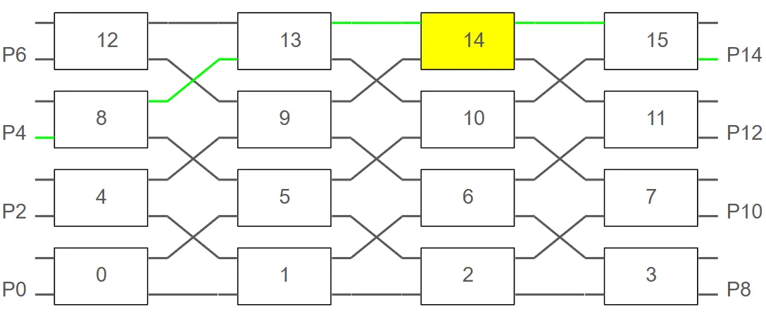
updates = {    ("Unit Cell", 14, "Tunable MZI", 0, "Phase Shifter", 0): {        "model_updates": {"n_complex": index(v_bar)}  # Bar state    }}
# Compute the S-matrix of the full circuit using the updatess_matrix = switch_array.s_matrix(    pf.C_0 / wavelengths, model_kwargs={"updates": updates})
# Plot transmission from input port P4 to output portsfig, ax = pf.plot_s_matrix(    s_matrix, input_ports=["P4"], output_ports=["P8", "P10", "P12", "P14"], y="dB")
# Measures datawavelengths_m = [1.530, 1.535, 1.540, 1.545, 1.547, 1.550, 1.555, 1.560, 1.565]crosstalk_m = [-13.3, -15.8, -19.0, -24.2, -26.6, -22.8, -19.7, -15.9, -13.1]
# Plot the measured crosstalk values vs. wavelengthax[1].plot(wavelengths_m, crosstalk_m, "x-", label="Measurement")ax[1].legend()
Uploading task 'P0@0…'Uploading task 'P1@0…'Uploading task 'P0@0…'Uploading task 'P1@0…'Starting task 'P0@0': https://tidy3d.simulation.cloud/workbench?taskId=fdve-3aefb3fd-4e85-4a5b-84ea-a6c9f645048dStarting task 'P1@0': https://tidy3d.simulation.cloud/workbench?taskId=fdve-6ebde64d-3beb-4fed-9844-36984045bd58Downloading data from 'P0@0'…Starting task 'P1@0': https://tidy3d.simulation.cloud/workbench?taskId=fdve-eea2bd78-a817-48f3-baf7-a6fc6ff7052dStarting task 'P0@0': https://tidy3d.simulation.cloud/workbench?taskId=fdve-89a3f2c0-b836-47ab-a0c7-50183e2fbbdcDownloading data from 'P1@0'…Downloading data from 'P1@0'…Downloading data from 'P0@0'…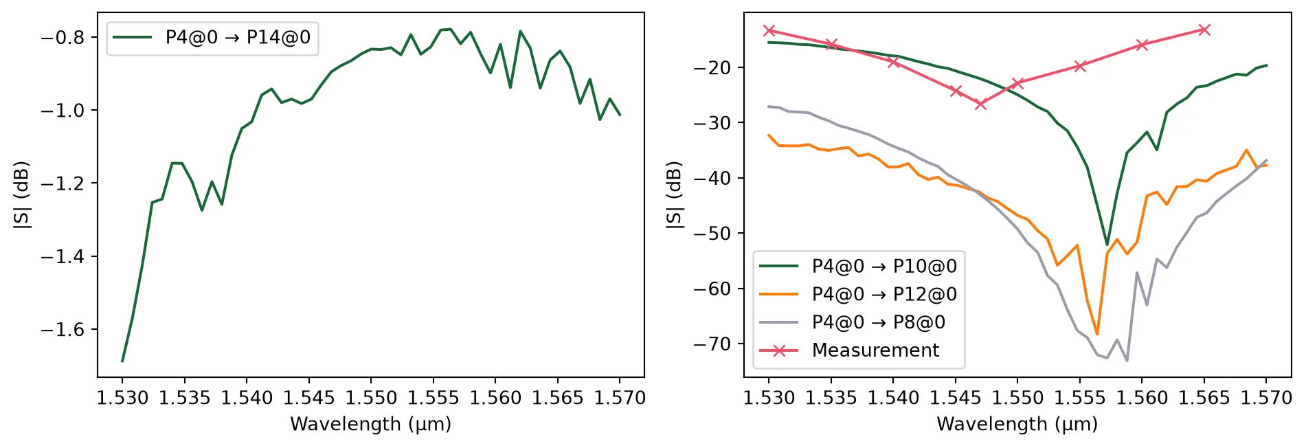
In another configuration, we apply a control voltage to Unit Cell 10 (highlighted in yellow) to drive its MZI into the bar state. As shown in the figure below, this setting redirects the signal from input port P0 to output port P10, following the green-highlighted optical path.
updates = {    ("Unit Cell", 10, "Tunable MZI", 0, "Phase Shifter", 0): {        "model_updates": {"n_complex": index(v_bar)}  # Bar state    }}
# Compute the S-matrix of the full circuit using the updatess_matrix = switch_array.s_matrix(    pf.C_0 / wavelengths, model_kwargs={"updates": updates})
# Plot transmission from P0 to the output portsfig, ax = pf.plot_s_matrix(    s_matrix, input_ports=["P0"], output_ports=["P8", "P10", "P12", "P14"], y="dB")