Components
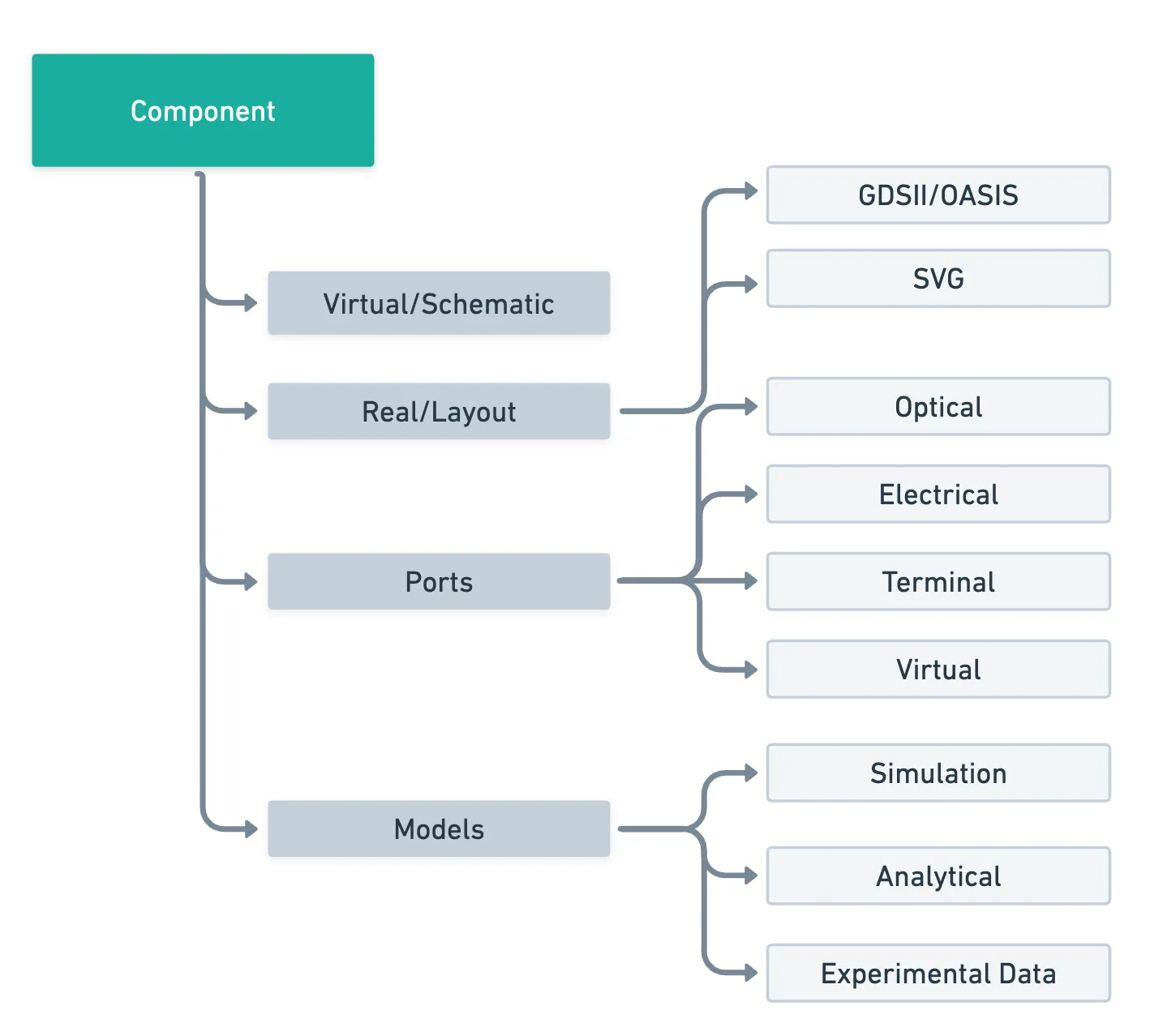
A Component in PhotonForge is like an empty canvas that holds geometric shapes (like rectangles, circles, and polygons), ports (optical or electrical interfaces), models (Tidy3D models, circuit models, waveguide models, data models, and analytical models), and references to other components.
This modular structure simplifies the creation of hierarchical layouts and promotes reuse of subcomponents.
In PhotonForge, all dimensions are in microns, and the layout can be visualized directly within the notebook or exported as GDS files.
import photonforge as pffrom photonforge.live_viewer import LiveViewerimport siepic_forge as siepic
viewer = LiveViewer()
# Set the default technology for this project from the PDK librarypf.config.default_technology = siepic.ebeam()
LiveViewer started at http://127.0.0.1:45867. Call its 'stop()' method to free the port.Drawing a Polygon (Basic Taper Example)
Section titled “Drawing a Polygon (Basic Taper Example)”Let’s define a simple polygon that mimics a waveguide taper—a structure used to transition smoothly from a narrow waveguide to a wider one. Although we’re manually creating this polygon, PhotonForge provides a built-in transition function for generating tapers automatically.
Waveguide tapers are fundamental building blocks in photonic circuits, helping reduce mode-mismatch losses when connecting waveguides of different widths or guiding modes between different photonic components.
c = pf.Component("taper_demo")
# Coordinates of a simple taper-shaped polygon (narrow to wide waveguide)# Taper from width 0.5 µm to 2 µm over 10 µmpolygon = pf.Polygon([(0, -0.25), (0, 0.25), (10, 1.0), (10, -1.0)])c.add((1, 0),polygon)c
Adding Text Labels
Section titled “Adding Text Labels”In PhotonForge, you can conveniently add text labels to your layouts to clearly annotate components or indicate fabrication notes. It’s also straightforward to position elements precisely using offsets. For example, labeling specific structures like waveguides, grating couplers, or alignment marks becomes intuitive and clear.
In this example, we’ll create a simple rectangular waveguide and label it clearly with a text annotation. We’ll also demonstrate using offset positioning.
from photonforge.stencil import as_component
# 1. Create a blank parent componentc = pf.Component("text_offset_demo")
# 2. Create a reusable text component via stencil APItext_comp = as_component(    layer=(10, 0),    stencil="text",    text_string="Waveguide Section",    size=1.0,               # text height in microns)
# 3. Create a simple rectangle component (e.g., a waveguide)rect_comp = pf.Component("waveguide")rect_shape = pf.Rectangle(size=(10, 1))rect_comp.add((1,0),rect_shape)
# 4. Add references of both components into the parentrect_ref   = pf.Reference(rect_comp)text_ref1  = pf.Reference(text_comp)text_ref2  = pf.Reference(text_comp)
c.add_reference(rect_ref)c.add_reference(text_ref1)c.add_reference(text_ref2)
# 5. Position the references with translations and a rotation#    - Center waveguide at origin#    - Label above the waveguide#    - A second label offset and rotated for demonstrationrect_ref.translate((0, 0))text_ref1.translate((0, 1.5))     # 1.5 μm abovetext_ref2.translate((5, 1.5))     # 5 μm to the right, 1.5 μm uptext_ref2.rotate(45)              # rotate label by 45°
# 6. Inspect or exportc.write_gds();fill:%23221f20;font-weight:bold;font-size:0.512190px;}.terminal{fill:none;stroke:%23805080;stroke-width:0.064024;}.dashed{stroke-dasharray:0.320119,0.192071;}.port{fill:none;stroke:%23805080;stroke-width:0.128047;}.virtual-connection{fill:none;stroke:%23907090;stroke-width:0.096036;}.layer_31_0{stroke:%238c78ef;fill:url(%23pat-layer_31_0);fill-opacity:0.492;}.label_31_0{fill:%238c78ef;}.layer_33_0{stroke:%238c78ef;fill:url(%23pat-layer_33_0);fill-opacity:0.492;}.label_33_0{fill:%238c78ef;}.layer_102_0{stroke:%238c78ef;fill:url(%23pat-layer_102_0);fill-opacity:0.492;}.label_102_0{fill:%238c78ef;}.layer_110_0{stroke:%238c78ef;fill:url(%23pat-layer_110_0);fill-opacity:0.492;}.label_110_0{fill:%238c78ef;}.layer_189_0{stroke:%23000000;fill:none;}.label_189_0{fill:%23000000;}.layer_201_0{stroke:%2300ee00;fill:url(%23pat-layer_201_0);fill-opacity:0.492;}.label_201_0{fill:%2300ee00;}.layer_401_0{stroke:%236a8ad2;fill:url(%23pat-layer_401_0);fill-opacity:0.492;}.label_401_0{fill:%236a8ad2;}.layer_202_0{stroke:%23007600;fill:url(%23pat-layer_202_0);fill-opacity:0.492;}.label_202_0{fill:%23007600;}.layer_68_0{stroke:%23008000;fill:url(%23pat-layer_68_0);fill-opacity:0.492;}.label_68_0{fill:%23008000;}.layer_5_0{stroke:%236a8ad2;fill:url(%23pat-layer_5_0);fill-opacity:0.492;}.label_5_0{fill:%236a8ad2;}.layer_998_0{stroke:%23000000;fill:none;}.label_998_0{fill:%23000000;}.layer_312_1{stroke:%2300b8b8;fill:url(%23pat-layer_312_1);fill-opacity:0.492;}.label_312_1{fill:%2300b8b8;}.layer_312_0{stroke:%2300b8b8;fill:url(%23pat-layer_312_0);fill-opacity:0.492;}.label_312_0{fill:%2300b8b8;}.layer_402_0{stroke:%23ff0000;fill:url(%23pat-layer_402_0);fill-opacity:0.492;}.label_402_0{fill:%23ff0000;}.layer_401_4{stroke:%236a8ad2;fill:url(%23pat-layer_401_4);fill-opacity:0.492;}.label_401_4{fill:%236a8ad2;}.layer_389_0{stroke:%23ff00ff;fill:url(%23pat-layer_389_0);fill-opacity:0.492;}.label_389_0{fill:%23ff00ff;}.layer_402_1{stroke:%23ff0000;fill:url(%23pat-layer_402_1);fill-opacity:0.492;}.label_402_1{fill:%23ff0000;}.layer_350_1{stroke:%23697a00;fill:url(%23pat-layer_350_1);fill-opacity:0.492;}.label_350_1{fill:%23697a00;}.layer_401_1{stroke:%236a8ad2;fill:url(%23pat-layer_401_1);fill-opacity:0.492;}.label_401_1{fill:%236a8ad2;}.layer_313_2{stroke:%2301d95b;fill:url(%23pat-layer_313_2);fill-opacity:0.492;}.label_313_2{fill:%2301d95b;}.layer_313_1{stroke:%2301d95b;fill:url(%23pat-layer_313_1);fill-opacity:0.492;}.label_313_1{fill:%2301d95b;}.layer_313_0{stroke:%2301d95b;fill:url(%23pat-layer_313_0);fill-opacity:0.492;}.label_313_0{fill:%2301d95b;}.layer_400_0{stroke:%23a96868;fill:url(%23pat-layer_400_0);fill-opacity:0.492;}.label_400_0{fill:%23a96868;}.layer_312_3{stroke:%2300b8b8;fill:url(%23pat-layer_312_3);fill-opacity:0.492;}.label_312_3{fill:%2300b8b8;}.layer_389_1{stroke:%23ff00ff;fill:url(%23pat-layer_389_1);fill-opacity:0.492;}.label_389_1{fill:%23ff00ff;}.layer_401_3{stroke:%236a8ad2;fill:url(%23pat-layer_401_3);fill-opacity:0.492;}.label_401_3{fill:%236a8ad2;}.layer_403_2{stroke:%23500080;fill:url(%23pat-layer_403_2);fill-opacity:0.492;}.label_403_2{fill:%23500080;}.layer_403_3{stroke:%23500080;fill:url(%23pat-layer_403_3);fill-opacity:0.492;}.label_403_3{fill:%23500080;}.layer_403_1{stroke:%23500080;fill:url(%23pat-layer_403_1);fill-opacity:0.492;}.label_403_1{fill:%23500080;}.layer_403_0{stroke:%23500080;fill:url(%23pat-layer_403_0);fill-opacity:0.492;}.label_403_0{fill:%23500080;}.layer_311_1{stroke:%23ac6c56;fill:url(%23pat-layer_311_1);fill-opacity:0.492;}.label_311_1{fill:%23ac6c56;}.layer_311_0{stroke:%23ac6c56;fill:url(%23pat-layer_311_0);fill-opacity:0.492;}.label_311_0{fill:%23ac6c56;}.layer_301_1{stroke:%23800057;fill:url(%23pat-layer_301_1);fill-opacity:0.492;}.label_301_1{fill:%23800057;}.layer_301_0{stroke:%23800057;fill:url(%23pat-layer_301_0);fill-opacity:0.492;}.label_301_0{fill:%23800057;}.layer_305_1{stroke:%23808080;fill:url(%23pat-layer_305_1);fill-opacity:0.492;}.label_305_1{fill:%23808080;}.layer_305_0{stroke:%23808080;fill:url(%23pat-layer_305_0);fill-opacity:0.492;}.label_305_0{fill:%23808080;}.layer_999_0{stroke:%230000ff;fill:url(%23pat-layer_999_0);fill-opacity:0.492;}.label_999_0{fill:%230000ff;}.layer_81_0{stroke:%23808080;fill:url(%23pat-layer_81_0);fill-opacity:0.492;}.label_81_0{fill:%23808080;}.layer_290_0{stroke:%23a46eda;fill:none;}.label_290_0{fill:%23a46eda;}.layer_205_0{stroke:%2349b203;fill:url(%23pat-layer_205_0);fill-opacity:0.492;}.label_205_0{fill:%2349b203;}.layer_11_0{stroke:%230000ff;fill:url(%23pat-layer_11_0);fill-opacity:0.492;}.label_11_0{fill:%230000ff;}.layer_12_0{stroke:%23a57b00;fill:url(%23pat-layer_12_0);fill-opacity:0.492;}.label_12_0{fill:%23a57b00;}.layer_13_0{stroke:%23800057;fill:url(%23pat-layer_13_0);fill-opacity:0.492;}.label_13_0{fill:%23800057;}.layer_6_0{stroke:%23ff0000;fill:url(%23pat-layer_6_0);fill-opacity:0.492;}.label_6_0{fill:%23ff0000;}.layer_1_10{stroke:%23c96585;fill:url(%23pat-layer_1_10);fill-opacity:0.492;}.label_1_10{fill:%23c96585;}.layer_1_11{stroke:%23800000;fill:url(%23pat-layer_1_11);fill-opacity:0.492;}.label_1_11{fill:%23800000;}.layer_200_0{stroke:%23ff0000;fill:url(%23pat-layer_200_0);fill-opacity:0.492;}.label_200_0{fill:%23ff0000;}.layer_1_0{stroke:%23c96585;fill:url(%23pat-layer_1_0);fill-opacity:0.492;}.label_1_0{fill:%23c96585;}.layer_2_0{stroke:%23a46eda;fill:url(%23pat-layer_2_0);fill-opacity:0.492;}.label_2_0{fill:%23a46eda;}.layer_20_0{stroke:%2353793d;fill:url(%23pat-layer_20_0);fill-opacity:0.492;}.label_20_0{fill:%2353793d;}.layer_22_0{stroke:%23ec7600;fill:url(%23pat-layer_22_0);fill-opacity:0.492;}.label_22_0{fill:%23ec7600;}.layer_24_0{stroke:%2300b8b8;fill:url(%23pat-layer_24_0);fill-opacity:0.492;}.label_24_0{fill:%2300b8b8;}.layer_21_0{stroke:%23736264;fill:url(%23pat-layer_21_0);fill-opacity:0.492;}.label_21_0{fill:%23736264;}.layer_23_0{stroke:%23697a00;fill:url(%23pat-layer_23_0);fill-opacity:0.492;}.label_23_0{fill:%23697a00;}.layer_25_0{stroke:%23008000;fill:url(%23pat-layer_25_0);fill-opacity:0.492;}.label_25_0{fill:%23008000;}.layer_350_0{stroke:%23697a00;fill:url(%23pat-layer_350_0);fill-opacity:0.492;}.label_350_0{fill:%23697a00;}.layer_10_0{stroke:%23000000;fill:none;}.label_10_0{fill:%23000000;}.layer_203_0{stroke:%23008000;fill:url(%23pat-layer_203_0);fill-opacity:0.492;}.label_203_0{fill:%23008000;}.layer_40_0{stroke:%230000ff;fill:url(%23pat-layer_40_0);fill-opacity:0.492;}.label_40_0{fill:%230000ff;}.layer_401_2{stroke:%236a8ad2;fill:url(%23pat-layer_401_2);fill-opacity:0.492;}.label_401_2{fill:%236a8ad2;}.layer_301_2{stroke:%23800057;fill:url(%23pat-layer_301_2);fill-opacity:0.492;}.label_301_2{fill:%23800057;}</style><defs><path id=%22port-symbol%22 class=%22port%22 d=%22M 0,-0.256095 L 0.384142,0 0,0.256095%22 /><path id=%22ref-port-symbol%22 class=%22port%22 style=%22stroke-opacity:0.33;%22 d=%22M 0,-0.192071 C 0.256095,-0.192071 0.256095,0.192071 0,0.192071%22 /><circle id=%22port-bend-symbol%22 style=%22stroke-width:0;stroke:none;fill:%23805080;fill-opacity:1;%22 cx=%220%22 cy=%220%22 r=%220.115243%22 /><circle id=%22connection-symbol%22 style=%22stroke-width:0;stroke:none;fill:%23907090;fill-opacity:1;%22 cx=%220%22 cy=%220%22 r=%220.134450%22 /><pattern id=%22pat-layer_31_0%22 patternUnits=%22userSpaceOnUse%22 width=%220.320119%22 height=%220.320119%22 patternTransform=%22translate(0.244797,0.303270)%22><line x1=%220%22 y1=%220%22 x2=%220.320119%22 y2=%220.320119%22 style=%22stroke:%238c78ef;stroke-width:0.032012%22 /><line x1=%22-0.160059%22 y1=%220.160059%22 x2=%220.160059%22 y2=%220.480178%22 style=%22stroke:%238c78ef;stroke-width:0.032012%22 /><line x1=%220.160059%22 y1=%22-0.160059%22 x2=%220.480178%22 y2=%220.160059%22 style=%22stroke:%238c78ef;stroke-width:0.032012%22 /></pattern><pattern id=%22pat-layer_33_0%22 patternUnits=%22userSpaceOnUse%22 width=%220.320119%22 height=%220.320119%22 patternTransform=%22translate(0.188305,0.033697)%22><line x1=%220%22 y1=%220%22 x2=%220.320119%22 y2=%220.320119%22 style=%22stroke:%238c78ef;stroke-width:0.032012%22 /><line x1=%22-0.160059%22 y1=%220.160059%22 x2=%220.160059%22 y2=%220.480178%22 style=%22stroke:%238c78ef;stroke-width:0.032012%22 /><line x1=%220.160059%22 y1=%22-0.160059%22 x2=%220.480178%22 y2=%220.160059%22 style=%22stroke:%238c78ef;stroke-width:0.032012%22 /></pattern><pattern id=%22pat-layer_102_0%22 patternUnits=%22userSpaceOnUse%22 width=%220.320119%22 height=%220.320119%22 patternTransform=%22translate(0.000000,0.016848)%22><line x1=%220%22 y1=%220%22 x2=%220.320119%22 y2=%220.320119%22 style=%22stroke:%238c78ef;stroke-width:0.032012%22 /><line x1=%22-0.160059%22 y1=%220.160059%22 x2=%220.160059%22 y2=%220.480178%22 style=%22stroke:%238c78ef;stroke-width:0.032012%22 /><line x1=%220.160059%22 y1=%22-0.160059%22 x2=%220.480178%22 y2=%220.160059%22 style=%22stroke:%238c78ef;stroke-width:0.032012%22 /></pattern><pattern id=%22pat-layer_110_0%22 patternUnits=%22userSpaceOnUse%22 width=%220.320119%22 height=%220.320119%22 patternTransform=%22translate(0.094153,0.219028)%22><line x1=%220%22 y1=%220%22 x2=%220.320119%22 y2=%220.320119%22 style=%22stroke:%238c78ef;stroke-width:0.032012%22 /><line x1=%22-0.160059%22 y1=%220.160059%22 x2=%220.160059%22 y2=%220.480178%22 style=%22stroke:%238c78ef;stroke-width:0.032012%22 /><line x1=%220.160059%22 y1=%22-0.160059%22 x2=%220.480178%22 y2=%220.160059%22 style=%22stroke:%238c78ef;stroke-width:0.032012%22 /></pattern><pattern id=%22pat-layer_201_0%22 patternUnits=%22userSpaceOnUse%22 width=%220.320119%22 height=%220.320119%22 patternTransform=%22translate(0.244797,0.117938)%22><circle cx=%220.160059%22 cy=%220.160059%22 r=%220.032012%22 style=%22stroke:none;fill:%2300ee00;fill-opacity:1.0%22 /></pattern><pattern id=%22pat-layer_401_0%22 patternUnits=%22userSpaceOnUse%22 width=%220.192071%22 height=%220.192071%22 patternTransform=%22translate(0.022597,0.030327)%22><line x1=%220%22 y1=%220%22 x2=%220.192071%22 y2=%220.192071%22 style=%22stroke:%236a8ad2;stroke-width:0.032012%22 /><line x1=%22-0.096036%22 y1=%220.096036%22 x2=%220.096036%22 y2=%220.288107%22 style=%22stroke:%236a8ad2;stroke-width:0.032012%22 /><line x1=%220.096036%22 y1=%22-0.096036%22 x2=%220.288107%22 y2=%220.096036%22 style=%22stroke:%236a8ad2;stroke-width:0.032012%22 /><line x1=%220.192071%22 y1=%220%22 x2=%220%22 y2=%220.192071%22 style=%22stroke:%236a8ad2;stroke-width:0.032012%22 /><line x1=%220.288107%22 y1=%220.096036%22 x2=%220.096036%22 y2=%220.288107%22 style=%22stroke:%236a8ad2;stroke-width:0.032012%22 /><line x1=%220.096036%22 y1=%22-0.096036%22 x2=%22-0.096036%22 y2=%220.096036%22 style=%22stroke:%236a8ad2;stroke-width:0.032012%22 /></pattern><pattern id=%22pat-layer_202_0%22 patternUnits=%22userSpaceOnUse%22 width=%220.192071%22 height=%220.192071%22 patternTransform=%22translate(0.033895,0.181962)%22><circle cx=%220.096036%22 cy=%220.096036%22 r=%220.032012%22 style=%22stroke:none;fill:%23007600;fill-opacity:1.0%22 /></pattern><pattern id=%22pat-layer_68_0%22 patternUnits=%22userSpaceOnUse%22 width=%220.320119%22 height=%220.320119%22 patternTransform=%22translate(0.000000,0.117938)%22><circle cx=%220.160059%22 cy=%220.160059%22 r=%220.032012%22 style=%22stroke:none;fill:%23008000;fill-opacity:1.0%22 /></pattern><pattern id=%22pat-layer_5_0%22 patternUnits=%22userSpaceOnUse%22 width=%220.192071%22 height=%220.192071%22 patternTransform=%22translate(0.011298,0.171853)%22><line x1=%220.096036%22 y1=%220%22 x2=%220.096036%22 y2=%220.192071%22 style=%22stroke:%236a8ad2;stroke-width:0.032012%22 /></pattern><pattern id=%22pat-layer_312_1%22 patternUnits=%22userSpaceOnUse%22 width=%220.192071%22 height=%220.192071%22 patternTransform=%22translate(0.045193,0.151635)%22><line x1=%220%22 y1=%220%22 x2=%220.192071%22 y2=%220.192071%22 style=%22stroke:%2300b8b8;stroke-width:0.032012%22 /><line x1=%22-0.096036%22 y1=%220.096036%22 x2=%220.096036%22 y2=%220.288107%22 style=%22stroke:%2300b8b8;stroke-width:0.032012%22 /><line x1=%220.096036%22 y1=%22-0.096036%22 x2=%220.288107%22 y2=%220.096036%22 style=%22stroke:%2300b8b8;stroke-width:0.032012%22 /></pattern><pattern id=%22pat-layer_312_0%22 patternUnits=%22userSpaceOnUse%22 width=%220.320119%22 height=%220.320119%22 patternTransform=%22translate(0.150644,0.202180)%22><line x1=%220.160059%22 y1=%220%22 x2=%220.160059%22 y2=%220.320119%22 style=%22stroke:%2300b8b8;stroke-width:0.032012%22 /></pattern><pattern id=%22pat-layer_402_0%22 patternUnits=%22userSpaceOnUse%22 width=%220.320119%22 height=%220.320119%22 patternTransform=%22translate(0.169475,0.235877)%22><line x1=%220.160059%22 y1=%220%22 x2=%220.160059%22 y2=%220.320119%22 style=%22stroke:%23ff0000;stroke-width:0.032012%22 /><line x1=%220%22 y1=%220.160059%22 x2=%220.320119%22 y2=%220.160059%22 style=%22stroke:%23ff0000;stroke-width:0.032012%22 /></pattern><pattern id=%22pat-layer_401_4%22 patternUnits=%22userSpaceOnUse%22 width=%220.192071%22 height=%220.192071%22 patternTransform=%22translate(0.033895,0.151635)%22><line x1=%220.096036%22 y1=%220%22 x2=%220.096036%22 y2=%220.192071%22 style=%22stroke:%236a8ad2;stroke-width:0.032012%22 /></pattern><pattern id=%22pat-layer_389_0%22 patternUnits=%22userSpaceOnUse%22 width=%220.192071%22 height=%220.192071%22 patternTransform=%22translate(0.033895,0.040436)%22><line x1=%220.096036%22 y1=%220%22 x2=%220.096036%22 y2=%220.192071%22 style=%22stroke:%23ff00ff;stroke-width:0.032012%22 /><line x1=%220%22 y1=%220.096036%22 x2=%220.192071%22 y2=%220.096036%22 style=%22stroke:%23ff00ff;stroke-width:0.032012%22 /></pattern><pattern id=%22pat-layer_402_1%22 patternUnits=%22userSpaceOnUse%22 width=%220.192071%22 height=%220.192071%22 patternTransform=%22translate(0.056492,0.171853)%22><line x1=%220%22 y1=%220%22 x2=%220.192071%22 y2=%220.192071%22 style=%22stroke:%23ff0000;stroke-width:0.032012%22 /><line x1=%22-0.096036%22 y1=%220.096036%22 x2=%220.096036%22 y2=%220.288107%22 style=%22stroke:%23ff0000;stroke-width:0.032012%22 /><line x1=%220.096036%22 y1=%22-0.096036%22 x2=%220.288107%22 y2=%220.096036%22 style=%22stroke:%23ff0000;stroke-width:0.032012%22 /><line x1=%220.192071%22 y1=%220%22 x2=%220%22 y2=%220.192071%22 style=%22stroke:%23ff0000;stroke-width:0.032012%22 /><line x1=%220.288107%22 y1=%220.096036%22 x2=%220.096036%22 y2=%220.288107%22 style=%22stroke:%23ff0000;stroke-width:0.032012%22 /><line x1=%220.096036%22 y1=%22-0.096036%22 x2=%22-0.096036%22 y2=%220.096036%22 style=%22stroke:%23ff0000;stroke-width:0.032012%22 /></pattern><pattern id=%22pat-layer_350_1%22 patternUnits=%22userSpaceOnUse%22 width=%220.192071%22 height=%220.192071%22 patternTransform=%22translate(0.169475,0.151635)%22><circle cx=%220.096036%22 cy=%220.096036%22 r=%220.032012%22 style=%22stroke:none;fill:%23697a00;fill-opacity:1.0%22 /></pattern><pattern id=%22pat-layer_401_1%22 patternUnits=%22userSpaceOnUse%22 width=%220.320119%22 height=%220.320119%22 patternTransform=%22translate(0.282458,0.101090)%22><line x1=%220%22 y1=%220%22 x2=%220.320119%22 y2=%220.320119%22 style=%22stroke:%236a8ad2;stroke-width:0.032012%22 /><line x1=%22-0.160059%22 y1=%220.160059%22 x2=%220.160059%22 y2=%220.480178%22 style=%22stroke:%236a8ad2;stroke-width:0.032012%22 /><line x1=%220.160059%22 y1=%22-0.160059%22 x2=%220.480178%22 y2=%220.160059%22 style=%22stroke:%236a8ad2;stroke-width:0.032012%22 /><line x1=%220.320119%22 y1=%220%22 x2=%220%22 y2=%220.320119%22 style=%22stroke:%236a8ad2;stroke-width:0.032012%22 /><line x1=%220.480178%22 y1=%220.160059%22 x2=%220.160059%22 y2=%220.480178%22 style=%22stroke:%236a8ad2;stroke-width:0.032012%22 /><line x1=%220.160059%22 y1=%22-0.160059%22 x2=%22-0.160059%22 y2=%220.160059%22 style=%22stroke:%236a8ad2;stroke-width:0.032012%22 /></pattern><pattern id=%22pat-layer_313_2%22 patternUnits=%22userSpaceOnUse%22 width=%220.192071%22 height=%220.192071%22 patternTransform=%22translate(0.079088,0.101090)%22><line x1=%220%22 y1=%220%22 x2=%220.192071%22 y2=%220.192071%22 style=%22stroke:%2301d95b;stroke-width:0.032012%22 /><line x1=%22-0.096036%22 y1=%220.096036%22 x2=%220.096036%22 y2=%220.288107%22 style=%22stroke:%2301d95b;stroke-width:0.032012%22 /><line x1=%220.096036%22 y1=%22-0.096036%22 x2=%220.288107%22 y2=%220.096036%22 style=%22stroke:%2301d95b;stroke-width:0.032012%22 /></pattern><pattern id=%22pat-layer_313_1%22 patternUnits=%22userSpaceOnUse%22 width=%220.320119%22 height=%220.320119%22 patternTransform=%22translate(0.207136,0.117938)%22><line x1=%220.160059%22 y1=%220%22 x2=%220.160059%22 y2=%220.320119%22 style=%22stroke:%2301d95b;stroke-width:0.032012%22 /></pattern><pattern id=%22pat-layer_313_0%22 patternUnits=%22userSpaceOnUse%22 width=%220.192071%22 height=%220.192071%22 patternTransform=%22translate(0.169475,0.040436)%22><line x1=%220.096036%22 y1=%220%22 x2=%220.096036%22 y2=%220.192071%22 style=%22stroke:%2301d95b;stroke-width:0.032012%22 /></pattern><pattern id=%22pat-layer_400_0%22 patternUnits=%22userSpaceOnUse%22 width=%220.320119%22 height=%220.320119%22 patternTransform=%22translate(0.225966,0.185332)%22><line x1=%220%22 y1=%220%22 x2=%220.320119%22 y2=%220.320119%22 style=%22stroke:%23a96868;stroke-width:0.032012%22 /><line x1=%22-0.160059%22 y1=%220.160059%22 x2=%220.160059%22 y2=%220.480178%22 style=%22stroke:%23a96868;stroke-width:0.032012%22 /><line x1=%220.160059%22 y1=%22-0.160059%22 x2=%220.480178%22 y2=%220.160059%22 style=%22stroke:%23a96868;stroke-width:0.032012%22 /><line x1=%220.320119%22 y1=%220%22 x2=%220%22 y2=%220.320119%22 style=%22stroke:%23a96868;stroke-width:0.032012%22 /><line x1=%220.480178%22 y1=%220.160059%22 x2=%220.160059%22 y2=%220.480178%22 style=%22stroke:%23a96868;stroke-width:0.032012%22 /><line x1=%220.160059%22 y1=%22-0.160059%22 x2=%22-0.160059%22 y2=%220.160059%22 style=%22stroke:%23a96868;stroke-width:0.032012%22 /></pattern><pattern id=%22pat-layer_312_3%22 patternUnits=%22userSpaceOnUse%22 width=%220.192071%22 height=%220.192071%22 patternTransform=%22translate(0.146878,0.020218)%22><line x1=%220.192071%22 y1=%220%22 x2=%220%22 y2=%220.192071%22 style=%22stroke:%2300b8b8;stroke-width:0.032012%22 /><line x1=%220.288107%22 y1=%220.096036%22 x2=%220.096036%22 y2=%220.288107%22 style=%22stroke:%2300b8b8;stroke-width:0.032012%22 /><line x1=%220.096036%22 y1=%22-0.096036%22 x2=%22-0.096036%22 y2=%220.096036%22 style=%22stroke:%2300b8b8;stroke-width:0.032012%22 /></pattern><pattern id=%22pat-layer_389_1%22 patternUnits=%22userSpaceOnUse%22 width=%220.320119%22 height=%220.320119%22 patternTransform=%22translate(0.301288,0.117938)%22><line x1=%220.160059%22 y1=%220%22 x2=%220.160059%22 y2=%220.320119%22 style=%22stroke:%23ff00ff;stroke-width:0.032012%22 /><line x1=%220%22 y1=%220.160059%22 x2=%220.320119%22 y2=%220.160059%22 style=%22stroke:%23ff00ff;stroke-width:0.032012%22 /></pattern><pattern id=%22pat-layer_401_3%22 patternUnits=%22userSpaceOnUse%22 width=%220.320119%22 height=%220.320119%22 patternTransform=%22translate(0.131814,0.202180)%22><line x1=%220%22 y1=%220.160059%22 x2=%220.320119%22 y2=%220.160059%22 style=%22stroke:%236a8ad2;stroke-width:0.032012%22 /></pattern><pattern id=%22pat-layer_403_2%22 patternUnits=%22userSpaceOnUse%22 width=%220.192071%22 height=%220.192071%22 patternTransform=%22translate(0.090386,0.121308)%22><line x1=%220%22 y1=%220%22 x2=%220.192071%22 y2=%220.192071%22 style=%22stroke:%23500080;stroke-width:0.032012%22 /><line x1=%22-0.096036%22 y1=%220.096036%22 x2=%220.096036%22 y2=%220.288107%22 style=%22stroke:%23500080;stroke-width:0.032012%22 /><line x1=%220.096036%22 y1=%22-0.096036%22 x2=%220.288107%22 y2=%220.096036%22 style=%22stroke:%23500080;stroke-width:0.032012%22 /><line x1=%220.192071%22 y1=%220%22 x2=%220%22 y2=%220.192071%22 style=%22stroke:%23500080;stroke-width:0.032012%22 /><line x1=%220.288107%22 y1=%220.096036%22 x2=%220.096036%22 y2=%220.288107%22 style=%22stroke:%23500080;stroke-width:0.032012%22 /><line x1=%220.096036%22 y1=%22-0.096036%22 x2=%22-0.096036%22 y2=%220.096036%22 style=%22stroke:%23500080;stroke-width:0.032012%22 /></pattern><pattern id=%22pat-layer_403_3%22 patternUnits=%22userSpaceOnUse%22 width=%220.320119%22 height=%220.320119%22 patternTransform=%22translate(0.075322,0.252725)%22><line x1=%220%22 y1=%220%22 x2=%220.320119%22 y2=%220.320119%22 style=%22stroke:%23500080;stroke-width:0.032012%22 /><line x1=%22-0.160059%22 y1=%220.160059%22 x2=%220.160059%22 y2=%220.480178%22 style=%22stroke:%23500080;stroke-width:0.032012%22 /><line x1=%220.160059%22 y1=%22-0.160059%22 x2=%220.480178%22 y2=%220.160059%22 style=%22stroke:%23500080;stroke-width:0.032012%22 /><line x1=%220.320119%22 y1=%220%22 x2=%220%22 y2=%220.320119%22 style=%22stroke:%23500080;stroke-width:0.032012%22 /><line x1=%220.480178%22 y1=%220.160059%22 x2=%220.160059%22 y2=%220.480178%22 style=%22stroke:%23500080;stroke-width:0.032012%22 /><line x1=%220.160059%22 y1=%22-0.160059%22 x2=%22-0.160059%22 y2=%220.160059%22 style=%22stroke:%23500080;stroke-width:0.032012%22 /></pattern><pattern id=%22pat-layer_403_1%22 patternUnits=%22userSpaceOnUse%22 width=%220.320119%22 height=%220.320119%22 patternTransform=%22translate(0.225966,0.151635)%22><line x1=%220.160059%22 y1=%220%22 x2=%220.160059%22 y2=%220.320119%22 style=%22stroke:%23500080;stroke-width:0.032012%22 /><line x1=%220%22 y1=%220.160059%22 x2=%220.320119%22 y2=%220.160059%22 style=%22stroke:%23500080;stroke-width:0.032012%22 /></pattern><pattern id=%22pat-layer_403_0%22 patternUnits=%22userSpaceOnUse%22 width=%220.192071%22 height=%220.192071%22 patternTransform=%22translate(0.180773,0.060654)%22><line x1=%220.096036%22 y1=%220%22 x2=%220.096036%22 y2=%220.192071%22 style=%22stroke:%23500080;stroke-width:0.032012%22 /><line x1=%220%22 y1=%220.096036%22 x2=%220.192071%22 y2=%220.096036%22 style=%22stroke:%23500080;stroke-width:0.032012%22 /></pattern><pattern id=%22pat-layer_311_1%22 patternUnits=%22userSpaceOnUse%22 width=%220.320119%22 height=%220.320119%22 patternTransform=%22translate(0.263627,0.067393)%22><line x1=%220%22 y1=%220%22 x2=%220.320119%22 y2=%220.320119%22 style=%22stroke:%23ac6c56;stroke-width:0.032012%22 /><line x1=%22-0.160059%22 y1=%220.160059%22 x2=%220.160059%22 y2=%220.480178%22 style=%22stroke:%23ac6c56;stroke-width:0.032012%22 /><line x1=%220.160059%22 y1=%22-0.160059%22 x2=%220.480178%22 y2=%220.160059%22 style=%22stroke:%23ac6c56;stroke-width:0.032012%22 /></pattern><pattern id=%22pat-layer_311_0%22 patternUnits=%22userSpaceOnUse%22 width=%220.192071%22 height=%220.192071%22 patternTransform=%22translate(0.011298,0.010109)%22><line x1=%220%22 y1=%220%22 x2=%220.192071%22 y2=%220.192071%22 style=%22stroke:%23ac6c56;stroke-width:0.032012%22 /><line x1=%22-0.096036%22 y1=%220.096036%22 x2=%220.096036%22 y2=%220.288107%22 style=%22stroke:%23ac6c56;stroke-width:0.032012%22 /><line x1=%220.096036%22 y1=%22-0.096036%22 x2=%220.288107%22 y2=%220.096036%22 style=%22stroke:%23ac6c56;stroke-width:0.032012%22 /></pattern><pattern id=%22pat-layer_301_1%22 patternUnits=%22userSpaceOnUse%22 width=%220.320119%22 height=%220.320119%22 patternTransform=%22translate(0.225966,0.134787)%22><line x1=%220%22 y1=%220.160059%22 x2=%220.320119%22 y2=%220.160059%22 style=%22stroke:%23800057;stroke-width:0.032012%22 /></pattern><pattern id=%22pat-layer_301_0%22 patternUnits=%22userSpaceOnUse%22 width=%220.192071%22 height=%220.192071%22 patternTransform=%22translate(0.180773,0.050545)%22><line x1=%220%22 y1=%220.096036%22 x2=%220.192071%22 y2=%220.096036%22 style=%22stroke:%23800057;stroke-width:0.032012%22 /></pattern><pattern id=%22pat-layer_305_1%22 patternUnits=%22userSpaceOnUse%22 width=%220.320119%22 height=%220.320119%22 patternTransform=%22translate(0.112983,0.235877)%22><line x1=%220.160059%22 y1=%220%22 x2=%220.160059%22 y2=%220.320119%22 style=%22stroke:%23808080;stroke-width:0.032012%22 /><line x1=%220%22 y1=%220.160059%22 x2=%220.320119%22 y2=%220.160059%22 style=%22stroke:%23808080;stroke-width:0.032012%22 /></pattern><pattern id=%22pat-layer_305_0%22 patternUnits=%22userSpaceOnUse%22 width=%220.192071%22 height=%220.192071%22 patternTransform=%22translate(0.112983,0.111199)%22><line x1=%220.096036%22 y1=%220%22 x2=%220.096036%22 y2=%220.192071%22 style=%22stroke:%23808080;stroke-width:0.032012%22 /><line x1=%220%22 y1=%220.096036%22 x2=%220.192071%22 y2=%220.096036%22 style=%22stroke:%23808080;stroke-width:0.032012%22 /></pattern><pattern id=%22pat-layer_999_0%22 patternUnits=%22userSpaceOnUse%22 width=%220.192071%22 height=%220.192071%22 patternTransform=%22translate(0.067790,0.070763)%22><line x1=%220.096036%22 y1=%220%22 x2=%220.096036%22 y2=%220.192071%22 style=%22stroke:%230000ff;stroke-width:0.032012%22 /></pattern><pattern id=%22pat-layer_81_0%22 patternUnits=%22userSpaceOnUse%22 width=%220.192071%22 height=%220.192071%22 patternTransform=%22translate(0.067790,0.171853)%22><line x1=%220.096036%22 y1=%220%22 x2=%220.096036%22 y2=%220.192071%22 style=%22stroke:%23808080;stroke-width:0.032012%22 /><line x1=%220%22 y1=%220.096036%22 x2=%220.192071%22 y2=%220.096036%22 style=%22stroke:%23808080;stroke-width:0.032012%22 /></pattern><pattern id=%22pat-layer_205_0%22 patternUnits=%22userSpaceOnUse%22 width=%220.192071%22 height=%220.192071%22 patternTransform=%22translate(0.079088,0.131417)%22><line x1=%220%22 y1=%220%22 x2=%220.192071%22 y2=%220.192071%22 style=%22stroke:%2349b203;stroke-width:0.032012%22 /><line x1=%22-0.096036%22 y1=%220.096036%22 x2=%220.096036%22 y2=%220.288107%22 style=%22stroke:%2349b203;stroke-width:0.032012%22 /><line x1=%220.096036%22 y1=%22-0.096036%22 x2=%220.288107%22 y2=%220.096036%22 style=%22stroke:%2349b203;stroke-width:0.032012%22 /><line x1=%220.192071%22 y1=%220%22 x2=%220%22 y2=%220.192071%22 style=%22stroke:%2349b203;stroke-width:0.032012%22 /><line x1=%220.288107%22 y1=%220.096036%22 x2=%220.096036%22 y2=%220.288107%22 style=%22stroke:%2349b203;stroke-width:0.032012%22 /><line x1=%220.096036%22 y1=%22-0.096036%22 x2=%22-0.096036%22 y2=%220.096036%22 style=%22stroke:%2349b203;stroke-width:0.032012%22 /></pattern><pattern id=%22pat-layer_11_0%22 patternUnits=%22userSpaceOnUse%22 width=%220.192071%22 height=%220.192071%22 patternTransform=%22translate(0.101685,0.070763)%22><line x1=%220.192071%22 y1=%220%22 x2=%220%22 y2=%220.192071%22 style=%22stroke:%230000ff;stroke-width:0.032012%22 /><line x1=%220.288107%22 y1=%220.096036%22 x2=%220.096036%22 y2=%220.288107%22 style=%22stroke:%230000ff;stroke-width:0.032012%22 /><line x1=%220.096036%22 y1=%22-0.096036%22 x2=%22-0.096036%22 y2=%220.096036%22 style=%22stroke:%230000ff;stroke-width:0.032012%22 /></pattern><pattern id=%22pat-layer_12_0%22 patternUnits=%22userSpaceOnUse%22 width=%220.192071%22 height=%220.192071%22 patternTransform=%22translate(0.180773,0.181962)%22><line x1=%220%22 y1=%220%22 x2=%220.192071%22 y2=%220.192071%22 style=%22stroke:%23a57b00;stroke-width:0.032012%22 /><line x1=%22-0.096036%22 y1=%220.096036%22 x2=%220.096036%22 y2=%220.288107%22 style=%22stroke:%23a57b00;stroke-width:0.032012%22 /><line x1=%220.096036%22 y1=%22-0.096036%22 x2=%220.288107%22 y2=%220.096036%22 style=%22stroke:%23a57b00;stroke-width:0.032012%22 /></pattern><pattern id=%22pat-layer_13_0%22 patternUnits=%22userSpaceOnUse%22 width=%220.192071%22 height=%220.192071%22 patternTransform=%22translate(0.067790,0.101090)%22><line x1=%220.192071%22 y1=%220%22 x2=%220%22 y2=%220.192071%22 style=%22stroke:%23800057;stroke-width:0.032012%22 /><line x1=%220.288107%22 y1=%220.096036%22 x2=%220.096036%22 y2=%220.288107%22 style=%22stroke:%23800057;stroke-width:0.032012%22 /><line x1=%220.096036%22 y1=%22-0.096036%22 x2=%22-0.096036%22 y2=%220.096036%22 style=%22stroke:%23800057;stroke-width:0.032012%22 /></pattern><pattern id=%22pat-layer_6_0%22 patternUnits=%22userSpaceOnUse%22 width=%220.320119%22 height=%220.320119%22 patternTransform=%22translate(0.150644,0.151635)%22><line x1=%220%22 y1=%220.160059%22 x2=%220.320119%22 y2=%220.160059%22 style=%22stroke:%23ff0000;stroke-width:0.032012%22 /></pattern><pattern id=%22pat-layer_1_10%22 patternUnits=%22userSpaceOnUse%22 width=%220.192071%22 height=%220.192071%22 patternTransform=%22translate(0.011298,0.030327)%22><line x1=%220%22 y1=%220%22 x2=%220.192071%22 y2=%220.192071%22 style=%22stroke:%23c96585;stroke-width:0.032012%22 /><line x1=%22-0.096036%22 y1=%220.096036%22 x2=%220.096036%22 y2=%220.288107%22 style=%22stroke:%23c96585;stroke-width:0.032012%22 /><line x1=%220.096036%22 y1=%22-0.096036%22 x2=%220.288107%22 y2=%220.096036%22 style=%22stroke:%23c96585;stroke-width:0.032012%22 /><line x1=%220.192071%22 y1=%220%22 x2=%220%22 y2=%220.192071%22 style=%22stroke:%23c96585;stroke-width:0.032012%22 /><line x1=%220.288107%22 y1=%220.096036%22 x2=%220.096036%22 y2=%220.288107%22 style=%22stroke:%23c96585;stroke-width:0.032012%22 /><line x1=%220.096036%22 y1=%22-0.096036%22 x2=%22-0.096036%22 y2=%220.096036%22 style=%22stroke:%23c96585;stroke-width:0.032012%22 /></pattern><pattern id=%22pat-layer_1_11%22 patternUnits=%22userSpaceOnUse%22 width=%220.320119%22 height=%220.320119%22 patternTransform=%22translate(0.263627,0.101090)%22><line x1=%220.160059%22 y1=%220%22 x2=%220.160059%22 y2=%220.320119%22 style=%22stroke:%23800000;stroke-width:0.032012%22 /><line x1=%220%22 y1=%220.160059%22 x2=%220.320119%22 y2=%220.160059%22 style=%22stroke:%23800000;stroke-width:0.032012%22 /></pattern><pattern id=%22pat-layer_200_0%22 patternUnits=%22userSpaceOnUse%22 width=%220.320119%22 height=%220.320119%22 patternTransform=%22translate(0.112983,0.252725)%22><line x1=%220%22 y1=%220%22 x2=%220.320119%22 y2=%220.320119%22 style=%22stroke:%23ff0000;stroke-width:0.032012%22 /><line x1=%22-0.160059%22 y1=%220.160059%22 x2=%220.160059%22 y2=%220.480178%22 style=%22stroke:%23ff0000;stroke-width:0.032012%22 /><line x1=%220.160059%22 y1=%22-0.160059%22 x2=%220.480178%22 y2=%220.160059%22 style=%22stroke:%23ff0000;stroke-width:0.032012%22 /><line x1=%220.320119%22 y1=%220%22 x2=%220%22 y2=%220.320119%22 style=%22stroke:%23ff0000;stroke-width:0.032012%22 /><line x1=%220.480178%22 y1=%220.160059%22 x2=%220.160059%22 y2=%220.480178%22 style=%22stroke:%23ff0000;stroke-width:0.032012%22 /><line x1=%220.160059%22 y1=%22-0.160059%22 x2=%22-0.160059%22 y2=%220.160059%22 style=%22stroke:%23ff0000;stroke-width:0.032012%22 /></pattern><pattern id=%22pat-layer_1_0%22 patternUnits=%22userSpaceOnUse%22 width=%220.192071%22 height=%220.192071%22 patternTransform=%22translate(0.079088,0.111199)%22><line x1=%220.192071%22 y1=%220%22 x2=%220%22 y2=%220.192071%22 style=%22stroke:%23c96585;stroke-width:0.032012%22 /><line x1=%220.288107%22 y1=%220.096036%22 x2=%220.096036%22 y2=%220.288107%22 style=%22stroke:%23c96585;stroke-width:0.032012%22 /><line x1=%220.096036%22 y1=%22-0.096036%22 x2=%22-0.096036%22 y2=%220.096036%22 style=%22stroke:%23c96585;stroke-width:0.032012%22 /></pattern><pattern id=%22pat-layer_2_0%22 patternUnits=%22userSpaceOnUse%22 width=%220.320119%22 height=%220.320119%22 patternTransform=%22translate(0.263627,0.050545)%22><line x1=%220%22 y1=%220%22 x2=%220.320119%22 y2=%220.320119%22 style=%22stroke:%23a46eda;stroke-width:0.032012%22 /><line x1=%22-0.160059%22 y1=%220.160059%22 x2=%220.160059%22 y2=%220.480178%22 style=%22stroke:%23a46eda;stroke-width:0.032012%22 /><line x1=%220.160059%22 y1=%22-0.160059%22 x2=%220.480178%22 y2=%220.160059%22 style=%22stroke:%23a46eda;stroke-width:0.032012%22 /></pattern><pattern id=%22pat-layer_20_0%22 patternUnits=%22userSpaceOnUse%22 width=%220.320119%22 height=%220.320119%22 patternTransform=%22translate(0.075322,0.185332)%22><line x1=%220%22 y1=%220.160059%22 x2=%220.320119%22 y2=%220.160059%22 style=%22stroke:%2353793d;stroke-width:0.032012%22 /></pattern><pattern id=%22pat-layer_22_0%22 patternUnits=%22userSpaceOnUse%22 width=%220.320119%22 height=%220.320119%22 patternTransform=%22translate(0.018831,0.235877)%22><line x1=%220%22 y1=%220%22 x2=%220.320119%22 y2=%220.320119%22 style=%22stroke:%23ec7600;stroke-width:0.032012%22 /><line x1=%22-0.160059%22 y1=%220.160059%22 x2=%220.160059%22 y2=%220.480178%22 style=%22stroke:%23ec7600;stroke-width:0.032012%22 /><line x1=%220.160059%22 y1=%22-0.160059%22 x2=%220.480178%22 y2=%220.160059%22 style=%22stroke:%23ec7600;stroke-width:0.032012%22 /><line x1=%220.320119%22 y1=%220%22 x2=%220%22 y2=%220.320119%22 style=%22stroke:%23ec7600;stroke-width:0.032012%22 /><line x1=%220.480178%22 y1=%220.160059%22 x2=%220.160059%22 y2=%220.480178%22 style=%22stroke:%23ec7600;stroke-width:0.032012%22 /><line x1=%220.160059%22 y1=%22-0.160059%22 x2=%22-0.160059%22 y2=%220.160059%22 style=%22stroke:%23ec7600;stroke-width:0.032012%22 /></pattern><pattern id=%22pat-layer_24_0%22 patternUnits=%22userSpaceOnUse%22 width=%220.320119%22 height=%220.320119%22 patternTransform=%22translate(0.282458,0.286422)%22><line x1=%220.160059%22 y1=%220%22 x2=%220.160059%22 y2=%220.320119%22 style=%22stroke:%2300b8b8;stroke-width:0.032012%22 /><line x1=%220%22 y1=%220.160059%22 x2=%220.320119%22 y2=%220.160059%22 style=%22stroke:%2300b8b8;stroke-width:0.032012%22 /></pattern><pattern id=%22pat-layer_21_0%22 patternUnits=%22userSpaceOnUse%22 width=%220.192071%22 height=%220.192071%22 patternTransform=%22translate(0.124281,0.030327)%22><line x1=%220%22 y1=%220.096036%22 x2=%220.192071%22 y2=%220.096036%22 style=%22stroke:%23736264;stroke-width:0.032012%22 /></pattern><pattern id=%22pat-layer_23_0%22 patternUnits=%22userSpaceOnUse%22 width=%220.192071%22 height=%220.192071%22 patternTransform=%22translate(0.090386,0.060654)%22><line x1=%220%22 y1=%220%22 x2=%220.192071%22 y2=%220.192071%22 style=%22stroke:%23697a00;stroke-width:0.032012%22 /><line x1=%22-0.096036%22 y1=%220.096036%22 x2=%220.096036%22 y2=%220.288107%22 style=%22stroke:%23697a00;stroke-width:0.032012%22 /><line x1=%220.096036%22 y1=%22-0.096036%22 x2=%220.288107%22 y2=%220.096036%22 style=%22stroke:%23697a00;stroke-width:0.032012%22 /><line x1=%220.192071%22 y1=%220%22 x2=%220%22 y2=%220.192071%22 style=%22stroke:%23697a00;stroke-width:0.032012%22 /><line x1=%220.288107%22 y1=%220.096036%22 x2=%220.096036%22 y2=%220.288107%22 style=%22stroke:%23697a00;stroke-width:0.032012%22 /><line x1=%220.096036%22 y1=%22-0.096036%22 x2=%22-0.096036%22 y2=%220.096036%22 style=%22stroke:%23697a00;stroke-width:0.032012%22 /></pattern><pattern id=%22pat-layer_25_0%22 patternUnits=%22userSpaceOnUse%22 width=%220.192071%22 height=%220.192071%22 patternTransform=%22translate(0.056492,0.090981)%22><line x1=%220.096036%22 y1=%220%22 x2=%220.096036%22 y2=%220.192071%22 style=%22stroke:%23008000;stroke-width:0.032012%22 /><line x1=%220%22 y1=%220.096036%22 x2=%220.192071%22 y2=%220.096036%22 style=%22stroke:%23008000;stroke-width:0.032012%22 /></pattern><pattern id=%22pat-layer_350_0%22 patternUnits=%22userSpaceOnUse%22 width=%220.320119%22 height=%220.320119%22 patternTransform=%22translate(0.037661,0.202180)%22><line x1=%220.320119%22 y1=%220%22 x2=%220%22 y2=%220.320119%22 style=%22stroke:%23697a00;stroke-width:0.032012%22 /><line x1=%220.480178%22 y1=%220.160059%22 x2=%220.160059%22 y2=%220.480178%22 style=%22stroke:%23697a00;stroke-width:0.032012%22 /><line x1=%220.160059%22 y1=%22-0.160059%22 x2=%22-0.160059%22 y2=%220.160059%22 style=%22stroke:%23697a00;stroke-width:0.032012%22 /></pattern><pattern id=%22pat-layer_203_0%22 patternUnits=%22userSpaceOnUse%22 width=%220.320119%22 height=%220.320119%22 patternTransform=%22translate(0.188305,0.168483)%22><line x1=%220.320119%22 y1=%220%22 x2=%220%22 y2=%220.320119%22 style=%22stroke:%23008000;stroke-width:0.032012%22 /><line x1=%220.480178%22 y1=%220.160059%22 x2=%220.160059%22 y2=%220.480178%22 style=%22stroke:%23008000;stroke-width:0.032012%22 /><line x1=%220.160059%22 y1=%22-0.160059%22 x2=%22-0.160059%22 y2=%220.160059%22 style=%22stroke:%23008000;stroke-width:0.032012%22 /></pattern><pattern id=%22pat-layer_40_0%22 patternUnits=%22userSpaceOnUse%22 width=%220.320119%22 height=%220.320119%22 patternTransform=%22translate(0.150644,0.050545)%22><circle cx=%220.160059%22 cy=%220.160059%22 r=%220.032012%22 style=%22stroke:none;fill:%230000ff;fill-opacity:1.0%22 /></pattern><pattern id=%22pat-layer_401_2%22 patternUnits=%22userSpaceOnUse%22 width=%220.192071%22 height=%220.192071%22 patternTransform=%22translate(0.124281,0.090981)%22><line x1=%220%22 y1=%220.096036%22 x2=%220.192071%22 y2=%220.096036%22 style=%22stroke:%236a8ad2;stroke-width:0.032012%22 /></pattern><pattern id=%22pat-layer_301_2%22 patternUnits=%22userSpaceOnUse%22 width=%220.192071%22 height=%220.192071%22 patternTransform=%22translate(0.090386,0.111199)%22><line x1=%220.096036%22 y1=%220%22 x2=%220.096036%22 y2=%220.192071%22 style=%22stroke:%23800057;stroke-width:0.032012%22 /></pattern><g id=%22C1%22 data-name=%22waveguide%22><rect class=%22layer_1_0%22 x=%22-5.000000%22 y=%22-0.500000%22 width=%2210.000000%22 height=%221.000000%22 /></g><g id=%22C2%22 data-name=%22as_component__ONFPE32274CNJXKI77JUQFOQQ7ATXVYXHHNA2SOXMEYXB4GYAXPA%22><path class=%22layer_10_0%22 d=%22M 0.000000,0.200000 0.113000,0.200000 0.300000,0.388000 0.488000,0.200000 0.600000,0.200000 0.600000,0.850000 0.500000,0.850000 0.500000,0.400000 0.450000,0.400000 0.300000,0.550000 0.150000,0.400000 0.100000,0.400000 0.100000,0.850000 0.000000,0.850000 z%22 /><path class=%22layer_10_0%22 d=%22M 0.890000,0.300000 0.840000,0.300000 0.840000,0.375000 1.040000,0.375000 1.040000,0.300000 0.990000,0.300000 0.990000,0.200000 1.140000,0.200000 1.140000,0.600000 1.090000,0.650000 0.790000,0.650000 0.740000,0.600000 0.740000,0.550000 1.040000,0.550000 1.040000,0.475000 0.815000,0.475000 0.740000,0.400000 0.740000,0.275000 0.815000,0.200000 0.890000,0.200000 z%22 /><path class=%22layer_10_0%22 d=%22M 1.630000,0.600000 1.630000,0.650000 1.530000,0.650000 1.480000,0.300000 1.430000,0.300000 1.380000,0.650000 1.280000,0.650000 1.280000,0.600000 1.343000,0.200000 1.568000,0.200000 z%22 /><path class=%22layer_10_0%22 d=%22M 2.145000,0.300000 1.870000,0.300000 1.870000,0.550000 2.070000,0.550000 2.070000,0.475000 1.945000,0.475000 1.945000,0.375000 2.095000,0.375000 2.170000,0.450000 2.170000,0.575000 2.095000,0.650000 1.845000,0.650000 1.770000,0.575000 1.770000,0.275000 1.845000,0.200000 2.145000,0.200000 z%22 /><path class=%22layer_10_0%22 d=%22M 2.710000,0.650000 2.423000,0.650000 2.310000,0.538000 2.310000,0.313000 2.423000,0.200000 2.610000,0.200000 2.610000,0.100000 2.410000,0.100000 2.410000,0.000000 2.635000,0.000000 2.710000,0.075000 2.710000,0.375000 2.610000,0.375000 2.610000,0.300000 2.460000,0.300000 2.410000,0.350000 2.410000,0.500000 2.460000,0.550000 2.610000,0.550000 2.610000,0.475000 2.710000,0.475000 z%22 /><path class=%22layer_10_0%22 d=%22M 3.200000,0.200000 3.200000,0.650000 3.100000,0.650000 3.100000,0.350000 3.050000,0.300000 3.000000,0.300000 2.950000,0.350000 2.950000,0.650000 2.850000,0.650000 2.850000,0.313000 2.963000,0.200000 3.063000,0.200000 3.100000,0.238000 3.138000,0.200000 z%22 /><path class=%22layer_10_0%22 d=%22M 3.340000,0.550000 3.340000,0.200000 3.440000,0.200000 3.440000,0.550000 z%22 /><path class=%22layer_10_0%22 d=%22M 3.340000,0.750000 3.340000,0.650000 3.440000,0.650000 3.440000,0.750000 z%22 /><path class=%22layer_10_0%22 d=%22M 3.980000,0.375000 3.880000,0.375000 3.880000,0.300000 3.730000,0.300000 3.680000,0.350000 3.680000,0.475000 3.730000,0.525000 3.880000,0.525000 3.880000,0.475000 3.980000,0.475000 3.980000,0.850000 3.880000,0.850000 3.880000,0.625000 3.693000,0.625000 3.580000,0.513000 3.580000,0.313000 3.693000,0.200000 3.980000,0.200000 z%22 /><path class=%22layer_10_0%22 d=%22M 4.495000,0.300000 4.220000,0.300000 4.220000,0.550000 4.420000,0.550000 4.420000,0.475000 4.295000,0.475000 4.295000,0.375000 4.445000,0.375000 4.520000,0.450000 4.520000,0.575000 4.445000,0.650000 4.195000,0.650000 4.120000,0.575000 4.120000,0.275000 4.195000,0.200000 4.495000,0.200000 z%22 /><path class=%22layer_10_0%22 d=%22M 5.670000,0.738000 5.558000,0.850000 5.333000,0.850000 5.220000,0.738000 5.220000,0.600000 5.345000,0.475000 5.520000,0.475000 5.570000,0.425000 5.570000,0.350000 5.520000,0.300000 5.370000,0.300000 5.308000,0.363000 5.220000,0.363000 5.220000,0.313000 5.333000,0.200000 5.558000,0.200000 5.670000,0.313000 5.670000,0.450000 5.545000,0.575000 5.370000,0.575000 5.320000,0.625000 5.320000,0.700000 5.370000,0.750000 5.520000,0.750000 5.583000,0.688000 5.670000,0.688000 z%22 /><path class=%22layer_10_0%22 d=%22M 6.185000,0.300000 5.910000,0.300000 5.910000,0.550000 6.110000,0.550000 6.110000,0.475000 5.985000,0.475000 5.985000,0.375000 6.135000,0.375000 6.210000,0.450000 6.210000,0.575000 6.135000,0.650000 5.885000,0.650000 5.810000,0.575000 5.810000,0.275000 5.885000,0.200000 6.185000,0.200000 z%22 /><path class=%22layer_10_0%22 d=%22M 6.750000,0.363000 6.663000,0.363000 6.600000,0.300000 6.500000,0.300000 6.450000,0.350000 6.450000,0.500000 6.500000,0.550000 6.600000,0.550000 6.663000,0.488000 6.750000,0.488000 6.750000,0.538000 6.638000,0.650000 6.463000,0.650000 6.350000,0.538000 6.350000,0.313000 6.463000,0.200000 6.638000,0.200000 6.750000,0.313000 z%22 /><path class=%22layer_10_0%22 d=%22M 7.190000,0.300000 7.090000,0.300000 7.090000,0.600000 7.190000,0.600000 7.190000,0.700000 7.090000,0.700000 7.090000,0.850000 6.990000,0.850000 6.990000,0.700000 6.890000,0.700000 6.890000,0.600000 6.990000,0.600000 6.990000,0.275000 7.065000,0.200000 7.190000,0.200000 z%22 /><path class=%22layer_10_0%22 d=%22M 7.330000,0.550000 7.330000,0.200000 7.430000,0.200000 7.430000,0.550000 z%22 /><path class=%22layer_10_0%22 d=%22M 7.330000,0.750000 7.330000,0.650000 7.430000,0.650000 7.430000,0.750000 z%22 /><path class=%22layer_10_0%22 d=%22M 7.870000,0.200000 7.970000,0.300000 7.970000,0.538000 7.858000,0.650000 7.683000,0.650000 7.570000,0.538000 7.570000,0.300000 7.670000,0.200000 7.720000,0.200000 7.720000,0.300000 7.670000,0.350000 7.670000,0.500000 7.720000,0.550000 7.820000,0.550000 7.870000,0.500000 7.870000,0.350000 7.820000,0.300000 7.820000,0.200000 z%22 /><path class=%22layer_10_0%22 d=%22M 8.110000,0.650000 8.110000,0.200000 8.210000,0.200000 8.210000,0.500000 8.260000,0.550000 8.310000,0.550000 8.360000,0.500000 8.360000,0.200000 8.460000,0.200000 8.460000,0.538000 8.348000,0.650000 8.248000,0.650000 8.210000,0.613000 8.173000,0.650000 z%22 /></g></defs><g transform=%22scale(1 -1)%22><g id=%22C0%22 data-name=%22text_offset_demo%22><use transform=%22translate(0.000000 0.000000)%22 href=%22%23C1%22 /><use transform=%22translate(0.000000 1.500000)%22 href=%22%23C2%22 /><use transform=%22translate(2.474870 4.596190) rotate(45.000000)%22 href=%22%23C2%22 /></g></g></svg>)
%22><rect x=%22-30.00%22 y=%22-30.00%22 width=%2260.00%22 height=%2260.00%22 fill=%22%23f4f5f7%22 stroke=%22%23232530%22 stroke-width=%221%22/><use href=%22%23g-wg%22 transform=%22translate(-30.00 -30.00) scale(1.2)%22/></g><text x=%2240.00%22 y=%22431.80%22 font-size=%229%22 fill=%22%23232530%22 font-weight=%22400%22 text-anchor=%22middle%22 dominant-baseline=%22hanging%22 stroke=%22%23ffffff%22 stroke-width=%223.15%22 stroke-linejoin=%22round%22 paint-order=%22stroke%22>waveguide_1</text><g transform=%22matrix(1 -0 0 1 40.000 200.000)%22><rect x=%22-30.00%22 y=%22-30.00%22 width=%2260.00%22 height=%2260.00%22 fill=%22%23f4f5f7%22 stroke=%22%23232530%22 stroke-width=%221%22/></g><text x=%2240.00%22 y=%22200.00%22 font-size=%226.5%22 fill=%22%23232530%22 font-weight=%22400%22 text-anchor=%22middle%22 dominant-baseline=%22middle%22 stroke=%22%23ffffff%22 stroke-width=%222.27%22 stroke-linejoin=%22round%22 paint-order=%22stroke%22>as_component</text><text x=%2240.00%22 y=%22231.80%22 font-size=%229%22 fill=%22%23232530%22 font-weight=%22400%22 text-anchor=%22middle%22 dominant-baseline=%22hanging%22 stroke=%22%23ffffff%22 stroke-width=%223.15%22 stroke-linejoin=%22round%22 paint-order=%22stroke%22>as_component_1</text><g transform=%22matrix(0.707107 -0.707107 0.707107 0.707107 40.000 40.000)%22><rect x=%22-30.00%22 y=%22-30.00%22 width=%2260.00%22 height=%2260.00%22 fill=%22%23f4f5f7%22 stroke=%22%23232530%22 stroke-width=%221%22/></g><text x=%2240.00%22 y=%2240.00%22 font-size=%226.5%22 fill=%22%23232530%22 font-weight=%22400%22 text-anchor=%22middle%22 dominant-baseline=%22middle%22 stroke=%22%23ffffff%22 stroke-width=%222.27%22 stroke-linejoin=%22round%22 paint-order=%22stroke%22>as_component</text><text x=%2240.00%22 y=%2271.80%22 font-size=%229%22 fill=%22%23232530%22 font-weight=%22400%22 text-anchor=%22middle%22 dominant-baseline=%22hanging%22 stroke=%22%23ffffff%22 stroke-width=%223.15%22 stroke-linejoin=%22round%22 paint-order=%22stroke%22>as_component_2</text><g fill=%22none%22 stroke-width=%222%22></g></svg>)
Offsetting a Polygon
Section titled “Offsetting a Polygon”PhotonForge can offset any polygon to create enlarged or contracted copies. This is useful for generating buffer regions, cladding outlines, or general shape expansions.
Below, we define a simple taper-like polygon and offset it by 2 µm.
# 1. Create a blank componentc = pf.Component("offset_demo")
# 2. Define a polygon shapepoly = pf.Polygon([(0, 0), (5, 1), (10, 1), (10, -1), (5, -1)])
# 3. Add the original polygon on layer (1,0)c.add((1, 0), poly)
# 4. Offset the polygon by 2 µmoffset_shapes = pf.offset(poly, distance=2.0)
# 5. Add the offset shapes on layer (2,0)for shape in offset_shapes:    c.add((2, 0), shape)
# 6. View the resultc
Boolean Difference Between Shapes
You can perform boolean operations between polygons. Here, we subtract the original polygon from its offset copy to get the “ring” or margin region.
# 1. Compute the difference: offset minus originalmargin_shapes = pf.boolean(offset_shapes, poly, operation="-")
# 2. Add the resulting margin on layer (3,0)for shape in margin_shapes:    c.add((3, 0), shape)
# 3. View the resultc
Extracting Boolean Results into a Separate Component
For modularity, you may want to isolate the boolean result into its own component. This makes it easy to export or manipulate that region independently.
# 1. Create a new component for the margin regionmargin_comp = pf.Component("margin_only")
# 2. Add each margin polygon on layer (3,0)for shape in margin_shapes:    margin_comp.add((3, 0), shape)
# 3. View the isolated margin componentmargin_comp
References
Section titled “References”Connecting Ports
Section titled “Connecting Ports”Components can have “ports” that let you snap Component References together, just like LEGO bricks. Here we:
- Create three straight segments via the
straightparametric function. - Position them with simple translations and rotations.
- Connect them by matching port names.
Each straight segment provides two ports, named P0 (left side) and P1 (right side).
from photonforge.parametric import straight
# 1. Create a blank componentc = pf.Component("port_connection_demo")
# 2. Create three straight segmentswg1 = pf.Reference(straight(port_spec="TE_1550_500", length=2.0))c.add_reference(wg1)
wg2 = pf.Reference(straight(port_spec="TE_1550_500", length=3.0))wg2.translate((0, 10))wg2.rotate(10)c.add_reference(wg2)
wg3 = pf.Reference(straight(port_spec="TE_1550_500", length=5.0))wg3.translate((0, 20))wg3.rotate(15)c.add_reference(wg3)
c;fill:%23221f20;font-weight:bold;font-size:0.928580px;}.terminal{fill:none;stroke:%23805080;stroke-width:0.116073;}.dashed{stroke-dasharray:0.580363,0.348218;}.port{fill:none;stroke:%23805080;stroke-width:0.232145;}.virtual-connection{fill:none;stroke:%23907090;stroke-width:0.174109;}.layer_31_0{stroke:%238c78ef;fill:url(%23pat-layer_31_0);fill-opacity:0.492;}.label_31_0{fill:%238c78ef;}.layer_33_0{stroke:%238c78ef;fill:url(%23pat-layer_33_0);fill-opacity:0.492;}.label_33_0{fill:%238c78ef;}.layer_102_0{stroke:%238c78ef;fill:url(%23pat-layer_102_0);fill-opacity:0.492;}.label_102_0{fill:%238c78ef;}.layer_110_0{stroke:%238c78ef;fill:url(%23pat-layer_110_0);fill-opacity:0.492;}.label_110_0{fill:%238c78ef;}.layer_189_0{stroke:%23000000;fill:none;}.label_189_0{fill:%23000000;}.layer_201_0{stroke:%2300ee00;fill:url(%23pat-layer_201_0);fill-opacity:0.492;}.label_201_0{fill:%2300ee00;}.layer_401_0{stroke:%236a8ad2;fill:url(%23pat-layer_401_0);fill-opacity:0.492;}.label_401_0{fill:%236a8ad2;}.layer_202_0{stroke:%23007600;fill:url(%23pat-layer_202_0);fill-opacity:0.492;}.label_202_0{fill:%23007600;}.layer_68_0{stroke:%23008000;fill:url(%23pat-layer_68_0);fill-opacity:0.492;}.label_68_0{fill:%23008000;}.layer_5_0{stroke:%236a8ad2;fill:url(%23pat-layer_5_0);fill-opacity:0.492;}.label_5_0{fill:%236a8ad2;}.layer_998_0{stroke:%23000000;fill:none;}.label_998_0{fill:%23000000;}.layer_312_1{stroke:%2300b8b8;fill:url(%23pat-layer_312_1);fill-opacity:0.492;}.label_312_1{fill:%2300b8b8;}.layer_312_0{stroke:%2300b8b8;fill:url(%23pat-layer_312_0);fill-opacity:0.492;}.label_312_0{fill:%2300b8b8;}.layer_402_0{stroke:%23ff0000;fill:url(%23pat-layer_402_0);fill-opacity:0.492;}.label_402_0{fill:%23ff0000;}.layer_401_4{stroke:%236a8ad2;fill:url(%23pat-layer_401_4);fill-opacity:0.492;}.label_401_4{fill:%236a8ad2;}.layer_389_0{stroke:%23ff00ff;fill:url(%23pat-layer_389_0);fill-opacity:0.492;}.label_389_0{fill:%23ff00ff;}.layer_402_1{stroke:%23ff0000;fill:url(%23pat-layer_402_1);fill-opacity:0.492;}.label_402_1{fill:%23ff0000;}.layer_350_1{stroke:%23697a00;fill:url(%23pat-layer_350_1);fill-opacity:0.492;}.label_350_1{fill:%23697a00;}.layer_401_1{stroke:%236a8ad2;fill:url(%23pat-layer_401_1);fill-opacity:0.492;}.label_401_1{fill:%236a8ad2;}.layer_313_2{stroke:%2301d95b;fill:url(%23pat-layer_313_2);fill-opacity:0.492;}.label_313_2{fill:%2301d95b;}.layer_313_1{stroke:%2301d95b;fill:url(%23pat-layer_313_1);fill-opacity:0.492;}.label_313_1{fill:%2301d95b;}.layer_313_0{stroke:%2301d95b;fill:url(%23pat-layer_313_0);fill-opacity:0.492;}.label_313_0{fill:%2301d95b;}.layer_400_0{stroke:%23a96868;fill:url(%23pat-layer_400_0);fill-opacity:0.492;}.label_400_0{fill:%23a96868;}.layer_312_3{stroke:%2300b8b8;fill:url(%23pat-layer_312_3);fill-opacity:0.492;}.label_312_3{fill:%2300b8b8;}.layer_389_1{stroke:%23ff00ff;fill:url(%23pat-layer_389_1);fill-opacity:0.492;}.label_389_1{fill:%23ff00ff;}.layer_401_3{stroke:%236a8ad2;fill:url(%23pat-layer_401_3);fill-opacity:0.492;}.label_401_3{fill:%236a8ad2;}.layer_403_2{stroke:%23500080;fill:url(%23pat-layer_403_2);fill-opacity:0.492;}.label_403_2{fill:%23500080;}.layer_403_3{stroke:%23500080;fill:url(%23pat-layer_403_3);fill-opacity:0.492;}.label_403_3{fill:%23500080;}.layer_403_1{stroke:%23500080;fill:url(%23pat-layer_403_1);fill-opacity:0.492;}.label_403_1{fill:%23500080;}.layer_403_0{stroke:%23500080;fill:url(%23pat-layer_403_0);fill-opacity:0.492;}.label_403_0{fill:%23500080;}.layer_311_1{stroke:%23ac6c56;fill:url(%23pat-layer_311_1);fill-opacity:0.492;}.label_311_1{fill:%23ac6c56;}.layer_311_0{stroke:%23ac6c56;fill:url(%23pat-layer_311_0);fill-opacity:0.492;}.label_311_0{fill:%23ac6c56;}.layer_301_1{stroke:%23800057;fill:url(%23pat-layer_301_1);fill-opacity:0.492;}.label_301_1{fill:%23800057;}.layer_301_0{stroke:%23800057;fill:url(%23pat-layer_301_0);fill-opacity:0.492;}.label_301_0{fill:%23800057;}.layer_305_1{stroke:%23808080;fill:url(%23pat-layer_305_1);fill-opacity:0.492;}.label_305_1{fill:%23808080;}.layer_305_0{stroke:%23808080;fill:url(%23pat-layer_305_0);fill-opacity:0.492;}.label_305_0{fill:%23808080;}.layer_999_0{stroke:%230000ff;fill:url(%23pat-layer_999_0);fill-opacity:0.492;}.label_999_0{fill:%230000ff;}.layer_81_0{stroke:%23808080;fill:url(%23pat-layer_81_0);fill-opacity:0.492;}.label_81_0{fill:%23808080;}.layer_290_0{stroke:%23a46eda;fill:none;}.label_290_0{fill:%23a46eda;}.layer_205_0{stroke:%2349b203;fill:url(%23pat-layer_205_0);fill-opacity:0.492;}.label_205_0{fill:%2349b203;}.layer_11_0{stroke:%230000ff;fill:url(%23pat-layer_11_0);fill-opacity:0.492;}.label_11_0{fill:%230000ff;}.layer_12_0{stroke:%23a57b00;fill:url(%23pat-layer_12_0);fill-opacity:0.492;}.label_12_0{fill:%23a57b00;}.layer_13_0{stroke:%23800057;fill:url(%23pat-layer_13_0);fill-opacity:0.492;}.label_13_0{fill:%23800057;}.layer_6_0{stroke:%23ff0000;fill:url(%23pat-layer_6_0);fill-opacity:0.492;}.label_6_0{fill:%23ff0000;}.layer_1_10{stroke:%23c96585;fill:url(%23pat-layer_1_10);fill-opacity:0.492;}.label_1_10{fill:%23c96585;}.layer_1_11{stroke:%23800000;fill:url(%23pat-layer_1_11);fill-opacity:0.492;}.label_1_11{fill:%23800000;}.layer_200_0{stroke:%23ff0000;fill:url(%23pat-layer_200_0);fill-opacity:0.492;}.label_200_0{fill:%23ff0000;}.layer_1_0{stroke:%23c96585;fill:url(%23pat-layer_1_0);fill-opacity:0.492;}.label_1_0{fill:%23c96585;}.layer_2_0{stroke:%23a46eda;fill:url(%23pat-layer_2_0);fill-opacity:0.492;}.label_2_0{fill:%23a46eda;}.layer_20_0{stroke:%2353793d;fill:url(%23pat-layer_20_0);fill-opacity:0.492;}.label_20_0{fill:%2353793d;}.layer_22_0{stroke:%23ec7600;fill:url(%23pat-layer_22_0);fill-opacity:0.492;}.label_22_0{fill:%23ec7600;}.layer_24_0{stroke:%2300b8b8;fill:url(%23pat-layer_24_0);fill-opacity:0.492;}.label_24_0{fill:%2300b8b8;}.layer_21_0{stroke:%23736264;fill:url(%23pat-layer_21_0);fill-opacity:0.492;}.label_21_0{fill:%23736264;}.layer_23_0{stroke:%23697a00;fill:url(%23pat-layer_23_0);fill-opacity:0.492;}.label_23_0{fill:%23697a00;}.layer_25_0{stroke:%23008000;fill:url(%23pat-layer_25_0);fill-opacity:0.492;}.label_25_0{fill:%23008000;}.layer_350_0{stroke:%23697a00;fill:url(%23pat-layer_350_0);fill-opacity:0.492;}.label_350_0{fill:%23697a00;}.layer_10_0{stroke:%23000000;fill:none;}.label_10_0{fill:%23000000;}.layer_203_0{stroke:%23008000;fill:url(%23pat-layer_203_0);fill-opacity:0.492;}.label_203_0{fill:%23008000;}.layer_40_0{stroke:%230000ff;fill:url(%23pat-layer_40_0);fill-opacity:0.492;}.label_40_0{fill:%230000ff;}.layer_401_2{stroke:%236a8ad2;fill:url(%23pat-layer_401_2);fill-opacity:0.492;}.label_401_2{fill:%236a8ad2;}.layer_301_2{stroke:%23800057;fill:url(%23pat-layer_301_2);fill-opacity:0.492;}.label_301_2{fill:%23800057;}</style><defs><path id=%22port-symbol%22 class=%22port%22 d=%22M 0,-0.464290 L 0.696435,0 0,0.464290%22 /><path id=%22ref-port-symbol%22 class=%22port%22 style=%22stroke-opacity:0.33;%22 d=%22M 0,-0.348218 C 0.464290,-0.348218 0.464290,0.348218 0,0.348218%22 /><circle id=%22port-bend-symbol%22 style=%22stroke-width:0;stroke:none;fill:%23805080;fill-opacity:1;%22 cx=%220%22 cy=%220%22 r=%220.208931%22 /><circle id=%22connection-symbol%22 style=%22stroke-width:0;stroke:none;fill:%23907090;fill-opacity:1;%22 cx=%220%22 cy=%220%22 r=%220.243752%22 /><pattern id=%22pat-layer_31_0%22 patternUnits=%22userSpaceOnUse%22 width=%220.580363%22 height=%220.580363%22 patternTransform=%22translate(0.443807,0.549817)%22><line x1=%220%22 y1=%220%22 x2=%220.580363%22 y2=%220.580363%22 style=%22stroke:%238c78ef;stroke-width:0.058036%22 /><line x1=%22-0.290181%22 y1=%220.290181%22 x2=%220.290181%22 y2=%220.870544%22 style=%22stroke:%238c78ef;stroke-width:0.058036%22 /><line x1=%220.290181%22 y1=%22-0.290181%22 x2=%220.870544%22 y2=%220.290181%22 style=%22stroke:%238c78ef;stroke-width:0.058036%22 /></pattern><pattern id=%22pat-layer_33_0%22 patternUnits=%22userSpaceOnUse%22 width=%220.580363%22 height=%220.580363%22 patternTransform=%22translate(0.341390,0.061091)%22><line x1=%220%22 y1=%220%22 x2=%220.580363%22 y2=%220.580363%22 style=%22stroke:%238c78ef;stroke-width:0.058036%22 /><line x1=%22-0.290181%22 y1=%220.290181%22 x2=%220.290181%22 y2=%220.870544%22 style=%22stroke:%238c78ef;stroke-width:0.058036%22 /><line x1=%220.290181%22 y1=%22-0.290181%22 x2=%220.870544%22 y2=%220.290181%22 style=%22stroke:%238c78ef;stroke-width:0.058036%22 /></pattern><pattern id=%22pat-layer_102_0%22 patternUnits=%22userSpaceOnUse%22 width=%220.580363%22 height=%220.580363%22 patternTransform=%22translate(0.000000,0.030545)%22><line x1=%220%22 y1=%220%22 x2=%220.580363%22 y2=%220.580363%22 style=%22stroke:%238c78ef;stroke-width:0.058036%22 /><line x1=%22-0.290181%22 y1=%220.290181%22 x2=%220.290181%22 y2=%220.870544%22 style=%22stroke:%238c78ef;stroke-width:0.058036%22 /><line x1=%220.290181%22 y1=%22-0.290181%22 x2=%220.870544%22 y2=%220.290181%22 style=%22stroke:%238c78ef;stroke-width:0.058036%22 /></pattern><pattern id=%22pat-layer_110_0%22 patternUnits=%22userSpaceOnUse%22 width=%220.580363%22 height=%220.580363%22 patternTransform=%22translate(0.170695,0.397090)%22><line x1=%220%22 y1=%220%22 x2=%220.580363%22 y2=%220.580363%22 style=%22stroke:%238c78ef;stroke-width:0.058036%22 /><line x1=%22-0.290181%22 y1=%220.290181%22 x2=%220.290181%22 y2=%220.870544%22 style=%22stroke:%238c78ef;stroke-width:0.058036%22 /><line x1=%220.290181%22 y1=%22-0.290181%22 x2=%220.870544%22 y2=%220.290181%22 style=%22stroke:%238c78ef;stroke-width:0.058036%22 /></pattern><pattern id=%22pat-layer_201_0%22 patternUnits=%22userSpaceOnUse%22 width=%220.580363%22 height=%220.580363%22 patternTransform=%22translate(0.443807,0.213818)%22><circle cx=%220.290181%22 cy=%220.290181%22 r=%220.058036%22 style=%22stroke:none;fill:%2300ee00;fill-opacity:1.0%22 /></pattern><pattern id=%22pat-layer_401_0%22 patternUnits=%22userSpaceOnUse%22 width=%220.348218%22 height=%220.348218%22 patternTransform=%22translate(0.040967,0.054982)%22><line x1=%220%22 y1=%220%22 x2=%220.348218%22 y2=%220.348218%22 style=%22stroke:%236a8ad2;stroke-width:0.058036%22 /><line x1=%22-0.174109%22 y1=%220.174109%22 x2=%220.174109%22 y2=%220.522326%22 style=%22stroke:%236a8ad2;stroke-width:0.058036%22 /><line x1=%220.174109%22 y1=%22-0.174109%22 x2=%220.522326%22 y2=%220.174109%22 style=%22stroke:%236a8ad2;stroke-width:0.058036%22 /><line x1=%220.348218%22 y1=%220%22 x2=%220%22 y2=%220.348218%22 style=%22stroke:%236a8ad2;stroke-width:0.058036%22 /><line x1=%220.522326%22 y1=%220.174109%22 x2=%220.174109%22 y2=%220.522326%22 style=%22stroke:%236a8ad2;stroke-width:0.058036%22 /><line x1=%220.174109%22 y1=%22-0.174109%22 x2=%22-0.174109%22 y2=%220.174109%22 style=%22stroke:%236a8ad2;stroke-width:0.058036%22 /></pattern><pattern id=%22pat-layer_202_0%22 patternUnits=%22userSpaceOnUse%22 width=%220.348218%22 height=%220.348218%22 patternTransform=%22translate(0.061450,0.329890)%22><circle cx=%220.174109%22 cy=%220.174109%22 r=%220.058036%22 style=%22stroke:none;fill:%23007600;fill-opacity:1.0%22 /></pattern><pattern id=%22pat-layer_68_0%22 patternUnits=%22userSpaceOnUse%22 width=%220.580363%22 height=%220.580363%22 patternTransform=%22translate(0.000000,0.213818)%22><circle cx=%220.290181%22 cy=%220.290181%22 r=%220.058036%22 style=%22stroke:none;fill:%23008000;fill-opacity:1.0%22 /></pattern><pattern id=%22pat-layer_5_0%22 patternUnits=%22userSpaceOnUse%22 width=%220.348218%22 height=%220.348218%22 patternTransform=%22translate(0.020483,0.311563)%22><line x1=%220.174109%22 y1=%220%22 x2=%220.174109%22 y2=%220.348218%22 style=%22stroke:%236a8ad2;stroke-width:0.058036%22 /></pattern><pattern id=%22pat-layer_312_1%22 patternUnits=%22userSpaceOnUse%22 width=%220.348218%22 height=%220.348218%22 patternTransform=%22translate(0.081934,0.274909)%22><line x1=%220%22 y1=%220%22 x2=%220.348218%22 y2=%220.348218%22 style=%22stroke:%2300b8b8;stroke-width:0.058036%22 /><line x1=%22-0.174109%22 y1=%220.174109%22 x2=%220.174109%22 y2=%220.522326%22 style=%22stroke:%2300b8b8;stroke-width:0.058036%22 /><line x1=%220.174109%22 y1=%22-0.174109%22 x2=%220.522326%22 y2=%220.174109%22 style=%22stroke:%2300b8b8;stroke-width:0.058036%22 /></pattern><pattern id=%22pat-layer_312_0%22 patternUnits=%22userSpaceOnUse%22 width=%220.580363%22 height=%220.580363%22 patternTransform=%22translate(0.273112,0.366545)%22><line x1=%220.290181%22 y1=%220%22 x2=%220.290181%22 y2=%220.580363%22 style=%22stroke:%2300b8b8;stroke-width:0.058036%22 /></pattern><pattern id=%22pat-layer_402_0%22 patternUnits=%22userSpaceOnUse%22 width=%220.580363%22 height=%220.580363%22 patternTransform=%22translate(0.307251,0.427636)%22><line x1=%220.290181%22 y1=%220%22 x2=%220.290181%22 y2=%220.580363%22 style=%22stroke:%23ff0000;stroke-width:0.058036%22 /><line x1=%220%22 y1=%220.290181%22 x2=%220.580363%22 y2=%220.290181%22 style=%22stroke:%23ff0000;stroke-width:0.058036%22 /></pattern><pattern id=%22pat-layer_401_4%22 patternUnits=%22userSpaceOnUse%22 width=%220.348218%22 height=%220.348218%22 patternTransform=%22translate(0.061450,0.274909)%22><line x1=%220.174109%22 y1=%220%22 x2=%220.174109%22 y2=%220.348218%22 style=%22stroke:%236a8ad2;stroke-width:0.058036%22 /></pattern><pattern id=%22pat-layer_389_0%22 patternUnits=%22userSpaceOnUse%22 width=%220.348218%22 height=%220.348218%22 patternTransform=%22translate(0.061450,0.073309)%22><line x1=%220.174109%22 y1=%220%22 x2=%220.174109%22 y2=%220.348218%22 style=%22stroke:%23ff00ff;stroke-width:0.058036%22 /><line x1=%220%22 y1=%220.174109%22 x2=%220.348218%22 y2=%220.174109%22 style=%22stroke:%23ff00ff;stroke-width:0.058036%22 /></pattern><pattern id=%22pat-layer_402_1%22 patternUnits=%22userSpaceOnUse%22 width=%220.348218%22 height=%220.348218%22 patternTransform=%22translate(0.102417,0.311563)%22><line x1=%220%22 y1=%220%22 x2=%220.348218%22 y2=%220.348218%22 style=%22stroke:%23ff0000;stroke-width:0.058036%22 /><line x1=%22-0.174109%22 y1=%220.174109%22 x2=%220.174109%22 y2=%220.522326%22 style=%22stroke:%23ff0000;stroke-width:0.058036%22 /><line x1=%220.174109%22 y1=%22-0.174109%22 x2=%220.522326%22 y2=%220.174109%22 style=%22stroke:%23ff0000;stroke-width:0.058036%22 /><line x1=%220.348218%22 y1=%220%22 x2=%220%22 y2=%220.348218%22 style=%22stroke:%23ff0000;stroke-width:0.058036%22 /><line x1=%220.522326%22 y1=%220.174109%22 x2=%220.174109%22 y2=%220.522326%22 style=%22stroke:%23ff0000;stroke-width:0.058036%22 /><line x1=%220.174109%22 y1=%22-0.174109%22 x2=%22-0.174109%22 y2=%220.174109%22 style=%22stroke:%23ff0000;stroke-width:0.058036%22 /></pattern><pattern id=%22pat-layer_350_1%22 patternUnits=%22userSpaceOnUse%22 width=%220.348218%22 height=%220.348218%22 patternTransform=%22translate(0.307251,0.274909)%22><circle cx=%220.174109%22 cy=%220.174109%22 r=%220.058036%22 style=%22stroke:none;fill:%23697a00;fill-opacity:1.0%22 /></pattern><pattern id=%22pat-layer_401_1%22 patternUnits=%22userSpaceOnUse%22 width=%220.580363%22 height=%220.580363%22 patternTransform=%22translate(0.512085,0.183272)%22><line x1=%220%22 y1=%220%22 x2=%220.580363%22 y2=%220.580363%22 style=%22stroke:%236a8ad2;stroke-width:0.058036%22 /><line x1=%22-0.290181%22 y1=%220.290181%22 x2=%220.290181%22 y2=%220.870544%22 style=%22stroke:%236a8ad2;stroke-width:0.058036%22 /><line x1=%220.290181%22 y1=%22-0.290181%22 x2=%220.870544%22 y2=%220.290181%22 style=%22stroke:%236a8ad2;stroke-width:0.058036%22 /><line x1=%220.580363%22 y1=%220%22 x2=%220%22 y2=%220.580363%22 style=%22stroke:%236a8ad2;stroke-width:0.058036%22 /><line x1=%220.870544%22 y1=%220.290181%22 x2=%220.290181%22 y2=%220.870544%22 style=%22stroke:%236a8ad2;stroke-width:0.058036%22 /><line x1=%220.290181%22 y1=%22-0.290181%22 x2=%22-0.290181%22 y2=%220.290181%22 style=%22stroke:%236a8ad2;stroke-width:0.058036%22 /></pattern><pattern id=%22pat-layer_313_2%22 patternUnits=%22userSpaceOnUse%22 width=%220.348218%22 height=%220.348218%22 patternTransform=%22translate(0.143384,0.183272)%22><line x1=%220%22 y1=%220%22 x2=%220.348218%22 y2=%220.348218%22 style=%22stroke:%2301d95b;stroke-width:0.058036%22 /><line x1=%22-0.174109%22 y1=%220.174109%22 x2=%220.174109%22 y2=%220.522326%22 style=%22stroke:%2301d95b;stroke-width:0.058036%22 /><line x1=%220.174109%22 y1=%22-0.174109%22 x2=%220.522326%22 y2=%220.174109%22 style=%22stroke:%2301d95b;stroke-width:0.058036%22 /></pattern><pattern id=%22pat-layer_313_1%22 patternUnits=%22userSpaceOnUse%22 width=%220.580363%22 height=%220.580363%22 patternTransform=%22translate(0.375529,0.213818)%22><line x1=%220.290181%22 y1=%220%22 x2=%220.290181%22 y2=%220.580363%22 style=%22stroke:%2301d95b;stroke-width:0.058036%22 /></pattern><pattern id=%22pat-layer_313_0%22 patternUnits=%22userSpaceOnUse%22 width=%220.348218%22 height=%220.348218%22 patternTransform=%22translate(0.307251,0.073309)%22><line x1=%220.174109%22 y1=%220%22 x2=%220.174109%22 y2=%220.348218%22 style=%22stroke:%2301d95b;stroke-width:0.058036%22 /></pattern><pattern id=%22pat-layer_400_0%22 patternUnits=%22userSpaceOnUse%22 width=%220.580363%22 height=%220.580363%22 patternTransform=%22translate(0.409668,0.335999)%22><line x1=%220%22 y1=%220%22 x2=%220.580363%22 y2=%220.580363%22 style=%22stroke:%23a96868;stroke-width:0.058036%22 /><line x1=%22-0.290181%22 y1=%220.290181%22 x2=%220.290181%22 y2=%220.870544%22 style=%22stroke:%23a96868;stroke-width:0.058036%22 /><line x1=%220.290181%22 y1=%22-0.290181%22 x2=%220.870544%22 y2=%220.290181%22 style=%22stroke:%23a96868;stroke-width:0.058036%22 /><line x1=%220.580363%22 y1=%220%22 x2=%220%22 y2=%220.580363%22 style=%22stroke:%23a96868;stroke-width:0.058036%22 /><line x1=%220.870544%22 y1=%220.290181%22 x2=%220.290181%22 y2=%220.870544%22 style=%22stroke:%23a96868;stroke-width:0.058036%22 /><line x1=%220.290181%22 y1=%22-0.290181%22 x2=%22-0.290181%22 y2=%220.290181%22 style=%22stroke:%23a96868;stroke-width:0.058036%22 /></pattern><pattern id=%22pat-layer_312_3%22 patternUnits=%22userSpaceOnUse%22 width=%220.348218%22 height=%220.348218%22 patternTransform=%22translate(0.266284,0.036654)%22><line x1=%220.348218%22 y1=%220%22 x2=%220%22 y2=%220.348218%22 style=%22stroke:%2300b8b8;stroke-width:0.058036%22 /><line x1=%220.522326%22 y1=%220.174109%22 x2=%220.174109%22 y2=%220.522326%22 style=%22stroke:%2300b8b8;stroke-width:0.058036%22 /><line x1=%220.174109%22 y1=%22-0.174109%22 x2=%22-0.174109%22 y2=%220.174109%22 style=%22stroke:%2300b8b8;stroke-width:0.058036%22 /></pattern><pattern id=%22pat-layer_389_1%22 patternUnits=%22userSpaceOnUse%22 width=%220.580363%22 height=%220.580363%22 patternTransform=%22translate(0.546224,0.213818)%22><line x1=%220.290181%22 y1=%220%22 x2=%220.290181%22 y2=%220.580363%22 style=%22stroke:%23ff00ff;stroke-width:0.058036%22 /><line x1=%220%22 y1=%220.290181%22 x2=%220.580363%22 y2=%220.290181%22 style=%22stroke:%23ff00ff;stroke-width:0.058036%22 /></pattern><pattern id=%22pat-layer_401_3%22 patternUnits=%22userSpaceOnUse%22 width=%220.580363%22 height=%220.580363%22 patternTransform=%22translate(0.238973,0.366545)%22><line x1=%220%22 y1=%220.290181%22 x2=%220.580363%22 y2=%220.290181%22 style=%22stroke:%236a8ad2;stroke-width:0.058036%22 /></pattern><pattern id=%22pat-layer_403_2%22 patternUnits=%22userSpaceOnUse%22 width=%220.348218%22 height=%220.348218%22 patternTransform=%22translate(0.163867,0.219927)%22><line x1=%220%22 y1=%220%22 x2=%220.348218%22 y2=%220.348218%22 style=%22stroke:%23500080;stroke-width:0.058036%22 /><line x1=%22-0.174109%22 y1=%220.174109%22 x2=%220.174109%22 y2=%220.522326%22 style=%22stroke:%23500080;stroke-width:0.058036%22 /><line x1=%220.174109%22 y1=%22-0.174109%22 x2=%220.522326%22 y2=%220.174109%22 style=%22stroke:%23500080;stroke-width:0.058036%22 /><line x1=%220.348218%22 y1=%220%22 x2=%220%22 y2=%220.348218%22 style=%22stroke:%23500080;stroke-width:0.058036%22 /><line x1=%220.522326%22 y1=%220.174109%22 x2=%220.174109%22 y2=%220.522326%22 style=%22stroke:%23500080;stroke-width:0.058036%22 /><line x1=%220.174109%22 y1=%22-0.174109%22 x2=%22-0.174109%22 y2=%220.174109%22 style=%22stroke:%23500080;stroke-width:0.058036%22 /></pattern><pattern id=%22pat-layer_403_3%22 patternUnits=%22userSpaceOnUse%22 width=%220.580363%22 height=%220.580363%22 patternTransform=%22translate(0.136556,0.458181)%22><line x1=%220%22 y1=%220%22 x2=%220.580363%22 y2=%220.580363%22 style=%22stroke:%23500080;stroke-width:0.058036%22 /><line x1=%22-0.290181%22 y1=%220.290181%22 x2=%220.290181%22 y2=%220.870544%22 style=%22stroke:%23500080;stroke-width:0.058036%22 /><line x1=%220.290181%22 y1=%22-0.290181%22 x2=%220.870544%22 y2=%220.290181%22 style=%22stroke:%23500080;stroke-width:0.058036%22 /><line x1=%220.580363%22 y1=%220%22 x2=%220%22 y2=%220.580363%22 style=%22stroke:%23500080;stroke-width:0.058036%22 /><line x1=%220.870544%22 y1=%220.290181%22 x2=%220.290181%22 y2=%220.870544%22 style=%22stroke:%23500080;stroke-width:0.058036%22 /><line x1=%220.290181%22 y1=%22-0.290181%22 x2=%22-0.290181%22 y2=%220.290181%22 style=%22stroke:%23500080;stroke-width:0.058036%22 /></pattern><pattern id=%22pat-layer_403_1%22 patternUnits=%22userSpaceOnUse%22 width=%220.580363%22 height=%220.580363%22 patternTransform=%22translate(0.409668,0.274909)%22><line x1=%220.290181%22 y1=%220%22 x2=%220.290181%22 y2=%220.580363%22 style=%22stroke:%23500080;stroke-width:0.058036%22 /><line x1=%220%22 y1=%220.290181%22 x2=%220.580363%22 y2=%220.290181%22 style=%22stroke:%23500080;stroke-width:0.058036%22 /></pattern><pattern id=%22pat-layer_403_0%22 patternUnits=%22userSpaceOnUse%22 width=%220.348218%22 height=%220.348218%22 patternTransform=%22translate(0.327734,0.109963)%22><line x1=%220.174109%22 y1=%220%22 x2=%220.174109%22 y2=%220.348218%22 style=%22stroke:%23500080;stroke-width:0.058036%22 /><line x1=%220%22 y1=%220.174109%22 x2=%220.348218%22 y2=%220.174109%22 style=%22stroke:%23500080;stroke-width:0.058036%22 /></pattern><pattern id=%22pat-layer_311_1%22 patternUnits=%22userSpaceOnUse%22 width=%220.580363%22 height=%220.580363%22 patternTransform=%22translate(0.477946,0.122182)%22><line x1=%220%22 y1=%220%22 x2=%220.580363%22 y2=%220.580363%22 style=%22stroke:%23ac6c56;stroke-width:0.058036%22 /><line x1=%22-0.290181%22 y1=%220.290181%22 x2=%220.290181%22 y2=%220.870544%22 style=%22stroke:%23ac6c56;stroke-width:0.058036%22 /><line x1=%220.290181%22 y1=%22-0.290181%22 x2=%220.870544%22 y2=%220.290181%22 style=%22stroke:%23ac6c56;stroke-width:0.058036%22 /></pattern><pattern id=%22pat-layer_311_0%22 patternUnits=%22userSpaceOnUse%22 width=%220.348218%22 height=%220.348218%22 patternTransform=%22translate(0.020483,0.018327)%22><line x1=%220%22 y1=%220%22 x2=%220.348218%22 y2=%220.348218%22 style=%22stroke:%23ac6c56;stroke-width:0.058036%22 /><line x1=%22-0.174109%22 y1=%220.174109%22 x2=%220.174109%22 y2=%220.522326%22 style=%22stroke:%23ac6c56;stroke-width:0.058036%22 /><line x1=%220.174109%22 y1=%22-0.174109%22 x2=%220.522326%22 y2=%220.174109%22 style=%22stroke:%23ac6c56;stroke-width:0.058036%22 /></pattern><pattern id=%22pat-layer_301_1%22 patternUnits=%22userSpaceOnUse%22 width=%220.580363%22 height=%220.580363%22 patternTransform=%22translate(0.409668,0.244363)%22><line x1=%220%22 y1=%220.290181%22 x2=%220.580363%22 y2=%220.290181%22 style=%22stroke:%23800057;stroke-width:0.058036%22 /></pattern><pattern id=%22pat-layer_301_0%22 patternUnits=%22userSpaceOnUse%22 width=%220.348218%22 height=%220.348218%22 patternTransform=%22translate(0.327734,0.091636)%22><line x1=%220%22 y1=%220.174109%22 x2=%220.348218%22 y2=%220.174109%22 style=%22stroke:%23800057;stroke-width:0.058036%22 /></pattern><pattern id=%22pat-layer_305_1%22 patternUnits=%22userSpaceOnUse%22 width=%220.580363%22 height=%220.580363%22 patternTransform=%22translate(0.204834,0.427636)%22><line x1=%220.290181%22 y1=%220%22 x2=%220.290181%22 y2=%220.580363%22 style=%22stroke:%23808080;stroke-width:0.058036%22 /><line x1=%220%22 y1=%220.290181%22 x2=%220.580363%22 y2=%220.290181%22 style=%22stroke:%23808080;stroke-width:0.058036%22 /></pattern><pattern id=%22pat-layer_305_0%22 patternUnits=%22userSpaceOnUse%22 width=%220.348218%22 height=%220.348218%22 patternTransform=%22translate(0.204834,0.201600)%22><line x1=%220.174109%22 y1=%220%22 x2=%220.174109%22 y2=%220.348218%22 style=%22stroke:%23808080;stroke-width:0.058036%22 /><line x1=%220%22 y1=%220.174109%22 x2=%220.348218%22 y2=%220.174109%22 style=%22stroke:%23808080;stroke-width:0.058036%22 /></pattern><pattern id=%22pat-layer_999_0%22 patternUnits=%22userSpaceOnUse%22 width=%220.348218%22 height=%220.348218%22 patternTransform=%22translate(0.122900,0.128291)%22><line x1=%220.174109%22 y1=%220%22 x2=%220.174109%22 y2=%220.348218%22 style=%22stroke:%230000ff;stroke-width:0.058036%22 /></pattern><pattern id=%22pat-layer_81_0%22 patternUnits=%22userSpaceOnUse%22 width=%220.348218%22 height=%220.348218%22 patternTransform=%22translate(0.122900,0.311563)%22><line x1=%220.174109%22 y1=%220%22 x2=%220.174109%22 y2=%220.348218%22 style=%22stroke:%23808080;stroke-width:0.058036%22 /><line x1=%220%22 y1=%220.174109%22 x2=%220.348218%22 y2=%220.174109%22 style=%22stroke:%23808080;stroke-width:0.058036%22 /></pattern><pattern id=%22pat-layer_205_0%22 patternUnits=%22userSpaceOnUse%22 width=%220.348218%22 height=%220.348218%22 patternTransform=%22translate(0.143384,0.238254)%22><line x1=%220%22 y1=%220%22 x2=%220.348218%22 y2=%220.348218%22 style=%22stroke:%2349b203;stroke-width:0.058036%22 /><line x1=%22-0.174109%22 y1=%220.174109%22 x2=%220.174109%22 y2=%220.522326%22 style=%22stroke:%2349b203;stroke-width:0.058036%22 /><line x1=%220.174109%22 y1=%22-0.174109%22 x2=%220.522326%22 y2=%220.174109%22 style=%22stroke:%2349b203;stroke-width:0.058036%22 /><line x1=%220.348218%22 y1=%220%22 x2=%220%22 y2=%220.348218%22 style=%22stroke:%2349b203;stroke-width:0.058036%22 /><line x1=%220.522326%22 y1=%220.174109%22 x2=%220.174109%22 y2=%220.522326%22 style=%22stroke:%2349b203;stroke-width:0.058036%22 /><line x1=%220.174109%22 y1=%22-0.174109%22 x2=%22-0.174109%22 y2=%220.174109%22 style=%22stroke:%2349b203;stroke-width:0.058036%22 /></pattern><pattern id=%22pat-layer_11_0%22 patternUnits=%22userSpaceOnUse%22 width=%220.348218%22 height=%220.348218%22 patternTransform=%22translate(0.184351,0.128291)%22><line x1=%220.348218%22 y1=%220%22 x2=%220%22 y2=%220.348218%22 style=%22stroke:%230000ff;stroke-width:0.058036%22 /><line x1=%220.522326%22 y1=%220.174109%22 x2=%220.174109%22 y2=%220.522326%22 style=%22stroke:%230000ff;stroke-width:0.058036%22 /><line x1=%220.174109%22 y1=%22-0.174109%22 x2=%22-0.174109%22 y2=%220.174109%22 style=%22stroke:%230000ff;stroke-width:0.058036%22 /></pattern><pattern id=%22pat-layer_12_0%22 patternUnits=%22userSpaceOnUse%22 width=%220.348218%22 height=%220.348218%22 patternTransform=%22translate(0.327734,0.329890)%22><line x1=%220%22 y1=%220%22 x2=%220.348218%22 y2=%220.348218%22 style=%22stroke:%23a57b00;stroke-width:0.058036%22 /><line x1=%22-0.174109%22 y1=%220.174109%22 x2=%220.174109%22 y2=%220.522326%22 style=%22stroke:%23a57b00;stroke-width:0.058036%22 /><line x1=%220.174109%22 y1=%22-0.174109%22 x2=%220.522326%22 y2=%220.174109%22 style=%22stroke:%23a57b00;stroke-width:0.058036%22 /></pattern><pattern id=%22pat-layer_13_0%22 patternUnits=%22userSpaceOnUse%22 width=%220.348218%22 height=%220.348218%22 patternTransform=%22translate(0.122900,0.183272)%22><line x1=%220.348218%22 y1=%220%22 x2=%220%22 y2=%220.348218%22 style=%22stroke:%23800057;stroke-width:0.058036%22 /><line x1=%220.522326%22 y1=%220.174109%22 x2=%220.174109%22 y2=%220.522326%22 style=%22stroke:%23800057;stroke-width:0.058036%22 /><line x1=%220.174109%22 y1=%22-0.174109%22 x2=%22-0.174109%22 y2=%220.174109%22 style=%22stroke:%23800057;stroke-width:0.058036%22 /></pattern><pattern id=%22pat-layer_6_0%22 patternUnits=%22userSpaceOnUse%22 width=%220.580363%22 height=%220.580363%22 patternTransform=%22translate(0.273112,0.274909)%22><line x1=%220%22 y1=%220.290181%22 x2=%220.580363%22 y2=%220.290181%22 style=%22stroke:%23ff0000;stroke-width:0.058036%22 /></pattern><pattern id=%22pat-layer_1_10%22 patternUnits=%22userSpaceOnUse%22 width=%220.348218%22 height=%220.348218%22 patternTransform=%22translate(0.020483,0.054982)%22><line x1=%220%22 y1=%220%22 x2=%220.348218%22 y2=%220.348218%22 style=%22stroke:%23c96585;stroke-width:0.058036%22 /><line x1=%22-0.174109%22 y1=%220.174109%22 x2=%220.174109%22 y2=%220.522326%22 style=%22stroke:%23c96585;stroke-width:0.058036%22 /><line x1=%220.174109%22 y1=%22-0.174109%22 x2=%220.522326%22 y2=%220.174109%22 style=%22stroke:%23c96585;stroke-width:0.058036%22 /><line x1=%220.348218%22 y1=%220%22 x2=%220%22 y2=%220.348218%22 style=%22stroke:%23c96585;stroke-width:0.058036%22 /><line x1=%220.522326%22 y1=%220.174109%22 x2=%220.174109%22 y2=%220.522326%22 style=%22stroke:%23c96585;stroke-width:0.058036%22 /><line x1=%220.174109%22 y1=%22-0.174109%22 x2=%22-0.174109%22 y2=%220.174109%22 style=%22stroke:%23c96585;stroke-width:0.058036%22 /></pattern><pattern id=%22pat-layer_1_11%22 patternUnits=%22userSpaceOnUse%22 width=%220.580363%22 height=%220.580363%22 patternTransform=%22translate(0.477946,0.183272)%22><line x1=%220.290181%22 y1=%220%22 x2=%220.290181%22 y2=%220.580363%22 style=%22stroke:%23800000;stroke-width:0.058036%22 /><line x1=%220%22 y1=%220.290181%22 x2=%220.580363%22 y2=%220.290181%22 style=%22stroke:%23800000;stroke-width:0.058036%22 /></pattern><pattern id=%22pat-layer_200_0%22 patternUnits=%22userSpaceOnUse%22 width=%220.580363%22 height=%220.580363%22 patternTransform=%22translate(0.204834,0.458181)%22><line x1=%220%22 y1=%220%22 x2=%220.580363%22 y2=%220.580363%22 style=%22stroke:%23ff0000;stroke-width:0.058036%22 /><line x1=%22-0.290181%22 y1=%220.290181%22 x2=%220.290181%22 y2=%220.870544%22 style=%22stroke:%23ff0000;stroke-width:0.058036%22 /><line x1=%220.290181%22 y1=%22-0.290181%22 x2=%220.870544%22 y2=%220.290181%22 style=%22stroke:%23ff0000;stroke-width:0.058036%22 /><line x1=%220.580363%22 y1=%220%22 x2=%220%22 y2=%220.580363%22 style=%22stroke:%23ff0000;stroke-width:0.058036%22 /><line x1=%220.870544%22 y1=%220.290181%22 x2=%220.290181%22 y2=%220.870544%22 style=%22stroke:%23ff0000;stroke-width:0.058036%22 /><line x1=%220.290181%22 y1=%22-0.290181%22 x2=%22-0.290181%22 y2=%220.290181%22 style=%22stroke:%23ff0000;stroke-width:0.058036%22 /></pattern><pattern id=%22pat-layer_1_0%22 patternUnits=%22userSpaceOnUse%22 width=%220.348218%22 height=%220.348218%22 patternTransform=%22translate(0.143384,0.201600)%22><line x1=%220.348218%22 y1=%220%22 x2=%220%22 y2=%220.348218%22 style=%22stroke:%23c96585;stroke-width:0.058036%22 /><line x1=%220.522326%22 y1=%220.174109%22 x2=%220.174109%22 y2=%220.522326%22 style=%22stroke:%23c96585;stroke-width:0.058036%22 /><line x1=%220.174109%22 y1=%22-0.174109%22 x2=%22-0.174109%22 y2=%220.174109%22 style=%22stroke:%23c96585;stroke-width:0.058036%22 /></pattern><pattern id=%22pat-layer_2_0%22 patternUnits=%22userSpaceOnUse%22 width=%220.580363%22 height=%220.580363%22 patternTransform=%22translate(0.477946,0.091636)%22><line x1=%220%22 y1=%220%22 x2=%220.580363%22 y2=%220.580363%22 style=%22stroke:%23a46eda;stroke-width:0.058036%22 /><line x1=%22-0.290181%22 y1=%220.290181%22 x2=%220.290181%22 y2=%220.870544%22 style=%22stroke:%23a46eda;stroke-width:0.058036%22 /><line x1=%220.290181%22 y1=%22-0.290181%22 x2=%220.870544%22 y2=%220.290181%22 style=%22stroke:%23a46eda;stroke-width:0.058036%22 /></pattern><pattern id=%22pat-layer_20_0%22 patternUnits=%22userSpaceOnUse%22 width=%220.580363%22 height=%220.580363%22 patternTransform=%22translate(0.136556,0.335999)%22><line x1=%220%22 y1=%220.290181%22 x2=%220.580363%22 y2=%220.290181%22 style=%22stroke:%2353793d;stroke-width:0.058036%22 /></pattern><pattern id=%22pat-layer_22_0%22 patternUnits=%22userSpaceOnUse%22 width=%220.580363%22 height=%220.580363%22 patternTransform=%22translate(0.034139,0.427636)%22><line x1=%220%22 y1=%220%22 x2=%220.580363%22 y2=%220.580363%22 style=%22stroke:%23ec7600;stroke-width:0.058036%22 /><line x1=%22-0.290181%22 y1=%220.290181%22 x2=%220.290181%22 y2=%220.870544%22 style=%22stroke:%23ec7600;stroke-width:0.058036%22 /><line x1=%220.290181%22 y1=%22-0.290181%22 x2=%220.870544%22 y2=%220.290181%22 style=%22stroke:%23ec7600;stroke-width:0.058036%22 /><line x1=%220.580363%22 y1=%220%22 x2=%220%22 y2=%220.580363%22 style=%22stroke:%23ec7600;stroke-width:0.058036%22 /><line x1=%220.870544%22 y1=%220.290181%22 x2=%220.290181%22 y2=%220.870544%22 style=%22stroke:%23ec7600;stroke-width:0.058036%22 /><line x1=%220.290181%22 y1=%22-0.290181%22 x2=%22-0.290181%22 y2=%220.290181%22 style=%22stroke:%23ec7600;stroke-width:0.058036%22 /></pattern><pattern id=%22pat-layer_24_0%22 patternUnits=%22userSpaceOnUse%22 width=%220.580363%22 height=%220.580363%22 patternTransform=%22translate(0.512085,0.519272)%22><line x1=%220.290181%22 y1=%220%22 x2=%220.290181%22 y2=%220.580363%22 style=%22stroke:%2300b8b8;stroke-width:0.058036%22 /><line x1=%220%22 y1=%220.290181%22 x2=%220.580363%22 y2=%220.290181%22 style=%22stroke:%2300b8b8;stroke-width:0.058036%22 /></pattern><pattern id=%22pat-layer_21_0%22 patternUnits=%22userSpaceOnUse%22 width=%220.348218%22 height=%220.348218%22 patternTransform=%22translate(0.225317,0.054982)%22><line x1=%220%22 y1=%220.174109%22 x2=%220.348218%22 y2=%220.174109%22 style=%22stroke:%23736264;stroke-width:0.058036%22 /></pattern><pattern id=%22pat-layer_23_0%22 patternUnits=%22userSpaceOnUse%22 width=%220.348218%22 height=%220.348218%22 patternTransform=%22translate(0.163867,0.109963)%22><line x1=%220%22 y1=%220%22 x2=%220.348218%22 y2=%220.348218%22 style=%22stroke:%23697a00;stroke-width:0.058036%22 /><line x1=%22-0.174109%22 y1=%220.174109%22 x2=%220.174109%22 y2=%220.522326%22 style=%22stroke:%23697a00;stroke-width:0.058036%22 /><line x1=%220.174109%22 y1=%22-0.174109%22 x2=%220.522326%22 y2=%220.174109%22 style=%22stroke:%23697a00;stroke-width:0.058036%22 /><line x1=%220.348218%22 y1=%220%22 x2=%220%22 y2=%220.348218%22 style=%22stroke:%23697a00;stroke-width:0.058036%22 /><line x1=%220.522326%22 y1=%220.174109%22 x2=%220.174109%22 y2=%220.522326%22 style=%22stroke:%23697a00;stroke-width:0.058036%22 /><line x1=%220.174109%22 y1=%22-0.174109%22 x2=%22-0.174109%22 y2=%220.174109%22 style=%22stroke:%23697a00;stroke-width:0.058036%22 /></pattern><pattern id=%22pat-layer_25_0%22 patternUnits=%22userSpaceOnUse%22 width=%220.348218%22 height=%220.348218%22 patternTransform=%22translate(0.102417,0.164945)%22><line x1=%220.174109%22 y1=%220%22 x2=%220.174109%22 y2=%220.348218%22 style=%22stroke:%23008000;stroke-width:0.058036%22 /><line x1=%220%22 y1=%220.174109%22 x2=%220.348218%22 y2=%220.174109%22 style=%22stroke:%23008000;stroke-width:0.058036%22 /></pattern><pattern id=%22pat-layer_350_0%22 patternUnits=%22userSpaceOnUse%22 width=%220.580363%22 height=%220.580363%22 patternTransform=%22translate(0.068278,0.366545)%22><line x1=%220.580363%22 y1=%220%22 x2=%220%22 y2=%220.580363%22 style=%22stroke:%23697a00;stroke-width:0.058036%22 /><line x1=%220.870544%22 y1=%220.290181%22 x2=%220.290181%22 y2=%220.870544%22 style=%22stroke:%23697a00;stroke-width:0.058036%22 /><line x1=%220.290181%22 y1=%22-0.290181%22 x2=%22-0.290181%22 y2=%220.290181%22 style=%22stroke:%23697a00;stroke-width:0.058036%22 /></pattern><pattern id=%22pat-layer_203_0%22 patternUnits=%22userSpaceOnUse%22 width=%220.580363%22 height=%220.580363%22 patternTransform=%22translate(0.341390,0.305454)%22><line x1=%220.580363%22 y1=%220%22 x2=%220%22 y2=%220.580363%22 style=%22stroke:%23008000;stroke-width:0.058036%22 /><line x1=%220.870544%22 y1=%220.290181%22 x2=%220.290181%22 y2=%220.870544%22 style=%22stroke:%23008000;stroke-width:0.058036%22 /><line x1=%220.290181%22 y1=%22-0.290181%22 x2=%22-0.290181%22 y2=%220.290181%22 style=%22stroke:%23008000;stroke-width:0.058036%22 /></pattern><pattern id=%22pat-layer_40_0%22 patternUnits=%22userSpaceOnUse%22 width=%220.580363%22 height=%220.580363%22 patternTransform=%22translate(0.273112,0.091636)%22><circle cx=%220.290181%22 cy=%220.290181%22 r=%220.058036%22 style=%22stroke:none;fill:%230000ff;fill-opacity:1.0%22 /></pattern><pattern id=%22pat-layer_401_2%22 patternUnits=%22userSpaceOnUse%22 width=%220.348218%22 height=%220.348218%22 patternTransform=%22translate(0.225317,0.164945)%22><line x1=%220%22 y1=%220.174109%22 x2=%220.348218%22 y2=%220.174109%22 style=%22stroke:%236a8ad2;stroke-width:0.058036%22 /></pattern><pattern id=%22pat-layer_301_2%22 patternUnits=%22userSpaceOnUse%22 width=%220.348218%22 height=%220.348218%22 patternTransform=%22translate(0.163867,0.201600)%22><line x1=%220.174109%22 y1=%220%22 x2=%220.174109%22 y2=%220.348218%22 style=%22stroke:%23800057;stroke-width:0.058036%22 /></pattern><g id=%22C1%22 data-name=%22straight_l_2P0_p_TE_1550_500%22><path class=%22layer_1_0%22 d=%22M 0.000000,-0.250000 2.000000,-0.250000 2.000000,0.250000 0.000000,0.250000 z%22 /></g><g id=%22C2%22 data-name=%22straight_l_3P0_p_TE_1550_500%22><path class=%22layer_1_0%22 d=%22M 0.000000,-0.250000 3.000000,-0.250000 3.000000,0.250000 0.000000,0.250000 z%22 /></g><g id=%22C3%22 data-name=%22straight_l_5P0_p_TE_1550_500%22><path class=%22layer_1_0%22 d=%22M 0.000000,-0.250000 5.000000,-0.250000 5.000000,0.250000 0.000000,0.250000 z%22 /></g></defs><g transform=%22scale(1 -1)%22><g id=%22C0%22 data-name=%22port_connection_demo%22><use transform=%22translate(0.000000 0.000000)%22 href=%22%23C1%22 /><use transform=%22translate(-1.736480 9.848080) rotate(10.000000)%22 href=%22%23C2%22 /><use transform=%22translate(-5.176380 19.318520) rotate(15.000000)%22 href=%22%23C3%22 /></g></g></svg>)
%22><use href=%22%23g-wg%22 transform=%22translate(-30.00 -30.00) scale(1.2)%22/><circle cx=%22-30.00%22 cy=%220.00%22 r=%224%22 fill=%22%2300643c%22 stroke=%22%2300643c%22 stroke-width=%221%22/><circle cx=%2230.00%22 cy=%220.00%22 r=%224%22 fill=%22%2300643c%22 stroke=%22%2300643c%22 stroke-width=%221%22/></g><text x=%2240.00%22 y=%22431.80%22 font-size=%229%22 fill=%22%23232530%22 font-weight=%22400%22 text-anchor=%22middle%22 dominant-baseline=%22hanging%22 stroke=%22%23ffffff%22 stroke-width=%223.15%22 stroke-linejoin=%22round%22 paint-order=%22stroke%22>straight_l_2P0_p_TE_1550_500_1</text><g transform=%22matrix(0.984808 -0.173648 0.173648 0.984808 40.000 200.000)%22><use href=%22%23g-wg%22 transform=%22translate(-30.00 -30.00) scale(1.2)%22/><circle cx=%22-30.00%22 cy=%220.00%22 r=%224%22 fill=%22%2300643c%22 stroke=%22%2300643c%22 stroke-width=%221%22/><circle cx=%2230.00%22 cy=%220.00%22 r=%224%22 fill=%22%2300643c%22 stroke=%22%2300643c%22 stroke-width=%221%22/></g><text x=%2240.00%22 y=%22231.80%22 font-size=%229%22 fill=%22%23232530%22 font-weight=%22400%22 text-anchor=%22middle%22 dominant-baseline=%22hanging%22 stroke=%22%23ffffff%22 stroke-width=%223.15%22 stroke-linejoin=%22round%22 paint-order=%22stroke%22>straight_l_3P0_p_TE_1550_500_1</text><g transform=%22matrix(0.965926 -0.258819 0.258819 0.965926 40.000 40.000)%22><use href=%22%23g-wg%22 transform=%22translate(-30.00 -30.00) scale(1.2)%22/><circle cx=%22-30.00%22 cy=%220.00%22 r=%224%22 fill=%22%2300643c%22 stroke=%22%2300643c%22 stroke-width=%221%22/><circle cx=%2230.00%22 cy=%220.00%22 r=%224%22 fill=%22%2300643c%22 stroke=%22%2300643c%22 stroke-width=%221%22/></g><text x=%2240.00%22 y=%2271.80%22 font-size=%229%22 fill=%22%23232530%22 font-weight=%22400%22 text-anchor=%22middle%22 dominant-baseline=%22hanging%22 stroke=%22%23ffffff%22 stroke-width=%223.15%22 stroke-linejoin=%22round%22 paint-order=%22stroke%22>straight_l_5P0_p_TE_1550_500_1</text><g fill=%22none%22 stroke-width=%222%22></g></svg>)
# 3. Connect segments by matching portswg2.connect("P1", wg1["P0"])wg3.connect("P1", wg2["P0"])
c;fill:%23221f20;font-weight:bold;font-size:0.060008px;}.terminal{fill:none;stroke:%23805080;stroke-width:0.007501;}.dashed{stroke-dasharray:0.037505,0.022503;}.port{fill:none;stroke:%23805080;stroke-width:0.015002;}.virtual-connection{fill:none;stroke:%23907090;stroke-width:0.011252;}.layer_31_0{stroke:%238c78ef;fill:url(%23pat-layer_31_0);fill-opacity:0.492;}.label_31_0{fill:%238c78ef;}.layer_33_0{stroke:%238c78ef;fill:url(%23pat-layer_33_0);fill-opacity:0.492;}.label_33_0{fill:%238c78ef;}.layer_102_0{stroke:%238c78ef;fill:url(%23pat-layer_102_0);fill-opacity:0.492;}.label_102_0{fill:%238c78ef;}.layer_110_0{stroke:%238c78ef;fill:url(%23pat-layer_110_0);fill-opacity:0.492;}.label_110_0{fill:%238c78ef;}.layer_189_0{stroke:%23000000;fill:none;}.label_189_0{fill:%23000000;}.layer_201_0{stroke:%2300ee00;fill:url(%23pat-layer_201_0);fill-opacity:0.492;}.label_201_0{fill:%2300ee00;}.layer_401_0{stroke:%236a8ad2;fill:url(%23pat-layer_401_0);fill-opacity:0.492;}.label_401_0{fill:%236a8ad2;}.layer_202_0{stroke:%23007600;fill:url(%23pat-layer_202_0);fill-opacity:0.492;}.label_202_0{fill:%23007600;}.layer_68_0{stroke:%23008000;fill:url(%23pat-layer_68_0);fill-opacity:0.492;}.label_68_0{fill:%23008000;}.layer_5_0{stroke:%236a8ad2;fill:url(%23pat-layer_5_0);fill-opacity:0.492;}.label_5_0{fill:%236a8ad2;}.layer_998_0{stroke:%23000000;fill:none;}.label_998_0{fill:%23000000;}.layer_312_1{stroke:%2300b8b8;fill:url(%23pat-layer_312_1);fill-opacity:0.492;}.label_312_1{fill:%2300b8b8;}.layer_312_0{stroke:%2300b8b8;fill:url(%23pat-layer_312_0);fill-opacity:0.492;}.label_312_0{fill:%2300b8b8;}.layer_402_0{stroke:%23ff0000;fill:url(%23pat-layer_402_0);fill-opacity:0.492;}.label_402_0{fill:%23ff0000;}.layer_401_4{stroke:%236a8ad2;fill:url(%23pat-layer_401_4);fill-opacity:0.492;}.label_401_4{fill:%236a8ad2;}.layer_389_0{stroke:%23ff00ff;fill:url(%23pat-layer_389_0);fill-opacity:0.492;}.label_389_0{fill:%23ff00ff;}.layer_402_1{stroke:%23ff0000;fill:url(%23pat-layer_402_1);fill-opacity:0.492;}.label_402_1{fill:%23ff0000;}.layer_350_1{stroke:%23697a00;fill:url(%23pat-layer_350_1);fill-opacity:0.492;}.label_350_1{fill:%23697a00;}.layer_401_1{stroke:%236a8ad2;fill:url(%23pat-layer_401_1);fill-opacity:0.492;}.label_401_1{fill:%236a8ad2;}.layer_313_2{stroke:%2301d95b;fill:url(%23pat-layer_313_2);fill-opacity:0.492;}.label_313_2{fill:%2301d95b;}.layer_313_1{stroke:%2301d95b;fill:url(%23pat-layer_313_1);fill-opacity:0.492;}.label_313_1{fill:%2301d95b;}.layer_313_0{stroke:%2301d95b;fill:url(%23pat-layer_313_0);fill-opacity:0.492;}.label_313_0{fill:%2301d95b;}.layer_400_0{stroke:%23a96868;fill:url(%23pat-layer_400_0);fill-opacity:0.492;}.label_400_0{fill:%23a96868;}.layer_312_3{stroke:%2300b8b8;fill:url(%23pat-layer_312_3);fill-opacity:0.492;}.label_312_3{fill:%2300b8b8;}.layer_389_1{stroke:%23ff00ff;fill:url(%23pat-layer_389_1);fill-opacity:0.492;}.label_389_1{fill:%23ff00ff;}.layer_401_3{stroke:%236a8ad2;fill:url(%23pat-layer_401_3);fill-opacity:0.492;}.label_401_3{fill:%236a8ad2;}.layer_403_2{stroke:%23500080;fill:url(%23pat-layer_403_2);fill-opacity:0.492;}.label_403_2{fill:%23500080;}.layer_403_3{stroke:%23500080;fill:url(%23pat-layer_403_3);fill-opacity:0.492;}.label_403_3{fill:%23500080;}.layer_403_1{stroke:%23500080;fill:url(%23pat-layer_403_1);fill-opacity:0.492;}.label_403_1{fill:%23500080;}.layer_403_0{stroke:%23500080;fill:url(%23pat-layer_403_0);fill-opacity:0.492;}.label_403_0{fill:%23500080;}.layer_311_1{stroke:%23ac6c56;fill:url(%23pat-layer_311_1);fill-opacity:0.492;}.label_311_1{fill:%23ac6c56;}.layer_311_0{stroke:%23ac6c56;fill:url(%23pat-layer_311_0);fill-opacity:0.492;}.label_311_0{fill:%23ac6c56;}.layer_301_1{stroke:%23800057;fill:url(%23pat-layer_301_1);fill-opacity:0.492;}.label_301_1{fill:%23800057;}.layer_301_0{stroke:%23800057;fill:url(%23pat-layer_301_0);fill-opacity:0.492;}.label_301_0{fill:%23800057;}.layer_305_1{stroke:%23808080;fill:url(%23pat-layer_305_1);fill-opacity:0.492;}.label_305_1{fill:%23808080;}.layer_305_0{stroke:%23808080;fill:url(%23pat-layer_305_0);fill-opacity:0.492;}.label_305_0{fill:%23808080;}.layer_999_0{stroke:%230000ff;fill:url(%23pat-layer_999_0);fill-opacity:0.492;}.label_999_0{fill:%230000ff;}.layer_81_0{stroke:%23808080;fill:url(%23pat-layer_81_0);fill-opacity:0.492;}.label_81_0{fill:%23808080;}.layer_290_0{stroke:%23a46eda;fill:none;}.label_290_0{fill:%23a46eda;}.layer_205_0{stroke:%2349b203;fill:url(%23pat-layer_205_0);fill-opacity:0.492;}.label_205_0{fill:%2349b203;}.layer_11_0{stroke:%230000ff;fill:url(%23pat-layer_11_0);fill-opacity:0.492;}.label_11_0{fill:%230000ff;}.layer_12_0{stroke:%23a57b00;fill:url(%23pat-layer_12_0);fill-opacity:0.492;}.label_12_0{fill:%23a57b00;}.layer_13_0{stroke:%23800057;fill:url(%23pat-layer_13_0);fill-opacity:0.492;}.label_13_0{fill:%23800057;}.layer_6_0{stroke:%23ff0000;fill:url(%23pat-layer_6_0);fill-opacity:0.492;}.label_6_0{fill:%23ff0000;}.layer_1_10{stroke:%23c96585;fill:url(%23pat-layer_1_10);fill-opacity:0.492;}.label_1_10{fill:%23c96585;}.layer_1_11{stroke:%23800000;fill:url(%23pat-layer_1_11);fill-opacity:0.492;}.label_1_11{fill:%23800000;}.layer_200_0{stroke:%23ff0000;fill:url(%23pat-layer_200_0);fill-opacity:0.492;}.label_200_0{fill:%23ff0000;}.layer_1_0{stroke:%23c96585;fill:url(%23pat-layer_1_0);fill-opacity:0.492;}.label_1_0{fill:%23c96585;}.layer_2_0{stroke:%23a46eda;fill:url(%23pat-layer_2_0);fill-opacity:0.492;}.label_2_0{fill:%23a46eda;}.layer_20_0{stroke:%2353793d;fill:url(%23pat-layer_20_0);fill-opacity:0.492;}.label_20_0{fill:%2353793d;}.layer_22_0{stroke:%23ec7600;fill:url(%23pat-layer_22_0);fill-opacity:0.492;}.label_22_0{fill:%23ec7600;}.layer_24_0{stroke:%2300b8b8;fill:url(%23pat-layer_24_0);fill-opacity:0.492;}.label_24_0{fill:%2300b8b8;}.layer_21_0{stroke:%23736264;fill:url(%23pat-layer_21_0);fill-opacity:0.492;}.label_21_0{fill:%23736264;}.layer_23_0{stroke:%23697a00;fill:url(%23pat-layer_23_0);fill-opacity:0.492;}.label_23_0{fill:%23697a00;}.layer_25_0{stroke:%23008000;fill:url(%23pat-layer_25_0);fill-opacity:0.492;}.label_25_0{fill:%23008000;}.layer_350_0{stroke:%23697a00;fill:url(%23pat-layer_350_0);fill-opacity:0.492;}.label_350_0{fill:%23697a00;}.layer_10_0{stroke:%23000000;fill:none;}.label_10_0{fill:%23000000;}.layer_203_0{stroke:%23008000;fill:url(%23pat-layer_203_0);fill-opacity:0.492;}.label_203_0{fill:%23008000;}.layer_40_0{stroke:%230000ff;fill:url(%23pat-layer_40_0);fill-opacity:0.492;}.label_40_0{fill:%230000ff;}.layer_401_2{stroke:%236a8ad2;fill:url(%23pat-layer_401_2);fill-opacity:0.492;}.label_401_2{fill:%236a8ad2;}.layer_301_2{stroke:%23800057;fill:url(%23pat-layer_301_2);fill-opacity:0.492;}.label_301_2{fill:%23800057;}</style><defs><path id=%22port-symbol%22 class=%22port%22 d=%22M 0,-0.030004 L 0.045006,0 0,0.030004%22 /><path id=%22ref-port-symbol%22 class=%22port%22 style=%22stroke-opacity:0.33;%22 d=%22M 0,-0.022503 C 0.030004,-0.022503 0.030004,0.022503 0,0.022503%22 /><circle id=%22port-bend-symbol%22 style=%22stroke-width:0;stroke:none;fill:%23805080;fill-opacity:1;%22 cx=%220%22 cy=%220%22 r=%220.013502%22 /><circle id=%22connection-symbol%22 style=%22stroke-width:0;stroke:none;fill:%23907090;fill-opacity:1;%22 cx=%220%22 cy=%220%22 r=%220.015752%22 /><pattern id=%22pat-layer_31_0%22 patternUnits=%22userSpaceOnUse%22 width=%220.037505%22 height=%220.037505%22 patternTransform=%22translate(0.028680,0.035531)%22><line x1=%220%22 y1=%220%22 x2=%220.037505%22 y2=%220.037505%22 style=%22stroke:%238c78ef;stroke-width:0.003751%22 /><line x1=%22-0.018753%22 y1=%220.018753%22 x2=%220.018753%22 y2=%220.056258%22 style=%22stroke:%238c78ef;stroke-width:0.003751%22 /><line x1=%220.018753%22 y1=%22-0.018753%22 x2=%220.056258%22 y2=%220.018753%22 style=%22stroke:%238c78ef;stroke-width:0.003751%22 /></pattern><pattern id=%22pat-layer_33_0%22 patternUnits=%22userSpaceOnUse%22 width=%220.037505%22 height=%220.037505%22 patternTransform=%22translate(0.022062,0.003948)%22><line x1=%220%22 y1=%220%22 x2=%220.037505%22 y2=%220.037505%22 style=%22stroke:%238c78ef;stroke-width:0.003751%22 /><line x1=%22-0.018753%22 y1=%220.018753%22 x2=%220.018753%22 y2=%220.056258%22 style=%22stroke:%238c78ef;stroke-width:0.003751%22 /><line x1=%220.018753%22 y1=%22-0.018753%22 x2=%220.056258%22 y2=%220.018753%22 style=%22stroke:%238c78ef;stroke-width:0.003751%22 /></pattern><pattern id=%22pat-layer_102_0%22 patternUnits=%22userSpaceOnUse%22 width=%220.037505%22 height=%220.037505%22 patternTransform=%22translate(0.000000,0.001974)%22><line x1=%220%22 y1=%220%22 x2=%220.037505%22 y2=%220.037505%22 style=%22stroke:%238c78ef;stroke-width:0.003751%22 /><line x1=%22-0.018753%22 y1=%220.018753%22 x2=%220.018753%22 y2=%220.056258%22 style=%22stroke:%238c78ef;stroke-width:0.003751%22 /><line x1=%220.018753%22 y1=%22-0.018753%22 x2=%220.056258%22 y2=%220.018753%22 style=%22stroke:%238c78ef;stroke-width:0.003751%22 /></pattern><pattern id=%22pat-layer_110_0%22 patternUnits=%22userSpaceOnUse%22 width=%220.037505%22 height=%220.037505%22 patternTransform=%22translate(0.011031,0.025661)%22><line x1=%220%22 y1=%220%22 x2=%220.037505%22 y2=%220.037505%22 style=%22stroke:%238c78ef;stroke-width:0.003751%22 /><line x1=%22-0.018753%22 y1=%220.018753%22 x2=%220.018753%22 y2=%220.056258%22 style=%22stroke:%238c78ef;stroke-width:0.003751%22 /><line x1=%220.018753%22 y1=%22-0.018753%22 x2=%220.056258%22 y2=%220.018753%22 style=%22stroke:%238c78ef;stroke-width:0.003751%22 /></pattern><pattern id=%22pat-layer_201_0%22 patternUnits=%22userSpaceOnUse%22 width=%220.037505%22 height=%220.037505%22 patternTransform=%22translate(0.028680,0.013818)%22><circle cx=%220.018753%22 cy=%220.018753%22 r=%220.003751%22 style=%22stroke:none;fill:%2300ee00;fill-opacity:1.0%22 /></pattern><pattern id=%22pat-layer_401_0%22 patternUnits=%22userSpaceOnUse%22 width=%220.022503%22 height=%220.022503%22 patternTransform=%22translate(0.002647,0.003553)%22><line x1=%220%22 y1=%220%22 x2=%220.022503%22 y2=%220.022503%22 style=%22stroke:%236a8ad2;stroke-width:0.003751%22 /><line x1=%22-0.011252%22 y1=%220.011252%22 x2=%220.011252%22 y2=%220.033755%22 style=%22stroke:%236a8ad2;stroke-width:0.003751%22 /><line x1=%220.011252%22 y1=%22-0.011252%22 x2=%220.033755%22 y2=%220.011252%22 style=%22stroke:%236a8ad2;stroke-width:0.003751%22 /><line x1=%220.022503%22 y1=%220%22 x2=%220%22 y2=%220.022503%22 style=%22stroke:%236a8ad2;stroke-width:0.003751%22 /><line x1=%220.033755%22 y1=%220.011252%22 x2=%220.011252%22 y2=%220.033755%22 style=%22stroke:%236a8ad2;stroke-width:0.003751%22 /><line x1=%220.011252%22 y1=%22-0.011252%22 x2=%22-0.011252%22 y2=%220.011252%22 style=%22stroke:%236a8ad2;stroke-width:0.003751%22 /></pattern><pattern id=%22pat-layer_202_0%22 patternUnits=%22userSpaceOnUse%22 width=%220.022503%22 height=%220.022503%22 patternTransform=%22translate(0.003971,0.021319)%22><circle cx=%220.011252%22 cy=%220.011252%22 r=%220.003751%22 style=%22stroke:none;fill:%23007600;fill-opacity:1.0%22 /></pattern><pattern id=%22pat-layer_68_0%22 patternUnits=%22userSpaceOnUse%22 width=%220.037505%22 height=%220.037505%22 patternTransform=%22translate(0.000000,0.013818)%22><circle cx=%220.018753%22 cy=%220.018753%22 r=%220.003751%22 style=%22stroke:none;fill:%23008000;fill-opacity:1.0%22 /></pattern><pattern id=%22pat-layer_5_0%22 patternUnits=%22userSpaceOnUse%22 width=%220.022503%22 height=%220.022503%22 patternTransform=%22translate(0.001324,0.020134)%22><line x1=%220.011252%22 y1=%220%22 x2=%220.011252%22 y2=%220.022503%22 style=%22stroke:%236a8ad2;stroke-width:0.003751%22 /></pattern><pattern id=%22pat-layer_312_1%22 patternUnits=%22userSpaceOnUse%22 width=%220.022503%22 height=%220.022503%22 patternTransform=%22translate(0.005295,0.017766)%22><line x1=%220%22 y1=%220%22 x2=%220.022503%22 y2=%220.022503%22 style=%22stroke:%2300b8b8;stroke-width:0.003751%22 /><line x1=%22-0.011252%22 y1=%220.011252%22 x2=%220.011252%22 y2=%220.033755%22 style=%22stroke:%2300b8b8;stroke-width:0.003751%22 /><line x1=%220.011252%22 y1=%22-0.011252%22 x2=%220.033755%22 y2=%220.011252%22 style=%22stroke:%2300b8b8;stroke-width:0.003751%22 /></pattern><pattern id=%22pat-layer_312_0%22 patternUnits=%22userSpaceOnUse%22 width=%220.037505%22 height=%220.037505%22 patternTransform=%22translate(0.017649,0.023687)%22><line x1=%220.018753%22 y1=%220%22 x2=%220.018753%22 y2=%220.037505%22 style=%22stroke:%2300b8b8;stroke-width:0.003751%22 /></pattern><pattern id=%22pat-layer_402_0%22 patternUnits=%22userSpaceOnUse%22 width=%220.037505%22 height=%220.037505%22 patternTransform=%22translate(0.019856,0.027635)%22><line x1=%220.018753%22 y1=%220%22 x2=%220.018753%22 y2=%220.037505%22 style=%22stroke:%23ff0000;stroke-width:0.003751%22 /><line x1=%220%22 y1=%220.018753%22 x2=%220.037505%22 y2=%220.018753%22 style=%22stroke:%23ff0000;stroke-width:0.003751%22 /></pattern><pattern id=%22pat-layer_401_4%22 patternUnits=%22userSpaceOnUse%22 width=%220.022503%22 height=%220.022503%22 patternTransform=%22translate(0.003971,0.017766)%22><line x1=%220.011252%22 y1=%220%22 x2=%220.011252%22 y2=%220.022503%22 style=%22stroke:%236a8ad2;stroke-width:0.003751%22 /></pattern><pattern id=%22pat-layer_389_0%22 patternUnits=%22userSpaceOnUse%22 width=%220.022503%22 height=%220.022503%22 patternTransform=%22translate(0.003971,0.004737)%22><line x1=%220.011252%22 y1=%220%22 x2=%220.011252%22 y2=%220.022503%22 style=%22stroke:%23ff00ff;stroke-width:0.003751%22 /><line x1=%220%22 y1=%220.011252%22 x2=%220.022503%22 y2=%220.011252%22 style=%22stroke:%23ff00ff;stroke-width:0.003751%22 /></pattern><pattern id=%22pat-layer_402_1%22 patternUnits=%22userSpaceOnUse%22 width=%220.022503%22 height=%220.022503%22 patternTransform=%22translate(0.006619,0.020134)%22><line x1=%220%22 y1=%220%22 x2=%220.022503%22 y2=%220.022503%22 style=%22stroke:%23ff0000;stroke-width:0.003751%22 /><line x1=%22-0.011252%22 y1=%220.011252%22 x2=%220.011252%22 y2=%220.033755%22 style=%22stroke:%23ff0000;stroke-width:0.003751%22 /><line x1=%220.011252%22 y1=%22-0.011252%22 x2=%220.033755%22 y2=%220.011252%22 style=%22stroke:%23ff0000;stroke-width:0.003751%22 /><line x1=%220.022503%22 y1=%220%22 x2=%220%22 y2=%220.022503%22 style=%22stroke:%23ff0000;stroke-width:0.003751%22 /><line x1=%220.033755%22 y1=%220.011252%22 x2=%220.011252%22 y2=%220.033755%22 style=%22stroke:%23ff0000;stroke-width:0.003751%22 /><line x1=%220.011252%22 y1=%22-0.011252%22 x2=%22-0.011252%22 y2=%220.011252%22 style=%22stroke:%23ff0000;stroke-width:0.003751%22 /></pattern><pattern id=%22pat-layer_350_1%22 patternUnits=%22userSpaceOnUse%22 width=%220.022503%22 height=%220.022503%22 patternTransform=%22translate(0.019856,0.017766)%22><circle cx=%220.011252%22 cy=%220.011252%22 r=%220.003751%22 style=%22stroke:none;fill:%23697a00;fill-opacity:1.0%22 /></pattern><pattern id=%22pat-layer_401_1%22 patternUnits=%22userSpaceOnUse%22 width=%220.037505%22 height=%220.037505%22 patternTransform=%22translate(0.033093,0.011844)%22><line x1=%220%22 y1=%220%22 x2=%220.037505%22 y2=%220.037505%22 style=%22stroke:%236a8ad2;stroke-width:0.003751%22 /><line x1=%22-0.018753%22 y1=%220.018753%22 x2=%220.018753%22 y2=%220.056258%22 style=%22stroke:%236a8ad2;stroke-width:0.003751%22 /><line x1=%220.018753%22 y1=%22-0.018753%22 x2=%220.056258%22 y2=%220.018753%22 style=%22stroke:%236a8ad2;stroke-width:0.003751%22 /><line x1=%220.037505%22 y1=%220%22 x2=%220%22 y2=%220.037505%22 style=%22stroke:%236a8ad2;stroke-width:0.003751%22 /><line x1=%220.056258%22 y1=%220.018753%22 x2=%220.018753%22 y2=%220.056258%22 style=%22stroke:%236a8ad2;stroke-width:0.003751%22 /><line x1=%220.018753%22 y1=%22-0.018753%22 x2=%22-0.018753%22 y2=%220.018753%22 style=%22stroke:%236a8ad2;stroke-width:0.003751%22 /></pattern><pattern id=%22pat-layer_313_2%22 patternUnits=%22userSpaceOnUse%22 width=%220.022503%22 height=%220.022503%22 patternTransform=%22translate(0.009266,0.011844)%22><line x1=%220%22 y1=%220%22 x2=%220.022503%22 y2=%220.022503%22 style=%22stroke:%2301d95b;stroke-width:0.003751%22 /><line x1=%22-0.011252%22 y1=%220.011252%22 x2=%220.011252%22 y2=%220.033755%22 style=%22stroke:%2301d95b;stroke-width:0.003751%22 /><line x1=%220.011252%22 y1=%22-0.011252%22 x2=%220.033755%22 y2=%220.011252%22 style=%22stroke:%2301d95b;stroke-width:0.003751%22 /></pattern><pattern id=%22pat-layer_313_1%22 patternUnits=%22userSpaceOnUse%22 width=%220.037505%22 height=%220.037505%22 patternTransform=%22translate(0.024268,0.013818)%22><line x1=%220.018753%22 y1=%220%22 x2=%220.018753%22 y2=%220.037505%22 style=%22stroke:%2301d95b;stroke-width:0.003751%22 /></pattern><pattern id=%22pat-layer_313_0%22 patternUnits=%22userSpaceOnUse%22 width=%220.022503%22 height=%220.022503%22 patternTransform=%22translate(0.019856,0.004737)%22><line x1=%220.011252%22 y1=%220%22 x2=%220.011252%22 y2=%220.022503%22 style=%22stroke:%2301d95b;stroke-width:0.003751%22 /></pattern><pattern id=%22pat-layer_400_0%22 patternUnits=%22userSpaceOnUse%22 width=%220.037505%22 height=%220.037505%22 patternTransform=%22translate(0.026474,0.021713)%22><line x1=%220%22 y1=%220%22 x2=%220.037505%22 y2=%220.037505%22 style=%22stroke:%23a96868;stroke-width:0.003751%22 /><line x1=%22-0.018753%22 y1=%220.018753%22 x2=%220.018753%22 y2=%220.056258%22 style=%22stroke:%23a96868;stroke-width:0.003751%22 /><line x1=%220.018753%22 y1=%22-0.018753%22 x2=%220.056258%22 y2=%220.018753%22 style=%22stroke:%23a96868;stroke-width:0.003751%22 /><line x1=%220.037505%22 y1=%220%22 x2=%220%22 y2=%220.037505%22 style=%22stroke:%23a96868;stroke-width:0.003751%22 /><line x1=%220.056258%22 y1=%220.018753%22 x2=%220.018753%22 y2=%220.056258%22 style=%22stroke:%23a96868;stroke-width:0.003751%22 /><line x1=%220.018753%22 y1=%22-0.018753%22 x2=%22-0.018753%22 y2=%220.018753%22 style=%22stroke:%23a96868;stroke-width:0.003751%22 /></pattern><pattern id=%22pat-layer_312_3%22 patternUnits=%22userSpaceOnUse%22 width=%220.022503%22 height=%220.022503%22 patternTransform=%22translate(0.017208,0.002369)%22><line x1=%220.022503%22 y1=%220%22 x2=%220%22 y2=%220.022503%22 style=%22stroke:%2300b8b8;stroke-width:0.003751%22 /><line x1=%220.033755%22 y1=%220.011252%22 x2=%220.011252%22 y2=%220.033755%22 style=%22stroke:%2300b8b8;stroke-width:0.003751%22 /><line x1=%220.011252%22 y1=%22-0.011252%22 x2=%22-0.011252%22 y2=%220.011252%22 style=%22stroke:%2300b8b8;stroke-width:0.003751%22 /></pattern><pattern id=%22pat-layer_389_1%22 patternUnits=%22userSpaceOnUse%22 width=%220.037505%22 height=%220.037505%22 patternTransform=%22translate(0.035299,0.013818)%22><line x1=%220.018753%22 y1=%220%22 x2=%220.018753%22 y2=%220.037505%22 style=%22stroke:%23ff00ff;stroke-width:0.003751%22 /><line x1=%220%22 y1=%220.018753%22 x2=%220.037505%22 y2=%220.018753%22 style=%22stroke:%23ff00ff;stroke-width:0.003751%22 /></pattern><pattern id=%22pat-layer_401_3%22 patternUnits=%22userSpaceOnUse%22 width=%220.037505%22 height=%220.037505%22 patternTransform=%22translate(0.015443,0.023687)%22><line x1=%220%22 y1=%220.018753%22 x2=%220.037505%22 y2=%220.018753%22 style=%22stroke:%236a8ad2;stroke-width:0.003751%22 /></pattern><pattern id=%22pat-layer_403_2%22 patternUnits=%22userSpaceOnUse%22 width=%220.022503%22 height=%220.022503%22 patternTransform=%22translate(0.010590,0.014212)%22><line x1=%220%22 y1=%220%22 x2=%220.022503%22 y2=%220.022503%22 style=%22stroke:%23500080;stroke-width:0.003751%22 /><line x1=%22-0.011252%22 y1=%220.011252%22 x2=%220.011252%22 y2=%220.033755%22 style=%22stroke:%23500080;stroke-width:0.003751%22 /><line x1=%220.011252%22 y1=%22-0.011252%22 x2=%220.033755%22 y2=%220.011252%22 style=%22stroke:%23500080;stroke-width:0.003751%22 /><line x1=%220.022503%22 y1=%220%22 x2=%220%22 y2=%220.022503%22 style=%22stroke:%23500080;stroke-width:0.003751%22 /><line x1=%220.033755%22 y1=%220.011252%22 x2=%220.011252%22 y2=%220.033755%22 style=%22stroke:%23500080;stroke-width:0.003751%22 /><line x1=%220.011252%22 y1=%22-0.011252%22 x2=%22-0.011252%22 y2=%220.011252%22 style=%22stroke:%23500080;stroke-width:0.003751%22 /></pattern><pattern id=%22pat-layer_403_3%22 patternUnits=%22userSpaceOnUse%22 width=%220.037505%22 height=%220.037505%22 patternTransform=%22translate(0.008825,0.029609)%22><line x1=%220%22 y1=%220%22 x2=%220.037505%22 y2=%220.037505%22 style=%22stroke:%23500080;stroke-width:0.003751%22 /><line x1=%22-0.018753%22 y1=%220.018753%22 x2=%220.018753%22 y2=%220.056258%22 style=%22stroke:%23500080;stroke-width:0.003751%22 /><line x1=%220.018753%22 y1=%22-0.018753%22 x2=%220.056258%22 y2=%220.018753%22 style=%22stroke:%23500080;stroke-width:0.003751%22 /><line x1=%220.037505%22 y1=%220%22 x2=%220%22 y2=%220.037505%22 style=%22stroke:%23500080;stroke-width:0.003751%22 /><line x1=%220.056258%22 y1=%220.018753%22 x2=%220.018753%22 y2=%220.056258%22 style=%22stroke:%23500080;stroke-width:0.003751%22 /><line x1=%220.018753%22 y1=%22-0.018753%22 x2=%22-0.018753%22 y2=%220.018753%22 style=%22stroke:%23500080;stroke-width:0.003751%22 /></pattern><pattern id=%22pat-layer_403_1%22 patternUnits=%22userSpaceOnUse%22 width=%220.037505%22 height=%220.037505%22 patternTransform=%22translate(0.026474,0.017766)%22><line x1=%220.018753%22 y1=%220%22 x2=%220.018753%22 y2=%220.037505%22 style=%22stroke:%23500080;stroke-width:0.003751%22 /><line x1=%220%22 y1=%220.018753%22 x2=%220.037505%22 y2=%220.018753%22 style=%22stroke:%23500080;stroke-width:0.003751%22 /></pattern><pattern id=%22pat-layer_403_0%22 patternUnits=%22userSpaceOnUse%22 width=%220.022503%22 height=%220.022503%22 patternTransform=%22translate(0.021179,0.007106)%22><line x1=%220.011252%22 y1=%220%22 x2=%220.011252%22 y2=%220.022503%22 style=%22stroke:%23500080;stroke-width:0.003751%22 /><line x1=%220%22 y1=%220.011252%22 x2=%220.022503%22 y2=%220.011252%22 style=%22stroke:%23500080;stroke-width:0.003751%22 /></pattern><pattern id=%22pat-layer_311_1%22 patternUnits=%22userSpaceOnUse%22 width=%220.037505%22 height=%220.037505%22 patternTransform=%22translate(0.030886,0.007896)%22><line x1=%220%22 y1=%220%22 x2=%220.037505%22 y2=%220.037505%22 style=%22stroke:%23ac6c56;stroke-width:0.003751%22 /><line x1=%22-0.018753%22 y1=%220.018753%22 x2=%220.018753%22 y2=%220.056258%22 style=%22stroke:%23ac6c56;stroke-width:0.003751%22 /><line x1=%220.018753%22 y1=%22-0.018753%22 x2=%220.056258%22 y2=%220.018753%22 style=%22stroke:%23ac6c56;stroke-width:0.003751%22 /></pattern><pattern id=%22pat-layer_311_0%22 patternUnits=%22userSpaceOnUse%22 width=%220.022503%22 height=%220.022503%22 patternTransform=%22translate(0.001324,0.001184)%22><line x1=%220%22 y1=%220%22 x2=%220.022503%22 y2=%220.022503%22 style=%22stroke:%23ac6c56;stroke-width:0.003751%22 /><line x1=%22-0.011252%22 y1=%220.011252%22 x2=%220.011252%22 y2=%220.033755%22 style=%22stroke:%23ac6c56;stroke-width:0.003751%22 /><line x1=%220.011252%22 y1=%22-0.011252%22 x2=%220.033755%22 y2=%220.011252%22 style=%22stroke:%23ac6c56;stroke-width:0.003751%22 /></pattern><pattern id=%22pat-layer_301_1%22 patternUnits=%22userSpaceOnUse%22 width=%220.037505%22 height=%220.037505%22 patternTransform=%22translate(0.026474,0.015792)%22><line x1=%220%22 y1=%220.018753%22 x2=%220.037505%22 y2=%220.018753%22 style=%22stroke:%23800057;stroke-width:0.003751%22 /></pattern><pattern id=%22pat-layer_301_0%22 patternUnits=%22userSpaceOnUse%22 width=%220.022503%22 height=%220.022503%22 patternTransform=%22translate(0.021179,0.005922)%22><line x1=%220%22 y1=%220.011252%22 x2=%220.022503%22 y2=%220.011252%22 style=%22stroke:%23800057;stroke-width:0.003751%22 /></pattern><pattern id=%22pat-layer_305_1%22 patternUnits=%22userSpaceOnUse%22 width=%220.037505%22 height=%220.037505%22 patternTransform=%22translate(0.013237,0.027635)%22><line x1=%220.018753%22 y1=%220%22 x2=%220.018753%22 y2=%220.037505%22 style=%22stroke:%23808080;stroke-width:0.003751%22 /><line x1=%220%22 y1=%220.018753%22 x2=%220.037505%22 y2=%220.018753%22 style=%22stroke:%23808080;stroke-width:0.003751%22 /></pattern><pattern id=%22pat-layer_305_0%22 patternUnits=%22userSpaceOnUse%22 width=%220.022503%22 height=%220.022503%22 patternTransform=%22translate(0.013237,0.013028)%22><line x1=%220.011252%22 y1=%220%22 x2=%220.011252%22 y2=%220.022503%22 style=%22stroke:%23808080;stroke-width:0.003751%22 /><line x1=%220%22 y1=%220.011252%22 x2=%220.022503%22 y2=%220.011252%22 style=%22stroke:%23808080;stroke-width:0.003751%22 /></pattern><pattern id=%22pat-layer_999_0%22 patternUnits=%22userSpaceOnUse%22 width=%220.022503%22 height=%220.022503%22 patternTransform=%22translate(0.007942,0.008291)%22><line x1=%220.011252%22 y1=%220%22 x2=%220.011252%22 y2=%220.022503%22 style=%22stroke:%230000ff;stroke-width:0.003751%22 /></pattern><pattern id=%22pat-layer_81_0%22 patternUnits=%22userSpaceOnUse%22 width=%220.022503%22 height=%220.022503%22 patternTransform=%22translate(0.007942,0.020134)%22><line x1=%220.011252%22 y1=%220%22 x2=%220.011252%22 y2=%220.022503%22 style=%22stroke:%23808080;stroke-width:0.003751%22 /><line x1=%220%22 y1=%220.011252%22 x2=%220.022503%22 y2=%220.011252%22 style=%22stroke:%23808080;stroke-width:0.003751%22 /></pattern><pattern id=%22pat-layer_205_0%22 patternUnits=%22userSpaceOnUse%22 width=%220.022503%22 height=%220.022503%22 patternTransform=%22translate(0.009266,0.015397)%22><line x1=%220%22 y1=%220%22 x2=%220.022503%22 y2=%220.022503%22 style=%22stroke:%2349b203;stroke-width:0.003751%22 /><line x1=%22-0.011252%22 y1=%220.011252%22 x2=%220.011252%22 y2=%220.033755%22 style=%22stroke:%2349b203;stroke-width:0.003751%22 /><line x1=%220.011252%22 y1=%22-0.011252%22 x2=%220.033755%22 y2=%220.011252%22 style=%22stroke:%2349b203;stroke-width:0.003751%22 /><line x1=%220.022503%22 y1=%220%22 x2=%220%22 y2=%220.022503%22 style=%22stroke:%2349b203;stroke-width:0.003751%22 /><line x1=%220.033755%22 y1=%220.011252%22 x2=%220.011252%22 y2=%220.033755%22 style=%22stroke:%2349b203;stroke-width:0.003751%22 /><line x1=%220.011252%22 y1=%22-0.011252%22 x2=%22-0.011252%22 y2=%220.011252%22 style=%22stroke:%2349b203;stroke-width:0.003751%22 /></pattern><pattern id=%22pat-layer_11_0%22 patternUnits=%22userSpaceOnUse%22 width=%220.022503%22 height=%220.022503%22 patternTransform=%22translate(0.011913,0.008291)%22><line x1=%220.022503%22 y1=%220%22 x2=%220%22 y2=%220.022503%22 style=%22stroke:%230000ff;stroke-width:0.003751%22 /><line x1=%220.033755%22 y1=%220.011252%22 x2=%220.011252%22 y2=%220.033755%22 style=%22stroke:%230000ff;stroke-width:0.003751%22 /><line x1=%220.011252%22 y1=%22-0.011252%22 x2=%22-0.011252%22 y2=%220.011252%22 style=%22stroke:%230000ff;stroke-width:0.003751%22 /></pattern><pattern id=%22pat-layer_12_0%22 patternUnits=%22userSpaceOnUse%22 width=%220.022503%22 height=%220.022503%22 patternTransform=%22translate(0.021179,0.021319)%22><line x1=%220%22 y1=%220%22 x2=%220.022503%22 y2=%220.022503%22 style=%22stroke:%23a57b00;stroke-width:0.003751%22 /><line x1=%22-0.011252%22 y1=%220.011252%22 x2=%220.011252%22 y2=%220.033755%22 style=%22stroke:%23a57b00;stroke-width:0.003751%22 /><line x1=%220.011252%22 y1=%22-0.011252%22 x2=%220.033755%22 y2=%220.011252%22 style=%22stroke:%23a57b00;stroke-width:0.003751%22 /></pattern><pattern id=%22pat-layer_13_0%22 patternUnits=%22userSpaceOnUse%22 width=%220.022503%22 height=%220.022503%22 patternTransform=%22translate(0.007942,0.011844)%22><line x1=%220.022503%22 y1=%220%22 x2=%220%22 y2=%220.022503%22 style=%22stroke:%23800057;stroke-width:0.003751%22 /><line x1=%220.033755%22 y1=%220.011252%22 x2=%220.011252%22 y2=%220.033755%22 style=%22stroke:%23800057;stroke-width:0.003751%22 /><line x1=%220.011252%22 y1=%22-0.011252%22 x2=%22-0.011252%22 y2=%220.011252%22 style=%22stroke:%23800057;stroke-width:0.003751%22 /></pattern><pattern id=%22pat-layer_6_0%22 patternUnits=%22userSpaceOnUse%22 width=%220.037505%22 height=%220.037505%22 patternTransform=%22translate(0.017649,0.017766)%22><line x1=%220%22 y1=%220.018753%22 x2=%220.037505%22 y2=%220.018753%22 style=%22stroke:%23ff0000;stroke-width:0.003751%22 /></pattern><pattern id=%22pat-layer_1_10%22 patternUnits=%22userSpaceOnUse%22 width=%220.022503%22 height=%220.022503%22 patternTransform=%22translate(0.001324,0.003553)%22><line x1=%220%22 y1=%220%22 x2=%220.022503%22 y2=%220.022503%22 style=%22stroke:%23c96585;stroke-width:0.003751%22 /><line x1=%22-0.011252%22 y1=%220.011252%22 x2=%220.011252%22 y2=%220.033755%22 style=%22stroke:%23c96585;stroke-width:0.003751%22 /><line x1=%220.011252%22 y1=%22-0.011252%22 x2=%220.033755%22 y2=%220.011252%22 style=%22stroke:%23c96585;stroke-width:0.003751%22 /><line x1=%220.022503%22 y1=%220%22 x2=%220%22 y2=%220.022503%22 style=%22stroke:%23c96585;stroke-width:0.003751%22 /><line x1=%220.033755%22 y1=%220.011252%22 x2=%220.011252%22 y2=%220.033755%22 style=%22stroke:%23c96585;stroke-width:0.003751%22 /><line x1=%220.011252%22 y1=%22-0.011252%22 x2=%22-0.011252%22 y2=%220.011252%22 style=%22stroke:%23c96585;stroke-width:0.003751%22 /></pattern><pattern id=%22pat-layer_1_11%22 patternUnits=%22userSpaceOnUse%22 width=%220.037505%22 height=%220.037505%22 patternTransform=%22translate(0.030886,0.011844)%22><line x1=%220.018753%22 y1=%220%22 x2=%220.018753%22 y2=%220.037505%22 style=%22stroke:%23800000;stroke-width:0.003751%22 /><line x1=%220%22 y1=%220.018753%22 x2=%220.037505%22 y2=%220.018753%22 style=%22stroke:%23800000;stroke-width:0.003751%22 /></pattern><pattern id=%22pat-layer_200_0%22 patternUnits=%22userSpaceOnUse%22 width=%220.037505%22 height=%220.037505%22 patternTransform=%22translate(0.013237,0.029609)%22><line x1=%220%22 y1=%220%22 x2=%220.037505%22 y2=%220.037505%22 style=%22stroke:%23ff0000;stroke-width:0.003751%22 /><line x1=%22-0.018753%22 y1=%220.018753%22 x2=%220.018753%22 y2=%220.056258%22 style=%22stroke:%23ff0000;stroke-width:0.003751%22 /><line x1=%220.018753%22 y1=%22-0.018753%22 x2=%220.056258%22 y2=%220.018753%22 style=%22stroke:%23ff0000;stroke-width:0.003751%22 /><line x1=%220.037505%22 y1=%220%22 x2=%220%22 y2=%220.037505%22 style=%22stroke:%23ff0000;stroke-width:0.003751%22 /><line x1=%220.056258%22 y1=%220.018753%22 x2=%220.018753%22 y2=%220.056258%22 style=%22stroke:%23ff0000;stroke-width:0.003751%22 /><line x1=%220.018753%22 y1=%22-0.018753%22 x2=%22-0.018753%22 y2=%220.018753%22 style=%22stroke:%23ff0000;stroke-width:0.003751%22 /></pattern><pattern id=%22pat-layer_1_0%22 patternUnits=%22userSpaceOnUse%22 width=%220.022503%22 height=%220.022503%22 patternTransform=%22translate(0.009266,0.013028)%22><line x1=%220.022503%22 y1=%220%22 x2=%220%22 y2=%220.022503%22 style=%22stroke:%23c96585;stroke-width:0.003751%22 /><line x1=%220.033755%22 y1=%220.011252%22 x2=%220.011252%22 y2=%220.033755%22 style=%22stroke:%23c96585;stroke-width:0.003751%22 /><line x1=%220.011252%22 y1=%22-0.011252%22 x2=%22-0.011252%22 y2=%220.011252%22 style=%22stroke:%23c96585;stroke-width:0.003751%22 /></pattern><pattern id=%22pat-layer_2_0%22 patternUnits=%22userSpaceOnUse%22 width=%220.037505%22 height=%220.037505%22 patternTransform=%22translate(0.030886,0.005922)%22><line x1=%220%22 y1=%220%22 x2=%220.037505%22 y2=%220.037505%22 style=%22stroke:%23a46eda;stroke-width:0.003751%22 /><line x1=%22-0.018753%22 y1=%220.018753%22 x2=%220.018753%22 y2=%220.056258%22 style=%22stroke:%23a46eda;stroke-width:0.003751%22 /><line x1=%220.018753%22 y1=%22-0.018753%22 x2=%220.056258%22 y2=%220.018753%22 style=%22stroke:%23a46eda;stroke-width:0.003751%22 /></pattern><pattern id=%22pat-layer_20_0%22 patternUnits=%22userSpaceOnUse%22 width=%220.037505%22 height=%220.037505%22 patternTransform=%22translate(0.008825,0.021713)%22><line x1=%220%22 y1=%220.018753%22 x2=%220.037505%22 y2=%220.018753%22 style=%22stroke:%2353793d;stroke-width:0.003751%22 /></pattern><pattern id=%22pat-layer_22_0%22 patternUnits=%22userSpaceOnUse%22 width=%220.037505%22 height=%220.037505%22 patternTransform=%22translate(0.002206,0.027635)%22><line x1=%220%22 y1=%220%22 x2=%220.037505%22 y2=%220.037505%22 style=%22stroke:%23ec7600;stroke-width:0.003751%22 /><line x1=%22-0.018753%22 y1=%220.018753%22 x2=%220.018753%22 y2=%220.056258%22 style=%22stroke:%23ec7600;stroke-width:0.003751%22 /><line x1=%220.018753%22 y1=%22-0.018753%22 x2=%220.056258%22 y2=%220.018753%22 style=%22stroke:%23ec7600;stroke-width:0.003751%22 /><line x1=%220.037505%22 y1=%220%22 x2=%220%22 y2=%220.037505%22 style=%22stroke:%23ec7600;stroke-width:0.003751%22 /><line x1=%220.056258%22 y1=%220.018753%22 x2=%220.018753%22 y2=%220.056258%22 style=%22stroke:%23ec7600;stroke-width:0.003751%22 /><line x1=%220.018753%22 y1=%22-0.018753%22 x2=%22-0.018753%22 y2=%220.018753%22 style=%22stroke:%23ec7600;stroke-width:0.003751%22 /></pattern><pattern id=%22pat-layer_24_0%22 patternUnits=%22userSpaceOnUse%22 width=%220.037505%22 height=%220.037505%22 patternTransform=%22translate(0.033093,0.033557)%22><line x1=%220.018753%22 y1=%220%22 x2=%220.018753%22 y2=%220.037505%22 style=%22stroke:%2300b8b8;stroke-width:0.003751%22 /><line x1=%220%22 y1=%220.018753%22 x2=%220.037505%22 y2=%220.018753%22 style=%22stroke:%2300b8b8;stroke-width:0.003751%22 /></pattern><pattern id=%22pat-layer_21_0%22 patternUnits=%22userSpaceOnUse%22 width=%220.022503%22 height=%220.022503%22 patternTransform=%22translate(0.014561,0.003553)%22><line x1=%220%22 y1=%220.011252%22 x2=%220.022503%22 y2=%220.011252%22 style=%22stroke:%23736264;stroke-width:0.003751%22 /></pattern><pattern id=%22pat-layer_23_0%22 patternUnits=%22userSpaceOnUse%22 width=%220.022503%22 height=%220.022503%22 patternTransform=%22translate(0.010590,0.007106)%22><line x1=%220%22 y1=%220%22 x2=%220.022503%22 y2=%220.022503%22 style=%22stroke:%23697a00;stroke-width:0.003751%22 /><line x1=%22-0.011252%22 y1=%220.011252%22 x2=%220.011252%22 y2=%220.033755%22 style=%22stroke:%23697a00;stroke-width:0.003751%22 /><line x1=%220.011252%22 y1=%22-0.011252%22 x2=%220.033755%22 y2=%220.011252%22 style=%22stroke:%23697a00;stroke-width:0.003751%22 /><line x1=%220.022503%22 y1=%220%22 x2=%220%22 y2=%220.022503%22 style=%22stroke:%23697a00;stroke-width:0.003751%22 /><line x1=%220.033755%22 y1=%220.011252%22 x2=%220.011252%22 y2=%220.033755%22 style=%22stroke:%23697a00;stroke-width:0.003751%22 /><line x1=%220.011252%22 y1=%22-0.011252%22 x2=%22-0.011252%22 y2=%220.011252%22 style=%22stroke:%23697a00;stroke-width:0.003751%22 /></pattern><pattern id=%22pat-layer_25_0%22 patternUnits=%22userSpaceOnUse%22 width=%220.022503%22 height=%220.022503%22 patternTransform=%22translate(0.006619,0.010659)%22><line x1=%220.011252%22 y1=%220%22 x2=%220.011252%22 y2=%220.022503%22 style=%22stroke:%23008000;stroke-width:0.003751%22 /><line x1=%220%22 y1=%220.011252%22 x2=%220.022503%22 y2=%220.011252%22 style=%22stroke:%23008000;stroke-width:0.003751%22 /></pattern><pattern id=%22pat-layer_350_0%22 patternUnits=%22userSpaceOnUse%22 width=%220.037505%22 height=%220.037505%22 patternTransform=%22translate(0.004412,0.023687)%22><line x1=%220.037505%22 y1=%220%22 x2=%220%22 y2=%220.037505%22 style=%22stroke:%23697a00;stroke-width:0.003751%22 /><line x1=%220.056258%22 y1=%220.018753%22 x2=%220.018753%22 y2=%220.056258%22 style=%22stroke:%23697a00;stroke-width:0.003751%22 /><line x1=%220.018753%22 y1=%22-0.018753%22 x2=%22-0.018753%22 y2=%220.018753%22 style=%22stroke:%23697a00;stroke-width:0.003751%22 /></pattern><pattern id=%22pat-layer_203_0%22 patternUnits=%22userSpaceOnUse%22 width=%220.037505%22 height=%220.037505%22 patternTransform=%22translate(0.022062,0.019739)%22><line x1=%220.037505%22 y1=%220%22 x2=%220%22 y2=%220.037505%22 style=%22stroke:%23008000;stroke-width:0.003751%22 /><line x1=%220.056258%22 y1=%220.018753%22 x2=%220.018753%22 y2=%220.056258%22 style=%22stroke:%23008000;stroke-width:0.003751%22 /><line x1=%220.018753%22 y1=%22-0.018753%22 x2=%22-0.018753%22 y2=%220.018753%22 style=%22stroke:%23008000;stroke-width:0.003751%22 /></pattern><pattern id=%22pat-layer_40_0%22 patternUnits=%22userSpaceOnUse%22 width=%220.037505%22 height=%220.037505%22 patternTransform=%22translate(0.017649,0.005922)%22><circle cx=%220.018753%22 cy=%220.018753%22 r=%220.003751%22 style=%22stroke:none;fill:%230000ff;fill-opacity:1.0%22 /></pattern><pattern id=%22pat-layer_401_2%22 patternUnits=%22userSpaceOnUse%22 width=%220.022503%22 height=%220.022503%22 patternTransform=%22translate(0.014561,0.010659)%22><line x1=%220%22 y1=%220.011252%22 x2=%220.022503%22 y2=%220.011252%22 style=%22stroke:%236a8ad2;stroke-width:0.003751%22 /></pattern><pattern id=%22pat-layer_301_2%22 patternUnits=%22userSpaceOnUse%22 width=%220.022503%22 height=%220.022503%22 patternTransform=%22translate(0.010590,0.013028)%22><line x1=%220.011252%22 y1=%220%22 x2=%220.011252%22 y2=%220.022503%22 style=%22stroke:%23800057;stroke-width:0.003751%22 /></pattern><g id=%22C1%22 data-name=%22straight_l_2P0_p_TE_1550_500%22><path class=%22layer_1_0%22 d=%22M 0.000000,-0.250000 2.000000,-0.250000 2.000000,0.250000 0.000000,0.250000 z%22 /></g><g id=%22C2%22 data-name=%22straight_l_3P0_p_TE_1550_500%22><path class=%22layer_1_0%22 d=%22M 0.000000,-0.250000 3.000000,-0.250000 3.000000,0.250000 0.000000,0.250000 z%22 /></g><g id=%22C3%22 data-name=%22straight_l_5P0_p_TE_1550_500%22><path class=%22layer_1_0%22 d=%22M 0.000000,-0.250000 5.000000,-0.250000 5.000000,0.250000 0.000000,0.250000 z%22 /></g></defs><g transform=%22scale(1 -1)%22><g id=%22C0%22 data-name=%22port_connection_demo%22><use transform=%22translate(0.000000 0.000000)%22 href=%22%23C1%22 /><use transform=%22translate(-3.000050 0.000030)%22 href=%22%23C2%22 /><use transform=%22translate(-8.000210 0.000180)%22 href=%22%23C3%22 /></g></g></svg>)
%22><use href=%22%23g-wg%22 transform=%22translate(-30.00 -30.00) scale(1.2)%22/><circle cx=%22-30.00%22 cy=%220.00%22 r=%224%22 fill=%22%2300643c%22 stroke=%22%2300643c%22 stroke-width=%221%22/><circle cx=%2230.00%22 cy=%220.00%22 r=%224%22 fill=%22%2300643c%22 stroke=%22%2300643c%22 stroke-width=%221%22/></g><text x=%22384.00%22 y=%2231.80%22 font-size=%229%22 fill=%22%23232530%22 font-weight=%22400%22 text-anchor=%22middle%22 dominant-baseline=%22hanging%22 stroke=%22%23ffffff%22 stroke-width=%223.15%22 stroke-linejoin=%22round%22 paint-order=%22stroke%22>straight_l_2P0_p_TE_1550_500_1</text><g transform=%22matrix(1 -0 0 1 192.000 0.000)%22><use href=%22%23g-wg%22 transform=%22translate(-30.00 -30.00) scale(1.2)%22/><circle cx=%22-30.00%22 cy=%220.00%22 r=%224%22 fill=%22%2300643c%22 stroke=%22%2300643c%22 stroke-width=%221%22/><circle cx=%2230.00%22 cy=%220.00%22 r=%224%22 fill=%22%2300643c%22 stroke=%22%2300643c%22 stroke-width=%221%22/></g><text x=%22192.00%22 y=%2231.80%22 font-size=%229%22 fill=%22%23232530%22 font-weight=%22400%22 text-anchor=%22middle%22 dominant-baseline=%22hanging%22 stroke=%22%23ffffff%22 stroke-width=%223.15%22 stroke-linejoin=%22round%22 paint-order=%22stroke%22>straight_l_3P0_p_TE_1550_500_1</text><g transform=%22matrix(1 -0 0 1 0.000 0.000)%22><use href=%22%23g-wg%22 transform=%22translate(-30.00 -30.00) scale(1.2)%22/><circle cx=%22-30.00%22 cy=%220.00%22 r=%224%22 fill=%22%2300643c%22 stroke=%22%2300643c%22 stroke-width=%221%22/><circle cx=%2230.00%22 cy=%220.00%22 r=%224%22 fill=%22%2300643c%22 stroke=%22%2300643c%22 stroke-width=%221%22/></g><text x=%220.00%22 y=%2231.80%22 font-size=%229%22 fill=%22%23232530%22 font-weight=%22400%22 text-anchor=%22middle%22 dominant-baseline=%22hanging%22 stroke=%22%23ffffff%22 stroke-width=%223.15%22 stroke-linejoin=%22round%22 paint-order=%22stroke%22>straight_l_5P0_p_TE_1550_500_1</text><g fill=%22none%22 stroke-width=%222%22></g></svg>)
Exposing Top-Level Ports
You can promote child ports to the parent component’s interface by adding them directly. This makes your new component ready to be used (or connected) elsewhere.
# 4. Expose wg1’s input (P1) and wg3’s output (P0) on the top-level componentc.add_port(wg1["P1"])c.add_port(wg3["P0"])
# View the final component with its exposed portsc;fill:%23221f20;font-weight:bold;font-size:0.100001px;}.terminal{fill:none;stroke:%23805080;stroke-width:0.012500;}.dashed{stroke-dasharray:0.062501,0.037500;}.port{fill:none;stroke:%23805080;stroke-width:0.025000;}.virtual-connection{fill:none;stroke:%23907090;stroke-width:0.018750;}.layer_31_0{stroke:%238c78ef;fill:url(%23pat-layer_31_0);fill-opacity:0.492;}.label_31_0{fill:%238c78ef;}.layer_33_0{stroke:%238c78ef;fill:url(%23pat-layer_33_0);fill-opacity:0.492;}.label_33_0{fill:%238c78ef;}.layer_102_0{stroke:%238c78ef;fill:url(%23pat-layer_102_0);fill-opacity:0.492;}.label_102_0{fill:%238c78ef;}.layer_110_0{stroke:%238c78ef;fill:url(%23pat-layer_110_0);fill-opacity:0.492;}.label_110_0{fill:%238c78ef;}.layer_189_0{stroke:%23000000;fill:none;}.label_189_0{fill:%23000000;}.layer_201_0{stroke:%2300ee00;fill:url(%23pat-layer_201_0);fill-opacity:0.492;}.label_201_0{fill:%2300ee00;}.layer_401_0{stroke:%236a8ad2;fill:url(%23pat-layer_401_0);fill-opacity:0.492;}.label_401_0{fill:%236a8ad2;}.layer_202_0{stroke:%23007600;fill:url(%23pat-layer_202_0);fill-opacity:0.492;}.label_202_0{fill:%23007600;}.layer_68_0{stroke:%23008000;fill:url(%23pat-layer_68_0);fill-opacity:0.492;}.label_68_0{fill:%23008000;}.layer_5_0{stroke:%236a8ad2;fill:url(%23pat-layer_5_0);fill-opacity:0.492;}.label_5_0{fill:%236a8ad2;}.layer_998_0{stroke:%23000000;fill:none;}.label_998_0{fill:%23000000;}.layer_312_1{stroke:%2300b8b8;fill:url(%23pat-layer_312_1);fill-opacity:0.492;}.label_312_1{fill:%2300b8b8;}.layer_312_0{stroke:%2300b8b8;fill:url(%23pat-layer_312_0);fill-opacity:0.492;}.label_312_0{fill:%2300b8b8;}.layer_402_0{stroke:%23ff0000;fill:url(%23pat-layer_402_0);fill-opacity:0.492;}.label_402_0{fill:%23ff0000;}.layer_401_4{stroke:%236a8ad2;fill:url(%23pat-layer_401_4);fill-opacity:0.492;}.label_401_4{fill:%236a8ad2;}.layer_389_0{stroke:%23ff00ff;fill:url(%23pat-layer_389_0);fill-opacity:0.492;}.label_389_0{fill:%23ff00ff;}.layer_402_1{stroke:%23ff0000;fill:url(%23pat-layer_402_1);fill-opacity:0.492;}.label_402_1{fill:%23ff0000;}.layer_350_1{stroke:%23697a00;fill:url(%23pat-layer_350_1);fill-opacity:0.492;}.label_350_1{fill:%23697a00;}.layer_401_1{stroke:%236a8ad2;fill:url(%23pat-layer_401_1);fill-opacity:0.492;}.label_401_1{fill:%236a8ad2;}.layer_313_2{stroke:%2301d95b;fill:url(%23pat-layer_313_2);fill-opacity:0.492;}.label_313_2{fill:%2301d95b;}.layer_313_1{stroke:%2301d95b;fill:url(%23pat-layer_313_1);fill-opacity:0.492;}.label_313_1{fill:%2301d95b;}.layer_313_0{stroke:%2301d95b;fill:url(%23pat-layer_313_0);fill-opacity:0.492;}.label_313_0{fill:%2301d95b;}.layer_400_0{stroke:%23a96868;fill:url(%23pat-layer_400_0);fill-opacity:0.492;}.label_400_0{fill:%23a96868;}.layer_312_3{stroke:%2300b8b8;fill:url(%23pat-layer_312_3);fill-opacity:0.492;}.label_312_3{fill:%2300b8b8;}.layer_389_1{stroke:%23ff00ff;fill:url(%23pat-layer_389_1);fill-opacity:0.492;}.label_389_1{fill:%23ff00ff;}.layer_401_3{stroke:%236a8ad2;fill:url(%23pat-layer_401_3);fill-opacity:0.492;}.label_401_3{fill:%236a8ad2;}.layer_403_2{stroke:%23500080;fill:url(%23pat-layer_403_2);fill-opacity:0.492;}.label_403_2{fill:%23500080;}.layer_403_3{stroke:%23500080;fill:url(%23pat-layer_403_3);fill-opacity:0.492;}.label_403_3{fill:%23500080;}.layer_403_1{stroke:%23500080;fill:url(%23pat-layer_403_1);fill-opacity:0.492;}.label_403_1{fill:%23500080;}.layer_403_0{stroke:%23500080;fill:url(%23pat-layer_403_0);fill-opacity:0.492;}.label_403_0{fill:%23500080;}.layer_311_1{stroke:%23ac6c56;fill:url(%23pat-layer_311_1);fill-opacity:0.492;}.label_311_1{fill:%23ac6c56;}.layer_311_0{stroke:%23ac6c56;fill:url(%23pat-layer_311_0);fill-opacity:0.492;}.label_311_0{fill:%23ac6c56;}.layer_301_1{stroke:%23800057;fill:url(%23pat-layer_301_1);fill-opacity:0.492;}.label_301_1{fill:%23800057;}.layer_301_0{stroke:%23800057;fill:url(%23pat-layer_301_0);fill-opacity:0.492;}.label_301_0{fill:%23800057;}.layer_305_1{stroke:%23808080;fill:url(%23pat-layer_305_1);fill-opacity:0.492;}.label_305_1{fill:%23808080;}.layer_305_0{stroke:%23808080;fill:url(%23pat-layer_305_0);fill-opacity:0.492;}.label_305_0{fill:%23808080;}.layer_999_0{stroke:%230000ff;fill:url(%23pat-layer_999_0);fill-opacity:0.492;}.label_999_0{fill:%230000ff;}.layer_81_0{stroke:%23808080;fill:url(%23pat-layer_81_0);fill-opacity:0.492;}.label_81_0{fill:%23808080;}.layer_290_0{stroke:%23a46eda;fill:none;}.label_290_0{fill:%23a46eda;}.layer_205_0{stroke:%2349b203;fill:url(%23pat-layer_205_0);fill-opacity:0.492;}.label_205_0{fill:%2349b203;}.layer_11_0{stroke:%230000ff;fill:url(%23pat-layer_11_0);fill-opacity:0.492;}.label_11_0{fill:%230000ff;}.layer_12_0{stroke:%23a57b00;fill:url(%23pat-layer_12_0);fill-opacity:0.492;}.label_12_0{fill:%23a57b00;}.layer_13_0{stroke:%23800057;fill:url(%23pat-layer_13_0);fill-opacity:0.492;}.label_13_0{fill:%23800057;}.layer_6_0{stroke:%23ff0000;fill:url(%23pat-layer_6_0);fill-opacity:0.492;}.label_6_0{fill:%23ff0000;}.layer_1_10{stroke:%23c96585;fill:url(%23pat-layer_1_10);fill-opacity:0.492;}.label_1_10{fill:%23c96585;}.layer_1_11{stroke:%23800000;fill:url(%23pat-layer_1_11);fill-opacity:0.492;}.label_1_11{fill:%23800000;}.layer_200_0{stroke:%23ff0000;fill:url(%23pat-layer_200_0);fill-opacity:0.492;}.label_200_0{fill:%23ff0000;}.layer_1_0{stroke:%23c96585;fill:url(%23pat-layer_1_0);fill-opacity:0.492;}.label_1_0{fill:%23c96585;}.layer_2_0{stroke:%23a46eda;fill:url(%23pat-layer_2_0);fill-opacity:0.492;}.label_2_0{fill:%23a46eda;}.layer_20_0{stroke:%2353793d;fill:url(%23pat-layer_20_0);fill-opacity:0.492;}.label_20_0{fill:%2353793d;}.layer_22_0{stroke:%23ec7600;fill:url(%23pat-layer_22_0);fill-opacity:0.492;}.label_22_0{fill:%23ec7600;}.layer_24_0{stroke:%2300b8b8;fill:url(%23pat-layer_24_0);fill-opacity:0.492;}.label_24_0{fill:%2300b8b8;}.layer_21_0{stroke:%23736264;fill:url(%23pat-layer_21_0);fill-opacity:0.492;}.label_21_0{fill:%23736264;}.layer_23_0{stroke:%23697a00;fill:url(%23pat-layer_23_0);fill-opacity:0.492;}.label_23_0{fill:%23697a00;}.layer_25_0{stroke:%23008000;fill:url(%23pat-layer_25_0);fill-opacity:0.492;}.label_25_0{fill:%23008000;}.layer_350_0{stroke:%23697a00;fill:url(%23pat-layer_350_0);fill-opacity:0.492;}.label_350_0{fill:%23697a00;}.layer_10_0{stroke:%23000000;fill:none;}.label_10_0{fill:%23000000;}.layer_203_0{stroke:%23008000;fill:url(%23pat-layer_203_0);fill-opacity:0.492;}.label_203_0{fill:%23008000;}.layer_40_0{stroke:%230000ff;fill:url(%23pat-layer_40_0);fill-opacity:0.492;}.label_40_0{fill:%230000ff;}.layer_401_2{stroke:%236a8ad2;fill:url(%23pat-layer_401_2);fill-opacity:0.492;}.label_401_2{fill:%236a8ad2;}.layer_301_2{stroke:%23800057;fill:url(%23pat-layer_301_2);fill-opacity:0.492;}.label_301_2{fill:%23800057;}</style><defs><path id=%22port-symbol%22 class=%22port%22 d=%22M 0,-0.050000 L 0.075001,0 0,0.050000%22 /><path id=%22ref-port-symbol%22 class=%22port%22 style=%22stroke-opacity:0.33;%22 d=%22M 0,-0.037500 C 0.050000,-0.037500 0.050000,0.037500 0,0.037500%22 /><circle id=%22port-bend-symbol%22 style=%22stroke-width:0;stroke:none;fill:%23805080;fill-opacity:1;%22 cx=%220%22 cy=%220%22 r=%220.022500%22 /><circle id=%22connection-symbol%22 style=%22stroke-width:0;stroke:none;fill:%23907090;fill-opacity:1;%22 cx=%220%22 cy=%220%22 r=%220.026250%22 /><pattern id=%22pat-layer_31_0%22 patternUnits=%22userSpaceOnUse%22 width=%220.062501%22 height=%220.062501%22 patternTransform=%22translate(0.047795,0.059211)%22><line x1=%220%22 y1=%220%22 x2=%220.062501%22 y2=%220.062501%22 style=%22stroke:%238c78ef;stroke-width:0.006250%22 /><line x1=%22-0.031250%22 y1=%220.031250%22 x2=%220.031250%22 y2=%220.093751%22 style=%22stroke:%238c78ef;stroke-width:0.006250%22 /><line x1=%220.031250%22 y1=%22-0.031250%22 x2=%220.093751%22 y2=%220.031250%22 style=%22stroke:%238c78ef;stroke-width:0.006250%22 /></pattern><pattern id=%22pat-layer_33_0%22 patternUnits=%22userSpaceOnUse%22 width=%220.062501%22 height=%220.062501%22 patternTransform=%22translate(0.036765,0.006579)%22><line x1=%220%22 y1=%220%22 x2=%220.062501%22 y2=%220.062501%22 style=%22stroke:%238c78ef;stroke-width:0.006250%22 /><line x1=%22-0.031250%22 y1=%220.031250%22 x2=%220.031250%22 y2=%220.093751%22 style=%22stroke:%238c78ef;stroke-width:0.006250%22 /><line x1=%220.031250%22 y1=%22-0.031250%22 x2=%220.093751%22 y2=%220.031250%22 style=%22stroke:%238c78ef;stroke-width:0.006250%22 /></pattern><pattern id=%22pat-layer_102_0%22 patternUnits=%22userSpaceOnUse%22 width=%220.062501%22 height=%220.062501%22 patternTransform=%22translate(0.000000,0.003290)%22><line x1=%220%22 y1=%220%22 x2=%220.062501%22 y2=%220.062501%22 style=%22stroke:%238c78ef;stroke-width:0.006250%22 /><line x1=%22-0.031250%22 y1=%220.031250%22 x2=%220.031250%22 y2=%220.093751%22 style=%22stroke:%238c78ef;stroke-width:0.006250%22 /><line x1=%220.031250%22 y1=%22-0.031250%22 x2=%220.093751%22 y2=%220.031250%22 style=%22stroke:%238c78ef;stroke-width:0.006250%22 /></pattern><pattern id=%22pat-layer_110_0%22 patternUnits=%22userSpaceOnUse%22 width=%220.062501%22 height=%220.062501%22 patternTransform=%22translate(0.018383,0.042764)%22><line x1=%220%22 y1=%220%22 x2=%220.062501%22 y2=%220.062501%22 style=%22stroke:%238c78ef;stroke-width:0.006250%22 /><line x1=%22-0.031250%22 y1=%220.031250%22 x2=%220.031250%22 y2=%220.093751%22 style=%22stroke:%238c78ef;stroke-width:0.006250%22 /><line x1=%220.031250%22 y1=%22-0.031250%22 x2=%220.093751%22 y2=%220.031250%22 style=%22stroke:%238c78ef;stroke-width:0.006250%22 /></pattern><pattern id=%22pat-layer_201_0%22 patternUnits=%22userSpaceOnUse%22 width=%220.062501%22 height=%220.062501%22 patternTransform=%22translate(0.047795,0.023027)%22><circle cx=%220.031250%22 cy=%220.031250%22 r=%220.006250%22 style=%22stroke:none;fill:%2300ee00;fill-opacity:1.0%22 /></pattern><pattern id=%22pat-layer_401_0%22 patternUnits=%22userSpaceOnUse%22 width=%220.037500%22 height=%220.037500%22 patternTransform=%22translate(0.004412,0.005921)%22><line x1=%220%22 y1=%220%22 x2=%220.037500%22 y2=%220.037500%22 style=%22stroke:%236a8ad2;stroke-width:0.006250%22 /><line x1=%22-0.018750%22 y1=%220.018750%22 x2=%220.018750%22 y2=%220.056250%22 style=%22stroke:%236a8ad2;stroke-width:0.006250%22 /><line x1=%220.018750%22 y1=%22-0.018750%22 x2=%220.056250%22 y2=%220.018750%22 style=%22stroke:%236a8ad2;stroke-width:0.006250%22 /><line x1=%220.037500%22 y1=%220%22 x2=%220%22 y2=%220.037500%22 style=%22stroke:%236a8ad2;stroke-width:0.006250%22 /><line x1=%220.056250%22 y1=%220.018750%22 x2=%220.018750%22 y2=%220.056250%22 style=%22stroke:%236a8ad2;stroke-width:0.006250%22 /><line x1=%220.018750%22 y1=%22-0.018750%22 x2=%22-0.018750%22 y2=%220.018750%22 style=%22stroke:%236a8ad2;stroke-width:0.006250%22 /></pattern><pattern id=%22pat-layer_202_0%22 patternUnits=%22userSpaceOnUse%22 width=%220.037500%22 height=%220.037500%22 patternTransform=%22translate(0.006618,0.035527)%22><circle cx=%220.018750%22 cy=%220.018750%22 r=%220.006250%22 style=%22stroke:none;fill:%23007600;fill-opacity:1.0%22 /></pattern><pattern id=%22pat-layer_68_0%22 patternUnits=%22userSpaceOnUse%22 width=%220.062501%22 height=%220.062501%22 patternTransform=%22translate(0.000000,0.023027)%22><circle cx=%220.031250%22 cy=%220.031250%22 r=%220.006250%22 style=%22stroke:none;fill:%23008000;fill-opacity:1.0%22 /></pattern><pattern id=%22pat-layer_5_0%22 patternUnits=%22userSpaceOnUse%22 width=%220.037500%22 height=%220.037500%22 patternTransform=%22translate(0.002206,0.033553)%22><line x1=%220.018750%22 y1=%220%22 x2=%220.018750%22 y2=%220.037500%22 style=%22stroke:%236a8ad2;stroke-width:0.006250%22 /></pattern><pattern id=%22pat-layer_312_1%22 patternUnits=%22userSpaceOnUse%22 width=%220.037500%22 height=%220.037500%22 patternTransform=%22translate(0.008824,0.029606)%22><line x1=%220%22 y1=%220%22 x2=%220.037500%22 y2=%220.037500%22 style=%22stroke:%2300b8b8;stroke-width:0.006250%22 /><line x1=%22-0.018750%22 y1=%220.018750%22 x2=%220.018750%22 y2=%220.056250%22 style=%22stroke:%2300b8b8;stroke-width:0.006250%22 /><line x1=%220.018750%22 y1=%22-0.018750%22 x2=%220.056250%22 y2=%220.018750%22 style=%22stroke:%2300b8b8;stroke-width:0.006250%22 /></pattern><pattern id=%22pat-layer_312_0%22 patternUnits=%22userSpaceOnUse%22 width=%220.062501%22 height=%220.062501%22 patternTransform=%22translate(0.029412,0.039474)%22><line x1=%220.031250%22 y1=%220%22 x2=%220.031250%22 y2=%220.062501%22 style=%22stroke:%2300b8b8;stroke-width:0.006250%22 /></pattern><pattern id=%22pat-layer_402_0%22 patternUnits=%22userSpaceOnUse%22 width=%220.062501%22 height=%220.062501%22 patternTransform=%22translate(0.033089,0.046053)%22><line x1=%220.031250%22 y1=%220%22 x2=%220.031250%22 y2=%220.062501%22 style=%22stroke:%23ff0000;stroke-width:0.006250%22 /><line x1=%220%22 y1=%220.031250%22 x2=%220.062501%22 y2=%220.031250%22 style=%22stroke:%23ff0000;stroke-width:0.006250%22 /></pattern><pattern id=%22pat-layer_401_4%22 patternUnits=%22userSpaceOnUse%22 width=%220.037500%22 height=%220.037500%22 patternTransform=%22translate(0.006618,0.029606)%22><line x1=%220.018750%22 y1=%220%22 x2=%220.018750%22 y2=%220.037500%22 style=%22stroke:%236a8ad2;stroke-width:0.006250%22 /></pattern><pattern id=%22pat-layer_389_0%22 patternUnits=%22userSpaceOnUse%22 width=%220.037500%22 height=%220.037500%22 patternTransform=%22translate(0.006618,0.007895)%22><line x1=%220.018750%22 y1=%220%22 x2=%220.018750%22 y2=%220.037500%22 style=%22stroke:%23ff00ff;stroke-width:0.006250%22 /><line x1=%220%22 y1=%220.018750%22 x2=%220.037500%22 y2=%220.018750%22 style=%22stroke:%23ff00ff;stroke-width:0.006250%22 /></pattern><pattern id=%22pat-layer_402_1%22 patternUnits=%22userSpaceOnUse%22 width=%220.037500%22 height=%220.037500%22 patternTransform=%22translate(0.011030,0.033553)%22><line x1=%220%22 y1=%220%22 x2=%220.037500%22 y2=%220.037500%22 style=%22stroke:%23ff0000;stroke-width:0.006250%22 /><line x1=%22-0.018750%22 y1=%220.018750%22 x2=%220.018750%22 y2=%220.056250%22 style=%22stroke:%23ff0000;stroke-width:0.006250%22 /><line x1=%220.018750%22 y1=%22-0.018750%22 x2=%220.056250%22 y2=%220.018750%22 style=%22stroke:%23ff0000;stroke-width:0.006250%22 /><line x1=%220.037500%22 y1=%220%22 x2=%220%22 y2=%220.037500%22 style=%22stroke:%23ff0000;stroke-width:0.006250%22 /><line x1=%220.056250%22 y1=%220.018750%22 x2=%220.018750%22 y2=%220.056250%22 style=%22stroke:%23ff0000;stroke-width:0.006250%22 /><line x1=%220.018750%22 y1=%22-0.018750%22 x2=%22-0.018750%22 y2=%220.018750%22 style=%22stroke:%23ff0000;stroke-width:0.006250%22 /></pattern><pattern id=%22pat-layer_350_1%22 patternUnits=%22userSpaceOnUse%22 width=%220.037500%22 height=%220.037500%22 patternTransform=%22translate(0.033089,0.029606)%22><circle cx=%220.018750%22 cy=%220.018750%22 r=%220.006250%22 style=%22stroke:none;fill:%23697a00;fill-opacity:1.0%22 /></pattern><pattern id=%22pat-layer_401_1%22 patternUnits=%22userSpaceOnUse%22 width=%220.062501%22 height=%220.062501%22 patternTransform=%22translate(0.055148,0.019737)%22><line x1=%220%22 y1=%220%22 x2=%220.062501%22 y2=%220.062501%22 style=%22stroke:%236a8ad2;stroke-width:0.006250%22 /><line x1=%22-0.031250%22 y1=%220.031250%22 x2=%220.031250%22 y2=%220.093751%22 style=%22stroke:%236a8ad2;stroke-width:0.006250%22 /><line x1=%220.031250%22 y1=%22-0.031250%22 x2=%220.093751%22 y2=%220.031250%22 style=%22stroke:%236a8ad2;stroke-width:0.006250%22 /><line x1=%220.062501%22 y1=%220%22 x2=%220%22 y2=%220.062501%22 style=%22stroke:%236a8ad2;stroke-width:0.006250%22 /><line x1=%220.093751%22 y1=%220.031250%22 x2=%220.031250%22 y2=%220.093751%22 style=%22stroke:%236a8ad2;stroke-width:0.006250%22 /><line x1=%220.031250%22 y1=%22-0.031250%22 x2=%22-0.031250%22 y2=%220.031250%22 style=%22stroke:%236a8ad2;stroke-width:0.006250%22 /></pattern><pattern id=%22pat-layer_313_2%22 patternUnits=%22userSpaceOnUse%22 width=%220.037500%22 height=%220.037500%22 patternTransform=%22translate(0.015441,0.019737)%22><line x1=%220%22 y1=%220%22 x2=%220.037500%22 y2=%220.037500%22 style=%22stroke:%2301d95b;stroke-width:0.006250%22 /><line x1=%22-0.018750%22 y1=%220.018750%22 x2=%220.018750%22 y2=%220.056250%22 style=%22stroke:%2301d95b;stroke-width:0.006250%22 /><line x1=%220.018750%22 y1=%22-0.018750%22 x2=%220.056250%22 y2=%220.018750%22 style=%22stroke:%2301d95b;stroke-width:0.006250%22 /></pattern><pattern id=%22pat-layer_313_1%22 patternUnits=%22userSpaceOnUse%22 width=%220.062501%22 height=%220.062501%22 patternTransform=%22translate(0.040442,0.023027)%22><line x1=%220.031250%22 y1=%220%22 x2=%220.031250%22 y2=%220.062501%22 style=%22stroke:%2301d95b;stroke-width:0.006250%22 /></pattern><pattern id=%22pat-layer_313_0%22 patternUnits=%22userSpaceOnUse%22 width=%220.037500%22 height=%220.037500%22 patternTransform=%22translate(0.033089,0.007895)%22><line x1=%220.018750%22 y1=%220%22 x2=%220.018750%22 y2=%220.037500%22 style=%22stroke:%2301d95b;stroke-width:0.006250%22 /></pattern><pattern id=%22pat-layer_400_0%22 patternUnits=%22userSpaceOnUse%22 width=%220.062501%22 height=%220.062501%22 patternTransform=%22translate(0.044118,0.036185)%22><line x1=%220%22 y1=%220%22 x2=%220.062501%22 y2=%220.062501%22 style=%22stroke:%23a96868;stroke-width:0.006250%22 /><line x1=%22-0.031250%22 y1=%220.031250%22 x2=%220.031250%22 y2=%220.093751%22 style=%22stroke:%23a96868;stroke-width:0.006250%22 /><line x1=%220.031250%22 y1=%22-0.031250%22 x2=%220.093751%22 y2=%220.031250%22 style=%22stroke:%23a96868;stroke-width:0.006250%22 /><line x1=%220.062501%22 y1=%220%22 x2=%220%22 y2=%220.062501%22 style=%22stroke:%23a96868;stroke-width:0.006250%22 /><line x1=%220.093751%22 y1=%220.031250%22 x2=%220.031250%22 y2=%220.093751%22 style=%22stroke:%23a96868;stroke-width:0.006250%22 /><line x1=%220.031250%22 y1=%22-0.031250%22 x2=%22-0.031250%22 y2=%220.031250%22 style=%22stroke:%23a96868;stroke-width:0.006250%22 /></pattern><pattern id=%22pat-layer_312_3%22 patternUnits=%22userSpaceOnUse%22 width=%220.037500%22 height=%220.037500%22 patternTransform=%22translate(0.028677,0.003947)%22><line x1=%220.037500%22 y1=%220%22 x2=%220%22 y2=%220.037500%22 style=%22stroke:%2300b8b8;stroke-width:0.006250%22 /><line x1=%220.056250%22 y1=%220.018750%22 x2=%220.018750%22 y2=%220.056250%22 style=%22stroke:%2300b8b8;stroke-width:0.006250%22 /><line x1=%220.018750%22 y1=%22-0.018750%22 x2=%22-0.018750%22 y2=%220.018750%22 style=%22stroke:%2300b8b8;stroke-width:0.006250%22 /></pattern><pattern id=%22pat-layer_389_1%22 patternUnits=%22userSpaceOnUse%22 width=%220.062501%22 height=%220.062501%22 patternTransform=%22translate(0.058824,0.023027)%22><line x1=%220.031250%22 y1=%220%22 x2=%220.031250%22 y2=%220.062501%22 style=%22stroke:%23ff00ff;stroke-width:0.006250%22 /><line x1=%220%22 y1=%220.031250%22 x2=%220.062501%22 y2=%220.031250%22 style=%22stroke:%23ff00ff;stroke-width:0.006250%22 /></pattern><pattern id=%22pat-layer_401_3%22 patternUnits=%22userSpaceOnUse%22 width=%220.062501%22 height=%220.062501%22 patternTransform=%22translate(0.025736,0.039474)%22><line x1=%220%22 y1=%220.031250%22 x2=%220.062501%22 y2=%220.031250%22 style=%22stroke:%236a8ad2;stroke-width:0.006250%22 /></pattern><pattern id=%22pat-layer_403_2%22 patternUnits=%22userSpaceOnUse%22 width=%220.037500%22 height=%220.037500%22 patternTransform=%22translate(0.017647,0.023684)%22><line x1=%220%22 y1=%220%22 x2=%220.037500%22 y2=%220.037500%22 style=%22stroke:%23500080;stroke-width:0.006250%22 /><line x1=%22-0.018750%22 y1=%220.018750%22 x2=%220.018750%22 y2=%220.056250%22 style=%22stroke:%23500080;stroke-width:0.006250%22 /><line x1=%220.018750%22 y1=%22-0.018750%22 x2=%220.056250%22 y2=%220.018750%22 style=%22stroke:%23500080;stroke-width:0.006250%22 /><line x1=%220.037500%22 y1=%220%22 x2=%220%22 y2=%220.037500%22 style=%22stroke:%23500080;stroke-width:0.006250%22 /><line x1=%220.056250%22 y1=%220.018750%22 x2=%220.018750%22 y2=%220.056250%22 style=%22stroke:%23500080;stroke-width:0.006250%22 /><line x1=%220.018750%22 y1=%22-0.018750%22 x2=%22-0.018750%22 y2=%220.018750%22 style=%22stroke:%23500080;stroke-width:0.006250%22 /></pattern><pattern id=%22pat-layer_403_3%22 patternUnits=%22userSpaceOnUse%22 width=%220.062501%22 height=%220.062501%22 patternTransform=%22translate(0.014706,0.049343)%22><line x1=%220%22 y1=%220%22 x2=%220.062501%22 y2=%220.062501%22 style=%22stroke:%23500080;stroke-width:0.006250%22 /><line x1=%22-0.031250%22 y1=%220.031250%22 x2=%220.031250%22 y2=%220.093751%22 style=%22stroke:%23500080;stroke-width:0.006250%22 /><line x1=%220.031250%22 y1=%22-0.031250%22 x2=%220.093751%22 y2=%220.031250%22 style=%22stroke:%23500080;stroke-width:0.006250%22 /><line x1=%220.062501%22 y1=%220%22 x2=%220%22 y2=%220.062501%22 style=%22stroke:%23500080;stroke-width:0.006250%22 /><line x1=%220.093751%22 y1=%220.031250%22 x2=%220.031250%22 y2=%220.093751%22 style=%22stroke:%23500080;stroke-width:0.006250%22 /><line x1=%220.031250%22 y1=%22-0.031250%22 x2=%22-0.031250%22 y2=%220.031250%22 style=%22stroke:%23500080;stroke-width:0.006250%22 /></pattern><pattern id=%22pat-layer_403_1%22 patternUnits=%22userSpaceOnUse%22 width=%220.062501%22 height=%220.062501%22 patternTransform=%22translate(0.044118,0.029606)%22><line x1=%220.031250%22 y1=%220%22 x2=%220.031250%22 y2=%220.062501%22 style=%22stroke:%23500080;stroke-width:0.006250%22 /><line x1=%220%22 y1=%220.031250%22 x2=%220.062501%22 y2=%220.031250%22 style=%22stroke:%23500080;stroke-width:0.006250%22 /></pattern><pattern id=%22pat-layer_403_0%22 patternUnits=%22userSpaceOnUse%22 width=%220.037500%22 height=%220.037500%22 patternTransform=%22translate(0.035294,0.011842)%22><line x1=%220.018750%22 y1=%220%22 x2=%220.018750%22 y2=%220.037500%22 style=%22stroke:%23500080;stroke-width:0.006250%22 /><line x1=%220%22 y1=%220.018750%22 x2=%220.037500%22 y2=%220.018750%22 style=%22stroke:%23500080;stroke-width:0.006250%22 /></pattern><pattern id=%22pat-layer_311_1%22 patternUnits=%22userSpaceOnUse%22 width=%220.062501%22 height=%220.062501%22 patternTransform=%22translate(0.051471,0.013158)%22><line x1=%220%22 y1=%220%22 x2=%220.062501%22 y2=%220.062501%22 style=%22stroke:%23ac6c56;stroke-width:0.006250%22 /><line x1=%22-0.031250%22 y1=%220.031250%22 x2=%220.031250%22 y2=%220.093751%22 style=%22stroke:%23ac6c56;stroke-width:0.006250%22 /><line x1=%220.031250%22 y1=%22-0.031250%22 x2=%220.093751%22 y2=%220.031250%22 style=%22stroke:%23ac6c56;stroke-width:0.006250%22 /></pattern><pattern id=%22pat-layer_311_0%22 patternUnits=%22userSpaceOnUse%22 width=%220.037500%22 height=%220.037500%22 patternTransform=%22translate(0.002206,0.001974)%22><line x1=%220%22 y1=%220%22 x2=%220.037500%22 y2=%220.037500%22 style=%22stroke:%23ac6c56;stroke-width:0.006250%22 /><line x1=%22-0.018750%22 y1=%220.018750%22 x2=%220.018750%22 y2=%220.056250%22 style=%22stroke:%23ac6c56;stroke-width:0.006250%22 /><line x1=%220.018750%22 y1=%22-0.018750%22 x2=%220.056250%22 y2=%220.018750%22 style=%22stroke:%23ac6c56;stroke-width:0.006250%22 /></pattern><pattern id=%22pat-layer_301_1%22 patternUnits=%22userSpaceOnUse%22 width=%220.062501%22 height=%220.062501%22 patternTransform=%22translate(0.044118,0.026316)%22><line x1=%220%22 y1=%220.031250%22 x2=%220.062501%22 y2=%220.031250%22 style=%22stroke:%23800057;stroke-width:0.006250%22 /></pattern><pattern id=%22pat-layer_301_0%22 patternUnits=%22userSpaceOnUse%22 width=%220.037500%22 height=%220.037500%22 patternTransform=%22translate(0.035294,0.009869)%22><line x1=%220%22 y1=%220.018750%22 x2=%220.037500%22 y2=%220.018750%22 style=%22stroke:%23800057;stroke-width:0.006250%22 /></pattern><pattern id=%22pat-layer_305_1%22 patternUnits=%22userSpaceOnUse%22 width=%220.062501%22 height=%220.062501%22 patternTransform=%22translate(0.022059,0.046053)%22><line x1=%220.031250%22 y1=%220%22 x2=%220.031250%22 y2=%220.062501%22 style=%22stroke:%23808080;stroke-width:0.006250%22 /><line x1=%220%22 y1=%220.031250%22 x2=%220.062501%22 y2=%220.031250%22 style=%22stroke:%23808080;stroke-width:0.006250%22 /></pattern><pattern id=%22pat-layer_305_0%22 patternUnits=%22userSpaceOnUse%22 width=%220.037500%22 height=%220.037500%22 patternTransform=%22translate(0.022059,0.021711)%22><line x1=%220.018750%22 y1=%220%22 x2=%220.018750%22 y2=%220.037500%22 style=%22stroke:%23808080;stroke-width:0.006250%22 /><line x1=%220%22 y1=%220.018750%22 x2=%220.037500%22 y2=%220.018750%22 style=%22stroke:%23808080;stroke-width:0.006250%22 /></pattern><pattern id=%22pat-layer_999_0%22 patternUnits=%22userSpaceOnUse%22 width=%220.037500%22 height=%220.037500%22 patternTransform=%22translate(0.013235,0.013816)%22><line x1=%220.018750%22 y1=%220%22 x2=%220.018750%22 y2=%220.037500%22 style=%22stroke:%230000ff;stroke-width:0.006250%22 /></pattern><pattern id=%22pat-layer_81_0%22 patternUnits=%22userSpaceOnUse%22 width=%220.037500%22 height=%220.037500%22 patternTransform=%22translate(0.013235,0.033553)%22><line x1=%220.018750%22 y1=%220%22 x2=%220.018750%22 y2=%220.037500%22 style=%22stroke:%23808080;stroke-width:0.006250%22 /><line x1=%220%22 y1=%220.018750%22 x2=%220.037500%22 y2=%220.018750%22 style=%22stroke:%23808080;stroke-width:0.006250%22 /></pattern><pattern id=%22pat-layer_205_0%22 patternUnits=%22userSpaceOnUse%22 width=%220.037500%22 height=%220.037500%22 patternTransform=%22translate(0.015441,0.025658)%22><line x1=%220%22 y1=%220%22 x2=%220.037500%22 y2=%220.037500%22 style=%22stroke:%2349b203;stroke-width:0.006250%22 /><line x1=%22-0.018750%22 y1=%220.018750%22 x2=%220.018750%22 y2=%220.056250%22 style=%22stroke:%2349b203;stroke-width:0.006250%22 /><line x1=%220.018750%22 y1=%22-0.018750%22 x2=%220.056250%22 y2=%220.018750%22 style=%22stroke:%2349b203;stroke-width:0.006250%22 /><line x1=%220.037500%22 y1=%220%22 x2=%220%22 y2=%220.037500%22 style=%22stroke:%2349b203;stroke-width:0.006250%22 /><line x1=%220.056250%22 y1=%220.018750%22 x2=%220.018750%22 y2=%220.056250%22 style=%22stroke:%2349b203;stroke-width:0.006250%22 /><line x1=%220.018750%22 y1=%22-0.018750%22 x2=%22-0.018750%22 y2=%220.018750%22 style=%22stroke:%2349b203;stroke-width:0.006250%22 /></pattern><pattern id=%22pat-layer_11_0%22 patternUnits=%22userSpaceOnUse%22 width=%220.037500%22 height=%220.037500%22 patternTransform=%22translate(0.019853,0.013816)%22><line x1=%220.037500%22 y1=%220%22 x2=%220%22 y2=%220.037500%22 style=%22stroke:%230000ff;stroke-width:0.006250%22 /><line x1=%220.056250%22 y1=%220.018750%22 x2=%220.018750%22 y2=%220.056250%22 style=%22stroke:%230000ff;stroke-width:0.006250%22 /><line x1=%220.018750%22 y1=%22-0.018750%22 x2=%22-0.018750%22 y2=%220.018750%22 style=%22stroke:%230000ff;stroke-width:0.006250%22 /></pattern><pattern id=%22pat-layer_12_0%22 patternUnits=%22userSpaceOnUse%22 width=%220.037500%22 height=%220.037500%22 patternTransform=%22translate(0.035294,0.035527)%22><line x1=%220%22 y1=%220%22 x2=%220.037500%22 y2=%220.037500%22 style=%22stroke:%23a57b00;stroke-width:0.006250%22 /><line x1=%22-0.018750%22 y1=%220.018750%22 x2=%220.018750%22 y2=%220.056250%22 style=%22stroke:%23a57b00;stroke-width:0.006250%22 /><line x1=%220.018750%22 y1=%22-0.018750%22 x2=%220.056250%22 y2=%220.018750%22 style=%22stroke:%23a57b00;stroke-width:0.006250%22 /></pattern><pattern id=%22pat-layer_13_0%22 patternUnits=%22userSpaceOnUse%22 width=%220.037500%22 height=%220.037500%22 patternTransform=%22translate(0.013235,0.019737)%22><line x1=%220.037500%22 y1=%220%22 x2=%220%22 y2=%220.037500%22 style=%22stroke:%23800057;stroke-width:0.006250%22 /><line x1=%220.056250%22 y1=%220.018750%22 x2=%220.018750%22 y2=%220.056250%22 style=%22stroke:%23800057;stroke-width:0.006250%22 /><line x1=%220.018750%22 y1=%22-0.018750%22 x2=%22-0.018750%22 y2=%220.018750%22 style=%22stroke:%23800057;stroke-width:0.006250%22 /></pattern><pattern id=%22pat-layer_6_0%22 patternUnits=%22userSpaceOnUse%22 width=%220.062501%22 height=%220.062501%22 patternTransform=%22translate(0.029412,0.029606)%22><line x1=%220%22 y1=%220.031250%22 x2=%220.062501%22 y2=%220.031250%22 style=%22stroke:%23ff0000;stroke-width:0.006250%22 /></pattern><pattern id=%22pat-layer_1_10%22 patternUnits=%22userSpaceOnUse%22 width=%220.037500%22 height=%220.037500%22 patternTransform=%22translate(0.002206,0.005921)%22><line x1=%220%22 y1=%220%22 x2=%220.037500%22 y2=%220.037500%22 style=%22stroke:%23c96585;stroke-width:0.006250%22 /><line x1=%22-0.018750%22 y1=%220.018750%22 x2=%220.018750%22 y2=%220.056250%22 style=%22stroke:%23c96585;stroke-width:0.006250%22 /><line x1=%220.018750%22 y1=%22-0.018750%22 x2=%220.056250%22 y2=%220.018750%22 style=%22stroke:%23c96585;stroke-width:0.006250%22 /><line x1=%220.037500%22 y1=%220%22 x2=%220%22 y2=%220.037500%22 style=%22stroke:%23c96585;stroke-width:0.006250%22 /><line x1=%220.056250%22 y1=%220.018750%22 x2=%220.018750%22 y2=%220.056250%22 style=%22stroke:%23c96585;stroke-width:0.006250%22 /><line x1=%220.018750%22 y1=%22-0.018750%22 x2=%22-0.018750%22 y2=%220.018750%22 style=%22stroke:%23c96585;stroke-width:0.006250%22 /></pattern><pattern id=%22pat-layer_1_11%22 patternUnits=%22userSpaceOnUse%22 width=%220.062501%22 height=%220.062501%22 patternTransform=%22translate(0.051471,0.019737)%22><line x1=%220.031250%22 y1=%220%22 x2=%220.031250%22 y2=%220.062501%22 style=%22stroke:%23800000;stroke-width:0.006250%22 /><line x1=%220%22 y1=%220.031250%22 x2=%220.062501%22 y2=%220.031250%22 style=%22stroke:%23800000;stroke-width:0.006250%22 /></pattern><pattern id=%22pat-layer_200_0%22 patternUnits=%22userSpaceOnUse%22 width=%220.062501%22 height=%220.062501%22 patternTransform=%22translate(0.022059,0.049343)%22><line x1=%220%22 y1=%220%22 x2=%220.062501%22 y2=%220.062501%22 style=%22stroke:%23ff0000;stroke-width:0.006250%22 /><line x1=%22-0.031250%22 y1=%220.031250%22 x2=%220.031250%22 y2=%220.093751%22 style=%22stroke:%23ff0000;stroke-width:0.006250%22 /><line x1=%220.031250%22 y1=%22-0.031250%22 x2=%220.093751%22 y2=%220.031250%22 style=%22stroke:%23ff0000;stroke-width:0.006250%22 /><line x1=%220.062501%22 y1=%220%22 x2=%220%22 y2=%220.062501%22 style=%22stroke:%23ff0000;stroke-width:0.006250%22 /><line x1=%220.093751%22 y1=%220.031250%22 x2=%220.031250%22 y2=%220.093751%22 style=%22stroke:%23ff0000;stroke-width:0.006250%22 /><line x1=%220.031250%22 y1=%22-0.031250%22 x2=%22-0.031250%22 y2=%220.031250%22 style=%22stroke:%23ff0000;stroke-width:0.006250%22 /></pattern><pattern id=%22pat-layer_1_0%22 patternUnits=%22userSpaceOnUse%22 width=%220.037500%22 height=%220.037500%22 patternTransform=%22translate(0.015441,0.021711)%22><line x1=%220.037500%22 y1=%220%22 x2=%220%22 y2=%220.037500%22 style=%22stroke:%23c96585;stroke-width:0.006250%22 /><line x1=%220.056250%22 y1=%220.018750%22 x2=%220.018750%22 y2=%220.056250%22 style=%22stroke:%23c96585;stroke-width:0.006250%22 /><line x1=%220.018750%22 y1=%22-0.018750%22 x2=%22-0.018750%22 y2=%220.018750%22 style=%22stroke:%23c96585;stroke-width:0.006250%22 /></pattern><pattern id=%22pat-layer_2_0%22 patternUnits=%22userSpaceOnUse%22 width=%220.062501%22 height=%220.062501%22 patternTransform=%22translate(0.051471,0.009869)%22><line x1=%220%22 y1=%220%22 x2=%220.062501%22 y2=%220.062501%22 style=%22stroke:%23a46eda;stroke-width:0.006250%22 /><line x1=%22-0.031250%22 y1=%220.031250%22 x2=%220.031250%22 y2=%220.093751%22 style=%22stroke:%23a46eda;stroke-width:0.006250%22 /><line x1=%220.031250%22 y1=%22-0.031250%22 x2=%220.093751%22 y2=%220.031250%22 style=%22stroke:%23a46eda;stroke-width:0.006250%22 /></pattern><pattern id=%22pat-layer_20_0%22 patternUnits=%22userSpaceOnUse%22 width=%220.062501%22 height=%220.062501%22 patternTransform=%22translate(0.014706,0.036185)%22><line x1=%220%22 y1=%220.031250%22 x2=%220.062501%22 y2=%220.031250%22 style=%22stroke:%2353793d;stroke-width:0.006250%22 /></pattern><pattern id=%22pat-layer_22_0%22 patternUnits=%22userSpaceOnUse%22 width=%220.062501%22 height=%220.062501%22 patternTransform=%22translate(0.003677,0.046053)%22><line x1=%220%22 y1=%220%22 x2=%220.062501%22 y2=%220.062501%22 style=%22stroke:%23ec7600;stroke-width:0.006250%22 /><line x1=%22-0.031250%22 y1=%220.031250%22 x2=%220.031250%22 y2=%220.093751%22 style=%22stroke:%23ec7600;stroke-width:0.006250%22 /><line x1=%220.031250%22 y1=%22-0.031250%22 x2=%220.093751%22 y2=%220.031250%22 style=%22stroke:%23ec7600;stroke-width:0.006250%22 /><line x1=%220.062501%22 y1=%220%22 x2=%220%22 y2=%220.062501%22 style=%22stroke:%23ec7600;stroke-width:0.006250%22 /><line x1=%220.093751%22 y1=%220.031250%22 x2=%220.031250%22 y2=%220.093751%22 style=%22stroke:%23ec7600;stroke-width:0.006250%22 /><line x1=%220.031250%22 y1=%22-0.031250%22 x2=%22-0.031250%22 y2=%220.031250%22 style=%22stroke:%23ec7600;stroke-width:0.006250%22 /></pattern><pattern id=%22pat-layer_24_0%22 patternUnits=%22userSpaceOnUse%22 width=%220.062501%22 height=%220.062501%22 patternTransform=%22translate(0.055148,0.055922)%22><line x1=%220.031250%22 y1=%220%22 x2=%220.031250%22 y2=%220.062501%22 style=%22stroke:%2300b8b8;stroke-width:0.006250%22 /><line x1=%220%22 y1=%220.031250%22 x2=%220.062501%22 y2=%220.031250%22 style=%22stroke:%2300b8b8;stroke-width:0.006250%22 /></pattern><pattern id=%22pat-layer_21_0%22 patternUnits=%22userSpaceOnUse%22 width=%220.037500%22 height=%220.037500%22 patternTransform=%22translate(0.024265,0.005921)%22><line x1=%220%22 y1=%220.018750%22 x2=%220.037500%22 y2=%220.018750%22 style=%22stroke:%23736264;stroke-width:0.006250%22 /></pattern><pattern id=%22pat-layer_23_0%22 patternUnits=%22userSpaceOnUse%22 width=%220.037500%22 height=%220.037500%22 patternTransform=%22translate(0.017647,0.011842)%22><line x1=%220%22 y1=%220%22 x2=%220.037500%22 y2=%220.037500%22 style=%22stroke:%23697a00;stroke-width:0.006250%22 /><line x1=%22-0.018750%22 y1=%220.018750%22 x2=%220.018750%22 y2=%220.056250%22 style=%22stroke:%23697a00;stroke-width:0.006250%22 /><line x1=%220.018750%22 y1=%22-0.018750%22 x2=%220.056250%22 y2=%220.018750%22 style=%22stroke:%23697a00;stroke-width:0.006250%22 /><line x1=%220.037500%22 y1=%220%22 x2=%220%22 y2=%220.037500%22 style=%22stroke:%23697a00;stroke-width:0.006250%22 /><line x1=%220.056250%22 y1=%220.018750%22 x2=%220.018750%22 y2=%220.056250%22 style=%22stroke:%23697a00;stroke-width:0.006250%22 /><line x1=%220.018750%22 y1=%22-0.018750%22 x2=%22-0.018750%22 y2=%220.018750%22 style=%22stroke:%23697a00;stroke-width:0.006250%22 /></pattern><pattern id=%22pat-layer_25_0%22 patternUnits=%22userSpaceOnUse%22 width=%220.037500%22 height=%220.037500%22 patternTransform=%22translate(0.011030,0.017763)%22><line x1=%220.018750%22 y1=%220%22 x2=%220.018750%22 y2=%220.037500%22 style=%22stroke:%23008000;stroke-width:0.006250%22 /><line x1=%220%22 y1=%220.018750%22 x2=%220.037500%22 y2=%220.018750%22 style=%22stroke:%23008000;stroke-width:0.006250%22 /></pattern><pattern id=%22pat-layer_350_0%22 patternUnits=%22userSpaceOnUse%22 width=%220.062501%22 height=%220.062501%22 patternTransform=%22translate(0.007353,0.039474)%22><line x1=%220.062501%22 y1=%220%22 x2=%220%22 y2=%220.062501%22 style=%22stroke:%23697a00;stroke-width:0.006250%22 /><line x1=%220.093751%22 y1=%220.031250%22 x2=%220.031250%22 y2=%220.093751%22 style=%22stroke:%23697a00;stroke-width:0.006250%22 /><line x1=%220.031250%22 y1=%22-0.031250%22 x2=%22-0.031250%22 y2=%220.031250%22 style=%22stroke:%23697a00;stroke-width:0.006250%22 /></pattern><pattern id=%22pat-layer_203_0%22 patternUnits=%22userSpaceOnUse%22 width=%220.062501%22 height=%220.062501%22 patternTransform=%22translate(0.036765,0.032895)%22><line x1=%220.062501%22 y1=%220%22 x2=%220%22 y2=%220.062501%22 style=%22stroke:%23008000;stroke-width:0.006250%22 /><line x1=%220.093751%22 y1=%220.031250%22 x2=%220.031250%22 y2=%220.093751%22 style=%22stroke:%23008000;stroke-width:0.006250%22 /><line x1=%220.031250%22 y1=%22-0.031250%22 x2=%22-0.031250%22 y2=%220.031250%22 style=%22stroke:%23008000;stroke-width:0.006250%22 /></pattern><pattern id=%22pat-layer_40_0%22 patternUnits=%22userSpaceOnUse%22 width=%220.062501%22 height=%220.062501%22 patternTransform=%22translate(0.029412,0.009869)%22><circle cx=%220.031250%22 cy=%220.031250%22 r=%220.006250%22 style=%22stroke:none;fill:%230000ff;fill-opacity:1.0%22 /></pattern><pattern id=%22pat-layer_401_2%22 patternUnits=%22userSpaceOnUse%22 width=%220.037500%22 height=%220.037500%22 patternTransform=%22translate(0.024265,0.017763)%22><line x1=%220%22 y1=%220.018750%22 x2=%220.037500%22 y2=%220.018750%22 style=%22stroke:%236a8ad2;stroke-width:0.006250%22 /></pattern><pattern id=%22pat-layer_301_2%22 patternUnits=%22userSpaceOnUse%22 width=%220.037500%22 height=%220.037500%22 patternTransform=%22translate(0.017647,0.021711)%22><line x1=%220.018750%22 y1=%220%22 x2=%220.018750%22 y2=%220.037500%22 style=%22stroke:%23800057;stroke-width:0.006250%22 /></pattern><g id=%22C1%22 data-name=%22straight_l_2P0_p_TE_1550_500%22><path class=%22layer_1_0%22 d=%22M 0.000000,-0.250000 2.000000,-0.250000 2.000000,0.250000 0.000000,0.250000 z%22 /></g><g id=%22C2%22 data-name=%22straight_l_3P0_p_TE_1550_500%22><path class=%22layer_1_0%22 d=%22M 0.000000,-0.250000 3.000000,-0.250000 3.000000,0.250000 0.000000,0.250000 z%22 /></g><g id=%22C3%22 data-name=%22straight_l_5P0_p_TE_1550_500%22><path class=%22layer_1_0%22 d=%22M 0.000000,-0.250000 5.000000,-0.250000 5.000000,0.250000 0.000000,0.250000 z%22 /></g></defs><g transform=%22scale(1 -1)%22><g id=%22C0%22 data-name=%22port_connection_demo%22><use transform=%22translate(0.000000 0.000000)%22 href=%22%23C1%22 /><use transform=%22translate(-3.000050 0.000030)%22 href=%22%23C2%22 /><use transform=%22translate(-8.000210 0.000180)%22 href=%22%23C3%22 /><g transform=%22translate(2.000000 0.000000) rotate(180.000000)%22><path class=%22port%22 d=%22M 0,-0.750000 V 0.750000%22 /><use href=%22%23port-symbol%22 /></g><text class=%22label%22 text-anchor=%22end%22 dominant-baseline=%22text-before-edge%22 x=%222.000000%22 y=%22-0.000000%22>P0</text><g transform=%22translate(-8.000000 0.000000) rotate(0.000000)%22><path class=%22port%22 d=%22M 0,-0.750000 V 0.750000%22 /><use href=%22%23port-symbol%22 /></g><text class=%22label%22 text-anchor=%22start%22 dominant-baseline=%22text-after-edge%22 x=%22-8.000000%22 y=%22-0.000000%22>P1</text></g></g></svg>)
%22><use href=%22%23g-wg%22 transform=%22translate(-30.00 -30.00) scale(1.2)%22/><circle cx=%22-30.00%22 cy=%220.00%22 r=%224%22 fill=%22%2300643c%22 stroke=%22%2300643c%22 stroke-width=%221%22/><circle cx=%2230.00%22 cy=%220.00%22 r=%224%22 fill=%22%2300643c%22 stroke=%22%2300643c%22 stroke-width=%221%22/></g><text x=%22384.00%22 y=%2231.80%22 font-size=%229%22 fill=%22%23232530%22 font-weight=%22400%22 text-anchor=%22middle%22 dominant-baseline=%22hanging%22 stroke=%22%23ffffff%22 stroke-width=%223.15%22 stroke-linejoin=%22round%22 paint-order=%22stroke%22>straight_l_2P0_p_TE_1550_500_1</text><text x=%22426.00%22 y=%220.00%22 font-size=%2210%22 fill=%22%23b8461c%22 font-weight=%22700%22 text-anchor=%22start%22 dominant-baseline=%22middle%22 stroke=%22%23ffffff%22 stroke-width=%223.50%22 stroke-linejoin=%22round%22 paint-order=%22stroke%22>P0</text><g transform=%22matrix(1 -0 0 1 192.000 0.000)%22><use href=%22%23g-wg%22 transform=%22translate(-30.00 -30.00) scale(1.2)%22/><circle cx=%22-30.00%22 cy=%220.00%22 r=%224%22 fill=%22%2300643c%22 stroke=%22%2300643c%22 stroke-width=%221%22/><circle cx=%2230.00%22 cy=%220.00%22 r=%224%22 fill=%22%2300643c%22 stroke=%22%2300643c%22 stroke-width=%221%22/></g><text x=%22192.00%22 y=%2231.80%22 font-size=%229%22 fill=%22%23232530%22 font-weight=%22400%22 text-anchor=%22middle%22 dominant-baseline=%22hanging%22 stroke=%22%23ffffff%22 stroke-width=%223.15%22 stroke-linejoin=%22round%22 paint-order=%22stroke%22>straight_l_3P0_p_TE_1550_500_1</text><g transform=%22matrix(1 -0 0 1 0.000 0.000)%22><use href=%22%23g-wg%22 transform=%22translate(-30.00 -30.00) scale(1.2)%22/><circle cx=%22-30.00%22 cy=%220.00%22 r=%224%22 fill=%22%2300643c%22 stroke=%22%2300643c%22 stroke-width=%221%22/><circle cx=%2230.00%22 cy=%220.00%22 r=%224%22 fill=%22%2300643c%22 stroke=%22%2300643c%22 stroke-width=%221%22/></g><text x=%220.00%22 y=%2231.80%22 font-size=%229%22 fill=%22%23232530%22 font-weight=%22400%22 text-anchor=%22middle%22 dominant-baseline=%22hanging%22 stroke=%22%23ffffff%22 stroke-width=%223.15%22 stroke-linejoin=%22round%22 paint-order=%22stroke%22>straight_l_5P0_p_TE_1550_500_1</text><text x=%22-42.00%22 y=%220.00%22 font-size=%2210%22 fill=%22%23b8461c%22 font-weight=%22700%22 text-anchor=%22end%22 dominant-baseline=%22middle%22 stroke=%22%23ffffff%22 stroke-width=%223.50%22 stroke-linejoin=%22round%22 paint-order=%22stroke%22>P1</text><g fill=%22none%22 stroke-width=%222%22></g></svg>)
Moving and Rotating
Section titled “Moving and Rotating”PhotonForge lets you translate, rotate, and mirror component references with simple attribute assignments and transformation methods. All coordinates are in microns (floating-point), so you position instances by:
- Setting reference properties (e.g.,
x_min,x_max,y_mid). - Calling
.translate(),.rotate(), or.mirror().
# 1. Create a blank componentc = pf.Component("instance_transform_demo")
# 2. Create three straight segments of varying lengthswg1 = pf.Reference(straight(port_spec="TE_1550_500", length=1.0))c.add_reference(wg1)
wg2 = pf.Reference(straight(port_spec="TE_1550_500", length=2.0))c.add_reference(wg2)
wg3 = pf.Reference(straight(port_spec="TE_1550_500", length=3.0))c.add_reference(wg3)
# 3. Position segments using attribute assignment (microns)wg2.x_min = wg1.x_max          # place wg2 immediately after wg1wg3.x_min = wg2.x_max + 1.0    # leave a 1 µm gap before wg3
# 4. Rotate the third segment for demonstrationwg3.rotate(30)                 # rotate wg3 by 30 degrees
# 5. View the arranged instancesc;fill:%23221f20;font-weight:bold;font-size:0.183409px;}.terminal{fill:none;stroke:%23805080;stroke-width:0.022926;}.dashed{stroke-dasharray:0.114631,0.068778;}.port{fill:none;stroke:%23805080;stroke-width:0.045852;}.virtual-connection{fill:none;stroke:%23907090;stroke-width:0.034389;}.layer_31_0{stroke:%238c78ef;fill:url(%23pat-layer_31_0);fill-opacity:0.492;}.label_31_0{fill:%238c78ef;}.layer_33_0{stroke:%238c78ef;fill:url(%23pat-layer_33_0);fill-opacity:0.492;}.label_33_0{fill:%238c78ef;}.layer_102_0{stroke:%238c78ef;fill:url(%23pat-layer_102_0);fill-opacity:0.492;}.label_102_0{fill:%238c78ef;}.layer_110_0{stroke:%238c78ef;fill:url(%23pat-layer_110_0);fill-opacity:0.492;}.label_110_0{fill:%238c78ef;}.layer_189_0{stroke:%23000000;fill:none;}.label_189_0{fill:%23000000;}.layer_201_0{stroke:%2300ee00;fill:url(%23pat-layer_201_0);fill-opacity:0.492;}.label_201_0{fill:%2300ee00;}.layer_401_0{stroke:%236a8ad2;fill:url(%23pat-layer_401_0);fill-opacity:0.492;}.label_401_0{fill:%236a8ad2;}.layer_202_0{stroke:%23007600;fill:url(%23pat-layer_202_0);fill-opacity:0.492;}.label_202_0{fill:%23007600;}.layer_68_0{stroke:%23008000;fill:url(%23pat-layer_68_0);fill-opacity:0.492;}.label_68_0{fill:%23008000;}.layer_5_0{stroke:%236a8ad2;fill:url(%23pat-layer_5_0);fill-opacity:0.492;}.label_5_0{fill:%236a8ad2;}.layer_998_0{stroke:%23000000;fill:none;}.label_998_0{fill:%23000000;}.layer_312_1{stroke:%2300b8b8;fill:url(%23pat-layer_312_1);fill-opacity:0.492;}.label_312_1{fill:%2300b8b8;}.layer_312_0{stroke:%2300b8b8;fill:url(%23pat-layer_312_0);fill-opacity:0.492;}.label_312_0{fill:%2300b8b8;}.layer_402_0{stroke:%23ff0000;fill:url(%23pat-layer_402_0);fill-opacity:0.492;}.label_402_0{fill:%23ff0000;}.layer_401_4{stroke:%236a8ad2;fill:url(%23pat-layer_401_4);fill-opacity:0.492;}.label_401_4{fill:%236a8ad2;}.layer_389_0{stroke:%23ff00ff;fill:url(%23pat-layer_389_0);fill-opacity:0.492;}.label_389_0{fill:%23ff00ff;}.layer_402_1{stroke:%23ff0000;fill:url(%23pat-layer_402_1);fill-opacity:0.492;}.label_402_1{fill:%23ff0000;}.layer_350_1{stroke:%23697a00;fill:url(%23pat-layer_350_1);fill-opacity:0.492;}.label_350_1{fill:%23697a00;}.layer_401_1{stroke:%236a8ad2;fill:url(%23pat-layer_401_1);fill-opacity:0.492;}.label_401_1{fill:%236a8ad2;}.layer_313_2{stroke:%2301d95b;fill:url(%23pat-layer_313_2);fill-opacity:0.492;}.label_313_2{fill:%2301d95b;}.layer_313_1{stroke:%2301d95b;fill:url(%23pat-layer_313_1);fill-opacity:0.492;}.label_313_1{fill:%2301d95b;}.layer_313_0{stroke:%2301d95b;fill:url(%23pat-layer_313_0);fill-opacity:0.492;}.label_313_0{fill:%2301d95b;}.layer_400_0{stroke:%23a96868;fill:url(%23pat-layer_400_0);fill-opacity:0.492;}.label_400_0{fill:%23a96868;}.layer_312_3{stroke:%2300b8b8;fill:url(%23pat-layer_312_3);fill-opacity:0.492;}.label_312_3{fill:%2300b8b8;}.layer_389_1{stroke:%23ff00ff;fill:url(%23pat-layer_389_1);fill-opacity:0.492;}.label_389_1{fill:%23ff00ff;}.layer_401_3{stroke:%236a8ad2;fill:url(%23pat-layer_401_3);fill-opacity:0.492;}.label_401_3{fill:%236a8ad2;}.layer_403_2{stroke:%23500080;fill:url(%23pat-layer_403_2);fill-opacity:0.492;}.label_403_2{fill:%23500080;}.layer_403_3{stroke:%23500080;fill:url(%23pat-layer_403_3);fill-opacity:0.492;}.label_403_3{fill:%23500080;}.layer_403_1{stroke:%23500080;fill:url(%23pat-layer_403_1);fill-opacity:0.492;}.label_403_1{fill:%23500080;}.layer_403_0{stroke:%23500080;fill:url(%23pat-layer_403_0);fill-opacity:0.492;}.label_403_0{fill:%23500080;}.layer_311_1{stroke:%23ac6c56;fill:url(%23pat-layer_311_1);fill-opacity:0.492;}.label_311_1{fill:%23ac6c56;}.layer_311_0{stroke:%23ac6c56;fill:url(%23pat-layer_311_0);fill-opacity:0.492;}.label_311_0{fill:%23ac6c56;}.layer_301_1{stroke:%23800057;fill:url(%23pat-layer_301_1);fill-opacity:0.492;}.label_301_1{fill:%23800057;}.layer_301_0{stroke:%23800057;fill:url(%23pat-layer_301_0);fill-opacity:0.492;}.label_301_0{fill:%23800057;}.layer_305_1{stroke:%23808080;fill:url(%23pat-layer_305_1);fill-opacity:0.492;}.label_305_1{fill:%23808080;}.layer_305_0{stroke:%23808080;fill:url(%23pat-layer_305_0);fill-opacity:0.492;}.label_305_0{fill:%23808080;}.layer_999_0{stroke:%230000ff;fill:url(%23pat-layer_999_0);fill-opacity:0.492;}.label_999_0{fill:%230000ff;}.layer_81_0{stroke:%23808080;fill:url(%23pat-layer_81_0);fill-opacity:0.492;}.label_81_0{fill:%23808080;}.layer_290_0{stroke:%23a46eda;fill:none;}.label_290_0{fill:%23a46eda;}.layer_205_0{stroke:%2349b203;fill:url(%23pat-layer_205_0);fill-opacity:0.492;}.label_205_0{fill:%2349b203;}.layer_11_0{stroke:%230000ff;fill:url(%23pat-layer_11_0);fill-opacity:0.492;}.label_11_0{fill:%230000ff;}.layer_12_0{stroke:%23a57b00;fill:url(%23pat-layer_12_0);fill-opacity:0.492;}.label_12_0{fill:%23a57b00;}.layer_13_0{stroke:%23800057;fill:url(%23pat-layer_13_0);fill-opacity:0.492;}.label_13_0{fill:%23800057;}.layer_6_0{stroke:%23ff0000;fill:url(%23pat-layer_6_0);fill-opacity:0.492;}.label_6_0{fill:%23ff0000;}.layer_1_10{stroke:%23c96585;fill:url(%23pat-layer_1_10);fill-opacity:0.492;}.label_1_10{fill:%23c96585;}.layer_1_11{stroke:%23800000;fill:url(%23pat-layer_1_11);fill-opacity:0.492;}.label_1_11{fill:%23800000;}.layer_200_0{stroke:%23ff0000;fill:url(%23pat-layer_200_0);fill-opacity:0.492;}.label_200_0{fill:%23ff0000;}.layer_1_0{stroke:%23c96585;fill:url(%23pat-layer_1_0);fill-opacity:0.492;}.label_1_0{fill:%23c96585;}.layer_2_0{stroke:%23a46eda;fill:url(%23pat-layer_2_0);fill-opacity:0.492;}.label_2_0{fill:%23a46eda;}.layer_20_0{stroke:%2353793d;fill:url(%23pat-layer_20_0);fill-opacity:0.492;}.label_20_0{fill:%2353793d;}.layer_22_0{stroke:%23ec7600;fill:url(%23pat-layer_22_0);fill-opacity:0.492;}.label_22_0{fill:%23ec7600;}.layer_24_0{stroke:%2300b8b8;fill:url(%23pat-layer_24_0);fill-opacity:0.492;}.label_24_0{fill:%2300b8b8;}.layer_21_0{stroke:%23736264;fill:url(%23pat-layer_21_0);fill-opacity:0.492;}.label_21_0{fill:%23736264;}.layer_23_0{stroke:%23697a00;fill:url(%23pat-layer_23_0);fill-opacity:0.492;}.label_23_0{fill:%23697a00;}.layer_25_0{stroke:%23008000;fill:url(%23pat-layer_25_0);fill-opacity:0.492;}.label_25_0{fill:%23008000;}.layer_350_0{stroke:%23697a00;fill:url(%23pat-layer_350_0);fill-opacity:0.492;}.label_350_0{fill:%23697a00;}.layer_10_0{stroke:%23000000;fill:none;}.label_10_0{fill:%23000000;}.layer_203_0{stroke:%23008000;fill:url(%23pat-layer_203_0);fill-opacity:0.492;}.label_203_0{fill:%23008000;}.layer_40_0{stroke:%230000ff;fill:url(%23pat-layer_40_0);fill-opacity:0.492;}.label_40_0{fill:%230000ff;}.layer_401_2{stroke:%236a8ad2;fill:url(%23pat-layer_401_2);fill-opacity:0.492;}.label_401_2{fill:%236a8ad2;}.layer_301_2{stroke:%23800057;fill:url(%23pat-layer_301_2);fill-opacity:0.492;}.label_301_2{fill:%23800057;}</style><defs><path id=%22port-symbol%22 class=%22port%22 d=%22M 0,-0.091705 L 0.137557,0 0,0.091705%22 /><path id=%22ref-port-symbol%22 class=%22port%22 style=%22stroke-opacity:0.33;%22 d=%22M 0,-0.068778 C 0.091705,-0.068778 0.091705,0.068778 0,0.068778%22 /><circle id=%22port-bend-symbol%22 style=%22stroke-width:0;stroke:none;fill:%23805080;fill-opacity:1;%22 cx=%220%22 cy=%220%22 r=%220.041267%22 /><circle id=%22connection-symbol%22 style=%22stroke-width:0;stroke:none;fill:%23907090;fill-opacity:1;%22 cx=%220%22 cy=%220%22 r=%220.048145%22 /><pattern id=%22pat-layer_31_0%22 patternUnits=%22userSpaceOnUse%22 width=%220.114631%22 height=%220.114631%22 patternTransform=%22translate(0.087659,0.108598)%22><line x1=%220%22 y1=%220%22 x2=%220.114631%22 y2=%220.114631%22 style=%22stroke:%238c78ef;stroke-width:0.011463%22 /><line x1=%22-0.057315%22 y1=%220.057315%22 x2=%220.057315%22 y2=%220.171946%22 style=%22stroke:%238c78ef;stroke-width:0.011463%22 /><line x1=%220.057315%22 y1=%22-0.057315%22 x2=%220.171946%22 y2=%220.057315%22 style=%22stroke:%238c78ef;stroke-width:0.011463%22 /></pattern><pattern id=%22pat-layer_33_0%22 patternUnits=%22userSpaceOnUse%22 width=%220.114631%22 height=%220.114631%22 patternTransform=%22translate(0.067430,0.012066)%22><line x1=%220%22 y1=%220%22 x2=%220.114631%22 y2=%220.114631%22 style=%22stroke:%238c78ef;stroke-width:0.011463%22 /><line x1=%22-0.057315%22 y1=%220.057315%22 x2=%220.057315%22 y2=%220.171946%22 style=%22stroke:%238c78ef;stroke-width:0.011463%22 /><line x1=%220.057315%22 y1=%22-0.057315%22 x2=%220.171946%22 y2=%220.057315%22 style=%22stroke:%238c78ef;stroke-width:0.011463%22 /></pattern><pattern id=%22pat-layer_102_0%22 patternUnits=%22userSpaceOnUse%22 width=%220.114631%22 height=%220.114631%22 patternTransform=%22translate(0.000000,0.006033)%22><line x1=%220%22 y1=%220%22 x2=%220.114631%22 y2=%220.114631%22 style=%22stroke:%238c78ef;stroke-width:0.011463%22 /><line x1=%22-0.057315%22 y1=%220.057315%22 x2=%220.057315%22 y2=%220.171946%22 style=%22stroke:%238c78ef;stroke-width:0.011463%22 /><line x1=%220.057315%22 y1=%22-0.057315%22 x2=%220.171946%22 y2=%220.057315%22 style=%22stroke:%238c78ef;stroke-width:0.011463%22 /></pattern><pattern id=%22pat-layer_110_0%22 patternUnits=%22userSpaceOnUse%22 width=%220.114631%22 height=%220.114631%22 patternTransform=%22translate(0.033715,0.078432)%22><line x1=%220%22 y1=%220%22 x2=%220.114631%22 y2=%220.114631%22 style=%22stroke:%238c78ef;stroke-width:0.011463%22 /><line x1=%22-0.057315%22 y1=%220.057315%22 x2=%220.057315%22 y2=%220.171946%22 style=%22stroke:%238c78ef;stroke-width:0.011463%22 /><line x1=%220.057315%22 y1=%22-0.057315%22 x2=%220.171946%22 y2=%220.057315%22 style=%22stroke:%238c78ef;stroke-width:0.011463%22 /></pattern><pattern id=%22pat-layer_201_0%22 patternUnits=%22userSpaceOnUse%22 width=%220.114631%22 height=%220.114631%22 patternTransform=%22translate(0.087659,0.042232)%22><circle cx=%220.057315%22 cy=%220.057315%22 r=%220.011463%22 style=%22stroke:none;fill:%2300ee00;fill-opacity:1.0%22 /></pattern><pattern id=%22pat-layer_401_0%22 patternUnits=%22userSpaceOnUse%22 width=%220.068778%22 height=%220.068778%22 patternTransform=%22translate(0.008092,0.010860)%22><line x1=%220%22 y1=%220%22 x2=%220.068778%22 y2=%220.068778%22 style=%22stroke:%236a8ad2;stroke-width:0.011463%22 /><line x1=%22-0.034389%22 y1=%220.034389%22 x2=%220.034389%22 y2=%220.103168%22 style=%22stroke:%236a8ad2;stroke-width:0.011463%22 /><line x1=%220.034389%22 y1=%22-0.034389%22 x2=%220.103168%22 y2=%220.034389%22 style=%22stroke:%236a8ad2;stroke-width:0.011463%22 /><line x1=%220.068778%22 y1=%220%22 x2=%220%22 y2=%220.068778%22 style=%22stroke:%236a8ad2;stroke-width:0.011463%22 /><line x1=%220.103168%22 y1=%220.034389%22 x2=%220.034389%22 y2=%220.103168%22 style=%22stroke:%236a8ad2;stroke-width:0.011463%22 /><line x1=%220.034389%22 y1=%22-0.034389%22 x2=%22-0.034389%22 y2=%220.034389%22 style=%22stroke:%236a8ad2;stroke-width:0.011463%22 /></pattern><pattern id=%22pat-layer_202_0%22 patternUnits=%22userSpaceOnUse%22 width=%220.068778%22 height=%220.068778%22 patternTransform=%22translate(0.012137,0.065159)%22><circle cx=%220.034389%22 cy=%220.034389%22 r=%220.011463%22 style=%22stroke:none;fill:%23007600;fill-opacity:1.0%22 /></pattern><pattern id=%22pat-layer_68_0%22 patternUnits=%22userSpaceOnUse%22 width=%220.114631%22 height=%220.114631%22 patternTransform=%22translate(0.000000,0.042232)%22><circle cx=%220.057315%22 cy=%220.057315%22 r=%220.011463%22 style=%22stroke:none;fill:%23008000;fill-opacity:1.0%22 /></pattern><pattern id=%22pat-layer_5_0%22 patternUnits=%22userSpaceOnUse%22 width=%220.068778%22 height=%220.068778%22 patternTransform=%22translate(0.004046,0.061539)%22><line x1=%220.034389%22 y1=%220%22 x2=%220.034389%22 y2=%220.068778%22 style=%22stroke:%236a8ad2;stroke-width:0.011463%22 /></pattern><pattern id=%22pat-layer_312_1%22 patternUnits=%22userSpaceOnUse%22 width=%220.068778%22 height=%220.068778%22 patternTransform=%22translate(0.016183,0.054299)%22><line x1=%220%22 y1=%220%22 x2=%220.068778%22 y2=%220.068778%22 style=%22stroke:%2300b8b8;stroke-width:0.011463%22 /><line x1=%22-0.034389%22 y1=%220.034389%22 x2=%220.034389%22 y2=%220.103168%22 style=%22stroke:%2300b8b8;stroke-width:0.011463%22 /><line x1=%220.034389%22 y1=%22-0.034389%22 x2=%220.103168%22 y2=%220.034389%22 style=%22stroke:%2300b8b8;stroke-width:0.011463%22 /></pattern><pattern id=%22pat-layer_312_0%22 patternUnits=%22userSpaceOnUse%22 width=%220.114631%22 height=%220.114631%22 patternTransform=%22translate(0.053944,0.072398)%22><line x1=%220.057315%22 y1=%220%22 x2=%220.057315%22 y2=%220.114631%22 style=%22stroke:%2300b8b8;stroke-width:0.011463%22 /></pattern><pattern id=%22pat-layer_402_0%22 patternUnits=%22userSpaceOnUse%22 width=%220.114631%22 height=%220.114631%22 patternTransform=%22translate(0.060687,0.084465)%22><line x1=%220.057315%22 y1=%220%22 x2=%220.057315%22 y2=%220.114631%22 style=%22stroke:%23ff0000;stroke-width:0.011463%22 /><line x1=%220%22 y1=%220.057315%22 x2=%220.114631%22 y2=%220.057315%22 style=%22stroke:%23ff0000;stroke-width:0.011463%22 /></pattern><pattern id=%22pat-layer_401_4%22 patternUnits=%22userSpaceOnUse%22 width=%220.068778%22 height=%220.068778%22 patternTransform=%22translate(0.012137,0.054299)%22><line x1=%220.034389%22 y1=%220%22 x2=%220.034389%22 y2=%220.068778%22 style=%22stroke:%236a8ad2;stroke-width:0.011463%22 /></pattern><pattern id=%22pat-layer_389_0%22 patternUnits=%22userSpaceOnUse%22 width=%220.068778%22 height=%220.068778%22 patternTransform=%22translate(0.012137,0.014480)%22><line x1=%220.034389%22 y1=%220%22 x2=%220.034389%22 y2=%220.068778%22 style=%22stroke:%23ff00ff;stroke-width:0.011463%22 /><line x1=%220%22 y1=%220.034389%22 x2=%220.068778%22 y2=%220.034389%22 style=%22stroke:%23ff00ff;stroke-width:0.011463%22 /></pattern><pattern id=%22pat-layer_402_1%22 patternUnits=%22userSpaceOnUse%22 width=%220.068778%22 height=%220.068778%22 patternTransform=%22translate(0.020229,0.061539)%22><line x1=%220%22 y1=%220%22 x2=%220.068778%22 y2=%220.068778%22 style=%22stroke:%23ff0000;stroke-width:0.011463%22 /><line x1=%22-0.034389%22 y1=%220.034389%22 x2=%220.034389%22 y2=%220.103168%22 style=%22stroke:%23ff0000;stroke-width:0.011463%22 /><line x1=%220.034389%22 y1=%22-0.034389%22 x2=%220.103168%22 y2=%220.034389%22 style=%22stroke:%23ff0000;stroke-width:0.011463%22 /><line x1=%220.068778%22 y1=%220%22 x2=%220%22 y2=%220.068778%22 style=%22stroke:%23ff0000;stroke-width:0.011463%22 /><line x1=%220.103168%22 y1=%220.034389%22 x2=%220.034389%22 y2=%220.103168%22 style=%22stroke:%23ff0000;stroke-width:0.011463%22 /><line x1=%220.034389%22 y1=%22-0.034389%22 x2=%22-0.034389%22 y2=%220.034389%22 style=%22stroke:%23ff0000;stroke-width:0.011463%22 /></pattern><pattern id=%22pat-layer_350_1%22 patternUnits=%22userSpaceOnUse%22 width=%220.068778%22 height=%220.068778%22 patternTransform=%22translate(0.060687,0.054299)%22><circle cx=%220.034389%22 cy=%220.034389%22 r=%220.011463%22 style=%22stroke:none;fill:%23697a00;fill-opacity:1.0%22 /></pattern><pattern id=%22pat-layer_401_1%22 patternUnits=%22userSpaceOnUse%22 width=%220.114631%22 height=%220.114631%22 patternTransform=%22translate(0.101145,0.036199)%22><line x1=%220%22 y1=%220%22 x2=%220.114631%22 y2=%220.114631%22 style=%22stroke:%236a8ad2;stroke-width:0.011463%22 /><line x1=%22-0.057315%22 y1=%220.057315%22 x2=%220.057315%22 y2=%220.171946%22 style=%22stroke:%236a8ad2;stroke-width:0.011463%22 /><line x1=%220.057315%22 y1=%22-0.057315%22 x2=%220.171946%22 y2=%220.057315%22 style=%22stroke:%236a8ad2;stroke-width:0.011463%22 /><line x1=%220.114631%22 y1=%220%22 x2=%220%22 y2=%220.114631%22 style=%22stroke:%236a8ad2;stroke-width:0.011463%22 /><line x1=%220.171946%22 y1=%220.057315%22 x2=%220.057315%22 y2=%220.171946%22 style=%22stroke:%236a8ad2;stroke-width:0.011463%22 /><line x1=%220.057315%22 y1=%22-0.057315%22 x2=%22-0.057315%22 y2=%220.057315%22 style=%22stroke:%236a8ad2;stroke-width:0.011463%22 /></pattern><pattern id=%22pat-layer_313_2%22 patternUnits=%22userSpaceOnUse%22 width=%220.068778%22 height=%220.068778%22 patternTransform=%22translate(0.028321,0.036199)%22><line x1=%220%22 y1=%220%22 x2=%220.068778%22 y2=%220.068778%22 style=%22stroke:%2301d95b;stroke-width:0.011463%22 /><line x1=%22-0.034389%22 y1=%220.034389%22 x2=%220.034389%22 y2=%220.103168%22 style=%22stroke:%2301d95b;stroke-width:0.011463%22 /><line x1=%220.034389%22 y1=%22-0.034389%22 x2=%220.103168%22 y2=%220.034389%22 style=%22stroke:%2301d95b;stroke-width:0.011463%22 /></pattern><pattern id=%22pat-layer_313_1%22 patternUnits=%22userSpaceOnUse%22 width=%220.114631%22 height=%220.114631%22 patternTransform=%22translate(0.074173,0.042232)%22><line x1=%220.057315%22 y1=%220%22 x2=%220.057315%22 y2=%220.114631%22 style=%22stroke:%2301d95b;stroke-width:0.011463%22 /></pattern><pattern id=%22pat-layer_313_0%22 patternUnits=%22userSpaceOnUse%22 width=%220.068778%22 height=%220.068778%22 patternTransform=%22translate(0.060687,0.014480)%22><line x1=%220.034389%22 y1=%220%22 x2=%220.034389%22 y2=%220.068778%22 style=%22stroke:%2301d95b;stroke-width:0.011463%22 /></pattern><pattern id=%22pat-layer_400_0%22 patternUnits=%22userSpaceOnUse%22 width=%220.114631%22 height=%220.114631%22 patternTransform=%22translate(0.080916,0.066365)%22><line x1=%220%22 y1=%220%22 x2=%220.114631%22 y2=%220.114631%22 style=%22stroke:%23a96868;stroke-width:0.011463%22 /><line x1=%22-0.057315%22 y1=%220.057315%22 x2=%220.057315%22 y2=%220.171946%22 style=%22stroke:%23a96868;stroke-width:0.011463%22 /><line x1=%220.057315%22 y1=%22-0.057315%22 x2=%220.171946%22 y2=%220.057315%22 style=%22stroke:%23a96868;stroke-width:0.011463%22 /><line x1=%220.114631%22 y1=%220%22 x2=%220%22 y2=%220.114631%22 style=%22stroke:%23a96868;stroke-width:0.011463%22 /><line x1=%220.171946%22 y1=%220.057315%22 x2=%220.057315%22 y2=%220.171946%22 style=%22stroke:%23a96868;stroke-width:0.011463%22 /><line x1=%220.057315%22 y1=%22-0.057315%22 x2=%22-0.057315%22 y2=%220.057315%22 style=%22stroke:%23a96868;stroke-width:0.011463%22 /></pattern><pattern id=%22pat-layer_312_3%22 patternUnits=%22userSpaceOnUse%22 width=%220.068778%22 height=%220.068778%22 patternTransform=%22translate(0.052595,0.007240)%22><line x1=%220.068778%22 y1=%220%22 x2=%220%22 y2=%220.068778%22 style=%22stroke:%2300b8b8;stroke-width:0.011463%22 /><line x1=%220.103168%22 y1=%220.034389%22 x2=%220.034389%22 y2=%220.103168%22 style=%22stroke:%2300b8b8;stroke-width:0.011463%22 /><line x1=%220.034389%22 y1=%22-0.034389%22 x2=%22-0.034389%22 y2=%220.034389%22 style=%22stroke:%2300b8b8;stroke-width:0.011463%22 /></pattern><pattern id=%22pat-layer_389_1%22 patternUnits=%22userSpaceOnUse%22 width=%220.114631%22 height=%220.114631%22 patternTransform=%22translate(0.107888,0.042232)%22><line x1=%220.057315%22 y1=%220%22 x2=%220.057315%22 y2=%220.114631%22 style=%22stroke:%23ff00ff;stroke-width:0.011463%22 /><line x1=%220%22 y1=%220.057315%22 x2=%220.114631%22 y2=%220.057315%22 style=%22stroke:%23ff00ff;stroke-width:0.011463%22 /></pattern><pattern id=%22pat-layer_401_3%22 patternUnits=%22userSpaceOnUse%22 width=%220.114631%22 height=%220.114631%22 patternTransform=%22translate(0.047201,0.072398)%22><line x1=%220%22 y1=%220.057315%22 x2=%220.114631%22 y2=%220.057315%22 style=%22stroke:%236a8ad2;stroke-width:0.011463%22 /></pattern><pattern id=%22pat-layer_403_2%22 patternUnits=%22userSpaceOnUse%22 width=%220.068778%22 height=%220.068778%22 patternTransform=%22translate(0.032366,0.043439)%22><line x1=%220%22 y1=%220%22 x2=%220.068778%22 y2=%220.068778%22 style=%22stroke:%23500080;stroke-width:0.011463%22 /><line x1=%22-0.034389%22 y1=%220.034389%22 x2=%220.034389%22 y2=%220.103168%22 style=%22stroke:%23500080;stroke-width:0.011463%22 /><line x1=%220.034389%22 y1=%22-0.034389%22 x2=%220.103168%22 y2=%220.034389%22 style=%22stroke:%23500080;stroke-width:0.011463%22 /><line x1=%220.068778%22 y1=%220%22 x2=%220%22 y2=%220.068778%22 style=%22stroke:%23500080;stroke-width:0.011463%22 /><line x1=%220.103168%22 y1=%220.034389%22 x2=%220.034389%22 y2=%220.103168%22 style=%22stroke:%23500080;stroke-width:0.011463%22 /><line x1=%220.034389%22 y1=%22-0.034389%22 x2=%22-0.034389%22 y2=%220.034389%22 style=%22stroke:%23500080;stroke-width:0.011463%22 /></pattern><pattern id=%22pat-layer_403_3%22 patternUnits=%22userSpaceOnUse%22 width=%220.114631%22 height=%220.114631%22 patternTransform=%22translate(0.026972,0.090498)%22><line x1=%220%22 y1=%220%22 x2=%220.114631%22 y2=%220.114631%22 style=%22stroke:%23500080;stroke-width:0.011463%22 /><line x1=%22-0.057315%22 y1=%220.057315%22 x2=%220.057315%22 y2=%220.171946%22 style=%22stroke:%23500080;stroke-width:0.011463%22 /><line x1=%220.057315%22 y1=%22-0.057315%22 x2=%220.171946%22 y2=%220.057315%22 style=%22stroke:%23500080;stroke-width:0.011463%22 /><line x1=%220.114631%22 y1=%220%22 x2=%220%22 y2=%220.114631%22 style=%22stroke:%23500080;stroke-width:0.011463%22 /><line x1=%220.171946%22 y1=%220.057315%22 x2=%220.057315%22 y2=%220.171946%22 style=%22stroke:%23500080;stroke-width:0.011463%22 /><line x1=%220.057315%22 y1=%22-0.057315%22 x2=%22-0.057315%22 y2=%220.057315%22 style=%22stroke:%23500080;stroke-width:0.011463%22 /></pattern><pattern id=%22pat-layer_403_1%22 patternUnits=%22userSpaceOnUse%22 width=%220.114631%22 height=%220.114631%22 patternTransform=%22translate(0.080916,0.054299)%22><line x1=%220.057315%22 y1=%220%22 x2=%220.057315%22 y2=%220.114631%22 style=%22stroke:%23500080;stroke-width:0.011463%22 /><line x1=%220%22 y1=%220.057315%22 x2=%220.114631%22 y2=%220.057315%22 style=%22stroke:%23500080;stroke-width:0.011463%22 /></pattern><pattern id=%22pat-layer_403_0%22 patternUnits=%22userSpaceOnUse%22 width=%220.068778%22 height=%220.068778%22 patternTransform=%22translate(0.064733,0.021720)%22><line x1=%220.034389%22 y1=%220%22 x2=%220.034389%22 y2=%220.068778%22 style=%22stroke:%23500080;stroke-width:0.011463%22 /><line x1=%220%22 y1=%220.034389%22 x2=%220.068778%22 y2=%220.034389%22 style=%22stroke:%23500080;stroke-width:0.011463%22 /></pattern><pattern id=%22pat-layer_311_1%22 patternUnits=%22userSpaceOnUse%22 width=%220.114631%22 height=%220.114631%22 patternTransform=%22translate(0.094402,0.024133)%22><line x1=%220%22 y1=%220%22 x2=%220.114631%22 y2=%220.114631%22 style=%22stroke:%23ac6c56;stroke-width:0.011463%22 /><line x1=%22-0.057315%22 y1=%220.057315%22 x2=%220.057315%22 y2=%220.171946%22 style=%22stroke:%23ac6c56;stroke-width:0.011463%22 /><line x1=%220.057315%22 y1=%22-0.057315%22 x2=%220.171946%22 y2=%220.057315%22 style=%22stroke:%23ac6c56;stroke-width:0.011463%22 /></pattern><pattern id=%22pat-layer_311_0%22 patternUnits=%22userSpaceOnUse%22 width=%220.068778%22 height=%220.068778%22 patternTransform=%22translate(0.004046,0.003620)%22><line x1=%220%22 y1=%220%22 x2=%220.068778%22 y2=%220.068778%22 style=%22stroke:%23ac6c56;stroke-width:0.011463%22 /><line x1=%22-0.034389%22 y1=%220.034389%22 x2=%220.034389%22 y2=%220.103168%22 style=%22stroke:%23ac6c56;stroke-width:0.011463%22 /><line x1=%220.034389%22 y1=%22-0.034389%22 x2=%220.103168%22 y2=%220.034389%22 style=%22stroke:%23ac6c56;stroke-width:0.011463%22 /></pattern><pattern id=%22pat-layer_301_1%22 patternUnits=%22userSpaceOnUse%22 width=%220.114631%22 height=%220.114631%22 patternTransform=%22translate(0.080916,0.048266)%22><line x1=%220%22 y1=%220.057315%22 x2=%220.114631%22 y2=%220.057315%22 style=%22stroke:%23800057;stroke-width:0.011463%22 /></pattern><pattern id=%22pat-layer_301_0%22 patternUnits=%22userSpaceOnUse%22 width=%220.068778%22 height=%220.068778%22 patternTransform=%22translate(0.064733,0.018100)%22><line x1=%220%22 y1=%220.034389%22 x2=%220.068778%22 y2=%220.034389%22 style=%22stroke:%23800057;stroke-width:0.011463%22 /></pattern><pattern id=%22pat-layer_305_1%22 patternUnits=%22userSpaceOnUse%22 width=%220.114631%22 height=%220.114631%22 patternTransform=%22translate(0.040458,0.084465)%22><line x1=%220.057315%22 y1=%220%22 x2=%220.057315%22 y2=%220.114631%22 style=%22stroke:%23808080;stroke-width:0.011463%22 /><line x1=%220%22 y1=%220.057315%22 x2=%220.114631%22 y2=%220.057315%22 style=%22stroke:%23808080;stroke-width:0.011463%22 /></pattern><pattern id=%22pat-layer_305_0%22 patternUnits=%22userSpaceOnUse%22 width=%220.068778%22 height=%220.068778%22 patternTransform=%22translate(0.040458,0.039819)%22><line x1=%220.034389%22 y1=%220%22 x2=%220.034389%22 y2=%220.068778%22 style=%22stroke:%23808080;stroke-width:0.011463%22 /><line x1=%220%22 y1=%220.034389%22 x2=%220.068778%22 y2=%220.034389%22 style=%22stroke:%23808080;stroke-width:0.011463%22 /></pattern><pattern id=%22pat-layer_999_0%22 patternUnits=%22userSpaceOnUse%22 width=%220.068778%22 height=%220.068778%22 patternTransform=%22translate(0.024275,0.025339)%22><line x1=%220.034389%22 y1=%220%22 x2=%220.034389%22 y2=%220.068778%22 style=%22stroke:%230000ff;stroke-width:0.011463%22 /></pattern><pattern id=%22pat-layer_81_0%22 patternUnits=%22userSpaceOnUse%22 width=%220.068778%22 height=%220.068778%22 patternTransform=%22translate(0.024275,0.061539)%22><line x1=%220.034389%22 y1=%220%22 x2=%220.034389%22 y2=%220.068778%22 style=%22stroke:%23808080;stroke-width:0.011463%22 /><line x1=%220%22 y1=%220.034389%22 x2=%220.068778%22 y2=%220.034389%22 style=%22stroke:%23808080;stroke-width:0.011463%22 /></pattern><pattern id=%22pat-layer_205_0%22 patternUnits=%22userSpaceOnUse%22 width=%220.068778%22 height=%220.068778%22 patternTransform=%22translate(0.028321,0.047059)%22><line x1=%220%22 y1=%220%22 x2=%220.068778%22 y2=%220.068778%22 style=%22stroke:%2349b203;stroke-width:0.011463%22 /><line x1=%22-0.034389%22 y1=%220.034389%22 x2=%220.034389%22 y2=%220.103168%22 style=%22stroke:%2349b203;stroke-width:0.011463%22 /><line x1=%220.034389%22 y1=%22-0.034389%22 x2=%220.103168%22 y2=%220.034389%22 style=%22stroke:%2349b203;stroke-width:0.011463%22 /><line x1=%220.068778%22 y1=%220%22 x2=%220%22 y2=%220.068778%22 style=%22stroke:%2349b203;stroke-width:0.011463%22 /><line x1=%220.103168%22 y1=%220.034389%22 x2=%220.034389%22 y2=%220.103168%22 style=%22stroke:%2349b203;stroke-width:0.011463%22 /><line x1=%220.034389%22 y1=%22-0.034389%22 x2=%22-0.034389%22 y2=%220.034389%22 style=%22stroke:%2349b203;stroke-width:0.011463%22 /></pattern><pattern id=%22pat-layer_11_0%22 patternUnits=%22userSpaceOnUse%22 width=%220.068778%22 height=%220.068778%22 patternTransform=%22translate(0.036412,0.025339)%22><line x1=%220.068778%22 y1=%220%22 x2=%220%22 y2=%220.068778%22 style=%22stroke:%230000ff;stroke-width:0.011463%22 /><line x1=%220.103168%22 y1=%220.034389%22 x2=%220.034389%22 y2=%220.103168%22 style=%22stroke:%230000ff;stroke-width:0.011463%22 /><line x1=%220.034389%22 y1=%22-0.034389%22 x2=%22-0.034389%22 y2=%220.034389%22 style=%22stroke:%230000ff;stroke-width:0.011463%22 /></pattern><pattern id=%22pat-layer_12_0%22 patternUnits=%22userSpaceOnUse%22 width=%220.068778%22 height=%220.068778%22 patternTransform=%22translate(0.064733,0.065159)%22><line x1=%220%22 y1=%220%22 x2=%220.068778%22 y2=%220.068778%22 style=%22stroke:%23a57b00;stroke-width:0.011463%22 /><line x1=%22-0.034389%22 y1=%220.034389%22 x2=%220.034389%22 y2=%220.103168%22 style=%22stroke:%23a57b00;stroke-width:0.011463%22 /><line x1=%220.034389%22 y1=%22-0.034389%22 x2=%220.103168%22 y2=%220.034389%22 style=%22stroke:%23a57b00;stroke-width:0.011463%22 /></pattern><pattern id=%22pat-layer_13_0%22 patternUnits=%22userSpaceOnUse%22 width=%220.068778%22 height=%220.068778%22 patternTransform=%22translate(0.024275,0.036199)%22><line x1=%220.068778%22 y1=%220%22 x2=%220%22 y2=%220.068778%22 style=%22stroke:%23800057;stroke-width:0.011463%22 /><line x1=%220.103168%22 y1=%220.034389%22 x2=%220.034389%22 y2=%220.103168%22 style=%22stroke:%23800057;stroke-width:0.011463%22 /><line x1=%220.034389%22 y1=%22-0.034389%22 x2=%22-0.034389%22 y2=%220.034389%22 style=%22stroke:%23800057;stroke-width:0.011463%22 /></pattern><pattern id=%22pat-layer_6_0%22 patternUnits=%22userSpaceOnUse%22 width=%220.114631%22 height=%220.114631%22 patternTransform=%22translate(0.053944,0.054299)%22><line x1=%220%22 y1=%220.057315%22 x2=%220.114631%22 y2=%220.057315%22 style=%22stroke:%23ff0000;stroke-width:0.011463%22 /></pattern><pattern id=%22pat-layer_1_10%22 patternUnits=%22userSpaceOnUse%22 width=%220.068778%22 height=%220.068778%22 patternTransform=%22translate(0.004046,0.010860)%22><line x1=%220%22 y1=%220%22 x2=%220.068778%22 y2=%220.068778%22 style=%22stroke:%23c96585;stroke-width:0.011463%22 /><line x1=%22-0.034389%22 y1=%220.034389%22 x2=%220.034389%22 y2=%220.103168%22 style=%22stroke:%23c96585;stroke-width:0.011463%22 /><line x1=%220.034389%22 y1=%22-0.034389%22 x2=%220.103168%22 y2=%220.034389%22 style=%22stroke:%23c96585;stroke-width:0.011463%22 /><line x1=%220.068778%22 y1=%220%22 x2=%220%22 y2=%220.068778%22 style=%22stroke:%23c96585;stroke-width:0.011463%22 /><line x1=%220.103168%22 y1=%220.034389%22 x2=%220.034389%22 y2=%220.103168%22 style=%22stroke:%23c96585;stroke-width:0.011463%22 /><line x1=%220.034389%22 y1=%22-0.034389%22 x2=%22-0.034389%22 y2=%220.034389%22 style=%22stroke:%23c96585;stroke-width:0.011463%22 /></pattern><pattern id=%22pat-layer_1_11%22 patternUnits=%22userSpaceOnUse%22 width=%220.114631%22 height=%220.114631%22 patternTransform=%22translate(0.094402,0.036199)%22><line x1=%220.057315%22 y1=%220%22 x2=%220.057315%22 y2=%220.114631%22 style=%22stroke:%23800000;stroke-width:0.011463%22 /><line x1=%220%22 y1=%220.057315%22 x2=%220.114631%22 y2=%220.057315%22 style=%22stroke:%23800000;stroke-width:0.011463%22 /></pattern><pattern id=%22pat-layer_200_0%22 patternUnits=%22userSpaceOnUse%22 width=%220.114631%22 height=%220.114631%22 patternTransform=%22translate(0.040458,0.090498)%22><line x1=%220%22 y1=%220%22 x2=%220.114631%22 y2=%220.114631%22 style=%22stroke:%23ff0000;stroke-width:0.011463%22 /><line x1=%22-0.057315%22 y1=%220.057315%22 x2=%220.057315%22 y2=%220.171946%22 style=%22stroke:%23ff0000;stroke-width:0.011463%22 /><line x1=%220.057315%22 y1=%22-0.057315%22 x2=%220.171946%22 y2=%220.057315%22 style=%22stroke:%23ff0000;stroke-width:0.011463%22 /><line x1=%220.114631%22 y1=%220%22 x2=%220%22 y2=%220.114631%22 style=%22stroke:%23ff0000;stroke-width:0.011463%22 /><line x1=%220.171946%22 y1=%220.057315%22 x2=%220.057315%22 y2=%220.171946%22 style=%22stroke:%23ff0000;stroke-width:0.011463%22 /><line x1=%220.057315%22 y1=%22-0.057315%22 x2=%22-0.057315%22 y2=%220.057315%22 style=%22stroke:%23ff0000;stroke-width:0.011463%22 /></pattern><pattern id=%22pat-layer_1_0%22 patternUnits=%22userSpaceOnUse%22 width=%220.068778%22 height=%220.068778%22 patternTransform=%22translate(0.028321,0.039819)%22><line x1=%220.068778%22 y1=%220%22 x2=%220%22 y2=%220.068778%22 style=%22stroke:%23c96585;stroke-width:0.011463%22 /><line x1=%220.103168%22 y1=%220.034389%22 x2=%220.034389%22 y2=%220.103168%22 style=%22stroke:%23c96585;stroke-width:0.011463%22 /><line x1=%220.034389%22 y1=%22-0.034389%22 x2=%22-0.034389%22 y2=%220.034389%22 style=%22stroke:%23c96585;stroke-width:0.011463%22 /></pattern><pattern id=%22pat-layer_2_0%22 patternUnits=%22userSpaceOnUse%22 width=%220.114631%22 height=%220.114631%22 patternTransform=%22translate(0.094402,0.018100)%22><line x1=%220%22 y1=%220%22 x2=%220.114631%22 y2=%220.114631%22 style=%22stroke:%23a46eda;stroke-width:0.011463%22 /><line x1=%22-0.057315%22 y1=%220.057315%22 x2=%220.057315%22 y2=%220.171946%22 style=%22stroke:%23a46eda;stroke-width:0.011463%22 /><line x1=%220.057315%22 y1=%22-0.057315%22 x2=%220.171946%22 y2=%220.057315%22 style=%22stroke:%23a46eda;stroke-width:0.011463%22 /></pattern><pattern id=%22pat-layer_20_0%22 patternUnits=%22userSpaceOnUse%22 width=%220.114631%22 height=%220.114631%22 patternTransform=%22translate(0.026972,0.066365)%22><line x1=%220%22 y1=%220.057315%22 x2=%220.114631%22 y2=%220.057315%22 style=%22stroke:%2353793d;stroke-width:0.011463%22 /></pattern><pattern id=%22pat-layer_22_0%22 patternUnits=%22userSpaceOnUse%22 width=%220.114631%22 height=%220.114631%22 patternTransform=%22translate(0.006743,0.084465)%22><line x1=%220%22 y1=%220%22 x2=%220.114631%22 y2=%220.114631%22 style=%22stroke:%23ec7600;stroke-width:0.011463%22 /><line x1=%22-0.057315%22 y1=%220.057315%22 x2=%220.057315%22 y2=%220.171946%22 style=%22stroke:%23ec7600;stroke-width:0.011463%22 /><line x1=%220.057315%22 y1=%22-0.057315%22 x2=%220.171946%22 y2=%220.057315%22 style=%22stroke:%23ec7600;stroke-width:0.011463%22 /><line x1=%220.114631%22 y1=%220%22 x2=%220%22 y2=%220.114631%22 style=%22stroke:%23ec7600;stroke-width:0.011463%22 /><line x1=%220.171946%22 y1=%220.057315%22 x2=%220.057315%22 y2=%220.171946%22 style=%22stroke:%23ec7600;stroke-width:0.011463%22 /><line x1=%220.057315%22 y1=%22-0.057315%22 x2=%22-0.057315%22 y2=%220.057315%22 style=%22stroke:%23ec7600;stroke-width:0.011463%22 /></pattern><pattern id=%22pat-layer_24_0%22 patternUnits=%22userSpaceOnUse%22 width=%220.114631%22 height=%220.114631%22 patternTransform=%22translate(0.101145,0.102564)%22><line x1=%220.057315%22 y1=%220%22 x2=%220.057315%22 y2=%220.114631%22 style=%22stroke:%2300b8b8;stroke-width:0.011463%22 /><line x1=%220%22 y1=%220.057315%22 x2=%220.114631%22 y2=%220.057315%22 style=%22stroke:%2300b8b8;stroke-width:0.011463%22 /></pattern><pattern id=%22pat-layer_21_0%22 patternUnits=%22userSpaceOnUse%22 width=%220.068778%22 height=%220.068778%22 patternTransform=%22translate(0.044504,0.010860)%22><line x1=%220%22 y1=%220.034389%22 x2=%220.068778%22 y2=%220.034389%22 style=%22stroke:%23736264;stroke-width:0.011463%22 /></pattern><pattern id=%22pat-layer_23_0%22 patternUnits=%22userSpaceOnUse%22 width=%220.068778%22 height=%220.068778%22 patternTransform=%22translate(0.032366,0.021720)%22><line x1=%220%22 y1=%220%22 x2=%220.068778%22 y2=%220.068778%22 style=%22stroke:%23697a00;stroke-width:0.011463%22 /><line x1=%22-0.034389%22 y1=%220.034389%22 x2=%220.034389%22 y2=%220.103168%22 style=%22stroke:%23697a00;stroke-width:0.011463%22 /><line x1=%220.034389%22 y1=%22-0.034389%22 x2=%220.103168%22 y2=%220.034389%22 style=%22stroke:%23697a00;stroke-width:0.011463%22 /><line x1=%220.068778%22 y1=%220%22 x2=%220%22 y2=%220.068778%22 style=%22stroke:%23697a00;stroke-width:0.011463%22 /><line x1=%220.103168%22 y1=%220.034389%22 x2=%220.034389%22 y2=%220.103168%22 style=%22stroke:%23697a00;stroke-width:0.011463%22 /><line x1=%220.034389%22 y1=%22-0.034389%22 x2=%22-0.034389%22 y2=%220.034389%22 style=%22stroke:%23697a00;stroke-width:0.011463%22 /></pattern><pattern id=%22pat-layer_25_0%22 patternUnits=%22userSpaceOnUse%22 width=%220.068778%22 height=%220.068778%22 patternTransform=%22translate(0.020229,0.032579)%22><line x1=%220.034389%22 y1=%220%22 x2=%220.034389%22 y2=%220.068778%22 style=%22stroke:%23008000;stroke-width:0.011463%22 /><line x1=%220%22 y1=%220.034389%22 x2=%220.068778%22 y2=%220.034389%22 style=%22stroke:%23008000;stroke-width:0.011463%22 /></pattern><pattern id=%22pat-layer_350_0%22 patternUnits=%22userSpaceOnUse%22 width=%220.114631%22 height=%220.114631%22 patternTransform=%22translate(0.013486,0.072398)%22><line x1=%220.114631%22 y1=%220%22 x2=%220%22 y2=%220.114631%22 style=%22stroke:%23697a00;stroke-width:0.011463%22 /><line x1=%220.171946%22 y1=%220.057315%22 x2=%220.057315%22 y2=%220.171946%22 style=%22stroke:%23697a00;stroke-width:0.011463%22 /><line x1=%220.057315%22 y1=%22-0.057315%22 x2=%22-0.057315%22 y2=%220.057315%22 style=%22stroke:%23697a00;stroke-width:0.011463%22 /></pattern><pattern id=%22pat-layer_203_0%22 patternUnits=%22userSpaceOnUse%22 width=%220.114631%22 height=%220.114631%22 patternTransform=%22translate(0.067430,0.060332)%22><line x1=%220.114631%22 y1=%220%22 x2=%220%22 y2=%220.114631%22 style=%22stroke:%23008000;stroke-width:0.011463%22 /><line x1=%220.171946%22 y1=%220.057315%22 x2=%220.057315%22 y2=%220.171946%22 style=%22stroke:%23008000;stroke-width:0.011463%22 /><line x1=%220.057315%22 y1=%22-0.057315%22 x2=%22-0.057315%22 y2=%220.057315%22 style=%22stroke:%23008000;stroke-width:0.011463%22 /></pattern><pattern id=%22pat-layer_40_0%22 patternUnits=%22userSpaceOnUse%22 width=%220.114631%22 height=%220.114631%22 patternTransform=%22translate(0.053944,0.018100)%22><circle cx=%220.057315%22 cy=%220.057315%22 r=%220.011463%22 style=%22stroke:none;fill:%230000ff;fill-opacity:1.0%22 /></pattern><pattern id=%22pat-layer_401_2%22 patternUnits=%22userSpaceOnUse%22 width=%220.068778%22 height=%220.068778%22 patternTransform=%22translate(0.044504,0.032579)%22><line x1=%220%22 y1=%220.034389%22 x2=%220.068778%22 y2=%220.034389%22 style=%22stroke:%236a8ad2;stroke-width:0.011463%22 /></pattern><pattern id=%22pat-layer_301_2%22 patternUnits=%22userSpaceOnUse%22 width=%220.068778%22 height=%220.068778%22 patternTransform=%22translate(0.032366,0.039819)%22><line x1=%220.034389%22 y1=%220%22 x2=%220.034389%22 y2=%220.068778%22 style=%22stroke:%23800057;stroke-width:0.011463%22 /></pattern><g id=%22C1%22 data-name=%22straight_l_1P0_p_TE_1550_500%22><path class=%22layer_1_0%22 d=%22M 0.000000,-0.250000 1.000000,-0.250000 1.000000,0.250000 0.000000,0.250000 z%22 /></g><g id=%22C2%22 data-name=%22straight_l_2P0_p_TE_1550_500%22><path class=%22layer_1_0%22 d=%22M 0.000000,-0.250000 2.000000,-0.250000 2.000000,0.250000 0.000000,0.250000 z%22 /></g><g id=%22C3%22 data-name=%22straight_l_3P0_p_TE_1550_500%22><path class=%22layer_1_0%22 d=%22M 0.000000,-0.250000 3.000000,-0.250000 3.000000,0.250000 0.000000,0.250000 z%22 /></g></defs><g transform=%22scale(1 -1)%22><g id=%22C0%22 data-name=%22instance_transform_demo%22><use transform=%22translate(0.000000 0.000000)%22 href=%22%23C1%22 /><use transform=%22translate(1.000000 0.000000)%22 href=%22%23C2%22 /><use transform=%22translate(3.464100 2.000000) rotate(30.000000)%22 href=%22%23C3%22 /></g></g></svg>)
%22><use href=%22%23g-wg%22 transform=%22translate(-30.00 -30.00) scale(1.2)%22/><circle cx=%22-30.00%22 cy=%220.00%22 r=%224%22 fill=%22%2300643c%22 stroke=%22%2300643c%22 stroke-width=%221%22/><circle cx=%2230.00%22 cy=%220.00%22 r=%224%22 fill=%22%2300643c%22 stroke=%22%2300643c%22 stroke-width=%221%22/></g><text x=%2240.00%22 y=%22231.80%22 font-size=%229%22 fill=%22%23232530%22 font-weight=%22400%22 text-anchor=%22middle%22 dominant-baseline=%22hanging%22 stroke=%22%23ffffff%22 stroke-width=%223.15%22 stroke-linejoin=%22round%22 paint-order=%22stroke%22>straight_l_1P0_p_TE_1550_500_1</text><g transform=%22matrix(1 -0 0 1 232.000 200.000)%22><use href=%22%23g-wg%22 transform=%22translate(-30.00 -30.00) scale(1.2)%22/><circle cx=%22-30.00%22 cy=%220.00%22 r=%224%22 fill=%22%2300643c%22 stroke=%22%2300643c%22 stroke-width=%221%22/><circle cx=%2230.00%22 cy=%220.00%22 r=%224%22 fill=%22%2300643c%22 stroke=%22%2300643c%22 stroke-width=%221%22/></g><text x=%22232.00%22 y=%22231.80%22 font-size=%229%22 fill=%22%23232530%22 font-weight=%22400%22 text-anchor=%22middle%22 dominant-baseline=%22hanging%22 stroke=%22%23ffffff%22 stroke-width=%223.15%22 stroke-linejoin=%22round%22 paint-order=%22stroke%22>straight_l_2P0_p_TE_1550_500_1</text><g transform=%22matrix(0.866025 -0.5 0.5 0.866025 40.000 40.000)%22><use href=%22%23g-wg%22 transform=%22translate(-30.00 -30.00) scale(1.2)%22/><circle cx=%22-30.00%22 cy=%220.00%22 r=%224%22 fill=%22%2300643c%22 stroke=%22%2300643c%22 stroke-width=%221%22/><circle cx=%2230.00%22 cy=%220.00%22 r=%224%22 fill=%22%2300643c%22 stroke=%22%2300643c%22 stroke-width=%221%22/></g><text x=%2240.00%22 y=%2271.80%22 font-size=%229%22 fill=%22%23232530%22 font-weight=%22400%22 text-anchor=%22middle%22 dominant-baseline=%22hanging%22 stroke=%22%23ffffff%22 stroke-width=%223.15%22 stroke-linejoin=%22round%22 paint-order=%22stroke%22>straight_l_3P0_p_TE_1550_500_1</text><g fill=%22none%22 stroke-width=%222%22></g></svg>)
Move Reference by Port
Section titled “Move Reference by Port”PhotonForge can automatically translate and rotate a reference so that one of its ports aligns exactly with a target port on another reference. This “move by port” feature makes it trivial to snap bends, splitters, or any parametric element directly onto existing ports.
from photonforge.parametric import bend
# 1. Create the top-level componentc = pf.Component("move_by_port_demo")
# 2. Generate an MMI component via stencil APImmi_comp = as_component(    stencil="mmi",    layer=(1, 0),    length=6.0,         # MMI length in µm    width=2.0,          # MMI width in µm    num_ports=(1, 2),   # 1 input on one side, 2 outputs on the other    port_length=10.0,    port_width=0.5,    tapered_width=0.8,)# Detect and add its portsmmi_comp.add_port(mmi_comp.detect_ports(["TE_1550_500"]))
mmi_ref = pf.Reference(mmi_comp)c.add_reference(mmi_ref)
# 3. Create a 90° bendbend_comp = bend(    port_spec="TE_1550_500",    radius=5.0,    angle=90.0,)bend_ref = pf.Reference(bend_comp)c.add_reference(bend_ref)
# 4. View initial placementc;fill:%23221f20;font-weight:bold;font-size:0.344000px;}.terminal{fill:none;stroke:%23805080;stroke-width:0.043000;}.dashed{stroke-dasharray:0.215000,0.129000;}.port{fill:none;stroke:%23805080;stroke-width:0.086000;}.virtual-connection{fill:none;stroke:%23907090;stroke-width:0.064500;}.layer_31_0{stroke:%238c78ef;fill:url(%23pat-layer_31_0);fill-opacity:0.492;}.label_31_0{fill:%238c78ef;}.layer_33_0{stroke:%238c78ef;fill:url(%23pat-layer_33_0);fill-opacity:0.492;}.label_33_0{fill:%238c78ef;}.layer_102_0{stroke:%238c78ef;fill:url(%23pat-layer_102_0);fill-opacity:0.492;}.label_102_0{fill:%238c78ef;}.layer_110_0{stroke:%238c78ef;fill:url(%23pat-layer_110_0);fill-opacity:0.492;}.label_110_0{fill:%238c78ef;}.layer_189_0{stroke:%23000000;fill:none;}.label_189_0{fill:%23000000;}.layer_201_0{stroke:%2300ee00;fill:url(%23pat-layer_201_0);fill-opacity:0.492;}.label_201_0{fill:%2300ee00;}.layer_401_0{stroke:%236a8ad2;fill:url(%23pat-layer_401_0);fill-opacity:0.492;}.label_401_0{fill:%236a8ad2;}.layer_202_0{stroke:%23007600;fill:url(%23pat-layer_202_0);fill-opacity:0.492;}.label_202_0{fill:%23007600;}.layer_68_0{stroke:%23008000;fill:url(%23pat-layer_68_0);fill-opacity:0.492;}.label_68_0{fill:%23008000;}.layer_5_0{stroke:%236a8ad2;fill:url(%23pat-layer_5_0);fill-opacity:0.492;}.label_5_0{fill:%236a8ad2;}.layer_998_0{stroke:%23000000;fill:none;}.label_998_0{fill:%23000000;}.layer_312_1{stroke:%2300b8b8;fill:url(%23pat-layer_312_1);fill-opacity:0.492;}.label_312_1{fill:%2300b8b8;}.layer_312_0{stroke:%2300b8b8;fill:url(%23pat-layer_312_0);fill-opacity:0.492;}.label_312_0{fill:%2300b8b8;}.layer_402_0{stroke:%23ff0000;fill:url(%23pat-layer_402_0);fill-opacity:0.492;}.label_402_0{fill:%23ff0000;}.layer_401_4{stroke:%236a8ad2;fill:url(%23pat-layer_401_4);fill-opacity:0.492;}.label_401_4{fill:%236a8ad2;}.layer_389_0{stroke:%23ff00ff;fill:url(%23pat-layer_389_0);fill-opacity:0.492;}.label_389_0{fill:%23ff00ff;}.layer_402_1{stroke:%23ff0000;fill:url(%23pat-layer_402_1);fill-opacity:0.492;}.label_402_1{fill:%23ff0000;}.layer_350_1{stroke:%23697a00;fill:url(%23pat-layer_350_1);fill-opacity:0.492;}.label_350_1{fill:%23697a00;}.layer_401_1{stroke:%236a8ad2;fill:url(%23pat-layer_401_1);fill-opacity:0.492;}.label_401_1{fill:%236a8ad2;}.layer_313_2{stroke:%2301d95b;fill:url(%23pat-layer_313_2);fill-opacity:0.492;}.label_313_2{fill:%2301d95b;}.layer_313_1{stroke:%2301d95b;fill:url(%23pat-layer_313_1);fill-opacity:0.492;}.label_313_1{fill:%2301d95b;}.layer_313_0{stroke:%2301d95b;fill:url(%23pat-layer_313_0);fill-opacity:0.492;}.label_313_0{fill:%2301d95b;}.layer_400_0{stroke:%23a96868;fill:url(%23pat-layer_400_0);fill-opacity:0.492;}.label_400_0{fill:%23a96868;}.layer_312_3{stroke:%2300b8b8;fill:url(%23pat-layer_312_3);fill-opacity:0.492;}.label_312_3{fill:%2300b8b8;}.layer_389_1{stroke:%23ff00ff;fill:url(%23pat-layer_389_1);fill-opacity:0.492;}.label_389_1{fill:%23ff00ff;}.layer_401_3{stroke:%236a8ad2;fill:url(%23pat-layer_401_3);fill-opacity:0.492;}.label_401_3{fill:%236a8ad2;}.layer_403_2{stroke:%23500080;fill:url(%23pat-layer_403_2);fill-opacity:0.492;}.label_403_2{fill:%23500080;}.layer_403_3{stroke:%23500080;fill:url(%23pat-layer_403_3);fill-opacity:0.492;}.label_403_3{fill:%23500080;}.layer_403_1{stroke:%23500080;fill:url(%23pat-layer_403_1);fill-opacity:0.492;}.label_403_1{fill:%23500080;}.layer_403_0{stroke:%23500080;fill:url(%23pat-layer_403_0);fill-opacity:0.492;}.label_403_0{fill:%23500080;}.layer_311_1{stroke:%23ac6c56;fill:url(%23pat-layer_311_1);fill-opacity:0.492;}.label_311_1{fill:%23ac6c56;}.layer_311_0{stroke:%23ac6c56;fill:url(%23pat-layer_311_0);fill-opacity:0.492;}.label_311_0{fill:%23ac6c56;}.layer_301_1{stroke:%23800057;fill:url(%23pat-layer_301_1);fill-opacity:0.492;}.label_301_1{fill:%23800057;}.layer_301_0{stroke:%23800057;fill:url(%23pat-layer_301_0);fill-opacity:0.492;}.label_301_0{fill:%23800057;}.layer_305_1{stroke:%23808080;fill:url(%23pat-layer_305_1);fill-opacity:0.492;}.label_305_1{fill:%23808080;}.layer_305_0{stroke:%23808080;fill:url(%23pat-layer_305_0);fill-opacity:0.492;}.label_305_0{fill:%23808080;}.layer_999_0{stroke:%230000ff;fill:url(%23pat-layer_999_0);fill-opacity:0.492;}.label_999_0{fill:%230000ff;}.layer_81_0{stroke:%23808080;fill:url(%23pat-layer_81_0);fill-opacity:0.492;}.label_81_0{fill:%23808080;}.layer_290_0{stroke:%23a46eda;fill:none;}.label_290_0{fill:%23a46eda;}.layer_205_0{stroke:%2349b203;fill:url(%23pat-layer_205_0);fill-opacity:0.492;}.label_205_0{fill:%2349b203;}.layer_11_0{stroke:%230000ff;fill:url(%23pat-layer_11_0);fill-opacity:0.492;}.label_11_0{fill:%230000ff;}.layer_12_0{stroke:%23a57b00;fill:url(%23pat-layer_12_0);fill-opacity:0.492;}.label_12_0{fill:%23a57b00;}.layer_13_0{stroke:%23800057;fill:url(%23pat-layer_13_0);fill-opacity:0.492;}.label_13_0{fill:%23800057;}.layer_6_0{stroke:%23ff0000;fill:url(%23pat-layer_6_0);fill-opacity:0.492;}.label_6_0{fill:%23ff0000;}.layer_1_10{stroke:%23c96585;fill:url(%23pat-layer_1_10);fill-opacity:0.492;}.label_1_10{fill:%23c96585;}.layer_1_11{stroke:%23800000;fill:url(%23pat-layer_1_11);fill-opacity:0.492;}.label_1_11{fill:%23800000;}.layer_200_0{stroke:%23ff0000;fill:url(%23pat-layer_200_0);fill-opacity:0.492;}.label_200_0{fill:%23ff0000;}.layer_1_0{stroke:%23c96585;fill:url(%23pat-layer_1_0);fill-opacity:0.492;}.label_1_0{fill:%23c96585;}.layer_2_0{stroke:%23a46eda;fill:url(%23pat-layer_2_0);fill-opacity:0.492;}.label_2_0{fill:%23a46eda;}.layer_20_0{stroke:%2353793d;fill:url(%23pat-layer_20_0);fill-opacity:0.492;}.label_20_0{fill:%2353793d;}.layer_22_0{stroke:%23ec7600;fill:url(%23pat-layer_22_0);fill-opacity:0.492;}.label_22_0{fill:%23ec7600;}.layer_24_0{stroke:%2300b8b8;fill:url(%23pat-layer_24_0);fill-opacity:0.492;}.label_24_0{fill:%2300b8b8;}.layer_21_0{stroke:%23736264;fill:url(%23pat-layer_21_0);fill-opacity:0.492;}.label_21_0{fill:%23736264;}.layer_23_0{stroke:%23697a00;fill:url(%23pat-layer_23_0);fill-opacity:0.492;}.label_23_0{fill:%23697a00;}.layer_25_0{stroke:%23008000;fill:url(%23pat-layer_25_0);fill-opacity:0.492;}.label_25_0{fill:%23008000;}.layer_350_0{stroke:%23697a00;fill:url(%23pat-layer_350_0);fill-opacity:0.492;}.label_350_0{fill:%23697a00;}.layer_10_0{stroke:%23000000;fill:none;}.label_10_0{fill:%23000000;}.layer_203_0{stroke:%23008000;fill:url(%23pat-layer_203_0);fill-opacity:0.492;}.label_203_0{fill:%23008000;}.layer_40_0{stroke:%230000ff;fill:url(%23pat-layer_40_0);fill-opacity:0.492;}.label_40_0{fill:%230000ff;}.layer_401_2{stroke:%236a8ad2;fill:url(%23pat-layer_401_2);fill-opacity:0.492;}.label_401_2{fill:%236a8ad2;}.layer_301_2{stroke:%23800057;fill:url(%23pat-layer_301_2);fill-opacity:0.492;}.label_301_2{fill:%23800057;}</style><defs><path id=%22port-symbol%22 class=%22port%22 d=%22M 0,-0.172000 L 0.258000,0 0,0.172000%22 /><path id=%22ref-port-symbol%22 class=%22port%22 style=%22stroke-opacity:0.33;%22 d=%22M 0,-0.129000 C 0.172000,-0.129000 0.172000,0.129000 0,0.129000%22 /><circle id=%22port-bend-symbol%22 style=%22stroke-width:0;stroke:none;fill:%23805080;fill-opacity:1;%22 cx=%220%22 cy=%220%22 r=%220.077400%22 /><circle id=%22connection-symbol%22 style=%22stroke-width:0;stroke:none;fill:%23907090;fill-opacity:1;%22 cx=%220%22 cy=%220%22 r=%220.090300%22 /><pattern id=%22pat-layer_31_0%22 patternUnits=%22userSpaceOnUse%22 width=%220.215000%22 height=%220.215000%22 patternTransform=%22translate(0.164412,0.203684)%22><line x1=%220%22 y1=%220%22 x2=%220.215000%22 y2=%220.215000%22 style=%22stroke:%238c78ef;stroke-width:0.021500%22 /><line x1=%22-0.107500%22 y1=%220.107500%22 x2=%220.107500%22 y2=%220.322500%22 style=%22stroke:%238c78ef;stroke-width:0.021500%22 /><line x1=%220.107500%22 y1=%22-0.107500%22 x2=%220.322500%22 y2=%220.107500%22 style=%22stroke:%238c78ef;stroke-width:0.021500%22 /></pattern><pattern id=%22pat-layer_33_0%22 patternUnits=%22userSpaceOnUse%22 width=%220.215000%22 height=%220.215000%22 patternTransform=%22translate(0.126471,0.022632)%22><line x1=%220%22 y1=%220%22 x2=%220.215000%22 y2=%220.215000%22 style=%22stroke:%238c78ef;stroke-width:0.021500%22 /><line x1=%22-0.107500%22 y1=%220.107500%22 x2=%220.107500%22 y2=%220.322500%22 style=%22stroke:%238c78ef;stroke-width:0.021500%22 /><line x1=%220.107500%22 y1=%22-0.107500%22 x2=%220.322500%22 y2=%220.107500%22 style=%22stroke:%238c78ef;stroke-width:0.021500%22 /></pattern><pattern id=%22pat-layer_102_0%22 patternUnits=%22userSpaceOnUse%22 width=%220.215000%22 height=%220.215000%22 patternTransform=%22translate(0.000000,0.011316)%22><line x1=%220%22 y1=%220%22 x2=%220.215000%22 y2=%220.215000%22 style=%22stroke:%238c78ef;stroke-width:0.021500%22 /><line x1=%22-0.107500%22 y1=%220.107500%22 x2=%220.107500%22 y2=%220.322500%22 style=%22stroke:%238c78ef;stroke-width:0.021500%22 /><line x1=%220.107500%22 y1=%22-0.107500%22 x2=%220.322500%22 y2=%220.107500%22 style=%22stroke:%238c78ef;stroke-width:0.021500%22 /></pattern><pattern id=%22pat-layer_110_0%22 patternUnits=%22userSpaceOnUse%22 width=%220.215000%22 height=%220.215000%22 patternTransform=%22translate(0.063235,0.147105)%22><line x1=%220%22 y1=%220%22 x2=%220.215000%22 y2=%220.215000%22 style=%22stroke:%238c78ef;stroke-width:0.021500%22 /><line x1=%22-0.107500%22 y1=%220.107500%22 x2=%220.107500%22 y2=%220.322500%22 style=%22stroke:%238c78ef;stroke-width:0.021500%22 /><line x1=%220.107500%22 y1=%22-0.107500%22 x2=%220.322500%22 y2=%220.107500%22 style=%22stroke:%238c78ef;stroke-width:0.021500%22 /></pattern><pattern id=%22pat-layer_201_0%22 patternUnits=%22userSpaceOnUse%22 width=%220.215000%22 height=%220.215000%22 patternTransform=%22translate(0.164412,0.079211)%22><circle cx=%220.107500%22 cy=%220.107500%22 r=%220.021500%22 style=%22stroke:none;fill:%2300ee00;fill-opacity:1.0%22 /></pattern><pattern id=%22pat-layer_401_0%22 patternUnits=%22userSpaceOnUse%22 width=%220.129000%22 height=%220.129000%22 patternTransform=%22translate(0.015176,0.020368)%22><line x1=%220%22 y1=%220%22 x2=%220.129000%22 y2=%220.129000%22 style=%22stroke:%236a8ad2;stroke-width:0.021500%22 /><line x1=%22-0.064500%22 y1=%220.064500%22 x2=%220.064500%22 y2=%220.193500%22 style=%22stroke:%236a8ad2;stroke-width:0.021500%22 /><line x1=%220.064500%22 y1=%22-0.064500%22 x2=%220.193500%22 y2=%220.064500%22 style=%22stroke:%236a8ad2;stroke-width:0.021500%22 /><line x1=%220.129000%22 y1=%220%22 x2=%220%22 y2=%220.129000%22 style=%22stroke:%236a8ad2;stroke-width:0.021500%22 /><line x1=%220.193500%22 y1=%220.064500%22 x2=%220.064500%22 y2=%220.193500%22 style=%22stroke:%236a8ad2;stroke-width:0.021500%22 /><line x1=%220.064500%22 y1=%22-0.064500%22 x2=%22-0.064500%22 y2=%220.064500%22 style=%22stroke:%236a8ad2;stroke-width:0.021500%22 /></pattern><pattern id=%22pat-layer_202_0%22 patternUnits=%22userSpaceOnUse%22 width=%220.129000%22 height=%220.129000%22 patternTransform=%22translate(0.022765,0.122211)%22><circle cx=%220.064500%22 cy=%220.064500%22 r=%220.021500%22 style=%22stroke:none;fill:%23007600;fill-opacity:1.0%22 /></pattern><pattern id=%22pat-layer_68_0%22 patternUnits=%22userSpaceOnUse%22 width=%220.215000%22 height=%220.215000%22 patternTransform=%22translate(0.000000,0.079211)%22><circle cx=%220.107500%22 cy=%220.107500%22 r=%220.021500%22 style=%22stroke:none;fill:%23008000;fill-opacity:1.0%22 /></pattern><pattern id=%22pat-layer_5_0%22 patternUnits=%22userSpaceOnUse%22 width=%220.129000%22 height=%220.129000%22 patternTransform=%22translate(0.007588,0.115421)%22><line x1=%220.064500%22 y1=%220%22 x2=%220.064500%22 y2=%220.129000%22 style=%22stroke:%236a8ad2;stroke-width:0.021500%22 /></pattern><pattern id=%22pat-layer_312_1%22 patternUnits=%22userSpaceOnUse%22 width=%220.129000%22 height=%220.129000%22 patternTransform=%22translate(0.030353,0.101842)%22><line x1=%220%22 y1=%220%22 x2=%220.129000%22 y2=%220.129000%22 style=%22stroke:%2300b8b8;stroke-width:0.021500%22 /><line x1=%22-0.064500%22 y1=%220.064500%22 x2=%220.064500%22 y2=%220.193500%22 style=%22stroke:%2300b8b8;stroke-width:0.021500%22 /><line x1=%220.064500%22 y1=%22-0.064500%22 x2=%220.193500%22 y2=%220.064500%22 style=%22stroke:%2300b8b8;stroke-width:0.021500%22 /></pattern><pattern id=%22pat-layer_312_0%22 patternUnits=%22userSpaceOnUse%22 width=%220.215000%22 height=%220.215000%22 patternTransform=%22translate(0.101176,0.135789)%22><line x1=%220.107500%22 y1=%220%22 x2=%220.107500%22 y2=%220.215000%22 style=%22stroke:%2300b8b8;stroke-width:0.021500%22 /></pattern><pattern id=%22pat-layer_402_0%22 patternUnits=%22userSpaceOnUse%22 width=%220.215000%22 height=%220.215000%22 patternTransform=%22translate(0.113824,0.158421)%22><line x1=%220.107500%22 y1=%220%22 x2=%220.107500%22 y2=%220.215000%22 style=%22stroke:%23ff0000;stroke-width:0.021500%22 /><line x1=%220%22 y1=%220.107500%22 x2=%220.215000%22 y2=%220.107500%22 style=%22stroke:%23ff0000;stroke-width:0.021500%22 /></pattern><pattern id=%22pat-layer_401_4%22 patternUnits=%22userSpaceOnUse%22 width=%220.129000%22 height=%220.129000%22 patternTransform=%22translate(0.022765,0.101842)%22><line x1=%220.064500%22 y1=%220%22 x2=%220.064500%22 y2=%220.129000%22 style=%22stroke:%236a8ad2;stroke-width:0.021500%22 /></pattern><pattern id=%22pat-layer_389_0%22 patternUnits=%22userSpaceOnUse%22 width=%220.129000%22 height=%220.129000%22 patternTransform=%22translate(0.022765,0.027158)%22><line x1=%220.064500%22 y1=%220%22 x2=%220.064500%22 y2=%220.129000%22 style=%22stroke:%23ff00ff;stroke-width:0.021500%22 /><line x1=%220%22 y1=%220.064500%22 x2=%220.129000%22 y2=%220.064500%22 style=%22stroke:%23ff00ff;stroke-width:0.021500%22 /></pattern><pattern id=%22pat-layer_402_1%22 patternUnits=%22userSpaceOnUse%22 width=%220.129000%22 height=%220.129000%22 patternTransform=%22translate(0.037941,0.115421)%22><line x1=%220%22 y1=%220%22 x2=%220.129000%22 y2=%220.129000%22 style=%22stroke:%23ff0000;stroke-width:0.021500%22 /><line x1=%22-0.064500%22 y1=%220.064500%22 x2=%220.064500%22 y2=%220.193500%22 style=%22stroke:%23ff0000;stroke-width:0.021500%22 /><line x1=%220.064500%22 y1=%22-0.064500%22 x2=%220.193500%22 y2=%220.064500%22 style=%22stroke:%23ff0000;stroke-width:0.021500%22 /><line x1=%220.129000%22 y1=%220%22 x2=%220%22 y2=%220.129000%22 style=%22stroke:%23ff0000;stroke-width:0.021500%22 /><line x1=%220.193500%22 y1=%220.064500%22 x2=%220.064500%22 y2=%220.193500%22 style=%22stroke:%23ff0000;stroke-width:0.021500%22 /><line x1=%220.064500%22 y1=%22-0.064500%22 x2=%22-0.064500%22 y2=%220.064500%22 style=%22stroke:%23ff0000;stroke-width:0.021500%22 /></pattern><pattern id=%22pat-layer_350_1%22 patternUnits=%22userSpaceOnUse%22 width=%220.129000%22 height=%220.129000%22 patternTransform=%22translate(0.113824,0.101842)%22><circle cx=%220.064500%22 cy=%220.064500%22 r=%220.021500%22 style=%22stroke:none;fill:%23697a00;fill-opacity:1.0%22 /></pattern><pattern id=%22pat-layer_401_1%22 patternUnits=%22userSpaceOnUse%22 width=%220.215000%22 height=%220.215000%22 patternTransform=%22translate(0.189706,0.067895)%22><line x1=%220%22 y1=%220%22 x2=%220.215000%22 y2=%220.215000%22 style=%22stroke:%236a8ad2;stroke-width:0.021500%22 /><line x1=%22-0.107500%22 y1=%220.107500%22 x2=%220.107500%22 y2=%220.322500%22 style=%22stroke:%236a8ad2;stroke-width:0.021500%22 /><line x1=%220.107500%22 y1=%22-0.107500%22 x2=%220.322500%22 y2=%220.107500%22 style=%22stroke:%236a8ad2;stroke-width:0.021500%22 /><line x1=%220.215000%22 y1=%220%22 x2=%220%22 y2=%220.215000%22 style=%22stroke:%236a8ad2;stroke-width:0.021500%22 /><line x1=%220.322500%22 y1=%220.107500%22 x2=%220.107500%22 y2=%220.322500%22 style=%22stroke:%236a8ad2;stroke-width:0.021500%22 /><line x1=%220.107500%22 y1=%22-0.107500%22 x2=%22-0.107500%22 y2=%220.107500%22 style=%22stroke:%236a8ad2;stroke-width:0.021500%22 /></pattern><pattern id=%22pat-layer_313_2%22 patternUnits=%22userSpaceOnUse%22 width=%220.129000%22 height=%220.129000%22 patternTransform=%22translate(0.053118,0.067895)%22><line x1=%220%22 y1=%220%22 x2=%220.129000%22 y2=%220.129000%22 style=%22stroke:%2301d95b;stroke-width:0.021500%22 /><line x1=%22-0.064500%22 y1=%220.064500%22 x2=%220.064500%22 y2=%220.193500%22 style=%22stroke:%2301d95b;stroke-width:0.021500%22 /><line x1=%220.064500%22 y1=%22-0.064500%22 x2=%220.193500%22 y2=%220.064500%22 style=%22stroke:%2301d95b;stroke-width:0.021500%22 /></pattern><pattern id=%22pat-layer_313_1%22 patternUnits=%22userSpaceOnUse%22 width=%220.215000%22 height=%220.215000%22 patternTransform=%22translate(0.139118,0.079211)%22><line x1=%220.107500%22 y1=%220%22 x2=%220.107500%22 y2=%220.215000%22 style=%22stroke:%2301d95b;stroke-width:0.021500%22 /></pattern><pattern id=%22pat-layer_313_0%22 patternUnits=%22userSpaceOnUse%22 width=%220.129000%22 height=%220.129000%22 patternTransform=%22translate(0.113824,0.027158)%22><line x1=%220.064500%22 y1=%220%22 x2=%220.064500%22 y2=%220.129000%22 style=%22stroke:%2301d95b;stroke-width:0.021500%22 /></pattern><pattern id=%22pat-layer_400_0%22 patternUnits=%22userSpaceOnUse%22 width=%220.215000%22 height=%220.215000%22 patternTransform=%22translate(0.151765,0.124474)%22><line x1=%220%22 y1=%220%22 x2=%220.215000%22 y2=%220.215000%22 style=%22stroke:%23a96868;stroke-width:0.021500%22 /><line x1=%22-0.107500%22 y1=%220.107500%22 x2=%220.107500%22 y2=%220.322500%22 style=%22stroke:%23a96868;stroke-width:0.021500%22 /><line x1=%220.107500%22 y1=%22-0.107500%22 x2=%220.322500%22 y2=%220.107500%22 style=%22stroke:%23a96868;stroke-width:0.021500%22 /><line x1=%220.215000%22 y1=%220%22 x2=%220%22 y2=%220.215000%22 style=%22stroke:%23a96868;stroke-width:0.021500%22 /><line x1=%220.322500%22 y1=%220.107500%22 x2=%220.107500%22 y2=%220.322500%22 style=%22stroke:%23a96868;stroke-width:0.021500%22 /><line x1=%220.107500%22 y1=%22-0.107500%22 x2=%22-0.107500%22 y2=%220.107500%22 style=%22stroke:%23a96868;stroke-width:0.021500%22 /></pattern><pattern id=%22pat-layer_312_3%22 patternUnits=%22userSpaceOnUse%22 width=%220.129000%22 height=%220.129000%22 patternTransform=%22translate(0.098647,0.013579)%22><line x1=%220.129000%22 y1=%220%22 x2=%220%22 y2=%220.129000%22 style=%22stroke:%2300b8b8;stroke-width:0.021500%22 /><line x1=%220.193500%22 y1=%220.064500%22 x2=%220.064500%22 y2=%220.193500%22 style=%22stroke:%2300b8b8;stroke-width:0.021500%22 /><line x1=%220.064500%22 y1=%22-0.064500%22 x2=%22-0.064500%22 y2=%220.064500%22 style=%22stroke:%2300b8b8;stroke-width:0.021500%22 /></pattern><pattern id=%22pat-layer_389_1%22 patternUnits=%22userSpaceOnUse%22 width=%220.215000%22 height=%220.215000%22 patternTransform=%22translate(0.202353,0.079211)%22><line x1=%220.107500%22 y1=%220%22 x2=%220.107500%22 y2=%220.215000%22 style=%22stroke:%23ff00ff;stroke-width:0.021500%22 /><line x1=%220%22 y1=%220.107500%22 x2=%220.215000%22 y2=%220.107500%22 style=%22stroke:%23ff00ff;stroke-width:0.021500%22 /></pattern><pattern id=%22pat-layer_401_3%22 patternUnits=%22userSpaceOnUse%22 width=%220.215000%22 height=%220.215000%22 patternTransform=%22translate(0.088529,0.135789)%22><line x1=%220%22 y1=%220.107500%22 x2=%220.215000%22 y2=%220.107500%22 style=%22stroke:%236a8ad2;stroke-width:0.021500%22 /></pattern><pattern id=%22pat-layer_403_2%22 patternUnits=%22userSpaceOnUse%22 width=%220.129000%22 height=%220.129000%22 patternTransform=%22translate(0.060706,0.081474)%22><line x1=%220%22 y1=%220%22 x2=%220.129000%22 y2=%220.129000%22 style=%22stroke:%23500080;stroke-width:0.021500%22 /><line x1=%22-0.064500%22 y1=%220.064500%22 x2=%220.064500%22 y2=%220.193500%22 style=%22stroke:%23500080;stroke-width:0.021500%22 /><line x1=%220.064500%22 y1=%22-0.064500%22 x2=%220.193500%22 y2=%220.064500%22 style=%22stroke:%23500080;stroke-width:0.021500%22 /><line x1=%220.129000%22 y1=%220%22 x2=%220%22 y2=%220.129000%22 style=%22stroke:%23500080;stroke-width:0.021500%22 /><line x1=%220.193500%22 y1=%220.064500%22 x2=%220.064500%22 y2=%220.193500%22 style=%22stroke:%23500080;stroke-width:0.021500%22 /><line x1=%220.064500%22 y1=%22-0.064500%22 x2=%22-0.064500%22 y2=%220.064500%22 style=%22stroke:%23500080;stroke-width:0.021500%22 /></pattern><pattern id=%22pat-layer_403_3%22 patternUnits=%22userSpaceOnUse%22 width=%220.215000%22 height=%220.215000%22 patternTransform=%22translate(0.050588,0.169737)%22><line x1=%220%22 y1=%220%22 x2=%220.215000%22 y2=%220.215000%22 style=%22stroke:%23500080;stroke-width:0.021500%22 /><line x1=%22-0.107500%22 y1=%220.107500%22 x2=%220.107500%22 y2=%220.322500%22 style=%22stroke:%23500080;stroke-width:0.021500%22 /><line x1=%220.107500%22 y1=%22-0.107500%22 x2=%220.322500%22 y2=%220.107500%22 style=%22stroke:%23500080;stroke-width:0.021500%22 /><line x1=%220.215000%22 y1=%220%22 x2=%220%22 y2=%220.215000%22 style=%22stroke:%23500080;stroke-width:0.021500%22 /><line x1=%220.322500%22 y1=%220.107500%22 x2=%220.107500%22 y2=%220.322500%22 style=%22stroke:%23500080;stroke-width:0.021500%22 /><line x1=%220.107500%22 y1=%22-0.107500%22 x2=%22-0.107500%22 y2=%220.107500%22 style=%22stroke:%23500080;stroke-width:0.021500%22 /></pattern><pattern id=%22pat-layer_403_1%22 patternUnits=%22userSpaceOnUse%22 width=%220.215000%22 height=%220.215000%22 patternTransform=%22translate(0.151765,0.101842)%22><line x1=%220.107500%22 y1=%220%22 x2=%220.107500%22 y2=%220.215000%22 style=%22stroke:%23500080;stroke-width:0.021500%22 /><line x1=%220%22 y1=%220.107500%22 x2=%220.215000%22 y2=%220.107500%22 style=%22stroke:%23500080;stroke-width:0.021500%22 /></pattern><pattern id=%22pat-layer_403_0%22 patternUnits=%22userSpaceOnUse%22 width=%220.129000%22 height=%220.129000%22 patternTransform=%22translate(0.121412,0.040737)%22><line x1=%220.064500%22 y1=%220%22 x2=%220.064500%22 y2=%220.129000%22 style=%22stroke:%23500080;stroke-width:0.021500%22 /><line x1=%220%22 y1=%220.064500%22 x2=%220.129000%22 y2=%220.064500%22 style=%22stroke:%23500080;stroke-width:0.021500%22 /></pattern><pattern id=%22pat-layer_311_1%22 patternUnits=%22userSpaceOnUse%22 width=%220.215000%22 height=%220.215000%22 patternTransform=%22translate(0.177059,0.045263)%22><line x1=%220%22 y1=%220%22 x2=%220.215000%22 y2=%220.215000%22 style=%22stroke:%23ac6c56;stroke-width:0.021500%22 /><line x1=%22-0.107500%22 y1=%220.107500%22 x2=%220.107500%22 y2=%220.322500%22 style=%22stroke:%23ac6c56;stroke-width:0.021500%22 /><line x1=%220.107500%22 y1=%22-0.107500%22 x2=%220.322500%22 y2=%220.107500%22 style=%22stroke:%23ac6c56;stroke-width:0.021500%22 /></pattern><pattern id=%22pat-layer_311_0%22 patternUnits=%22userSpaceOnUse%22 width=%220.129000%22 height=%220.129000%22 patternTransform=%22translate(0.007588,0.006789)%22><line x1=%220%22 y1=%220%22 x2=%220.129000%22 y2=%220.129000%22 style=%22stroke:%23ac6c56;stroke-width:0.021500%22 /><line x1=%22-0.064500%22 y1=%220.064500%22 x2=%220.064500%22 y2=%220.193500%22 style=%22stroke:%23ac6c56;stroke-width:0.021500%22 /><line x1=%220.064500%22 y1=%22-0.064500%22 x2=%220.193500%22 y2=%220.064500%22 style=%22stroke:%23ac6c56;stroke-width:0.021500%22 /></pattern><pattern id=%22pat-layer_301_1%22 patternUnits=%22userSpaceOnUse%22 width=%220.215000%22 height=%220.215000%22 patternTransform=%22translate(0.151765,0.090526)%22><line x1=%220%22 y1=%220.107500%22 x2=%220.215000%22 y2=%220.107500%22 style=%22stroke:%23800057;stroke-width:0.021500%22 /></pattern><pattern id=%22pat-layer_301_0%22 patternUnits=%22userSpaceOnUse%22 width=%220.129000%22 height=%220.129000%22 patternTransform=%22translate(0.121412,0.033947)%22><line x1=%220%22 y1=%220.064500%22 x2=%220.129000%22 y2=%220.064500%22 style=%22stroke:%23800057;stroke-width:0.021500%22 /></pattern><pattern id=%22pat-layer_305_1%22 patternUnits=%22userSpaceOnUse%22 width=%220.215000%22 height=%220.215000%22 patternTransform=%22translate(0.075882,0.158421)%22><line x1=%220.107500%22 y1=%220%22 x2=%220.107500%22 y2=%220.215000%22 style=%22stroke:%23808080;stroke-width:0.021500%22 /><line x1=%220%22 y1=%220.107500%22 x2=%220.215000%22 y2=%220.107500%22 style=%22stroke:%23808080;stroke-width:0.021500%22 /></pattern><pattern id=%22pat-layer_305_0%22 patternUnits=%22userSpaceOnUse%22 width=%220.129000%22 height=%220.129000%22 patternTransform=%22translate(0.075882,0.074684)%22><line x1=%220.064500%22 y1=%220%22 x2=%220.064500%22 y2=%220.129000%22 style=%22stroke:%23808080;stroke-width:0.021500%22 /><line x1=%220%22 y1=%220.064500%22 x2=%220.129000%22 y2=%220.064500%22 style=%22stroke:%23808080;stroke-width:0.021500%22 /></pattern><pattern id=%22pat-layer_999_0%22 patternUnits=%22userSpaceOnUse%22 width=%220.129000%22 height=%220.129000%22 patternTransform=%22translate(0.045529,0.047526)%22><line x1=%220.064500%22 y1=%220%22 x2=%220.064500%22 y2=%220.129000%22 style=%22stroke:%230000ff;stroke-width:0.021500%22 /></pattern><pattern id=%22pat-layer_81_0%22 patternUnits=%22userSpaceOnUse%22 width=%220.129000%22 height=%220.129000%22 patternTransform=%22translate(0.045529,0.115421)%22><line x1=%220.064500%22 y1=%220%22 x2=%220.064500%22 y2=%220.129000%22 style=%22stroke:%23808080;stroke-width:0.021500%22 /><line x1=%220%22 y1=%220.064500%22 x2=%220.129000%22 y2=%220.064500%22 style=%22stroke:%23808080;stroke-width:0.021500%22 /></pattern><pattern id=%22pat-layer_205_0%22 patternUnits=%22userSpaceOnUse%22 width=%220.129000%22 height=%220.129000%22 patternTransform=%22translate(0.053118,0.088263)%22><line x1=%220%22 y1=%220%22 x2=%220.129000%22 y2=%220.129000%22 style=%22stroke:%2349b203;stroke-width:0.021500%22 /><line x1=%22-0.064500%22 y1=%220.064500%22 x2=%220.064500%22 y2=%220.193500%22 style=%22stroke:%2349b203;stroke-width:0.021500%22 /><line x1=%220.064500%22 y1=%22-0.064500%22 x2=%220.193500%22 y2=%220.064500%22 style=%22stroke:%2349b203;stroke-width:0.021500%22 /><line x1=%220.129000%22 y1=%220%22 x2=%220%22 y2=%220.129000%22 style=%22stroke:%2349b203;stroke-width:0.021500%22 /><line x1=%220.193500%22 y1=%220.064500%22 x2=%220.064500%22 y2=%220.193500%22 style=%22stroke:%2349b203;stroke-width:0.021500%22 /><line x1=%220.064500%22 y1=%22-0.064500%22 x2=%22-0.064500%22 y2=%220.064500%22 style=%22stroke:%2349b203;stroke-width:0.021500%22 /></pattern><pattern id=%22pat-layer_11_0%22 patternUnits=%22userSpaceOnUse%22 width=%220.129000%22 height=%220.129000%22 patternTransform=%22translate(0.068294,0.047526)%22><line x1=%220.129000%22 y1=%220%22 x2=%220%22 y2=%220.129000%22 style=%22stroke:%230000ff;stroke-width:0.021500%22 /><line x1=%220.193500%22 y1=%220.064500%22 x2=%220.064500%22 y2=%220.193500%22 style=%22stroke:%230000ff;stroke-width:0.021500%22 /><line x1=%220.064500%22 y1=%22-0.064500%22 x2=%22-0.064500%22 y2=%220.064500%22 style=%22stroke:%230000ff;stroke-width:0.021500%22 /></pattern><pattern id=%22pat-layer_12_0%22 patternUnits=%22userSpaceOnUse%22 width=%220.129000%22 height=%220.129000%22 patternTransform=%22translate(0.121412,0.122211)%22><line x1=%220%22 y1=%220%22 x2=%220.129000%22 y2=%220.129000%22 style=%22stroke:%23a57b00;stroke-width:0.021500%22 /><line x1=%22-0.064500%22 y1=%220.064500%22 x2=%220.064500%22 y2=%220.193500%22 style=%22stroke:%23a57b00;stroke-width:0.021500%22 /><line x1=%220.064500%22 y1=%22-0.064500%22 x2=%220.193500%22 y2=%220.064500%22 style=%22stroke:%23a57b00;stroke-width:0.021500%22 /></pattern><pattern id=%22pat-layer_13_0%22 patternUnits=%22userSpaceOnUse%22 width=%220.129000%22 height=%220.129000%22 patternTransform=%22translate(0.045529,0.067895)%22><line x1=%220.129000%22 y1=%220%22 x2=%220%22 y2=%220.129000%22 style=%22stroke:%23800057;stroke-width:0.021500%22 /><line x1=%220.193500%22 y1=%220.064500%22 x2=%220.064500%22 y2=%220.193500%22 style=%22stroke:%23800057;stroke-width:0.021500%22 /><line x1=%220.064500%22 y1=%22-0.064500%22 x2=%22-0.064500%22 y2=%220.064500%22 style=%22stroke:%23800057;stroke-width:0.021500%22 /></pattern><pattern id=%22pat-layer_6_0%22 patternUnits=%22userSpaceOnUse%22 width=%220.215000%22 height=%220.215000%22 patternTransform=%22translate(0.101176,0.101842)%22><line x1=%220%22 y1=%220.107500%22 x2=%220.215000%22 y2=%220.107500%22 style=%22stroke:%23ff0000;stroke-width:0.021500%22 /></pattern><pattern id=%22pat-layer_1_10%22 patternUnits=%22userSpaceOnUse%22 width=%220.129000%22 height=%220.129000%22 patternTransform=%22translate(0.007588,0.020368)%22><line x1=%220%22 y1=%220%22 x2=%220.129000%22 y2=%220.129000%22 style=%22stroke:%23c96585;stroke-width:0.021500%22 /><line x1=%22-0.064500%22 y1=%220.064500%22 x2=%220.064500%22 y2=%220.193500%22 style=%22stroke:%23c96585;stroke-width:0.021500%22 /><line x1=%220.064500%22 y1=%22-0.064500%22 x2=%220.193500%22 y2=%220.064500%22 style=%22stroke:%23c96585;stroke-width:0.021500%22 /><line x1=%220.129000%22 y1=%220%22 x2=%220%22 y2=%220.129000%22 style=%22stroke:%23c96585;stroke-width:0.021500%22 /><line x1=%220.193500%22 y1=%220.064500%22 x2=%220.064500%22 y2=%220.193500%22 style=%22stroke:%23c96585;stroke-width:0.021500%22 /><line x1=%220.064500%22 y1=%22-0.064500%22 x2=%22-0.064500%22 y2=%220.064500%22 style=%22stroke:%23c96585;stroke-width:0.021500%22 /></pattern><pattern id=%22pat-layer_1_11%22 patternUnits=%22userSpaceOnUse%22 width=%220.215000%22 height=%220.215000%22 patternTransform=%22translate(0.177059,0.067895)%22><line x1=%220.107500%22 y1=%220%22 x2=%220.107500%22 y2=%220.215000%22 style=%22stroke:%23800000;stroke-width:0.021500%22 /><line x1=%220%22 y1=%220.107500%22 x2=%220.215000%22 y2=%220.107500%22 style=%22stroke:%23800000;stroke-width:0.021500%22 /></pattern><pattern id=%22pat-layer_200_0%22 patternUnits=%22userSpaceOnUse%22 width=%220.215000%22 height=%220.215000%22 patternTransform=%22translate(0.075882,0.169737)%22><line x1=%220%22 y1=%220%22 x2=%220.215000%22 y2=%220.215000%22 style=%22stroke:%23ff0000;stroke-width:0.021500%22 /><line x1=%22-0.107500%22 y1=%220.107500%22 x2=%220.107500%22 y2=%220.322500%22 style=%22stroke:%23ff0000;stroke-width:0.021500%22 /><line x1=%220.107500%22 y1=%22-0.107500%22 x2=%220.322500%22 y2=%220.107500%22 style=%22stroke:%23ff0000;stroke-width:0.021500%22 /><line x1=%220.215000%22 y1=%220%22 x2=%220%22 y2=%220.215000%22 style=%22stroke:%23ff0000;stroke-width:0.021500%22 /><line x1=%220.322500%22 y1=%220.107500%22 x2=%220.107500%22 y2=%220.322500%22 style=%22stroke:%23ff0000;stroke-width:0.021500%22 /><line x1=%220.107500%22 y1=%22-0.107500%22 x2=%22-0.107500%22 y2=%220.107500%22 style=%22stroke:%23ff0000;stroke-width:0.021500%22 /></pattern><pattern id=%22pat-layer_1_0%22 patternUnits=%22userSpaceOnUse%22 width=%220.129000%22 height=%220.129000%22 patternTransform=%22translate(0.053118,0.074684)%22><line x1=%220.129000%22 y1=%220%22 x2=%220%22 y2=%220.129000%22 style=%22stroke:%23c96585;stroke-width:0.021500%22 /><line x1=%220.193500%22 y1=%220.064500%22 x2=%220.064500%22 y2=%220.193500%22 style=%22stroke:%23c96585;stroke-width:0.021500%22 /><line x1=%220.064500%22 y1=%22-0.064500%22 x2=%22-0.064500%22 y2=%220.064500%22 style=%22stroke:%23c96585;stroke-width:0.021500%22 /></pattern><pattern id=%22pat-layer_2_0%22 patternUnits=%22userSpaceOnUse%22 width=%220.215000%22 height=%220.215000%22 patternTransform=%22translate(0.177059,0.033947)%22><line x1=%220%22 y1=%220%22 x2=%220.215000%22 y2=%220.215000%22 style=%22stroke:%23a46eda;stroke-width:0.021500%22 /><line x1=%22-0.107500%22 y1=%220.107500%22 x2=%220.107500%22 y2=%220.322500%22 style=%22stroke:%23a46eda;stroke-width:0.021500%22 /><line x1=%220.107500%22 y1=%22-0.107500%22 x2=%220.322500%22 y2=%220.107500%22 style=%22stroke:%23a46eda;stroke-width:0.021500%22 /></pattern><pattern id=%22pat-layer_20_0%22 patternUnits=%22userSpaceOnUse%22 width=%220.215000%22 height=%220.215000%22 patternTransform=%22translate(0.050588,0.124474)%22><line x1=%220%22 y1=%220.107500%22 x2=%220.215000%22 y2=%220.107500%22 style=%22stroke:%2353793d;stroke-width:0.021500%22 /></pattern><pattern id=%22pat-layer_22_0%22 patternUnits=%22userSpaceOnUse%22 width=%220.215000%22 height=%220.215000%22 patternTransform=%22translate(0.012647,0.158421)%22><line x1=%220%22 y1=%220%22 x2=%220.215000%22 y2=%220.215000%22 style=%22stroke:%23ec7600;stroke-width:0.021500%22 /><line x1=%22-0.107500%22 y1=%220.107500%22 x2=%220.107500%22 y2=%220.322500%22 style=%22stroke:%23ec7600;stroke-width:0.021500%22 /><line x1=%220.107500%22 y1=%22-0.107500%22 x2=%220.322500%22 y2=%220.107500%22 style=%22stroke:%23ec7600;stroke-width:0.021500%22 /><line x1=%220.215000%22 y1=%220%22 x2=%220%22 y2=%220.215000%22 style=%22stroke:%23ec7600;stroke-width:0.021500%22 /><line x1=%220.322500%22 y1=%220.107500%22 x2=%220.107500%22 y2=%220.322500%22 style=%22stroke:%23ec7600;stroke-width:0.021500%22 /><line x1=%220.107500%22 y1=%22-0.107500%22 x2=%22-0.107500%22 y2=%220.107500%22 style=%22stroke:%23ec7600;stroke-width:0.021500%22 /></pattern><pattern id=%22pat-layer_24_0%22 patternUnits=%22userSpaceOnUse%22 width=%220.215000%22 height=%220.215000%22 patternTransform=%22translate(0.189706,0.192368)%22><line x1=%220.107500%22 y1=%220%22 x2=%220.107500%22 y2=%220.215000%22 style=%22stroke:%2300b8b8;stroke-width:0.021500%22 /><line x1=%220%22 y1=%220.107500%22 x2=%220.215000%22 y2=%220.107500%22 style=%22stroke:%2300b8b8;stroke-width:0.021500%22 /></pattern><pattern id=%22pat-layer_21_0%22 patternUnits=%22userSpaceOnUse%22 width=%220.129000%22 height=%220.129000%22 patternTransform=%22translate(0.083471,0.020368)%22><line x1=%220%22 y1=%220.064500%22 x2=%220.129000%22 y2=%220.064500%22 style=%22stroke:%23736264;stroke-width:0.021500%22 /></pattern><pattern id=%22pat-layer_23_0%22 patternUnits=%22userSpaceOnUse%22 width=%220.129000%22 height=%220.129000%22 patternTransform=%22translate(0.060706,0.040737)%22><line x1=%220%22 y1=%220%22 x2=%220.129000%22 y2=%220.129000%22 style=%22stroke:%23697a00;stroke-width:0.021500%22 /><line x1=%22-0.064500%22 y1=%220.064500%22 x2=%220.064500%22 y2=%220.193500%22 style=%22stroke:%23697a00;stroke-width:0.021500%22 /><line x1=%220.064500%22 y1=%22-0.064500%22 x2=%220.193500%22 y2=%220.064500%22 style=%22stroke:%23697a00;stroke-width:0.021500%22 /><line x1=%220.129000%22 y1=%220%22 x2=%220%22 y2=%220.129000%22 style=%22stroke:%23697a00;stroke-width:0.021500%22 /><line x1=%220.193500%22 y1=%220.064500%22 x2=%220.064500%22 y2=%220.193500%22 style=%22stroke:%23697a00;stroke-width:0.021500%22 /><line x1=%220.064500%22 y1=%22-0.064500%22 x2=%22-0.064500%22 y2=%220.064500%22 style=%22stroke:%23697a00;stroke-width:0.021500%22 /></pattern><pattern id=%22pat-layer_25_0%22 patternUnits=%22userSpaceOnUse%22 width=%220.129000%22 height=%220.129000%22 patternTransform=%22translate(0.037941,0.061105)%22><line x1=%220.064500%22 y1=%220%22 x2=%220.064500%22 y2=%220.129000%22 style=%22stroke:%23008000;stroke-width:0.021500%22 /><line x1=%220%22 y1=%220.064500%22 x2=%220.129000%22 y2=%220.064500%22 style=%22stroke:%23008000;stroke-width:0.021500%22 /></pattern><pattern id=%22pat-layer_350_0%22 patternUnits=%22userSpaceOnUse%22 width=%220.215000%22 height=%220.215000%22 patternTransform=%22translate(0.025294,0.135789)%22><line x1=%220.215000%22 y1=%220%22 x2=%220%22 y2=%220.215000%22 style=%22stroke:%23697a00;stroke-width:0.021500%22 /><line x1=%220.322500%22 y1=%220.107500%22 x2=%220.107500%22 y2=%220.322500%22 style=%22stroke:%23697a00;stroke-width:0.021500%22 /><line x1=%220.107500%22 y1=%22-0.107500%22 x2=%22-0.107500%22 y2=%220.107500%22 style=%22stroke:%23697a00;stroke-width:0.021500%22 /></pattern><pattern id=%22pat-layer_203_0%22 patternUnits=%22userSpaceOnUse%22 width=%220.215000%22 height=%220.215000%22 patternTransform=%22translate(0.126471,0.113158)%22><line x1=%220.215000%22 y1=%220%22 x2=%220%22 y2=%220.215000%22 style=%22stroke:%23008000;stroke-width:0.021500%22 /><line x1=%220.322500%22 y1=%220.107500%22 x2=%220.107500%22 y2=%220.322500%22 style=%22stroke:%23008000;stroke-width:0.021500%22 /><line x1=%220.107500%22 y1=%22-0.107500%22 x2=%22-0.107500%22 y2=%220.107500%22 style=%22stroke:%23008000;stroke-width:0.021500%22 /></pattern><pattern id=%22pat-layer_40_0%22 patternUnits=%22userSpaceOnUse%22 width=%220.215000%22 height=%220.215000%22 patternTransform=%22translate(0.101176,0.033947)%22><circle cx=%220.107500%22 cy=%220.107500%22 r=%220.021500%22 style=%22stroke:none;fill:%230000ff;fill-opacity:1.0%22 /></pattern><pattern id=%22pat-layer_401_2%22 patternUnits=%22userSpaceOnUse%22 width=%220.129000%22 height=%220.129000%22 patternTransform=%22translate(0.083471,0.061105)%22><line x1=%220%22 y1=%220.064500%22 x2=%220.129000%22 y2=%220.064500%22 style=%22stroke:%236a8ad2;stroke-width:0.021500%22 /></pattern><pattern id=%22pat-layer_301_2%22 patternUnits=%22userSpaceOnUse%22 width=%220.129000%22 height=%220.129000%22 patternTransform=%22translate(0.060706,0.074684)%22><line x1=%220.064500%22 y1=%220%22 x2=%220.064500%22 y2=%220.129000%22 style=%22stroke:%23800057;stroke-width:0.021500%22 /></pattern><g id=%22C1%22 data-name=%22as_component__A3DOHWCWWOEXUGNYRFY5FY4MJ77LJLAAMHCQSSVRIKM6TIEOLHHA%22><rect class=%22layer_1_0%22 x=%22-3.000000%22 y=%22-1.000000%22 width=%226.000000%22 height=%222.000000%22 /><path class=%22layer_1_0%22 d=%22M -13.000000,-0.250000 -3.000000,-0.400000 -3.000000,0.400000 -13.000000,0.250000 z%22 /><path class=%22layer_1_0%22 d=%22M 13.000000,-0.250000 3.000000,-0.100000 3.000000,-0.900000 13.000000,-0.750000 z%22 /><path class=%22layer_1_0%22 d=%22M 13.000000,0.750000 3.000000,0.900000 3.000000,0.100000 13.000000,0.250000 z%22 /></g><g id=%22C2%22 data-name=%22bend_a_90P0_p_TE_1550_500_r_5P0%22><path class=%22layer_1_0%22 d=%22M 0.000000,-0.250000 0.242000,-0.244000 0.484000,-0.228000 0.725000,-0.200000 0.965000,-0.161000 1.202000,-0.111000 1.437000,-0.050000 1.668000,0.022000 1.897000,0.105000 2.121000,0.197000 2.340000,0.300000 2.555000,0.413000 2.764000,0.536000 3.164000,0.810000 3.354000,0.961000 3.537000,1.120000 3.880000,1.463000 4.039000,1.646000 4.190000,1.836000 4.464000,2.236000 4.587000,2.445000 4.700000,2.660000 4.803000,2.879000 4.895000,3.103000 4.978000,3.332000 5.050000,3.563000 5.111000,3.798000 5.161000,4.035000 5.200000,4.275000 5.228000,4.516000 5.250000,5.000000 4.750000,5.000000 4.730000,4.562000 4.669000,4.127000 4.624000,3.912000 4.569000,3.700000 4.504000,3.490000 4.345000,3.081000 4.252000,2.883000 4.039000,2.499000 3.791000,2.137000 3.654000,1.965000 3.359000,1.641000 3.200000,1.490000 2.863000,1.209000 2.501000,0.961000 2.311000,0.850000 1.919000,0.655000 1.510000,0.496000 1.300000,0.431000 1.088000,0.376000 0.873000,0.331000 0.438000,0.270000 0.000000,0.250000 z%22 /></g></defs><g transform=%22scale(1 -1)%22><g id=%22C0%22 data-name=%22move_by_port_demo%22><use transform=%22translate(0.000000 0.000000)%22 href=%22%23C1%22 /><use transform=%22translate(0.000000 0.000000)%22 href=%22%23C2%22 /></g></g></svg>)
%22><rect x=%22-30.00%22 y=%22-30.00%22 width=%2260.00%22 height=%2260.00%22 fill=%22%23f4f5f7%22 stroke=%22%23232530%22 stroke-width=%221%22/><circle cx=%22-30.00%22 cy=%220.00%22 r=%224%22 fill=%22%2300643c%22 stroke=%22%2300643c%22 stroke-width=%221%22/><circle cx=%2230.00%22 cy=%22-15.00%22 r=%224%22 fill=%22%2300643c%22 stroke=%22%2300643c%22 stroke-width=%221%22/><circle cx=%2230.00%22 cy=%2215.00%22 r=%224%22 fill=%22%2300643c%22 stroke=%22%2300643c%22 stroke-width=%221%22/></g><text x=%22-26.75%22 y=%22-60.00%22 font-size=%226.5%22 fill=%22%23434756%22 font-weight=%22400%22 text-anchor=%22start%22 dominant-baseline=%22middle%22 stroke=%22%23ffffff%22 stroke-width=%222.27%22 stroke-linejoin=%22round%22 paint-order=%22stroke%22>P0</text><text x=%2226.75%22 y=%22-75.00%22 font-size=%226.5%22 fill=%22%23434756%22 font-weight=%22400%22 text-anchor=%22end%22 dominant-baseline=%22middle%22 stroke=%22%23ffffff%22 stroke-width=%222.27%22 stroke-linejoin=%22round%22 paint-order=%22stroke%22>P2</text><text x=%2226.75%22 y=%22-45.00%22 font-size=%226.5%22 fill=%22%23434756%22 font-weight=%22400%22 text-anchor=%22end%22 dominant-baseline=%22middle%22 stroke=%22%23ffffff%22 stroke-width=%222.27%22 stroke-linejoin=%22round%22 paint-order=%22stroke%22>P1</text><text x=%220.00%22 y=%22-60.00%22 font-size=%226.5%22 fill=%22%23232530%22 font-weight=%22400%22 text-anchor=%22middle%22 dominant-baseline=%22middle%22 stroke=%22%23ffffff%22 stroke-width=%222.27%22 stroke-linejoin=%22round%22 paint-order=%22stroke%22>as_component</text><text x=%220.00%22 y=%22-28.20%22 font-size=%229%22 fill=%22%23232530%22 font-weight=%22400%22 text-anchor=%22middle%22 dominant-baseline=%22hanging%22 stroke=%22%23ffffff%22 stroke-width=%223.15%22 stroke-linejoin=%22round%22 paint-order=%22stroke%22>as_component_1</text><g transform=%22matrix(1 -0 0 1 0.000 60.000)%22><use href=%22%23g-bend%22 transform=%22translate(-30.00 -30.00) scale(1.2)%22/><circle cx=%22-30.00%22 cy=%228.00%22 r=%224%22 fill=%22%2300643c%22 stroke=%22%2300643c%22 stroke-width=%221%22/><circle cx=%226.00%22 cy=%22-30.00%22 r=%224%22 fill=%22%2300643c%22 stroke=%22%2300643c%22 stroke-width=%221%22/></g><text x=%220.00%22 y=%2291.80%22 font-size=%229%22 fill=%22%23232530%22 font-weight=%22400%22 text-anchor=%22middle%22 dominant-baseline=%22hanging%22 stroke=%22%23ffffff%22 stroke-width=%223.15%22 stroke-linejoin=%22round%22 paint-order=%22stroke%22>bend_a_90P0_p_TE_1550_500_r_5P0_1</text><g fill=%22none%22 stroke-width=%222%22></g></svg>)
# Connect the bend’s input port "P0" to the MMI’s second output port "P2"bend_ref.connect("P0", mmi_ref["P2"])c;fill:%23221f20;font-weight:bold;font-size:0.385000px;}.terminal{fill:none;stroke:%23805080;stroke-width:0.048125;}.dashed{stroke-dasharray:0.240625,0.144375;}.port{fill:none;stroke:%23805080;stroke-width:0.096250;}.virtual-connection{fill:none;stroke:%23907090;stroke-width:0.072188;}.layer_31_0{stroke:%238c78ef;fill:url(%23pat-layer_31_0);fill-opacity:0.492;}.label_31_0{fill:%238c78ef;}.layer_33_0{stroke:%238c78ef;fill:url(%23pat-layer_33_0);fill-opacity:0.492;}.label_33_0{fill:%238c78ef;}.layer_102_0{stroke:%238c78ef;fill:url(%23pat-layer_102_0);fill-opacity:0.492;}.label_102_0{fill:%238c78ef;}.layer_110_0{stroke:%238c78ef;fill:url(%23pat-layer_110_0);fill-opacity:0.492;}.label_110_0{fill:%238c78ef;}.layer_189_0{stroke:%23000000;fill:none;}.label_189_0{fill:%23000000;}.layer_201_0{stroke:%2300ee00;fill:url(%23pat-layer_201_0);fill-opacity:0.492;}.label_201_0{fill:%2300ee00;}.layer_401_0{stroke:%236a8ad2;fill:url(%23pat-layer_401_0);fill-opacity:0.492;}.label_401_0{fill:%236a8ad2;}.layer_202_0{stroke:%23007600;fill:url(%23pat-layer_202_0);fill-opacity:0.492;}.label_202_0{fill:%23007600;}.layer_68_0{stroke:%23008000;fill:url(%23pat-layer_68_0);fill-opacity:0.492;}.label_68_0{fill:%23008000;}.layer_5_0{stroke:%236a8ad2;fill:url(%23pat-layer_5_0);fill-opacity:0.492;}.label_5_0{fill:%236a8ad2;}.layer_998_0{stroke:%23000000;fill:none;}.label_998_0{fill:%23000000;}.layer_312_1{stroke:%2300b8b8;fill:url(%23pat-layer_312_1);fill-opacity:0.492;}.label_312_1{fill:%2300b8b8;}.layer_312_0{stroke:%2300b8b8;fill:url(%23pat-layer_312_0);fill-opacity:0.492;}.label_312_0{fill:%2300b8b8;}.layer_402_0{stroke:%23ff0000;fill:url(%23pat-layer_402_0);fill-opacity:0.492;}.label_402_0{fill:%23ff0000;}.layer_401_4{stroke:%236a8ad2;fill:url(%23pat-layer_401_4);fill-opacity:0.492;}.label_401_4{fill:%236a8ad2;}.layer_389_0{stroke:%23ff00ff;fill:url(%23pat-layer_389_0);fill-opacity:0.492;}.label_389_0{fill:%23ff00ff;}.layer_402_1{stroke:%23ff0000;fill:url(%23pat-layer_402_1);fill-opacity:0.492;}.label_402_1{fill:%23ff0000;}.layer_350_1{stroke:%23697a00;fill:url(%23pat-layer_350_1);fill-opacity:0.492;}.label_350_1{fill:%23697a00;}.layer_401_1{stroke:%236a8ad2;fill:url(%23pat-layer_401_1);fill-opacity:0.492;}.label_401_1{fill:%236a8ad2;}.layer_313_2{stroke:%2301d95b;fill:url(%23pat-layer_313_2);fill-opacity:0.492;}.label_313_2{fill:%2301d95b;}.layer_313_1{stroke:%2301d95b;fill:url(%23pat-layer_313_1);fill-opacity:0.492;}.label_313_1{fill:%2301d95b;}.layer_313_0{stroke:%2301d95b;fill:url(%23pat-layer_313_0);fill-opacity:0.492;}.label_313_0{fill:%2301d95b;}.layer_400_0{stroke:%23a96868;fill:url(%23pat-layer_400_0);fill-opacity:0.492;}.label_400_0{fill:%23a96868;}.layer_312_3{stroke:%2300b8b8;fill:url(%23pat-layer_312_3);fill-opacity:0.492;}.label_312_3{fill:%2300b8b8;}.layer_389_1{stroke:%23ff00ff;fill:url(%23pat-layer_389_1);fill-opacity:0.492;}.label_389_1{fill:%23ff00ff;}.layer_401_3{stroke:%236a8ad2;fill:url(%23pat-layer_401_3);fill-opacity:0.492;}.label_401_3{fill:%236a8ad2;}.layer_403_2{stroke:%23500080;fill:url(%23pat-layer_403_2);fill-opacity:0.492;}.label_403_2{fill:%23500080;}.layer_403_3{stroke:%23500080;fill:url(%23pat-layer_403_3);fill-opacity:0.492;}.label_403_3{fill:%23500080;}.layer_403_1{stroke:%23500080;fill:url(%23pat-layer_403_1);fill-opacity:0.492;}.label_403_1{fill:%23500080;}.layer_403_0{stroke:%23500080;fill:url(%23pat-layer_403_0);fill-opacity:0.492;}.label_403_0{fill:%23500080;}.layer_311_1{stroke:%23ac6c56;fill:url(%23pat-layer_311_1);fill-opacity:0.492;}.label_311_1{fill:%23ac6c56;}.layer_311_0{stroke:%23ac6c56;fill:url(%23pat-layer_311_0);fill-opacity:0.492;}.label_311_0{fill:%23ac6c56;}.layer_301_1{stroke:%23800057;fill:url(%23pat-layer_301_1);fill-opacity:0.492;}.label_301_1{fill:%23800057;}.layer_301_0{stroke:%23800057;fill:url(%23pat-layer_301_0);fill-opacity:0.492;}.label_301_0{fill:%23800057;}.layer_305_1{stroke:%23808080;fill:url(%23pat-layer_305_1);fill-opacity:0.492;}.label_305_1{fill:%23808080;}.layer_305_0{stroke:%23808080;fill:url(%23pat-layer_305_0);fill-opacity:0.492;}.label_305_0{fill:%23808080;}.layer_999_0{stroke:%230000ff;fill:url(%23pat-layer_999_0);fill-opacity:0.492;}.label_999_0{fill:%230000ff;}.layer_81_0{stroke:%23808080;fill:url(%23pat-layer_81_0);fill-opacity:0.492;}.label_81_0{fill:%23808080;}.layer_290_0{stroke:%23a46eda;fill:none;}.label_290_0{fill:%23a46eda;}.layer_205_0{stroke:%2349b203;fill:url(%23pat-layer_205_0);fill-opacity:0.492;}.label_205_0{fill:%2349b203;}.layer_11_0{stroke:%230000ff;fill:url(%23pat-layer_11_0);fill-opacity:0.492;}.label_11_0{fill:%230000ff;}.layer_12_0{stroke:%23a57b00;fill:url(%23pat-layer_12_0);fill-opacity:0.492;}.label_12_0{fill:%23a57b00;}.layer_13_0{stroke:%23800057;fill:url(%23pat-layer_13_0);fill-opacity:0.492;}.label_13_0{fill:%23800057;}.layer_6_0{stroke:%23ff0000;fill:url(%23pat-layer_6_0);fill-opacity:0.492;}.label_6_0{fill:%23ff0000;}.layer_1_10{stroke:%23c96585;fill:url(%23pat-layer_1_10);fill-opacity:0.492;}.label_1_10{fill:%23c96585;}.layer_1_11{stroke:%23800000;fill:url(%23pat-layer_1_11);fill-opacity:0.492;}.label_1_11{fill:%23800000;}.layer_200_0{stroke:%23ff0000;fill:url(%23pat-layer_200_0);fill-opacity:0.492;}.label_200_0{fill:%23ff0000;}.layer_1_0{stroke:%23c96585;fill:url(%23pat-layer_1_0);fill-opacity:0.492;}.label_1_0{fill:%23c96585;}.layer_2_0{stroke:%23a46eda;fill:url(%23pat-layer_2_0);fill-opacity:0.492;}.label_2_0{fill:%23a46eda;}.layer_20_0{stroke:%2353793d;fill:url(%23pat-layer_20_0);fill-opacity:0.492;}.label_20_0{fill:%2353793d;}.layer_22_0{stroke:%23ec7600;fill:url(%23pat-layer_22_0);fill-opacity:0.492;}.label_22_0{fill:%23ec7600;}.layer_24_0{stroke:%2300b8b8;fill:url(%23pat-layer_24_0);fill-opacity:0.492;}.label_24_0{fill:%2300b8b8;}.layer_21_0{stroke:%23736264;fill:url(%23pat-layer_21_0);fill-opacity:0.492;}.label_21_0{fill:%23736264;}.layer_23_0{stroke:%23697a00;fill:url(%23pat-layer_23_0);fill-opacity:0.492;}.label_23_0{fill:%23697a00;}.layer_25_0{stroke:%23008000;fill:url(%23pat-layer_25_0);fill-opacity:0.492;}.label_25_0{fill:%23008000;}.layer_350_0{stroke:%23697a00;fill:url(%23pat-layer_350_0);fill-opacity:0.492;}.label_350_0{fill:%23697a00;}.layer_10_0{stroke:%23000000;fill:none;}.label_10_0{fill:%23000000;}.layer_203_0{stroke:%23008000;fill:url(%23pat-layer_203_0);fill-opacity:0.492;}.label_203_0{fill:%23008000;}.layer_40_0{stroke:%230000ff;fill:url(%23pat-layer_40_0);fill-opacity:0.492;}.label_40_0{fill:%230000ff;}.layer_401_2{stroke:%236a8ad2;fill:url(%23pat-layer_401_2);fill-opacity:0.492;}.label_401_2{fill:%236a8ad2;}.layer_301_2{stroke:%23800057;fill:url(%23pat-layer_301_2);fill-opacity:0.492;}.label_301_2{fill:%23800057;}</style><defs><path id=%22port-symbol%22 class=%22port%22 d=%22M 0,-0.192500 L 0.288750,0 0,0.192500%22 /><path id=%22ref-port-symbol%22 class=%22port%22 style=%22stroke-opacity:0.33;%22 d=%22M 0,-0.144375 C 0.192500,-0.144375 0.192500,0.144375 0,0.144375%22 /><circle id=%22port-bend-symbol%22 style=%22stroke-width:0;stroke:none;fill:%23805080;fill-opacity:1;%22 cx=%220%22 cy=%220%22 r=%220.086625%22 /><circle id=%22connection-symbol%22 style=%22stroke-width:0;stroke:none;fill:%23907090;fill-opacity:1;%22 cx=%220%22 cy=%220%22 r=%220.101063%22 /><pattern id=%22pat-layer_31_0%22 patternUnits=%22userSpaceOnUse%22 width=%220.240625%22 height=%220.240625%22 patternTransform=%22translate(0.184007,0.227961)%22><line x1=%220%22 y1=%220%22 x2=%220.240625%22 y2=%220.240625%22 style=%22stroke:%238c78ef;stroke-width:0.024063%22 /><line x1=%22-0.120313%22 y1=%220.120313%22 x2=%220.120313%22 y2=%220.360938%22 style=%22stroke:%238c78ef;stroke-width:0.024063%22 /><line x1=%220.120313%22 y1=%22-0.120313%22 x2=%220.360938%22 y2=%220.120313%22 style=%22stroke:%238c78ef;stroke-width:0.024063%22 /></pattern><pattern id=%22pat-layer_33_0%22 patternUnits=%22userSpaceOnUse%22 width=%220.240625%22 height=%220.240625%22 patternTransform=%22translate(0.141544,0.025329)%22><line x1=%220%22 y1=%220%22 x2=%220.240625%22 y2=%220.240625%22 style=%22stroke:%238c78ef;stroke-width:0.024063%22 /><line x1=%22-0.120313%22 y1=%220.120313%22 x2=%220.120313%22 y2=%220.360938%22 style=%22stroke:%238c78ef;stroke-width:0.024063%22 /><line x1=%220.120313%22 y1=%22-0.120313%22 x2=%220.360938%22 y2=%220.120313%22 style=%22stroke:%238c78ef;stroke-width:0.024063%22 /></pattern><pattern id=%22pat-layer_102_0%22 patternUnits=%22userSpaceOnUse%22 width=%220.240625%22 height=%220.240625%22 patternTransform=%22translate(0.000000,0.012664)%22><line x1=%220%22 y1=%220%22 x2=%220.240625%22 y2=%220.240625%22 style=%22stroke:%238c78ef;stroke-width:0.024063%22 /><line x1=%22-0.120313%22 y1=%220.120313%22 x2=%220.120313%22 y2=%220.360938%22 style=%22stroke:%238c78ef;stroke-width:0.024063%22 /><line x1=%220.120313%22 y1=%22-0.120313%22 x2=%220.360938%22 y2=%220.120313%22 style=%22stroke:%238c78ef;stroke-width:0.024063%22 /></pattern><pattern id=%22pat-layer_110_0%22 patternUnits=%22userSpaceOnUse%22 width=%220.240625%22 height=%220.240625%22 patternTransform=%22translate(0.070772,0.164638)%22><line x1=%220%22 y1=%220%22 x2=%220.240625%22 y2=%220.240625%22 style=%22stroke:%238c78ef;stroke-width:0.024063%22 /><line x1=%22-0.120313%22 y1=%220.120313%22 x2=%220.120313%22 y2=%220.360938%22 style=%22stroke:%238c78ef;stroke-width:0.024063%22 /><line x1=%220.120313%22 y1=%22-0.120313%22 x2=%220.360938%22 y2=%220.120313%22 style=%22stroke:%238c78ef;stroke-width:0.024063%22 /></pattern><pattern id=%22pat-layer_201_0%22 patternUnits=%22userSpaceOnUse%22 width=%220.240625%22 height=%220.240625%22 patternTransform=%22translate(0.184007,0.088651)%22><circle cx=%220.120313%22 cy=%220.120313%22 r=%220.024063%22 style=%22stroke:none;fill:%2300ee00;fill-opacity:1.0%22 /></pattern><pattern id=%22pat-layer_401_0%22 patternUnits=%22userSpaceOnUse%22 width=%220.144375%22 height=%220.144375%22 patternTransform=%22translate(0.016985,0.022796)%22><line x1=%220%22 y1=%220%22 x2=%220.144375%22 y2=%220.144375%22 style=%22stroke:%236a8ad2;stroke-width:0.024063%22 /><line x1=%22-0.072188%22 y1=%220.072188%22 x2=%220.072188%22 y2=%220.216562%22 style=%22stroke:%236a8ad2;stroke-width:0.024063%22 /><line x1=%220.072188%22 y1=%22-0.072188%22 x2=%220.216562%22 y2=%220.072188%22 style=%22stroke:%236a8ad2;stroke-width:0.024063%22 /><line x1=%220.144375%22 y1=%220%22 x2=%220%22 y2=%220.144375%22 style=%22stroke:%236a8ad2;stroke-width:0.024063%22 /><line x1=%220.216562%22 y1=%220.072188%22 x2=%220.072188%22 y2=%220.216562%22 style=%22stroke:%236a8ad2;stroke-width:0.024063%22 /><line x1=%220.072188%22 y1=%22-0.072188%22 x2=%22-0.072188%22 y2=%220.072188%22 style=%22stroke:%236a8ad2;stroke-width:0.024063%22 /></pattern><pattern id=%22pat-layer_202_0%22 patternUnits=%22userSpaceOnUse%22 width=%220.144375%22 height=%220.144375%22 patternTransform=%22translate(0.025478,0.136776)%22><circle cx=%220.072188%22 cy=%220.072188%22 r=%220.024063%22 style=%22stroke:none;fill:%23007600;fill-opacity:1.0%22 /></pattern><pattern id=%22pat-layer_68_0%22 patternUnits=%22userSpaceOnUse%22 width=%220.240625%22 height=%220.240625%22 patternTransform=%22translate(0.000000,0.088651)%22><circle cx=%220.120313%22 cy=%220.120313%22 r=%220.024063%22 style=%22stroke:none;fill:%23008000;fill-opacity:1.0%22 /></pattern><pattern id=%22pat-layer_5_0%22 patternUnits=%22userSpaceOnUse%22 width=%220.144375%22 height=%220.144375%22 patternTransform=%22translate(0.008493,0.129178)%22><line x1=%220.072188%22 y1=%220%22 x2=%220.072188%22 y2=%220.144375%22 style=%22stroke:%236a8ad2;stroke-width:0.024063%22 /></pattern><pattern id=%22pat-layer_312_1%22 patternUnits=%22userSpaceOnUse%22 width=%220.144375%22 height=%220.144375%22 patternTransform=%22translate(0.033971,0.113980)%22><line x1=%220%22 y1=%220%22 x2=%220.144375%22 y2=%220.144375%22 style=%22stroke:%2300b8b8;stroke-width:0.024063%22 /><line x1=%22-0.072188%22 y1=%220.072188%22 x2=%220.072188%22 y2=%220.216562%22 style=%22stroke:%2300b8b8;stroke-width:0.024063%22 /><line x1=%220.072188%22 y1=%22-0.072188%22 x2=%220.216562%22 y2=%220.072188%22 style=%22stroke:%2300b8b8;stroke-width:0.024063%22 /></pattern><pattern id=%22pat-layer_312_0%22 patternUnits=%22userSpaceOnUse%22 width=%220.240625%22 height=%220.240625%22 patternTransform=%22translate(0.113235,0.151974)%22><line x1=%220.120313%22 y1=%220%22 x2=%220.120313%22 y2=%220.240625%22 style=%22stroke:%2300b8b8;stroke-width:0.024063%22 /></pattern><pattern id=%22pat-layer_402_0%22 patternUnits=%22userSpaceOnUse%22 width=%220.240625%22 height=%220.240625%22 patternTransform=%22translate(0.127390,0.177303)%22><line x1=%220.120313%22 y1=%220%22 x2=%220.120313%22 y2=%220.240625%22 style=%22stroke:%23ff0000;stroke-width:0.024063%22 /><line x1=%220%22 y1=%220.120313%22 x2=%220.240625%22 y2=%220.120313%22 style=%22stroke:%23ff0000;stroke-width:0.024063%22 /></pattern><pattern id=%22pat-layer_401_4%22 patternUnits=%22userSpaceOnUse%22 width=%220.144375%22 height=%220.144375%22 patternTransform=%22translate(0.025478,0.113980)%22><line x1=%220.072188%22 y1=%220%22 x2=%220.072188%22 y2=%220.144375%22 style=%22stroke:%236a8ad2;stroke-width:0.024063%22 /></pattern><pattern id=%22pat-layer_389_0%22 patternUnits=%22userSpaceOnUse%22 width=%220.144375%22 height=%220.144375%22 patternTransform=%22translate(0.025478,0.030395)%22><line x1=%220.072188%22 y1=%220%22 x2=%220.072188%22 y2=%220.144375%22 style=%22stroke:%23ff00ff;stroke-width:0.024063%22 /><line x1=%220%22 y1=%220.072188%22 x2=%220.144375%22 y2=%220.072188%22 style=%22stroke:%23ff00ff;stroke-width:0.024063%22 /></pattern><pattern id=%22pat-layer_402_1%22 patternUnits=%22userSpaceOnUse%22 width=%220.144375%22 height=%220.144375%22 patternTransform=%22translate(0.042463,0.129178)%22><line x1=%220%22 y1=%220%22 x2=%220.144375%22 y2=%220.144375%22 style=%22stroke:%23ff0000;stroke-width:0.024063%22 /><line x1=%22-0.072188%22 y1=%220.072188%22 x2=%220.072188%22 y2=%220.216562%22 style=%22stroke:%23ff0000;stroke-width:0.024063%22 /><line x1=%220.072188%22 y1=%22-0.072188%22 x2=%220.216562%22 y2=%220.072188%22 style=%22stroke:%23ff0000;stroke-width:0.024063%22 /><line x1=%220.144375%22 y1=%220%22 x2=%220%22 y2=%220.144375%22 style=%22stroke:%23ff0000;stroke-width:0.024063%22 /><line x1=%220.216562%22 y1=%220.072188%22 x2=%220.072188%22 y2=%220.216562%22 style=%22stroke:%23ff0000;stroke-width:0.024063%22 /><line x1=%220.072188%22 y1=%22-0.072188%22 x2=%22-0.072188%22 y2=%220.072188%22 style=%22stroke:%23ff0000;stroke-width:0.024063%22 /></pattern><pattern id=%22pat-layer_350_1%22 patternUnits=%22userSpaceOnUse%22 width=%220.144375%22 height=%220.144375%22 patternTransform=%22translate(0.127390,0.113980)%22><circle cx=%220.072188%22 cy=%220.072188%22 r=%220.024063%22 style=%22stroke:none;fill:%23697a00;fill-opacity:1.0%22 /></pattern><pattern id=%22pat-layer_401_1%22 patternUnits=%22userSpaceOnUse%22 width=%220.240625%22 height=%220.240625%22 patternTransform=%22translate(0.212316,0.075987)%22><line x1=%220%22 y1=%220%22 x2=%220.240625%22 y2=%220.240625%22 style=%22stroke:%236a8ad2;stroke-width:0.024063%22 /><line x1=%22-0.120313%22 y1=%220.120313%22 x2=%220.120313%22 y2=%220.360938%22 style=%22stroke:%236a8ad2;stroke-width:0.024063%22 /><line x1=%220.120313%22 y1=%22-0.120313%22 x2=%220.360938%22 y2=%220.120313%22 style=%22stroke:%236a8ad2;stroke-width:0.024063%22 /><line x1=%220.240625%22 y1=%220%22 x2=%220%22 y2=%220.240625%22 style=%22stroke:%236a8ad2;stroke-width:0.024063%22 /><line x1=%220.360938%22 y1=%220.120313%22 x2=%220.120313%22 y2=%220.360938%22 style=%22stroke:%236a8ad2;stroke-width:0.024063%22 /><line x1=%220.120313%22 y1=%22-0.120313%22 x2=%22-0.120313%22 y2=%220.120313%22 style=%22stroke:%236a8ad2;stroke-width:0.024063%22 /></pattern><pattern id=%22pat-layer_313_2%22 patternUnits=%22userSpaceOnUse%22 width=%220.144375%22 height=%220.144375%22 patternTransform=%22translate(0.059449,0.075987)%22><line x1=%220%22 y1=%220%22 x2=%220.144375%22 y2=%220.144375%22 style=%22stroke:%2301d95b;stroke-width:0.024063%22 /><line x1=%22-0.072188%22 y1=%220.072188%22 x2=%220.072188%22 y2=%220.216562%22 style=%22stroke:%2301d95b;stroke-width:0.024063%22 /><line x1=%220.072188%22 y1=%22-0.072188%22 x2=%220.216562%22 y2=%220.072188%22 style=%22stroke:%2301d95b;stroke-width:0.024063%22 /></pattern><pattern id=%22pat-layer_313_1%22 patternUnits=%22userSpaceOnUse%22 width=%220.240625%22 height=%220.240625%22 patternTransform=%22translate(0.155699,0.088651)%22><line x1=%220.120313%22 y1=%220%22 x2=%220.120313%22 y2=%220.240625%22 style=%22stroke:%2301d95b;stroke-width:0.024063%22 /></pattern><pattern id=%22pat-layer_313_0%22 patternUnits=%22userSpaceOnUse%22 width=%220.144375%22 height=%220.144375%22 patternTransform=%22translate(0.127390,0.030395)%22><line x1=%220.072188%22 y1=%220%22 x2=%220.072188%22 y2=%220.144375%22 style=%22stroke:%2301d95b;stroke-width:0.024063%22 /></pattern><pattern id=%22pat-layer_400_0%22 patternUnits=%22userSpaceOnUse%22 width=%220.240625%22 height=%220.240625%22 patternTransform=%22translate(0.169853,0.139309)%22><line x1=%220%22 y1=%220%22 x2=%220.240625%22 y2=%220.240625%22 style=%22stroke:%23a96868;stroke-width:0.024063%22 /><line x1=%22-0.120313%22 y1=%220.120313%22 x2=%220.120313%22 y2=%220.360938%22 style=%22stroke:%23a96868;stroke-width:0.024063%22 /><line x1=%220.120313%22 y1=%22-0.120313%22 x2=%220.360938%22 y2=%220.120313%22 style=%22stroke:%23a96868;stroke-width:0.024063%22 /><line x1=%220.240625%22 y1=%220%22 x2=%220%22 y2=%220.240625%22 style=%22stroke:%23a96868;stroke-width:0.024063%22 /><line x1=%220.360938%22 y1=%220.120313%22 x2=%220.120313%22 y2=%220.360938%22 style=%22stroke:%23a96868;stroke-width:0.024063%22 /><line x1=%220.120313%22 y1=%22-0.120313%22 x2=%22-0.120313%22 y2=%220.120313%22 style=%22stroke:%23a96868;stroke-width:0.024063%22 /></pattern><pattern id=%22pat-layer_312_3%22 patternUnits=%22userSpaceOnUse%22 width=%220.144375%22 height=%220.144375%22 patternTransform=%22translate(0.110404,0.015197)%22><line x1=%220.144375%22 y1=%220%22 x2=%220%22 y2=%220.144375%22 style=%22stroke:%2300b8b8;stroke-width:0.024063%22 /><line x1=%220.216562%22 y1=%220.072188%22 x2=%220.072188%22 y2=%220.216562%22 style=%22stroke:%2300b8b8;stroke-width:0.024063%22 /><line x1=%220.072188%22 y1=%22-0.072188%22 x2=%22-0.072188%22 y2=%220.072188%22 style=%22stroke:%2300b8b8;stroke-width:0.024063%22 /></pattern><pattern id=%22pat-layer_389_1%22 patternUnits=%22userSpaceOnUse%22 width=%220.240625%22 height=%220.240625%22 patternTransform=%22translate(0.226471,0.088651)%22><line x1=%220.120313%22 y1=%220%22 x2=%220.120313%22 y2=%220.240625%22 style=%22stroke:%23ff00ff;stroke-width:0.024063%22 /><line x1=%220%22 y1=%220.120313%22 x2=%220.240625%22 y2=%220.120313%22 style=%22stroke:%23ff00ff;stroke-width:0.024063%22 /></pattern><pattern id=%22pat-layer_401_3%22 patternUnits=%22userSpaceOnUse%22 width=%220.240625%22 height=%220.240625%22 patternTransform=%22translate(0.099081,0.151974)%22><line x1=%220%22 y1=%220.120313%22 x2=%220.240625%22 y2=%220.120313%22 style=%22stroke:%236a8ad2;stroke-width:0.024063%22 /></pattern><pattern id=%22pat-layer_403_2%22 patternUnits=%22userSpaceOnUse%22 width=%220.144375%22 height=%220.144375%22 patternTransform=%22translate(0.067941,0.091184)%22><line x1=%220%22 y1=%220%22 x2=%220.144375%22 y2=%220.144375%22 style=%22stroke:%23500080;stroke-width:0.024063%22 /><line x1=%22-0.072188%22 y1=%220.072188%22 x2=%220.072188%22 y2=%220.216562%22 style=%22stroke:%23500080;stroke-width:0.024063%22 /><line x1=%220.072188%22 y1=%22-0.072188%22 x2=%220.216562%22 y2=%220.072188%22 style=%22stroke:%23500080;stroke-width:0.024063%22 /><line x1=%220.144375%22 y1=%220%22 x2=%220%22 y2=%220.144375%22 style=%22stroke:%23500080;stroke-width:0.024063%22 /><line x1=%220.216562%22 y1=%220.072188%22 x2=%220.072188%22 y2=%220.216562%22 style=%22stroke:%23500080;stroke-width:0.024063%22 /><line x1=%220.072188%22 y1=%22-0.072188%22 x2=%22-0.072188%22 y2=%220.072188%22 style=%22stroke:%23500080;stroke-width:0.024063%22 /></pattern><pattern id=%22pat-layer_403_3%22 patternUnits=%22userSpaceOnUse%22 width=%220.240625%22 height=%220.240625%22 patternTransform=%22translate(0.056618,0.189967)%22><line x1=%220%22 y1=%220%22 x2=%220.240625%22 y2=%220.240625%22 style=%22stroke:%23500080;stroke-width:0.024063%22 /><line x1=%22-0.120313%22 y1=%220.120313%22 x2=%220.120313%22 y2=%220.360938%22 style=%22stroke:%23500080;stroke-width:0.024063%22 /><line x1=%220.120313%22 y1=%22-0.120313%22 x2=%220.360938%22 y2=%220.120313%22 style=%22stroke:%23500080;stroke-width:0.024063%22 /><line x1=%220.240625%22 y1=%220%22 x2=%220%22 y2=%220.240625%22 style=%22stroke:%23500080;stroke-width:0.024063%22 /><line x1=%220.360938%22 y1=%220.120313%22 x2=%220.120313%22 y2=%220.360938%22 style=%22stroke:%23500080;stroke-width:0.024063%22 /><line x1=%220.120313%22 y1=%22-0.120313%22 x2=%22-0.120313%22 y2=%220.120313%22 style=%22stroke:%23500080;stroke-width:0.024063%22 /></pattern><pattern id=%22pat-layer_403_1%22 patternUnits=%22userSpaceOnUse%22 width=%220.240625%22 height=%220.240625%22 patternTransform=%22translate(0.169853,0.113980)%22><line x1=%220.120313%22 y1=%220%22 x2=%220.120313%22 y2=%220.240625%22 style=%22stroke:%23500080;stroke-width:0.024063%22 /><line x1=%220%22 y1=%220.120313%22 x2=%220.240625%22 y2=%220.120313%22 style=%22stroke:%23500080;stroke-width:0.024063%22 /></pattern><pattern id=%22pat-layer_403_0%22 patternUnits=%22userSpaceOnUse%22 width=%220.144375%22 height=%220.144375%22 patternTransform=%22translate(0.135882,0.045592)%22><line x1=%220.072188%22 y1=%220%22 x2=%220.072188%22 y2=%220.144375%22 style=%22stroke:%23500080;stroke-width:0.024063%22 /><line x1=%220%22 y1=%220.072188%22 x2=%220.144375%22 y2=%220.072188%22 style=%22stroke:%23500080;stroke-width:0.024063%22 /></pattern><pattern id=%22pat-layer_311_1%22 patternUnits=%22userSpaceOnUse%22 width=%220.240625%22 height=%220.240625%22 patternTransform=%22translate(0.198162,0.050658)%22><line x1=%220%22 y1=%220%22 x2=%220.240625%22 y2=%220.240625%22 style=%22stroke:%23ac6c56;stroke-width:0.024063%22 /><line x1=%22-0.120313%22 y1=%220.120313%22 x2=%220.120313%22 y2=%220.360938%22 style=%22stroke:%23ac6c56;stroke-width:0.024063%22 /><line x1=%220.120313%22 y1=%22-0.120313%22 x2=%220.360938%22 y2=%220.120313%22 style=%22stroke:%23ac6c56;stroke-width:0.024063%22 /></pattern><pattern id=%22pat-layer_311_0%22 patternUnits=%22userSpaceOnUse%22 width=%220.144375%22 height=%220.144375%22 patternTransform=%22translate(0.008493,0.007599)%22><line x1=%220%22 y1=%220%22 x2=%220.144375%22 y2=%220.144375%22 style=%22stroke:%23ac6c56;stroke-width:0.024063%22 /><line x1=%22-0.072188%22 y1=%220.072188%22 x2=%220.072188%22 y2=%220.216562%22 style=%22stroke:%23ac6c56;stroke-width:0.024063%22 /><line x1=%220.072188%22 y1=%22-0.072188%22 x2=%220.216562%22 y2=%220.072188%22 style=%22stroke:%23ac6c56;stroke-width:0.024063%22 /></pattern><pattern id=%22pat-layer_301_1%22 patternUnits=%22userSpaceOnUse%22 width=%220.240625%22 height=%220.240625%22 patternTransform=%22translate(0.169853,0.101316)%22><line x1=%220%22 y1=%220.120313%22 x2=%220.240625%22 y2=%220.120313%22 style=%22stroke:%23800057;stroke-width:0.024063%22 /></pattern><pattern id=%22pat-layer_301_0%22 patternUnits=%22userSpaceOnUse%22 width=%220.144375%22 height=%220.144375%22 patternTransform=%22translate(0.135882,0.037993)%22><line x1=%220%22 y1=%220.072188%22 x2=%220.144375%22 y2=%220.072188%22 style=%22stroke:%23800057;stroke-width:0.024063%22 /></pattern><pattern id=%22pat-layer_305_1%22 patternUnits=%22userSpaceOnUse%22 width=%220.240625%22 height=%220.240625%22 patternTransform=%22translate(0.084926,0.177303)%22><line x1=%220.120313%22 y1=%220%22 x2=%220.120313%22 y2=%220.240625%22 style=%22stroke:%23808080;stroke-width:0.024063%22 /><line x1=%220%22 y1=%220.120313%22 x2=%220.240625%22 y2=%220.120313%22 style=%22stroke:%23808080;stroke-width:0.024063%22 /></pattern><pattern id=%22pat-layer_305_0%22 patternUnits=%22userSpaceOnUse%22 width=%220.144375%22 height=%220.144375%22 patternTransform=%22translate(0.084926,0.083586)%22><line x1=%220.072188%22 y1=%220%22 x2=%220.072188%22 y2=%220.144375%22 style=%22stroke:%23808080;stroke-width:0.024063%22 /><line x1=%220%22 y1=%220.072188%22 x2=%220.144375%22 y2=%220.072188%22 style=%22stroke:%23808080;stroke-width:0.024063%22 /></pattern><pattern id=%22pat-layer_999_0%22 patternUnits=%22userSpaceOnUse%22 width=%220.144375%22 height=%220.144375%22 patternTransform=%22translate(0.050956,0.053191)%22><line x1=%220.072188%22 y1=%220%22 x2=%220.072188%22 y2=%220.144375%22 style=%22stroke:%230000ff;stroke-width:0.024063%22 /></pattern><pattern id=%22pat-layer_81_0%22 patternUnits=%22userSpaceOnUse%22 width=%220.144375%22 height=%220.144375%22 patternTransform=%22translate(0.050956,0.129178)%22><line x1=%220.072188%22 y1=%220%22 x2=%220.072188%22 y2=%220.144375%22 style=%22stroke:%23808080;stroke-width:0.024063%22 /><line x1=%220%22 y1=%220.072188%22 x2=%220.144375%22 y2=%220.072188%22 style=%22stroke:%23808080;stroke-width:0.024063%22 /></pattern><pattern id=%22pat-layer_205_0%22 patternUnits=%22userSpaceOnUse%22 width=%220.144375%22 height=%220.144375%22 patternTransform=%22translate(0.059449,0.098783)%22><line x1=%220%22 y1=%220%22 x2=%220.144375%22 y2=%220.144375%22 style=%22stroke:%2349b203;stroke-width:0.024063%22 /><line x1=%22-0.072188%22 y1=%220.072188%22 x2=%220.072188%22 y2=%220.216562%22 style=%22stroke:%2349b203;stroke-width:0.024063%22 /><line x1=%220.072188%22 y1=%22-0.072188%22 x2=%220.216562%22 y2=%220.072188%22 style=%22stroke:%2349b203;stroke-width:0.024063%22 /><line x1=%220.144375%22 y1=%220%22 x2=%220%22 y2=%220.144375%22 style=%22stroke:%2349b203;stroke-width:0.024063%22 /><line x1=%220.216562%22 y1=%220.072188%22 x2=%220.072188%22 y2=%220.216562%22 style=%22stroke:%2349b203;stroke-width:0.024063%22 /><line x1=%220.072188%22 y1=%22-0.072188%22 x2=%22-0.072188%22 y2=%220.072188%22 style=%22stroke:%2349b203;stroke-width:0.024063%22 /></pattern><pattern id=%22pat-layer_11_0%22 patternUnits=%22userSpaceOnUse%22 width=%220.144375%22 height=%220.144375%22 patternTransform=%22translate(0.076434,0.053191)%22><line x1=%220.144375%22 y1=%220%22 x2=%220%22 y2=%220.144375%22 style=%22stroke:%230000ff;stroke-width:0.024063%22 /><line x1=%220.216562%22 y1=%220.072188%22 x2=%220.072188%22 y2=%220.216562%22 style=%22stroke:%230000ff;stroke-width:0.024063%22 /><line x1=%220.072188%22 y1=%22-0.072188%22 x2=%22-0.072188%22 y2=%220.072188%22 style=%22stroke:%230000ff;stroke-width:0.024063%22 /></pattern><pattern id=%22pat-layer_12_0%22 patternUnits=%22userSpaceOnUse%22 width=%220.144375%22 height=%220.144375%22 patternTransform=%22translate(0.135882,0.136776)%22><line x1=%220%22 y1=%220%22 x2=%220.144375%22 y2=%220.144375%22 style=%22stroke:%23a57b00;stroke-width:0.024063%22 /><line x1=%22-0.072188%22 y1=%220.072188%22 x2=%220.072188%22 y2=%220.216562%22 style=%22stroke:%23a57b00;stroke-width:0.024063%22 /><line x1=%220.072188%22 y1=%22-0.072188%22 x2=%220.216562%22 y2=%220.072188%22 style=%22stroke:%23a57b00;stroke-width:0.024063%22 /></pattern><pattern id=%22pat-layer_13_0%22 patternUnits=%22userSpaceOnUse%22 width=%220.144375%22 height=%220.144375%22 patternTransform=%22translate(0.050956,0.075987)%22><line x1=%220.144375%22 y1=%220%22 x2=%220%22 y2=%220.144375%22 style=%22stroke:%23800057;stroke-width:0.024063%22 /><line x1=%220.216562%22 y1=%220.072188%22 x2=%220.072188%22 y2=%220.216562%22 style=%22stroke:%23800057;stroke-width:0.024063%22 /><line x1=%220.072188%22 y1=%22-0.072188%22 x2=%22-0.072188%22 y2=%220.072188%22 style=%22stroke:%23800057;stroke-width:0.024063%22 /></pattern><pattern id=%22pat-layer_6_0%22 patternUnits=%22userSpaceOnUse%22 width=%220.240625%22 height=%220.240625%22 patternTransform=%22translate(0.113235,0.113980)%22><line x1=%220%22 y1=%220.120313%22 x2=%220.240625%22 y2=%220.120313%22 style=%22stroke:%23ff0000;stroke-width:0.024063%22 /></pattern><pattern id=%22pat-layer_1_10%22 patternUnits=%22userSpaceOnUse%22 width=%220.144375%22 height=%220.144375%22 patternTransform=%22translate(0.008493,0.022796)%22><line x1=%220%22 y1=%220%22 x2=%220.144375%22 y2=%220.144375%22 style=%22stroke:%23c96585;stroke-width:0.024063%22 /><line x1=%22-0.072188%22 y1=%220.072188%22 x2=%220.072188%22 y2=%220.216562%22 style=%22stroke:%23c96585;stroke-width:0.024063%22 /><line x1=%220.072188%22 y1=%22-0.072188%22 x2=%220.216562%22 y2=%220.072188%22 style=%22stroke:%23c96585;stroke-width:0.024063%22 /><line x1=%220.144375%22 y1=%220%22 x2=%220%22 y2=%220.144375%22 style=%22stroke:%23c96585;stroke-width:0.024063%22 /><line x1=%220.216562%22 y1=%220.072188%22 x2=%220.072188%22 y2=%220.216562%22 style=%22stroke:%23c96585;stroke-width:0.024063%22 /><line x1=%220.072188%22 y1=%22-0.072188%22 x2=%22-0.072188%22 y2=%220.072188%22 style=%22stroke:%23c96585;stroke-width:0.024063%22 /></pattern><pattern id=%22pat-layer_1_11%22 patternUnits=%22userSpaceOnUse%22 width=%220.240625%22 height=%220.240625%22 patternTransform=%22translate(0.198162,0.075987)%22><line x1=%220.120313%22 y1=%220%22 x2=%220.120313%22 y2=%220.240625%22 style=%22stroke:%23800000;stroke-width:0.024063%22 /><line x1=%220%22 y1=%220.120313%22 x2=%220.240625%22 y2=%220.120313%22 style=%22stroke:%23800000;stroke-width:0.024063%22 /></pattern><pattern id=%22pat-layer_200_0%22 patternUnits=%22userSpaceOnUse%22 width=%220.240625%22 height=%220.240625%22 patternTransform=%22translate(0.084926,0.189967)%22><line x1=%220%22 y1=%220%22 x2=%220.240625%22 y2=%220.240625%22 style=%22stroke:%23ff0000;stroke-width:0.024063%22 /><line x1=%22-0.120313%22 y1=%220.120313%22 x2=%220.120313%22 y2=%220.360938%22 style=%22stroke:%23ff0000;stroke-width:0.024063%22 /><line x1=%220.120313%22 y1=%22-0.120313%22 x2=%220.360938%22 y2=%220.120313%22 style=%22stroke:%23ff0000;stroke-width:0.024063%22 /><line x1=%220.240625%22 y1=%220%22 x2=%220%22 y2=%220.240625%22 style=%22stroke:%23ff0000;stroke-width:0.024063%22 /><line x1=%220.360938%22 y1=%220.120313%22 x2=%220.120313%22 y2=%220.360938%22 style=%22stroke:%23ff0000;stroke-width:0.024063%22 /><line x1=%220.120313%22 y1=%22-0.120313%22 x2=%22-0.120313%22 y2=%220.120313%22 style=%22stroke:%23ff0000;stroke-width:0.024063%22 /></pattern><pattern id=%22pat-layer_1_0%22 patternUnits=%22userSpaceOnUse%22 width=%220.144375%22 height=%220.144375%22 patternTransform=%22translate(0.059449,0.083586)%22><line x1=%220.144375%22 y1=%220%22 x2=%220%22 y2=%220.144375%22 style=%22stroke:%23c96585;stroke-width:0.024063%22 /><line x1=%220.216562%22 y1=%220.072188%22 x2=%220.072188%22 y2=%220.216562%22 style=%22stroke:%23c96585;stroke-width:0.024063%22 /><line x1=%220.072188%22 y1=%22-0.072188%22 x2=%22-0.072188%22 y2=%220.072188%22 style=%22stroke:%23c96585;stroke-width:0.024063%22 /></pattern><pattern id=%22pat-layer_2_0%22 patternUnits=%22userSpaceOnUse%22 width=%220.240625%22 height=%220.240625%22 patternTransform=%22translate(0.198162,0.037993)%22><line x1=%220%22 y1=%220%22 x2=%220.240625%22 y2=%220.240625%22 style=%22stroke:%23a46eda;stroke-width:0.024063%22 /><line x1=%22-0.120313%22 y1=%220.120313%22 x2=%220.120313%22 y2=%220.360938%22 style=%22stroke:%23a46eda;stroke-width:0.024063%22 /><line x1=%220.120313%22 y1=%22-0.120313%22 x2=%220.360938%22 y2=%220.120313%22 style=%22stroke:%23a46eda;stroke-width:0.024063%22 /></pattern><pattern id=%22pat-layer_20_0%22 patternUnits=%22userSpaceOnUse%22 width=%220.240625%22 height=%220.240625%22 patternTransform=%22translate(0.056618,0.139309)%22><line x1=%220%22 y1=%220.120313%22 x2=%220.240625%22 y2=%220.120313%22 style=%22stroke:%2353793d;stroke-width:0.024063%22 /></pattern><pattern id=%22pat-layer_22_0%22 patternUnits=%22userSpaceOnUse%22 width=%220.240625%22 height=%220.240625%22 patternTransform=%22translate(0.014154,0.177303)%22><line x1=%220%22 y1=%220%22 x2=%220.240625%22 y2=%220.240625%22 style=%22stroke:%23ec7600;stroke-width:0.024063%22 /><line x1=%22-0.120313%22 y1=%220.120313%22 x2=%220.120313%22 y2=%220.360938%22 style=%22stroke:%23ec7600;stroke-width:0.024063%22 /><line x1=%220.120313%22 y1=%22-0.120313%22 x2=%220.360938%22 y2=%220.120313%22 style=%22stroke:%23ec7600;stroke-width:0.024063%22 /><line x1=%220.240625%22 y1=%220%22 x2=%220%22 y2=%220.240625%22 style=%22stroke:%23ec7600;stroke-width:0.024063%22 /><line x1=%220.360938%22 y1=%220.120313%22 x2=%220.120313%22 y2=%220.360938%22 style=%22stroke:%23ec7600;stroke-width:0.024063%22 /><line x1=%220.120313%22 y1=%22-0.120313%22 x2=%22-0.120313%22 y2=%220.120313%22 style=%22stroke:%23ec7600;stroke-width:0.024063%22 /></pattern><pattern id=%22pat-layer_24_0%22 patternUnits=%22userSpaceOnUse%22 width=%220.240625%22 height=%220.240625%22 patternTransform=%22translate(0.212316,0.215296)%22><line x1=%220.120313%22 y1=%220%22 x2=%220.120313%22 y2=%220.240625%22 style=%22stroke:%2300b8b8;stroke-width:0.024063%22 /><line x1=%220%22 y1=%220.120313%22 x2=%220.240625%22 y2=%220.120313%22 style=%22stroke:%2300b8b8;stroke-width:0.024063%22 /></pattern><pattern id=%22pat-layer_21_0%22 patternUnits=%22userSpaceOnUse%22 width=%220.144375%22 height=%220.144375%22 patternTransform=%22translate(0.093419,0.022796)%22><line x1=%220%22 y1=%220.072188%22 x2=%220.144375%22 y2=%220.072188%22 style=%22stroke:%23736264;stroke-width:0.024063%22 /></pattern><pattern id=%22pat-layer_23_0%22 patternUnits=%22userSpaceOnUse%22 width=%220.144375%22 height=%220.144375%22 patternTransform=%22translate(0.067941,0.045592)%22><line x1=%220%22 y1=%220%22 x2=%220.144375%22 y2=%220.144375%22 style=%22stroke:%23697a00;stroke-width:0.024063%22 /><line x1=%22-0.072188%22 y1=%220.072188%22 x2=%220.072188%22 y2=%220.216562%22 style=%22stroke:%23697a00;stroke-width:0.024063%22 /><line x1=%220.072188%22 y1=%22-0.072188%22 x2=%220.216562%22 y2=%220.072188%22 style=%22stroke:%23697a00;stroke-width:0.024063%22 /><line x1=%220.144375%22 y1=%220%22 x2=%220%22 y2=%220.144375%22 style=%22stroke:%23697a00;stroke-width:0.024063%22 /><line x1=%220.216562%22 y1=%220.072188%22 x2=%220.072188%22 y2=%220.216562%22 style=%22stroke:%23697a00;stroke-width:0.024063%22 /><line x1=%220.072188%22 y1=%22-0.072188%22 x2=%22-0.072188%22 y2=%220.072188%22 style=%22stroke:%23697a00;stroke-width:0.024063%22 /></pattern><pattern id=%22pat-layer_25_0%22 patternUnits=%22userSpaceOnUse%22 width=%220.144375%22 height=%220.144375%22 patternTransform=%22translate(0.042463,0.068388)%22><line x1=%220.072188%22 y1=%220%22 x2=%220.072188%22 y2=%220.144375%22 style=%22stroke:%23008000;stroke-width:0.024063%22 /><line x1=%220%22 y1=%220.072188%22 x2=%220.144375%22 y2=%220.072188%22 style=%22stroke:%23008000;stroke-width:0.024063%22 /></pattern><pattern id=%22pat-layer_350_0%22 patternUnits=%22userSpaceOnUse%22 width=%220.240625%22 height=%220.240625%22 patternTransform=%22translate(0.028309,0.151974)%22><line x1=%220.240625%22 y1=%220%22 x2=%220%22 y2=%220.240625%22 style=%22stroke:%23697a00;stroke-width:0.024063%22 /><line x1=%220.360938%22 y1=%220.120313%22 x2=%220.120313%22 y2=%220.360938%22 style=%22stroke:%23697a00;stroke-width:0.024063%22 /><line x1=%220.120313%22 y1=%22-0.120313%22 x2=%22-0.120313%22 y2=%220.120313%22 style=%22stroke:%23697a00;stroke-width:0.024063%22 /></pattern><pattern id=%22pat-layer_203_0%22 patternUnits=%22userSpaceOnUse%22 width=%220.240625%22 height=%220.240625%22 patternTransform=%22translate(0.141544,0.126645)%22><line x1=%220.240625%22 y1=%220%22 x2=%220%22 y2=%220.240625%22 style=%22stroke:%23008000;stroke-width:0.024063%22 /><line x1=%220.360938%22 y1=%220.120313%22 x2=%220.120313%22 y2=%220.360938%22 style=%22stroke:%23008000;stroke-width:0.024063%22 /><line x1=%220.120313%22 y1=%22-0.120313%22 x2=%22-0.120313%22 y2=%220.120313%22 style=%22stroke:%23008000;stroke-width:0.024063%22 /></pattern><pattern id=%22pat-layer_40_0%22 patternUnits=%22userSpaceOnUse%22 width=%220.240625%22 height=%220.240625%22 patternTransform=%22translate(0.113235,0.037993)%22><circle cx=%220.120313%22 cy=%220.120313%22 r=%220.024063%22 style=%22stroke:none;fill:%230000ff;fill-opacity:1.0%22 /></pattern><pattern id=%22pat-layer_401_2%22 patternUnits=%22userSpaceOnUse%22 width=%220.144375%22 height=%220.144375%22 patternTransform=%22translate(0.093419,0.068388)%22><line x1=%220%22 y1=%220.072188%22 x2=%220.144375%22 y2=%220.072188%22 style=%22stroke:%236a8ad2;stroke-width:0.024063%22 /></pattern><pattern id=%22pat-layer_301_2%22 patternUnits=%22userSpaceOnUse%22 width=%220.144375%22 height=%220.144375%22 patternTransform=%22translate(0.067941,0.083586)%22><line x1=%220.072188%22 y1=%220%22 x2=%220.072188%22 y2=%220.144375%22 style=%22stroke:%23800057;stroke-width:0.024063%22 /></pattern><g id=%22C1%22 data-name=%22as_component__A3DOHWCWWOEXUGNYRFY5FY4MJ77LJLAAMHCQSSVRIKM6TIEOLHHA%22><rect class=%22layer_1_0%22 x=%22-3.000000%22 y=%22-1.000000%22 width=%226.000000%22 height=%222.000000%22 /><path class=%22layer_1_0%22 d=%22M -13.000000,-0.250000 -3.000000,-0.400000 -3.000000,0.400000 -13.000000,0.250000 z%22 /><path class=%22layer_1_0%22 d=%22M 13.000000,-0.250000 3.000000,-0.100000 3.000000,-0.900000 13.000000,-0.750000 z%22 /><path class=%22layer_1_0%22 d=%22M 13.000000,0.750000 3.000000,0.900000 3.000000,0.100000 13.000000,0.250000 z%22 /></g><g id=%22C2%22 data-name=%22bend_a_90P0_p_TE_1550_500_r_5P0%22><path class=%22layer_1_0%22 d=%22M 0.000000,-0.250000 0.242000,-0.244000 0.484000,-0.228000 0.725000,-0.200000 0.965000,-0.161000 1.202000,-0.111000 1.437000,-0.050000 1.668000,0.022000 1.897000,0.105000 2.121000,0.197000 2.340000,0.300000 2.555000,0.413000 2.764000,0.536000 3.164000,0.810000 3.354000,0.961000 3.537000,1.120000 3.880000,1.463000 4.039000,1.646000 4.190000,1.836000 4.464000,2.236000 4.587000,2.445000 4.700000,2.660000 4.803000,2.879000 4.895000,3.103000 4.978000,3.332000 5.050000,3.563000 5.111000,3.798000 5.161000,4.035000 5.200000,4.275000 5.228000,4.516000 5.250000,5.000000 4.750000,5.000000 4.730000,4.562000 4.669000,4.127000 4.624000,3.912000 4.569000,3.700000 4.504000,3.490000 4.345000,3.081000 4.252000,2.883000 4.039000,2.499000 3.791000,2.137000 3.654000,1.965000 3.359000,1.641000 3.200000,1.490000 2.863000,1.209000 2.501000,0.961000 2.311000,0.850000 1.919000,0.655000 1.510000,0.496000 1.300000,0.431000 1.088000,0.376000 0.873000,0.331000 0.438000,0.270000 0.000000,0.250000 z%22 /></g></defs><g transform=%22scale(1 -1)%22><g id=%22C0%22 data-name=%22move_by_port_demo%22><use transform=%22translate(0.000000 0.000000)%22 href=%22%23C1%22 /><use transform=%22translate(13.000000 0.500000)%22 href=%22%23C2%22 /></g></g></svg>)
%22><rect x=%22-30.00%22 y=%22-30.00%22 width=%2260.00%22 height=%2260.00%22 fill=%22%23f4f5f7%22 stroke=%22%23232530%22 stroke-width=%221%22/><circle cx=%22-30.00%22 cy=%220.00%22 r=%224%22 fill=%22%2300643c%22 stroke=%22%2300643c%22 stroke-width=%221%22/><circle cx=%2230.00%22 cy=%22-15.00%22 r=%224%22 fill=%22%2300643c%22 stroke=%22%2300643c%22 stroke-width=%221%22/><circle cx=%2230.00%22 cy=%2215.00%22 r=%224%22 fill=%22%2300643c%22 stroke=%22%2300643c%22 stroke-width=%221%22/></g><text x=%22-26.75%22 y=%220.00%22 font-size=%226.5%22 fill=%22%23434756%22 font-weight=%22400%22 text-anchor=%22start%22 dominant-baseline=%22middle%22 stroke=%22%23ffffff%22 stroke-width=%222.27%22 stroke-linejoin=%22round%22 paint-order=%22stroke%22>P0</text><text x=%2226.75%22 y=%22-15.00%22 font-size=%226.5%22 fill=%22%23434756%22 font-weight=%22400%22 text-anchor=%22end%22 dominant-baseline=%22middle%22 stroke=%22%23ffffff%22 stroke-width=%222.27%22 stroke-linejoin=%22round%22 paint-order=%22stroke%22>P2</text><text x=%2226.75%22 y=%2215.00%22 font-size=%226.5%22 fill=%22%23434756%22 font-weight=%22400%22 text-anchor=%22end%22 dominant-baseline=%22middle%22 stroke=%22%23ffffff%22 stroke-width=%222.27%22 stroke-linejoin=%22round%22 paint-order=%22stroke%22>P1</text><text x=%220.00%22 y=%220.00%22 font-size=%226.5%22 fill=%22%23232530%22 font-weight=%22400%22 text-anchor=%22middle%22 dominant-baseline=%22middle%22 stroke=%22%23ffffff%22 stroke-width=%222.27%22 stroke-linejoin=%22round%22 paint-order=%22stroke%22>as_component</text><text x=%220.00%22 y=%2231.80%22 font-size=%229%22 fill=%22%23232530%22 font-weight=%22400%22 text-anchor=%22middle%22 dominant-baseline=%22hanging%22 stroke=%22%23ffffff%22 stroke-width=%223.15%22 stroke-linejoin=%22round%22 paint-order=%22stroke%22>as_component_1</text><g transform=%22matrix(1 -0 0 1 192.000 0.000)%22><use href=%22%23g-bend%22 transform=%22translate(-30.00 -30.00) scale(1.2)%22/><circle cx=%22-30.00%22 cy=%228.00%22 r=%224%22 fill=%22%2300643c%22 stroke=%22%2300643c%22 stroke-width=%221%22/><circle cx=%226.00%22 cy=%22-30.00%22 r=%224%22 fill=%22%2300643c%22 stroke=%22%2300643c%22 stroke-width=%221%22/></g><text x=%22192.00%22 y=%2231.80%22 font-size=%229%22 fill=%22%23232530%22 font-weight=%22400%22 text-anchor=%22middle%22 dominant-baseline=%22hanging%22 stroke=%22%23ffffff%22 stroke-width=%223.15%22 stroke-linejoin=%22round%22 paint-order=%22stroke%22>bend_a_90P0_p_TE_1550_500_r_5P0_1</text><g fill=%22none%22 stroke-width=%222%22></g></svg>)
# Mirror the bend about the component origin and reconnect its portbend_ref.mirror()bend_ref.connect("P0", mmi_ref["P2"])c;fill:%23221f20;font-weight:bold;font-size:0.345000px;}.terminal{fill:none;stroke:%23805080;stroke-width:0.043125;}.dashed{stroke-dasharray:0.215625,0.129375;}.port{fill:none;stroke:%23805080;stroke-width:0.086250;}.virtual-connection{fill:none;stroke:%23907090;stroke-width:0.064688;}.layer_31_0{stroke:%238c78ef;fill:url(%23pat-layer_31_0);fill-opacity:0.492;}.label_31_0{fill:%238c78ef;}.layer_33_0{stroke:%238c78ef;fill:url(%23pat-layer_33_0);fill-opacity:0.492;}.label_33_0{fill:%238c78ef;}.layer_102_0{stroke:%238c78ef;fill:url(%23pat-layer_102_0);fill-opacity:0.492;}.label_102_0{fill:%238c78ef;}.layer_110_0{stroke:%238c78ef;fill:url(%23pat-layer_110_0);fill-opacity:0.492;}.label_110_0{fill:%238c78ef;}.layer_189_0{stroke:%23000000;fill:none;}.label_189_0{fill:%23000000;}.layer_201_0{stroke:%2300ee00;fill:url(%23pat-layer_201_0);fill-opacity:0.492;}.label_201_0{fill:%2300ee00;}.layer_401_0{stroke:%236a8ad2;fill:url(%23pat-layer_401_0);fill-opacity:0.492;}.label_401_0{fill:%236a8ad2;}.layer_202_0{stroke:%23007600;fill:url(%23pat-layer_202_0);fill-opacity:0.492;}.label_202_0{fill:%23007600;}.layer_68_0{stroke:%23008000;fill:url(%23pat-layer_68_0);fill-opacity:0.492;}.label_68_0{fill:%23008000;}.layer_5_0{stroke:%236a8ad2;fill:url(%23pat-layer_5_0);fill-opacity:0.492;}.label_5_0{fill:%236a8ad2;}.layer_998_0{stroke:%23000000;fill:none;}.label_998_0{fill:%23000000;}.layer_312_1{stroke:%2300b8b8;fill:url(%23pat-layer_312_1);fill-opacity:0.492;}.label_312_1{fill:%2300b8b8;}.layer_312_0{stroke:%2300b8b8;fill:url(%23pat-layer_312_0);fill-opacity:0.492;}.label_312_0{fill:%2300b8b8;}.layer_402_0{stroke:%23ff0000;fill:url(%23pat-layer_402_0);fill-opacity:0.492;}.label_402_0{fill:%23ff0000;}.layer_401_4{stroke:%236a8ad2;fill:url(%23pat-layer_401_4);fill-opacity:0.492;}.label_401_4{fill:%236a8ad2;}.layer_389_0{stroke:%23ff00ff;fill:url(%23pat-layer_389_0);fill-opacity:0.492;}.label_389_0{fill:%23ff00ff;}.layer_402_1{stroke:%23ff0000;fill:url(%23pat-layer_402_1);fill-opacity:0.492;}.label_402_1{fill:%23ff0000;}.layer_350_1{stroke:%23697a00;fill:url(%23pat-layer_350_1);fill-opacity:0.492;}.label_350_1{fill:%23697a00;}.layer_401_1{stroke:%236a8ad2;fill:url(%23pat-layer_401_1);fill-opacity:0.492;}.label_401_1{fill:%236a8ad2;}.layer_313_2{stroke:%2301d95b;fill:url(%23pat-layer_313_2);fill-opacity:0.492;}.label_313_2{fill:%2301d95b;}.layer_313_1{stroke:%2301d95b;fill:url(%23pat-layer_313_1);fill-opacity:0.492;}.label_313_1{fill:%2301d95b;}.layer_313_0{stroke:%2301d95b;fill:url(%23pat-layer_313_0);fill-opacity:0.492;}.label_313_0{fill:%2301d95b;}.layer_400_0{stroke:%23a96868;fill:url(%23pat-layer_400_0);fill-opacity:0.492;}.label_400_0{fill:%23a96868;}.layer_312_3{stroke:%2300b8b8;fill:url(%23pat-layer_312_3);fill-opacity:0.492;}.label_312_3{fill:%2300b8b8;}.layer_389_1{stroke:%23ff00ff;fill:url(%23pat-layer_389_1);fill-opacity:0.492;}.label_389_1{fill:%23ff00ff;}.layer_401_3{stroke:%236a8ad2;fill:url(%23pat-layer_401_3);fill-opacity:0.492;}.label_401_3{fill:%236a8ad2;}.layer_403_2{stroke:%23500080;fill:url(%23pat-layer_403_2);fill-opacity:0.492;}.label_403_2{fill:%23500080;}.layer_403_3{stroke:%23500080;fill:url(%23pat-layer_403_3);fill-opacity:0.492;}.label_403_3{fill:%23500080;}.layer_403_1{stroke:%23500080;fill:url(%23pat-layer_403_1);fill-opacity:0.492;}.label_403_1{fill:%23500080;}.layer_403_0{stroke:%23500080;fill:url(%23pat-layer_403_0);fill-opacity:0.492;}.label_403_0{fill:%23500080;}.layer_311_1{stroke:%23ac6c56;fill:url(%23pat-layer_311_1);fill-opacity:0.492;}.label_311_1{fill:%23ac6c56;}.layer_311_0{stroke:%23ac6c56;fill:url(%23pat-layer_311_0);fill-opacity:0.492;}.label_311_0{fill:%23ac6c56;}.layer_301_1{stroke:%23800057;fill:url(%23pat-layer_301_1);fill-opacity:0.492;}.label_301_1{fill:%23800057;}.layer_301_0{stroke:%23800057;fill:url(%23pat-layer_301_0);fill-opacity:0.492;}.label_301_0{fill:%23800057;}.layer_305_1{stroke:%23808080;fill:url(%23pat-layer_305_1);fill-opacity:0.492;}.label_305_1{fill:%23808080;}.layer_305_0{stroke:%23808080;fill:url(%23pat-layer_305_0);fill-opacity:0.492;}.label_305_0{fill:%23808080;}.layer_999_0{stroke:%230000ff;fill:url(%23pat-layer_999_0);fill-opacity:0.492;}.label_999_0{fill:%230000ff;}.layer_81_0{stroke:%23808080;fill:url(%23pat-layer_81_0);fill-opacity:0.492;}.label_81_0{fill:%23808080;}.layer_290_0{stroke:%23a46eda;fill:none;}.label_290_0{fill:%23a46eda;}.layer_205_0{stroke:%2349b203;fill:url(%23pat-layer_205_0);fill-opacity:0.492;}.label_205_0{fill:%2349b203;}.layer_11_0{stroke:%230000ff;fill:url(%23pat-layer_11_0);fill-opacity:0.492;}.label_11_0{fill:%230000ff;}.layer_12_0{stroke:%23a57b00;fill:url(%23pat-layer_12_0);fill-opacity:0.492;}.label_12_0{fill:%23a57b00;}.layer_13_0{stroke:%23800057;fill:url(%23pat-layer_13_0);fill-opacity:0.492;}.label_13_0{fill:%23800057;}.layer_6_0{stroke:%23ff0000;fill:url(%23pat-layer_6_0);fill-opacity:0.492;}.label_6_0{fill:%23ff0000;}.layer_1_10{stroke:%23c96585;fill:url(%23pat-layer_1_10);fill-opacity:0.492;}.label_1_10{fill:%23c96585;}.layer_1_11{stroke:%23800000;fill:url(%23pat-layer_1_11);fill-opacity:0.492;}.label_1_11{fill:%23800000;}.layer_200_0{stroke:%23ff0000;fill:url(%23pat-layer_200_0);fill-opacity:0.492;}.label_200_0{fill:%23ff0000;}.layer_1_0{stroke:%23c96585;fill:url(%23pat-layer_1_0);fill-opacity:0.492;}.label_1_0{fill:%23c96585;}.layer_2_0{stroke:%23a46eda;fill:url(%23pat-layer_2_0);fill-opacity:0.492;}.label_2_0{fill:%23a46eda;}.layer_20_0{stroke:%2353793d;fill:url(%23pat-layer_20_0);fill-opacity:0.492;}.label_20_0{fill:%2353793d;}.layer_22_0{stroke:%23ec7600;fill:url(%23pat-layer_22_0);fill-opacity:0.492;}.label_22_0{fill:%23ec7600;}.layer_24_0{stroke:%2300b8b8;fill:url(%23pat-layer_24_0);fill-opacity:0.492;}.label_24_0{fill:%2300b8b8;}.layer_21_0{stroke:%23736264;fill:url(%23pat-layer_21_0);fill-opacity:0.492;}.label_21_0{fill:%23736264;}.layer_23_0{stroke:%23697a00;fill:url(%23pat-layer_23_0);fill-opacity:0.492;}.label_23_0{fill:%23697a00;}.layer_25_0{stroke:%23008000;fill:url(%23pat-layer_25_0);fill-opacity:0.492;}.label_25_0{fill:%23008000;}.layer_350_0{stroke:%23697a00;fill:url(%23pat-layer_350_0);fill-opacity:0.492;}.label_350_0{fill:%23697a00;}.layer_10_0{stroke:%23000000;fill:none;}.label_10_0{fill:%23000000;}.layer_203_0{stroke:%23008000;fill:url(%23pat-layer_203_0);fill-opacity:0.492;}.label_203_0{fill:%23008000;}.layer_40_0{stroke:%230000ff;fill:url(%23pat-layer_40_0);fill-opacity:0.492;}.label_40_0{fill:%230000ff;}.layer_401_2{stroke:%236a8ad2;fill:url(%23pat-layer_401_2);fill-opacity:0.492;}.label_401_2{fill:%236a8ad2;}.layer_301_2{stroke:%23800057;fill:url(%23pat-layer_301_2);fill-opacity:0.492;}.label_301_2{fill:%23800057;}</style><defs><path id=%22port-symbol%22 class=%22port%22 d=%22M 0,-0.172500 L 0.258750,0 0,0.172500%22 /><path id=%22ref-port-symbol%22 class=%22port%22 style=%22stroke-opacity:0.33;%22 d=%22M 0,-0.129375 C 0.172500,-0.129375 0.172500,0.129375 0,0.129375%22 /><circle id=%22port-bend-symbol%22 style=%22stroke-width:0;stroke:none;fill:%23805080;fill-opacity:1;%22 cx=%220%22 cy=%220%22 r=%220.077625%22 /><circle id=%22connection-symbol%22 style=%22stroke-width:0;stroke:none;fill:%23907090;fill-opacity:1;%22 cx=%220%22 cy=%220%22 r=%220.090563%22 /><pattern id=%22pat-layer_31_0%22 patternUnits=%22userSpaceOnUse%22 width=%220.215625%22 height=%220.215625%22 patternTransform=%22translate(0.164890,0.204276)%22><line x1=%220%22 y1=%220%22 x2=%220.215625%22 y2=%220.215625%22 style=%22stroke:%238c78ef;stroke-width:0.021563%22 /><line x1=%22-0.107813%22 y1=%220.107813%22 x2=%220.107813%22 y2=%220.323438%22 style=%22stroke:%238c78ef;stroke-width:0.021563%22 /><line x1=%220.107813%22 y1=%22-0.107813%22 x2=%220.323438%22 y2=%220.107813%22 style=%22stroke:%238c78ef;stroke-width:0.021563%22 /></pattern><pattern id=%22pat-layer_33_0%22 patternUnits=%22userSpaceOnUse%22 width=%220.215625%22 height=%220.215625%22 patternTransform=%22translate(0.126838,0.022697)%22><line x1=%220%22 y1=%220%22 x2=%220.215625%22 y2=%220.215625%22 style=%22stroke:%238c78ef;stroke-width:0.021563%22 /><line x1=%22-0.107813%22 y1=%220.107813%22 x2=%220.107813%22 y2=%220.323438%22 style=%22stroke:%238c78ef;stroke-width:0.021563%22 /><line x1=%220.107813%22 y1=%22-0.107813%22 x2=%220.323438%22 y2=%220.107813%22 style=%22stroke:%238c78ef;stroke-width:0.021563%22 /></pattern><pattern id=%22pat-layer_102_0%22 patternUnits=%22userSpaceOnUse%22 width=%220.215625%22 height=%220.215625%22 patternTransform=%22translate(0.000000,0.011349)%22><line x1=%220%22 y1=%220%22 x2=%220.215625%22 y2=%220.215625%22 style=%22stroke:%238c78ef;stroke-width:0.021563%22 /><line x1=%22-0.107813%22 y1=%220.107813%22 x2=%220.107813%22 y2=%220.323438%22 style=%22stroke:%238c78ef;stroke-width:0.021563%22 /><line x1=%220.107813%22 y1=%22-0.107813%22 x2=%220.323438%22 y2=%220.107813%22 style=%22stroke:%238c78ef;stroke-width:0.021563%22 /></pattern><pattern id=%22pat-layer_110_0%22 patternUnits=%22userSpaceOnUse%22 width=%220.215625%22 height=%220.215625%22 patternTransform=%22translate(0.063419,0.147533)%22><line x1=%220%22 y1=%220%22 x2=%220.215625%22 y2=%220.215625%22 style=%22stroke:%238c78ef;stroke-width:0.021563%22 /><line x1=%22-0.107813%22 y1=%220.107813%22 x2=%220.107813%22 y2=%220.323438%22 style=%22stroke:%238c78ef;stroke-width:0.021563%22 /><line x1=%220.107813%22 y1=%22-0.107813%22 x2=%220.323438%22 y2=%220.107813%22 style=%22stroke:%238c78ef;stroke-width:0.021563%22 /></pattern><pattern id=%22pat-layer_201_0%22 patternUnits=%22userSpaceOnUse%22 width=%220.215625%22 height=%220.215625%22 patternTransform=%22translate(0.164890,0.079441)%22><circle cx=%220.107813%22 cy=%220.107813%22 r=%220.021563%22 style=%22stroke:none;fill:%2300ee00;fill-opacity:1.0%22 /></pattern><pattern id=%22pat-layer_401_0%22 patternUnits=%22userSpaceOnUse%22 width=%220.129375%22 height=%220.129375%22 patternTransform=%22translate(0.015221,0.020428)%22><line x1=%220%22 y1=%220%22 x2=%220.129375%22 y2=%220.129375%22 style=%22stroke:%236a8ad2;stroke-width:0.021563%22 /><line x1=%22-0.064688%22 y1=%220.064688%22 x2=%220.064688%22 y2=%220.194063%22 style=%22stroke:%236a8ad2;stroke-width:0.021563%22 /><line x1=%220.064688%22 y1=%22-0.064688%22 x2=%220.194063%22 y2=%220.064688%22 style=%22stroke:%236a8ad2;stroke-width:0.021563%22 /><line x1=%220.129375%22 y1=%220%22 x2=%220%22 y2=%220.129375%22 style=%22stroke:%236a8ad2;stroke-width:0.021563%22 /><line x1=%220.194063%22 y1=%220.064688%22 x2=%220.064688%22 y2=%220.194063%22 style=%22stroke:%236a8ad2;stroke-width:0.021563%22 /><line x1=%220.064688%22 y1=%22-0.064688%22 x2=%22-0.064688%22 y2=%220.064688%22 style=%22stroke:%236a8ad2;stroke-width:0.021563%22 /></pattern><pattern id=%22pat-layer_202_0%22 patternUnits=%22userSpaceOnUse%22 width=%220.129375%22 height=%220.129375%22 patternTransform=%22translate(0.022831,0.122566)%22><circle cx=%220.064688%22 cy=%220.064688%22 r=%220.021563%22 style=%22stroke:none;fill:%23007600;fill-opacity:1.0%22 /></pattern><pattern id=%22pat-layer_68_0%22 patternUnits=%22userSpaceOnUse%22 width=%220.215625%22 height=%220.215625%22 patternTransform=%22translate(0.000000,0.079441)%22><circle cx=%220.107813%22 cy=%220.107813%22 r=%220.021563%22 style=%22stroke:none;fill:%23008000;fill-opacity:1.0%22 /></pattern><pattern id=%22pat-layer_5_0%22 patternUnits=%22userSpaceOnUse%22 width=%220.129375%22 height=%220.129375%22 patternTransform=%22translate(0.007610,0.115757)%22><line x1=%220.064688%22 y1=%220%22 x2=%220.064688%22 y2=%220.129375%22 style=%22stroke:%236a8ad2;stroke-width:0.021563%22 /></pattern><pattern id=%22pat-layer_312_1%22 patternUnits=%22userSpaceOnUse%22 width=%220.129375%22 height=%220.129375%22 patternTransform=%22translate(0.030441,0.102138)%22><line x1=%220%22 y1=%220%22 x2=%220.129375%22 y2=%220.129375%22 style=%22stroke:%2300b8b8;stroke-width:0.021563%22 /><line x1=%22-0.064688%22 y1=%220.064688%22 x2=%220.064688%22 y2=%220.194063%22 style=%22stroke:%2300b8b8;stroke-width:0.021563%22 /><line x1=%220.064688%22 y1=%22-0.064688%22 x2=%220.194063%22 y2=%220.064688%22 style=%22stroke:%2300b8b8;stroke-width:0.021563%22 /></pattern><pattern id=%22pat-layer_312_0%22 patternUnits=%22userSpaceOnUse%22 width=%220.215625%22 height=%220.215625%22 patternTransform=%22translate(0.101471,0.136184)%22><line x1=%220.107813%22 y1=%220%22 x2=%220.107813%22 y2=%220.215625%22 style=%22stroke:%2300b8b8;stroke-width:0.021563%22 /></pattern><pattern id=%22pat-layer_402_0%22 patternUnits=%22userSpaceOnUse%22 width=%220.215625%22 height=%220.215625%22 patternTransform=%22translate(0.114154,0.158882)%22><line x1=%220.107813%22 y1=%220%22 x2=%220.107813%22 y2=%220.215625%22 style=%22stroke:%23ff0000;stroke-width:0.021563%22 /><line x1=%220%22 y1=%220.107813%22 x2=%220.215625%22 y2=%220.107813%22 style=%22stroke:%23ff0000;stroke-width:0.021563%22 /></pattern><pattern id=%22pat-layer_401_4%22 patternUnits=%22userSpaceOnUse%22 width=%220.129375%22 height=%220.129375%22 patternTransform=%22translate(0.022831,0.102138)%22><line x1=%220.064688%22 y1=%220%22 x2=%220.064688%22 y2=%220.129375%22 style=%22stroke:%236a8ad2;stroke-width:0.021563%22 /></pattern><pattern id=%22pat-layer_389_0%22 patternUnits=%22userSpaceOnUse%22 width=%220.129375%22 height=%220.129375%22 patternTransform=%22translate(0.022831,0.027237)%22><line x1=%220.064688%22 y1=%220%22 x2=%220.064688%22 y2=%220.129375%22 style=%22stroke:%23ff00ff;stroke-width:0.021563%22 /><line x1=%220%22 y1=%220.064688%22 x2=%220.129375%22 y2=%220.064688%22 style=%22stroke:%23ff00ff;stroke-width:0.021563%22 /></pattern><pattern id=%22pat-layer_402_1%22 patternUnits=%22userSpaceOnUse%22 width=%220.129375%22 height=%220.129375%22 patternTransform=%22translate(0.038051,0.115757)%22><line x1=%220%22 y1=%220%22 x2=%220.129375%22 y2=%220.129375%22 style=%22stroke:%23ff0000;stroke-width:0.021563%22 /><line x1=%22-0.064688%22 y1=%220.064688%22 x2=%220.064688%22 y2=%220.194063%22 style=%22stroke:%23ff0000;stroke-width:0.021563%22 /><line x1=%220.064688%22 y1=%22-0.064688%22 x2=%220.194063%22 y2=%220.064688%22 style=%22stroke:%23ff0000;stroke-width:0.021563%22 /><line x1=%220.129375%22 y1=%220%22 x2=%220%22 y2=%220.129375%22 style=%22stroke:%23ff0000;stroke-width:0.021563%22 /><line x1=%220.194063%22 y1=%220.064688%22 x2=%220.064688%22 y2=%220.194063%22 style=%22stroke:%23ff0000;stroke-width:0.021563%22 /><line x1=%220.064688%22 y1=%22-0.064688%22 x2=%22-0.064688%22 y2=%220.064688%22 style=%22stroke:%23ff0000;stroke-width:0.021563%22 /></pattern><pattern id=%22pat-layer_350_1%22 patternUnits=%22userSpaceOnUse%22 width=%220.129375%22 height=%220.129375%22 patternTransform=%22translate(0.114154,0.102138)%22><circle cx=%220.064688%22 cy=%220.064688%22 r=%220.021563%22 style=%22stroke:none;fill:%23697a00;fill-opacity:1.0%22 /></pattern><pattern id=%22pat-layer_401_1%22 patternUnits=%22userSpaceOnUse%22 width=%220.215625%22 height=%220.215625%22 patternTransform=%22translate(0.190257,0.068092)%22><line x1=%220%22 y1=%220%22 x2=%220.215625%22 y2=%220.215625%22 style=%22stroke:%236a8ad2;stroke-width:0.021563%22 /><line x1=%22-0.107813%22 y1=%220.107813%22 x2=%220.107813%22 y2=%220.323438%22 style=%22stroke:%236a8ad2;stroke-width:0.021563%22 /><line x1=%220.107813%22 y1=%22-0.107813%22 x2=%220.323438%22 y2=%220.107813%22 style=%22stroke:%236a8ad2;stroke-width:0.021563%22 /><line x1=%220.215625%22 y1=%220%22 x2=%220%22 y2=%220.215625%22 style=%22stroke:%236a8ad2;stroke-width:0.021563%22 /><line x1=%220.323438%22 y1=%220.107813%22 x2=%220.107813%22 y2=%220.323438%22 style=%22stroke:%236a8ad2;stroke-width:0.021563%22 /><line x1=%220.107813%22 y1=%22-0.107813%22 x2=%22-0.107813%22 y2=%220.107813%22 style=%22stroke:%236a8ad2;stroke-width:0.021563%22 /></pattern><pattern id=%22pat-layer_313_2%22 patternUnits=%22userSpaceOnUse%22 width=%220.129375%22 height=%220.129375%22 patternTransform=%22translate(0.053272,0.068092)%22><line x1=%220%22 y1=%220%22 x2=%220.129375%22 y2=%220.129375%22 style=%22stroke:%2301d95b;stroke-width:0.021563%22 /><line x1=%22-0.064688%22 y1=%220.064688%22 x2=%220.064688%22 y2=%220.194063%22 style=%22stroke:%2301d95b;stroke-width:0.021563%22 /><line x1=%220.064688%22 y1=%22-0.064688%22 x2=%220.194063%22 y2=%220.064688%22 style=%22stroke:%2301d95b;stroke-width:0.021563%22 /></pattern><pattern id=%22pat-layer_313_1%22 patternUnits=%22userSpaceOnUse%22 width=%220.215625%22 height=%220.215625%22 patternTransform=%22translate(0.139522,0.079441)%22><line x1=%220.107813%22 y1=%220%22 x2=%220.107813%22 y2=%220.215625%22 style=%22stroke:%2301d95b;stroke-width:0.021563%22 /></pattern><pattern id=%22pat-layer_313_0%22 patternUnits=%22userSpaceOnUse%22 width=%220.129375%22 height=%220.129375%22 patternTransform=%22translate(0.114154,0.027237)%22><line x1=%220.064688%22 y1=%220%22 x2=%220.064688%22 y2=%220.129375%22 style=%22stroke:%2301d95b;stroke-width:0.021563%22 /></pattern><pattern id=%22pat-layer_400_0%22 patternUnits=%22userSpaceOnUse%22 width=%220.215625%22 height=%220.215625%22 patternTransform=%22translate(0.152206,0.124836)%22><line x1=%220%22 y1=%220%22 x2=%220.215625%22 y2=%220.215625%22 style=%22stroke:%23a96868;stroke-width:0.021563%22 /><line x1=%22-0.107813%22 y1=%220.107813%22 x2=%220.107813%22 y2=%220.323438%22 style=%22stroke:%23a96868;stroke-width:0.021563%22 /><line x1=%220.107813%22 y1=%22-0.107813%22 x2=%220.323438%22 y2=%220.107813%22 style=%22stroke:%23a96868;stroke-width:0.021563%22 /><line x1=%220.215625%22 y1=%220%22 x2=%220%22 y2=%220.215625%22 style=%22stroke:%23a96868;stroke-width:0.021563%22 /><line x1=%220.323438%22 y1=%220.107813%22 x2=%220.107813%22 y2=%220.323438%22 style=%22stroke:%23a96868;stroke-width:0.021563%22 /><line x1=%220.107813%22 y1=%22-0.107813%22 x2=%22-0.107813%22 y2=%220.107813%22 style=%22stroke:%23a96868;stroke-width:0.021563%22 /></pattern><pattern id=%22pat-layer_312_3%22 patternUnits=%22userSpaceOnUse%22 width=%220.129375%22 height=%220.129375%22 patternTransform=%22translate(0.098934,0.013618)%22><line x1=%220.129375%22 y1=%220%22 x2=%220%22 y2=%220.129375%22 style=%22stroke:%2300b8b8;stroke-width:0.021563%22 /><line x1=%220.194063%22 y1=%220.064688%22 x2=%220.064688%22 y2=%220.194063%22 style=%22stroke:%2300b8b8;stroke-width:0.021563%22 /><line x1=%220.064688%22 y1=%22-0.064688%22 x2=%22-0.064688%22 y2=%220.064688%22 style=%22stroke:%2300b8b8;stroke-width:0.021563%22 /></pattern><pattern id=%22pat-layer_389_1%22 patternUnits=%22userSpaceOnUse%22 width=%220.215625%22 height=%220.215625%22 patternTransform=%22translate(0.202941,0.079441)%22><line x1=%220.107813%22 y1=%220%22 x2=%220.107813%22 y2=%220.215625%22 style=%22stroke:%23ff00ff;stroke-width:0.021563%22 /><line x1=%220%22 y1=%220.107813%22 x2=%220.215625%22 y2=%220.107813%22 style=%22stroke:%23ff00ff;stroke-width:0.021563%22 /></pattern><pattern id=%22pat-layer_401_3%22 patternUnits=%22userSpaceOnUse%22 width=%220.215625%22 height=%220.215625%22 patternTransform=%22translate(0.088787,0.136184)%22><line x1=%220%22 y1=%220.107813%22 x2=%220.215625%22 y2=%220.107813%22 style=%22stroke:%236a8ad2;stroke-width:0.021563%22 /></pattern><pattern id=%22pat-layer_403_2%22 patternUnits=%22userSpaceOnUse%22 width=%220.129375%22 height=%220.129375%22 patternTransform=%22translate(0.060882,0.081711)%22><line x1=%220%22 y1=%220%22 x2=%220.129375%22 y2=%220.129375%22 style=%22stroke:%23500080;stroke-width:0.021563%22 /><line x1=%22-0.064688%22 y1=%220.064688%22 x2=%220.064688%22 y2=%220.194063%22 style=%22stroke:%23500080;stroke-width:0.021563%22 /><line x1=%220.064688%22 y1=%22-0.064688%22 x2=%220.194063%22 y2=%220.064688%22 style=%22stroke:%23500080;stroke-width:0.021563%22 /><line x1=%220.129375%22 y1=%220%22 x2=%220%22 y2=%220.129375%22 style=%22stroke:%23500080;stroke-width:0.021563%22 /><line x1=%220.194063%22 y1=%220.064688%22 x2=%220.064688%22 y2=%220.194063%22 style=%22stroke:%23500080;stroke-width:0.021563%22 /><line x1=%220.064688%22 y1=%22-0.064688%22 x2=%22-0.064688%22 y2=%220.064688%22 style=%22stroke:%23500080;stroke-width:0.021563%22 /></pattern><pattern id=%22pat-layer_403_3%22 patternUnits=%22userSpaceOnUse%22 width=%220.215625%22 height=%220.215625%22 patternTransform=%22translate(0.050735,0.170230)%22><line x1=%220%22 y1=%220%22 x2=%220.215625%22 y2=%220.215625%22 style=%22stroke:%23500080;stroke-width:0.021563%22 /><line x1=%22-0.107813%22 y1=%220.107813%22 x2=%220.107813%22 y2=%220.323438%22 style=%22stroke:%23500080;stroke-width:0.021563%22 /><line x1=%220.107813%22 y1=%22-0.107813%22 x2=%220.323438%22 y2=%220.107813%22 style=%22stroke:%23500080;stroke-width:0.021563%22 /><line x1=%220.215625%22 y1=%220%22 x2=%220%22 y2=%220.215625%22 style=%22stroke:%23500080;stroke-width:0.021563%22 /><line x1=%220.323438%22 y1=%220.107813%22 x2=%220.107813%22 y2=%220.323438%22 style=%22stroke:%23500080;stroke-width:0.021563%22 /><line x1=%220.107813%22 y1=%22-0.107813%22 x2=%22-0.107813%22 y2=%220.107813%22 style=%22stroke:%23500080;stroke-width:0.021563%22 /></pattern><pattern id=%22pat-layer_403_1%22 patternUnits=%22userSpaceOnUse%22 width=%220.215625%22 height=%220.215625%22 patternTransform=%22translate(0.152206,0.102138)%22><line x1=%220.107813%22 y1=%220%22 x2=%220.107813%22 y2=%220.215625%22 style=%22stroke:%23500080;stroke-width:0.021563%22 /><line x1=%220%22 y1=%220.107813%22 x2=%220.215625%22 y2=%220.107813%22 style=%22stroke:%23500080;stroke-width:0.021563%22 /></pattern><pattern id=%22pat-layer_403_0%22 patternUnits=%22userSpaceOnUse%22 width=%220.129375%22 height=%220.129375%22 patternTransform=%22translate(0.121765,0.040855)%22><line x1=%220.064688%22 y1=%220%22 x2=%220.064688%22 y2=%220.129375%22 style=%22stroke:%23500080;stroke-width:0.021563%22 /><line x1=%220%22 y1=%220.064688%22 x2=%220.129375%22 y2=%220.064688%22 style=%22stroke:%23500080;stroke-width:0.021563%22 /></pattern><pattern id=%22pat-layer_311_1%22 patternUnits=%22userSpaceOnUse%22 width=%220.215625%22 height=%220.215625%22 patternTransform=%22translate(0.177574,0.045395)%22><line x1=%220%22 y1=%220%22 x2=%220.215625%22 y2=%220.215625%22 style=%22stroke:%23ac6c56;stroke-width:0.021563%22 /><line x1=%22-0.107813%22 y1=%220.107813%22 x2=%220.107813%22 y2=%220.323438%22 style=%22stroke:%23ac6c56;stroke-width:0.021563%22 /><line x1=%220.107813%22 y1=%22-0.107813%22 x2=%220.323438%22 y2=%220.107813%22 style=%22stroke:%23ac6c56;stroke-width:0.021563%22 /></pattern><pattern id=%22pat-layer_311_0%22 patternUnits=%22userSpaceOnUse%22 width=%220.129375%22 height=%220.129375%22 patternTransform=%22translate(0.007610,0.006809)%22><line x1=%220%22 y1=%220%22 x2=%220.129375%22 y2=%220.129375%22 style=%22stroke:%23ac6c56;stroke-width:0.021563%22 /><line x1=%22-0.064688%22 y1=%220.064688%22 x2=%220.064688%22 y2=%220.194063%22 style=%22stroke:%23ac6c56;stroke-width:0.021563%22 /><line x1=%220.064688%22 y1=%22-0.064688%22 x2=%220.194063%22 y2=%220.064688%22 style=%22stroke:%23ac6c56;stroke-width:0.021563%22 /></pattern><pattern id=%22pat-layer_301_1%22 patternUnits=%22userSpaceOnUse%22 width=%220.215625%22 height=%220.215625%22 patternTransform=%22translate(0.152206,0.090789)%22><line x1=%220%22 y1=%220.107813%22 x2=%220.215625%22 y2=%220.107813%22 style=%22stroke:%23800057;stroke-width:0.021563%22 /></pattern><pattern id=%22pat-layer_301_0%22 patternUnits=%22userSpaceOnUse%22 width=%220.129375%22 height=%220.129375%22 patternTransform=%22translate(0.121765,0.034046)%22><line x1=%220%22 y1=%220.064688%22 x2=%220.129375%22 y2=%220.064688%22 style=%22stroke:%23800057;stroke-width:0.021563%22 /></pattern><pattern id=%22pat-layer_305_1%22 patternUnits=%22userSpaceOnUse%22 width=%220.215625%22 height=%220.215625%22 patternTransform=%22translate(0.076103,0.158882)%22><line x1=%220.107813%22 y1=%220%22 x2=%220.107813%22 y2=%220.215625%22 style=%22stroke:%23808080;stroke-width:0.021563%22 /><line x1=%220%22 y1=%220.107813%22 x2=%220.215625%22 y2=%220.107813%22 style=%22stroke:%23808080;stroke-width:0.021563%22 /></pattern><pattern id=%22pat-layer_305_0%22 patternUnits=%22userSpaceOnUse%22 width=%220.129375%22 height=%220.129375%22 patternTransform=%22translate(0.076103,0.074901)%22><line x1=%220.064688%22 y1=%220%22 x2=%220.064688%22 y2=%220.129375%22 style=%22stroke:%23808080;stroke-width:0.021563%22 /><line x1=%220%22 y1=%220.064688%22 x2=%220.129375%22 y2=%220.064688%22 style=%22stroke:%23808080;stroke-width:0.021563%22 /></pattern><pattern id=%22pat-layer_999_0%22 patternUnits=%22userSpaceOnUse%22 width=%220.129375%22 height=%220.129375%22 patternTransform=%22translate(0.045662,0.047664)%22><line x1=%220.064688%22 y1=%220%22 x2=%220.064688%22 y2=%220.129375%22 style=%22stroke:%230000ff;stroke-width:0.021563%22 /></pattern><pattern id=%22pat-layer_81_0%22 patternUnits=%22userSpaceOnUse%22 width=%220.129375%22 height=%220.129375%22 patternTransform=%22translate(0.045662,0.115757)%22><line x1=%220.064688%22 y1=%220%22 x2=%220.064688%22 y2=%220.129375%22 style=%22stroke:%23808080;stroke-width:0.021563%22 /><line x1=%220%22 y1=%220.064688%22 x2=%220.129375%22 y2=%220.064688%22 style=%22stroke:%23808080;stroke-width:0.021563%22 /></pattern><pattern id=%22pat-layer_205_0%22 patternUnits=%22userSpaceOnUse%22 width=%220.129375%22 height=%220.129375%22 patternTransform=%22translate(0.053272,0.088520)%22><line x1=%220%22 y1=%220%22 x2=%220.129375%22 y2=%220.129375%22 style=%22stroke:%2349b203;stroke-width:0.021563%22 /><line x1=%22-0.064688%22 y1=%220.064688%22 x2=%220.064688%22 y2=%220.194063%22 style=%22stroke:%2349b203;stroke-width:0.021563%22 /><line x1=%220.064688%22 y1=%22-0.064688%22 x2=%220.194063%22 y2=%220.064688%22 style=%22stroke:%2349b203;stroke-width:0.021563%22 /><line x1=%220.129375%22 y1=%220%22 x2=%220%22 y2=%220.129375%22 style=%22stroke:%2349b203;stroke-width:0.021563%22 /><line x1=%220.194063%22 y1=%220.064688%22 x2=%220.064688%22 y2=%220.194063%22 style=%22stroke:%2349b203;stroke-width:0.021563%22 /><line x1=%220.064688%22 y1=%22-0.064688%22 x2=%22-0.064688%22 y2=%220.064688%22 style=%22stroke:%2349b203;stroke-width:0.021563%22 /></pattern><pattern id=%22pat-layer_11_0%22 patternUnits=%22userSpaceOnUse%22 width=%220.129375%22 height=%220.129375%22 patternTransform=%22translate(0.068493,0.047664)%22><line x1=%220.129375%22 y1=%220%22 x2=%220%22 y2=%220.129375%22 style=%22stroke:%230000ff;stroke-width:0.021563%22 /><line x1=%220.194063%22 y1=%220.064688%22 x2=%220.064688%22 y2=%220.194063%22 style=%22stroke:%230000ff;stroke-width:0.021563%22 /><line x1=%220.064688%22 y1=%22-0.064688%22 x2=%22-0.064688%22 y2=%220.064688%22 style=%22stroke:%230000ff;stroke-width:0.021563%22 /></pattern><pattern id=%22pat-layer_12_0%22 patternUnits=%22userSpaceOnUse%22 width=%220.129375%22 height=%220.129375%22 patternTransform=%22translate(0.121765,0.122566)%22><line x1=%220%22 y1=%220%22 x2=%220.129375%22 y2=%220.129375%22 style=%22stroke:%23a57b00;stroke-width:0.021563%22 /><line x1=%22-0.064688%22 y1=%220.064688%22 x2=%220.064688%22 y2=%220.194063%22 style=%22stroke:%23a57b00;stroke-width:0.021563%22 /><line x1=%220.064688%22 y1=%22-0.064688%22 x2=%220.194063%22 y2=%220.064688%22 style=%22stroke:%23a57b00;stroke-width:0.021563%22 /></pattern><pattern id=%22pat-layer_13_0%22 patternUnits=%22userSpaceOnUse%22 width=%220.129375%22 height=%220.129375%22 patternTransform=%22translate(0.045662,0.068092)%22><line x1=%220.129375%22 y1=%220%22 x2=%220%22 y2=%220.129375%22 style=%22stroke:%23800057;stroke-width:0.021563%22 /><line x1=%220.194063%22 y1=%220.064688%22 x2=%220.064688%22 y2=%220.194063%22 style=%22stroke:%23800057;stroke-width:0.021563%22 /><line x1=%220.064688%22 y1=%22-0.064688%22 x2=%22-0.064688%22 y2=%220.064688%22 style=%22stroke:%23800057;stroke-width:0.021563%22 /></pattern><pattern id=%22pat-layer_6_0%22 patternUnits=%22userSpaceOnUse%22 width=%220.215625%22 height=%220.215625%22 patternTransform=%22translate(0.101471,0.102138)%22><line x1=%220%22 y1=%220.107813%22 x2=%220.215625%22 y2=%220.107813%22 style=%22stroke:%23ff0000;stroke-width:0.021563%22 /></pattern><pattern id=%22pat-layer_1_10%22 patternUnits=%22userSpaceOnUse%22 width=%220.129375%22 height=%220.129375%22 patternTransform=%22translate(0.007610,0.020428)%22><line x1=%220%22 y1=%220%22 x2=%220.129375%22 y2=%220.129375%22 style=%22stroke:%23c96585;stroke-width:0.021563%22 /><line x1=%22-0.064688%22 y1=%220.064688%22 x2=%220.064688%22 y2=%220.194063%22 style=%22stroke:%23c96585;stroke-width:0.021563%22 /><line x1=%220.064688%22 y1=%22-0.064688%22 x2=%220.194063%22 y2=%220.064688%22 style=%22stroke:%23c96585;stroke-width:0.021563%22 /><line x1=%220.129375%22 y1=%220%22 x2=%220%22 y2=%220.129375%22 style=%22stroke:%23c96585;stroke-width:0.021563%22 /><line x1=%220.194063%22 y1=%220.064688%22 x2=%220.064688%22 y2=%220.194063%22 style=%22stroke:%23c96585;stroke-width:0.021563%22 /><line x1=%220.064688%22 y1=%22-0.064688%22 x2=%22-0.064688%22 y2=%220.064688%22 style=%22stroke:%23c96585;stroke-width:0.021563%22 /></pattern><pattern id=%22pat-layer_1_11%22 patternUnits=%22userSpaceOnUse%22 width=%220.215625%22 height=%220.215625%22 patternTransform=%22translate(0.177574,0.068092)%22><line x1=%220.107813%22 y1=%220%22 x2=%220.107813%22 y2=%220.215625%22 style=%22stroke:%23800000;stroke-width:0.021563%22 /><line x1=%220%22 y1=%220.107813%22 x2=%220.215625%22 y2=%220.107813%22 style=%22stroke:%23800000;stroke-width:0.021563%22 /></pattern><pattern id=%22pat-layer_200_0%22 patternUnits=%22userSpaceOnUse%22 width=%220.215625%22 height=%220.215625%22 patternTransform=%22translate(0.076103,0.170230)%22><line x1=%220%22 y1=%220%22 x2=%220.215625%22 y2=%220.215625%22 style=%22stroke:%23ff0000;stroke-width:0.021563%22 /><line x1=%22-0.107813%22 y1=%220.107813%22 x2=%220.107813%22 y2=%220.323438%22 style=%22stroke:%23ff0000;stroke-width:0.021563%22 /><line x1=%220.107813%22 y1=%22-0.107813%22 x2=%220.323438%22 y2=%220.107813%22 style=%22stroke:%23ff0000;stroke-width:0.021563%22 /><line x1=%220.215625%22 y1=%220%22 x2=%220%22 y2=%220.215625%22 style=%22stroke:%23ff0000;stroke-width:0.021563%22 /><line x1=%220.323438%22 y1=%220.107813%22 x2=%220.107813%22 y2=%220.323438%22 style=%22stroke:%23ff0000;stroke-width:0.021563%22 /><line x1=%220.107813%22 y1=%22-0.107813%22 x2=%22-0.107813%22 y2=%220.107813%22 style=%22stroke:%23ff0000;stroke-width:0.021563%22 /></pattern><pattern id=%22pat-layer_1_0%22 patternUnits=%22userSpaceOnUse%22 width=%220.129375%22 height=%220.129375%22 patternTransform=%22translate(0.053272,0.074901)%22><line x1=%220.129375%22 y1=%220%22 x2=%220%22 y2=%220.129375%22 style=%22stroke:%23c96585;stroke-width:0.021563%22 /><line x1=%220.194063%22 y1=%220.064688%22 x2=%220.064688%22 y2=%220.194063%22 style=%22stroke:%23c96585;stroke-width:0.021563%22 /><line x1=%220.064688%22 y1=%22-0.064688%22 x2=%22-0.064688%22 y2=%220.064688%22 style=%22stroke:%23c96585;stroke-width:0.021563%22 /></pattern><pattern id=%22pat-layer_2_0%22 patternUnits=%22userSpaceOnUse%22 width=%220.215625%22 height=%220.215625%22 patternTransform=%22translate(0.177574,0.034046)%22><line x1=%220%22 y1=%220%22 x2=%220.215625%22 y2=%220.215625%22 style=%22stroke:%23a46eda;stroke-width:0.021563%22 /><line x1=%22-0.107813%22 y1=%220.107813%22 x2=%220.107813%22 y2=%220.323438%22 style=%22stroke:%23a46eda;stroke-width:0.021563%22 /><line x1=%220.107813%22 y1=%22-0.107813%22 x2=%220.323438%22 y2=%220.107813%22 style=%22stroke:%23a46eda;stroke-width:0.021563%22 /></pattern><pattern id=%22pat-layer_20_0%22 patternUnits=%22userSpaceOnUse%22 width=%220.215625%22 height=%220.215625%22 patternTransform=%22translate(0.050735,0.124836)%22><line x1=%220%22 y1=%220.107813%22 x2=%220.215625%22 y2=%220.107813%22 style=%22stroke:%2353793d;stroke-width:0.021563%22 /></pattern><pattern id=%22pat-layer_22_0%22 patternUnits=%22userSpaceOnUse%22 width=%220.215625%22 height=%220.215625%22 patternTransform=%22translate(0.012684,0.158882)%22><line x1=%220%22 y1=%220%22 x2=%220.215625%22 y2=%220.215625%22 style=%22stroke:%23ec7600;stroke-width:0.021563%22 /><line x1=%22-0.107813%22 y1=%220.107813%22 x2=%220.107813%22 y2=%220.323438%22 style=%22stroke:%23ec7600;stroke-width:0.021563%22 /><line x1=%220.107813%22 y1=%22-0.107813%22 x2=%220.323438%22 y2=%220.107813%22 style=%22stroke:%23ec7600;stroke-width:0.021563%22 /><line x1=%220.215625%22 y1=%220%22 x2=%220%22 y2=%220.215625%22 style=%22stroke:%23ec7600;stroke-width:0.021563%22 /><line x1=%220.323438%22 y1=%220.107813%22 x2=%220.107813%22 y2=%220.323438%22 style=%22stroke:%23ec7600;stroke-width:0.021563%22 /><line x1=%220.107813%22 y1=%22-0.107813%22 x2=%22-0.107813%22 y2=%220.107813%22 style=%22stroke:%23ec7600;stroke-width:0.021563%22 /></pattern><pattern id=%22pat-layer_24_0%22 patternUnits=%22userSpaceOnUse%22 width=%220.215625%22 height=%220.215625%22 patternTransform=%22translate(0.190257,0.192928)%22><line x1=%220.107813%22 y1=%220%22 x2=%220.107813%22 y2=%220.215625%22 style=%22stroke:%2300b8b8;stroke-width:0.021563%22 /><line x1=%220%22 y1=%220.107813%22 x2=%220.215625%22 y2=%220.107813%22 style=%22stroke:%2300b8b8;stroke-width:0.021563%22 /></pattern><pattern id=%22pat-layer_21_0%22 patternUnits=%22userSpaceOnUse%22 width=%220.129375%22 height=%220.129375%22 patternTransform=%22translate(0.083713,0.020428)%22><line x1=%220%22 y1=%220.064688%22 x2=%220.129375%22 y2=%220.064688%22 style=%22stroke:%23736264;stroke-width:0.021563%22 /></pattern><pattern id=%22pat-layer_23_0%22 patternUnits=%22userSpaceOnUse%22 width=%220.129375%22 height=%220.129375%22 patternTransform=%22translate(0.060882,0.040855)%22><line x1=%220%22 y1=%220%22 x2=%220.129375%22 y2=%220.129375%22 style=%22stroke:%23697a00;stroke-width:0.021563%22 /><line x1=%22-0.064688%22 y1=%220.064688%22 x2=%220.064688%22 y2=%220.194063%22 style=%22stroke:%23697a00;stroke-width:0.021563%22 /><line x1=%220.064688%22 y1=%22-0.064688%22 x2=%220.194063%22 y2=%220.064688%22 style=%22stroke:%23697a00;stroke-width:0.021563%22 /><line x1=%220.129375%22 y1=%220%22 x2=%220%22 y2=%220.129375%22 style=%22stroke:%23697a00;stroke-width:0.021563%22 /><line x1=%220.194063%22 y1=%220.064688%22 x2=%220.064688%22 y2=%220.194063%22 style=%22stroke:%23697a00;stroke-width:0.021563%22 /><line x1=%220.064688%22 y1=%22-0.064688%22 x2=%22-0.064688%22 y2=%220.064688%22 style=%22stroke:%23697a00;stroke-width:0.021563%22 /></pattern><pattern id=%22pat-layer_25_0%22 patternUnits=%22userSpaceOnUse%22 width=%220.129375%22 height=%220.129375%22 patternTransform=%22translate(0.038051,0.061283)%22><line x1=%220.064688%22 y1=%220%22 x2=%220.064688%22 y2=%220.129375%22 style=%22stroke:%23008000;stroke-width:0.021563%22 /><line x1=%220%22 y1=%220.064688%22 x2=%220.129375%22 y2=%220.064688%22 style=%22stroke:%23008000;stroke-width:0.021563%22 /></pattern><pattern id=%22pat-layer_350_0%22 patternUnits=%22userSpaceOnUse%22 width=%220.215625%22 height=%220.215625%22 patternTransform=%22translate(0.025368,0.136184)%22><line x1=%220.215625%22 y1=%220%22 x2=%220%22 y2=%220.215625%22 style=%22stroke:%23697a00;stroke-width:0.021563%22 /><line x1=%220.323438%22 y1=%220.107813%22 x2=%220.107813%22 y2=%220.323438%22 style=%22stroke:%23697a00;stroke-width:0.021563%22 /><line x1=%220.107813%22 y1=%22-0.107813%22 x2=%22-0.107813%22 y2=%220.107813%22 style=%22stroke:%23697a00;stroke-width:0.021563%22 /></pattern><pattern id=%22pat-layer_203_0%22 patternUnits=%22userSpaceOnUse%22 width=%220.215625%22 height=%220.215625%22 patternTransform=%22translate(0.126838,0.113487)%22><line x1=%220.215625%22 y1=%220%22 x2=%220%22 y2=%220.215625%22 style=%22stroke:%23008000;stroke-width:0.021563%22 /><line x1=%220.323438%22 y1=%220.107813%22 x2=%220.107813%22 y2=%220.323438%22 style=%22stroke:%23008000;stroke-width:0.021563%22 /><line x1=%220.107813%22 y1=%22-0.107813%22 x2=%22-0.107813%22 y2=%220.107813%22 style=%22stroke:%23008000;stroke-width:0.021563%22 /></pattern><pattern id=%22pat-layer_40_0%22 patternUnits=%22userSpaceOnUse%22 width=%220.215625%22 height=%220.215625%22 patternTransform=%22translate(0.101471,0.034046)%22><circle cx=%220.107813%22 cy=%220.107813%22 r=%220.021563%22 style=%22stroke:none;fill:%230000ff;fill-opacity:1.0%22 /></pattern><pattern id=%22pat-layer_401_2%22 patternUnits=%22userSpaceOnUse%22 width=%220.129375%22 height=%220.129375%22 patternTransform=%22translate(0.083713,0.061283)%22><line x1=%220%22 y1=%220.064688%22 x2=%220.129375%22 y2=%220.064688%22 style=%22stroke:%236a8ad2;stroke-width:0.021563%22 /></pattern><pattern id=%22pat-layer_301_2%22 patternUnits=%22userSpaceOnUse%22 width=%220.129375%22 height=%220.129375%22 patternTransform=%22translate(0.060882,0.074901)%22><line x1=%220.064688%22 y1=%220%22 x2=%220.064688%22 y2=%220.129375%22 style=%22stroke:%23800057;stroke-width:0.021563%22 /></pattern><g id=%22C1%22 data-name=%22as_component__A3DOHWCWWOEXUGNYRFY5FY4MJ77LJLAAMHCQSSVRIKM6TIEOLHHA%22><rect class=%22layer_1_0%22 x=%22-3.000000%22 y=%22-1.000000%22 width=%226.000000%22 height=%222.000000%22 /><path class=%22layer_1_0%22 d=%22M -13.000000,-0.250000 -3.000000,-0.400000 -3.000000,0.400000 -13.000000,0.250000 z%22 /><path class=%22layer_1_0%22 d=%22M 13.000000,-0.250000 3.000000,-0.100000 3.000000,-0.900000 13.000000,-0.750000 z%22 /><path class=%22layer_1_0%22 d=%22M 13.000000,0.750000 3.000000,0.900000 3.000000,0.100000 13.000000,0.250000 z%22 /></g><g id=%22C2%22 data-name=%22bend_a_90P0_p_TE_1550_500_r_5P0%22><path class=%22layer_1_0%22 d=%22M 0.000000,-0.250000 0.242000,-0.244000 0.484000,-0.228000 0.725000,-0.200000 0.965000,-0.161000 1.202000,-0.111000 1.437000,-0.050000 1.668000,0.022000 1.897000,0.105000 2.121000,0.197000 2.340000,0.300000 2.555000,0.413000 2.764000,0.536000 3.164000,0.810000 3.354000,0.961000 3.537000,1.120000 3.880000,1.463000 4.039000,1.646000 4.190000,1.836000 4.464000,2.236000 4.587000,2.445000 4.700000,2.660000 4.803000,2.879000 4.895000,3.103000 4.978000,3.332000 5.050000,3.563000 5.111000,3.798000 5.161000,4.035000 5.200000,4.275000 5.228000,4.516000 5.250000,5.000000 4.750000,5.000000 4.730000,4.562000 4.669000,4.127000 4.624000,3.912000 4.569000,3.700000 4.504000,3.490000 4.345000,3.081000 4.252000,2.883000 4.039000,2.499000 3.791000,2.137000 3.654000,1.965000 3.359000,1.641000 3.200000,1.490000 2.863000,1.209000 2.501000,0.961000 2.311000,0.850000 1.919000,0.655000 1.510000,0.496000 1.300000,0.431000 1.088000,0.376000 0.873000,0.331000 0.438000,0.270000 0.000000,0.250000 z%22 /></g></defs><g transform=%22scale(1 -1)%22><g id=%22C0%22 data-name=%22move_by_port_demo%22><use transform=%22translate(0.000000 0.000000)%22 href=%22%23C1%22 /><use transform=%22translate(13.000000 0.500000) scale(1 -1)%22 href=%22%23C2%22 /></g></g></svg>)
%22><rect x=%22-30.00%22 y=%22-30.00%22 width=%2260.00%22 height=%2260.00%22 fill=%22%23f4f5f7%22 stroke=%22%23232530%22 stroke-width=%221%22/><circle cx=%22-30.00%22 cy=%220.00%22 r=%224%22 fill=%22%2300643c%22 stroke=%22%2300643c%22 stroke-width=%221%22/><circle cx=%2230.00%22 cy=%22-15.00%22 r=%224%22 fill=%22%2300643c%22 stroke=%22%2300643c%22 stroke-width=%221%22/><circle cx=%2230.00%22 cy=%2215.00%22 r=%224%22 fill=%22%2300643c%22 stroke=%22%2300643c%22 stroke-width=%221%22/></g><text x=%22-26.75%22 y=%220.00%22 font-size=%226.5%22 fill=%22%23434756%22 font-weight=%22400%22 text-anchor=%22start%22 dominant-baseline=%22middle%22 stroke=%22%23ffffff%22 stroke-width=%222.27%22 stroke-linejoin=%22round%22 paint-order=%22stroke%22>P0</text><text x=%2226.75%22 y=%22-15.00%22 font-size=%226.5%22 fill=%22%23434756%22 font-weight=%22400%22 text-anchor=%22end%22 dominant-baseline=%22middle%22 stroke=%22%23ffffff%22 stroke-width=%222.27%22 stroke-linejoin=%22round%22 paint-order=%22stroke%22>P2</text><text x=%2226.75%22 y=%2215.00%22 font-size=%226.5%22 fill=%22%23434756%22 font-weight=%22400%22 text-anchor=%22end%22 dominant-baseline=%22middle%22 stroke=%22%23ffffff%22 stroke-width=%222.27%22 stroke-linejoin=%22round%22 paint-order=%22stroke%22>P1</text><text x=%220.00%22 y=%220.00%22 font-size=%226.5%22 fill=%22%23232530%22 font-weight=%22400%22 text-anchor=%22middle%22 dominant-baseline=%22middle%22 stroke=%22%23ffffff%22 stroke-width=%222.27%22 stroke-linejoin=%22round%22 paint-order=%22stroke%22>as_component</text><text x=%220.00%22 y=%2231.80%22 font-size=%229%22 fill=%22%23232530%22 font-weight=%22400%22 text-anchor=%22middle%22 dominant-baseline=%22hanging%22 stroke=%22%23ffffff%22 stroke-width=%223.15%22 stroke-linejoin=%22round%22 paint-order=%22stroke%22>as_component_1</text><g transform=%22matrix(1 -0 -0 -1 192.000 0.000)%22><use href=%22%23g-bend%22 transform=%22translate(-30.00 -30.00) scale(1.2)%22/><circle cx=%22-30.00%22 cy=%228.00%22 r=%224%22 fill=%22%2300643c%22 stroke=%22%2300643c%22 stroke-width=%221%22/><circle cx=%226.00%22 cy=%22-30.00%22 r=%224%22 fill=%22%2300643c%22 stroke=%22%2300643c%22 stroke-width=%221%22/></g><text x=%22192.00%22 y=%2235.80%22 font-size=%229%22 fill=%22%23232530%22 font-weight=%22400%22 text-anchor=%22middle%22 dominant-baseline=%22hanging%22 stroke=%22%23ffffff%22 stroke-width=%223.15%22 stroke-linejoin=%22round%22 paint-order=%22stroke%22>bend_a_90P0_p_TE_1550_500_r_5P0_1</text><g fill=%22none%22 stroke-width=%222%22></g></svg>)
Labels
Section titled “Labels”PhotonForge lets you place labels at arbitrary coordinates or at locations derived from component references and overall layout bounds. In this example, we:
- Create a new parent component.
- Add existing waveguide references (
wg1,wg2) into it. - Add labels at each reference’s center.
- Compute the component’s bounding box and annotate its width.
These labels will display in a GDS viewer, but will not be rendered or printed like the text polygons.
from photonforge import Label
# 1. Create a fresh componentc2 = pf.Component("demo_with_labels")
# 2. Add the existing references (e.g., wg1 and wg2) into c2mwg1_ref = c2.add_reference(wg1)mwg2_ref = c2.add_reference(wg2)
# 3. Place text labels at each reference centerc2.add(    Label(        text="First label",        origin=(mwg1_ref.x_mid, mwg1_ref.y_mid)    ))c2.add(    Label(        text="Second label",        origin=(mwg2_ref.x_mid, mwg2_ref.y_mid)    ))
# 4. Measure the overall width of c2 and annotate it(x_min, y_min), (x_max, y_max) = c2.bounds()width = x_max - x_minc2.add(    Label(        text=f"The layout width is {width:.2f} µm",        origin=(x_min, y_min)    ))
# 5. View the resultc2.write_gds();fill:%23221f20;font-weight:bold;font-size:0.032000px;}.terminal{fill:none;stroke:%23805080;stroke-width:0.004000;}.dashed{stroke-dasharray:0.020000,0.012000;}.port{fill:none;stroke:%23805080;stroke-width:0.008000;}.virtual-connection{fill:none;stroke:%23907090;stroke-width:0.006000;}.layer_31_0{stroke:%238c78ef;fill:url(%23pat-layer_31_0);fill-opacity:0.492;}.label_31_0{fill:%238c78ef;}.layer_33_0{stroke:%238c78ef;fill:url(%23pat-layer_33_0);fill-opacity:0.492;}.label_33_0{fill:%238c78ef;}.layer_102_0{stroke:%238c78ef;fill:url(%23pat-layer_102_0);fill-opacity:0.492;}.label_102_0{fill:%238c78ef;}.layer_110_0{stroke:%238c78ef;fill:url(%23pat-layer_110_0);fill-opacity:0.492;}.label_110_0{fill:%238c78ef;}.layer_189_0{stroke:%23000000;fill:none;}.label_189_0{fill:%23000000;}.layer_201_0{stroke:%2300ee00;fill:url(%23pat-layer_201_0);fill-opacity:0.492;}.label_201_0{fill:%2300ee00;}.layer_401_0{stroke:%236a8ad2;fill:url(%23pat-layer_401_0);fill-opacity:0.492;}.label_401_0{fill:%236a8ad2;}.layer_202_0{stroke:%23007600;fill:url(%23pat-layer_202_0);fill-opacity:0.492;}.label_202_0{fill:%23007600;}.layer_68_0{stroke:%23008000;fill:url(%23pat-layer_68_0);fill-opacity:0.492;}.label_68_0{fill:%23008000;}.layer_5_0{stroke:%236a8ad2;fill:url(%23pat-layer_5_0);fill-opacity:0.492;}.label_5_0{fill:%236a8ad2;}.layer_998_0{stroke:%23000000;fill:none;}.label_998_0{fill:%23000000;}.layer_312_1{stroke:%2300b8b8;fill:url(%23pat-layer_312_1);fill-opacity:0.492;}.label_312_1{fill:%2300b8b8;}.layer_312_0{stroke:%2300b8b8;fill:url(%23pat-layer_312_0);fill-opacity:0.492;}.label_312_0{fill:%2300b8b8;}.layer_402_0{stroke:%23ff0000;fill:url(%23pat-layer_402_0);fill-opacity:0.492;}.label_402_0{fill:%23ff0000;}.layer_401_4{stroke:%236a8ad2;fill:url(%23pat-layer_401_4);fill-opacity:0.492;}.label_401_4{fill:%236a8ad2;}.layer_389_0{stroke:%23ff00ff;fill:url(%23pat-layer_389_0);fill-opacity:0.492;}.label_389_0{fill:%23ff00ff;}.layer_402_1{stroke:%23ff0000;fill:url(%23pat-layer_402_1);fill-opacity:0.492;}.label_402_1{fill:%23ff0000;}.layer_350_1{stroke:%23697a00;fill:url(%23pat-layer_350_1);fill-opacity:0.492;}.label_350_1{fill:%23697a00;}.layer_401_1{stroke:%236a8ad2;fill:url(%23pat-layer_401_1);fill-opacity:0.492;}.label_401_1{fill:%236a8ad2;}.layer_313_2{stroke:%2301d95b;fill:url(%23pat-layer_313_2);fill-opacity:0.492;}.label_313_2{fill:%2301d95b;}.layer_313_1{stroke:%2301d95b;fill:url(%23pat-layer_313_1);fill-opacity:0.492;}.label_313_1{fill:%2301d95b;}.layer_313_0{stroke:%2301d95b;fill:url(%23pat-layer_313_0);fill-opacity:0.492;}.label_313_0{fill:%2301d95b;}.layer_400_0{stroke:%23a96868;fill:url(%23pat-layer_400_0);fill-opacity:0.492;}.label_400_0{fill:%23a96868;}.layer_312_3{stroke:%2300b8b8;fill:url(%23pat-layer_312_3);fill-opacity:0.492;}.label_312_3{fill:%2300b8b8;}.layer_389_1{stroke:%23ff00ff;fill:url(%23pat-layer_389_1);fill-opacity:0.492;}.label_389_1{fill:%23ff00ff;}.layer_401_3{stroke:%236a8ad2;fill:url(%23pat-layer_401_3);fill-opacity:0.492;}.label_401_3{fill:%236a8ad2;}.layer_403_2{stroke:%23500080;fill:url(%23pat-layer_403_2);fill-opacity:0.492;}.label_403_2{fill:%23500080;}.layer_403_3{stroke:%23500080;fill:url(%23pat-layer_403_3);fill-opacity:0.492;}.label_403_3{fill:%23500080;}.layer_403_1{stroke:%23500080;fill:url(%23pat-layer_403_1);fill-opacity:0.492;}.label_403_1{fill:%23500080;}.layer_403_0{stroke:%23500080;fill:url(%23pat-layer_403_0);fill-opacity:0.492;}.label_403_0{fill:%23500080;}.layer_311_1{stroke:%23ac6c56;fill:url(%23pat-layer_311_1);fill-opacity:0.492;}.label_311_1{fill:%23ac6c56;}.layer_311_0{stroke:%23ac6c56;fill:url(%23pat-layer_311_0);fill-opacity:0.492;}.label_311_0{fill:%23ac6c56;}.layer_301_1{stroke:%23800057;fill:url(%23pat-layer_301_1);fill-opacity:0.492;}.label_301_1{fill:%23800057;}.layer_301_0{stroke:%23800057;fill:url(%23pat-layer_301_0);fill-opacity:0.492;}.label_301_0{fill:%23800057;}.layer_305_1{stroke:%23808080;fill:url(%23pat-layer_305_1);fill-opacity:0.492;}.label_305_1{fill:%23808080;}.layer_305_0{stroke:%23808080;fill:url(%23pat-layer_305_0);fill-opacity:0.492;}.label_305_0{fill:%23808080;}.layer_999_0{stroke:%230000ff;fill:url(%23pat-layer_999_0);fill-opacity:0.492;}.label_999_0{fill:%230000ff;}.layer_81_0{stroke:%23808080;fill:url(%23pat-layer_81_0);fill-opacity:0.492;}.label_81_0{fill:%23808080;}.layer_290_0{stroke:%23a46eda;fill:none;}.label_290_0{fill:%23a46eda;}.layer_205_0{stroke:%2349b203;fill:url(%23pat-layer_205_0);fill-opacity:0.492;}.label_205_0{fill:%2349b203;}.layer_11_0{stroke:%230000ff;fill:url(%23pat-layer_11_0);fill-opacity:0.492;}.label_11_0{fill:%230000ff;}.layer_12_0{stroke:%23a57b00;fill:url(%23pat-layer_12_0);fill-opacity:0.492;}.label_12_0{fill:%23a57b00;}.layer_13_0{stroke:%23800057;fill:url(%23pat-layer_13_0);fill-opacity:0.492;}.label_13_0{fill:%23800057;}.layer_6_0{stroke:%23ff0000;fill:url(%23pat-layer_6_0);fill-opacity:0.492;}.label_6_0{fill:%23ff0000;}.layer_1_10{stroke:%23c96585;fill:url(%23pat-layer_1_10);fill-opacity:0.492;}.label_1_10{fill:%23c96585;}.layer_1_11{stroke:%23800000;fill:url(%23pat-layer_1_11);fill-opacity:0.492;}.label_1_11{fill:%23800000;}.layer_200_0{stroke:%23ff0000;fill:url(%23pat-layer_200_0);fill-opacity:0.492;}.label_200_0{fill:%23ff0000;}.layer_1_0{stroke:%23c96585;fill:url(%23pat-layer_1_0);fill-opacity:0.492;}.label_1_0{fill:%23c96585;}.layer_2_0{stroke:%23a46eda;fill:url(%23pat-layer_2_0);fill-opacity:0.492;}.label_2_0{fill:%23a46eda;}.layer_20_0{stroke:%2353793d;fill:url(%23pat-layer_20_0);fill-opacity:0.492;}.label_20_0{fill:%2353793d;}.layer_22_0{stroke:%23ec7600;fill:url(%23pat-layer_22_0);fill-opacity:0.492;}.label_22_0{fill:%23ec7600;}.layer_24_0{stroke:%2300b8b8;fill:url(%23pat-layer_24_0);fill-opacity:0.492;}.label_24_0{fill:%2300b8b8;}.layer_21_0{stroke:%23736264;fill:url(%23pat-layer_21_0);fill-opacity:0.492;}.label_21_0{fill:%23736264;}.layer_23_0{stroke:%23697a00;fill:url(%23pat-layer_23_0);fill-opacity:0.492;}.label_23_0{fill:%23697a00;}.layer_25_0{stroke:%23008000;fill:url(%23pat-layer_25_0);fill-opacity:0.492;}.label_25_0{fill:%23008000;}.layer_350_0{stroke:%23697a00;fill:url(%23pat-layer_350_0);fill-opacity:0.492;}.label_350_0{fill:%23697a00;}.layer_10_0{stroke:%23000000;fill:none;}.label_10_0{fill:%23000000;}.layer_203_0{stroke:%23008000;fill:url(%23pat-layer_203_0);fill-opacity:0.492;}.label_203_0{fill:%23008000;}.layer_40_0{stroke:%230000ff;fill:url(%23pat-layer_40_0);fill-opacity:0.492;}.label_40_0{fill:%230000ff;}.layer_401_2{stroke:%236a8ad2;fill:url(%23pat-layer_401_2);fill-opacity:0.492;}.label_401_2{fill:%236a8ad2;}.layer_301_2{stroke:%23800057;fill:url(%23pat-layer_301_2);fill-opacity:0.492;}.label_301_2{fill:%23800057;}</style><defs><path id=%22port-symbol%22 class=%22port%22 d=%22M 0,-0.016000 L 0.024000,0 0,0.016000%22 /><path id=%22ref-port-symbol%22 class=%22port%22 style=%22stroke-opacity:0.33;%22 d=%22M 0,-0.012000 C 0.016000,-0.012000 0.016000,0.012000 0,0.012000%22 /><circle id=%22port-bend-symbol%22 style=%22stroke-width:0;stroke:none;fill:%23805080;fill-opacity:1;%22 cx=%220%22 cy=%220%22 r=%220.007200%22 /><circle id=%22connection-symbol%22 style=%22stroke-width:0;stroke:none;fill:%23907090;fill-opacity:1;%22 cx=%220%22 cy=%220%22 r=%220.008400%22 /><pattern id=%22pat-layer_31_0%22 patternUnits=%22userSpaceOnUse%22 width=%220.020000%22 height=%220.020000%22 patternTransform=%22translate(0.015294,0.018947)%22><line x1=%220%22 y1=%220%22 x2=%220.020000%22 y2=%220.020000%22 style=%22stroke:%238c78ef;stroke-width:0.002000%22 /><line x1=%22-0.010000%22 y1=%220.010000%22 x2=%220.010000%22 y2=%220.030000%22 style=%22stroke:%238c78ef;stroke-width:0.002000%22 /><line x1=%220.010000%22 y1=%22-0.010000%22 x2=%220.030000%22 y2=%220.010000%22 style=%22stroke:%238c78ef;stroke-width:0.002000%22 /></pattern><pattern id=%22pat-layer_33_0%22 patternUnits=%22userSpaceOnUse%22 width=%220.020000%22 height=%220.020000%22 patternTransform=%22translate(0.011765,0.002105)%22><line x1=%220%22 y1=%220%22 x2=%220.020000%22 y2=%220.020000%22 style=%22stroke:%238c78ef;stroke-width:0.002000%22 /><line x1=%22-0.010000%22 y1=%220.010000%22 x2=%220.010000%22 y2=%220.030000%22 style=%22stroke:%238c78ef;stroke-width:0.002000%22 /><line x1=%220.010000%22 y1=%22-0.010000%22 x2=%220.030000%22 y2=%220.010000%22 style=%22stroke:%238c78ef;stroke-width:0.002000%22 /></pattern><pattern id=%22pat-layer_102_0%22 patternUnits=%22userSpaceOnUse%22 width=%220.020000%22 height=%220.020000%22 patternTransform=%22translate(0.000000,0.001053)%22><line x1=%220%22 y1=%220%22 x2=%220.020000%22 y2=%220.020000%22 style=%22stroke:%238c78ef;stroke-width:0.002000%22 /><line x1=%22-0.010000%22 y1=%220.010000%22 x2=%220.010000%22 y2=%220.030000%22 style=%22stroke:%238c78ef;stroke-width:0.002000%22 /><line x1=%220.010000%22 y1=%22-0.010000%22 x2=%220.030000%22 y2=%220.010000%22 style=%22stroke:%238c78ef;stroke-width:0.002000%22 /></pattern><pattern id=%22pat-layer_110_0%22 patternUnits=%22userSpaceOnUse%22 width=%220.020000%22 height=%220.020000%22 patternTransform=%22translate(0.005882,0.013684)%22><line x1=%220%22 y1=%220%22 x2=%220.020000%22 y2=%220.020000%22 style=%22stroke:%238c78ef;stroke-width:0.002000%22 /><line x1=%22-0.010000%22 y1=%220.010000%22 x2=%220.010000%22 y2=%220.030000%22 style=%22stroke:%238c78ef;stroke-width:0.002000%22 /><line x1=%220.010000%22 y1=%22-0.010000%22 x2=%220.030000%22 y2=%220.010000%22 style=%22stroke:%238c78ef;stroke-width:0.002000%22 /></pattern><pattern id=%22pat-layer_201_0%22 patternUnits=%22userSpaceOnUse%22 width=%220.020000%22 height=%220.020000%22 patternTransform=%22translate(0.015294,0.007368)%22><circle cx=%220.010000%22 cy=%220.010000%22 r=%220.002000%22 style=%22stroke:none;fill:%2300ee00;fill-opacity:1.0%22 /></pattern><pattern id=%22pat-layer_401_0%22 patternUnits=%22userSpaceOnUse%22 width=%220.012000%22 height=%220.012000%22 patternTransform=%22translate(0.001412,0.001895)%22><line x1=%220%22 y1=%220%22 x2=%220.012000%22 y2=%220.012000%22 style=%22stroke:%236a8ad2;stroke-width:0.002000%22 /><line x1=%22-0.006000%22 y1=%220.006000%22 x2=%220.006000%22 y2=%220.018000%22 style=%22stroke:%236a8ad2;stroke-width:0.002000%22 /><line x1=%220.006000%22 y1=%22-0.006000%22 x2=%220.018000%22 y2=%220.006000%22 style=%22stroke:%236a8ad2;stroke-width:0.002000%22 /><line x1=%220.012000%22 y1=%220%22 x2=%220%22 y2=%220.012000%22 style=%22stroke:%236a8ad2;stroke-width:0.002000%22 /><line x1=%220.018000%22 y1=%220.006000%22 x2=%220.006000%22 y2=%220.018000%22 style=%22stroke:%236a8ad2;stroke-width:0.002000%22 /><line x1=%220.006000%22 y1=%22-0.006000%22 x2=%22-0.006000%22 y2=%220.006000%22 style=%22stroke:%236a8ad2;stroke-width:0.002000%22 /></pattern><pattern id=%22pat-layer_202_0%22 patternUnits=%22userSpaceOnUse%22 width=%220.012000%22 height=%220.012000%22 patternTransform=%22translate(0.002118,0.011368)%22><circle cx=%220.006000%22 cy=%220.006000%22 r=%220.002000%22 style=%22stroke:none;fill:%23007600;fill-opacity:1.0%22 /></pattern><pattern id=%22pat-layer_68_0%22 patternUnits=%22userSpaceOnUse%22 width=%220.020000%22 height=%220.020000%22 patternTransform=%22translate(0.000000,0.007368)%22><circle cx=%220.010000%22 cy=%220.010000%22 r=%220.002000%22 style=%22stroke:none;fill:%23008000;fill-opacity:1.0%22 /></pattern><pattern id=%22pat-layer_5_0%22 patternUnits=%22userSpaceOnUse%22 width=%220.012000%22 height=%220.012000%22 patternTransform=%22translate(0.000706,0.010737)%22><line x1=%220.006000%22 y1=%220%22 x2=%220.006000%22 y2=%220.012000%22 style=%22stroke:%236a8ad2;stroke-width:0.002000%22 /></pattern><pattern id=%22pat-layer_312_1%22 patternUnits=%22userSpaceOnUse%22 width=%220.012000%22 height=%220.012000%22 patternTransform=%22translate(0.002824,0.009474)%22><line x1=%220%22 y1=%220%22 x2=%220.012000%22 y2=%220.012000%22 style=%22stroke:%2300b8b8;stroke-width:0.002000%22 /><line x1=%22-0.006000%22 y1=%220.006000%22 x2=%220.006000%22 y2=%220.018000%22 style=%22stroke:%2300b8b8;stroke-width:0.002000%22 /><line x1=%220.006000%22 y1=%22-0.006000%22 x2=%220.018000%22 y2=%220.006000%22 style=%22stroke:%2300b8b8;stroke-width:0.002000%22 /></pattern><pattern id=%22pat-layer_312_0%22 patternUnits=%22userSpaceOnUse%22 width=%220.020000%22 height=%220.020000%22 patternTransform=%22translate(0.009412,0.012632)%22><line x1=%220.010000%22 y1=%220%22 x2=%220.010000%22 y2=%220.020000%22 style=%22stroke:%2300b8b8;stroke-width:0.002000%22 /></pattern><pattern id=%22pat-layer_402_0%22 patternUnits=%22userSpaceOnUse%22 width=%220.020000%22 height=%220.020000%22 patternTransform=%22translate(0.010588,0.014737)%22><line x1=%220.010000%22 y1=%220%22 x2=%220.010000%22 y2=%220.020000%22 style=%22stroke:%23ff0000;stroke-width:0.002000%22 /><line x1=%220%22 y1=%220.010000%22 x2=%220.020000%22 y2=%220.010000%22 style=%22stroke:%23ff0000;stroke-width:0.002000%22 /></pattern><pattern id=%22pat-layer_401_4%22 patternUnits=%22userSpaceOnUse%22 width=%220.012000%22 height=%220.012000%22 patternTransform=%22translate(0.002118,0.009474)%22><line x1=%220.006000%22 y1=%220%22 x2=%220.006000%22 y2=%220.012000%22 style=%22stroke:%236a8ad2;stroke-width:0.002000%22 /></pattern><pattern id=%22pat-layer_389_0%22 patternUnits=%22userSpaceOnUse%22 width=%220.012000%22 height=%220.012000%22 patternTransform=%22translate(0.002118,0.002526)%22><line x1=%220.006000%22 y1=%220%22 x2=%220.006000%22 y2=%220.012000%22 style=%22stroke:%23ff00ff;stroke-width:0.002000%22 /><line x1=%220%22 y1=%220.006000%22 x2=%220.012000%22 y2=%220.006000%22 style=%22stroke:%23ff00ff;stroke-width:0.002000%22 /></pattern><pattern id=%22pat-layer_402_1%22 patternUnits=%22userSpaceOnUse%22 width=%220.012000%22 height=%220.012000%22 patternTransform=%22translate(0.003529,0.010737)%22><line x1=%220%22 y1=%220%22 x2=%220.012000%22 y2=%220.012000%22 style=%22stroke:%23ff0000;stroke-width:0.002000%22 /><line x1=%22-0.006000%22 y1=%220.006000%22 x2=%220.006000%22 y2=%220.018000%22 style=%22stroke:%23ff0000;stroke-width:0.002000%22 /><line x1=%220.006000%22 y1=%22-0.006000%22 x2=%220.018000%22 y2=%220.006000%22 style=%22stroke:%23ff0000;stroke-width:0.002000%22 /><line x1=%220.012000%22 y1=%220%22 x2=%220%22 y2=%220.012000%22 style=%22stroke:%23ff0000;stroke-width:0.002000%22 /><line x1=%220.018000%22 y1=%220.006000%22 x2=%220.006000%22 y2=%220.018000%22 style=%22stroke:%23ff0000;stroke-width:0.002000%22 /><line x1=%220.006000%22 y1=%22-0.006000%22 x2=%22-0.006000%22 y2=%220.006000%22 style=%22stroke:%23ff0000;stroke-width:0.002000%22 /></pattern><pattern id=%22pat-layer_350_1%22 patternUnits=%22userSpaceOnUse%22 width=%220.012000%22 height=%220.012000%22 patternTransform=%22translate(0.010588,0.009474)%22><circle cx=%220.006000%22 cy=%220.006000%22 r=%220.002000%22 style=%22stroke:none;fill:%23697a00;fill-opacity:1.0%22 /></pattern><pattern id=%22pat-layer_401_1%22 patternUnits=%22userSpaceOnUse%22 width=%220.020000%22 height=%220.020000%22 patternTransform=%22translate(0.017647,0.006316)%22><line x1=%220%22 y1=%220%22 x2=%220.020000%22 y2=%220.020000%22 style=%22stroke:%236a8ad2;stroke-width:0.002000%22 /><line x1=%22-0.010000%22 y1=%220.010000%22 x2=%220.010000%22 y2=%220.030000%22 style=%22stroke:%236a8ad2;stroke-width:0.002000%22 /><line x1=%220.010000%22 y1=%22-0.010000%22 x2=%220.030000%22 y2=%220.010000%22 style=%22stroke:%236a8ad2;stroke-width:0.002000%22 /><line x1=%220.020000%22 y1=%220%22 x2=%220%22 y2=%220.020000%22 style=%22stroke:%236a8ad2;stroke-width:0.002000%22 /><line x1=%220.030000%22 y1=%220.010000%22 x2=%220.010000%22 y2=%220.030000%22 style=%22stroke:%236a8ad2;stroke-width:0.002000%22 /><line x1=%220.010000%22 y1=%22-0.010000%22 x2=%22-0.010000%22 y2=%220.010000%22 style=%22stroke:%236a8ad2;stroke-width:0.002000%22 /></pattern><pattern id=%22pat-layer_313_2%22 patternUnits=%22userSpaceOnUse%22 width=%220.012000%22 height=%220.012000%22 patternTransform=%22translate(0.004941,0.006316)%22><line x1=%220%22 y1=%220%22 x2=%220.012000%22 y2=%220.012000%22 style=%22stroke:%2301d95b;stroke-width:0.002000%22 /><line x1=%22-0.006000%22 y1=%220.006000%22 x2=%220.006000%22 y2=%220.018000%22 style=%22stroke:%2301d95b;stroke-width:0.002000%22 /><line x1=%220.006000%22 y1=%22-0.006000%22 x2=%220.018000%22 y2=%220.006000%22 style=%22stroke:%2301d95b;stroke-width:0.002000%22 /></pattern><pattern id=%22pat-layer_313_1%22 patternUnits=%22userSpaceOnUse%22 width=%220.020000%22 height=%220.020000%22 patternTransform=%22translate(0.012941,0.007368)%22><line x1=%220.010000%22 y1=%220%22 x2=%220.010000%22 y2=%220.020000%22 style=%22stroke:%2301d95b;stroke-width:0.002000%22 /></pattern><pattern id=%22pat-layer_313_0%22 patternUnits=%22userSpaceOnUse%22 width=%220.012000%22 height=%220.012000%22 patternTransform=%22translate(0.010588,0.002526)%22><line x1=%220.006000%22 y1=%220%22 x2=%220.006000%22 y2=%220.012000%22 style=%22stroke:%2301d95b;stroke-width:0.002000%22 /></pattern><pattern id=%22pat-layer_400_0%22 patternUnits=%22userSpaceOnUse%22 width=%220.020000%22 height=%220.020000%22 patternTransform=%22translate(0.014118,0.011579)%22><line x1=%220%22 y1=%220%22 x2=%220.020000%22 y2=%220.020000%22 style=%22stroke:%23a96868;stroke-width:0.002000%22 /><line x1=%22-0.010000%22 y1=%220.010000%22 x2=%220.010000%22 y2=%220.030000%22 style=%22stroke:%23a96868;stroke-width:0.002000%22 /><line x1=%220.010000%22 y1=%22-0.010000%22 x2=%220.030000%22 y2=%220.010000%22 style=%22stroke:%23a96868;stroke-width:0.002000%22 /><line x1=%220.020000%22 y1=%220%22 x2=%220%22 y2=%220.020000%22 style=%22stroke:%23a96868;stroke-width:0.002000%22 /><line x1=%220.030000%22 y1=%220.010000%22 x2=%220.010000%22 y2=%220.030000%22 style=%22stroke:%23a96868;stroke-width:0.002000%22 /><line x1=%220.010000%22 y1=%22-0.010000%22 x2=%22-0.010000%22 y2=%220.010000%22 style=%22stroke:%23a96868;stroke-width:0.002000%22 /></pattern><pattern id=%22pat-layer_312_3%22 patternUnits=%22userSpaceOnUse%22 width=%220.012000%22 height=%220.012000%22 patternTransform=%22translate(0.009176,0.001263)%22><line x1=%220.012000%22 y1=%220%22 x2=%220%22 y2=%220.012000%22 style=%22stroke:%2300b8b8;stroke-width:0.002000%22 /><line x1=%220.018000%22 y1=%220.006000%22 x2=%220.006000%22 y2=%220.018000%22 style=%22stroke:%2300b8b8;stroke-width:0.002000%22 /><line x1=%220.006000%22 y1=%22-0.006000%22 x2=%22-0.006000%22 y2=%220.006000%22 style=%22stroke:%2300b8b8;stroke-width:0.002000%22 /></pattern><pattern id=%22pat-layer_389_1%22 patternUnits=%22userSpaceOnUse%22 width=%220.020000%22 height=%220.020000%22 patternTransform=%22translate(0.018824,0.007368)%22><line x1=%220.010000%22 y1=%220%22 x2=%220.010000%22 y2=%220.020000%22 style=%22stroke:%23ff00ff;stroke-width:0.002000%22 /><line x1=%220%22 y1=%220.010000%22 x2=%220.020000%22 y2=%220.010000%22 style=%22stroke:%23ff00ff;stroke-width:0.002000%22 /></pattern><pattern id=%22pat-layer_401_3%22 patternUnits=%22userSpaceOnUse%22 width=%220.020000%22 height=%220.020000%22 patternTransform=%22translate(0.008235,0.012632)%22><line x1=%220%22 y1=%220.010000%22 x2=%220.020000%22 y2=%220.010000%22 style=%22stroke:%236a8ad2;stroke-width:0.002000%22 /></pattern><pattern id=%22pat-layer_403_2%22 patternUnits=%22userSpaceOnUse%22 width=%220.012000%22 height=%220.012000%22 patternTransform=%22translate(0.005647,0.007579)%22><line x1=%220%22 y1=%220%22 x2=%220.012000%22 y2=%220.012000%22 style=%22stroke:%23500080;stroke-width:0.002000%22 /><line x1=%22-0.006000%22 y1=%220.006000%22 x2=%220.006000%22 y2=%220.018000%22 style=%22stroke:%23500080;stroke-width:0.002000%22 /><line x1=%220.006000%22 y1=%22-0.006000%22 x2=%220.018000%22 y2=%220.006000%22 style=%22stroke:%23500080;stroke-width:0.002000%22 /><line x1=%220.012000%22 y1=%220%22 x2=%220%22 y2=%220.012000%22 style=%22stroke:%23500080;stroke-width:0.002000%22 /><line x1=%220.018000%22 y1=%220.006000%22 x2=%220.006000%22 y2=%220.018000%22 style=%22stroke:%23500080;stroke-width:0.002000%22 /><line x1=%220.006000%22 y1=%22-0.006000%22 x2=%22-0.006000%22 y2=%220.006000%22 style=%22stroke:%23500080;stroke-width:0.002000%22 /></pattern><pattern id=%22pat-layer_403_3%22 patternUnits=%22userSpaceOnUse%22 width=%220.020000%22 height=%220.020000%22 patternTransform=%22translate(0.004706,0.015789)%22><line x1=%220%22 y1=%220%22 x2=%220.020000%22 y2=%220.020000%22 style=%22stroke:%23500080;stroke-width:0.002000%22 /><line x1=%22-0.010000%22 y1=%220.010000%22 x2=%220.010000%22 y2=%220.030000%22 style=%22stroke:%23500080;stroke-width:0.002000%22 /><line x1=%220.010000%22 y1=%22-0.010000%22 x2=%220.030000%22 y2=%220.010000%22 style=%22stroke:%23500080;stroke-width:0.002000%22 /><line x1=%220.020000%22 y1=%220%22 x2=%220%22 y2=%220.020000%22 style=%22stroke:%23500080;stroke-width:0.002000%22 /><line x1=%220.030000%22 y1=%220.010000%22 x2=%220.010000%22 y2=%220.030000%22 style=%22stroke:%23500080;stroke-width:0.002000%22 /><line x1=%220.010000%22 y1=%22-0.010000%22 x2=%22-0.010000%22 y2=%220.010000%22 style=%22stroke:%23500080;stroke-width:0.002000%22 /></pattern><pattern id=%22pat-layer_403_1%22 patternUnits=%22userSpaceOnUse%22 width=%220.020000%22 height=%220.020000%22 patternTransform=%22translate(0.014118,0.009474)%22><line x1=%220.010000%22 y1=%220%22 x2=%220.010000%22 y2=%220.020000%22 style=%22stroke:%23500080;stroke-width:0.002000%22 /><line x1=%220%22 y1=%220.010000%22 x2=%220.020000%22 y2=%220.010000%22 style=%22stroke:%23500080;stroke-width:0.002000%22 /></pattern><pattern id=%22pat-layer_403_0%22 patternUnits=%22userSpaceOnUse%22 width=%220.012000%22 height=%220.012000%22 patternTransform=%22translate(0.011294,0.003789)%22><line x1=%220.006000%22 y1=%220%22 x2=%220.006000%22 y2=%220.012000%22 style=%22stroke:%23500080;stroke-width:0.002000%22 /><line x1=%220%22 y1=%220.006000%22 x2=%220.012000%22 y2=%220.006000%22 style=%22stroke:%23500080;stroke-width:0.002000%22 /></pattern><pattern id=%22pat-layer_311_1%22 patternUnits=%22userSpaceOnUse%22 width=%220.020000%22 height=%220.020000%22 patternTransform=%22translate(0.016471,0.004211)%22><line x1=%220%22 y1=%220%22 x2=%220.020000%22 y2=%220.020000%22 style=%22stroke:%23ac6c56;stroke-width:0.002000%22 /><line x1=%22-0.010000%22 y1=%220.010000%22 x2=%220.010000%22 y2=%220.030000%22 style=%22stroke:%23ac6c56;stroke-width:0.002000%22 /><line x1=%220.010000%22 y1=%22-0.010000%22 x2=%220.030000%22 y2=%220.010000%22 style=%22stroke:%23ac6c56;stroke-width:0.002000%22 /></pattern><pattern id=%22pat-layer_311_0%22 patternUnits=%22userSpaceOnUse%22 width=%220.012000%22 height=%220.012000%22 patternTransform=%22translate(0.000706,0.000632)%22><line x1=%220%22 y1=%220%22 x2=%220.012000%22 y2=%220.012000%22 style=%22stroke:%23ac6c56;stroke-width:0.002000%22 /><line x1=%22-0.006000%22 y1=%220.006000%22 x2=%220.006000%22 y2=%220.018000%22 style=%22stroke:%23ac6c56;stroke-width:0.002000%22 /><line x1=%220.006000%22 y1=%22-0.006000%22 x2=%220.018000%22 y2=%220.006000%22 style=%22stroke:%23ac6c56;stroke-width:0.002000%22 /></pattern><pattern id=%22pat-layer_301_1%22 patternUnits=%22userSpaceOnUse%22 width=%220.020000%22 height=%220.020000%22 patternTransform=%22translate(0.014118,0.008421)%22><line x1=%220%22 y1=%220.010000%22 x2=%220.020000%22 y2=%220.010000%22 style=%22stroke:%23800057;stroke-width:0.002000%22 /></pattern><pattern id=%22pat-layer_301_0%22 patternUnits=%22userSpaceOnUse%22 width=%220.012000%22 height=%220.012000%22 patternTransform=%22translate(0.011294,0.003158)%22><line x1=%220%22 y1=%220.006000%22 x2=%220.012000%22 y2=%220.006000%22 style=%22stroke:%23800057;stroke-width:0.002000%22 /></pattern><pattern id=%22pat-layer_305_1%22 patternUnits=%22userSpaceOnUse%22 width=%220.020000%22 height=%220.020000%22 patternTransform=%22translate(0.007059,0.014737)%22><line x1=%220.010000%22 y1=%220%22 x2=%220.010000%22 y2=%220.020000%22 style=%22stroke:%23808080;stroke-width:0.002000%22 /><line x1=%220%22 y1=%220.010000%22 x2=%220.020000%22 y2=%220.010000%22 style=%22stroke:%23808080;stroke-width:0.002000%22 /></pattern><pattern id=%22pat-layer_305_0%22 patternUnits=%22userSpaceOnUse%22 width=%220.012000%22 height=%220.012000%22 patternTransform=%22translate(0.007059,0.006947)%22><line x1=%220.006000%22 y1=%220%22 x2=%220.006000%22 y2=%220.012000%22 style=%22stroke:%23808080;stroke-width:0.002000%22 /><line x1=%220%22 y1=%220.006000%22 x2=%220.012000%22 y2=%220.006000%22 style=%22stroke:%23808080;stroke-width:0.002000%22 /></pattern><pattern id=%22pat-layer_999_0%22 patternUnits=%22userSpaceOnUse%22 width=%220.012000%22 height=%220.012000%22 patternTransform=%22translate(0.004235,0.004421)%22><line x1=%220.006000%22 y1=%220%22 x2=%220.006000%22 y2=%220.012000%22 style=%22stroke:%230000ff;stroke-width:0.002000%22 /></pattern><pattern id=%22pat-layer_81_0%22 patternUnits=%22userSpaceOnUse%22 width=%220.012000%22 height=%220.012000%22 patternTransform=%22translate(0.004235,0.010737)%22><line x1=%220.006000%22 y1=%220%22 x2=%220.006000%22 y2=%220.012000%22 style=%22stroke:%23808080;stroke-width:0.002000%22 /><line x1=%220%22 y1=%220.006000%22 x2=%220.012000%22 y2=%220.006000%22 style=%22stroke:%23808080;stroke-width:0.002000%22 /></pattern><pattern id=%22pat-layer_205_0%22 patternUnits=%22userSpaceOnUse%22 width=%220.012000%22 height=%220.012000%22 patternTransform=%22translate(0.004941,0.008211)%22><line x1=%220%22 y1=%220%22 x2=%220.012000%22 y2=%220.012000%22 style=%22stroke:%2349b203;stroke-width:0.002000%22 /><line x1=%22-0.006000%22 y1=%220.006000%22 x2=%220.006000%22 y2=%220.018000%22 style=%22stroke:%2349b203;stroke-width:0.002000%22 /><line x1=%220.006000%22 y1=%22-0.006000%22 x2=%220.018000%22 y2=%220.006000%22 style=%22stroke:%2349b203;stroke-width:0.002000%22 /><line x1=%220.012000%22 y1=%220%22 x2=%220%22 y2=%220.012000%22 style=%22stroke:%2349b203;stroke-width:0.002000%22 /><line x1=%220.018000%22 y1=%220.006000%22 x2=%220.006000%22 y2=%220.018000%22 style=%22stroke:%2349b203;stroke-width:0.002000%22 /><line x1=%220.006000%22 y1=%22-0.006000%22 x2=%22-0.006000%22 y2=%220.006000%22 style=%22stroke:%2349b203;stroke-width:0.002000%22 /></pattern><pattern id=%22pat-layer_11_0%22 patternUnits=%22userSpaceOnUse%22 width=%220.012000%22 height=%220.012000%22 patternTransform=%22translate(0.006353,0.004421)%22><line x1=%220.012000%22 y1=%220%22 x2=%220%22 y2=%220.012000%22 style=%22stroke:%230000ff;stroke-width:0.002000%22 /><line x1=%220.018000%22 y1=%220.006000%22 x2=%220.006000%22 y2=%220.018000%22 style=%22stroke:%230000ff;stroke-width:0.002000%22 /><line x1=%220.006000%22 y1=%22-0.006000%22 x2=%22-0.006000%22 y2=%220.006000%22 style=%22stroke:%230000ff;stroke-width:0.002000%22 /></pattern><pattern id=%22pat-layer_12_0%22 patternUnits=%22userSpaceOnUse%22 width=%220.012000%22 height=%220.012000%22 patternTransform=%22translate(0.011294,0.011368)%22><line x1=%220%22 y1=%220%22 x2=%220.012000%22 y2=%220.012000%22 style=%22stroke:%23a57b00;stroke-width:0.002000%22 /><line x1=%22-0.006000%22 y1=%220.006000%22 x2=%220.006000%22 y2=%220.018000%22 style=%22stroke:%23a57b00;stroke-width:0.002000%22 /><line x1=%220.006000%22 y1=%22-0.006000%22 x2=%220.018000%22 y2=%220.006000%22 style=%22stroke:%23a57b00;stroke-width:0.002000%22 /></pattern><pattern id=%22pat-layer_13_0%22 patternUnits=%22userSpaceOnUse%22 width=%220.012000%22 height=%220.012000%22 patternTransform=%22translate(0.004235,0.006316)%22><line x1=%220.012000%22 y1=%220%22 x2=%220%22 y2=%220.012000%22 style=%22stroke:%23800057;stroke-width:0.002000%22 /><line x1=%220.018000%22 y1=%220.006000%22 x2=%220.006000%22 y2=%220.018000%22 style=%22stroke:%23800057;stroke-width:0.002000%22 /><line x1=%220.006000%22 y1=%22-0.006000%22 x2=%22-0.006000%22 y2=%220.006000%22 style=%22stroke:%23800057;stroke-width:0.002000%22 /></pattern><pattern id=%22pat-layer_6_0%22 patternUnits=%22userSpaceOnUse%22 width=%220.020000%22 height=%220.020000%22 patternTransform=%22translate(0.009412,0.009474)%22><line x1=%220%22 y1=%220.010000%22 x2=%220.020000%22 y2=%220.010000%22 style=%22stroke:%23ff0000;stroke-width:0.002000%22 /></pattern><pattern id=%22pat-layer_1_10%22 patternUnits=%22userSpaceOnUse%22 width=%220.012000%22 height=%220.012000%22 patternTransform=%22translate(0.000706,0.001895)%22><line x1=%220%22 y1=%220%22 x2=%220.012000%22 y2=%220.012000%22 style=%22stroke:%23c96585;stroke-width:0.002000%22 /><line x1=%22-0.006000%22 y1=%220.006000%22 x2=%220.006000%22 y2=%220.018000%22 style=%22stroke:%23c96585;stroke-width:0.002000%22 /><line x1=%220.006000%22 y1=%22-0.006000%22 x2=%220.018000%22 y2=%220.006000%22 style=%22stroke:%23c96585;stroke-width:0.002000%22 /><line x1=%220.012000%22 y1=%220%22 x2=%220%22 y2=%220.012000%22 style=%22stroke:%23c96585;stroke-width:0.002000%22 /><line x1=%220.018000%22 y1=%220.006000%22 x2=%220.006000%22 y2=%220.018000%22 style=%22stroke:%23c96585;stroke-width:0.002000%22 /><line x1=%220.006000%22 y1=%22-0.006000%22 x2=%22-0.006000%22 y2=%220.006000%22 style=%22stroke:%23c96585;stroke-width:0.002000%22 /></pattern><pattern id=%22pat-layer_1_11%22 patternUnits=%22userSpaceOnUse%22 width=%220.020000%22 height=%220.020000%22 patternTransform=%22translate(0.016471,0.006316)%22><line x1=%220.010000%22 y1=%220%22 x2=%220.010000%22 y2=%220.020000%22 style=%22stroke:%23800000;stroke-width:0.002000%22 /><line x1=%220%22 y1=%220.010000%22 x2=%220.020000%22 y2=%220.010000%22 style=%22stroke:%23800000;stroke-width:0.002000%22 /></pattern><pattern id=%22pat-layer_200_0%22 patternUnits=%22userSpaceOnUse%22 width=%220.020000%22 height=%220.020000%22 patternTransform=%22translate(0.007059,0.015789)%22><line x1=%220%22 y1=%220%22 x2=%220.020000%22 y2=%220.020000%22 style=%22stroke:%23ff0000;stroke-width:0.002000%22 /><line x1=%22-0.010000%22 y1=%220.010000%22 x2=%220.010000%22 y2=%220.030000%22 style=%22stroke:%23ff0000;stroke-width:0.002000%22 /><line x1=%220.010000%22 y1=%22-0.010000%22 x2=%220.030000%22 y2=%220.010000%22 style=%22stroke:%23ff0000;stroke-width:0.002000%22 /><line x1=%220.020000%22 y1=%220%22 x2=%220%22 y2=%220.020000%22 style=%22stroke:%23ff0000;stroke-width:0.002000%22 /><line x1=%220.030000%22 y1=%220.010000%22 x2=%220.010000%22 y2=%220.030000%22 style=%22stroke:%23ff0000;stroke-width:0.002000%22 /><line x1=%220.010000%22 y1=%22-0.010000%22 x2=%22-0.010000%22 y2=%220.010000%22 style=%22stroke:%23ff0000;stroke-width:0.002000%22 /></pattern><pattern id=%22pat-layer_1_0%22 patternUnits=%22userSpaceOnUse%22 width=%220.012000%22 height=%220.012000%22 patternTransform=%22translate(0.004941,0.006947)%22><line x1=%220.012000%22 y1=%220%22 x2=%220%22 y2=%220.012000%22 style=%22stroke:%23c96585;stroke-width:0.002000%22 /><line x1=%220.018000%22 y1=%220.006000%22 x2=%220.006000%22 y2=%220.018000%22 style=%22stroke:%23c96585;stroke-width:0.002000%22 /><line x1=%220.006000%22 y1=%22-0.006000%22 x2=%22-0.006000%22 y2=%220.006000%22 style=%22stroke:%23c96585;stroke-width:0.002000%22 /></pattern><pattern id=%22pat-layer_2_0%22 patternUnits=%22userSpaceOnUse%22 width=%220.020000%22 height=%220.020000%22 patternTransform=%22translate(0.016471,0.003158)%22><line x1=%220%22 y1=%220%22 x2=%220.020000%22 y2=%220.020000%22 style=%22stroke:%23a46eda;stroke-width:0.002000%22 /><line x1=%22-0.010000%22 y1=%220.010000%22 x2=%220.010000%22 y2=%220.030000%22 style=%22stroke:%23a46eda;stroke-width:0.002000%22 /><line x1=%220.010000%22 y1=%22-0.010000%22 x2=%220.030000%22 y2=%220.010000%22 style=%22stroke:%23a46eda;stroke-width:0.002000%22 /></pattern><pattern id=%22pat-layer_20_0%22 patternUnits=%22userSpaceOnUse%22 width=%220.020000%22 height=%220.020000%22 patternTransform=%22translate(0.004706,0.011579)%22><line x1=%220%22 y1=%220.010000%22 x2=%220.020000%22 y2=%220.010000%22 style=%22stroke:%2353793d;stroke-width:0.002000%22 /></pattern><pattern id=%22pat-layer_22_0%22 patternUnits=%22userSpaceOnUse%22 width=%220.020000%22 height=%220.020000%22 patternTransform=%22translate(0.001176,0.014737)%22><line x1=%220%22 y1=%220%22 x2=%220.020000%22 y2=%220.020000%22 style=%22stroke:%23ec7600;stroke-width:0.002000%22 /><line x1=%22-0.010000%22 y1=%220.010000%22 x2=%220.010000%22 y2=%220.030000%22 style=%22stroke:%23ec7600;stroke-width:0.002000%22 /><line x1=%220.010000%22 y1=%22-0.010000%22 x2=%220.030000%22 y2=%220.010000%22 style=%22stroke:%23ec7600;stroke-width:0.002000%22 /><line x1=%220.020000%22 y1=%220%22 x2=%220%22 y2=%220.020000%22 style=%22stroke:%23ec7600;stroke-width:0.002000%22 /><line x1=%220.030000%22 y1=%220.010000%22 x2=%220.010000%22 y2=%220.030000%22 style=%22stroke:%23ec7600;stroke-width:0.002000%22 /><line x1=%220.010000%22 y1=%22-0.010000%22 x2=%22-0.010000%22 y2=%220.010000%22 style=%22stroke:%23ec7600;stroke-width:0.002000%22 /></pattern><pattern id=%22pat-layer_24_0%22 patternUnits=%22userSpaceOnUse%22 width=%220.020000%22 height=%220.020000%22 patternTransform=%22translate(0.017647,0.017895)%22><line x1=%220.010000%22 y1=%220%22 x2=%220.010000%22 y2=%220.020000%22 style=%22stroke:%2300b8b8;stroke-width:0.002000%22 /><line x1=%220%22 y1=%220.010000%22 x2=%220.020000%22 y2=%220.010000%22 style=%22stroke:%2300b8b8;stroke-width:0.002000%22 /></pattern><pattern id=%22pat-layer_21_0%22 patternUnits=%22userSpaceOnUse%22 width=%220.012000%22 height=%220.012000%22 patternTransform=%22translate(0.007765,0.001895)%22><line x1=%220%22 y1=%220.006000%22 x2=%220.012000%22 y2=%220.006000%22 style=%22stroke:%23736264;stroke-width:0.002000%22 /></pattern><pattern id=%22pat-layer_23_0%22 patternUnits=%22userSpaceOnUse%22 width=%220.012000%22 height=%220.012000%22 patternTransform=%22translate(0.005647,0.003789)%22><line x1=%220%22 y1=%220%22 x2=%220.012000%22 y2=%220.012000%22 style=%22stroke:%23697a00;stroke-width:0.002000%22 /><line x1=%22-0.006000%22 y1=%220.006000%22 x2=%220.006000%22 y2=%220.018000%22 style=%22stroke:%23697a00;stroke-width:0.002000%22 /><line x1=%220.006000%22 y1=%22-0.006000%22 x2=%220.018000%22 y2=%220.006000%22 style=%22stroke:%23697a00;stroke-width:0.002000%22 /><line x1=%220.012000%22 y1=%220%22 x2=%220%22 y2=%220.012000%22 style=%22stroke:%23697a00;stroke-width:0.002000%22 /><line x1=%220.018000%22 y1=%220.006000%22 x2=%220.006000%22 y2=%220.018000%22 style=%22stroke:%23697a00;stroke-width:0.002000%22 /><line x1=%220.006000%22 y1=%22-0.006000%22 x2=%22-0.006000%22 y2=%220.006000%22 style=%22stroke:%23697a00;stroke-width:0.002000%22 /></pattern><pattern id=%22pat-layer_25_0%22 patternUnits=%22userSpaceOnUse%22 width=%220.012000%22 height=%220.012000%22 patternTransform=%22translate(0.003529,0.005684)%22><line x1=%220.006000%22 y1=%220%22 x2=%220.006000%22 y2=%220.012000%22 style=%22stroke:%23008000;stroke-width:0.002000%22 /><line x1=%220%22 y1=%220.006000%22 x2=%220.012000%22 y2=%220.006000%22 style=%22stroke:%23008000;stroke-width:0.002000%22 /></pattern><pattern id=%22pat-layer_350_0%22 patternUnits=%22userSpaceOnUse%22 width=%220.020000%22 height=%220.020000%22 patternTransform=%22translate(0.002353,0.012632)%22><line x1=%220.020000%22 y1=%220%22 x2=%220%22 y2=%220.020000%22 style=%22stroke:%23697a00;stroke-width:0.002000%22 /><line x1=%220.030000%22 y1=%220.010000%22 x2=%220.010000%22 y2=%220.030000%22 style=%22stroke:%23697a00;stroke-width:0.002000%22 /><line x1=%220.010000%22 y1=%22-0.010000%22 x2=%22-0.010000%22 y2=%220.010000%22 style=%22stroke:%23697a00;stroke-width:0.002000%22 /></pattern><pattern id=%22pat-layer_203_0%22 patternUnits=%22userSpaceOnUse%22 width=%220.020000%22 height=%220.020000%22 patternTransform=%22translate(0.011765,0.010526)%22><line x1=%220.020000%22 y1=%220%22 x2=%220%22 y2=%220.020000%22 style=%22stroke:%23008000;stroke-width:0.002000%22 /><line x1=%220.030000%22 y1=%220.010000%22 x2=%220.010000%22 y2=%220.030000%22 style=%22stroke:%23008000;stroke-width:0.002000%22 /><line x1=%220.010000%22 y1=%22-0.010000%22 x2=%22-0.010000%22 y2=%220.010000%22 style=%22stroke:%23008000;stroke-width:0.002000%22 /></pattern><pattern id=%22pat-layer_40_0%22 patternUnits=%22userSpaceOnUse%22 width=%220.020000%22 height=%220.020000%22 patternTransform=%22translate(0.009412,0.003158)%22><circle cx=%220.010000%22 cy=%220.010000%22 r=%220.002000%22 style=%22stroke:none;fill:%230000ff;fill-opacity:1.0%22 /></pattern><pattern id=%22pat-layer_401_2%22 patternUnits=%22userSpaceOnUse%22 width=%220.012000%22 height=%220.012000%22 patternTransform=%22translate(0.007765,0.005684)%22><line x1=%220%22 y1=%220.006000%22 x2=%220.012000%22 y2=%220.006000%22 style=%22stroke:%236a8ad2;stroke-width:0.002000%22 /></pattern><pattern id=%22pat-layer_301_2%22 patternUnits=%22userSpaceOnUse%22 width=%220.012000%22 height=%220.012000%22 patternTransform=%22translate(0.005647,0.006947)%22><line x1=%220.006000%22 y1=%220%22 x2=%220.006000%22 y2=%220.012000%22 style=%22stroke:%23800057;stroke-width:0.002000%22 /></pattern><g id=%22C1%22 data-name=%22straight_l_1P0_p_TE_1550_500%22><path class=%22layer_1_0%22 d=%22M 0.000000,-0.250000 1.000000,-0.250000 1.000000,0.250000 0.000000,0.250000 z%22 /></g><g id=%22C2%22 data-name=%22straight_l_2P0_p_TE_1550_500%22><path class=%22layer_1_0%22 d=%22M 0.000000,-0.250000 2.000000,-0.250000 2.000000,0.250000 0.000000,0.250000 z%22 /></g></defs><g transform=%22scale(1 -1)%22><g id=%22C0%22 data-name=%22demo_with_labels%22><use transform=%22translate(0.000000 0.000000)%22 href=%22%23C1%22 /><use transform=%22translate(1.000000 0.000000)%22 href=%22%23C2%22 /><g transform=%22translate(0.500000 0.000000)%22><text class=%22label label_0_0%22 text-anchor=%22start%22 dominant-baseline=%22text-before-edge%22 x=%220%22 y=%220%22>First label</text></g><g transform=%22translate(2.000000 0.000000)%22><text class=%22label label_0_0%22 text-anchor=%22start%22 dominant-baseline=%22text-before-edge%22 x=%220%22 y=%220%22>Second label</text></g><g transform=%22translate(0.000000 -0.250000)%22><text class=%22label label_0_0%22 text-anchor=%22start%22 dominant-baseline=%22text-before-edge%22 x=%220%22 y=%220%22>The layout width is 3.00 µm</text></g></g></g></svg>)
%22><use href=%22%23g-wg%22 transform=%22translate(-30.00 -30.00) scale(1.2)%22/><circle cx=%22-30.00%22 cy=%220.00%22 r=%224%22 fill=%22%2300643c%22 stroke=%22%2300643c%22 stroke-width=%221%22/><circle cx=%2230.00%22 cy=%220.00%22 r=%224%22 fill=%22%2300643c%22 stroke=%22%2300643c%22 stroke-width=%221%22/></g><text x=%220.00%22 y=%2231.80%22 font-size=%229%22 fill=%22%23232530%22 font-weight=%22400%22 text-anchor=%22middle%22 dominant-baseline=%22hanging%22 stroke=%22%23ffffff%22 stroke-width=%223.15%22 stroke-linejoin=%22round%22 paint-order=%22stroke%22>straight_l_1P0_p_TE_1550_500_1</text><g transform=%22matrix(1 -0 0 1 192.000 0.000)%22><use href=%22%23g-wg%22 transform=%22translate(-30.00 -30.00) scale(1.2)%22/><circle cx=%22-30.00%22 cy=%220.00%22 r=%224%22 fill=%22%2300643c%22 stroke=%22%2300643c%22 stroke-width=%221%22/><circle cx=%2230.00%22 cy=%220.00%22 r=%224%22 fill=%22%2300643c%22 stroke=%22%2300643c%22 stroke-width=%221%22/></g><text x=%22192.00%22 y=%2231.80%22 font-size=%229%22 fill=%22%23232530%22 font-weight=%22400%22 text-anchor=%22middle%22 dominant-baseline=%22hanging%22 stroke=%22%23ffffff%22 stroke-width=%223.15%22 stroke-linejoin=%22round%22 paint-order=%22stroke%22>straight_l_2P0_p_TE_1550_500_1</text><g fill=%22none%22 stroke-width=%222%22></g></svg>)
Simple Label on a Rectangle Reference
You can also label arbitrary points or origins. Here we:
- Create a small rectangle component.
- Place it in a new parent.
- Add a label at (0, 0).
To control the label’s alignment, we use the anchor property. This property specifies which part of the text’s bounding box should be placed at the origin coordinate.
By setting the anchor to 'SW' (South-West), we align the bottom-left corner of the text with the origin. This contrasts with the default anchor, 'NW' (North-West), which aligns the top-left corner.
# 1. Parent componentc = pf.Component("demo_simple_label")
# 2. Create and add a 1×1 µm rectangle on layer (1,0)rect = pf.Component("rect")rect.add((1, 0), pf.Rectangle(size=(1, 1)))r = c.add_reference(rect)
# 3. Position the rectangle at the originr.x_min = 0r.y_min = 0
# 4. Add a label at (0,0), anchor point ('SW') is the bottom-left cornerc.add(Label(text="Demo label", origin=(0, 0), anchor='SW'))
# 5. View the labeled rectanglec.write_gds();fill:%23221f20;font-weight:bold;font-size:0.044000px;}.terminal{fill:none;stroke:%23805080;stroke-width:0.005500;}.dashed{stroke-dasharray:0.027500,0.016500;}.port{fill:none;stroke:%23805080;stroke-width:0.011000;}.virtual-connection{fill:none;stroke:%23907090;stroke-width:0.008250;}.layer_31_0{stroke:%238c78ef;fill:url(%23pat-layer_31_0);fill-opacity:0.492;}.label_31_0{fill:%238c78ef;}.layer_33_0{stroke:%238c78ef;fill:url(%23pat-layer_33_0);fill-opacity:0.492;}.label_33_0{fill:%238c78ef;}.layer_102_0{stroke:%238c78ef;fill:url(%23pat-layer_102_0);fill-opacity:0.492;}.label_102_0{fill:%238c78ef;}.layer_110_0{stroke:%238c78ef;fill:url(%23pat-layer_110_0);fill-opacity:0.492;}.label_110_0{fill:%238c78ef;}.layer_189_0{stroke:%23000000;fill:none;}.label_189_0{fill:%23000000;}.layer_201_0{stroke:%2300ee00;fill:url(%23pat-layer_201_0);fill-opacity:0.492;}.label_201_0{fill:%2300ee00;}.layer_401_0{stroke:%236a8ad2;fill:url(%23pat-layer_401_0);fill-opacity:0.492;}.label_401_0{fill:%236a8ad2;}.layer_202_0{stroke:%23007600;fill:url(%23pat-layer_202_0);fill-opacity:0.492;}.label_202_0{fill:%23007600;}.layer_68_0{stroke:%23008000;fill:url(%23pat-layer_68_0);fill-opacity:0.492;}.label_68_0{fill:%23008000;}.layer_5_0{stroke:%236a8ad2;fill:url(%23pat-layer_5_0);fill-opacity:0.492;}.label_5_0{fill:%236a8ad2;}.layer_998_0{stroke:%23000000;fill:none;}.label_998_0{fill:%23000000;}.layer_312_1{stroke:%2300b8b8;fill:url(%23pat-layer_312_1);fill-opacity:0.492;}.label_312_1{fill:%2300b8b8;}.layer_312_0{stroke:%2300b8b8;fill:url(%23pat-layer_312_0);fill-opacity:0.492;}.label_312_0{fill:%2300b8b8;}.layer_402_0{stroke:%23ff0000;fill:url(%23pat-layer_402_0);fill-opacity:0.492;}.label_402_0{fill:%23ff0000;}.layer_401_4{stroke:%236a8ad2;fill:url(%23pat-layer_401_4);fill-opacity:0.492;}.label_401_4{fill:%236a8ad2;}.layer_389_0{stroke:%23ff00ff;fill:url(%23pat-layer_389_0);fill-opacity:0.492;}.label_389_0{fill:%23ff00ff;}.layer_402_1{stroke:%23ff0000;fill:url(%23pat-layer_402_1);fill-opacity:0.492;}.label_402_1{fill:%23ff0000;}.layer_350_1{stroke:%23697a00;fill:url(%23pat-layer_350_1);fill-opacity:0.492;}.label_350_1{fill:%23697a00;}.layer_401_1{stroke:%236a8ad2;fill:url(%23pat-layer_401_1);fill-opacity:0.492;}.label_401_1{fill:%236a8ad2;}.layer_313_2{stroke:%2301d95b;fill:url(%23pat-layer_313_2);fill-opacity:0.492;}.label_313_2{fill:%2301d95b;}.layer_313_1{stroke:%2301d95b;fill:url(%23pat-layer_313_1);fill-opacity:0.492;}.label_313_1{fill:%2301d95b;}.layer_313_0{stroke:%2301d95b;fill:url(%23pat-layer_313_0);fill-opacity:0.492;}.label_313_0{fill:%2301d95b;}.layer_400_0{stroke:%23a96868;fill:url(%23pat-layer_400_0);fill-opacity:0.492;}.label_400_0{fill:%23a96868;}.layer_312_3{stroke:%2300b8b8;fill:url(%23pat-layer_312_3);fill-opacity:0.492;}.label_312_3{fill:%2300b8b8;}.layer_389_1{stroke:%23ff00ff;fill:url(%23pat-layer_389_1);fill-opacity:0.492;}.label_389_1{fill:%23ff00ff;}.layer_401_3{stroke:%236a8ad2;fill:url(%23pat-layer_401_3);fill-opacity:0.492;}.label_401_3{fill:%236a8ad2;}.layer_403_2{stroke:%23500080;fill:url(%23pat-layer_403_2);fill-opacity:0.492;}.label_403_2{fill:%23500080;}.layer_403_3{stroke:%23500080;fill:url(%23pat-layer_403_3);fill-opacity:0.492;}.label_403_3{fill:%23500080;}.layer_403_1{stroke:%23500080;fill:url(%23pat-layer_403_1);fill-opacity:0.492;}.label_403_1{fill:%23500080;}.layer_403_0{stroke:%23500080;fill:url(%23pat-layer_403_0);fill-opacity:0.492;}.label_403_0{fill:%23500080;}.layer_311_1{stroke:%23ac6c56;fill:url(%23pat-layer_311_1);fill-opacity:0.492;}.label_311_1{fill:%23ac6c56;}.layer_311_0{stroke:%23ac6c56;fill:url(%23pat-layer_311_0);fill-opacity:0.492;}.label_311_0{fill:%23ac6c56;}.layer_301_1{stroke:%23800057;fill:url(%23pat-layer_301_1);fill-opacity:0.492;}.label_301_1{fill:%23800057;}.layer_301_0{stroke:%23800057;fill:url(%23pat-layer_301_0);fill-opacity:0.492;}.label_301_0{fill:%23800057;}.layer_305_1{stroke:%23808080;fill:url(%23pat-layer_305_1);fill-opacity:0.492;}.label_305_1{fill:%23808080;}.layer_305_0{stroke:%23808080;fill:url(%23pat-layer_305_0);fill-opacity:0.492;}.label_305_0{fill:%23808080;}.layer_999_0{stroke:%230000ff;fill:url(%23pat-layer_999_0);fill-opacity:0.492;}.label_999_0{fill:%230000ff;}.layer_81_0{stroke:%23808080;fill:url(%23pat-layer_81_0);fill-opacity:0.492;}.label_81_0{fill:%23808080;}.layer_290_0{stroke:%23a46eda;fill:none;}.label_290_0{fill:%23a46eda;}.layer_205_0{stroke:%2349b203;fill:url(%23pat-layer_205_0);fill-opacity:0.492;}.label_205_0{fill:%2349b203;}.layer_11_0{stroke:%230000ff;fill:url(%23pat-layer_11_0);fill-opacity:0.492;}.label_11_0{fill:%230000ff;}.layer_12_0{stroke:%23a57b00;fill:url(%23pat-layer_12_0);fill-opacity:0.492;}.label_12_0{fill:%23a57b00;}.layer_13_0{stroke:%23800057;fill:url(%23pat-layer_13_0);fill-opacity:0.492;}.label_13_0{fill:%23800057;}.layer_6_0{stroke:%23ff0000;fill:url(%23pat-layer_6_0);fill-opacity:0.492;}.label_6_0{fill:%23ff0000;}.layer_1_10{stroke:%23c96585;fill:url(%23pat-layer_1_10);fill-opacity:0.492;}.label_1_10{fill:%23c96585;}.layer_1_11{stroke:%23800000;fill:url(%23pat-layer_1_11);fill-opacity:0.492;}.label_1_11{fill:%23800000;}.layer_200_0{stroke:%23ff0000;fill:url(%23pat-layer_200_0);fill-opacity:0.492;}.label_200_0{fill:%23ff0000;}.layer_1_0{stroke:%23c96585;fill:url(%23pat-layer_1_0);fill-opacity:0.492;}.label_1_0{fill:%23c96585;}.layer_2_0{stroke:%23a46eda;fill:url(%23pat-layer_2_0);fill-opacity:0.492;}.label_2_0{fill:%23a46eda;}.layer_20_0{stroke:%2353793d;fill:url(%23pat-layer_20_0);fill-opacity:0.492;}.label_20_0{fill:%2353793d;}.layer_22_0{stroke:%23ec7600;fill:url(%23pat-layer_22_0);fill-opacity:0.492;}.label_22_0{fill:%23ec7600;}.layer_24_0{stroke:%2300b8b8;fill:url(%23pat-layer_24_0);fill-opacity:0.492;}.label_24_0{fill:%2300b8b8;}.layer_21_0{stroke:%23736264;fill:url(%23pat-layer_21_0);fill-opacity:0.492;}.label_21_0{fill:%23736264;}.layer_23_0{stroke:%23697a00;fill:url(%23pat-layer_23_0);fill-opacity:0.492;}.label_23_0{fill:%23697a00;}.layer_25_0{stroke:%23008000;fill:url(%23pat-layer_25_0);fill-opacity:0.492;}.label_25_0{fill:%23008000;}.layer_350_0{stroke:%23697a00;fill:url(%23pat-layer_350_0);fill-opacity:0.492;}.label_350_0{fill:%23697a00;}.layer_10_0{stroke:%23000000;fill:none;}.label_10_0{fill:%23000000;}.layer_203_0{stroke:%23008000;fill:url(%23pat-layer_203_0);fill-opacity:0.492;}.label_203_0{fill:%23008000;}.layer_40_0{stroke:%230000ff;fill:url(%23pat-layer_40_0);fill-opacity:0.492;}.label_40_0{fill:%230000ff;}.layer_401_2{stroke:%236a8ad2;fill:url(%23pat-layer_401_2);fill-opacity:0.492;}.label_401_2{fill:%236a8ad2;}.layer_301_2{stroke:%23800057;fill:url(%23pat-layer_301_2);fill-opacity:0.492;}.label_301_2{fill:%23800057;}</style><defs><path id=%22port-symbol%22 class=%22port%22 d=%22M 0,-0.022000 L 0.033000,0 0,0.022000%22 /><path id=%22ref-port-symbol%22 class=%22port%22 style=%22stroke-opacity:0.33;%22 d=%22M 0,-0.016500 C 0.022000,-0.016500 0.022000,0.016500 0,0.016500%22 /><circle id=%22port-bend-symbol%22 style=%22stroke-width:0;stroke:none;fill:%23805080;fill-opacity:1;%22 cx=%220%22 cy=%220%22 r=%220.009900%22 /><circle id=%22connection-symbol%22 style=%22stroke-width:0;stroke:none;fill:%23907090;fill-opacity:1;%22 cx=%220%22 cy=%220%22 r=%220.011550%22 /><pattern id=%22pat-layer_31_0%22 patternUnits=%22userSpaceOnUse%22 width=%220.027500%22 height=%220.027500%22 patternTransform=%22translate(0.021029,0.026053)%22><line x1=%220%22 y1=%220%22 x2=%220.027500%22 y2=%220.027500%22 style=%22stroke:%238c78ef;stroke-width:0.002750%22 /><line x1=%22-0.013750%22 y1=%220.013750%22 x2=%220.013750%22 y2=%220.041250%22 style=%22stroke:%238c78ef;stroke-width:0.002750%22 /><line x1=%220.013750%22 y1=%22-0.013750%22 x2=%220.041250%22 y2=%220.013750%22 style=%22stroke:%238c78ef;stroke-width:0.002750%22 /></pattern><pattern id=%22pat-layer_33_0%22 patternUnits=%22userSpaceOnUse%22 width=%220.027500%22 height=%220.027500%22 patternTransform=%22translate(0.016176,0.002895)%22><line x1=%220%22 y1=%220%22 x2=%220.027500%22 y2=%220.027500%22 style=%22stroke:%238c78ef;stroke-width:0.002750%22 /><line x1=%22-0.013750%22 y1=%220.013750%22 x2=%220.013750%22 y2=%220.041250%22 style=%22stroke:%238c78ef;stroke-width:0.002750%22 /><line x1=%220.013750%22 y1=%22-0.013750%22 x2=%220.041250%22 y2=%220.013750%22 style=%22stroke:%238c78ef;stroke-width:0.002750%22 /></pattern><pattern id=%22pat-layer_102_0%22 patternUnits=%22userSpaceOnUse%22 width=%220.027500%22 height=%220.027500%22 patternTransform=%22translate(0.000000,0.001447)%22><line x1=%220%22 y1=%220%22 x2=%220.027500%22 y2=%220.027500%22 style=%22stroke:%238c78ef;stroke-width:0.002750%22 /><line x1=%22-0.013750%22 y1=%220.013750%22 x2=%220.013750%22 y2=%220.041250%22 style=%22stroke:%238c78ef;stroke-width:0.002750%22 /><line x1=%220.013750%22 y1=%22-0.013750%22 x2=%220.041250%22 y2=%220.013750%22 style=%22stroke:%238c78ef;stroke-width:0.002750%22 /></pattern><pattern id=%22pat-layer_110_0%22 patternUnits=%22userSpaceOnUse%22 width=%220.027500%22 height=%220.027500%22 patternTransform=%22translate(0.008088,0.018816)%22><line x1=%220%22 y1=%220%22 x2=%220.027500%22 y2=%220.027500%22 style=%22stroke:%238c78ef;stroke-width:0.002750%22 /><line x1=%22-0.013750%22 y1=%220.013750%22 x2=%220.013750%22 y2=%220.041250%22 style=%22stroke:%238c78ef;stroke-width:0.002750%22 /><line x1=%220.013750%22 y1=%22-0.013750%22 x2=%220.041250%22 y2=%220.013750%22 style=%22stroke:%238c78ef;stroke-width:0.002750%22 /></pattern><pattern id=%22pat-layer_201_0%22 patternUnits=%22userSpaceOnUse%22 width=%220.027500%22 height=%220.027500%22 patternTransform=%22translate(0.021029,0.010132)%22><circle cx=%220.013750%22 cy=%220.013750%22 r=%220.002750%22 style=%22stroke:none;fill:%2300ee00;fill-opacity:1.0%22 /></pattern><pattern id=%22pat-layer_401_0%22 patternUnits=%22userSpaceOnUse%22 width=%220.016500%22 height=%220.016500%22 patternTransform=%22translate(0.001941,0.002605)%22><line x1=%220%22 y1=%220%22 x2=%220.016500%22 y2=%220.016500%22 style=%22stroke:%236a8ad2;stroke-width:0.002750%22 /><line x1=%22-0.008250%22 y1=%220.008250%22 x2=%220.008250%22 y2=%220.024750%22 style=%22stroke:%236a8ad2;stroke-width:0.002750%22 /><line x1=%220.008250%22 y1=%22-0.008250%22 x2=%220.024750%22 y2=%220.008250%22 style=%22stroke:%236a8ad2;stroke-width:0.002750%22 /><line x1=%220.016500%22 y1=%220%22 x2=%220%22 y2=%220.016500%22 style=%22stroke:%236a8ad2;stroke-width:0.002750%22 /><line x1=%220.024750%22 y1=%220.008250%22 x2=%220.008250%22 y2=%220.024750%22 style=%22stroke:%236a8ad2;stroke-width:0.002750%22 /><line x1=%220.008250%22 y1=%22-0.008250%22 x2=%22-0.008250%22 y2=%220.008250%22 style=%22stroke:%236a8ad2;stroke-width:0.002750%22 /></pattern><pattern id=%22pat-layer_202_0%22 patternUnits=%22userSpaceOnUse%22 width=%220.016500%22 height=%220.016500%22 patternTransform=%22translate(0.002912,0.015632)%22><circle cx=%220.008250%22 cy=%220.008250%22 r=%220.002750%22 style=%22stroke:none;fill:%23007600;fill-opacity:1.0%22 /></pattern><pattern id=%22pat-layer_68_0%22 patternUnits=%22userSpaceOnUse%22 width=%220.027500%22 height=%220.027500%22 patternTransform=%22translate(0.000000,0.010132)%22><circle cx=%220.013750%22 cy=%220.013750%22 r=%220.002750%22 style=%22stroke:none;fill:%23008000;fill-opacity:1.0%22 /></pattern><pattern id=%22pat-layer_5_0%22 patternUnits=%22userSpaceOnUse%22 width=%220.016500%22 height=%220.016500%22 patternTransform=%22translate(0.000971,0.014763)%22><line x1=%220.008250%22 y1=%220%22 x2=%220.008250%22 y2=%220.016500%22 style=%22stroke:%236a8ad2;stroke-width:0.002750%22 /></pattern><pattern id=%22pat-layer_312_1%22 patternUnits=%22userSpaceOnUse%22 width=%220.016500%22 height=%220.016500%22 patternTransform=%22translate(0.003882,0.013026)%22><line x1=%220%22 y1=%220%22 x2=%220.016500%22 y2=%220.016500%22 style=%22stroke:%2300b8b8;stroke-width:0.002750%22 /><line x1=%22-0.008250%22 y1=%220.008250%22 x2=%220.008250%22 y2=%220.024750%22 style=%22stroke:%2300b8b8;stroke-width:0.002750%22 /><line x1=%220.008250%22 y1=%22-0.008250%22 x2=%220.024750%22 y2=%220.008250%22 style=%22stroke:%2300b8b8;stroke-width:0.002750%22 /></pattern><pattern id=%22pat-layer_312_0%22 patternUnits=%22userSpaceOnUse%22 width=%220.027500%22 height=%220.027500%22 patternTransform=%22translate(0.012941,0.017368)%22><line x1=%220.013750%22 y1=%220%22 x2=%220.013750%22 y2=%220.027500%22 style=%22stroke:%2300b8b8;stroke-width:0.002750%22 /></pattern><pattern id=%22pat-layer_402_0%22 patternUnits=%22userSpaceOnUse%22 width=%220.027500%22 height=%220.027500%22 patternTransform=%22translate(0.014559,0.020263)%22><line x1=%220.013750%22 y1=%220%22 x2=%220.013750%22 y2=%220.027500%22 style=%22stroke:%23ff0000;stroke-width:0.002750%22 /><line x1=%220%22 y1=%220.013750%22 x2=%220.027500%22 y2=%220.013750%22 style=%22stroke:%23ff0000;stroke-width:0.002750%22 /></pattern><pattern id=%22pat-layer_401_4%22 patternUnits=%22userSpaceOnUse%22 width=%220.016500%22 height=%220.016500%22 patternTransform=%22translate(0.002912,0.013026)%22><line x1=%220.008250%22 y1=%220%22 x2=%220.008250%22 y2=%220.016500%22 style=%22stroke:%236a8ad2;stroke-width:0.002750%22 /></pattern><pattern id=%22pat-layer_389_0%22 patternUnits=%22userSpaceOnUse%22 width=%220.016500%22 height=%220.016500%22 patternTransform=%22translate(0.002912,0.003474)%22><line x1=%220.008250%22 y1=%220%22 x2=%220.008250%22 y2=%220.016500%22 style=%22stroke:%23ff00ff;stroke-width:0.002750%22 /><line x1=%220%22 y1=%220.008250%22 x2=%220.016500%22 y2=%220.008250%22 style=%22stroke:%23ff00ff;stroke-width:0.002750%22 /></pattern><pattern id=%22pat-layer_402_1%22 patternUnits=%22userSpaceOnUse%22 width=%220.016500%22 height=%220.016500%22 patternTransform=%22translate(0.004853,0.014763)%22><line x1=%220%22 y1=%220%22 x2=%220.016500%22 y2=%220.016500%22 style=%22stroke:%23ff0000;stroke-width:0.002750%22 /><line x1=%22-0.008250%22 y1=%220.008250%22 x2=%220.008250%22 y2=%220.024750%22 style=%22stroke:%23ff0000;stroke-width:0.002750%22 /><line x1=%220.008250%22 y1=%22-0.008250%22 x2=%220.024750%22 y2=%220.008250%22 style=%22stroke:%23ff0000;stroke-width:0.002750%22 /><line x1=%220.016500%22 y1=%220%22 x2=%220%22 y2=%220.016500%22 style=%22stroke:%23ff0000;stroke-width:0.002750%22 /><line x1=%220.024750%22 y1=%220.008250%22 x2=%220.008250%22 y2=%220.024750%22 style=%22stroke:%23ff0000;stroke-width:0.002750%22 /><line x1=%220.008250%22 y1=%22-0.008250%22 x2=%22-0.008250%22 y2=%220.008250%22 style=%22stroke:%23ff0000;stroke-width:0.002750%22 /></pattern><pattern id=%22pat-layer_350_1%22 patternUnits=%22userSpaceOnUse%22 width=%220.016500%22 height=%220.016500%22 patternTransform=%22translate(0.014559,0.013026)%22><circle cx=%220.008250%22 cy=%220.008250%22 r=%220.002750%22 style=%22stroke:none;fill:%23697a00;fill-opacity:1.0%22 /></pattern><pattern id=%22pat-layer_401_1%22 patternUnits=%22userSpaceOnUse%22 width=%220.027500%22 height=%220.027500%22 patternTransform=%22translate(0.024265,0.008684)%22><line x1=%220%22 y1=%220%22 x2=%220.027500%22 y2=%220.027500%22 style=%22stroke:%236a8ad2;stroke-width:0.002750%22 /><line x1=%22-0.013750%22 y1=%220.013750%22 x2=%220.013750%22 y2=%220.041250%22 style=%22stroke:%236a8ad2;stroke-width:0.002750%22 /><line x1=%220.013750%22 y1=%22-0.013750%22 x2=%220.041250%22 y2=%220.013750%22 style=%22stroke:%236a8ad2;stroke-width:0.002750%22 /><line x1=%220.027500%22 y1=%220%22 x2=%220%22 y2=%220.027500%22 style=%22stroke:%236a8ad2;stroke-width:0.002750%22 /><line x1=%220.041250%22 y1=%220.013750%22 x2=%220.013750%22 y2=%220.041250%22 style=%22stroke:%236a8ad2;stroke-width:0.002750%22 /><line x1=%220.013750%22 y1=%22-0.013750%22 x2=%22-0.013750%22 y2=%220.013750%22 style=%22stroke:%236a8ad2;stroke-width:0.002750%22 /></pattern><pattern id=%22pat-layer_313_2%22 patternUnits=%22userSpaceOnUse%22 width=%220.016500%22 height=%220.016500%22 patternTransform=%22translate(0.006794,0.008684)%22><line x1=%220%22 y1=%220%22 x2=%220.016500%22 y2=%220.016500%22 style=%22stroke:%2301d95b;stroke-width:0.002750%22 /><line x1=%22-0.008250%22 y1=%220.008250%22 x2=%220.008250%22 y2=%220.024750%22 style=%22stroke:%2301d95b;stroke-width:0.002750%22 /><line x1=%220.008250%22 y1=%22-0.008250%22 x2=%220.024750%22 y2=%220.008250%22 style=%22stroke:%2301d95b;stroke-width:0.002750%22 /></pattern><pattern id=%22pat-layer_313_1%22 patternUnits=%22userSpaceOnUse%22 width=%220.027500%22 height=%220.027500%22 patternTransform=%22translate(0.017794,0.010132)%22><line x1=%220.013750%22 y1=%220%22 x2=%220.013750%22 y2=%220.027500%22 style=%22stroke:%2301d95b;stroke-width:0.002750%22 /></pattern><pattern id=%22pat-layer_313_0%22 patternUnits=%22userSpaceOnUse%22 width=%220.016500%22 height=%220.016500%22 patternTransform=%22translate(0.014559,0.003474)%22><line x1=%220.008250%22 y1=%220%22 x2=%220.008250%22 y2=%220.016500%22 style=%22stroke:%2301d95b;stroke-width:0.002750%22 /></pattern><pattern id=%22pat-layer_400_0%22 patternUnits=%22userSpaceOnUse%22 width=%220.027500%22 height=%220.027500%22 patternTransform=%22translate(0.019412,0.015921)%22><line x1=%220%22 y1=%220%22 x2=%220.027500%22 y2=%220.027500%22 style=%22stroke:%23a96868;stroke-width:0.002750%22 /><line x1=%22-0.013750%22 y1=%220.013750%22 x2=%220.013750%22 y2=%220.041250%22 style=%22stroke:%23a96868;stroke-width:0.002750%22 /><line x1=%220.013750%22 y1=%22-0.013750%22 x2=%220.041250%22 y2=%220.013750%22 style=%22stroke:%23a96868;stroke-width:0.002750%22 /><line x1=%220.027500%22 y1=%220%22 x2=%220%22 y2=%220.027500%22 style=%22stroke:%23a96868;stroke-width:0.002750%22 /><line x1=%220.041250%22 y1=%220.013750%22 x2=%220.013750%22 y2=%220.041250%22 style=%22stroke:%23a96868;stroke-width:0.002750%22 /><line x1=%220.013750%22 y1=%22-0.013750%22 x2=%22-0.013750%22 y2=%220.013750%22 style=%22stroke:%23a96868;stroke-width:0.002750%22 /></pattern><pattern id=%22pat-layer_312_3%22 patternUnits=%22userSpaceOnUse%22 width=%220.016500%22 height=%220.016500%22 patternTransform=%22translate(0.012618,0.001737)%22><line x1=%220.016500%22 y1=%220%22 x2=%220%22 y2=%220.016500%22 style=%22stroke:%2300b8b8;stroke-width:0.002750%22 /><line x1=%220.024750%22 y1=%220.008250%22 x2=%220.008250%22 y2=%220.024750%22 style=%22stroke:%2300b8b8;stroke-width:0.002750%22 /><line x1=%220.008250%22 y1=%22-0.008250%22 x2=%22-0.008250%22 y2=%220.008250%22 style=%22stroke:%2300b8b8;stroke-width:0.002750%22 /></pattern><pattern id=%22pat-layer_389_1%22 patternUnits=%22userSpaceOnUse%22 width=%220.027500%22 height=%220.027500%22 patternTransform=%22translate(0.025882,0.010132)%22><line x1=%220.013750%22 y1=%220%22 x2=%220.013750%22 y2=%220.027500%22 style=%22stroke:%23ff00ff;stroke-width:0.002750%22 /><line x1=%220%22 y1=%220.013750%22 x2=%220.027500%22 y2=%220.013750%22 style=%22stroke:%23ff00ff;stroke-width:0.002750%22 /></pattern><pattern id=%22pat-layer_401_3%22 patternUnits=%22userSpaceOnUse%22 width=%220.027500%22 height=%220.027500%22 patternTransform=%22translate(0.011324,0.017368)%22><line x1=%220%22 y1=%220.013750%22 x2=%220.027500%22 y2=%220.013750%22 style=%22stroke:%236a8ad2;stroke-width:0.002750%22 /></pattern><pattern id=%22pat-layer_403_2%22 patternUnits=%22userSpaceOnUse%22 width=%220.016500%22 height=%220.016500%22 patternTransform=%22translate(0.007765,0.010421)%22><line x1=%220%22 y1=%220%22 x2=%220.016500%22 y2=%220.016500%22 style=%22stroke:%23500080;stroke-width:0.002750%22 /><line x1=%22-0.008250%22 y1=%220.008250%22 x2=%220.008250%22 y2=%220.024750%22 style=%22stroke:%23500080;stroke-width:0.002750%22 /><line x1=%220.008250%22 y1=%22-0.008250%22 x2=%220.024750%22 y2=%220.008250%22 style=%22stroke:%23500080;stroke-width:0.002750%22 /><line x1=%220.016500%22 y1=%220%22 x2=%220%22 y2=%220.016500%22 style=%22stroke:%23500080;stroke-width:0.002750%22 /><line x1=%220.024750%22 y1=%220.008250%22 x2=%220.008250%22 y2=%220.024750%22 style=%22stroke:%23500080;stroke-width:0.002750%22 /><line x1=%220.008250%22 y1=%22-0.008250%22 x2=%22-0.008250%22 y2=%220.008250%22 style=%22stroke:%23500080;stroke-width:0.002750%22 /></pattern><pattern id=%22pat-layer_403_3%22 patternUnits=%22userSpaceOnUse%22 width=%220.027500%22 height=%220.027500%22 patternTransform=%22translate(0.006471,0.021711)%22><line x1=%220%22 y1=%220%22 x2=%220.027500%22 y2=%220.027500%22 style=%22stroke:%23500080;stroke-width:0.002750%22 /><line x1=%22-0.013750%22 y1=%220.013750%22 x2=%220.013750%22 y2=%220.041250%22 style=%22stroke:%23500080;stroke-width:0.002750%22 /><line x1=%220.013750%22 y1=%22-0.013750%22 x2=%220.041250%22 y2=%220.013750%22 style=%22stroke:%23500080;stroke-width:0.002750%22 /><line x1=%220.027500%22 y1=%220%22 x2=%220%22 y2=%220.027500%22 style=%22stroke:%23500080;stroke-width:0.002750%22 /><line x1=%220.041250%22 y1=%220.013750%22 x2=%220.013750%22 y2=%220.041250%22 style=%22stroke:%23500080;stroke-width:0.002750%22 /><line x1=%220.013750%22 y1=%22-0.013750%22 x2=%22-0.013750%22 y2=%220.013750%22 style=%22stroke:%23500080;stroke-width:0.002750%22 /></pattern><pattern id=%22pat-layer_403_1%22 patternUnits=%22userSpaceOnUse%22 width=%220.027500%22 height=%220.027500%22 patternTransform=%22translate(0.019412,0.013026)%22><line x1=%220.013750%22 y1=%220%22 x2=%220.013750%22 y2=%220.027500%22 style=%22stroke:%23500080;stroke-width:0.002750%22 /><line x1=%220%22 y1=%220.013750%22 x2=%220.027500%22 y2=%220.013750%22 style=%22stroke:%23500080;stroke-width:0.002750%22 /></pattern><pattern id=%22pat-layer_403_0%22 patternUnits=%22userSpaceOnUse%22 width=%220.016500%22 height=%220.016500%22 patternTransform=%22translate(0.015529,0.005211)%22><line x1=%220.008250%22 y1=%220%22 x2=%220.008250%22 y2=%220.016500%22 style=%22stroke:%23500080;stroke-width:0.002750%22 /><line x1=%220%22 y1=%220.008250%22 x2=%220.016500%22 y2=%220.008250%22 style=%22stroke:%23500080;stroke-width:0.002750%22 /></pattern><pattern id=%22pat-layer_311_1%22 patternUnits=%22userSpaceOnUse%22 width=%220.027500%22 height=%220.027500%22 patternTransform=%22translate(0.022647,0.005789)%22><line x1=%220%22 y1=%220%22 x2=%220.027500%22 y2=%220.027500%22 style=%22stroke:%23ac6c56;stroke-width:0.002750%22 /><line x1=%22-0.013750%22 y1=%220.013750%22 x2=%220.013750%22 y2=%220.041250%22 style=%22stroke:%23ac6c56;stroke-width:0.002750%22 /><line x1=%220.013750%22 y1=%22-0.013750%22 x2=%220.041250%22 y2=%220.013750%22 style=%22stroke:%23ac6c56;stroke-width:0.002750%22 /></pattern><pattern id=%22pat-layer_311_0%22 patternUnits=%22userSpaceOnUse%22 width=%220.016500%22 height=%220.016500%22 patternTransform=%22translate(0.000971,0.000868)%22><line x1=%220%22 y1=%220%22 x2=%220.016500%22 y2=%220.016500%22 style=%22stroke:%23ac6c56;stroke-width:0.002750%22 /><line x1=%22-0.008250%22 y1=%220.008250%22 x2=%220.008250%22 y2=%220.024750%22 style=%22stroke:%23ac6c56;stroke-width:0.002750%22 /><line x1=%220.008250%22 y1=%22-0.008250%22 x2=%220.024750%22 y2=%220.008250%22 style=%22stroke:%23ac6c56;stroke-width:0.002750%22 /></pattern><pattern id=%22pat-layer_301_1%22 patternUnits=%22userSpaceOnUse%22 width=%220.027500%22 height=%220.027500%22 patternTransform=%22translate(0.019412,0.011579)%22><line x1=%220%22 y1=%220.013750%22 x2=%220.027500%22 y2=%220.013750%22 style=%22stroke:%23800057;stroke-width:0.002750%22 /></pattern><pattern id=%22pat-layer_301_0%22 patternUnits=%22userSpaceOnUse%22 width=%220.016500%22 height=%220.016500%22 patternTransform=%22translate(0.015529,0.004342)%22><line x1=%220%22 y1=%220.008250%22 x2=%220.016500%22 y2=%220.008250%22 style=%22stroke:%23800057;stroke-width:0.002750%22 /></pattern><pattern id=%22pat-layer_305_1%22 patternUnits=%22userSpaceOnUse%22 width=%220.027500%22 height=%220.027500%22 patternTransform=%22translate(0.009706,0.020263)%22><line x1=%220.013750%22 y1=%220%22 x2=%220.013750%22 y2=%220.027500%22 style=%22stroke:%23808080;stroke-width:0.002750%22 /><line x1=%220%22 y1=%220.013750%22 x2=%220.027500%22 y2=%220.013750%22 style=%22stroke:%23808080;stroke-width:0.002750%22 /></pattern><pattern id=%22pat-layer_305_0%22 patternUnits=%22userSpaceOnUse%22 width=%220.016500%22 height=%220.016500%22 patternTransform=%22translate(0.009706,0.009553)%22><line x1=%220.008250%22 y1=%220%22 x2=%220.008250%22 y2=%220.016500%22 style=%22stroke:%23808080;stroke-width:0.002750%22 /><line x1=%220%22 y1=%220.008250%22 x2=%220.016500%22 y2=%220.008250%22 style=%22stroke:%23808080;stroke-width:0.002750%22 /></pattern><pattern id=%22pat-layer_999_0%22 patternUnits=%22userSpaceOnUse%22 width=%220.016500%22 height=%220.016500%22 patternTransform=%22translate(0.005824,0.006079)%22><line x1=%220.008250%22 y1=%220%22 x2=%220.008250%22 y2=%220.016500%22 style=%22stroke:%230000ff;stroke-width:0.002750%22 /></pattern><pattern id=%22pat-layer_81_0%22 patternUnits=%22userSpaceOnUse%22 width=%220.016500%22 height=%220.016500%22 patternTransform=%22translate(0.005824,0.014763)%22><line x1=%220.008250%22 y1=%220%22 x2=%220.008250%22 y2=%220.016500%22 style=%22stroke:%23808080;stroke-width:0.002750%22 /><line x1=%220%22 y1=%220.008250%22 x2=%220.016500%22 y2=%220.008250%22 style=%22stroke:%23808080;stroke-width:0.002750%22 /></pattern><pattern id=%22pat-layer_205_0%22 patternUnits=%22userSpaceOnUse%22 width=%220.016500%22 height=%220.016500%22 patternTransform=%22translate(0.006794,0.011289)%22><line x1=%220%22 y1=%220%22 x2=%220.016500%22 y2=%220.016500%22 style=%22stroke:%2349b203;stroke-width:0.002750%22 /><line x1=%22-0.008250%22 y1=%220.008250%22 x2=%220.008250%22 y2=%220.024750%22 style=%22stroke:%2349b203;stroke-width:0.002750%22 /><line x1=%220.008250%22 y1=%22-0.008250%22 x2=%220.024750%22 y2=%220.008250%22 style=%22stroke:%2349b203;stroke-width:0.002750%22 /><line x1=%220.016500%22 y1=%220%22 x2=%220%22 y2=%220.016500%22 style=%22stroke:%2349b203;stroke-width:0.002750%22 /><line x1=%220.024750%22 y1=%220.008250%22 x2=%220.008250%22 y2=%220.024750%22 style=%22stroke:%2349b203;stroke-width:0.002750%22 /><line x1=%220.008250%22 y1=%22-0.008250%22 x2=%22-0.008250%22 y2=%220.008250%22 style=%22stroke:%2349b203;stroke-width:0.002750%22 /></pattern><pattern id=%22pat-layer_11_0%22 patternUnits=%22userSpaceOnUse%22 width=%220.016500%22 height=%220.016500%22 patternTransform=%22translate(0.008735,0.006079)%22><line x1=%220.016500%22 y1=%220%22 x2=%220%22 y2=%220.016500%22 style=%22stroke:%230000ff;stroke-width:0.002750%22 /><line x1=%220.024750%22 y1=%220.008250%22 x2=%220.008250%22 y2=%220.024750%22 style=%22stroke:%230000ff;stroke-width:0.002750%22 /><line x1=%220.008250%22 y1=%22-0.008250%22 x2=%22-0.008250%22 y2=%220.008250%22 style=%22stroke:%230000ff;stroke-width:0.002750%22 /></pattern><pattern id=%22pat-layer_12_0%22 patternUnits=%22userSpaceOnUse%22 width=%220.016500%22 height=%220.016500%22 patternTransform=%22translate(0.015529,0.015632)%22><line x1=%220%22 y1=%220%22 x2=%220.016500%22 y2=%220.016500%22 style=%22stroke:%23a57b00;stroke-width:0.002750%22 /><line x1=%22-0.008250%22 y1=%220.008250%22 x2=%220.008250%22 y2=%220.024750%22 style=%22stroke:%23a57b00;stroke-width:0.002750%22 /><line x1=%220.008250%22 y1=%22-0.008250%22 x2=%220.024750%22 y2=%220.008250%22 style=%22stroke:%23a57b00;stroke-width:0.002750%22 /></pattern><pattern id=%22pat-layer_13_0%22 patternUnits=%22userSpaceOnUse%22 width=%220.016500%22 height=%220.016500%22 patternTransform=%22translate(0.005824,0.008684)%22><line x1=%220.016500%22 y1=%220%22 x2=%220%22 y2=%220.016500%22 style=%22stroke:%23800057;stroke-width:0.002750%22 /><line x1=%220.024750%22 y1=%220.008250%22 x2=%220.008250%22 y2=%220.024750%22 style=%22stroke:%23800057;stroke-width:0.002750%22 /><line x1=%220.008250%22 y1=%22-0.008250%22 x2=%22-0.008250%22 y2=%220.008250%22 style=%22stroke:%23800057;stroke-width:0.002750%22 /></pattern><pattern id=%22pat-layer_6_0%22 patternUnits=%22userSpaceOnUse%22 width=%220.027500%22 height=%220.027500%22 patternTransform=%22translate(0.012941,0.013026)%22><line x1=%220%22 y1=%220.013750%22 x2=%220.027500%22 y2=%220.013750%22 style=%22stroke:%23ff0000;stroke-width:0.002750%22 /></pattern><pattern id=%22pat-layer_1_10%22 patternUnits=%22userSpaceOnUse%22 width=%220.016500%22 height=%220.016500%22 patternTransform=%22translate(0.000971,0.002605)%22><line x1=%220%22 y1=%220%22 x2=%220.016500%22 y2=%220.016500%22 style=%22stroke:%23c96585;stroke-width:0.002750%22 /><line x1=%22-0.008250%22 y1=%220.008250%22 x2=%220.008250%22 y2=%220.024750%22 style=%22stroke:%23c96585;stroke-width:0.002750%22 /><line x1=%220.008250%22 y1=%22-0.008250%22 x2=%220.024750%22 y2=%220.008250%22 style=%22stroke:%23c96585;stroke-width:0.002750%22 /><line x1=%220.016500%22 y1=%220%22 x2=%220%22 y2=%220.016500%22 style=%22stroke:%23c96585;stroke-width:0.002750%22 /><line x1=%220.024750%22 y1=%220.008250%22 x2=%220.008250%22 y2=%220.024750%22 style=%22stroke:%23c96585;stroke-width:0.002750%22 /><line x1=%220.008250%22 y1=%22-0.008250%22 x2=%22-0.008250%22 y2=%220.008250%22 style=%22stroke:%23c96585;stroke-width:0.002750%22 /></pattern><pattern id=%22pat-layer_1_11%22 patternUnits=%22userSpaceOnUse%22 width=%220.027500%22 height=%220.027500%22 patternTransform=%22translate(0.022647,0.008684)%22><line x1=%220.013750%22 y1=%220%22 x2=%220.013750%22 y2=%220.027500%22 style=%22stroke:%23800000;stroke-width:0.002750%22 /><line x1=%220%22 y1=%220.013750%22 x2=%220.027500%22 y2=%220.013750%22 style=%22stroke:%23800000;stroke-width:0.002750%22 /></pattern><pattern id=%22pat-layer_200_0%22 patternUnits=%22userSpaceOnUse%22 width=%220.027500%22 height=%220.027500%22 patternTransform=%22translate(0.009706,0.021711)%22><line x1=%220%22 y1=%220%22 x2=%220.027500%22 y2=%220.027500%22 style=%22stroke:%23ff0000;stroke-width:0.002750%22 /><line x1=%22-0.013750%22 y1=%220.013750%22 x2=%220.013750%22 y2=%220.041250%22 style=%22stroke:%23ff0000;stroke-width:0.002750%22 /><line x1=%220.013750%22 y1=%22-0.013750%22 x2=%220.041250%22 y2=%220.013750%22 style=%22stroke:%23ff0000;stroke-width:0.002750%22 /><line x1=%220.027500%22 y1=%220%22 x2=%220%22 y2=%220.027500%22 style=%22stroke:%23ff0000;stroke-width:0.002750%22 /><line x1=%220.041250%22 y1=%220.013750%22 x2=%220.013750%22 y2=%220.041250%22 style=%22stroke:%23ff0000;stroke-width:0.002750%22 /><line x1=%220.013750%22 y1=%22-0.013750%22 x2=%22-0.013750%22 y2=%220.013750%22 style=%22stroke:%23ff0000;stroke-width:0.002750%22 /></pattern><pattern id=%22pat-layer_1_0%22 patternUnits=%22userSpaceOnUse%22 width=%220.016500%22 height=%220.016500%22 patternTransform=%22translate(0.006794,0.009553)%22><line x1=%220.016500%22 y1=%220%22 x2=%220%22 y2=%220.016500%22 style=%22stroke:%23c96585;stroke-width:0.002750%22 /><line x1=%220.024750%22 y1=%220.008250%22 x2=%220.008250%22 y2=%220.024750%22 style=%22stroke:%23c96585;stroke-width:0.002750%22 /><line x1=%220.008250%22 y1=%22-0.008250%22 x2=%22-0.008250%22 y2=%220.008250%22 style=%22stroke:%23c96585;stroke-width:0.002750%22 /></pattern><pattern id=%22pat-layer_2_0%22 patternUnits=%22userSpaceOnUse%22 width=%220.027500%22 height=%220.027500%22 patternTransform=%22translate(0.022647,0.004342)%22><line x1=%220%22 y1=%220%22 x2=%220.027500%22 y2=%220.027500%22 style=%22stroke:%23a46eda;stroke-width:0.002750%22 /><line x1=%22-0.013750%22 y1=%220.013750%22 x2=%220.013750%22 y2=%220.041250%22 style=%22stroke:%23a46eda;stroke-width:0.002750%22 /><line x1=%220.013750%22 y1=%22-0.013750%22 x2=%220.041250%22 y2=%220.013750%22 style=%22stroke:%23a46eda;stroke-width:0.002750%22 /></pattern><pattern id=%22pat-layer_20_0%22 patternUnits=%22userSpaceOnUse%22 width=%220.027500%22 height=%220.027500%22 patternTransform=%22translate(0.006471,0.015921)%22><line x1=%220%22 y1=%220.013750%22 x2=%220.027500%22 y2=%220.013750%22 style=%22stroke:%2353793d;stroke-width:0.002750%22 /></pattern><pattern id=%22pat-layer_22_0%22 patternUnits=%22userSpaceOnUse%22 width=%220.027500%22 height=%220.027500%22 patternTransform=%22translate(0.001618,0.020263)%22><line x1=%220%22 y1=%220%22 x2=%220.027500%22 y2=%220.027500%22 style=%22stroke:%23ec7600;stroke-width:0.002750%22 /><line x1=%22-0.013750%22 y1=%220.013750%22 x2=%220.013750%22 y2=%220.041250%22 style=%22stroke:%23ec7600;stroke-width:0.002750%22 /><line x1=%220.013750%22 y1=%22-0.013750%22 x2=%220.041250%22 y2=%220.013750%22 style=%22stroke:%23ec7600;stroke-width:0.002750%22 /><line x1=%220.027500%22 y1=%220%22 x2=%220%22 y2=%220.027500%22 style=%22stroke:%23ec7600;stroke-width:0.002750%22 /><line x1=%220.041250%22 y1=%220.013750%22 x2=%220.013750%22 y2=%220.041250%22 style=%22stroke:%23ec7600;stroke-width:0.002750%22 /><line x1=%220.013750%22 y1=%22-0.013750%22 x2=%22-0.013750%22 y2=%220.013750%22 style=%22stroke:%23ec7600;stroke-width:0.002750%22 /></pattern><pattern id=%22pat-layer_24_0%22 patternUnits=%22userSpaceOnUse%22 width=%220.027500%22 height=%220.027500%22 patternTransform=%22translate(0.024265,0.024605)%22><line x1=%220.013750%22 y1=%220%22 x2=%220.013750%22 y2=%220.027500%22 style=%22stroke:%2300b8b8;stroke-width:0.002750%22 /><line x1=%220%22 y1=%220.013750%22 x2=%220.027500%22 y2=%220.013750%22 style=%22stroke:%2300b8b8;stroke-width:0.002750%22 /></pattern><pattern id=%22pat-layer_21_0%22 patternUnits=%22userSpaceOnUse%22 width=%220.016500%22 height=%220.016500%22 patternTransform=%22translate(0.010676,0.002605)%22><line x1=%220%22 y1=%220.008250%22 x2=%220.016500%22 y2=%220.008250%22 style=%22stroke:%23736264;stroke-width:0.002750%22 /></pattern><pattern id=%22pat-layer_23_0%22 patternUnits=%22userSpaceOnUse%22 width=%220.016500%22 height=%220.016500%22 patternTransform=%22translate(0.007765,0.005211)%22><line x1=%220%22 y1=%220%22 x2=%220.016500%22 y2=%220.016500%22 style=%22stroke:%23697a00;stroke-width:0.002750%22 /><line x1=%22-0.008250%22 y1=%220.008250%22 x2=%220.008250%22 y2=%220.024750%22 style=%22stroke:%23697a00;stroke-width:0.002750%22 /><line x1=%220.008250%22 y1=%22-0.008250%22 x2=%220.024750%22 y2=%220.008250%22 style=%22stroke:%23697a00;stroke-width:0.002750%22 /><line x1=%220.016500%22 y1=%220%22 x2=%220%22 y2=%220.016500%22 style=%22stroke:%23697a00;stroke-width:0.002750%22 /><line x1=%220.024750%22 y1=%220.008250%22 x2=%220.008250%22 y2=%220.024750%22 style=%22stroke:%23697a00;stroke-width:0.002750%22 /><line x1=%220.008250%22 y1=%22-0.008250%22 x2=%22-0.008250%22 y2=%220.008250%22 style=%22stroke:%23697a00;stroke-width:0.002750%22 /></pattern><pattern id=%22pat-layer_25_0%22 patternUnits=%22userSpaceOnUse%22 width=%220.016500%22 height=%220.016500%22 patternTransform=%22translate(0.004853,0.007816)%22><line x1=%220.008250%22 y1=%220%22 x2=%220.008250%22 y2=%220.016500%22 style=%22stroke:%23008000;stroke-width:0.002750%22 /><line x1=%220%22 y1=%220.008250%22 x2=%220.016500%22 y2=%220.008250%22 style=%22stroke:%23008000;stroke-width:0.002750%22 /></pattern><pattern id=%22pat-layer_350_0%22 patternUnits=%22userSpaceOnUse%22 width=%220.027500%22 height=%220.027500%22 patternTransform=%22translate(0.003235,0.017368)%22><line x1=%220.027500%22 y1=%220%22 x2=%220%22 y2=%220.027500%22 style=%22stroke:%23697a00;stroke-width:0.002750%22 /><line x1=%220.041250%22 y1=%220.013750%22 x2=%220.013750%22 y2=%220.041250%22 style=%22stroke:%23697a00;stroke-width:0.002750%22 /><line x1=%220.013750%22 y1=%22-0.013750%22 x2=%22-0.013750%22 y2=%220.013750%22 style=%22stroke:%23697a00;stroke-width:0.002750%22 /></pattern><pattern id=%22pat-layer_203_0%22 patternUnits=%22userSpaceOnUse%22 width=%220.027500%22 height=%220.027500%22 patternTransform=%22translate(0.016176,0.014474)%22><line x1=%220.027500%22 y1=%220%22 x2=%220%22 y2=%220.027500%22 style=%22stroke:%23008000;stroke-width:0.002750%22 /><line x1=%220.041250%22 y1=%220.013750%22 x2=%220.013750%22 y2=%220.041250%22 style=%22stroke:%23008000;stroke-width:0.002750%22 /><line x1=%220.013750%22 y1=%22-0.013750%22 x2=%22-0.013750%22 y2=%220.013750%22 style=%22stroke:%23008000;stroke-width:0.002750%22 /></pattern><pattern id=%22pat-layer_40_0%22 patternUnits=%22userSpaceOnUse%22 width=%220.027500%22 height=%220.027500%22 patternTransform=%22translate(0.012941,0.004342)%22><circle cx=%220.013750%22 cy=%220.013750%22 r=%220.002750%22 style=%22stroke:none;fill:%230000ff;fill-opacity:1.0%22 /></pattern><pattern id=%22pat-layer_401_2%22 patternUnits=%22userSpaceOnUse%22 width=%220.016500%22 height=%220.016500%22 patternTransform=%22translate(0.010676,0.007816)%22><line x1=%220%22 y1=%220.008250%22 x2=%220.016500%22 y2=%220.008250%22 style=%22stroke:%236a8ad2;stroke-width:0.002750%22 /></pattern><pattern id=%22pat-layer_301_2%22 patternUnits=%22userSpaceOnUse%22 width=%220.016500%22 height=%220.016500%22 patternTransform=%22translate(0.007765,0.009553)%22><line x1=%220.008250%22 y1=%220%22 x2=%220.008250%22 y2=%220.016500%22 style=%22stroke:%23800057;stroke-width:0.002750%22 /></pattern><g id=%22C1%22 data-name=%22rect%22><rect class=%22layer_1_0%22 x=%22-0.500000%22 y=%22-0.500000%22 width=%221.000000%22 height=%221.000000%22 /></g></defs><g transform=%22scale(1 -1)%22><g id=%22C0%22 data-name=%22demo_simple_label%22><use transform=%22translate(0.500000 0.500000)%22 href=%22%23C1%22 /><g transform=%22translate(0.000000 0.000000)%22><text class=%22label label_0_0%22 text-anchor=%22start%22 dominant-baseline=%22text-after-edge%22 x=%220%22 y=%220%22>Demo label</text></g></g></g></svg>)
%22><rect x=%22-30.00%22 y=%22-30.00%22 width=%2260.00%22 height=%2260.00%22 fill=%22%23f4f5f7%22 stroke=%22%23232530%22 stroke-width=%221%22/></g><text x=%220.00%22 y=%220.00%22 font-size=%226.5%22 fill=%22%23232530%22 font-weight=%22400%22 text-anchor=%22middle%22 dominant-baseline=%22middle%22 stroke=%22%23ffffff%22 stroke-width=%222.27%22 stroke-linejoin=%22round%22 paint-order=%22stroke%22>rect</text><text x=%220.00%22 y=%2231.80%22 font-size=%229%22 fill=%22%23232530%22 font-weight=%22400%22 text-anchor=%22middle%22 dominant-baseline=%22hanging%22 stroke=%22%23ffffff%22 stroke-width=%223.15%22 stroke-linejoin=%22round%22 paint-order=%22stroke%22>rect_1</text><g fill=%22none%22 stroke-width=%222%22></g></svg>)
Boolean Operations on Shapes
Section titled “Boolean Operations on Shapes”PhotonForge can perform set operations—union, intersection, difference, and symmetric difference (XOR)—on polygons and circles. The boolean() function supports these operations via the operation argument, which can be one of:
"+"(union)"^"(symmetric difference)"-"(difference)"*"(intersection)
from photonforge import Circle
# 1. Create a component to hold the shapesc = pf.Component("boolean_demo")
# 2. Define three overlapping ellipsese1 = Circle(radius=(10, 5))e2 = Circle(radius=(10, 6)).translate((2, 0))e3 = Circle(radius=(10, 4)).translate((5, 0))
# 3. Add them all on layer (1,0)c.add((1, 0), e1, e2, e3)
# 4. View the raw shapesviewer(c)
Difference: Subtract One Shape from Another
Here we subtract e1 from e2 to get their overlap region removed from the larger ellipse.
# 1. Compute the difference e2 minus e1diff_shapes = pf.boolean(e2, e1, operation="-")
# 2. Create a new component for the resultc_diff = pf.Component("boolean_difference")
# 3. Add the difference shapes on layer (2,0)for shape in diff_shapes:    c_diff.add((2, 0), shape)
# 4. View the subtraction resultviewer(c_diff)
Union and XOR Examples
You can also merge shapes or take their symmetric difference:
- Union (A+B): merges all areas
- XOR: keeps regions where exactly one shape exists
# Union of e1 and e3union_shapes = pf.boolean(e1, e3, operation="+")c_union = pf.Component("boolean_union")for shape in union_shapes: c_union.add((3, 0), shape)viewer(c_union)
# XOR of e1 and e3xor_shapes = pf.boolean(e1, e3, operation="^")c_xor = pf.Component("boolean_xor")for shape in xor_shapes: c_xor.add((4, 0), shape)viewer(c_xor)
Writing and Visualizing
Section titled “Writing and Visualizing”PhotonForge supports exporting components to multiple formats like GDS (.gds) and OASIS (.oas) for chip fabrication.
Beyond file export, PhotonForge can integrate Tidy3D FDTD models and visualize electromagnetic fields or 3D extrusions directly within your notebook.
# 1. Create a component and a simple cross shape via the stencil APIc = pf.Component("export_demo")cross_poly = pf.stencil.cross(6.0, 0.5)c.add((1, 0), cross_poly)
# 2. Detect and expose any optical portsc.add_port(c.detect_ports(["TE_1550_500"]))
# 3. Write and view as GDSc.write_gds("export_demo.gds")
OASIS is a more compact format for CAD layouts, reducing file size compared to GDS.
c.write_oas("demo.oas")
Visualization with Tidy3D
Section titled “Visualization with Tidy3D”PhotonForge integrates seamlessly with Tidy3D for quick electromagnetic simulation and visualization.
# Plot a 2D cross section at z=0pf.tidy3d_plot(c, z=0)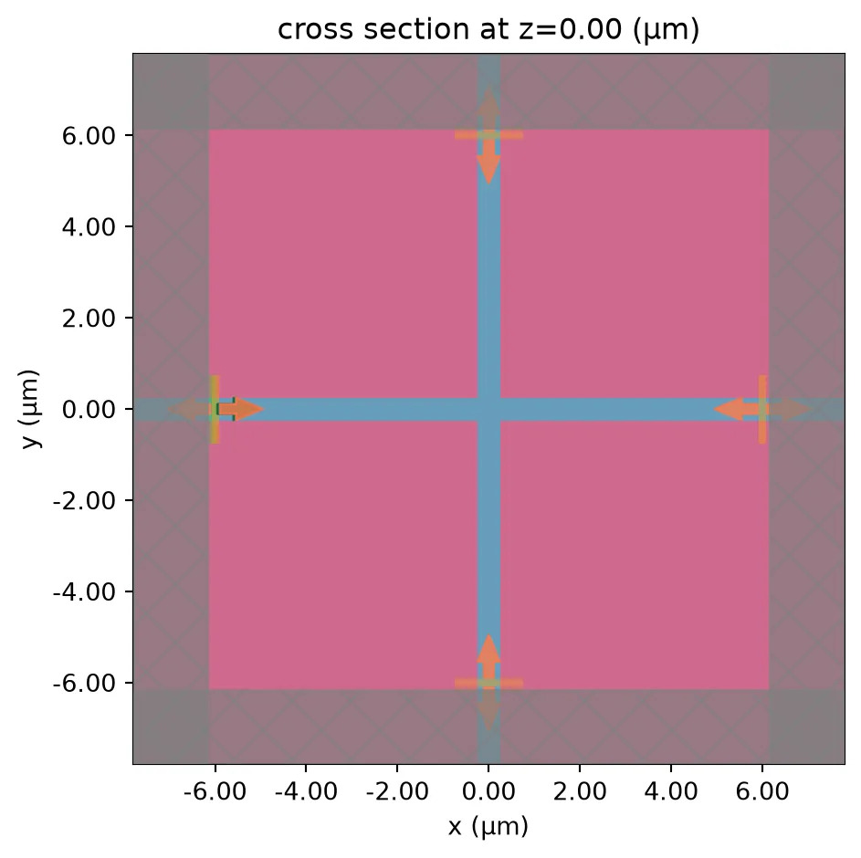
You can extrude any 2D shape into 3D and send it to Tidy3D for simulation and visualization.
import tidy3d as tdextruded = pf.Extruded( td.Medium(permittivity=1.5), cross_poly, (-0.5, 0.5))extruded.to_tidy3d().plot(z=0)