Designing a Power Divider for Wireless Communications 3: Full Structure
The power divider is a key component in modern wireless communications systems. It is usually subject to key performance metrics such as low insertion loss, minimal crosstalk between output ports, and a small footprint. In addition, low pass or bandpass filters are typically incorporated in order to suppress unwanted harmonics and noise in wireless signals. These filters should have a sharp response, quantified by the roll-off rate (ROR), and a wide stopband.
In this 3-part notebook series, we will simulate various stages of the design process of a Wilkinson power divider (WPD) created by Moloudian et al in [1].
- In part one, we started with a simple low pass filter design and improved its filter response in order to achieve a higher roll-off rate (ROR).
- In part two, we added a harmonic suppression circuit to the low pass filter to improve its stopband performance.
- In part three (this notebook), we will implement the full WPD design and compare its performance to a conventional WPD.
import matplotlib.pyplot as pltimport numpy as npimport flex_rf.tidy3d as rfimport flex_rf.web as webrf.config.logging.level = 'ERROR'General Parameters and Mediums
Section titled “General Parameters and Mediums”The simulation bandwidth is chosen to be 0.1-16 GHz. We also include the target operating frequency at 1.8 GHz.
(f_min, f_max) = (0.1e9, 16e9)f_target = 1.8e9bandwidth = rf.FreqRange.from_freq_interval(f_min, f_max)f0 = bandwidth.freq0freqs = np.unique(np.append(f_target, bandwidth.freqs(num_points=601)))The substrate is FR4 and the metallic traces are copper. We assume both materials have constant non-zero loss across the bandwidth: loss tangent of 0.022 for FR4 and conductivity of 6E7 S/m (i.e. 60 S/um) for copper.
# med_FR4 = rf.Medium(permittivity=4.4)med_FR4 = rf.FastDispersionFitter.constant_loss_tangent_model(4.4, 0.022, (f_min, f_max), tolerance_rms=0.004)med_Cu = rf.LossyMetalMedium(conductivity=60, frequency_range=(f_min, f_max))Best weighted RMS error: 0.00351 ━━━━━━━━━━━━━━━━━━━━━━━━━━━━━━━━━━ 100% 0:00:00
Building the Simulation
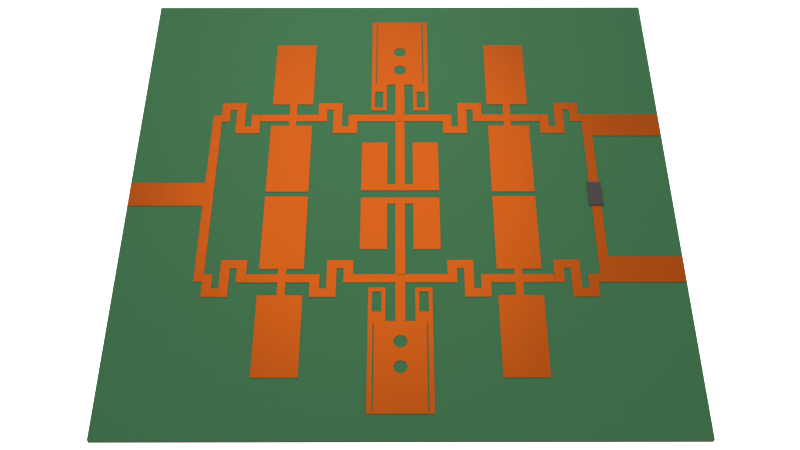
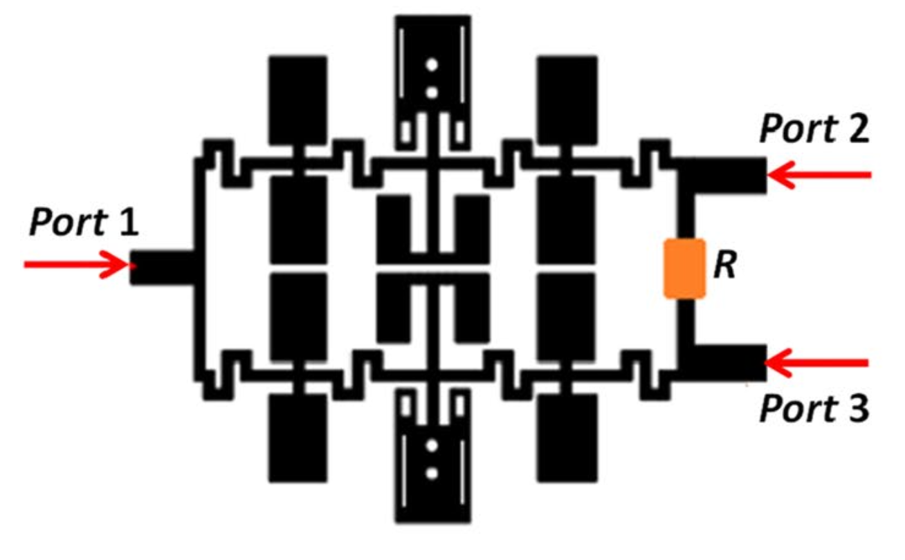
Section titled “Building the Simulation”The full WPD shape is shown in Figure 7(a) of the reference paper and reproduced below. Both arms of the WPD use the low-pass filter with harmonic suppression presented in the second notebook in this series. Please refer to the previous notebooks for more detail on the individual structures.
Structure
Section titled “Structure”All dimensions are taken from [1] where available. Some measurements for the overall WPD are not mentioned, and are instead estimated visually.
# Geometry dimensionsmm = 1000  # Conversion mm to micronH = 0.8 * mm  # Substrate thicknessT = 0.035 * mm  # Metal thickness
# Resonator dimensionsMA, MB, MC, MD = (3.9 * mm, 7.1 * mm, 3.1 * mm, 2.3 * mm)ME, MF, MG, MH = (0.6 * mm, 0.2 * mm, 1.2 * mm, 0.5 * mm)MJ, MK, MM, MN = (4.8 * mm, 0.3 * mm, 0.1 * mm, 0.7 * mm)MP, MQ, MR, MS = (0.1 * mm, 0.7 * mm, 0.4 * mm, 0.3 * mm)
# Suppression structure dimensionsSA, SB, SC, SD = (3 * mm, 11.3 * mm, 4.4 * mm, 6.5 * mm)SE, SF, SG, SH = (2.7 * mm, 1 * mm, 1.7 * mm, 3.7 * mm)SK, SL, SM, SN = (0.5 * mm, 1 * mm, 0.5 * mm, 4.6 * mm)SP, SQ, SR, SS, ST = (0.8 * mm, 1.5 * mm, 2 * mm, 5.9 * mm, 4.6 * mm)
# WPD dimensionsWA, WB = (1.5 * mm, 0.6 * mm)WC = SK / 2 + SN + SK + WB / 2 - WA / 2(WD, WE, WF, WG) = (0.35 * mm, 3 * mm, 0.8 * mm, 0.3 * mm)
# Lumped resistor dimensionsLRL, LRW = (WF, WA)
The low-pass resonator geometry is constructed below.
# Resonator geometrygeom_patch = rf.Box.from_bounds(rmin=(-MA / 2, MH / 2 + MK, 0), rmax=(MA / 2, MH / 2 + MK + MB, T))geom_hole1 = rf.Box.from_bounds( rmin=(-MH / 2 - MN - MF - ME, MH / 2 + MK + MS, 0), rmax=(-MH / 2 - MN - MF, MH / 2 + MK + MS + MG, T),)geom_hole2 = geom_hole1.translated(2 * (MF + MN) + MH + ME, 0, 0)geom_hole3 = rf.Cylinder(center=(0, MH / 2 + MD + MQ, T / 2), radius=MR, length=T, axis=2)geom_hole4 = geom_hole3.translated(0, MQ + 2 * MR, 0)geom_hole5 = rf.Box.from_bounds( rmin=(-MA / 2 + 1.5 * MF, MH / 2 + MK + MS + MG + MQ, 0), rmax=(-MA / 2 + 1.5 * MF + MM, MH / 2 + MK + MB - MP, T),)geom_hole6 = geom_hole5.translated(-2 * geom_hole5.center[0], 0, 0)geom_hole7 = rf.Box.from_bounds( rmin=(-MH / 2 - MN, MH / 2 + MK, 0), rmax=(MH / 2 + MN, MH / 2 + MD, T))geom_line1 = rf.Box.from_bounds(rmin=(-MH / 2, MH / 2, 0), rmax=(MH / 2, MH / 2 + MD, T))for hole in [geom_hole1, geom_hole2, geom_hole3, geom_hole4, geom_hole5, geom_hole6, geom_hole7]: geom_patch -= holegeom_resonator_modified = rf.GeometryGroup(geometries=[geom_line1, geom_patch])Next, the harmonic suppression geometry is constructed.
# Side patchesdef create_side_patch(x0, y0):    """create side patch geometry with feed input centered at (x0, y0)"""    patch_vertices = [x0, y0] + np.array(        [            [SK / 2, 0],            [SK / 2, SP],            [SA / 2, SP],            [SA / 2, SP + ST],            [-SA / 2, SP + ST],            [-SA / 2, SP],            [-SK / 2, SP],            [-SK / 2, 0],        ]    )    patch_geom = rf.PolySlab(vertices=patch_vertices, axis=2, slab_bounds=(0, T))    return patch_geom
geom_patch1 = create_side_patch(-(SB + SA) / 2, SK / 2)geom_patch2 = geom_patch1.reflected((0, -1, 0)).translated(0, 0.3 * mm, 0)geom_patch3 = geom_patch1.reflected((1, 0, 0))geom_patch4 = geom_patch3.reflected((0, -1, 0)).translated(0, 0.3 * mm, 0)# Bend feedlinehalf_bfl_vertices = np.array( [ [-SD / 2, SK / 2], [-SD / 2, -SR / 2 + SK / 2], [-SD / 2 - SM, -SR / 2 + SK / 2], [-SD / 2 - SM, (SR + SK) / 2], [-SD / 2 - SM - SQ, (SR + SK) / 2], [-SD / 2 - SM - SQ, SK / 2], [-SB / 2 - SC, SK / 2], [-SB / 2 - SC, -SK / 2], [-SD / 2 - SM - SQ + SK, -SK / 2], [-SD / 2 - SM - SQ + SK, SR / 2 - SK / 2], [-SD / 2 - SM - SK, SR / 2 - SK / 2], [-SD / 2 - SM - SK, -(SR + SK) / 2], [-SD / 2 + SK, -(SR + SK) / 2], [-SD / 2 + SK, -SK / 2], ])bfl_vertices = np.append(half_bfl_vertices, np.flip(half_bfl_vertices * [-1, 1], axis=0), axis=0)geom_bend_feedline = rf.PolySlab(vertices=bfl_vertices, axis=2, slab_bounds=(0, T))# Bottom middle resonatorbmres_vertices = np.array( [ [-SK / 2, -SK / 2], [-SK / 2, -SK / 2 - SN], [-SK / 2 - SF, -SK / 2 - SN], [-SK / 2 - SF, -SK / 2 - SN - SK + SH], [-SS / 2, -SK / 2 - SN - SK + SH], [-SS / 2, -SK / 2 - SN - SK], [SS / 2, -SK / 2 - SN - SK], [SS / 2, -SK / 2 - SN - SK + SH], [SK / 2 + SF, -SK / 2 - SN - SK + SH], [SK / 2 + SF, -SK / 2 - SN], [SK / 2, -SK / 2 - SN], [SK / 2, -SK / 2], ])geom_bottom_resonator = rf.PolySlab(vertices=bmres_vertices, axis=2, slab_bounds=(0, T))
# Group all harmonic suppression geometry objectsgeom_harmonic_suppression = rf.GeometryGroup( geometries=[ geom_patch1, geom_patch2, geom_patch3, geom_patch4, geom_bend_feedline, geom_bottom_resonator, ])Then, we create the feed lines for the WPD branches.
# WPD feedlines (top half only)half_wpd_in_vertices = [-SB / 2 - SC, WA / 2 + WC] + np.array(    [        [0, -SK / 2],        [0, -SR / 2 + SK / 2],        [-SM, -SR / 2 + SK / 2],        [-SM, (SR + SK) / 2],        [-SM - SQ, (SR + SK) / 2],        [-SM - SQ, SK / 2],        [-SM - SQ - WD, SK / 2],        [-SM - SQ - WD, -WC],        [-SM - SQ - WD - WE, -WC],        [-SM - SQ - WD - WE, -WC - WA / 2],        [-SM - SQ - WD + SK, -WC - WA / 2],        [-SM - SQ - WD + SK, -SK / 2],        [-SM - SQ + SK, -SK / 2],        [-SM - SQ + SK, SR / 2 - SK / 2],        [-SM - SK, SR / 2 - SK / 2],        [-SM - SK, -(SR + SK) / 2],        [SK, -(SR + SK) / 2],        [SK, -SK / 2],    ])half_wpd_out_vertices = [SB / 2 + SC + SK, WA / 2 + WC] + np.array(    [        [0, SK / 2],        [0, -SR / 2 + SK / 2],        [SM, -SR / 2 + SK / 2],        [SM, -SK / 2],        [SM, (SR + SK) / 2],        [SM + SQ, (SR + SK) / 2],        [SM + SQ, SK / 2],        [SM + SQ + WE + WF + WG, SK / 2],        [SM + SQ + WE + WF + WG, SK / 2 - WA],        [SM + SQ + WF + WG, SK / 2 - WA],        [SM + SQ + WF + WG, -WC - WA / 2 + LRW / 2],        [SM + SQ + WG, -WC - WA / 2 + LRW / 2],        [SM + SQ + WG, -SK / 2],        [SM + SQ - SK, -SK / 2],        [SM + SQ - SK, SR / 2 - SK / 2],        [SM + SK, SR / 2 - SK / 2],        [SM + SK, -(SR + SK) / 2],        [-SK, -(SR + SK) / 2],        [-SK, SK / 2],    ])
geom_wpd_feed_in = rf.PolySlab(vertices=half_wpd_in_vertices, axis=2, slab_bounds=(0, T))geom_wpd_feed_out = rf.PolySlab(vertices=half_wpd_out_vertices, axis=2, slab_bounds=(0, T))
Finally, all WPD geometries are consolidated into a single geometry group.
# Create WPD branchesgeom_top_branch = rf.GeometryGroup( geometries=[ geom_wpd_feed_in, geom_wpd_feed_out, geom_harmonic_suppression.translated(0, WC + WA / 2, 0), geom_resonator_modified.translated(0, WC + WA / 2, 0), ])geom_wpd = rf.GeometryGroup(geometries=[geom_top_branch, geom_top_branch.reflected((0, -1, 0))])The associated simulation structures are defined below.
# StructuresLsub, Wsub, _ = geom_wpd.bounding_box.sizeWsub = Wsub * 1.1x0, y0, _ = geom_wpd.bounding_box.centerstr_sub = rf.Structure(    geometry=rf.Box(center=(x0, y0, -H / 2), size=(Lsub, Wsub, H)), medium=med_FR4)str_gnd = rf.Structure(    geometry=rf.Box(center=(x0, y0, -H - T / 2), size=(Lsub, Wsub, T)), medium=med_Cu)str_wpd = rf.Structure(geometry=geom_wpd, medium=med_Cu)
str_list_wpd = [str_sub, str_gnd, str_wpd]  # Full structure list
Monitors
Section titled “Monitors”We define an in-plane field monitor for visualization purposes.
# Field Monitorsmon_1 = rf.FieldMonitor( center=(0, 0, 0), size=(rf.inf, rf.inf, 0), freqs=[f_min, f_target, f0, f_max], name="field in-plane",)mon_list = [mon_1] # List of monitorsLumped Ports and Elements
Section titled “Lumped Ports and Elements”All three ports of the divider are terminated with ohms.
# Lumped portlp_options = {"size": (0, WA, H), "voltage_axis": 2, "impedance": 50}LP1 = rf.LumpedPort(center=(x0 - Lsub / 2, 0, -H / 2), name="LP1", **lp_options)LP2 = rf.LumpedPort(center=(x0 + Lsub / 2, WC + SK / 2, -H / 2), name="LP2", **lp_options)LP3 = rf.LumpedPort(center=(x0 + Lsub / 2, -WC - SK / 2, -H / 2), name="LP3", **lp_options)port_list = [LP1, LP2, LP3] # List of portsThe WPD also has a lumped resistor bridging the two output ports with Ohms.
# Lumped resistorLR1 = rf.LinearLumpedElement( center=(x0 + Lsub / 2 - WE - WF / 2, 0, T), size=(LRL, LRW, 0), name="Resistor", voltage_axis=1, network=rf.RLCNetwork( resistance=100.0, ),)Grid and Boundary
Section titled “Grid and Boundary”By default, the simulation boundary is open (PML) on all sides. We add wavelength/4 padding on all sides to ensure the boundaries do not encroach on the near-field.
# Add paddingpadding = rf.C_0 / f0 / 4sim_LX = Lsub + 2*paddingsim_LY = Wsub + 2*paddingsim_LZ = H + 2*paddingWe use LayerRefinementSpec to automatically refine the grid along corners and edges of the metallic WPD traces. The rest of the grid is automatically created with the minimum grid size determined by the wavelength.
# Layer refinement on resonatorlr_spec = rf.LayerRefinementSpec.from_structures(    structures=[str_wpd],    min_steps_along_axis=1,    corner_refinement=rf.GridRefinement(dl=0.05*mm, num_cells=2),)
# Define overall grid specgrid_spec = rf.GridSpec.auto(    wavelength=rf.C_0 / f0,    min_steps_per_wvl=15,    layer_refinement_specs=[lr_spec],)
Simulation and TerminalComponentModeler
Section titled “Simulation and TerminalComponentModeler”We define the Simulation and TerminalComponentModeler objects below. The latter facilitates a batch port sweep in order to compute the full S-parameter matrix.
As noted in the previous notebook, the device is highly resonant at certain frequencies. To accurately capture its behavior down to the -70 dB level, we should increase the run_time and lower the shutoff level. Conversely, if we were only interested down to -40 dB, it would be OK to cut off the simulation at a much earlier point to save on computational cost.
# Define simulation objectsim = rf.Simulation( center=(x0, y0, 0), size=(sim_LX, sim_LY, sim_LZ), structures=str_list_wpd, lumped_elements=[LR1], grid_spec=grid_spec, monitors=mon_list, run_time=30e-9, shutoff=1e-6, plot_length_units="mm",)# Define TerminalComponentModelertcm = rf.TerminalComponentModeler( simulation=sim, ports=port_list, freqs=freqs, remove_dc_component=False,)Visualization
Section titled “Visualization”Before running the simulation, we check the layout and simulation grid below.
# In-planefig, ax = plt.subplots(figsize=(8, 8))tcm.plot_sim(z=0, ax=ax, monitor_alpha=0)tcm.simulation.plot_grid(z=0, ax=ax, hlim=(-20 * mm, 20 * mm), vlim=(-15 * mm, 15 * mm))plt.show()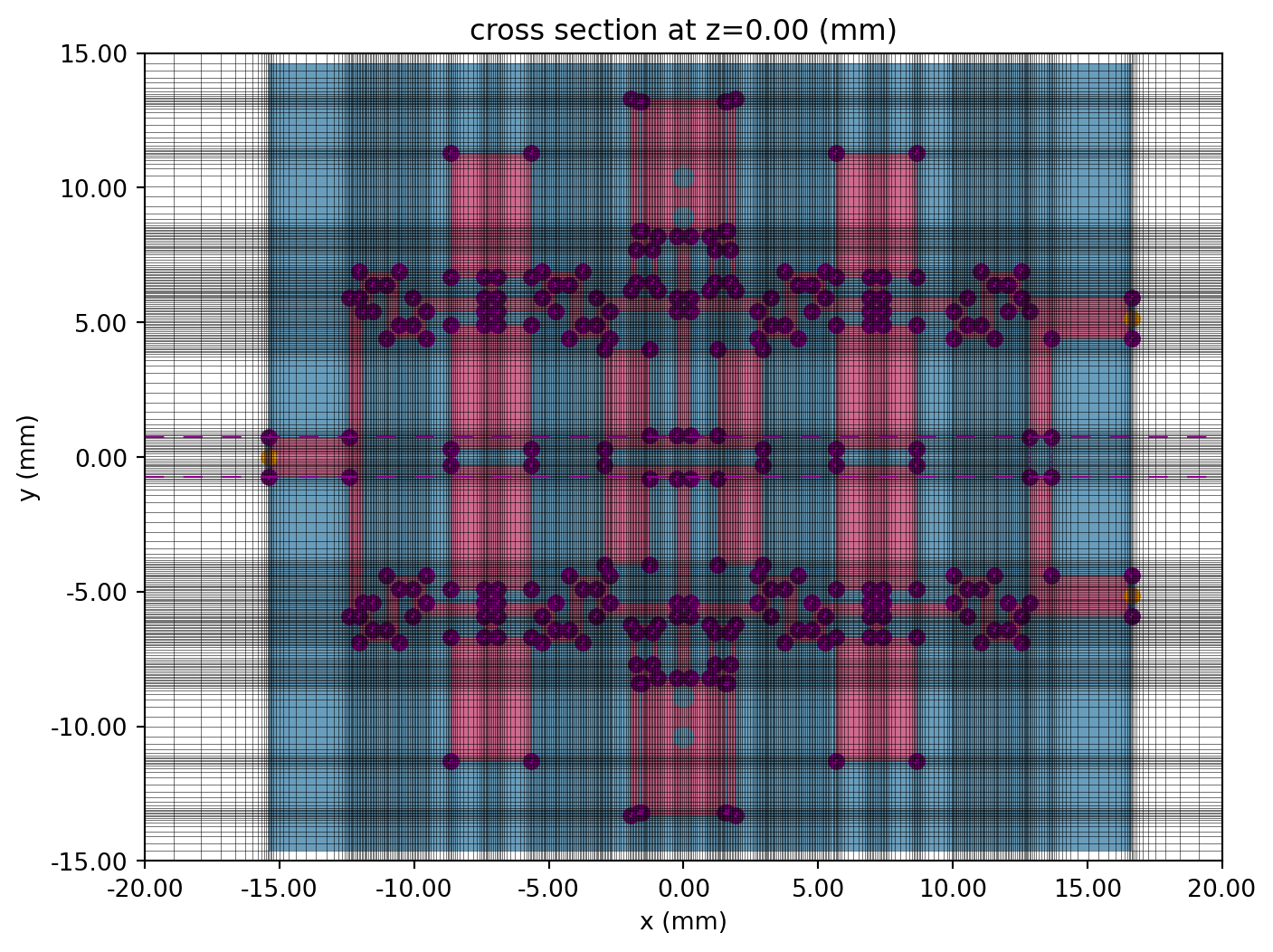
# Cross sectionfig, ax = plt.subplots(2, 1, figsize=(10, 6), tight_layout=True)tcm.plot_sim(x=x0 + Lsub / 2, ax=ax[0], monitor_alpha=0)tcm.simulation.plot_grid( x=x0 - Lsub / 2, ax=ax[0], hlim=(-7 * mm, 7 * mm), vlim=(-1 * mm, 0.1 * mm))tcm.plot_sim(y=0, ax=ax[1], monitor_alpha=0)tcm.simulation.plot_grid(y=0, ax=ax[1], hlim=(-20 * mm, 20 * mm), vlim=(-1 * mm, 0.1 * mm))ax[1].set_aspect(10)plt.show()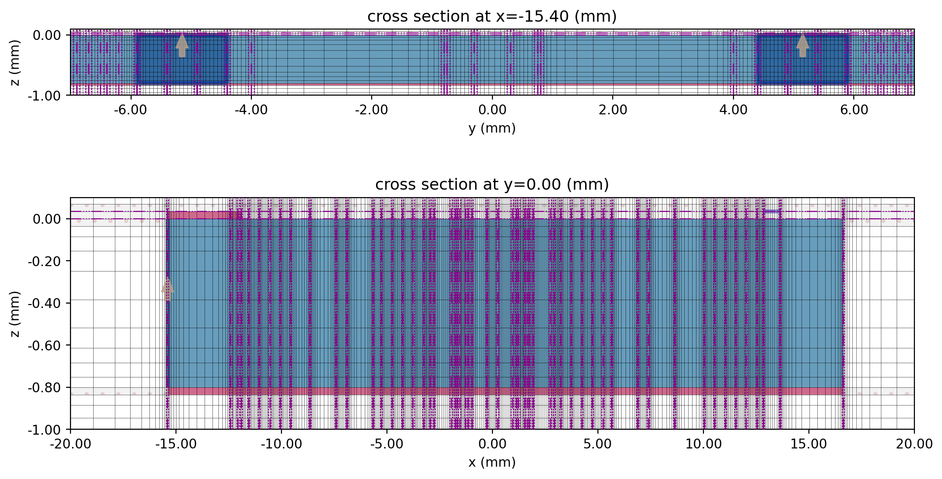
Running the Simulation
Section titled “Running the Simulation”tcm_data = web.run(tcm, task_name="WPD full structure", path="data/tcm_data_full_structure.hdf5", verbose=False)Results
Section titled “Results”Field Profile
Section titled “Field Profile”The simulation monitor data is stored as dict values in the data attribute of the TerminalComponentModelerData instance. Use the port name as the key to access the data associated with the respective port excitation.
sim_data = tcm_data.data["LP1"]The field magnitude profiles at f=f_target and f=f0 (within the stopband) are shown below.
# Field plotsfig, ax = plt.subplots(1, 2, figsize=(10, 4), tight_layout=True)sim_data.plot_field("field in-plane", "E", val="abs", f=f_target, ax=ax[0])ax[0].set_title(f"Field magnitude at f={f_target / 1e9:.1f} GHz")sim_data.plot_field("field in-plane", "E", val="abs", f=f0, ax=ax[1])ax[1].set_title(f"Field magnitude at f={f0 / 1e9:.1f} GHz")for axis in ax: axis.set_xlim(-18 * mm, 18 * mm) axis.set_ylim(-15 * mm, 15 * mm)plt.show()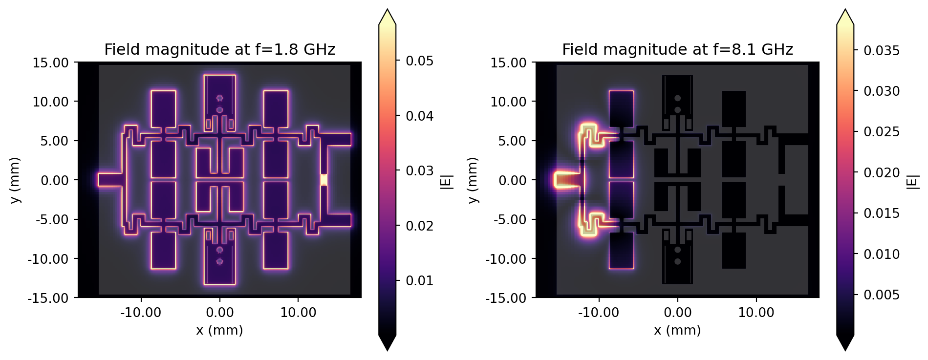
Conventional WPD Model using scikit-rf
Section titled “Conventional WPD Model using scikit-rf”As a basis for comparison, we implement a conventional WPD using the scikit-rf third-party package.
# Import necessary packagesimport skrffrom skrf.media import MLineThe conventional WPD consists of two output ports, each connected to the input port with a quarter-wavelength line of impedance . We construct this circuit below.
# Frequencies and transmission line parametersfreqs_skrf = skrf.Frequency(f_min / 1e9, f_max / 1e9, 601, unit="GHz")mline = MLine(freqs_skrf, w=0.5e-3, h=0.8e-3, t=35e-6, ep_r=4.4, rho=1.67e-08)# WPD resistorR1 = mline.resistor(R=100, name="R1")# WPD quarter wavelength branchesline1 = mline.line(23.7, unit="mm", z0=50 * np.sqrt(2), name="branch1")line2 = mline.line(23.7, unit="mm", z0=50 * np.sqrt(2), name="branch2")# Ports and groundport1 = skrf.Circuit.Port(frequency=freqs_skrf, name="P1", z0=50)port2 = skrf.Circuit.Port(frequency=freqs_skrf, name="P2", z0=50)port3 = skrf.Circuit.Port(frequency=freqs_skrf, name="P3", z0=50)ground = skrf.Circuit.Ground(frequency=freqs_skrf, name="GND", z0=50)# Circuit connectionsconnections = [ [(port1, 0), (line1, 0), (line2, 0)], [(line1, 1), (R1, 0), (port2, 0)], [(line2, 1), (R1, 1), (port3, 0)],]circuit = skrf.Circuit(connections)# Network and S-parametersWPD_skrf = circuit.networkS11dB_skrf = WPD_skrf.s_db[:, 0, 0]S21dB_skrf = WPD_skrf.s_db[:, 1, 0]S32dB_skrf = WPD_skrf.s_db[:, 2, 1]The calculated S-parameters for the conventional WPD will be compared with that of the modified WPD in the next section.
S-parameters
Section titled “S-parameters”The S-parameters of the simulated device can be accessed using the port_in and port_out coordinates from the full smat matrix. Note the use of np.conjugate() to convert from the default physics phase convention to the engineering convention.
smat = tcm_data.smatrix()S11 = np.conjugate(smat.data.isel(port_in=0, port_out=0))S21 = np.conjugate(smat.data.isel(port_in=0, port_out=1))S32 = np.conjugate(smat.data.isel(port_in=1, port_out=2))Below, we compare the performance of the WPD with its conventional counterpart. The return loss shows greatly improved stopband performance over 2.3 to 14 GHz.
fig, ax = plt.subplots(figsize=(10, 4), tight_layout=True)ax.plot(freqs / 1e9, 20 * np.log10(np.abs(S11)), "r", label="|S11|")ax.plot(freqs_skrf.f / 1e9, S11dB_skrf, "r--", label="|S11| (conventional WPD)")ax.add_patch( plt.Rectangle((2.3, 0), 14 - 2.3, -60, fc="gray", alpha=0.2, label="Improved stopband"))ax.legend()ax.set_xlabel("f (GHz)")ax.set_ylabel("dB")ax.set_title("Return loss")ax.grid()plt.show()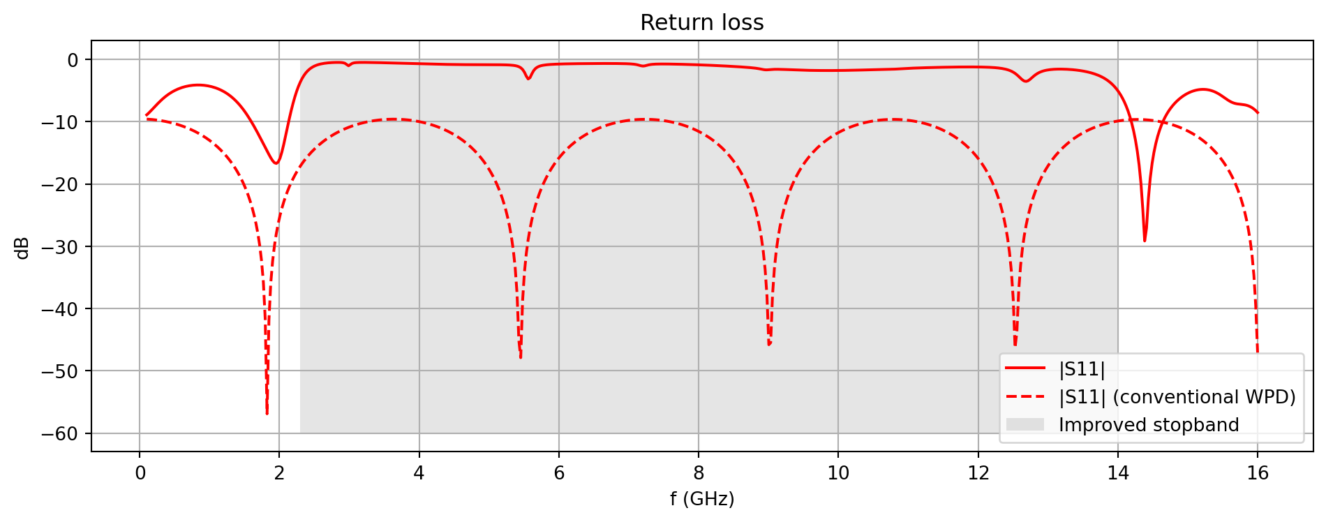
The insertion loss is compared below. At the operating frequency of 1.8 GHz, the proposed WPD has IL = -3.9 dB compared to the ideal -3 dB.
fig, ax = plt.subplots(figsize=(8, 5), tight_layout=True)ax.plot(freqs / 1e9, 20 * np.log10(np.abs(S21)), "b", label="|S21|")ax.plot(freqs_skrf.f / 1e9, S21dB_skrf, "b--", label="|S21| (conventional WPD)")ax.axline(xy1=(0.1, -3), xy2=(f_max / 1e9, -3), color="#555555", ls=":", label="-3 dB @ 1.8 GHz")ax.axline(xy1=(1.8, 0), xy2=(1.8, -10), color="#555555", ls=":")ax.legend()ax.set_xlabel("f (GHz)")ax.set_ylabel("dB")ax.set_title("Insertion loss")ax.set_xlim(0, 3)ax.set_ylim(-10, 0)ax.grid()plt.show()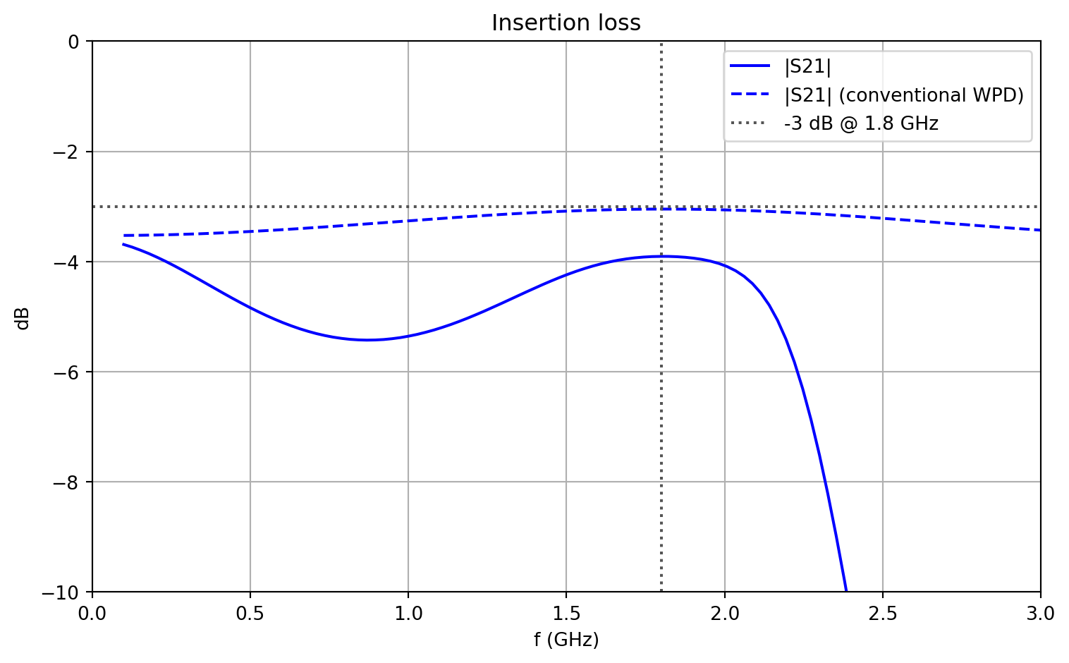
Like the conventional counterpart, the proposed WPD maintains very good isolation (better than -20 dB) between the output ports.
fig, ax = plt.subplots(figsize=(8, 5), tight_layout=True)ax.plot(freqs / 1e9, 20 * np.log10(np.abs(S32)), "g", label="S32")ax.plot(freqs_skrf.f / 1e9, S32dB_skrf, "g--", label="S32 (conventional WPD)")ax.axline(xy1=(1.8, 0), xy2=(1.8, -50), color="#555555", ls=":", label="f = 1.8 GHz")ax.legend()ax.set_xlabel("f (GHz)")ax.set_ylabel("dB")ax.set_title("Output isolation")ax.set_xlim(0, 3)ax.set_ylim(-50, 0)ax.grid()plt.show()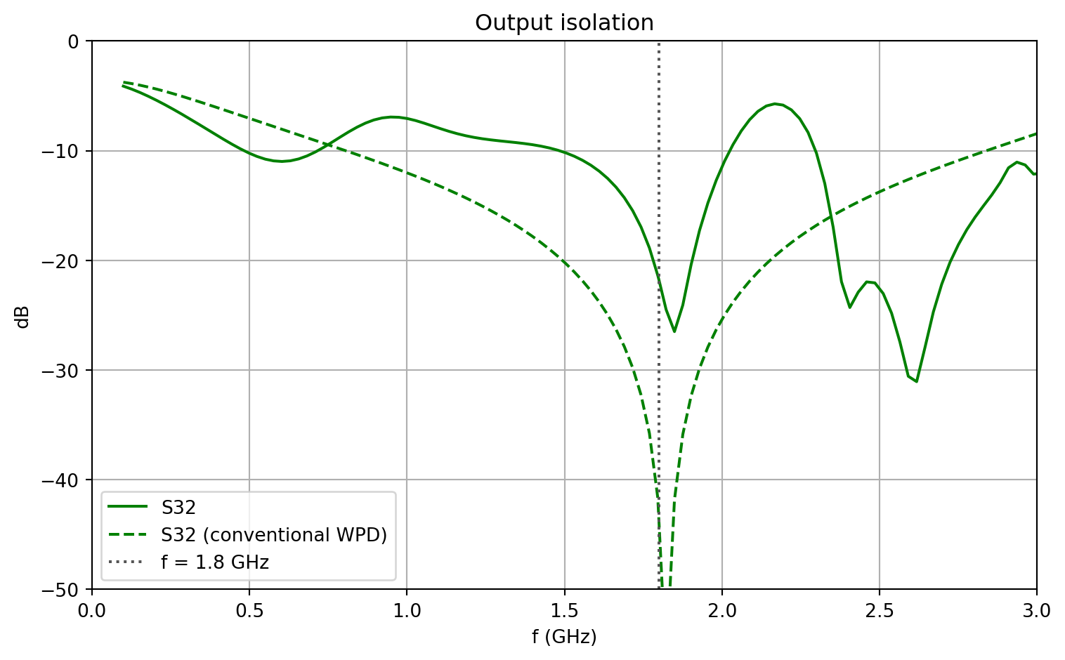
We note that the WPD performance metrics presented in the reference paper are generally better than this simulated device. This is likely due to differences in geometry caused by omitted dimensions in the paper. The authors also note their use of parametric optimization in order to obtain the most ideal dimensional parameters.
Conclusion
Section titled “Conclusion”In this notebook, we simulated the full WPD design presented by Moloudian et al. in [1] and compared its performance to a conventional WPD. The improved WPD features much better signal rejection in the stopband while providing comparable performance at the operating frequency. As noted by the authors, harmonic suppression is a particularly useful feature in modern circuits featuring non-linear elements such as detectors, amplifiers, mixers, and phase shifters.
Reference
Section titled “Reference”[1] Moloudian, G., Soltani, S., Bahrami, S. et al. Design and fabrication of a Wilkinson power divider with harmonic suppression for LTE and GSM applications. Sci Rep 13, 4246 (2023). https://doi.org/10.1038/s41598-023-31019-7