Edge-mounted SMA to Co-planar Waveguide Transition
The subminiature version A (SMA) coaxial connector is an essential component in printed circuit board (PCB) applications. It is commonly used as the interface between the on-board circuit and external components such as antennas or measurement devices.
In this notebook, we model two edge-mounted SMA connectors attached to a grounded co-planar waveguide (CPW). The connector-to-connector insertion and return losses are calculated to ensure proper impedance matching and minimal reflection.
import matplotlib.pyplot as pltimport numpy as npimport flex_rf.tidy3d as rfimport flex_rf.web as webrf.config.logging.level = 'ERROR'Building the Simulation
Section titled “Building the Simulation”Key Parameters
Section titled “Key Parameters”# Frequencies and bandwidth(f_min, f_max) = (1e9, 10e9)f0 = (f_min + f_max) / 2freqs = np.linspace(f_min, f_max, 301)Important geometry dimensions are defined below. The default length unit is microns, so we introduce a mm conversion factor.
mm = 1000  # Conversion factor mm to microns
# Coaxial dimensions (50 ohm)R0 = 0.635 * mm  # Coax inner radiusR1 = 2.125 * mm  # Coax outer radius
# Substrate overall dimensionsH = 1.57 * mm  # Substrate thicknessLsub, Wsub = (83 * mm, 30 * mm)  # PCB board dimensions
# Transmission line dimensionsT = 0.038 * mm  #  Metal thicknessWS = 2.58 * mm  # Signal trace widthG = 1 * mm  # CPW gap widthWG = 5 * mm  # Side ground trace width
# Via dimensionsVR = 0.5 * mm  # Via radiusVP = 3 * mm  # Via pitch, longitudinalVL = 3 * mm  # Via pitch, transverseVS = 1 * mm  # Via start z-coordinate
# Edge mount dimensionsVoffset = 0.125 * mm  # SMA connector vertical offset
Medium and Structures
Section titled “Medium and Structures”Below, we define the materials used in the model:
- PTFE for the SMA dielectric core
- Gold for the SMA body
- FR4 for the PCB substrate
- Copper for the PCB traces
med_FR4 = rf.Medium(permittivity=4.4)med_PTFE = rf.Medium(permittivity=2.1)med_Cu = rf.LossyMetalMedium(conductivity=60, frequency_range=(f_min, f_max)) # [S/um]med_Au = rf.LossyMetalMedium(conductivity=41, frequency_range=(f_min, f_max)) # [S/um]The SMA geometry is imported from a STL file, and then translated and rotated to the appropriate position. The SMA core is created from a rf.Cylinder instance. To ensure a close fit, we initialize the SMA core to be slightly larger than the inner radius and use Boolean subtraction to cut it to size.
# Import SMA geometrygeom_SMA = rf.TriangleMesh.from_stl(filename="./misc/SMA_model.stl", scale=mm, origin=(0, 0, 0))geom_SMA = (geom_SMA.rotated(np.pi / 2, 0)).rotated(np.pi, 2)geom_SMA = geom_SMA.translated(0, Voffset, 0)
# Create SMA dielectric coregeom_SMA_diel = rf.Cylinder(    center=(0, Voffset, -6 * mm / 2), radius=1.1 * R1, length=6 * mm, axis=2)geom_SMA_diel -= geom_SMA
We also make a copy for a second connector.
# Make copy for second connectorgeom_SMA2 = (geom_SMA.rotated(np.pi, 1)).translated(0, 0, Lsub)geom_SMA_diel2 = (geom_SMA_diel.rotated(np.pi, 1)).translated(0, 0, Lsub)The substrate and CPW geometries are created below.
# Substrategeom_sub = rf.Box.from_bounds(rmin=(-Wsub / 2, -H - T, 0), rmax=(Wsub / 2, -T, Lsub))
# Transmission line and connecting structuresgeom_sig = rf.Box.from_bounds(rmin=(-WS / 2, -T, 0), rmax=(WS / 2, 0, Lsub))geom_gnd1 = rf.Box.from_bounds(rmin=(-WS / 2 - G - WG, -T, 0), rmax=(-WS / 2 - G, 0, Lsub))geom_gnd2 = geom_gnd1.reflected((1, 0, 0))geom_line = rf.GeometryGroup(geometries=[geom_sig, geom_gnd1, geom_gnd2])geom_gnd = rf.Box.from_bounds(rmin=(-Wsub / 2, -H - 2 * T, 0), rmax=(Wsub / 2, -H - T, Lsub))
To ensure proper transmission in the high frequency range, we create a via fence that encloses the signal trace.
# Create via fencedef create_via_hole(xpos, zpos):    geom = rf.Cylinder(center=(xpos, -H / 2 - T, zpos), axis=1, length=H, radius=VR)    return geom
geom_via_array = []zpos = VSwhile zpos < Lsub - VS + 0.1 * mm:    for xpos in [-VL, VL]:        geom_via_array += [create_via_hole(xpos, zpos)]    zpos += VP
geom_via_group = rf.GeometryGroup(geometries=geom_via_array)
We combine the previously defined geometries and materials into Structure instances, ready for simulation.
# Create structuresstr_SMA = rf.Structure(geometry=geom_SMA, medium=med_Au)str_SMA2 = rf.Structure(geometry=geom_SMA2, medium=med_Au)str_SMA_diel = rf.Structure(geometry=geom_SMA_diel, medium=med_PTFE)str_SMA_diel2 = rf.Structure(geometry=geom_SMA_diel2, medium=med_PTFE)str_sub = rf.Structure(geometry=geom_sub, medium=med_FR4)str_line = rf.Structure(geometry=geom_line, medium=med_Cu)str_gnd = rf.Structure(geometry=geom_gnd, medium=med_Cu)str_vias = rf.Structure(geometry=geom_via_group, medium=med_Cu)
# List of all structuresstructure_list = [    str_SMA,    str_SMA2,    str_SMA_diel,    str_SMA_diel2,    str_sub,    str_line,    str_gnd,    str_vias,]
Grid and Boundaries
Section titled “Grid and Boundaries”The simulation boundaries are open (PML) on all sides. We introduce a padding of wavelength/2 on all sides to ensure that the external boundaries do not encroach on the near-field.
# Define simulation size and centerpadding = rf.C_0 / f0 / 2sim_LZ = Lsub + paddingsim_LX = Wsub + paddingsim_LY = 5 * mm + paddingsim_center = (0, 0, Lsub / 2)The grid refinement strategy is as follows:
- Use
LayerRefinementSpecfor PCB metallic layers - Use
MeshOverrideStructurefor SMA dielectric core and metal via fences
# Define layer refinement speclr_options = {    "corner_refinement": rf.GridRefinement(dl=0.1 * mm, num_cells=2),    "min_steps_along_axis": 1,}lr1 = rf.LayerRefinementSpec.from_structures(structures=[str_line], **lr_options)lr2 = rf.LayerRefinementSpec.from_structures(structures=[str_gnd], **lr_options)
# Define mesh override around SMA core and viasrbox1 = rf.MeshOverrideStructure(    geometry=geom_SMA_diel.bounding_box, dl=(0.2 * mm, 0.2 * mm, 0.2 * mm))rbox2 = rf.MeshOverrideStructure(    geometry=geom_SMA_diel2.bounding_box, dl=(0.2 * mm, 0.2 * mm, 0.2 * mm))rbox_vias = []for geom in geom_via_array:    rbox_vias += [        rf.MeshOverrideStructure(geometry=geom.bounding_box, dl=(0.3 * mm, None, 0.3 * mm))    ]
The overall grid specification is defined below.
# Define overall grid specificationgrid_spec = rf.GridSpec.auto( min_steps_per_wvl=15, wavelength=rf.C_0 / f_max, layer_refinement_specs=[lr1, lr2], override_structures=[rbox1, rbox2] + rbox_vias,)Monitors
Section titled “Monitors”We define some field monitors for visualization purposes below.
# Field Monitormon_1 = rf.FieldMonitor(    center=(0, -T - H / 2, 0),    size=(rf.inf, 0, rf.inf),    freqs=[f_min, f0, f_max],    name="field in-plane",)mon_2 = rf.FieldMonitor(    center=(0, 0, 0),    size=(0, rf.inf, rf.inf),    freqs=[f_min, f0, f_max],    name="field cross section",)
# List of all monitorsmonitor_list = [mon_1, mon_2]Wave ports are positioned along the coaxial section of each SMA connector.
# Wave port position and dimensionwp_offset = 4 * mm  # longitudinal offsetw_port = 4.6 * mm  # port width and height
# Define wave portsWP1 = rf.WavePort(    center=(0, Voffset, -wp_offset),    size=(w_port, w_port, 0),    mode_spec=rf.MicrowaveModeSpec(target_neff=np.sqrt(2.1)),    direction="+",    name="WP1",    frame=None,)WP2 = WP1.updated_copy(    center=(0, Voffset, Lsub + wp_offset),    direction="-",    name="WP2",)
Defining Simulation and TerminalComponentModeler
Section titled “Defining Simulation and TerminalComponentModeler”The Simulation and TerminalComponentModeler instances are defined below.
sim = rf.Simulation(    center=sim_center,    size=(sim_LX, sim_LY, sim_LZ),    grid_spec=grid_spec,    structures=structure_list,    monitors=monitor_list,    run_time=5e-9,    plot_length_units="mm",    symmetry=(1, 0, 0),)
tcm = rf.TerminalComponentModeler(    simulation=sim,    ports=[WP1, WP2],    freqs=freqs,)
Visualization
Section titled “Visualization”Before running, it is a good idea to check the structure layout and simulation grid. Below, the top and side cross-sections of the structure are shown, along with the wave port sources (green arrow) and internal modal absorbers (blue arrow).
fig, ax = plt.subplots(1, 2, figsize=(10, 10), tight_layout=True)tcm.plot_sim( y=-T, ax=ax[0], monitor_alpha=0, hlim=(-20 * mm, 20 * mm), vlim=(-15 * mm, Lsub + 15 * mm))tcm.plot_sim( x=0, ax=ax[1], monitor_alpha=0, hlim=(-10 * mm, 10 * mm), vlim=(-15 * mm, Lsub + 15 * mm))plt.show()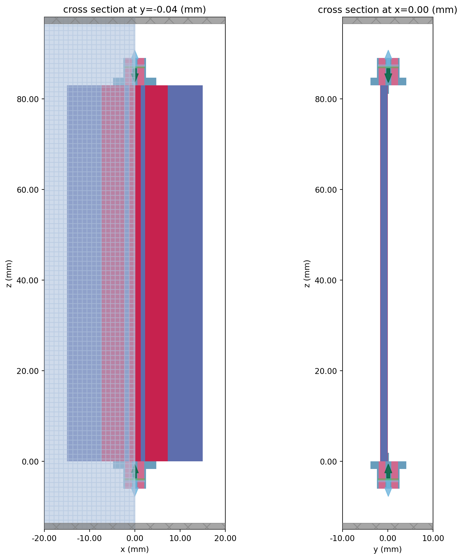
The grid in the SMA-CPW transition region is shown below. The mesh override regions are boxed with dotted black lines.
fig, ax = plt.subplots(figsize=(10, 10), tight_layout=True)tcm.simulation.plot_grid(y=-T - H / 2, ax=ax)tcm.plot_sim( y=-T - H / 2, ax=ax, monitor_alpha=0, hlim=(-20 * mm, 20 * mm), vlim=(-10 * mm, 10 * mm))plt.show()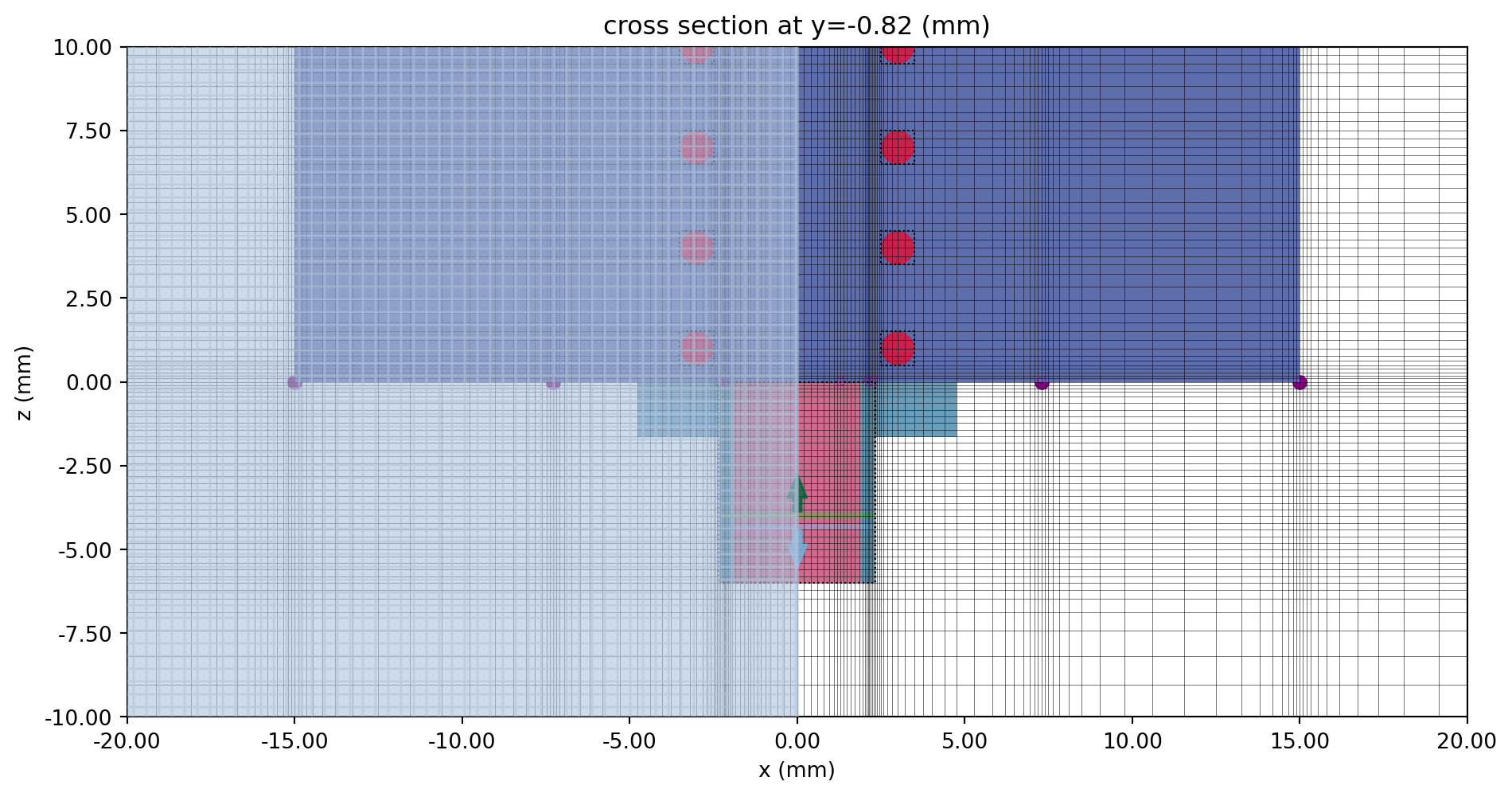
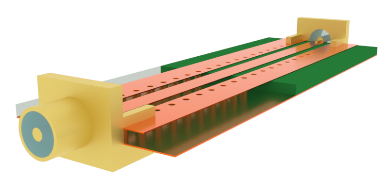
We can also visualize the setup in 3D.
sim.plot_3d()Running the Simulation
Section titled “Running the Simulation”The simulation is executed below.
tcm_data = web.run(tcm, task_name="sma_connector", path="data/sma_connector.hdf5", verbose=False)Results
Section titled “Results”Field Profile
Section titled “Field Profile”The field monitor data is accessed from the .data attribute of the TerminalComponentModelerData result. The key is in the format <wave port name>@<mode number>, for example WP1@0. (In this case, there is only one mode.)
# Extract simulation datasim_data = tcm_data.data["WP1@0"]Below, the Ex and Ey field components are plotted along the top and side cross-sections respectively.
fig, ax = plt.subplots(1, 2, figsize=(10, 8), tight_layout=True)f_plot = f_maxsim_data.plot_field("field in-plane", field_name="Ex", val="real", f=f_plot, ax=ax[0])sim_data.plot_field("field cross section", "Ey", val="real", f=f_plot, ax=ax[1])for axis in ax: axis.set_ylim(-15 * mm, Lsub + 10 * mm) axis.set_xlim(-20 * mm, 20 * mm)plt.show()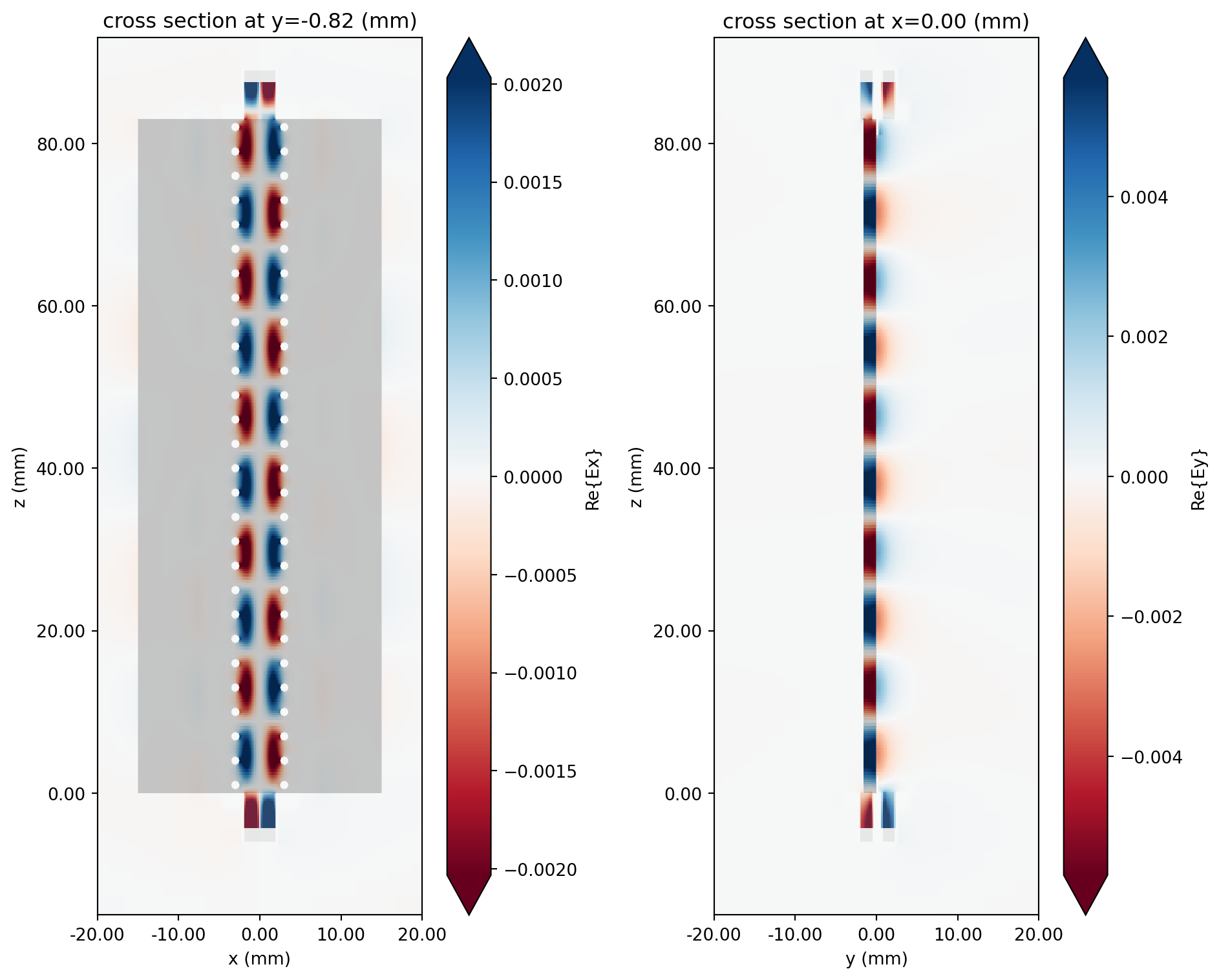
S-parameters
Section titled “S-parameters”The S-matrix data is extracted using the smatrix() method. To access a specific S_ij parameter, use the corresponding port_in and port_out attributes. Note the use of np.conjugate to convert the S-parameter from the physics phase convention (current Flex RF default) to the usual electrical engineering convention.
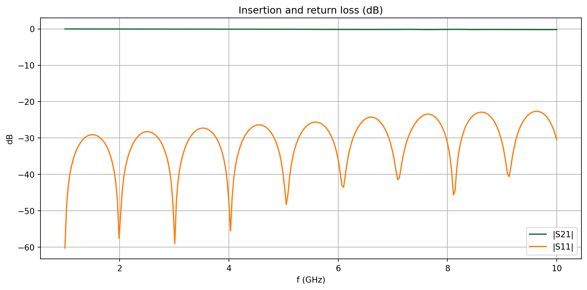
# Extract S-matrix and S-parameterssmat = tcm_data.smatrix()S11 = np.conjugate(smat.data.isel(port_in=0, port_out=0))S21 = np.conjugate(smat.data.isel(port_in=0, port_out=1))The insertion and return losses are plotted below. We observe excellent transmission and minimal reflection across the frequency band, indicating that the impedance of the SMA connector is well-matched to that of the on-board transmission line.
fig, ax = plt.subplots(figsize=(10, 5), tight_layout=True)ax.plot(freqs / 1e9, 20 * np.log10(np.abs(S21)), label="|S21|")ax.plot(freqs / 1e9, 20 * np.log10(np.abs(S11)), label="|S11|")ax.set_title("Insertion and return loss (dB)")ax.set_xlabel("f (GHz)")ax.set_ylabel("dB")ax.legend()ax.grid()plt.show()