RF Electrode in a Microring Modulator
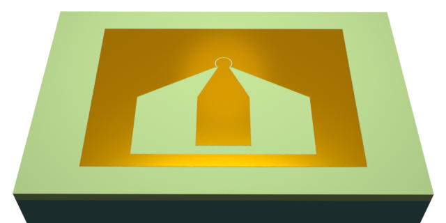
The microring resonator (MRR) is a key component in modern photonics design. In this notebook, we model the RF electrode in a silicon-on-insulator MRR, which carries the electrical signal responsible for optical modulation.
In a full fidelity model, the MRR would require multiphysics coupling of thermal, charge, optical, and RF simulations. For this RF-only demonstration, we will approximate the reverse bias p-n junction, responsible for the optical phase modulation, with a lumped RC element. The focus will be on minimizing return loss within the operational bandwidth.
import gdstkimport matplotlib.pyplot as pltimport numpy as npimport flex_rf.tidy3d as rfimport flex_rf.web as webrf.config.logging.level = 'ERROR'Building the Model
Section titled “Building the Model”Key Parameters and Materials
Section titled “Key Parameters and Materials”The bandwidth of the simulation is 10-100 GHz.
# Frequency bandwidthf_min, f_max = (10e9, 100e9)f0 = (f_max + f_min) / 2freqs = np.linspace(f_min, f_max, 101)
# Dimensionslen_inf = 1e5bounds_electrode = (2.62, 3.02)bounds_oxide = (-3.017, 2.62)bounds_sub = (-len_inf, -3.017)TM = bounds_electrode[1] - bounds_electrode[0]  # electrode thickness
The equivalent RC parameters of the reverse bias p-n junction can be estimated using a lumped circuit model. Details of the calculation are presented in section 2.2.3 of Ref [1].
# Lumped electrical parametersC_lumped = 17.325e-15 # FaradsR_lumped = 113.12 # OhmsZref = 50 # Ohms, port reference impedanceThe relevant materials are defined below.
# Mediumsmed_sub = rf.Medium(permittivity=12.3) # Si substratemed_oxide = rf.Medium(permittivity=4.2) # SiO2med_metal = rf.LossyMetalMedium(conductivity=17, frequency_range=(f_min, f_max)) # Metal [S/um]Geometry
Section titled “Geometry”In lieu of building the electrode geometry from scratch, we will import a pre-constructed 2D shape from GDS. It is then extruded to the appropriate thickness.
# Load GDS and build metal electrode geometrygds_mrr = gdstk.read_gds("misc/mrr-electrode.gds")g_electrode = rf.Geometry.from_gds(    gds_mrr["MRR"], gds_layer=12, gds_dtype=0, slab_bounds=bounds_electrode, axis=2)
# Dielectric layersg_oxide = rf.Box.from_bounds(    rmin=(-len_inf, -len_inf, bounds_oxide[0]), rmax=(len_inf, len_inf, bounds_oxide[1]))g_sub = rf.Box.from_bounds(    rmin=(-len_inf, -len_inf, bounds_sub[0]), rmax=(len_inf, len_inf, bounds_sub[1]))
The geometries are combined with the corresponding mediums into Structure instances below.
# Structuresstr_sub = rf.Structure(geometry=g_sub, medium=med_sub)str_oxide = rf.Structure(geometry=g_oxide, medium=med_oxide)str_electrode = rf.Structure(geometry=g_electrode, medium=med_metal)structure_list = [str_sub, str_oxide, str_electrode]Grid and Boundary
Section titled “Grid and Boundary”The external boundaries of the simulation are terminated with Perfectly Matched Layers (PMLs) by default. We add some space padding around the electrode, although we do not expect it to radiate significantly.
# Simulation center and sizesim_X0, sim_Y0, sim_Z0 = (30, -30, 0)sim_LX, sim_LY, sim_LZ = (450, 300, 400)The grid should be able to resolve key features in the electrode, such as the gap and corners, for accurate results. To this end, we use the LayerRefinementSpec feature to automatically analyze the electrode geometry and generate an appropriately fine mesh. For added fidelity, we also define a MeshOverrideStructure around the microring region that constrains maximum grid size in the in-plane directions.
# Layer refinementlr1 = rf.LayerRefinementSpec.from_structures(    structures=[str_electrode],    corner_refinement=rf.GridRefinement(dl=1, num_cells=2),    min_steps_along_axis=1,)
# Mesh overriderefine_box = rf.MeshOverrideStructure(    geometry=rf.Box.from_bounds(        rmin=(16.5, 1, bounds_electrode[0]), rmax=(43.5, 27, bounds_electrode[1])    ),    dl=(1, 1, None),)
The overall grid specification is defined below. The rest of the simulation grid is automatically generated based on the shortest wavelength.
# Grid specificationgrid_spec = rf.GridSpec.auto( min_steps_per_wvl=15, wavelength=rf.C_0 / f_max, layer_refinement_specs=[lr1], override_structures=[refine_box],)Monitors
Section titled “Monitors”We define a field monitor just below the electrode plane for visualization purposes.
# Field Monitormon_1 = rf.FieldMonitor(    center=(sim_X0, sim_Y0, bounds_electrode[0]),    size=(len_inf, len_inf, 0),    freqs=[f_min, f0, f_max],    name="field in-plane",)
monitor_list = [mon_1]
Lumped Ports and Elements
Section titled “Lumped Ports and Elements”We will use lumped ports and elements in this model since the structure is extremely sub-wavelength.
# Lumped portLP1 = rf.LumpedPort( center=(30, -85, bounds_electrode[1]), size=(60, 10, 0), voltage_axis=1, name="LP1", impedance=Zref,)The equivalent RC circuit representing the p-n junction is defined below.
# Define equivalent RC series circuitresistor = rf.LumpedCircuitComponent(element_type='R', node_plus='0', node_minus='1', value=R_lumped)cap = rf.LumpedCircuitComponent(element_type='C', node_plus='1', node_minus='2', value=C_lumped)circuit = rf.CircuitImpedanceModel( components=[resistor, cap], port_node_plus='0', port_node_minus='2')# Define lumped element using the RC circuitLE1 = rf.LinearLumpedElement( center=(30, 24.795, bounds_electrode[1]), size=(2, 2.2, 0), voltage_axis=1, network=circuit, name="LumpedRC",)Simulation and TerminalComponentModeler
Section titled “Simulation and TerminalComponentModeler”The simulation and TerminalComponentModeler instances are defined below.
sim = rf.Simulation(    center=(sim_X0, sim_Y0, sim_Z0),    size=(sim_LX, sim_LY, sim_LZ),    grid_spec=grid_spec,    structures=structure_list,    monitors=monitor_list,    lumped_elements=[LE1],    run_time=1e-10,)
tcm = rf.TerminalComponentModeler(    simulation=sim,    ports=[LP1],    freqs=freqs,)
Visualization
Section titled “Visualization”Before running the simulation, let us visualize the geometry and grid. The lumped port (green) and lumped RC element (blue) are also depicted below.
# Metal electrode planefig, ax = plt.subplots(1, 2, figsize=(10, 3), tight_layout=True)tcm.simulation.plot_grid(z=bounds_electrode[1], ax=ax[0])tcm.plot_sim(z=bounds_electrode[1], ax=ax[0], monitor_alpha=0, hlim=(-150, 210), vlim=(-125, 50))tcm.simulation.plot_grid(z=bounds_electrode[0], ax=ax[1])tcm.plot_sim(z=bounds_electrode[1], ax=ax[1], monitor_alpha=0, hlim=(15, 45), vlim=(0, 30))plt.show()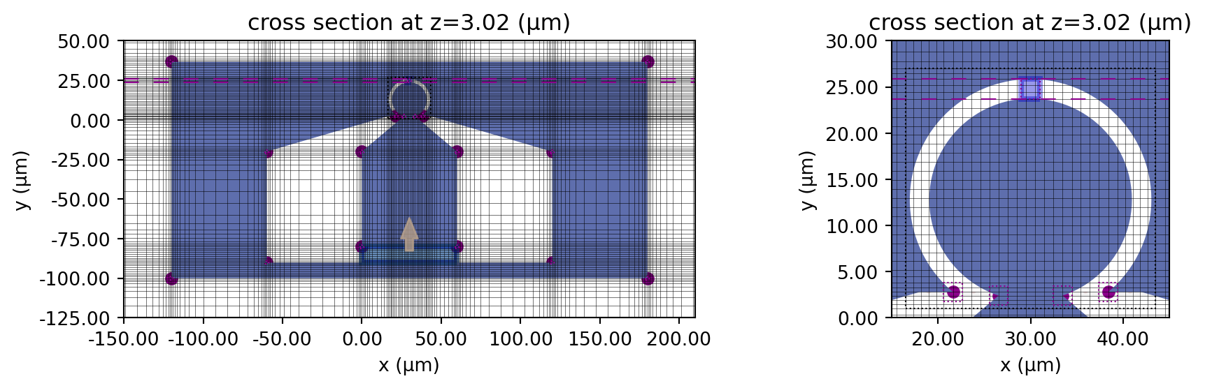
We can also use the 3D viewer.
sim.plot_3d()Running the Simulation
Section titled “Running the Simulation”The simulation is executed below.
tcm_data = web.run(tcm, task_name="microring_electrode", path="data/microring_electrode.hdf5", verbose=False)Results
Section titled “Results”S-parameter
Section titled “S-parameter”We extract and plot S11 below.
# Extract S11smat = tcm_data.smatrix()S11 = np.conjugate(smat.data.squeeze())The return loss (RL) is shown below. From the RL plot, we observe that the electrode has a -3 dB bandwidth of up to 55 GHz.
# Plot return lossfig, ax = plt.subplots(figsize=(10, 4), tight_layout=True)ax.plot(freqs / 1e9, 20 * np.log10(np.abs(S11)))ax.set_title("Return Loss (dB)")ax.set_ylabel("dB")ax.set_xlabel("f (GHz)")ax.grid()plt.show()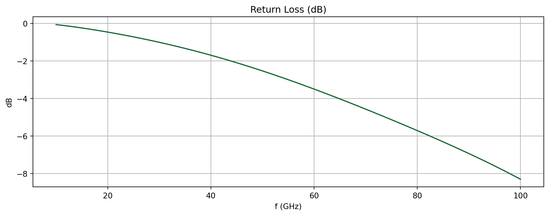
Field profile
Section titled “Field profile”We extract the field monitor data and plot the in-plane field magnitude at the center frequency below.
# Extract monitor datasim_data = tcm_data.data["LP1"]
# Plot field monitor datafig, ax = plt.subplots(figsize=(10, 5), tight_layout=True)f_plot = f0sim_data.plot_field("field in-plane", field_name="E", val="abs", f=f_plot, ax=ax)ax.set_xlim(-150, 210)ax.set_ylim(-150, 80)plt.show()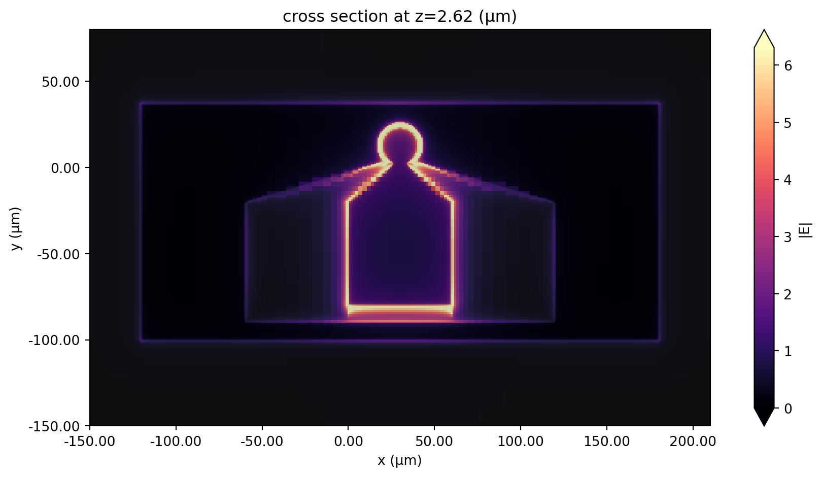
Reference
Section titled “Reference”[1] Wang, Zhao. “Silicon micro-ring resonator modulator for inter/intra-data centre applications.” PhD diss., 2017.