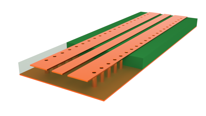
Grounded co-planar waveguide with via fence
Co-planar waveguide (CPWs) transmission lines offer many advantages, including better EM shielding, ease of fabrication, and lower radiation loss when compared to microstrips. However, conventional CPWs can be susceptible to coupling to higher-order modes in nearby structures, thus introducing undesirable resonances that restrict the operating bandwidth of the CPW. In particular, at high frequencies, the side ground planes in a conventional CPW can support higher-order resonances that radiate similarly to a patch antenna.
One solution is to introduce via fences on either side of the signal line. This reduces the transverse electrical size of the CPW and “pushes” the resonances out beyond the design bandwidth of the CPW. It also provides the added benefit of better shielding from EM interference.
In this notebook, we will simulate some of the designs investigated in this paper:
- Sain, Arghya, and Kathleen L. Melde, “Impact of ground via placement in grounded coplanar waveguide interconnects.” IEEE Transactions on Components, Packaging and Manufacturing Technology 6.1 (2015): 136-144.
We begin by simulating a conventional CPW with a bottom ground plane to demonstrate the undesirable resonant effect. Then, we will compare it to a design with via fences. Finally, we will test a setup fabricated by Sain et al. in order to validate the simulation results.
import matplotlib.pyplot as pltimport numpy as npimport flex_rf.tidy3d as rfimport flex_rf.web as web
rf.config.logging.level = "ERROR"
Building the simulation
Section titled “Building the simulation”Key parameters and materials
Section titled “Key parameters and materials”The key parameters for this model are the operating frequency range, the geometry, and the material properties. These are defined below.
# Frequencyf_min, f_max = (1e9, 100e9) # Frequency range (Hz)f0 = (f_max + f_min) / 2 # Center frequencyfreqs = np.linspace(f_min, f_max, 301) # Sample frequency pointsfield_mon_freqs = np.linspace(f_min, f_max, 21) # Frequency points for field monitor data
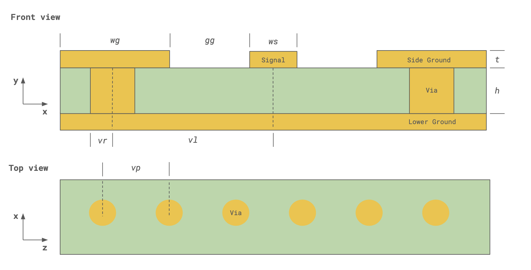
# CPW Geometrylen_inf = 1e5 # Effective infinityws = 177.8 # Signal strip widthwg = 1600 # Ground strip widtht = 17.78 # Conductor thicknessh = 101.6 # Substrate thicknessgg = 101.6 # Gap between signal and side groundL = 6000 # CPW line length
# Via geometryvr = 76.2 # Via radiusvp = 287.3 # Via pitch (longitudinal spacing)vl = 400 # Via transverse spacing (from center of signal strip)es = 127 # Distance from first/last via to CPW start/end
# Overall simulation size and centersim_size = (5600, 1000, 7500)sim_center = (0, 500 - h - t, 0)Both the substrate and metal are assumed to have constant loss over the frequency range. The materials used for the simulation are defined below.
# Material propertiescond = 58 # Metal conductivity in S/umeps = 3.5 # Relative permittivity, substratelosstan = 0.002 # Loss tangent, substratemed_sub = rf.FastDispersionFitter.constant_loss_tangent_model( eps, losstan, (f_min, f_max), tolerance_rms=3e-4)med_metal = rf.LossyMetalMedium(conductivity=cond, frequency_range=(f_min, f_max), name="Metal")med_air = rf.Medium(permittivity=1.0, name="Air")Best weighted RMS error: 0.00029 ━━━━━━━━━━━━━━━━━━━━━━━━━━━━━━━━━━ 100% 0:00:00
Geometry construction
Section titled “Geometry construction”We start by creating all the planar structures (substrate and metal strips). The ground plane and substrate are assumed to be infinite in width and length.
# Substratestr_sub = rf.Structure(    geometry=rf.Box(center=(0, -h / 2, 0), size=(len_inf, h, len_inf)), medium=med_sub)
# Signal stripstr_sig = rf.Structure(geometry=rf.Box(center=(0, t / 2, 0), size=(ws, t, L)), medium=med_metal)
# Side and bottom groundsstr_gnd1 = rf.Structure(    geometry=rf.Box(center=((ws + wg) / 2 + gg, t / 2, 0), size=(wg, t, L)), medium=med_metal)str_gnd2 = rf.Structure(    geometry=rf.Box(center=(-(ws + wg) / 2 - gg, t / 2, 0), size=(wg, t, L)), medium=med_metal)str_gnd3 = rf.Structure(    geometry=rf.Box(center=(0, -h - t / 2, 0), size=(len_inf, t, len_inf)), medium=med_metal)
We define a reusable function to create the via structure at a given (x, z) position.
def create_via(xpos, zpos):    """Create one via structure at given x and z positions"""    via_structure = rf.Structure(        geometry=rf.Cylinder(center=(xpos, -h / 2, zpos), radius=vr, length=h, axis=1),        medium=med_metal,    )
    return via_structure
Then, we loop over all x- and z-positions to create the via fence.
# create viasstr_via_fence = []for zpos in np.arange(-L / 2 + es, L / 2 - es + 10, vp): for xpos in [-vl, vl]: str_via_fence += [create_via(xpos, zpos)]We consolidate the structures into two lists, with and without the via fence. We will use these in two separate simulations later.
# List of all structures (with and without via fence)str_list_1 = [str_sub, str_gnd1, str_gnd2, str_gnd3, str_sig]str_list_2 = [str_sub, str_gnd1, str_gnd2, str_gnd3, str_sig] + str_via_fenceWe use the LayerRefinementSpec feature to automatically apply refinement to metal edges and corners.
def create_layer_refinement_spec(structure_list):    """Creates a LayerRefinementSpec using the bounding box of the given list of structures"""    lr_spec = rf.LayerRefinementSpec.from_structures(        structures=structure_list,        axis=1,        min_steps_along_axis=1,        corner_refinement=rf.GridRefinement(            dl=t, num_cells=2        ),  # snap to corners and apply added refinement    )
    return lr_spec
# Apply layer refinement to top and bottom metal planeslr_spec_1 = create_layer_refinement_spec([str_sig, str_gnd1, str_gnd2])lr_spec_2 = create_layer_refinement_spec([str_gnd3])
For the rest of the model, we define the grid size using the min_steps_per_sim_size parameter since the simulation is largely sub-wavelength.
# Define overall grid specificationgrid_spec = rf.GridSpec.auto( min_steps_per_sim_size=100, wavelength=rf.C_0 / f_max, layer_refinement_specs=[lr_spec_1, lr_spec_2],)Boundaries
Section titled “Boundaries”We use the Perfectly Matched Layer (PML) boundary condition on all sides except the bottom. For the bottom boundary, we use the PEC condition for simplicity, since it is adjacent to the infinite bottom ground plane.
boundary_spec = rf.BoundarySpec( x=rf.Boundary.pml(), y=rf.Boundary(plus=rf.PML(), minus=rf.PECBoundary()), z=rf.Boundary.pml(),)Monitors
Section titled “Monitors”We define two field monitors for visualization purposes. One is in the longitudinal substrate plane, while the other is along the transverse plane halfway down the CPW.
field_mon_1 = rf.FieldMonitor(    center=(0, -h / 2, 0),    size=(rf.inf, 0, rf.inf),    freqs=field_mon_freqs,    name="field (substrate plane)",)
field_mon_2 = rf.FieldMonitor( center=(0, 0, 0), size=(rf.inf, rf.inf, 0), freqs=field_mon_freqs, name="transverse field")In general, we have a choice of using WavePort or LumpedPort to excite the structure. Because we are probing the resonances of this finite length CPW, it makes more sense to use the LumpedPort.
The lumped port is positioned in the gap between the signal strip and side ground planes, with the port voltage axis aligned along the x-direction. The design impedance of the CPW is around 50 ohms, so each lumped port should be 100 ohms.
LP_len = 50  # Lumped port length
LP1 = rf.LumpedPort(    center=((ws + gg) / 2, t / 2, -L / 2 + LP_len / 2),    size=(gg, 0, LP_len),    name="LP1",    impedance=100,  # in Ohms    voltage_axis=0,  # 0 = x-axis)
LP2 = LP1.updated_copy(name="LP2", center=((ws + gg) / 2, t / 2, L / 2 - LP_len / 2))
Simulation and TerminalComponentModeler
Section titled “Simulation and TerminalComponentModeler”The Simulation object contains all of the previously defined specifications. The first simulation implements the conventional CPW layout without via fences.
sim_without_via_fence = rf.Simulation( size=sim_size, center=sim_center, medium=med_air, # background medium is air/vacuum grid_spec=grid_spec, boundary_spec=boundary_spec, structures=str_list_1, monitors=[field_mon_1, field_mon_2], run_time=3.5e-9, # simulation run time symmetry=(1, 0, 0), # odd symmetry in x-direction plot_length_units="mm", # set plot units to mm)The TerminalComponentModeler is a wrapper class that conducts a port sweep on the simulation. The lumped ports are set here.
tcm_without_via_fence = rf.TerminalComponentModeler( simulation=sim_without_via_fence, # simulation, previously defined ports=[LP1, LP2], # lumped ports, previously defined freqs=freqs, # S-parameter frequency points)Visualization
Section titled “Visualization”Before executing the simulation, we plot the structure and grid along various planes to check that they are adequately set up and resolved.
# Inspect transverse grid near CPW gapfig, ax = plt.subplots(figsize=(10, 5))sim_without_via_fence.plot(z=1, ax=ax)sim_without_via_fence.plot_grid(z=1, ax=ax, hlim=(0, 500), vlim=(-130, 50))plt.show()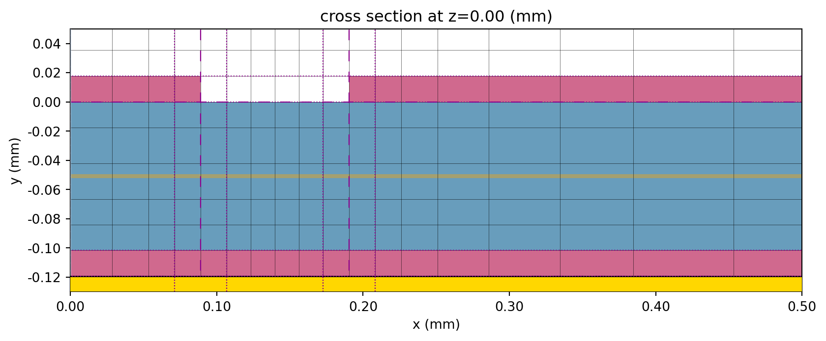
# Inspect longitudinal gridfig, ax = plt.subplots(figsize=(6, 8))sim_without_via_fence.plot(y=1, ax=ax)sim_without_via_fence.plot_grid(y=1, ax=ax, hlim=(0, 3000), vlim=(-L / 2 - 200, L / 2 + 200))ax.set_aspect(0.5)plt.show()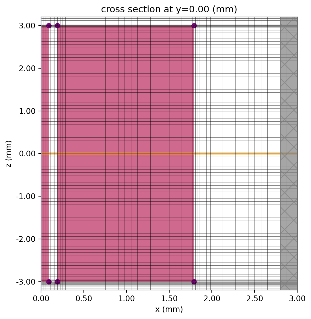
We can also use the built-in 3D viewer.
sim_without_via_fence.plot_3d()The lumped ports can be viewed using the plot_sim() method of the TCM.
# Plot lumped portsfig, ax = plt.subplots(1, 2, figsize=(8, 6), tight_layout=True)tcm_without_via_fence.plot_sim(y=t / 2, ax=ax[0])ax[0].set_xlim(-1000, 1000)ax[0].set_ylim(L / 2 - 1000, L / 2 + 1000)tcm_without_via_fence.plot_sim(y=t / 2, ax=ax[1])ax[1].set_xlim(-1000, 1000)ax[1].set_ylim(-L / 2 - 1000, -L / 2 + 1000)plt.show()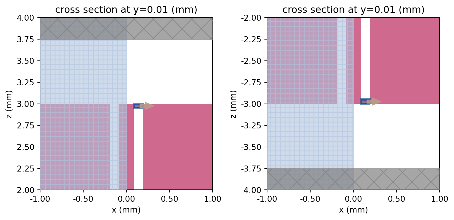
Conventional CPW with Lower Ground Plane
Section titled “Conventional CPW with Lower Ground Plane”We execute the TCM to obtain the S-parameter matrix.
tcm_data_without_via_fence = web.run( tcm_without_via_fence, task_name="GCPW no via fence", path="data/tcm_data_without_via_fence.hdf5", verbose=False,)# Calculate s-matrixs_matrix = tcm_data_without_via_fence.smatrix()The S-parameters are extracted and S21 is plotted below.
S11 = np.conjugate(s_matrix.data.sel(port_in="LP1", port_out="LP1"))S21 = np.conjugate(s_matrix.data.sel(port_in="LP1", port_out="LP2"))S11dB = 20 * np.log10(np.abs(S11))S21dB = 20 * np.log10(np.abs(S21))# Plotting S-parametersfig, ax = plt.subplots(figsize=(10, 3))ax.plot(freqs / 1e9, S21dB)ax.set_xlim(0, 100)ax.set_ylim(-30, 1)ax.set_title("Insertion loss")ax.set_ylabel("|S21| (dB)")ax.set_xlabel("f (GHz)")plt.show()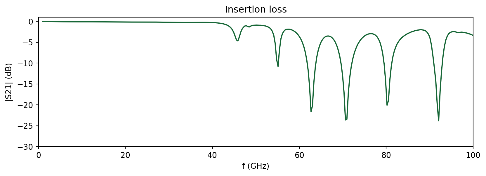
At frequencies above 40 GHz, higher-order resonances in the CPW limit its usable bandwidth. The resonant frequencies are partly determined by the width and length of the side ground planes. We visualize one such resonance near f=71 GHz below.
In order to view the field monitor data, we load it from the dictionary object associated with the TCM data.
# Load monitor datasim_data_without_via_fence = tcm_data_without_via_fence.data["LP1"]# Field plotfig, ax = plt.subplots(figsize=(10, 8))sim_without_via_fence.plot_structures(y=0, ax=ax, fill=False)sim_data_without_via_fence.plot_field( "field (substrate plane)", field_name="E", val="abs", f=71e9, ax=ax, eps_alpha=0.2)ax.set_title("Field magnitude in substrate plane (f=71 GHz)")plt.show()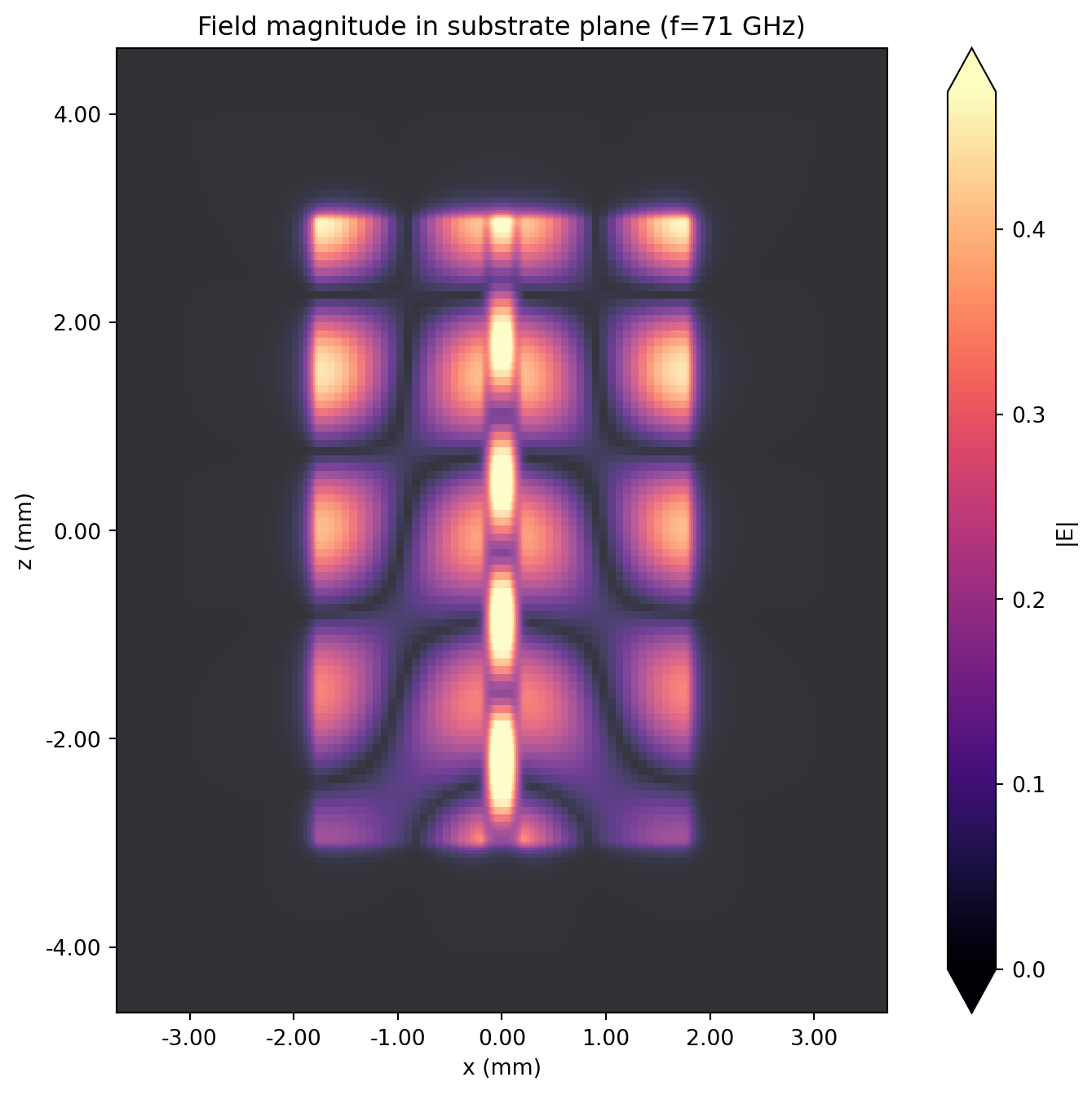
# Field plotfig, ax = plt.subplots(figsize=(12, 3))sim_without_via_fence.plot_structures(z=0, ax=ax, fill=False)sim_data_without_via_fence.plot_field("transverse field", field_name="E", val="abs", f=71e9, ax=ax)ax.set_title("Field magnitude at z=0 (f=71 GHz)")ax.set_ylim(-100, 500)ax.set_xlim(-2000, 2000)plt.show()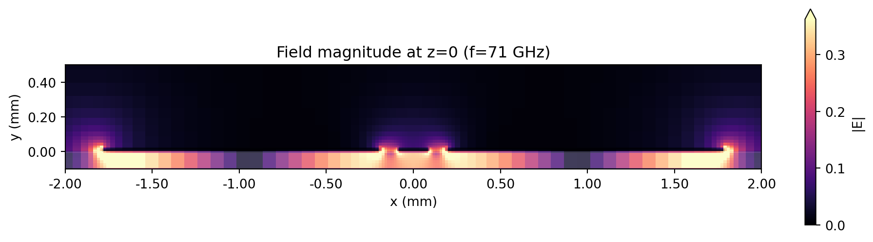
The higher-order mode in the side ground planes is clearly visible from the field plots above.
Adding Via Fences
Section titled “Adding Via Fences”In order to restrict the higher-order modes, we will add via fences on both sides of the signal strip.
We make use of the updated_copy() method to easily modify the structure list, without having to redefine from scratch the Simulation or TerminalComponentModeler objects.
sim_via_fence = sim_without_via_fence.updated_copy(structures=str_list_2)tcm_via_fence = tcm_without_via_fence.updated_copy(simulation=sim_via_fence)Executing the simulation below.
tcm_data_via_fence = web.run( tcm_via_fence, task_name="GCPW via fence", path="data/tcm_data_via_fence.hdf5", verbose=False)# Calculate s-matrixs_matrix_vf = tcm_data_via_fence.smatrix()Like before, we extract and plot the insertion loss.
# Extracting S-parametersS11_vf = np.conjugate(s_matrix_vf.data.sel(port_in="LP1", port_out="LP1"))S21_vf = np.conjugate(s_matrix_vf.data.sel(port_in="LP1", port_out="LP2"))S11dB_vf = 20 * np.log10(np.abs(S11_vf))S21dB_vf = 20 * np.log10(np.abs(S21_vf))# Plotting S-parametersfig, ax = plt.subplots(figsize=(10, 3))ax.plot(freqs / 1e9, S21dB_vf, label="with via fence")ax.plot(freqs / 1e9, S21dB, label="without via fence")ax.set_title("Insertion loss")ax.set_xlabel("f (GHz)")ax.set_ylabel("|S21| (dB)")ax.legend()plt.show()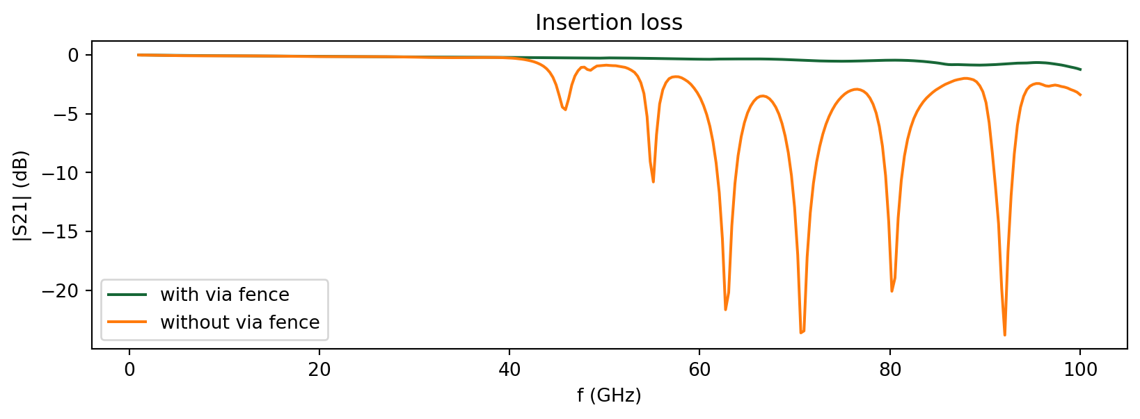
The addition of the via fences has suppressed the higher-order resonances in the side ground planes. This allows the CPW to have a much wider operational bandwidth. Let’s compare the fields at the same resonance point below.
# Load monitor datasim_data_via_fence = tcm_data_via_fence.data["LP1"]# Field plotfig, ax = plt.subplots(1, 2, figsize=(10, 5), tight_layout=True)sim_data_without_via_fence.plot_field( "field (substrate plane)", field_name="E", val="abs", f=71e9, ax=ax[0], eps_alpha=0.2)sim_data_via_fence.plot_field( "field (substrate plane)", field_name="E", val="abs", f=71e9, ax=ax[1], eps_alpha=0.2)plt.show()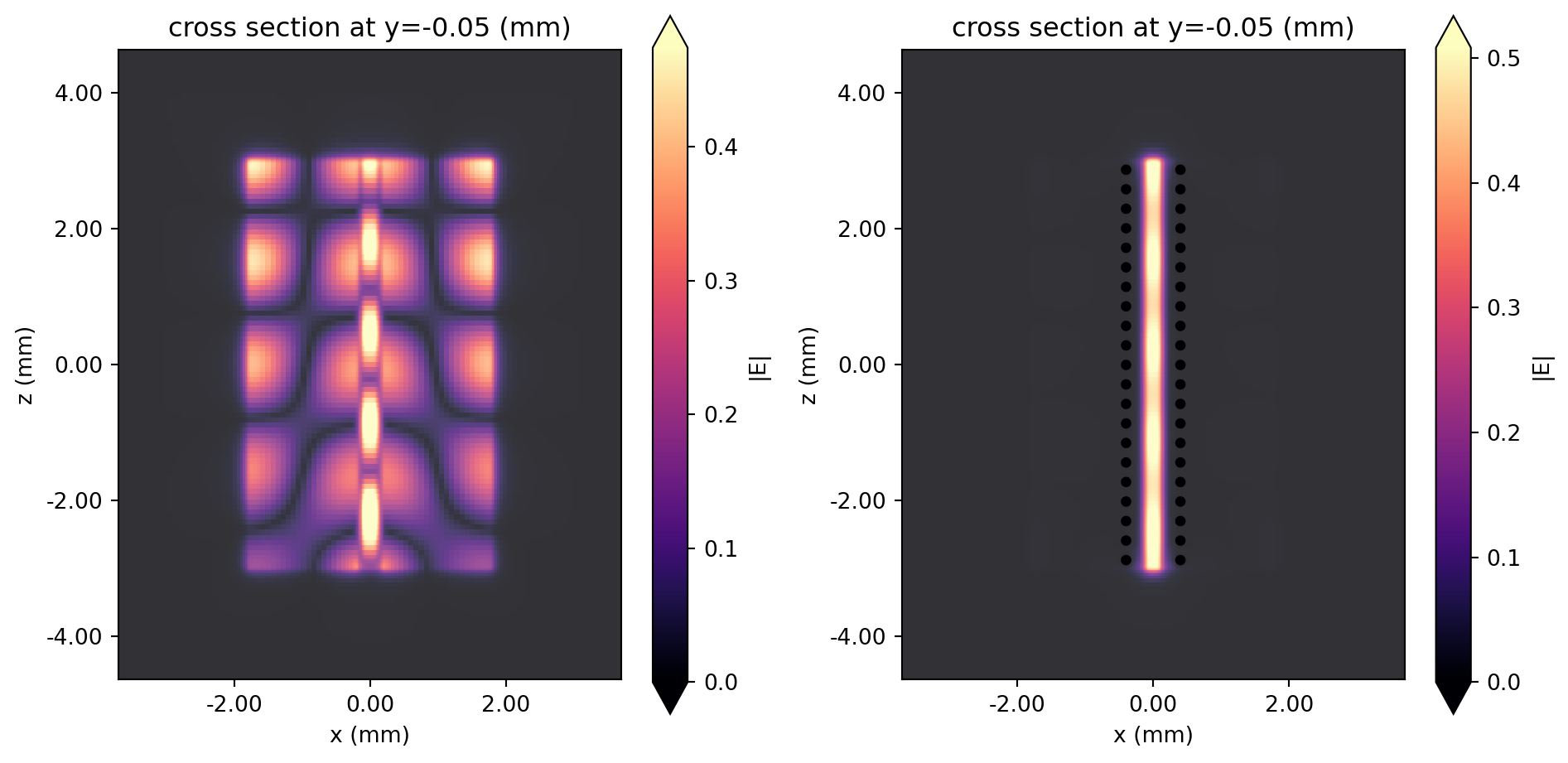
With the via fence, the field is very well confined to the region close to the signal line.
Experimental Validation
Section titled “Experimental Validation”For validation, Sain et al. fabricated a design shown in Fig. 9 in the reference paper. They used HFSS, a commercial FEM tool, to compare with the measured data. In this section, we will do the same with our RF solver.
# Geometry parameters for experimental setupwg2 = 1200vl2 = 1212.7vp2 = 508es2 = 460
# Create new side ground planesstr_gnd4 = rf.Structure(    geometry=rf.Box(center=((ws + wg2) / 2 + gg, t / 2, 0), size=(wg2, t, L)), medium=med_metal)str_gnd5 = rf.Structure(    geometry=rf.Box(center=(-(ws + wg2) / 2 - gg, t / 2, 0), size=(wg2, t, L)), medium=med_metal)
# Create via fencestr_via_fence_2 = []for zpos in np.arange(-L / 2 + es2, L / 2 - es2 + 10, vp2):    for xpos in [-vl2, vl2]:        str_via_fence_2 += [create_via(xpos, zpos)]
# Structure liststr_list_3 = [str_sub, str_gnd4, str_gnd5, str_gnd3, str_sig] + str_via_fence_2# Update simulation and TCMfreqs_exp = np.linspace(1e9, 40e9, 301)sim_exp = sim_without_via_fence.updated_copy( structures=str_list_3, monitors=[],)tcm_exp = tcm_without_via_fence.updated_copy(simulation=sim_exp, freqs=freqs_exp)Let’s example the setup in 3D.
sim_exp.plot_3d()We run the simulation below.
tcm_data_exp = web.run(tcm_exp, task_name="GCPW experiment", path="data/tcm_data_exp.hdf5", verbose=False)# Calculate s-matrixs_matrix_exp = tcm_data_exp.smatrix()# Extract S-parametersS11_exp = np.conjugate(s_matrix_exp.data.sel(port_in="LP1", port_out="LP1"))S21_exp = np.conjugate(s_matrix_exp.data.sel(port_in="LP1", port_out="LP2"))S11dB_exp = 20 * np.log10(np.abs(S11_exp))S21dB_exp = 20 * np.log10(np.abs(S21_exp))# Import reference datafreqs_sain_measured, S21dB_sain_measured = np.loadtxt( "./misc/gcpw_sain_experimental.csv", delimiter=",", unpack=True, skiprows=1)freqs_sain_hfss, S21dB_sain_hfss = np.loadtxt( "./misc/gcpw_sain_simulated.csv", delimiter=",", unpack=True, skiprows=1)# Plot S21fig, ax = plt.subplots(figsize=(10, 3))ax.plot( freqs_exp / 1e9, 20 * np.log10(np.abs(S21_exp)), label="RF photonics solver (Flexcompute)", color="#328362",)ax.plot( freqs_sain_measured, S21dB_sain_measured, "--", color="#888888", label="Measured (Sain et al.)")ax.plot(freqs_sain_hfss, S21dB_sain_hfss, ":", color="#888888", label="HFSS (Sain et al.)")ax.set_title("S21 (dB)")ax.set_xlabel("f (GHz)")ax.legend()plt.show()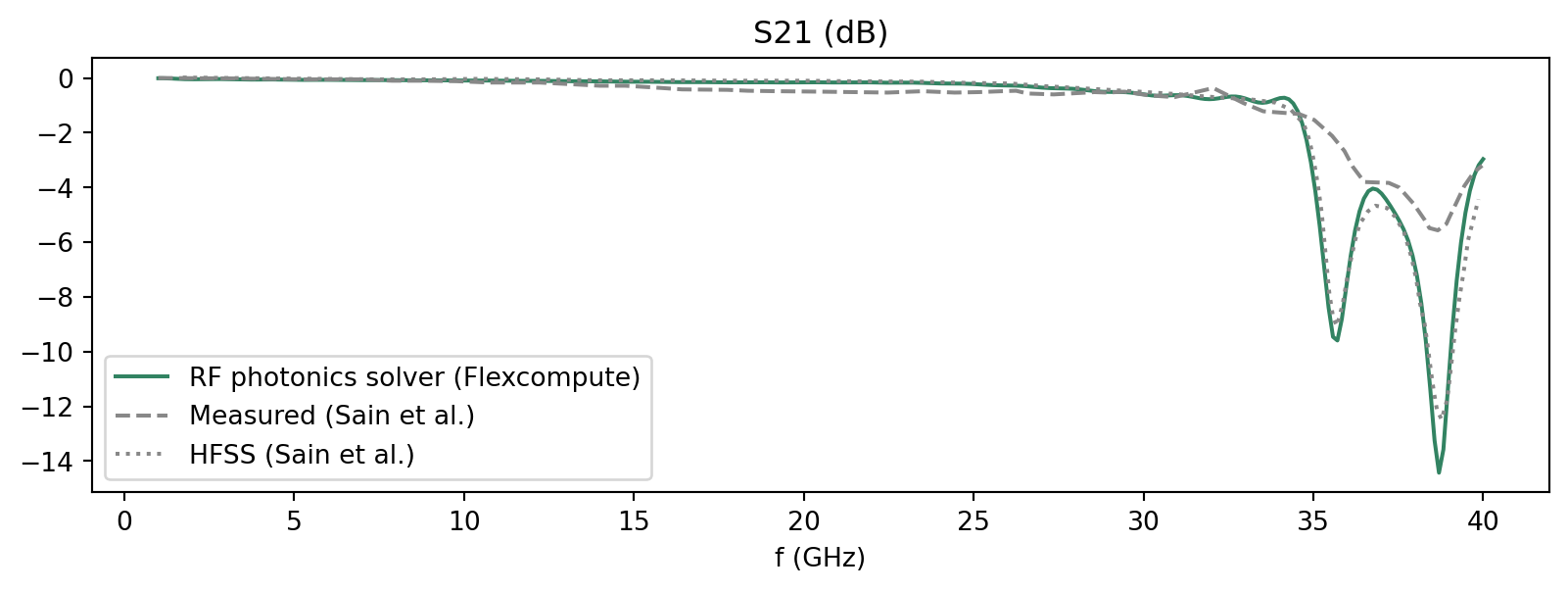
We observe a good match with the data from Sain et al.
Remaining discrepancy with the measured data, as noted by Sain et al., can be attributed to metal surface roughness as well as deviations in the fabrication measurements.
Reference
Section titled “Reference”[1] Sain, Arghya, and Kathleen L. Melde, “Impact of ground via placement in grounded coplanar waveguide interconnects.” IEEE Transactions on Components, Packaging and Manufacturing Technology 6.1 (2015): 136-144.